Background Of The Invention
-
The present application is a continuation-in-part
of co-pending U.S. Patent Application Serial No.
08/682,487 filed July 17, 1996. The entire text of the
above-referenced disclosure is specifically
incorporated by reference herein without disclaimer.
Field of the Invention
-
The invention relates generally to interconnection
systems for use in electrical and electronic
connectors, including two-piece, card edge, and wire
interconnections. In particular, this invention
relates to an improvement in fine pitch connectors for
connecting printed circuit boards (PCB) for
applications including board stacking, vertical to
vertical, mother to daughter, vertical to right angle
and/or straddle, and in one aspect relates to an
improved connector comprising a plug and a socket each
having four rows of electrical contact elements.
Description of the Prior Art
-
The art is replete with connectors for making
multiple interconnections between boards, between
boards and discreet wires, and between boards and
flexible circuits, all of which have the goal of making
the most interconnections per area of board space.
-
For example, board to board connectors are
illustrated in PCT Application WO 93/03513 published 18
February 1993 and in US Patent No. 5,380,225 issued
January 10, 1995. The publication illustrates a board
to board interconnection of the hermaphrodicitic design
wherein the connector portions have the identical shape
and are mated in a single orientation to ensure proper
electrical connection. Further, the solder tails of
the connector portions are spaced 1 mm and each portion
of the connector is formed to have a row of passive
contacts (fixed contact surfaces) and a row of active
contacts (movable spring contract surface). This
relationship, according to the publication, reduces the
required overall PCB to PCB stack height (the distance
between two coupled circuit boards) because only one
spring height is required. Further, since each
connector has both spring contacts and fixed contacts,
the spring force on the movable contacts is the same
from its initial mate height until the final mate
height. The movable spring contacts are deflected by
the same predetermined amount regardless of the PCB to
PCB stack height. The latter patent referenced above
teaches the use of a connector making two rows of
contacts, each row including staggered contacts. This
connector however discloses the contact elements of a
passive nature in the plug 1a and the active, flexible
contacts in the jack 1. The contact elements are
however all spaced and staggered to form the four rows
of contacts of equal number in one connector,
lengthwise thereof. Other PCB to PCB interconnections
are shown in WO 90/16093 where opposed spring contacts
were employed which increased the stack height.
-
USA Patent No. 4,804,336 discloses a D-shaped
connector having improved density by using staggered
rows of pin contacts in the body to double the density
from the normal 50 contacts to 100. As in Patent
5,380,225, staggering and duplicity alone does not
serve to adequately improve the density of the
interconnections to be made and still reduce the stack
height.
-
Historically, separable two-piece connectors are
either of pin and socket style or ribbon style. Pin
and socket connectors typically utilize a substantially
straight, solid copper alloy pin of primarily round or
square cross section with the tip of the pin shaped in
one of many ways to provide alignment to and deflection
of a mating contact. These pins are typically covered
with a precious metal plating and are then installed in
an injection molded housing to position and to
electrically isolate each pin. They are often
presented in two symmetrical rows of pins. Typically,
distance between pins within a row and distance between
rows of pins are equal. A socket contact can take on a
wide variety of forms, but is usually contained inside
a housing which receives the rows of straight pins with
a shaped end feature. A socket contact is typically
"active," meaning that physical changes of the
dimensions, reaction forces, and internal stress levels
in the contact material occur during mating with a pin.
A pin contact is typically "passive," meaning that no
changes, or very limited physical changes, occur during
mating. One example of an active socket type is known
as a "spring contact" due to the fact that it deflects
during mating with a pin and reacts by providing a
normal force against the pin. Spring contacts may also
act to absorb variations in sizes of contacts,
variations in positioning of contacts in a housing, and
other variations that may occur during mating.
-
Ribbon based connectors typically utilize a
substantially rectangular, copper alloy pin that is
covered with precious metal. The ribbon systems differ
from pin and sockets in that both contacts are usually
rectangular in shape and each typically mates with a
like contact in the flattest or longest dimension of
the contact. In addition, these contacts are generally
open and visible from the separable side of both
connector housing halves of a mating system.
Rectangular portions may also be configured on a board
mount or cable mount side of a connector pin as well.
Ribbon systems like pin and socket systems have in the
past utilized one contact type in the socket housing
and a different contact type in the plug housing. It
has also been observed that some systems use the same
type contact in both the plug and in the socket, but in
a reverse orientation. A ribbon system may have active
contacts in one housing and passive contacts in the
other, or both housings may contain active contacts
which mate with one another. Conventional ribbon
systems have embodied two rows of contacts in a single
connector housing with each row having the same number
of contacts present.
-
A typical active (or "spring") contact has a
cantilever beam design that includes a metal contact
mounted in a connector housing constructed of a
material such as plastic. In such a design, one end of
the cantilevered spring contact is relatively free to
move or deflect within the housing, while the other end
of the contact is relatively fixed in the connector
housing material. The point at which a contact is
secured to a connector housing may be referred to as
the "fixed point." When the connector housing is mated
with a corresponding connector component, the free end
of the cantilevered contact is deflected by contact
with another contact element, such as a pin or a
passive or active ribbon contact. The point where the
two contact elements meet may be referred to as the
"contact point." This deflection serves to induce
internal stress in the active contact or contacts
which, in turn, results in generation of a reaction
force against the other contact. This reaction force
is important, as it forces the contacts together at the
contact point in such a way to enhance electrical
contact and to reduce electrical resistance between the
two contacts (known as "constriction resistance").
Reaction force is a function of the cross section of a
contact (width and thickness), as well as its length.
Most importantly, both internal stress and contact
normal force are inversely proportional to distance
from the contact anchoring point, or contact base.
-
Traditional cantilevered active spring contact
designs suffer from several disadvantages. Internal
stresses generated by deflection of an active spring of
the cantilevered design typically diminish rapidly with
distance from the base of the spring toward the end of
the contact and/or the contact point. Because these
internal stresses are fully utilized only at the base
or fixed point of at contact, force present at the
contact point is reduced as a function of distance from
the contact base or fixed point, resulting in degraded
electrical contact and increased constriction
resistance. Constriction resistance may be a primary
cause of heat generation when current flows through a
connection. Heat generation in turn may cause stress
relaxation in contact materials, resulting in a further
decrease in contact normal force and a further increase
in constriction resistance and heat generation. This
may become a self-perpetuating process, in which
additional heat is transferred to the surroundings and
stress relaxation continues. This process may continue
until a connection becomes open or until surrounding
materials soften, melt, or burn.
-
Another disadvantage of the traditional
cantilevered contact is the occurrence of plastic
"creep" at the base of a deflected spring contact. As
discussed above, maximum internal stresses are present
at the fixed point where a deflected spring contact is
anchored in a connector housing. Over time, reaction
forces generated by a metal contact against a plastic
housing typically causes the plastic to yield or
"creep". This phenomenon may result in a shifting of
the contact base and a resulting shift in the effective
fixed point of the contact to a location below the
original base of the contact. This phenomenon causes
an increase in the effective deflection length of the
contact and a corresponding reduction in the contact
normal force generated by contact deflection. As
described above, with decreased contact normal force
may come increased contact resistance and operating
temperature. Decreased contact normal force may also
make the connection susceptible to shock and vibration
disturbance from sources such as cooling fans and
transportation motion. Finally, when deflected under
stress, cantilever beam spring contacts are susceptible
to permanent deflection and/or overstress. Permanent
deflection of a spring contact may result in a
reduction in internal stress and contact normal force.
This may also contribute to an increase in constriction
resistance.
-
Thus, a contact configuration capable of
maintaining internal stress and contact normal force at
a distance from the fixed point of a contact, and for
an extended period of time is desirable.
-
U.S. Patent No. 4,420,215 to Tengler discloses a
cantilever contact configuration with a contact arm
having an effective length that varies during
deformation in response to a member inserted to
engagement with a contacting means. The contact
disclosed in Tengler has a curved or bowed shape that
interacts with a linear surface of a connector housing.
Among the disadvantages of the contact design disclosed
in Tengler is an increased connector width required to
house the profile of the shaped contact. This need for
increased width is undesirable in view of the demand
for increasingly miniaturized components.
-
An alternative approach to Tengler is shown in
patent application DE 3703020, which shows a contact
configuration in which a portion of a contact spring
extending between a support point and a contact area is
progressively shortened in the course of deflection of
the contact area. In this case, the contact has a
linear shape that interacts with a curved surface of a
connector housing.
-
In addition to electrical connector contact
problems, printed circuit boards which receive or
engage connector products typically suffer from some
degree of one dimensional bowing or two dimensional
warpage/twist to them. These boards may also vary in
thickness. Such nonuniformities may cause difficulties
in connection configurations involving circuit boards.
For example, when mounting a surface mount connector to
a bowed or warped board, it may be difficult to obtain
uniform and/or effective solder connections between
connector compact tails and board solder pads. In
addition, bowed or warped circuit boards may be
difficult to align and/or insert into a card edge
connector housing, decreasing the reliability of the
connection. Also, connectors are generally being
configured with increasing pin counts and as a result
are being built longer even in the presence of higher
densities. Increased connector lengths exacerbate the
problem because printed circuit board bowing, warpage,
and/or twisting typically worsen with increased
connector length and width. Further, many connector
users are migrating to more connector installations
that utilize surface mount processes which do not have
the benefit of long tails extending into and through
holes in the board. Because surface mount
configurations depend on contact between connector feet
and surface pads as described above, bowing, warpage,
and other variations in board surface characteristics
may particularly impact connection integrity of longer,
higher density surface mount connections. Finally,
board attachment processes are utilizing higher and
higher temperatures to fully activate solder paste to
ensure that all joints are fully reflowed and these
higher temperatures also increase board warpage.
Because board warpage is typically caused by
differences in coefficients of thermal expansion
between different layers of a laminated circuit board,
these higher temperatures also may increase board
warpage, thereby exacerbating connection problems.
-
Typical card edge connector systems employ a
connector housing with a cavity for receiving a card
edge. A card edge typically employs a number of
passive contacts and the connector housing typically
contains a number of active contacts for mating with
the passive contacts of the circuit board card edge.
During mating of a card edge with a connector it is
important that the board and connector housing contacts
be aligned prior to engaging so that contacts are not
damaged and proper connection is made between the two
parts. In the past printed circuit boards have been
provided with features, such as through holes for
aligning connectors to a board. These through holes
are typically engaged by latching features mounted on
engagement members, such as cantilever spring or
pivotally mounted moveable arms. Not only do these
holes and latching members fail to provide alignment
during mating of a card edge with a connector, but
these mechanisms also latch a card within a connector
housing by means of a force applied normal to the side
of the card edge, which may tend to push a board to one
side or the other of a connector housing potentially
resulting in unbalanced forces being applied to the
mated contacts. In addition, the cantilevered or
pivotally mounted latching members may be bulky and
difficult to construct. Thus, a mechanism to anchor a
connector to a board despite such board nonuniformities
is desirable.
-
In other cases, card edge connectors are
constructed such that a polarization means, such as a
rib, provides alignment to a slot routed in a printed
circuit board. The mating portions of these connectors
are typically rigid and fixed in position, therefore
requiring that a clearance be provided between the
polarization rib and the slot sidewalls in all
conditions of feature size and placement in both parts,
respectively. In addition, a typical circuit board
slot feature is usually formed or placed on a printed
circuit board in separate step and relative to the
tooling holes. The conducting contact pads on the
printed circuit board are also typically positioned in
a separate step and relative to the same tooling holes.
Because of the separate step, a number of tolerances
and clearances are typically required in a conventional
card edge connector system. These tolerances tend to
be cumulative in nature, and therefore work against a
fine pitch interconnection system for card edge
configurations by producing mating components that
result in conducting contacts which fail to, or only
partially contact the border of a mating conductor pad.
Furthermore, due to the additive nature of tolerances
in the positioning of latching holes and contact
elements on a circuit board card, these latching holes
may not provide proper alignment of connector housing
contacts with circuit board contacts when engaged with
the latching member features. Consequently, a
mechanism for properly aligning the contacts of a
circuit board and mating card edge connector, and of
anchoring the card edge and connector in this aligned
position without exerting forces normal to the side of
the circuit board is desirable.
-
Among other problems related to connector
technology are those that arise when surface mounting a
connector in a straddlemount configuration. In this
configuration, conducting pads of a printed circuit
board are typically positioned near the edge of the
board and are usually present on both sides. When
connecting a connector to a board, problems may develop
in correctly positioning the conducting tails of
contact elements in a lateral direction (i.e.,
sideways) with respect to printed circuit board edges,
as well in a longitudinal direction (i.e., in and out
of the board) in the direction of connector attachment.
-
Typically, a mechanical fastener is presented and
affixed to each end of a straddlemount connector before
or after solder reflow, typically performed by hot bar
or by heating solder paste. Presenting mechanical
fasteners in either condition increases the cost of the
placement operation. There is also a cost associated
with possible damage done during the assembly. In
addition, typical designs of this nature rely on
conducting contact tails to hold a connector on the
board during handling, during solder attachment
processes, and during subsequent handling afterwards.
It is likely that movement or misalignment will occur
in these periods. This is especially true since the
board often will be placed on a conveyor which travels
through an oven. In this case, a straddlemount
connector typically prevents the board from being laid
flat on the conveyor and thus a twisting load or torque
is placed on the connector. This creates an unbalanced
force arrangement on the conducting contact tail
portions. The net result is that the connector can be
soldered in an incorrect position (e.g., tilt or off
center), or that the conducting contact tails will be
soldered more on one side than on the other side. Thus
a straddlemount connecting device capable of fixing a
connector to a printed circuit board in a simple manner
and in a way which protects contact tails from movement
or misalignment during handling or manufacture is
desirable. In addition, a straddlemount connection
mechanism that would provide alignment of the contact
tails to circuit board solder pads is particularly
desirable.
-
Conducting tail and board attachment portions of
conductors in any connector product are important as
once set, they heavily constrain the manufacturing
processes of a connector and the manufacturing process
for assembly of the connector to a printed circuit
board.
-
Almost all products in the electronic industry are
continuously being replaced by smaller and faster
products. In the case of connectors, product sizes are
primarily driven by the host product which the
connectors serve. This means that the conducting
members are smaller (shorter, thinner, and/or narrower)
and are being positioned closer together. The
reduction in size of the conductors enables faster
electrical signals to pass through the connector.
However, more pins are usually required to enable
faster performance in the connector product for
grounding purposes and for creating more host product
operations being done in parallel.
-
Electrical signals on close spaced conductors may
interfere with one another. Capacitive and/or
inductive coupling between two adjacent conductors may
induce a noise voltage on the neighboring conductor.
This unwanted noise voltage is referred to as "cross
talk". Controlling and minimizing cross talk is
especially important in any high frequency application.
In addition, most connector applications contain many
interconnection lines. In these cases, cross talk is
magnified by the magnitude and number of conductors
affected.
-
By inserting a ground path for the currents to
return and hence cause the magnetic field to collapse,
cross talk can be minimized. This is a common industry
practice. However, even with the presence of a ground
return path, electrical field coupling from a driven
line to a quiet line typically occurs as a result of
the symmetry involved in the connector geometry.
Therefore, a tail exit design that simultaneously
addresses problems of mechanical density and electrical
interference is desirable. It is desirable that a tail
exit design address both mechanical density and
electrical design characteristics.
-
High frequency or high speed performance is a
function of conductor sizes, materials, geometry,
dielectric materials, thickness including air gaps,
proximity or relative position or signal conductors to
their corresponding ground, and parameters of like
kind. In general, the more uniform the above
parameters are throughout the entire interconnection
path, including the base printed circuit board and
connector embodiments, the better the high frequency
performance. Cross talk aspects of high speed
signaling are described above. Impedance is another
important electrical parameter. Both have direct
relationships and dependence on the proximity to
neighboring conductor elements.
-
Traditionally, conducting elements are retained
within an insulating housing. This is typically
performed by placing one or more retention features
(typically bumps or barbs) on each edge of a conducting
element and forcibly inserting them into a receiving
hole or pocket in the insulating housing which is
intentionally smaller in size than the corresponding
area of a conducting element. A pocket size may be
smaller in both dimensions of width and thickness of
the cross section or may be just smaller in width in
comparison to the bump region of a conducting element.
In either case, when a conductive element is forcibly
inserted into a housing pocket, the housing is
deformed. This deformation occurs since the polymer
materials from which a housing is made typically has a
strength on the order of 10% of the strength of the
copper alloy materials typically used to construct
conductive elements. Therefore, deformation in the
housing occurs when the ultimate strength of the
polymer material used in the insulative housing is
exceeded. However, a portion of the housing material
typically remains in the elastic region. Thus, elastic
equilibrium exists. In addition, polymer materials
typically used in the insulative housings are
thermoplastics. The modulus of thermoplastics is a
function of stress, temperature, and time. The net
effect is that there is typically an ongoing and
increasing deformation of the geometric shape of the
housing pocket over a period of time which is dependent
on stresses on the polymer and the temperature of the
environment to which it is exposed to. This phenomena
is typically referred to as "creep".
-
Most electrical interconnection products contain
more than one conducting path. Typically these have
been arranged in longitudinal rows with one or more
columns. When an element having symmetrical features
is inserted into a housing pocket, the tips of each
bump or barb are typically aligned with the bump or
barb retention features of neighboring elements. Since
a retention feature typically projects from the side of
each element, the closest distance between an element
and its neighboring elements is typically between
opposing retention features. Therefore, a connector
housing is thin in this area, and when coupled with
stresses induced by an intentional mechanical
interference condition, it is possible to initiate an
undesired crack through an insulating housing. Such a
crack often occurs in a corner region of a pocket due
to the stress concentration factors and or in a knit
line area. Another problem posed by the close distance
between the retention features of a conducting element
and the retention features of its neighboring conductor
elements is cross talk and impedance. As previously
described these phenomena have a direct relationship
and dependence on the proximity of neighboring
conductor elements.
-
Thus a conductor or contact retention
configuration that increases distance between
neighboring conducting elements without sacrificing the
density of a connector is desired, thereby reducing
electrical and mechanical interference both between the
conductor elements and the connector housing.
-
Traditionally, connector products have contained
contacts of like kind throughout, regardless of size or
shape. Given this, power has typically been delivered
between printed circuit boards and other devices in
electronic products by a number of smaller contacts of
the same type as that used to pass higher frequency
signals. As signal density in connectors increase, the
size of conducting elements typically decrease, as does
the ability of these elements to transfer electrical
power. This is generally due to the electrical
conductivity of the contact material and the smaller
cross-sectional area. As a result, an increasing
number of smaller contacts are required to deliver
power, a fact that typically impacts the contact
density.
-
One alternative to the above design is to provide
power via a separate power connector with substantial
size. Typically these connectors are referred to as
"Icons" due to their height and size. Use of these
Icon conductors helps alleviate contact density
problems, but there is cost associated with placing two
types of connectors on one board. In addition, there
typically is variation in both horizontal directions,
and in the tilt or "Z" direction position between the
placement of the lcon and other connectors. Finally,
there are typically two mating halves either mounted to
another printed circuit board or other housing. This
further confounds the positioning variation and
typically creates an environment in which connectors
mechanically interfere with each other.
-
Furthermore, as the size and ability of conductor
elements to transfer electrical power decreases,
problems associated with increased constriction
resistance typically increase. In particular, smaller
contact geometries may result in contacts that deform
or damage more easily, and therefore are more likely to
make poor contact with connection points such as solder
pads. In addition, smaller contacts are more likely to
be overstressed or deformed over time, decreasing
contact forces and increasing constriction resistance.
When a power contact makes poor connection with a
solder pad, either due to misalignment or stress
relaxation, heat is typically generated due to
increased constriction resistance. As described above,
heat generation typically induces further stress
relaxation and housing creep. In addition, with power
contacts a danger of fire is greater due to the amount
of current being transferred through a contact area.
-
Thus, a power contact configuration capable of
resisting deformation, maintaining alignment with
solder pad connections, maintaining good electrical
contact cross-sectional area and having good rigidity
is desired.
-
To meet demands for smaller, faster, and less
expensive products and to address the problems
discussed above, improved fine pitched connectors are
required. Current connector products do not provide an
optimal solution to these opportunities despite the
fact that many interconnection schemes have been
explored. Therefore, there exists a need for new, high
density, high pin count, and low profile electrical
connectors that may also provide low cost
interconnections.
SUMMARY OF THE INVENTION
-
The disclosed method and apparatus relate to
separable interconnection systems for use in electrical
and electronic connectors. These products may be used
to electrically and/or mechanically connect multiple
printed circuit boards and to facilitate transfer of
electrical signals, power, and/or ground between the
printed circuit boards.
-
The present invention provides an interconnection
which meets the design criteria of the electronic
industry. The interconnection of the present invention
comprises a mating socket and plug. The socket
comprises a body including a base and three parallel
wall members positioned on one side of the base forming
a central wall member and opposed identical side wall
members and the central wall member has opposite
surfaces and the side wall members have surfaces
opposed to the opposite surfaces of the central wall
member. Electrical contact elements are positioned
along the opposite surfaces of the central wall member
forming two rows of contact elements and electrical
contact elements are positioned along the opposed
surfaces of the side wall members forming two
additional rows of contact elements. The plug
comprises a body having a top wall and at least two
depending spaced parallel wall members, with each wall
member having opposite surfaces, and the parallel wall
members being adapted to be disposed one on each side
of the socket central wall member. Electrical contact
elements are positioned along the opposite surfaces of
the parallel wall members forming four rows of contact
elements for electrical contact with the electrical
contact elements positioned along the opposite surfaces
of the central wall member and with the electrical
contact elements positioned along the side wall
members.
-
The interconnection of the present invention
comprises a socket and a plug to permit interconnection
of a PCB to a PCB, for board stacking, vertical, mother
to daughter, vertical to right angle and/or straddle.
The interconnection of the present invention can be
coupled to the PCB in any of a number of ways, with two
single rows the solder bonds could be at a spacing of
0.4 mm, or in four staggered rows with the bonds at 0.8
mm spacing, or by pin bonds at 0.8 mm spacing between
solder bonds. Various connections reduce the foot
print of the part and the amount of real estate used on
the PCB or other.
-
One embodiment affords an interconnection of
reduced width by having only two rows of spring
contacts (active) in each part of the interconnection,
narrower solder tails on the contacts outside the
connector parts, notches on the part to permit the
positioning of the solder tails in the parts for
improved board attachment, stability, reliability
against cross talk, and assuring impedance.
-
In one embodiment, the socket and plug form mirror
images about a plane forming a longitudinal section of
the socket and plug. Further, in a preferred
embodiment the active contact elements of the socket
and plug are cantilever mounted and each are formed
with an arcuate end portion forming the contact portion
which interferes with and makes electrical contact with
the passive contact elements upon mating the socket
with the plug.
-
In one embodiment, a plurity of connector channels
are provided in both a socket and plug. The use of a
plurality of channels allows for an increased number of
contacts in a given area. Associated with the
connector channels may be a row of contacts. A wide
variety of combinations of the numbers of rows and
channels in a plug or in an associated socket may be
used. In one embodiment, a connector piece having two
channels may mate with a connector piece having three
channels, both pieces having four rows of contacts.
-
In yet another embodiment, a contact support
structure is provided for interaction with an active
contact. The contact support structure may take the
form of any number of shapes. The contact support
structure provides a surface that a spring contact may
engage as the contact is being deflected. The contact
support causes the effective fixed point of an active
spring contact to shift toward the free end of the
contact, shortening the effective length of the contact
while allowing substantially the same force to be
delivered through the contact using low strength
materials or smaller sizes. In one embodiment, the
contact support structure is formed by a curved wall in
the connector housing adjacent an active contact.
-
The interconnection systems disclosed herein may
include a mixture of active and passive contacts. An
active contact generally is provided through a spring
contact which may or may not utilize a contact support
wall. In one embodiment the active contact includes a
contact end which may be curved to engage the passive
contact. A passive contact is generally a relatively
stationary contact which may be relatively flat in
design. The mixture of both active and passive is
relatively space efficient and distributes the
mechanical forces more evenly between both a socket and
a plug , thus allowing for thinner housing walls ,an
increased contact pitch, and increased contact counts
in a single connector.
-
The contacts in one embodiment of the
interconnection system may be vertically staggered. In
particular, some contacts may extend vertically higher
than other contacts. In a preferred embodiment, every
other contact may be higher or lower than its adjacent
contact, thus providing a pattern of vertically
staggered contacts. Because the contacts may be
staggered, as two connector pieces (or one connector
piece and a board) are brought together, some contacts
will mate with their corresponding connection surfaces
before other contacts will. The stagger of the
contacts allows for sequential mating (i.e. ground or
power or signal lines to be mated in a predetermined
order) and decreases the insertion force required to
mate the interconnection system. When staggered
contacts are used with a contact support structure,
adjacent contact support structures may be vertically
staggered also.
-
The contacts disclosed for use herein may be
arranged in an alternating design. More particularly,
the contacts may be arranged in separate rows on
opposite sides of a housing wall in positions which
are offset from the contact on the opposing side of the
wall. In one embodiment the offset may be half the
distance between contacts in the same row. This
enables the tail portions of the contacts to be formed
to the side of the connector in an alternating pattern.
Such an arrangement provides benefits in electrical
isolation between contacts. Mechanically, the
interconnection system is more rugged and will provide
addition contact support because the stress
distribution from the contacts on to the wall are more
evenly spread across the housing wall.
-
The contacts for use with the disclosed
interconnection system may exit the plug or socket
housing in a multi-level manner. In a particular
embodiment, the contact tails exit the housing at
various horizontal locations in a bi-level manner.
This arrangement of the contact tail portions provides
three dimensional separation with respect to any
neighboring contact tail or base portion. This
separation forms multiple planes by which the contact
tails are routed to the board mounting position. In
one embodiment, the upper most plane of contacts is
formed with contacts resideing in the outer most
positioned row of the connector, and layering
sequentially each next inner row. The tails may also
exit the housing through grooves or notches which
provide X-Y positioning and maintain or preserve the
separation. The horizontal separation allows for wider
tails and a finer pitch between adjacent contacts. The
muli-level tail exits thus provide improved cross-talk,
mechanical stability, power transfer and pitch
characteristics.
-
The components of the interconnection system
disclosed herein may be anchored or latched to a
substrate (for example a printed circuit board) in a
variety of manners. The anchoring function may be
provided by extensions of a socket or plug housing
which extend downward to engage the substrate. An
anchor may also be utilized in a card edge connection
system. The anchor may be formed in a variety of
manners, including an extension piece having spring
like fingers which may penetrate and engage the
substrate. The anchor may straighten substrate
deformaties and provide mechanical stability to protect
the solder points
-
The sockets and plugs (or card edges) of the
interconnection systems disclosed may include a
separable latch system for inherently securing the
connector components when the components are mated.
The latches may be formed by a latch portion of a
connector piece which may engage a slot in a card edge,
though other mechanical arrangements are possible. The
latch portion may have surface projections which have a
spring like function when the latch portion engages the
slot. The slot may include recess shapes to accept the
surface projections thus accomplishing the latching
function. The latches may be either conducting or non-conducting.
A conducting latch may provide an
electrical path for signal, power or ground transfer.
The latches may be placed within the interconnection
system in a manner that also provides a polarization
key so that mating may only occur in one manner.
-
In one embodiment, one or more straddlemount clips
may be provided for use with the sockets or plugs of
the disclosed interconnection system. The clips may be
configured to permanently or removably attach to a
socket or plug connector, or may be configured as part
of a socket or plug connector. Among other things, the
straddlemount clips may provide three dimensional
positioning of connector contact features on a
designated substrate location, such as for solder
attachment. The clips may be provided in a variety of
configurations, including those providing directional
polarization or that are keyed for selective mating of
substrates with particular connector types. The clips
may also be configured to shield contact features, such
as contact tails attached to associated components,
prior to substrate mating. The clips may also shield
contact features from mechanical stress after substrate
attachment.
-
The contacts utilized in the interconnection
system disclosed herein may include contact retention
features (bumbs, barps, teeth, extensions, etc.) which
engage the connector housing so as to secure the
contact with the housing. In one embodiment, the
retention features alternate from one edge of a contact
to the other edge of the contact. Thus, the distance
between two contacts remains relatively constant rather
than narrowing at the retention feature locations.
Such an alternating arrangement provides improved
electrical insulation between adjacent contacts and
lessens cross-talk between contacts. Further, such
alternating arrangements lessens mechanical stresses
enabling a finer pitch by employing thinner walls
between contacts.
-
The contacts of the present interconnection
systems may also be formed in a rotated and non-rotated
fashion. A rotated contact typically has a thickness
much greater than its width. Such a contact may be
formed from a stamping or blanking process rather than
a bending process. Because of the greater contact
thickness, the rotated contact may be mechanically
stronger than non-rotated contacts. Furthermore, the
relatively narrow width of a rotated contact allows for
a small pitch between contacts. The rotated contacts
may also be utilized in a system employing contact
support structures.
-
In one embodiment, power contacts having a
plurality of mating portions are provided. A plurality
of mating portions may be provided on both separable
and substrate or wire interconnection regions of a
power contact for increased power transfer and
reliability. The power contacts may have a "T shaped"
and/or "U shaped" sections. The power contacts may be
grouped together, disposed sequentially, or dispersed
randomly with signal contacts within a connector
component. The power contacts may also be provided in
one or more power modules that may be added to the ends
or end of a connector. The power contacts may be
configured with sufficient size to provide mechanical
retention for associated components and/or to define a
connector seating plane.
BRIEF DESCRIPTION OF THE DRAWINGS
-
- FIG. 1A is a perspective view of a socket of an
electrical interconnection according to one embodiment
of the disclosed method and apparatus.
- FIG. 1B is a perspective view of a plug of an
electrical interconnection according to one embodiment
of the disclosed method and apparatus.
- FIG. 1 is a vertical cross sectional view taken
through the socket of FIG. 1A and the plug of FIG. 1B,
with the same disposed in position for interconnection.
- FIG. 1C is a vertical cross sectional view taken
through a socket and a plug of an electrical
interconnection of an embodiment of the disclosed
method and apparatus having a contact tail exit
configuration different from that of the embodiment
illustrated in FIGS. 1A, 1B, 1, and 2.
- FIG. 1D is a perspective view of a plug of an
electrical interconnection according to one embodiment
of the disclosed method and apparatus.
- FIG. 1E is a cross section of a two piece
connector utilizing a T-shaped plug which inserts into
a U-shaped socket.
- FIG. 1F illustrates cross sectional views of
multi-channel two piece connectors.
- FIG. 1G is a cross sectional view of placement
caps.
- FIG. 2 is a vertical cross sectional view taken
through the socket of FIG. 1A and the plug of FIG. 1B,
with the same disposed in a mated condition.
- FIG. 2B is a perspective cross sectional view of a
card edge connector component of an electrical
interconnection according to one embodiment of the
disclosed method and apparatus with the same shown
disposed in mated position with a card edge.
- FIG. 3 is a simplified cross sectional view of a
cantilever beam spring contact being deflected against
an arcuate support surface of one embodiment of the
disclosed method and apparatus.
- FIG. 4 is a graphical illustration of stress
distribution for the deflected cantilever spring
contact of FIG. 3.
- FIG. 5 is a simplified cross sectional view of an
unsupported cantilever beam spring contact being
deflected by contact force.
- FIG. 6 is a graphical illustration of stress
distribution within the deflected cantilever beam
spring contact of FIG. 5.
- FIG. 6A shows cross sectional views of alternative
embodiments that may be used as support structures.
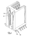
- FIG. 7 is a perspective cross sectional view of a
connector housing of one card edge embodiment of the
disclosed method and apparatus having vertically
staggered contact elements and horizontally staggered
tail portions.
- FIG. 8 is a vertical cross sectional view taken
through the connector housing of FIG. 7.
- FIG. 9 is a cross sectional perspective view of
the connector housing of FIGS. 7 and 8 with the same
shown in a mated position with a card edge and mounted
on a printed circuit hoard.
- FIG. 10 is a perspective cross sectional view of a
plug and socket of an electrical interconnection of one
embodiment of the disclosed method and apparatus having
alternating active and passive type contacts.
- FIG. 11 is a perspective cross sectional view of a
plug and socket of an electrical interconnection
according to one embodiment of the disclosed method and
apparatus having alternating type contacts and a single
channel in which connector halves mate.
- FIG. 12 is a vertical cross sectional view of the
electrical interconnection embodiment of FIG. 11.
- FIG. 13 is a perspective cross sectional view of a
plug and socket of an electrical interconnection
according to one embodiment of the disclosed method and
apparatus having alternating type contacts and two
channels in which connector halves mate.
- FIG. 13A is a perspective cross sectional view of
a plug and socket of an electrical interconnection
according to one embodiment of the disclosed method and
apparatus having alternating mixed passive and active
contacts and two channels in which connector halves
mate.
- FIG. 13B is a vertical cross sectional view of the
electrical interconnection embodiment of FIG. 13A.
- FIG. 14 is a vertical cross sectional view of the
electrical interconnection embodiment of FIG. 13.
- FIG. 15 is a perspective cross sectional view of a
plug and socket of an electrical interconnection
embodiment of the disclosed method and apparatus having
a mixed contact arrangement of passive and active
contacts in alternating configuration and a single
channel in which connector halves mate.
- FIG. 16 is a perspective cross sectional view of a
plug and socket of an electrical interconnection
according to one embodiment of the disclosed method and
apparatus having a mixed contact arrangement of passive
and active contacts in an alternating contact
configuration and having two channels in which
connector halves mate.
- FIG. 16A is a perspective cross sectional view of
a plug and socket of an electrical interconnection
according to one embodiment of the disclosed method and
apparatus having an alternating contact configuration
and having two channels in which connector halves mate.
- FIG. 19 is a cross sectional view of another
embodiment of the disclosed method and apparatus.
- FIG. 22 is a horizontal cross sectional view of
the contact pattern of an offset ribbon contact tail
configuration according to one embodiment of the
disclosed method and apparatus.
- FIG. 23 is a horizontal cross sectional view of a
conventional ribbon contact tail configuration.
- FIG. 24 is a perspective cross sectional view of
an electrical interconnection component according to
one embodiment of the disclosed method and apparatus
having contact tails passing through a plurality of
positioning notches in a "in-line tail" design.
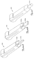
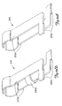
- FIG. 25 shows side and vertical cross sectional
views of a plug and socket component according to one
embodiment of the disclosed method and apparatus,
including positioning notches.
- FIG. 25A is a horizontal cross sectional view of a
contact tail member and positioning notch design
according to one embodiment of the disclosed method and
apparatus.
- FIG. 25B is a horizontal cross sectional view of a
contact tail member and positioning notch design
according to another embodiment of the disclosed method
and apparatus.
- FIG. 26 is a perspective cross sectional view of
one component of an electrical interconnection
according to the disclosed method and apparatus having
contact tails which pass through a plurality of
positioning notches in a "multi-level tail"
configuration.
- FIG. 27 shows side and vertical cross sectional
views of the electrical interconnection component
embodiment of FIG. 26, including positioning notches.
- FIG. 28 is a perspective cross sectional view
showing spatial arrangement of contacts and contact
tails according to two embodiments of the disclosed
method and apparatus having in-line and multi-level
tail configurations respectively.
- FIG. 29 shows vertical and horizontal cross
sectional views illustrating spatial arrangement of in-line
and multi-level contact tail exit designs
according to two embodiments of the disclosed method
and apparatus.
- FIC. 29A is a perspective cross sectional view of
a card edge connector according to one bi-level tail
embodiment of the disclosed method and apparatus.
- FIG. 29B is a cross sectional views of a typical
inline tail member and a bi-level tail member according
to one embodiment of the disclosed method and
apparatus.
- FIG. 30 is a planar cross sectional view of the
in-line tail exit configuration according to the
embodiment of FIG. 29 with electric field distribution
lines illustrated.
- FIG. 31 is a planar cross sectional view of the
multi-level tail exit configuration of the embodiment
of FIG. 29 with electric field distribution lines
illustrated.
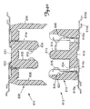
- FIG. 32 shows simplified vertical and horizontal
views of electrical interconnection components
according to two embodiments of the disclosed method
and apparatus having in-line and multi-level tail
designs configured in a two row tail configuration.
- FIG. 33 shows simplified horizontal and vertical
views of electrical interconnection components
according to two embodiments of the disclosed method
and apparatus having in-line and multi-level tail
designs configured in a one row tail configuration.
- FIG. 33A is a cross sectional view illustrating
spatial arrangement of a tri-level tail exit design
according to one embodiment of the disclosed method and
apparatus.
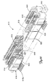
- FIG. 34 is a perspective view of a component of an
electrical interconnection device according to one
embodiment according to one embodiment of the disclosed
method and apparatus having multi-level tail
configuration and showing positioning notches.
- FIG. 35 shows vertical cross sectional views of
components of an electrical interconnection system
according to five embodiments of the disclosed method
and apparatus having a bi-level configuration with a
cap, an in-line plastic bi-level lead, a bi-level
configuration with no cap present, a bi-level
configuration with lead guides, and an in-line
configuration.
- FIG. 36 shows side cross sectional views of the
component configurations of FIG. 35.
- FIG. 36A is a horizontal cross sectional view of a
contact tail member and positioning notch design
according to one embodiment of the disclosed method and
apparatus.
- FIG. 36B is a horizontal cross sectional view of a
contact tail member and positioning notch design
according to another embodiment of the disclosed method
and apparatus.
- FIG. 36C is a horizontal cross sectional view of a
contact tail member and positioning notch design
according to another embodiment of the disclosed method
and apparatus.
- FIG. 36D is a perspective cross sectional view of
a connector component according to one embodiment of
the disclosed method and apparatus.
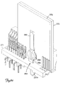
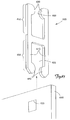
- FIG. 37 is a perspective cross sectional view of a
card edge connector component of an electrical
interconnection system according to one embodiment of
the disclosed method and apparatus having three anchor
structures disposed on the component housing for
anchoring the connector to a printed circuit board.
- FIG. 38 is a perspective cross sectional view of
the connector component embodiment of FIG. 37.
- FIG. 39 is an enlarged perspective view of one end
of the board attachment side of the card edge connector
housing embodiment of FIGS. 37 and 38 showing one
anchor structure in more detail.
- FIG. 40 is an enlarged cross sectional view of an
anchor structure positioned on the board attachment
side of the card edge connector housing embodiment of
FIGS. 37 and 38.
- FIG. 41 is a vertical cross sectional view of an
anchor structure attached to a connector housing
according to one embodiment of the disclosed method and
apparatus.
- FIG. 42 is a vertical cross sectional view of an
anchor structure attached to a connector housing and
engaged in a printed circuit board according to one
embodiment of the disclosed method and apparatus.
- FTG. 43 is a side view of a connector housing
having three anchor structures according to one
embodiment of the disclosed method and apparatus and
showing two anchor structures engaged with a printed
circuit board having an exaggerated concave condition.
- FIG. 44 is a side view of a connector housing
having three anchor structures according to one
embodiment of the disclosed method and apparatus
showing all three anchor structures engaged with
printed circuit board having an exaggerated concave
condition.
- FIG. 45 is a side view of a connector housing
having three anchor structures according to one
embodiment of the disclosed method and apparatus
showing one anchor structure engaged with a printed
circuit board having an exaggerated convex condition.
- FIG. 46 is a side view of a connector housing
having three anchor structures according to one
embodiment of the disclosed method and showing
engagement of all three anchor structures with the
printed circuit board of FIG. 45 having an exaggerated
convex condition.
- FIG. 47 is a cross sectional view of an anchor
structure according to one embodiment of the disclosed
method and apparatus showing typical dimensional
ranges.
- FTG. 48 is a perspective cross sectional view of
an electrical interconnection component having an
anchor structure according to one embodiment of the
disclosed method and apparatus.
- FIG. 49 is a perspective cross sectional view of a
card edge connector component having a separable latch
mechanism and anchor structure according to one
embodiment of the disclosed method and apparatus .
- FIG. 50 is a perspective cross sectional view of a
card edge connector component having a connector latch
portion and a printed circuit board having a
corresponding receiving slot and profile recesses with
the same disposed in position for interconnection.
- FIG. 51 is a perspective cross sectional view of
the connector housing and printed circuit board of FIG.
50 showing the same disposed in mated condition.
- FIG. 52 is a perspective view of a card edge
connector housing and a printed circuit board having a
separable latch configuration according to one
embodiment of the disclosed method and apparatus and
showing the same disposed in position for
interconnection.
- FIG. 53 is an enlarged perspective view of a
printed circuit board having a receiving slot and
profile recess configuration according to one separable
latch embodiment of the disclosed method and apparatus.
- FIG. 54 is a simplified side view of a printed
circuit board with tooling holes and a latch opening
disposed therein according to one embodiment of the
disclosed method and apparatus.
- FIG. 55 is a simplified side view of the printed
circuit board of FIG. 54 showing the circuit board with
contacts disposed thereon according to one embodiment
of the disclosed method and apparatus.
- FIG. 56 is a simplified side view of the printed
circuit board of FIGS. 54 and 55 showing the printed
circuit board following routing of a receiving slot,
board edges, and alignment notches according to one
embodiment of the disclosed method and apparatus.
- FIG. 57 is a perspective cross sectional view of a
one millimeter pitch card edge connector having a
conducting separable latch mechanism according to one
embodiment of the disclosed method and apparatus.
- FIG. 58 is a perspective view of a printed circuit
board having conducting latch profile recesses
according to one embodiment of the disclosed method and
apparatus.
- FTG. 59 is a perspective cross sectional view of a
card edge connector and corresponding card edge
configured according to one conducting latch embodiment
of the disclosed method and apparatus with the same
disposed in position for interconnection.
- FIG. 59A is a perspective view of a conducting
separable latch mechanism according to one embodiment
of the disclosed method and apparatus.
- FIG. 59B is a perspective view of a conducting
separable latch mechanism according to another
embodiment of the disclosed method and apparatus.
- FIG. 59C is a perspective view of a conducting
separable latch mechanism according to another
embodiment of the disclosed method and apparatus.
- FIG. 59D is a perspective view of a conducting
separable latch mechanism according to another
embodiment of the disclosed method and apparatus.
- FIG. 59E is a perspective view of a conducting
separable latch mechanism according to another
embodiment of the disclosed method and apparatus.
- FIG. 60 is a perspective cross sectional view of a
connector housing and printed circuit board according
to one conducting separable latch embodiment of the
disclosed method and apparatus with the same disposed
in mated position.
- FIG. 60A is a perspective view of a circuit board
configured with a receiving slot and dual profile
recesses according to one embodiment of the disclosed
method and apparatus.
- FIG. 60B is a perspective view of a circuit board
configured with an oblong profile recess and extended
receiving slot according to one embodiment of the
disclosed method and apparatus.
- FIG. 60C is a perspective view of a circuit board
configured with an oblong profile recess according to
one embodiment of the disclosed method and apparatus.
- FIG. 60D is a perspective view of a circuit board
configured with an oblong profile recess and buried
conductive layers according to one embodiment of the
disclosed method and apparatus.
- FIG. 61 is an enlarged perspective view of a
connector housing with an attached straddlemount
attachment clip according to one embodiment of the
disclosed method and apparatus.
- FIG. 62 is a perspective cross sectional view of a
connector housing with an attached straddlemount clip
engaged with a printed circuit board according to one
embodiment of the disclosed method and apparatus, with
typical dimensions indicated.
- FIG. 62A is a perspective cross sectional view of
a connector housing similar to the embodiment shown in
FIG. 62.
- FIG. 63 is a simplified side view of a connector
housing with attached straddlemount attachment clips
and a printed circuit board configured to receive the
straddlemount attachment clips according to one
embodiment of the disclosed method and apparatus with
the same disposed in position for interconnection.
- FIG. 63A is a perspective view of the printed
circuit board embodiment of FIG. 63.
- FIG. 64 is a perspective cross sectional view of a
connector housing and an attached straddlemount
attached clip according to another embodiment of the
disclosed method and apparatus.
- FIG. 65 shows perspective views of three possible
straddle mount attachment clip embodiments of the
disclosed method and apparatus.
- FIG. 66 is a horizontal cross sectional view of an
alternating contact foot print configuration according
to one straddle mount attachment embodiment of the
disclosed method and apparatus.
- FIG. 67 is a perspective view of a contact element
having alternating contact retention features according
to one embodiment of the disclosed method and
apparatus.
- FIG. 68 is an enlarged perspective cross sectional
view of a connector housing having contact elements
with alternating contact retention features according
to one embodiment of the disclosed method and
apparatus.
- FIG. 68A is an enlarged perspective cross
sectional view of a connector housing having contact
elements with conventional contact retention features
according to one embodiment of the disclosed method and
apparatus.
- FIG. 69 is a vertical cross sectional view of a
connector housing having contact elements with
alternating contact retention features according to one
embodiment of the disclosed method and apparatus.
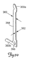
- FIG. 70 is a perspective view of a rotated contact
element according to one embodiment of the disclosed
method and apparatus.
- FIG. 71 is a side view showing spatial positioning
of rotated contacts according to one embodiment of the
disclosed method and apparatus.
- FIG. 72 is a perspective cross sectional view of a
connector housing having rotated contacts and disposed
on a printed circuit board according to one plated
through hole embodiment of the disclosed method and
apparatus.
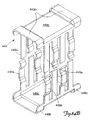
- FIG. 73 is a perspective cross sectional view of a
connector housing having rotated contacts according to
one embodiment of the disclosed method and apparatus.
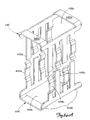
- FIG. 74 is a perspective cross sectional view of a
card edge connector housing having rotated contacts
according to one embodiment of the disclosed method and
apparatus.
- FIG. 75 is a perspective view of a card edge
connector component having rotated contacts and a card
edge according to one embodiment of the disclosed
method and apparatus with the same disposed in position
for interconnection.
- FIG. 76 is a perspective cross sectional view of a
connector housing having power contacts with a "T-shaped"
based and surface mount foot portions according
to one embodiment of the disclosed method and
apparatus.
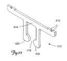
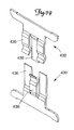
- FIG. 77 is a perspective view of a "T-shaped"
contact according to one embodiment of the disclosed
method and apparatus.
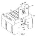
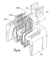
- FIG. 78 is a perspective cross sectional view of a
two piece electrical interconnection having a plug and
socket with "T-shaped" power contacts according to one
embodiment of the disclosed method and apparatus with
the same disposed in position for interconnection.
- FIG. 79 is a perspective view showing mating "T-shaped"
power contacts of the embodiment of FIG. 78
with the same shown disposed in position for
interconnection.
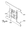
- FIG. 80 is a perspective view of "T-shaped" power
contacts of the embodiment of FIG. 78 with the same
disposed in mated condition.
- FIG. 81 is a perspective view of "T-shaped"
contact structures having two conducting fingers
according to one embodiment of the disclosed method and
apparatus with the same disposed in position for
interconnection.
- FIG. 82 is a perspective view of a "T-shaped"
power connector having three conducting fingers
according to one embodiment of the disclosed method and
apparatus.
- FIG. 83 is a perspective cross sectional view of
"T-shaped" power contacts having four conducting
fingers according to one embodiment of the disclosed
method and apparatus with the same disposed in position
for interconnection.
- FIG. 84 is a perspective view of power contacts
having four conductor fingers according to one
embodiment of the disclosed method and apparatus with
the same disposed in position for interconnection.
- FIG. 84A is a perspective view of power contacts
having two rows of four conductor fingers according to
one embodiment of the disclosed method and apparatus
with the same disposed in position for interconnection.
- FIG. 84B is a perspective view of power contacts
having two rows of four conductor fingers according to
another embodiment of the disclosed method and
apparatus with the same disposed in position tor
interconnection.
- FIG. 85 is a perspective cross sectional view of
a plug and socket having separate power modules
according to one mezzanine embodiment of the disclosed
method and apparatus.
- FIG. 86 is a perspective cross sectional view of a
connector housing having a separate power module and a
printed circuit board according to one straddlemount
embodiment of the disclosed method and apparatus with
the same disposed in mated condition.
- FIG. 87 is a perspective view of a "U-shaped"
power contact and a printed circuit board according to
one straddlemount embodiment of the disclosed method
and apparatus with the same disposed in position for
interconnection.
- FIG. 88 is a perspective view of the socket of an
electrical interconnection according to the present
invention.
- FIG. 89 is a perspective view of the plug of an
electrical interconnection according to the present
invention.
- FIG. 90 is a vertical cross sectional view taken
through the socket of FIG. 88 and the plug of FIG. 89
with the same disposed in position for interconnection.
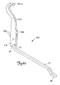
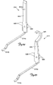
- FIG. 91 is a schematic view showing the foot print
of the socket or plug according to the embodiment of
FIG. 90.
- FIG. 92 is a vertical cross sectional view of a
socket and plug of a first modification.
- FIG. 93 is a schematic view of the foot print of
the socket or plug according to FIG. 92.
- FIG. 94 is a perspective view of a passive contact
element.
- FIG. 95 is a perspective view of an active contact
element.
-
DESCRIPTION OF ILLUSTRATIVE EMBODIMENTS
-
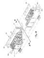
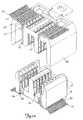
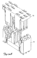
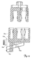
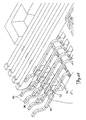
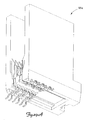
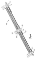
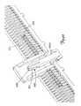
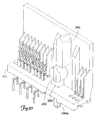
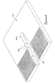
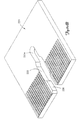
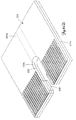
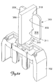
As a starting point of reference, FIGS. 1A and 1B
illustrate one embodiment of an interconnection system
according to the disclosed method and apparatus. FIG.
1A illustrates a socket housing component 16 and FIG.
1B illustrates a mating plug housing component 26 for
interconnection with socket housing 16. As illustrated
in FIG. 1A, socket 16 has a housing body comprising a
base 1 and three spaced parallel wall members 1a
positioned on one side of base 1. As illustrated in
FIG. 1B, plug 26 has a housing body comprising a base 2
and two wall members 2a in spaced parallel position to
receive walls 1a of socket 16 and two exterior wall
members forming housing shroud 27. Active contact
elements 12 and corresponding passive contact elements
13 are provided within each connector housing component
16 and 26. In FIG. 1, section A-A of FIG. 1A and
section B-B of FIG. 1B are presented in a position
prior to connector mating. In FIG. 2, section A-A of
FIG. 1A and section B-B of FIG. 1B are shown in mated
position. As shown in FIG. 1, contact tails 21 are
coplanar. FIG. 1C illustrates cross sectional views
similar to those found in FIG. 1 except for an
embodiment of the socket 16 and plug 26 apparatus
having multi-level contact tails 21. The use of multi-level
contact tail exit designs is discussed in more
detail below.
Two-Piece Connectors Having Multiple Contact Rows and
Contact Channels
-
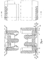
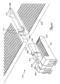
Typical two piece connectors utilize a T-shaped
plug which inserts into a U-shaped socket. FIG. 1E
illustrates a cross section of such a connector. As
shown in FIG. 1E, a U-shaped socket 4 includes a socket
housing 5 which has side housing walls 5a and 5b. The
housing 5 may be rectangularly elongated such as the
housings shown in FIGS. 1A and 1B. In FIG. 1E, a
single connector channel 7 is formed between the side
housing walls 5a and 5b. Located adjacent to each
housing walls 5a and 5b is a row of contacts. One
contact 4a and one contact 4b of each of the two rows
of contacts are shown in the cross sectional view of
FIG. 1E. The contact rows may be formed so that each
contact is co-planar, or alternatively, as shown in
FIG. 11 a contact row may have a line of contacts that
are staggered such that every other contact of one row
projects further into the connector channel 7.
-
The plug 3 may include a plug housing which has a
central wall 6. The plug housing may also include
optional outer shrouds 6a and 6b as shown by dotted
lines in FIG. 1E. On either side of the central wall 6
connector channels 8 and 9 are formed. If outer
shrouds 6a and 6b are utilized, the connector channels
8 and 9 may be considered enclosed channels (as would
connector channel 7). If outer shrouds 6a and 6b are
not utilized connector channels 8 and 9 may be
considered open channels. In either case, rows of
contacts 3a and 3b are formed adjacent central wall 6
adjacent to the connector channels. As with the socket
4, each row of contacts that contain contacts 3a and 3b
may be a row of co-planar contacts or a row of
staggered contacts such that some contacts may extend
into the channels further than other contacts. Thus,
as shown in FIG. 1E, an interconnection system having a
socket with one connection channel and a plug with two
connection channels is provided
-
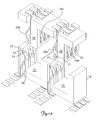
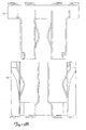
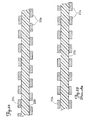
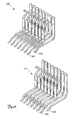
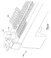
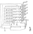
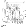
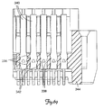
The interconnection system shown in FIGS. 1, 1A,
1B and 1C advantageously provide a plurality of
channels for both the socket and the plug. The use ot
a plurality of channels allows for an increased number
of contacts to be made over a given area for a
connector. Thus, though conventional connectors may
provide only two rows of contacts in a plug or socket,
an interconnection system according to the present
disclosure may utilize three, four, or more contact
rows in each of the plug and socket pieces.
-
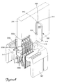
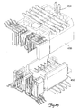
For example, as shown in FIGS. 1A and 1B, a plug
26 has three connector channels 26a and a socket 16
having two connector channels 16a. Further four rows
of contacts (two rows of active contacts 12 and two
rows of passive contacts 13) are provided in the plug
26 and likewise four rows of contacts (two rows of
active contacts 12 and two rows of passive contacts 13)
are provided in the socket 16. Once again the contacts
within each row of contacts may be either co-planar or
staggered into the connector channel regions by varying
amounts.
-
The use of a plurality of connector channels for
both a socket and a plug is not limited to the specific
combination of active and passive contacts as shown,
but may be utilized with other combinations including
all active contacts. Further, though shown primarily
with a two piece interconnection system having one
piece with three connector channels (with four rows of
connectors) mating to a second piece with two connector
channels (with four rows of connectors), although
combinations of a multiple number of channels in both
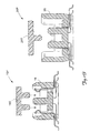
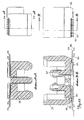
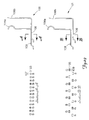
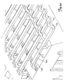
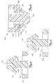
the socket and plug may be utilized. For example, as
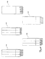
shown in FIG. 1F two variations of multiple connector
channels are shown. Interconnection system 1000
includes housing 1002 which includes three connector
channels 1006 and five rows of contacts 1008 which may
mate with housing 1004 which includes four connector
channels and five rows of contacts 1008. Similarly,
interconnections system 1010 includes housing 1012
which includes three connector channels 1006 and six
rows of contacts 1008 which may mate with housing 1014
which includes four connector channels and six rows of
contacts 1008. A variety of other channel and row
combinations could be used including, for example, two
channel pieces mating to two channel pieces, three
channel pieces mating to three channel pieces, four
channel pieces mating to five channel pieces, five
channel pieces mating to six channel pieces, etc. For
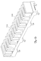
example, FIG. 1D illustrates a interconnection piece
having more than 10 channels 1006. Also, many
combinations of enclosed and open connector channels
may be utilized. Finally, a variety of combinations of
number of contact rows may also be utilized, including
circumstances were one contact row of a plug may engage
two rows of a corresponding socket such that an equal
number of contact rows are not required in a matching
socket and plug.
Contact Support Geometry
-
To address connection reliability problems
inherent in traditional cantilevered active spring
contacts, embodiments of the disclosed method and
apparatus may include a connector housing having a
contact support surface. FIG. 1 shows one embodiment
of a convex arcuate contact support surface 10 adjacent
to a non-deflected cantilevered spring contact element
12. The contact element 12 has a fixed first end 14
anchored in thermoplastic socket connector housing 16.
In FIG. 2 spring contact 12 of FIG. 1 is shown
deflected against arcuate support surface 10 due to
contact with mating contact element 20.
-
In FIG. 2, interaction between the arcuate support
surface and the spring contact has caused the effective
"fixed point" of the spring contact to shift toward the
free second end 18 of the contact. In other words, the
length of spring contact existing between the outward
point of spring contact/support surface interaction
(the "support point") and the end of the contact has
been shortened by deflection of the contact against the
support surface. Thus, the effective length of the
spring contact has been shortened, and the internal
stress present at the second end of the contact
maintained, delivering substantially the same force
over a shorter distance. FIGS. 3 and 4 graphically
illustrate deflection force and internal stresses as a
function of position.
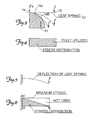
-
As can be seen in FIG. 3, spring contact 12 is
bent or deflected around arcuate support surface 10 by
contact normal force (F). FIG. 4 illustrates internal
stress distribution within the deflected spring contact
of FIG. 3 as a function of position. As shown in
FIG. 4, internal stress is fully utilized from the
fixed end to the free end of spring contact 12, unlike
stress distribution in unsupported cantilever spring
contacts, as illustrated in FIGS. 5 and 6. As the
spring contact 12 of FIGS. 3 and 4 is deflected against
the support surface 10. The support point shifts from
position 14 to position 14a and 14b, as shown in FIG.
3. Thus, an increasingly shortened deflection path is
created between the support point 14 and the free end
18 of the contact. As a result, maximum contact normal
force is essentially maintained at the free end 18 of
the contact 12 as it is bent around the support 10.
The normal force present at the fixed or anchored end
of the contact also remains essentially constant as
contact 12 is deflected around support 10.
-
FIG. 2 is a cross sectional view of two mated
connector components showing deflection of an active
spring contact 12 against a convex arcuate support
structure 10. As shown in FIG. 2, two connector
components are mated; however, an alternative
embodiment may be utilized when connecting a printed
circuit board card edge to a connector component. FIG.
2B is a similar cross sectional view of a card edge
embodiment having a mated card edge 12a and connector
component 12b and showing deflection of an active
spring contact 12 against a convex arcuate support
structure 10. In FIG. 2B, the connector component 12b
may be referred to as a "socket" connector component,
and the card edge 12a may serve as a "plug" component.
-
As shown in FIG. 2, a contact may be configured
with a curved shaped contact free end 18. A
displacement cavity 24 may be provided at the outward
end of a support structure to accept the contact free
end 18 when it is deflected. The backwall of the
cavity provides a pin stop which prevents over
deflection of the contact 12. Because contact normal
force is essentially maintained at the free end of
deflected contact 12 in FIG. 2, constriction resistance
and heat generation are minimized when using this
embodiment of the disclosed design. Because deflected
spring contact 12 is supported by convex arcuate
support surface 10, housing material "creep" and
adverse effects from vibration are also minimized. The
shortened deflection path between the point of support
and the free end of the contact acts to provide greater
contact normal force while at the same time reducing
the possibility of overstressing the contact material
and/or causing contact material permanent deflection.
Therefore, connectors utilizing supported contacts of
the disclosed design may have decreased constriction
resistance, improved longevity, and greater reliability
over previous connector contact designs. Other
advantages of the disclosed method and apparatus may
include the ability to utilize lower strength, but less
costly contact material in a given application.
furthermore, because embodiments of the disclosed
method and apparatus utilize a relatively straight
contact arm and a contact support that is integral to
the connector housing, overall connector width is
essentially the same as a connector employing an
unsupported cantilevered contact. This makes
embodiments of the disclosed method and apparatus
particularly suitable for miniaturization.
-
FIGS. 1, 1A, 1B, 1C and 2 illustrate an embodiment
of a contact profile, contact support surface, and
accompanying displacement cavity that may be
successfully used with the disclosed design.
Advantageously, deflection characteristics and internal
stress distribution may be altered by varying support
and/or contact profile geometry. Besides the convex
arcuate shape illustrated in FIGS. 1 and 2, any support
shape suitable for contacting and supporting a
deflected contact may be employed. For example, as
illustrated in FIG. 6A, other shapes and configurations
for contact support surface 10 may be employed,
including but not limited to, other arcuate shapes
(such as oblong or elliptical), angled linear shapes,
single points, or combinations thereof. Some specific
examples (as illustrated in FIG. 6A) include two line
segments with one segment angled and one straight, two
line segments with both segments angled, three line
segments with all segments angled, three line segments
with one segment straight and two angled, four line
segments with one straight and three angled, one line
segment with one radius, two line segments and one
radius, one radius, and one elliptical surface. In
addition, contacts having both linear and non-linear
profiles may be employed including, but not limited to
those having a linear, arcuate or angled profile. For
example, in one embodiment, a linear contact support
structure may be employed with a contact having a cross
sectional area tapering toward a free end of the
contact in such a way that the effective fixed point
moves toward the free end of the contact with
deflection during mating.
-
Contact ends may also be of any profile suitable
for forming a contact point with another contact
including, but not limited to rounded, arcuate,
pointed, angled, as well as any shape disclosed in the
accompanying illustrations. In addition, contacts
having tapered width and/or thickness, or otherwise
varying cross sectional shape may be employed. For
example, FIG. 67 illustrates a contact element 334
having a tapered width section 331. In addition to the
embodiment illustrated in FIG. 67, contact elements may
be configured with shorter or longer taper sections
and/or located in other areas of a contact (such as a
tapered section that span the length of a contact from
base to tip). Advantageously, by tapering width and/or
thickness of a contact, contact deflection
characteristics and other properties may be varied.
This is possible, in part, because as the width and/or
thickness of a contact is reduced, contact deflection
force is decreased, and vice-versa as a contact
thickness is increased. For example, a contact may be
tapered to have a reduced width and/or thickness toward
the contact tip 331a in order to reduce insertion
force, therefore allowing an increased number of
contact elements in an interconnection system.
Therefore, contact deflection force may be
synergistically optimized by combining a tapered
contact with contact support geometry of the disclosed
method and apparatus. In this way benefits of contact
support geometry (reduced creep, reduced stress
relaxation, thinner contacts, etc.) may be realized
without the necessity of increasing connector insertion
force. By tapering a contact to have a larger width
and/or thickness toward the contact tip, contact
deflection force (and therefore, connector insertion
force), may be increased, if so desired. Variable
and/or multiple contact taper sections are also
possible, to achieve multiple zones of varying
deflection force. Finally contact width may be tapered
in such a way to interact geometrically with contact
support geometry of the disclosed method and apparatus,
such that changes in effective length of a contact may
be varied, for example, to occur more rapidly or less
rapidly as a function of deflection.
-
Likewise, a displacement cavity may be of any
suitable geometry for accepting a shaped contact end,
or may not be necessary where sufficient clearance
exists without the presence of a cavity. In addition,
a contact support structure of the disclosed design may
be constructed of any material suitable for providing
support to a deflected contact. For example, the same
material as the associated connector housing (such as
plastic or ceramic) may be employed, or a support
structure may be constructed of a different material
than the connector housing. Finally, benefits of the
contact support structure of the disclosed method and
apparatus may be obtained with connector configurations
employing active contacts that mate with other active
contacts, as well as in those configurations where
active contacts mate with passive contacts.
Vertically Staggered Contact Element Configuration
-
For both card edge and two piece connector
applications, it is often desirable to utilize staged
or sequential mating of conducting elements.
Staged/sequential mating generally refers to placement
of conducting elements such that all conducting
elements do not mate simultaneously, but rather, as two
connectors are brought together some conducting
elements engage before others engage. For example,
sequential mating of conductor elements may be needed
for completing ground, signal, and/or power circuits in
specific order. Sequential mating also tends to lower
the maximum insertion force required for mating because
only a portion of contact element peaks are being
engaged at one time. Therefore, in one embodiment of
the disclosed method and apparatus shown in FIG. 7, the
spring member and/or wiping portions of a connector/s
are vertically staggered, as are the associated contact
supports. This vertically staggered configuration is
illustrated with aid of hidden lines in FIG. 8. As
shown in FIG. 8, two levels of contact spring elements
are present, upper contact spring elements 30 and lower
contact spring elements 32. Also present, are two
levels of contact supporting structures, upper level
contact supporting structures 34, and lower level
contact supporting structures 36.
-
It should be noted that vertically staggered
connector configurations wilt typically employ a
horizontal stagger of upper contact tail portions 38
and lower contact tail portions 40 as shown in FIGS. 7-9.
Horizontal staggering enables the physical and
electrical lengths of the interconnection paths to be
the same regardless of position in the connector. In
line with this, FIG. 7 shows a vertically and
horizontally staggered card edge embodiment. FIG. 9
also shows a vertically and horizontally staggered card
edge embodiment, this time with mating printed circuit
board 42 inserted. Although FIGS. 7-9 illustrate the
vertically staggered contact concept in use with a card
edge embodiment having rotated contacts, it will be
apparent with benefit of the present disclosure that
the vertically staggered contact/supporting structure
combination may be used with other types of mating
systems including, but not limited to a standard style
card edge or two-piece connector system. In addition,
benefits of the vertically staggered contact embodiment
may be realized with virtually any type of cantilevered
spring contact having a variety of cross sectional
profiles including, but not limited to, "ribbon" type
contacts.
Alternating and Horizontally Staggered Contact Designs
-
Embodiments of the disclosed method and apparatus
may be practiced using offset ribbon type contacts,
and/or other types of contacts, such as rotated
contacts. FIG. 1 shown one alternating contact
embodiment in which contacts alternate in lateral
position on opposite sides of wall members 2a of plug
housing component 26. This alternation is evidenced by
visibility of the bases of end passive contacts 20a and
non-visibility of the bases of end active contacts
positioned on opposite sides of center walls 2a when
viewed in the same side cross sectional plane of FIG.
1. FIGS. 13 and 14 illustrate another alternating
contact embodiment in perspective and cross sectional
views, respectively. In FIGS. 13 and 14, contacts 20b
and 20c positioned on outer sides of center walls 2a of
plug housing 72 may be seen to be laterally offset from
contacts 20d and 20e positioned on inner sides of walls
2a, respectively. Contacts 20d may also be seen to be
laterally offset from contacts 20e in the embodiment of
FIRS. 13 and 14. However, contacts 20d and 20e may be
alternatively configured to be on the same centerline
as may all contacts 20b-20e in other embodiments.
-
FIGS. 22 and 23 show horizontal cross sectional
views of contact patterns of an offset ribbon tail
configuration of the disclosed method and a
conventional pattern of the prior art, respectively.
In FIG. 22 contacts 22a may be seen to be disposed in
offsetting relationship on opposite sides of connector
center wall 22b, thereby forming an alternating contact
embodiment. In contrast, FIG. 23 illustrates a
conventional contact configuration of the prior art in
which contacts 23a may be seen to be disposed directly
opposite each other on opposing sides of connector
center wall 23b. In the manner illustrated,
alternating contacts may be disposed on opposite sides
of connector walls in any number of connector
configurations, for example on connectors having more
than one channel and/or walls, and disposed on each
half of a mating connector component combination.
-
FIG. 10 is a perspective cross sectional view of
one embodiment of an unmated two piece connector
according to the disclosed method and apparatus. The
connector embodiment illustrated in FIG. 10 is a ribbon
system in which both plug 26 and socket 16 housings
contain four rows of alternating active and passive
type contacts. In this configuration, the center rows
of both plug 26 and socket 16 typically contain one
additional or one fewer contact per row over the
exterior rows which surround them. This offset or
alternating contact configuration allows construction
of a finer pitch, higher density, and higher pin count
connector products, as described below.
-
FIG. 1 is a cross sectional representation of an
alternating contact design. Although this embodiment
utilizes connectors having four rows of contacts, the
alternating contact design may be practiced in a
variety of other configurations having greater or fewer
number of rows of contacts, for example, six rows of
contacts as illustrated in FIG. 33A. In addition, FIG.
1 also illustrates a connector plug having an optional
housing shroud 27 with an alignment notch 29. It will
be understood with benefit of the present disclosure
that the method and apparatus of the present invention
may be successfully practiced without housing shroud
27. However, housing shroud 27 is typically employed
for many reasons, including to provide pin protection,
component alignment, mechanical stability, rigidity,
resistance to longitudinal component bow or twist,
and/or to provide polarization during connector mating.
Additionally, keyed shrouds may be utilized to allow
selective mating only between specific types of plugs
and sockets.
-
Among the advantageous features offered by the
embodiments illustrated in FIGS. 1 and 10 are the
mixture of active 12 and passive 13 contacts, and the
offset or alternation of these contacts. The mixture
of active and passive contacts provides a density
increase over existing methods and designs by providing
greater space and materials utilization which may lead
to a lower applied cost. This is in part because
relatively flat passive contacts take up less space
than relatively bowed (or otherwise shaped) active
spring contacts. By mixing active and passive
contacts, mechanical and thermal expansion stresses are
distributed equally on both connector housings 16 and
26. This results in superior system reliability and
allows an increased connector housing link, translating
into a higher pin count potential. In addition, this
configuration provides improved uniformity of
electrical path length through the connector housing,
leading to greater electrical performance of a system,
regardless of position in the connector (meaning row 1
vs. row 2 vs. row 3 vs. row 4). Therefore, the mixture
of active and passive contacts provides density, pin
count, mechanical performance, electrical performance,
reliability, and cost benefit improvements (such as a
improvements in the amounts and types of metals
utilized).
-
The second feature provided by the embodiments
illustrated in FIGS. 1 and 10 is the offset or
alternating contact pattern. This alternating contact
pattern provides advantages in the assembly of very
fine pitch connector systems. As shown in FIGS 10 and
67, the contact tail 21 and surface mount foot 23 of
the systems may be centered on contact base 13f
providing a measurable area or land 25 (for assembly
equipment) on each side of the contact tail 21 for
which assembly equipment may locate and press a contact
into a housing. With a contact tail 21 centered on all
contacts 12 and 13 and the contact bases 13f offset
one-half contact position between an inner row and
outer row, the surface mount foot portion 23 of an
inner row contact may pass between the contact base
area 13f of the neighboring outer row contacts and exit
to the board as shown in FIGS 1 and 10. Therefore, the
resulting board attachment process and circuit routing
may be simplified. It will be understood with benefit
of the present disclosure that in addition to those
embodiments illustrated, alternating contact patterns
may be employed without mixed active and passive
contacts.
-
Finally, as may be seen in FIGS. 1, 1C and 2,
interior walls 15 of plug housing 26 may be
manufactured thinner than corresponding exterior walls
11 of socket housing 16. This is made possible in the
illustrated embodiment by offsetting mating forces
created by deflection of active plug contacts 12
against contact support structures 10 located on
interior sides of interior walls 15 of plug housing 26,
and by contact of active socket contacts 12 against
contact support structures 10 located on interior sides
of interior walls 15 of plug housing 26, and by contact
of active socket contacts 12 with passive plug contacts
13 located on exterior sides of interior walls 15 of
plug housing 26. Accordingly, thickness of interior
walls 15 of plug housing 26 may be dictated only by
need for dielectric insulating capacity and contact
support structure geometry, allowing further reduction
in connector dimensions. Such an advantage is not
possible with conventional non-alternating contact
designs which may require metal housings or special
support features for connector integrity. Nor would
such an advantage be fully realised using conventional
cantilever beam spring contacts without the presence of
contact support structures 10. This is because
conventional active contacts are unsupported and
therefore not capable of transferring a reactive force
to counterbalance forces acting on passive contacts 13
therefore, for example, requiring wall 15 to be
thicker.
-
The offset or alternating contact configuration of
the disclosed method and apparatus provides increased
contact support over conventional contact
configurations having the same effective contact pitch.
In addition to structural and mechanical advantages,
this alternating contact configuration provides
superior electrical isolation from adjacent contacts in
the mating area and in the tail exit area, resulting in
more reliable electrical performance with increased
dielectric withstanding strength, insulation
resistance, and the like, in addition to providing high
speed performance.
-
The contact elements may be disposed within a
connector housing in a variety of different ways. For
example, FIGS. 11 and 12 disclose a contact
configuration having one major grove or channel 70 in
which connector halves 72 and 74 mate, while FIGS. 13
and 14 illustrate another embodiment having two major
groves or channels 70 in which connector halves 72 and
74 mate. In FIG. 11, contacts 76 are horizontally
staggered along each sidewall of one major mating
channel 70 as shown in cross sectional view in FIG. 12.
By contrast, in FIG. 13 contacts 76 alternate within
each channel 70 in an alternating manner as previously
described, as shown in cross section view in FIG. 14.
Advantageously , in both alternating and horizontally
staggered contact configurations, a mixed contact
arrangement of passive and active contacts may be
utilized (as illustrated in FIGS. 13A, 13B, 15, and
16).
-
It will also be understood with benefit of the
present disclosure that a horizontally staggered
contact configuration (such as that illustrated in
FIGS. 11 and 12), and an alternating configuration
(such as that shown in FIGS. 13 and 14) may each be
employed in a variety of different connector
configurations in addition to those illustrated. For
example, horizontally staggered contact arrangements
may be employed with connector components having
differing numbers of channels and/or with connector
components that also employ alternating contact
designs. Among the many possible ways that
horizontally staggered and alternating contact
configurations may be combined are as separate contact
configurations disposed on separate channel sidewalls,
or as a "hybrid" mixture in which horizontally
staggered contacts located on one side of connector
wall are deployed in an alternating contact arrangement
with other horizontally staggered contacts disposed on
the opposite side of the same connector wall.
-
FIGS. 11, 12, 13, and 14 illustrate connector
designs in which the contacts are loaded from the
bottom, and FIGS. 13A, 13B, 15 and 16 illustrate
connector designs in which contacts are loaded from the
top or separable side. It will be understood with the
benefit of this disclosure that very similar connector
designs are possible in which the contacts are loaded
from the bottom, such as that shown in FIG. 10. It
should be noted that FIGS. 10, 15 and 16 illustrate
contact support configurations with an arcuate support
surface as previously described. It will be understood
with the benefit of this disclosure that the
alternating contact designs may be successfully
practiced with or without the support. Illustrating
just one of many other possible connector housing and
contact element embodiments, FIG. 19 shows a connector
component 70e having contact tails 70a configured in a
right angle tail exit design for connection with board
70c. In FIG. 19, connector component 70e is secured to
board 70c by means of anchor post 70b.
-
in the embodiments illustrated in FIGS. 11-14,
each contact tip 71 is configured with a stepped or
bent shape that is "buried" or "captured" within a
corresponding housing notch 73 formed in connector
halves 72 and 74 by a closed cavity end or molded cap
77. By so capturing contact tips 71 in notches 73,
contact alignment is preserved, and contact tips 71 are
constrained and prevented from deflecting or moving
into channels 70 where contacts 76 may become bent or
crushed during connector mating. In FIGS. 15, 16, and
16A an alternative way of protecting and aligning
contact tips according to another embodiment of the
disclosed method and apparatus is illustrated. In this
embodiment contacts 76 have "T-shaped" contact tips 71
that contact or interact with a raised area or ledge
79a disposed on housing cavity walls 79 in such a way
that contact tips 71 are substantially constrained,
protected, and aligned without the type of cap 77 shown
in the embodiments of FIGS. 11, 12, 13, and 14. FIGS.
13, 13A, 15 and 16 show "T-shaped" contact tips 71 and
mating cavity ledges 79a in connector embodiments not
having contact support structures. However, this
configuration is typically and advantageously used with
embodiments of the disclosed method and apparatus
having contact support structures. Not only does the
absence of cavity caps allow the creation of a shorter
and more compact connector housing, but also simplifies
molding by eliminating the need to create a cavity carp.
This is particularly advantageous with regard to
connector housings having contact support structures
because limitations of matching equipment typically
prevent the formation of support structure shapes when
caps are present.
-
It will be understood with benefit of the present
disclosure that a contact tip and corresponding cavity
wall and ledge shape may be of other geometries
suitable for protecting and aligning the contact tip
including, but not limited to T-shapes having other
dimensions and L-shapes that interact with only one
cavity wall.
Tail Design
-
The disclosed interconnection systems and designs
may be practiced with connectors having a variety of
tail exit configurations. These configurations may
include configurations having positioning notches for
aligning and/or retaining contact tails. In the
embodiment illustrated in FIGS. 24 and 25, contact
tails 80 are all coplanar for a distance parallel to
the connector base 82 and remain such as they pass
through a plurality of positioning notches 84 toward
the edge of the insulating housing or body 86 in what
may be referred to as an "inline tail" design.
Positioning notches 84 may also be configured as
grooves, slots, openings, recesses, passages, teeth, or
the like. Each positioning notch 84 receives a
corresponding conducting contact feature 80 as shown in
FIGS. 24 and 25. Each positioning notch 84 may have a
substantially parallel side with a taper, draft, or
angle 84a as shown in FIG. 25A and may be present on
each connector component 16 and 26. When present,
taper 84a is for injection molding notch features 84
into a housing sidewall, and for providing a lead-in
feature for a conducting tail portion 80 that will
facilitate alignment and entrance of the tail portion
80 into notches 84. FIG. 25B illustrates and
alternative embodiment having notches 80 that lack
taper 84a. Once a conducting tail member 80 is
inserted into a corresponding notch 84, the notch 84 is
designed to hold the tail member 80 in a desired
position during shipping and until the connector is
attached to a printed circuit board.
-
Allowing the use of positioning or retention
notches discussed above, is a stepped surface mount
("SMT") tail configuration illustrated in FIGS. 24 and
25. This configuration enables a retention notch 84 to
be created on the housing to receive, hold, and align a
surface mount contact during transportation. As shown
in connector component sections A-A and B-B of FIG. 25,
a flat portion 89 may be provided that is designed to
supply increased strength for the solder joint of a
surface mount contact. A "step" 88 may be supplied
that serves to provide an opening or clearance between
the connector housing and the printed circuit board in
which material remnants from the board attachment
process may be cleaned away following physical
soldering of a connector to a board. The step 88
enables a substantial solder heel to be formed during
the soldering process on the outermost portion of the
radius nearest the board. A solder fillet will
typically be formed during the soldering process on the
sides and end of the flat portion 89 on the stepped
tail. In one embodiment of the disclosed method and
apparatus, the angle between the contact base 87 and
the contact tail 80 may be formed at less than a 90°
interior angle. In this case, when a contact is
assembled into a housing, the contact tail 80 will be
aligned to the notch 84 on the connector sidewall and
will be held there via an upward pressure created by a
cantilever force resulting from interference with the
connector housing 82 which acts to mechanically open
the angle between the contact base 87 and the contact
tail 80 to about 90° during the assembly process. Once
a contact tail 80 is engaged into a positioning notch
84, the strength of the surface mount foot portion is
substantially increased and the lateral and
longitudinal positioning (i.e., in the X-Y position
between adjacent contacts and along the axis of the
contact tail) is more likely to be preserved. The
vertical positioning of a contact tail 80 may be
controlled by varying the seating depth of a contact
base 87. Using this method, a completely planar set of
contacts may be provided, thereby increasing the
capability of a board attachment.
-
Advantageously, when the alternating contact
embodiment of the disclosed method and apparatus is
combined with a step SMT tail design centered in a
positioning notch, three dimensional packaging of the
contacts in a manner which expands the distance between
an adjacent contact tail and solder joint is enabled.
The net effect is that solder bridging is substantially
minimized.
-
In the practice of the disclosed method and
apparatus, a "multi-level tail" design embodiment may
also be employed with or without the stepped tail
design to achieve high interconnection density and to
provide other benefits, such as structural integrity
and signal clarity. A multi-level tail design also
offers increased manufacturing process capability with
respect to contact stamping and forming operations
while at the same Lime maintaining a relatively low
profile and low total product cost. As an example, a
"bi-level tail" embodiment is illustrated in FIGS. 26
and 27, in perspective and cross sectional views,
respectively. In this embodiment, two layers of
electrically conducting tails are provided, an upper
tail layer 90 and a lower tail layer 92, thus providing
the "bi-levels." As shown in FIGS. 26 and 27, each of
these layers are disposed substantially parallel to one
another. In the bi-level tail embodiment illustrated
in FIGS. 26 and 27, each bi-level tall is conducting
and has a generally planar portion 94 coupled to a
stepped surface mount foot portion 96 which also has a
generally planar portion 98. Although the planar
portions 94 of the conductors 90 and 92 are illustrated
to be planar with one another, they may be adjusted
using the method described above for "stepped contact"
designs.
-
FIG. 28 illustrates a comparison of an in-line
tail design 100 and a multi-level tail design (bi-level
in this example) 101. As shown in FIG. 28, both inline
tail configuration 100 and bi-level tail configuration
101 have longitudinally adjacent tails 102 and 104.
However, the bi-level tail 102 configuration increases
separation between adjacent contacts due to both
longitudinal and vertical separation. Although the
overall height may be increased in comparison with the
inline tail embodiment 100, the separation created by
the bi-level tail design 101 substantially reduces
cross talk between conducting tail portions. Added
clearance provided by the bi-level tail embodiment 101
also allows increased tail width which, in turn,
increases current capacity and cooling. In addition,
increased tail width allows the tails to be
mechanically stronger and the manufacturing process
capability to be increased.
-
As mentioned above, the bi-level tail invention
achieves reduction in cross talk by providing contact
tail row separation. Assuming a one ground to one
signal ratio for comparing inline to bi-level tail
configurations, FIGS. 28 and 29 illustrate lines tail
exit designs for inline 100 and bi-level 101 tail
designs respectively. In these figures, ground lines
are depicted with a label of "G" and signal lines are
depicted with a label of "S". FIG. 28 shows standard
inline tail geometry 100 in perspective view and FIG.
29 shows contacts 106a and 106b, and planar tail
portion 108 in cross section. In these figures, ground
lines are depicted with a label of "G" and signal lines
are depicted with a label of "S". The ground and
signal tail designations herein are merely illustrative
and which tails are signal lines or ground lines may
vary.
-
FIGS. 30 and 31 represent Sections A-A and B-B of
FIG. 29, respectively, and include electric field
distribution lines for a GGSSGG arrangement to
illustrate cross talk effects for both inline and bi-level
tail configurations. As shown in FIG. 30, in an
inline tail configuration, a quiet line 114 may be
positioned directly between a driven line 116 and a
ground line 118, creating a potential for cross talk
between the driven and quiet lines as shown. This is a
typical result of a quiet line 114 being positioned
directly between a driven line 116 and the next nearest
ground 118. In this regard, section A-A shows a
resulting electric field distribution for a GGSSGG
arrangement.
-
However, as shown in FIG. 31, in a bi-level tail
configuration, a quiet line 110 adjacent to a driven
line 112 is not positioned directly between the driven
line 112 and its next-nearest ground 113, reducing the
potential for cross-talk. Additionally, in the
bi-level tail embodiment of FIG. 31, distance between
quiet lines 112 and driven lines 113 is greater than
that provided by an inline tail configuration, further
reducing the potential and/or magnitude of cross talk.
It should be noted that contact tails connected to
contacts 106a positioned toward the exterior of a
connector housing are typically positioned on an upper
contact tail row and contact tails connected to
contacts 106b positioned toward the interior of a
connector housing are typically positioned on a lower
contact tail row as shown in FIG. 29. This
configuration maximizes separation between contact
tails because upper contact tail members are not
"crossed" (or located on the same horizontal plane at a
corresponding vertical position) at any point by lower
contact tail members.
-
As shown in the sectional views of FIG. 29,
thickness of an inline conducting tail element 103 is
typically equivalent to the thickness of a bi-level
conducting tail element 105. However, the geometry of
a bi-level tail configuration allows for a bi-level
tail member width 109 that is greater than an inline
tail member width 107. As such, the cross sections of
bi-level tail members 101 may be constructed to have
more area and to be more rectangular (and less square)
in shape than the cross sections of inline tail members
100.
-
Among the advantages made possible by greater tail
member width is increased tail member cross sectional
area. Such an increase in cross sectional area
enhances a tail member's ability to transfer electric
current. In addition, greater tail member with helps
achieve a rectangular cross section that may improve
consistency and bend formability of tail sections.
This is because a rectangular cross section may create
a more clear and unchanging neutral axis around which a
bend occurs. As shown in FIG. 29B, the edge effect
from a blanking or stamping process imparts an inclined
shape to each tail element longitudinal side edge 103a.
It is believed that this edge effect is a function of
the absolute size, material hardness, etc. of a
conductor. It is also believed that the edge effect
becomes substantially non-linear as the aspect ratio
(feature width/feature thickness) becomes nearer to and
drops below 1.0. For example, with a substantially
square cross section (i.e., with an aspect ratio near
1.0) as is typically found in an inline tail
configuration, the neutral axis 103b is not clearly
identified nor is it repeatable from part to part and
lot to lot. Therefore, inline tail member bends may
not be consistent or repeatable. However, in a
bi-level tail design having a more rectangular cross
section, the edge effect is minimized and the neutral
axis 103c typically well defined. Therefore bi-level
tail member bend formability is typically much more
repeatable and consistent. This provides for higher
yields in the factory processes, and a more coplanar
product. Although not shown, tail member width may be
optionally configured large enough so that upper row
tail members vertically "overlap" lower row tail
members if so desired, a configuration not possible
with inline tail designs.
-
It should be noted that previously mentioned
contact support embodiments of the disclosed method and
apparatus also may be used to enhance or increase a
contact and tail member width/thickness ratio over
unsupported contact designs by virtue of relatively
thinner contact geometries that may be used to achieve
an equivalent contact normal force. If so desired, a
multi-level tail embodiment may be combined with a
contact support embodiment to create a contact
configuration with a particularly enhanced or increased
width/thickness ratio.
-
The increased conductor tail width made possible
by the bi-level tail embodiment offers the advantage of
making the conducting tails more rigid. This increased
rigidity helps minimize damage due to handling.
Increased tail width also lowers electrical resistance
of a contact, thereby reducing lead inductance, and
enabling greater electrical power transfer. Increased
separation of the tails in the bi-level tail embodiment
also enhances power handling capability since the
bi-level configured conductors are able to transfer
heat better than conductors configured in an inline
tail configuration or in previous tail geometry
designs. In addition, larger tail separation provides
fewer opportunities for solder bridging to occur
between adjacent contacts. Although FIGS. 26-29
illustrate a two piece multi-row, ribbon style
connector design embodiment having a bi-level tail
embodiment configuration, it will be understood with
benefit of this disclosure that the disclosed
multi-level tail embodiment may be practiced in
combination with any other multi-row product design
including, but not limited to, straddlemount connector
embodiments such as that shown in FIG. 62A card edge
embodiments such as that shown in FIG. 29A. For
example, a card edge connector 95a having a bi-level
tail configuration is illustrated in FIGS. 29A.
Furthermore, in addition to bi-level tail embodiments,
other multi-level tail configurations may be employed,
for example a tri-level tail configuration as shown in
FIG. 33A with three tail rows 106c, 106d, and 106e. In
a similar manner, other multi-level tail configurations
would also be possible with larger number of rows of
contact tails.
-
As discussed above and as further shown in FIG.
32, bi-level 120 and inline 122 tail embodiments of the
disclosed method and apparatus may be practiced with
connector embodiments using a two row tail
configuration. Additionally, both bi-level 124 and
inline 126 tail embodiments may also be practice in a
one row tail configuration as shown in FIG. 33. A
combination stamping process is typically used when
practicing the bi-level embodiment in a one row
configuration, thereby creating necked down sections
130 in conducting tail portion 132 as shown in FIG. 34.
-
FIG. 35 illustrates cross sectional views of just
a few of the many possible bi-level tail embodiments
that may be successfully practiced with the disclosed
method and apparatus. These embodiments include a
bi-level configuration 140 having a cap, an inline
plastic bi-level lead 144, a bi-level configuration 146
with no cap present, and a bi-level configuration 148
with lead guides. Also shown for comparison purposes
is an inline tail configuration 142. More
particularly, shown in FIG. 26 is a bi-level
configuration with no cap, with no adhesive, but with
lead guides as shown in FIG. 35, element 148. These
lead guides are essentially small notches placed and
positioned on the hill portion between the larger
notches which house the upper tail row. FIG. 35,
element 146 shows the bi-level configuration as in
element 148 but without the small notches within the
notch so to say. Element 140 has an injection molded
cap portion which is separate to the insulative
housing. The cap portion has the inverse notch pattern
on it to completely trap the tail in position,
essentially eliminating all degrees of freedom. The
cap is typically assembled after the tails are placed
in the notches. Element 142 is the inline
configuration. Element 144 is a partial bi-level
configuration utilizing the same insulative housing as
would the complete inline configuration. The cross
talk in element 144 would typically be improved over
the inline case 142, but may not be as good in this
regard as elements 140, 146, and 148. However, element
144 has the advantage over 140, 146, and 148 in that it
typically requires a lower profile. In element 144,
the tail width is required to be the same as the inline
case 142 so that the full bi-level advantage can not be
exercised. FIG. 36 shows side views of the tail
configuration of each embodiment shown in FIG. 35.
Although not illustrated it will be understood with the
benefit of the present disclosure that both the inline
and bi-level tail embodiments may be practiced without
tail positioning notches.
-
Not shown in FIGS. 35 and 36 is the use of an
adhesive which may be employed to hold the conducting
tail portions securely in an aligned position and/or in
the positioning notches. Any adhesive method suitable
for securing the tails may be used including, but not
limited to curing of a thermoset adhesive or by
re-melting a thermally active (thermoplastic) adhesive.
In an additional embodiment, an undersized notch 84a
may be provided to create a mechanical interference
between a conducting tail member portion 80 and the
notch 84a as shown in FIG. 36A. Alternatively, an
oversized tail member portion 80 may be provided to
achieve the same interference effect with notch 84a as
shown in FIG. 36B. This mechanical interference
serves to provide a retention means for the final
degree of freedom.
-
It will be understood with benefit of this
disclosure that a variety of positioning notch
configurations may be employed with a variety of
different types of contact tails and tail exit designs.
For example, positioning notches may take the form of
multiple or singular dimpled, half-cylindrical, half-moon,
pyramidal, or trapezoidal projections. Among the
types of contact tails that may be employed with
positioning notches of the disclosed method and
apparatus are ribbon, rotated, bent pins, and steps.
Positioning notches may be successfully employed with
any conventional contact design, or with other designs
as well as an alternating or offset contact
configuration as described above.
-
In addition to those configurations illustrated,
bi-level and inline embodiments of the disclosed method
and apparatus may also be practiced in a plated through
hole ("PTH") product embodiment.
-
As shown in FIGS. 36C and 36D, a conductor tail
member/positioning notch design may be configured in a
"floating" embodiment if so desired (i.e., such that
the tail member 80a is free to move up and down within
a notch 84, thus creating a gap, in a direction normal
to a printed circuit board as indicated by arrow 80c in
FIG. 36C). In such an embodiment, floating tail
members 80 are capable of absorbing additional board
bow or warpage and of providing a positive normal force
between a stepped surface mount foot and a solder pad.
Either tail design (inline or multi-level) may enable a
conductor tail floating condition. In such a case, the
floating tail portions 80a may move in a positioning
notch during placement of the connector on the board
before soldering as shown in FIG. 36C. FIG. 36C also
shows floating tail member 80b after placement and
engagement with a radiused surface 80d of notch 84.
-
In alternative embodiments, notches 84 may be
elongated in shape such that a conducting tail portion
does not engage the radiused portion 80d. In such
embodiments, conductor tail members 80a remain in a
floating condition and provide a cantilever spring
function which may absorb board warpage effects,
thereby maintaining contact between contact tail member
feet and board solder pads. In such embodiments,
planarization of contact tails may depend to a greater
extent on the accuracy of the internal bend (or angle)
between a contact base and a contact tail (which is
typically about 90 degrees), and on any placement
method which may be used to place a connector onto a
board.
-
Typically, an internal bend between a contact base
and a contact tail varies in angle and in vertical
position relative to a connector housing over time and
as a function of seating depth within a connector
housing. This variation may be aggravated by typically
employed contact tail bending processes in which an
entire row of tails is simultaneously bent. Therefore,
it is often difficult to achieve a uniform angle or
radius between individual contact bases and contact
tails over an entire row of contacts. A planarization
process may be employed to address these variations.
In such a process, seating depth of each contact is
individually adjusted until contact feet portions of
all contacts are substantially coplanar. When a
floating contact tail embodiment is employed, variation
in contact angles and positioning must be accounted for
by the floating distance, and by careful preparation
and maintenance of the position and size of the angle
between a contact base and a contact tail member. In
addition, many placement machines typically employed
set connector components onto circuit boards relatively
lightly or with a slight downward force, When used
with a floating tail member embodiment, it is typical
to manually mount a connector on a circuit board or to
employ a machine that exerts enough downward force to
balance upward forces generated on a connector housing
by the floating cantilever beam contact tail members.
Anchor/Permanent Latch Embodiment
-
Once embodiment of the disclosed method and
apparatus provides an anchoring system for such
applications as anchoring a plug or socket in two-piece
connector systems or for anchoring a card edge
connector to a printed circuit board for example
before, during, and after solder reflow as shown in
FIGS. 37, 38 and 39. When used with printed circuit
boards, the anchor system is intended to straighten
printed circuit boards with either concave or convex
bow or warpage so that contact tails of a joined
connector product engage the board to which it is being
attached, for purposes of accommodating differences in
thickness variation. In one embodiment, anchor
structures become permanent mechanical latches upon
completion of a soldering process and serve to
eliminate or minimize mechanical stress on solder
joints (either SMT or PTH) induced by among other
things, handling, shock, mating, unmating, or
vibration. FIG. 40 shows one anchor structure
embodiment in cross sectional view on the board
attachment side of a card edge connector product.
-
FIG. 37 shows a perspective view of a card edge
connector housing 160 having one embodiment of an
anchor structure 162. FIG. 38 shows a cross sectional
view of the card edge connector housing 160 of FIG. 37.
As may be seen in FIGS. 37 and 38, connector housing
160 has three anchor structures 162 disposed on the
base of the connector housing adjacent to contact tails
164. FIG. 39 is an enlarged perspective view of one
end of the board attachment side of the card edge
connector housing 160 of FIGS. 37 and 38, showing one
anchor structure 162 in more detail. Likewise, FIG. 40
shows an enlarged cross sectional view of an anchor
structure 162 positioned on the board attachment side
of the card edge connector housing 160.
-
In the illustrated embodiments, anchor structures
are shown in a configuration that is molded as part of
a connector housing to minimize product cost. However,
an anchor structure may also be manufactured separately
and then assembled to the connector housing. In
addition, an anchor structure may be of the same or
different material as an attached connector housing.
For example, an anchor structure may be manufactured of
plastic, metal (such as cartridge brass, alloy
"CA260"). However, by molding an anchor structure as
part of a connector housing, tolerances may be reduced
for fine pitch surface mount contacts. As shown in
FIG. 41, a typical anchor structure of the present
embodiment is designed such that there are at least two
cantilevered spring fingers 170 at an end of a post 172
protruding below the connector base 174. In a typical
embodiment, cantilevered fingers 170 are disposed on
opposite sides of post 172, as shown. Although there
may be as few as one finger disposed on one side of a
post, there is no theoretical limit to the number of
fingers which may be present. In fact, depending on
location of an anchor structure and whether or not it
is molded as part of a connector housing, a completely
conical or bullet shape may be employed to form, in
essence, a continuous spring finger around a post.
-
In the embodiment illustrated in FIG. 42, an
anchor structure 162 attached to a connector housing
160 may be engaged in a printed circuit board 168 by
entering, passing through, and exiting an anchor
opening or hole 166 formed in the printed circuit board
168. Although an anchor structure and corresponding
anchor opening are typically circular in geometry, it
will be understood with the benefit of the present
disclosure that either or both of these components may
have any other geometry suitable for mating an anchor
structure to an anchor opening disposed in a circuit
board including, but not limited to, oval, oblong,
square, rectangular, trapezoidal or uneven shapes. It
will also be understood with benefit of the present
disclosure that when circular shaped anchor and opening
geometries are employed, there is not a specific
orientation of spring fingers required for mating a
connector housing to a circuit board unless constrained
by a hosting product design. It should also be noted
that once inserted and secured in an anchor opening,
the spring fingers of the anchor provide additional and
increasing strength during separation or when being
handled due to the cantilever beam function. This
additional strength provides for increased overall
ruggedness and/or toughness.
-
In embodiments of the disclosed method and
apparatus, the tips of anchor structure cantilevered
spring fingers 170 may be configured to seat against a
circuit board surface in a manner parallel to (or flat
against) the board surface when fully inserted or
engaged in a circuit board anchor opening as shown in
FIGS. 37-40 and PIGS. 43-46. Alternatively,
cantilevered spring fingers 170 may be configured to
seat against a circuit board surface in a manner in
which the tips point into a circuit board as shown in
FIG. 41, 42, and 47. In FIG. 42, tips 170a of
cantilever spring fingers 170 are shown seated in
"pointed in" fashion against circuit board 168 within
circles 170b. When configured to mate with a board in
"pointed in" fashion, the fingers will typically be
compressed or deformed during the mating process,
providing additional tolerance absorption and tight
fit. Among possible spring finger surface embodiments
for use with either flat or pointed in spring finger
surfaces are cantilevered spring fingers having a
"stepped" profile 162a, as best shown in FIGS. 40 and
49. Besides the step configuration pictured, a step
feature may also be positioned anywhere else on a
finger surface, including toward the post side of an
anchor structure finger. In addition a spring finger
may have more than one step disposed on its surface.
Finally, it will be understood with benefit of this
disclosure that tips of spring fingers 170 may have
rounded, rather than squared off surfaces as shown in
the accompanying illustrations. In tact due to
manufacturing limitations, a rounded surface may be
more typical.
-
It is not uncommon for printed circuit boards to
be uneven in some manner (concave, convex, or a mixture
of both). Typically, board unevenness ranges from
about 0.0 inch/inch to about 0.010 inch/inch. This
unevenness is typically a result of manufacturing
laminated boards consisting of laminated layers, and
may cause connection uniformity problems between
connector tails and corresponding solder connections on
an uneven board. This problem may be more typical and
acute with surface mount solder pad connections than
plated through hole configurations which may be able to
absorb some bow and warpage, and may be especially
aggravated with longer connection lengths. FIGS. 43-46
illustrate engagement of the anchor structure/connector
housing combination of FIGS. 37-40 with a circuit
board. For purposes of simplicity, these attachments
show only a circuit board and a housing, but do not
show the presence of contact tails. Advantageously,
anchor structures allow a connector to be attached to
an uneven (concave, convex, or both) printed circuit
board in such a way that connector contact tails make
substantially uniform contact with corresponding solder
pads disposed on a circuit board surface. In this way
quality of surface mount connections may be increased
at the same time connector lengths are increased.
-
FIG. 43 shows a printed circuit board 168 with an
exaggerated concave condition prior to full engagement
of anchor structures 162 into corresponding holes 166
present in circuit board 16B. FIG. 44 shows an
exaggerated tolerance bow remaining in board 168 when
it is in a fully engaged condition. FIG. 45 shows a
printed circuit board 168 with an exaggerated convex
condition prior to full engagement of anchor structures
162 into corresponding holes 166 present in circuit
board 168. FIG. 46 shows a fully engaged condition of
the convex board of FIG. 45. In each of the
illustrated instances, the mating process of the anchor
structure and corresponding anchor holes is intended to
pull the surface mount (SMT) contacts into a positive
mating condition with corresponding solder paste
deposited on the pads of the printed circuit board. It
should be noted that the relationship between connector
contact tails and board solder pads of a mated
connector and board combination may depend on the
deflection of a printed circuit board, In some cases,
there may be an interaction force on the solder pad
generated by the deflection of the conductor feet and
tails. In other board conditions, the conductor feet
may be above the pad and laying in the solder paste.
-
As shown in FIGS. 41 and 42, anchor structure
embodiments of the disclosed method and apparatus
typically include a void 176 between a post 172 and
spring fingers 170 having a bottom curved portion or a
radius 178 and an optional flat portion 179 present as
shown in FIGS. 41 and 42, respectively to accommodate
tool strength and wear. This may be true whether the
anchor structure is molded or stamped. In addition,
either of the embodiments of FIGS. 41 or 42 may have a
hole or slot 175 as shown in FIG. 41 for purposes of
coring out plastic and maintaining section sizes so
that any shape changes as a result of the molding
process may be minimized. Among other things, a slot
175 would serve to create a substantially common
thickness in all wall sections and help minimize
differences in cooling rates during manufacture so that
sections of an anchor structure 162 cool relatively
evenly and do not bow, warp or shrink substantially. A
hole or slot 175 is typically configured to about 1/3
of the diameter of a post 172 and is typically tapered
or conical in shape. FIG. 47 shows a typical
embodiment of an anchor structure/connector housing
embodiment of the disclosed method and apparatus. FIG.
47 also shows typical dimensional ranges of such an
embodiment. However, with continued miniturization of
electronic components, anchor structure embodiments
with samller dimensions may become more typical.
-
In surface mount embodiments of the anchor system,
a plastic placement pin or pins is typically present on
a connector base for positioning the contacts to the
pads. In addition, the anchor system embodiment may be
used to provide polarization between a connector and a
circuit board by, for example, utilizing a larger
anchor on one end and a smaller anchor on the other
end, or by utilizing multiple anchors with an unequal
distance between each anchor as shown in FIGS. 43-46.
As described above, an anchor structure may be utilised
with card edge connectors or alternatively with a two-piece
connector embodiment as shown in FIG. 48. In
addition to the aforementioned embodiments, it may be
advantageous to place anchor structures on other types
of component structures employed with printed circuit
boards. One such example would be an external support
structure, frame, or card guide to support a printed
circuit board disposed perpendicular, parallel, or in
any angled configuration relative to a mother board.
Such a component or structure would typically be
positioned on an end of a connector or, in the
alternative, may be external to it.
Polarization Key And Separable Latch System
-
In a further embodiment of the disclosed method
and apparatus, a separable latch mechanism 200 may be
provided as illustrated in FIGS. 37, 38 and 49. This
embodiment is directed toward addressing problems
associated with alignment and retention of fine pitch
connectors and printed circuit boards. It is typically
employed with card edge connector installations, but
may be successfully utilized with other types of
installations, such as two piece connector systems. In
addition, it may be combined with any of the
embodiments of the disclosed method and apparatus
discussed previously. The latch mechanism may serve to
latch a connector to a card edge and may also be
configured to perform a polarization function so that
the connector and card edge may be mated in only one
manner.
-
In the embodiment illustrated in FIG. 37, a card
edge connector has a cavity 202 which is designed to
receive and mate with an edge portion of a printed
circuit board. In the center of cavity 202, there is
shown a separable latch mechanism 200. This separable
latch feature 200 is further illustrated in cross
sectional detail in FIGS. 38, 49, and 50, and consists
of a center rail or rib 204 bisected by a slot 206 to
form two cantilevered spring members 208, and having
positioning profiles 210 with tapered leading edges or
alignment notches 205. Also shown is cross sectional
detail is an optional lead in rail or rib 212 that is
typically employed for purposes of alignment,
polarization, and/or strengthening a connector housing
by tying two connector housing halves together.
Alternatively, or in addition to lead in rail 212,
center rail 204 may be configured to have a lead in
extension 201, as pictured in FIGS. 38 and 49. In
either case, when lead in rail 212 is employed, a gap
203 typically separates center rail 204 from lead in
rail 212, as shown in FIG. 50.
-
A latch mechanism 200 may be positioned partly or
entirely above a cavity 202 such as the one shown in
FIG. 37. In the practice of this embodiment, a
separable latch mechanism 200 is designed to mate with
a receiving slot 220 and profile recess configuration
222 in a printed circuit board 224 as shown in FIGS.
50-53. Although separable latch mechanism embodiments
have been illustrated in a location disposed midway
between two ends of a connector housing and card edge,
it will be understood with benefit of the present
disclosure that a separable latching mechanism may be
placed in a position offset from the centerline of a
card edge and/or connector housing to provide positive
polarization for mating of a connector and card edge in
a only one manner. Further, more than one latch
mechanism may also be utilized.
-
As illustrated in FIGS. 50 and 51, when using a
polarization key and separable latching system, a
connector latch portion 200 may engage and provide
alignment between a board 224 and a connector body 221
prior to any engagement of multiple conducting contact
elements 230 housed in connector body portion 221. In
the mating process, strengthening rail or rib 212 is
first guided into receiving slot 220 by alignment
notches 232. As board 224 and connector body 221 are
further engaged, positioning profiles 210 (in this
case, in the form of radiuses or bumps with tapered
leading edges 205) make contact with alignment notches
232. When this occurs, positioning profiles 210 and
integral cantilevered spring members 208 begin to
deflect inward into the space created by slot 206. As
mating continues, positioning profiles 210 slide
further into receiving slot 220 and are compressed
further by printed circuit board slot sidewalls 226.
Upon mating, the radiuses or bumps of positioning
profiles 210 attached to compressed spring members 208
bear against and slide along positioning slot sidewalls
226 in circuit board 224 until they expand and seat
into circular profile recesses 222 present in slot
sidewalls 226, these profiles being of complementary
shape to the positioning profiles 210. In the seated
condition, latched cantilevered spring members 208
continue to be deflected toward the latch center,
providing positive alignment and increased retention
over time. The latch system components of the present
embodiment are designed to firmly and securably retain
the connector housing to the separable printed circuit
board. However, the retention force of the latch
members may be overcome, and the mating pair separated.
Additional benefits provided by the latching system
mechanism of the present embodiment include an audible
click and/or a tactile feel that is provided to signal
full engagement upon mating of the components.
-
Although symmetrical and radially arcuate
positioning recesses 222 and corresponding radially
arcuate positioning profiles 210 are depicted, other
embodiments of positioning recesses and profile shapes
may be employed including, but not limited to oval,
oblong, elongated, elliptical, half-diamond, angular
shaped, etc. It is also possible to have multiple
profile shapes longitudinally disposed on one set of
cantilevered spring fingers 208. Positioning recesses
and profiles may also be non-symmetrical in shape, for
example configured in a spring-like "shepherd's hook"
shape or a one sided shape that serves to provide
polarization. Some embodiments may have a single
cantilevered spring finger, single profile, and/or
single recess on one side of a center rail and/or
positioning slot. In addition, alternative embodiments
to a resilient cantilevered spring design may also be
employed for providing seating or mating forces, for
example by using any suitable compressible and/or
resilient structural design or materials. In addition,
a strengthening rail may be absent or disposed on a
different plane than associated positioning profiles as
illustrated In FIGS. 50 and 51 and/or may be combined
with other features of the present disclosure, such as
an anchor structure, as shown in FIG 49. A receiving
slot and strengthening rail combination may also be
configured with polarization features, such as grooves,
channels, and/or other geometrical features.
-
The latch receiving configuration in a printed
circuit board may be fabricated during standard board
fabrication processing. During processing, the
placement of a centerline for positioning profiles
(e.g., radiuses) on a connector housing, as well as a
centerline for a profile recess or hole positioned in a
receiving slot on a printed circuit board are typically
important. However, width and tolerance of each are
not typically critical due to the compression mating
characteristics of positioning profiles. These
profiles typically deflect and thereby change overall
latch shape by design during mating within a receiving
slot and profile recesses. In a typical embodiment,
there exists clearance between the edges of a receiving
slot in a card and exterior walls of a center rail
and/or strengthening rail of a connector housing latch
portion.
-
One embodiment for constructing a receiving
portion of a separable latch system on a printed
circuit board is discussed with reference to FIGS. 54-56.
In the first drilling operations of a printed
circuit board, any plated or non-plated through holes,
and all tooling holes are typically drilled to position
a card in the X and Y direction, thereby establishing a
datum relative to the tooling holes. At the same time,
a latch or positioning opening 240 is typically drilled
into a printed circuit board 244 as part of the same
datum. It possible, opening 240 is typically of the
same diameter as any tooling holes 242 to minimize
variation as shown in FIG. 54. In this way, the datum
is established relative to the tooling holes latch
opening on one side of a card. Therefore, by making a
positioning opening 240 as part of the same process as
tooling holes 242, a positioning opening becomes part
of the original card datum, and potential for variation
problems in subsequent operations and/or manufacturing
steps performed by other parties is minimized. However,
opening 240 may be of any size suitable size for a
separable latch mechanism, and be formed at any time
within a card or board manufacturing process if so
desired.
-
Following these steps, the board fabrication is
typically completed using standard processes (such as
photolithography, laminating, plating, etc.) to yield
an in process board configuration as shown FIG. 55.
Then a routing process may be performed. As
illustrated in FIG. 56, during such a routing process,
board edges 246 and a receiving slot path 248 are
typically routed. A receiving slot path 248 is
typically formed so that it is substantially centered
on the first drilled latch or positioning opening 240.
Upon completion, first drilled latch opening 240 is
opened up to receiving slot 248, thereby completing
receiving slot 248 and forming profile recesses 249 and
alignment notches 247 on printed circuit board 244 as
shown in FIG. 56. Though one manner of forming profile
recesses has been described, it will be recognized that
many different methods may be utilized.
-
In typical card edge connector configurations, the
need for mating tolerances (due to routing variations,
etc.) is addressed by creating oversizing connector
housings and polarization slots so that a gap exists
between an edge of a card and an end of a connector,
and a gap exists between a polarization slot and a
polarization rib. However, these gaps and tolerances
may allow a mated card to shift or be seated in such a
way that card edge contacts and connector contacts
don't line up properly, reducing contact area and
increasing potential for cross talk between contacts.
Advantageously, by reducing the number of required
tolerance variables, the above-described latching
system embodiment overcomes typical limitations of a
card edge connector system, resulting in a fine pitch
connecting system in which substantially all conducting
contacts essentially fully contact corresponding
conducting pads within the respective borders of these
pads. This is accomplished, in part by cantilever
spring members 208 that serve to center (rather than
bias to one side) positioning profiles 210 within
profile recesses 222 and thereby ameliorate potential
for mounting a connector in an "off center" fashion due
to built-in polarization/positioning slot oversize
tolerance. Additionally, by drilling a positioning
opening 240 as part of a tooling hole process, any
dimensional variations that may affect card/connector
mating due to subsequent steps, for example positioning
slot routing, are greatly minimized. Finally, when
compressed, cantilever spring members 208 act to
prevent further movement of a mated card and connector
relative to each other.
-
In the present embodiment, proper positioning of a
card and connector during mating typically is achieved
using a combination of a latching system mechanism and
a card guide system resident in the end product
cabinet. Such a card guide system typically receives
the width of a circuit board into an internal connector
slot width to thereby provide a positioning constraint
in a third axis (separate from the dual axis
positioning of the latch system embodiment).
Typically, there will be by design a clearance between
a connector and a card in all cases since these are not
deformable or movable bodies. Any rotation of the
printed circuit board when fully mated in the card edge
connector is very minimal since the clearance is
typically about 0.005 inch and the card width is on the
order of about 3 to about 5 inches.
-
Advantageously, in addition to the mechanical
features, advantages, and benefits discussed above, one
embodiment of the separable latching system may be
directed toward electrically connecting a printed
circuit board to another printed circuit board directly
or as part of an electrical path through the latching
system of a connector. FIG. 57 shows a cross section
through a 1 mm pitch card edge connector and
illustrates one such embodiment including an alignment,
polarization, and contact protection
feature/strengthening rail 262 disposed above a
conducting latch mechanism 264. In this embodiment the
positioning profiles 266 of latch portion 264 is
conducting (typically gold plated), as are profile
recesses 268 (typically gold plated also) in the
printed circuit board 270 as shown in FIG. 58. In such
an embodiment, profile recess conductors 272 may be
electrically connected to a single layer and/or to
multiple conducting layers, strips or wires disposed
within or on an associated printed circuit board. In
the illustrated embodiment, profile recesses 268 are
configured to have a profile recess conductor 722 in
the form of a plated conducting through hole.
Positioning profiles 266 may be part of a latch portion
264 constructed of a conductor such as for example a
copper alloy, steel, aluminium alloy and/or may be
plated with a conducting material, such as gold.
Conducting latch portion 264 typically has a conducting
contact pin 200a that may be connected to a
corresponding contact within a connector, circuit
board, or other connecting means. Conducting contact
pin 200a is typically cover plated with tin/lead solder
composition. Alternatively, latch portion 264 may be
connected to one or more buried or surface conducting
layers, strips, or wires disposed within or on
separable latch portion 264. Although positioning
profile 266, profile recesses 268 and/or latch portion
264 may be plated with gold as mentioned above, it will
be understood with benefit of the present disclosure
that other suitable conducting materials, such as
copper electroplated with nickel and tin/lead or gold,
may be used. Other embodiments may be possible
including the use of a conducting sleeve.
-
Among benefits provided by a conducting latch
embodiment of the disclosed method and apparatus is
that power, signal, or ground connections may be made
to or from a printed circuit board 270 (for example to
an inner layer 270a of a printed circuit board 270)
through conducting latch mechanism 200 and conducting
contact tail 200c as shown in FIG. 59. Such a signal
may be one required for technical operation or be used
as a "proprietary key" for proper functioning of an
associated circuit or electrical component system. A
conducting latch 264 having conducting profiles 266
mated with conducting recesses 268 in a printed circuit
board 270 on a 1 mm card edge connector 271 is shown
via a sectional view in FIG. 60. Also shown in FIG. 60
is a conducting inner layer 273 disposed within printed
circuit board 270 and electrically connected to
conducting recesses 268.
-
As explained for non-conducting separable latch
embodiments, a conducting profile recess/positioning
profile combination may have many suitable shapes and
configurations, including those described above for
non-conducting embodiments. Examples of five different
embodiments of a conducting separable latch mechanism
200 of the disclosed method and apparatus are shown in
FIGS. 59A-59E. Each of the embodiments in FIGS. 59A-59C
are constructed of a solid piece of conducting
material, in accordance with those conducting latch
embodiments mentioned previously. However, latch
mechanisms 200 FIGS. 59A-59C may also be hollow in
construction. In addition, the depicted embodiments in
FIGS. 59A-59C each have a contact pin feature 200a
designed for mating and establishing electrical
connection with a corresponding plated through hole or
other suitable type of contact located in, for example,
a connector body. FIGS. 59A and 59B also have
retention features or swages 200b for securing latch
mechanism 200 in a connector body or other housing.
FIGS. 59D and 59E illustrate separable latch
embodiments having flat ribbon-like spring elements
200e, with each spring element 200e having a separate
contact tail 200c for making electrical connection with
corresponding surface mount or other suitable
electrical contacts. In FIG. 59D, spring elements 200e
are connected or tied together with "U-shaped" cross
member 200d. It will be understood with benefit of
this disclosure that other retention features (such as
raised dimples), contact pin (such as square, angular,
oblong, or irregular) and contact tail designs (such as
stepped) suitable for mating and establishing
connection with, for example, a connector body and
corresponding electrical contacts may also be employed.
It will also be understood that each of the above
described latch mechanism embodiments may also be
successfully employed, in part or entirety, in non-conducting
separable latch mechanism configurations.
-
In addition, a conducting separable latch system
embodiment of the disclosed method and apparatus may
have more than one conductive path. For example, each
of the conducting recess halves 268 and positioning
profile halves 266 shown in FIG. 60, may complete a
separate circuit path when a latch system embodiment is
engaged. This may be possible, for example, by
electrically connecting each profile recess half 268 to
a separate conducting layer or layers within or on an
associated circuit board 270, for example, by etching
back a conductive layer (such as a copper layer) so
that it is not present or exposed at a profile recess
surface adjacent a portion of a separable latch
mechanism to which the layer is not intended to be
connected. In similar fashion, each positioning
profile half 266 may be electrically connected to
separate circuit paths within an associated connector
271. This may also be accomplished with embodiments
such as those shown in FIGS. 59D and 59E by, for
example, connecting contact tails 200c to separate
circuit paths and providing a non-conductive cross
member 200d in the embodiment of FIG. 59D. In
embodiments 59A-59C, latch mechanism 200 may be
configured to carry more than one signal from multiple
positioning profile elements by, for example, by
providing conducting pin 200a with a coaxial conducting
and insulating material design, or by insulating
contact pin 200a from the remainder of a conducting
latch mechanism body to provide multiple contact points
anci signal paths. Although a two conductive path
embodiment is described above, additional conductive
paths through a separable latch mechanism of the
disclosed method and apparatus are also possible, for
example, by further segregating portions of profile
recesses and positioning profiles into separate
portions insulated from one another. In turn, these
separate portions may be electrically connected to
separate circuit paths within an associated board and
connector, respectively.
-
Embodiments of the polarization key and latching
system of the disclosed method and apparatus may be
used in circumstances of blind mating, and are
compatible with plated through hole or surface mount
product configurations. These embodiments may be
practiced with a single latching system on a
connector, or multiple latching systems may be employed
on a connector with any desirable combination of non-conducting
and conducting latch systems. In this
regard, multiple separable latch mechanisms and
recesses may be employed, either on the same lateral
axis (i.e., several latch mechanisms mating in recesses
disposed within one positioning slot) or located in
different lateral positions along a connector/card edge
interface. In either case, multiple latch mechanisms
may be conducting, non-conducting, or a mixture
thereof. As an example, FIG. 60A illustrates one
embodiment of a circuit board having a single receiving
slot 220 with two profile recesses 222. In this
embodiment, neither, one, or both profile recesses 222
may be conductive according to any of the embodiments
previously described. Profile recesses 222 may be
configured to receive a single separable latch
mechanism in multiple positions (in which case each
position may provide a separate circuit path if so
desired), or to receive dual separable latch mechanisms
simultaneously. Receiving slot extension 220a may be
included to provide space for receiving a strengthening
rail and/or clearance for allowing multiple position
mating of a single separable latch mechanism, as
described above. It will be understood with benefit of
the present disclosure that a circuit board may be
configured with more than two profile recesses in a
similar manner.
-
Just a few of many other receiving slot/profile
recess embodiments possible using the disclosed method
and apparatus are illustrated in FIGS. 60B-60D. FIG.
60B illustrates a circuit board 224 with an oblong
profile recess 222 having an extended receiving slot
portion 220a. Oblong profile recess 222 may be used,
for example, to mate with positioning profiles of
similar oblong shape, or to provide tolerance for
mating with a positioning profile or multiple positing
profiles having a rounded shape, such as those
previously described. In the latter case, a mated
profile/recess connection may be designed to be
slidably adjustable throughout a working range (which
may serve to complete different circuit paths if so
desired) while mated if so desired. In addition,
profile recess 222 may be routed prior to, or in an
operation separate from drilling of tooling holes.
FIG. 60C illustrates an embodiment similar to that
shown in FIG. 60B, but without an extended receiving
slot portion 220a. FIG. 60D illustrates an embodiment
similar to that shown in FIG. 60D having conductive
layers 220b and 220c disposed within circuit board 224.
As shown, conductive layers 220b and 220c may be
exposed in receiving slot 222 to allow contact with
corresponding positioning profiles of a mated separable
latch mechanism, such as that shown in FIG. 59E.
Dashed lines 220d indicate borders of conducting layers
220b and 220c. It will be understood with benefit of
the present disclosure that receiving slot 222 may be
plated with a conductive material to enhance contact
conductive layers 220b and 220c, and that other areal
geometries of layers 220b and 220c may be employed, as
well as a single conducting layer disposed in a portion
or throughout circuit board 224. It will also be
understood that more than two conductive layers may be
disposed within a circuit board, in single and/or
multiple plane arrangements (i.e., with respect to the
plane of the circuit board), and in combination with
single or multiple latching mechanisms. In the latter
case, multiple latching mechanisms may be configured to
complete separate circuits with separate portions of
multiple layers within a circuit board so that, for
example, two latching mechanisms and two conductive
layers may provide eight different signal paths.
-
Finally, as shown in cross section in FIG. 49,
ramp elements 207 may be employed in a card edge
connector housing with or without a separable latch
mechanism 200. Ramp elements 207 and ribs 209 (with T-shaped
portions) are positioned on each half of a
connector housing to straddle a printed circuit board
as it enters a connector housing. As such ramps 207
and ribs 209 help straighten out and align a printed
circuit board as it enters a connector. Ramp elements
207 and ribs 209 may have geometries other than that
illustrated in FIG. 49, such as having different angles
or curved lead-in features.
-
Alternative methods for polarization may be
utilized. For example, with reference to FIGS. 1A and
1B, polarization may be provided for by sizing the
housings of the socket 16 and plug 26 such that the
socket and plug may mate in only one direction. More
particularly, ends 26e of plug 26 may be thicker than
the plug ends 26f, and likewise the ends of socket 16
may have end extensions 16f on one side of the socket
which are missing from the ends 16e of the other side
of the socket. In this manner, the socket and plug may
mate such that plug ends 26e join socket ends 16e and
plug ends 26f join socket ends 16f; however mating in
the opposite manner will not occur because of the
sizing differences. Thus, polarization may be
inherently provided by the size and shape of the
connector housings.
-
Although discussed above in relation to card edge
embodiments, a separable latch system may also be
employed with two piece connector systems in a similar
manner as described above. For example, a separable
latch mechanism having positioning profiles may be
integrated into the housing of a socket connector and a
corresponding receiving slot with profile recesses
integrated into a mating plug connector. Of course, it
will be understood with benefit of the present
disclosure that a latch mechanism with positioning
profiles may be alternatively integrated into the
housing of a plug connector and a corresponding
receiving slot with profile recesses integrated into
the housing of a mating socket connector.
Straddlemount Embodiments
-
In a straddlemount embodiment of the disclosed
method and apparatus, such as that illustrated in FIG.
62A, conducting pads 306a of a printed circuit board
306 are typically positioned near the edge of the board
and are usually present on both sides. In this
embodiment, a connector housing 302 has contact tails
306c having contact feet 306b that are configured to
"straddle" board 306 and make contact with pads 306a as
shown in FIG. 62A. An attachment clip 300 installed
integral to connector housing 302 may be employed to
likewise "straddle" board 306 for positioning and
stabilizing board 306 relative to connector housing 302
so that connections between contact feet 306b and pads
306a may be made.
-
One embodiment of the disclosed method and
apparatus is a straddlemount attachment clip that
substantially overcomes limitations of traditional
straddlemount connector attachment structures. This
straddlemount attachment clip embodiment may be surface
mountable and may be used in such a way so as to
substantially prevent undesirable mechanical forces
from stressing solder joints or small cross section
contact tails. In straddlemount configurations of the
present embodiment, contacts 300b are described and
positioned in a connector housing 302 such that a
receiving opening 300a is created as shown in the
embodiment illustrated in FIG. 64. Opening 300a is
typically sized such that it causes mechanical mating
with each side of a printed circuit board upon
insertion of the board into receiving opening 300a or
vice-versa. Upon insertion, contact or conductor tails
300c are mutually displaced/deflected by the printed
circuit board which is typically larger than opening
300a.
-
In practice, a straddlemount attachment clip 300
of this embodiment may be permanently latched into a
connector housing 302, as shown in FIG. 61. In one
embodiment, the portion of a clip designed to provide
the attachment means is formed by spring fingers
constructed with a "U" shaped portion 304 as shown in
FIG. 61. As shown in FIG. 62A, the edge of this "U"
shaped portion 304 may be configured to extend beyond
the boundary of the formed SMT contact feet 306b for
protecting contact tails 306c from handling damage,
both in the package and while on the board.
-
FIG. 62A illustrates a straddlemount attachment
clip 300 of the disclosed method and apparatus employed
with a straddlemount connector housing 302 employing a
multi-level tail configuration, in this case bi-level
tails 306c. As shown in FIG, 62A, spring fingers 304
of the "U" shaped portion are designed to be engaged
with a printed circuit board 306 such that circuit
board 306 penetrates the channel 305 formed between
spring fingers 304. When so engaged, spring fingers
304 provide a spring force normal to board 306 which
may be used to retain connector 302 in position on
board 306 and thereby protect connection integrity
until, for example, a soldering process has been
completed. For example, once engaged, spring fingers
304 may be secured to board 306 by soldering or other
suitable securing means, such as adhesive. Because no
extra steps or mechanical and/or multi-piece
connections are required to secure the straddlemount
clip to a printed circuit board, mounting of a
straddlemount connector to a circuit board is greatly
simplified over processes associated with conventional
designs. Advantageously, "U" shaped spring fingers 304
also serve to allow for and absorb differences in board
thickness, which are currently prevalent in the
industry, both within lots and between lots. Board
thickness differences are also prevalent between
different circuit board designs and manufacturers.
-
As shown in FIG. 62A, base surface 308 of "U"
channel 305 formed between spring fingers 304 may
provide a mechanical stop for positioning board 306
when engaging connector 302, thus positioning
conducting contact tails 306c with reference to board
306. U channel base surface 308 may also provide a
mechanism for absorption of mating forces while at the
same time preventing stress on solder joint 309 between
attachment clip 300 and printed circuit board 306.
FIG. 62 indicates typical dimensions for one embodiment
of the type indicated.
-
One embodiment of a printed circuit board portion
306 configured to receive straddlemount attachment
clips 300 is shown in FIG. 63. As illustrated, board
306 has a solder pad 310 as well as an accompanying
slot 311 routed into and perpendicular to the edge of
board 306 bounding each side of conducting contact pads
312 which are designed to receive corresponding
conducting contact tail elements. In such a
configuration, slots 311 may be used to provide
alignment in the third dimension between a
straddlemount connector 314 and printed circuit board
306. Solder pads 320 may be used to form solder joints
309 between spring fingers 304 and circuit hoard 306,
as shown in FIG. 62. Although not illustrated,
polarization of a straddlemount connector to a printed
circuit board may be accomplished by providing
individual slots and corresponding attachment clips
with different respective widths and/or depth. FIG.
63A illustrates the circuit board embodiment of FIG. 63
in perspective view.
-
FIGS. 64 and 65 illustrate other possible
embodiments of the straddlemount attachment clip having
relatively wide spring finger elements that may be
soldered or otherwise secured to circuit board as
previously described. As shown in FIG. 65, a
positioning wall 307 designed to interact with a
circuit board edge may be provided for providing
alignment and orientation with a circuit board. In
straddlemount clip embodiments shown in FIGS. 64 and
65, a groove or notch feature 301 may be provided for
engaging a corresponding feature on a printed circuit
board for purposes of alignment, or for creating an
area for additional solder fill. Feature 301 may also
be a raised area capable of receipt into a
corresponding groove or notch within a circuit board
for similar reasons.
-
Any other alignment features or combination of
alignment features suitable for aligning a
straddlemount clip to a circuit board may also be
employed. In the alternative, no alignment features
may be used. In addition, a straddlemount attachment
clip may have any structure suitable for straddling a
circuit board may be employed.
-
Typically, a straddlemount attachment clip
according to the present embodiment is fabricated from
a copper alloy (such as CA260) and plated with Tin/Lead
over a Nickel base. Such a metal clip provides a dense
and redundant retention mechanism. Straddlemount
attachment clips of the disclosed method and apparatus
may also be constructed of any other materials suitable
for retaining a printed circuit board including, but
not limited to metals, plastics, ceramics, or mixtures
thereof. Particular metals which may be utilized
include other phosphor bronzes, beryllium copper,
nickel silvers, steels, etc.
-
Just a few of the many possible embodiments of
straddlemount attachment clip 300 of the disclosed
method and apparatus are depicted in FIGS. 64 and 65.
In addition to these embodiments, any variation of U
shape structure suitable for retaining a circuit board
coupled with any means or structure suitable for
attaching the U-shaped structure to a circuit board may
be employed. Furthermore, a configuration having only
one spring finger (or U-shape half) soldered or
otherwise connected to a circuit board may also be used
and/or a configuration having a narrow channel
extending below the base surface 308 of a U channel 305
to provide additional spring action.
-
As illustrated in FIGS. 62, 63, and 63A, optional
alignment notches 316 and load in features 317 that
assist and/or enable deflection of "U" shaped spring
fingers 304 are typically provided by a routed edge of
printed circuit board 306. However, a suitable lead in
feature 318 may also be provided on tips of each spring
finger 304.
-
Typically, contact footprints of a connector
having a straddlemount attachment embodiment are
symmetrically disposed on each side of a printed
circuit board. However, an alternating contact
footprint configuration for attachment to printed
circuit boards may be created. FIG. 66 shows a side
cross sectional view of an alternating contact
footprint embodiment that may be employed, for example,
with a connector having a four row contact element
configuration. In FIG. 66, contact footprints 320a and
320b are located on the front side (or visible near
side) of a circuit board 320f and are illustrated with
solid lines. Contact footprints 320c and 320d are
located on the back (or hidden far side) of the board
320f. This embodiment may be created, for example, by
directing contacts typically found on a first side, row
1 to a row 2 position, and those typically found on row
2 to a row 1 position, thereby creating a pad
arrangement as shown in FIG. 66.
-
Advantageously, the embodiment of FIG. 66 may
enable better routing on multilayer boards, for
example, by allowing through holes for connections to a
straddlemount connector to be placed with relatively
minimum difficulty. In other words, a circuit board
may be configured such that conductive layers within
the board are present only opposite those alternating
pads where a connection is desired, thereby allowing a
conductive hole to be placed through the board opposite
any given pad without interfering with conductive
layers selectively connected to other pads. Therefore,
the need for drilling selectively shallow holes
opposite solder pads to avoid undesired connections is
potentially eliminated.
-
Finally, as shown in FIGS. 61, 62, 64 and 65,
straddlemount clip embodiments of the disclosed method
and apparatus may be configured to be used in the same
connector housing embodiments as are surface mount or
through-the-board clips. One way this is made possible
is by using attachment ears 313 with retention features
315. In one embodiment, attachment ears 313 are sized
to be slidably received in corresponding recesses 319
disposed in connector housing 302, and retention
feature 315 sized to be securely received in a
corresponding notched recess in housing 302 (shown as
features 16h and 26h in FIGS. 1A and 1B respectively).
A wide variety of other retaining mechanisms including,
for example, surface mount retaining devices and
through-the-board anchoring devices may also be
configured with attachment ear 313 and/or retention
feature 315 to allow the same connector housing design
to be used interchangeably with a variety of different
devices. It will also be understood with benefit of
the present disclosure that other designs of attachment
ears 313, retention features 315, and recesses 319 may
be employed to secure retaining devices to a connector
housing, as well as entirely different designs, such as
"snap in" anchors, etc.
Contact Retention Features
-
Contact elements are typically anchored within a
connector housing with retention features that are
configured in the shape of "bumps" or "barbs." As
shown in FIG. 68A, conventional retention features are
typically formed into the sides or edges of a contact
340 at a location near its base (in this case, a "two
bump" arrangement). These retention features are
designed for insertion into receiving pockets 342 of
insulative housing 344 of a connector component. As
further illustrated in FIG. 68A, conventional retention
features are typically configured with a symmetrical
geometry, so that when a contact 340 is inserted into a
connector housing 344, tips 340a of each bump or barb
are typically aligned with bump or barb tips 340a of a
neighboring contact element. As a result, a reduced
distance or clearance 336 typically exists between
neighboring elements at a point between opposing
retention feature tips 340a, as shown in FIG. 68A.
When the connector housing material between
conventional retention feature tips 340a is subjected
to stress induced by the mechanical interference
between a contact 340 and insulative housing 344,
undesired cracks may be induced through insulating
housing 344. Such cracks often occur in a corner
region due to stress concentration factors and possible
knit line area.
-
In a further embodiment of the disclosed method
and apparatus illustrated in FIG. 67, location of
retention bump features 330 on one side of a conducting
element 334 may be altered so that they are not in a
symmetrical position and/or directly opposing condition
with respect to corresponding features 332 on an
opposite edge of conducting element 334 (such a contact
retention feature geometry may be referred to as "non-aligned").
FIG. 67 illustrates just one example of
such a configuration and may be referred to as a
"staggered two bump" embodiment. As shown in FIGS. 68
and 69, by so altering retention bump features, a
larger and a more uniform distance 336 between pairs of
conducting element edges 338 may be achieved. In some
cases, the larger and more uniform spacing between
contacts 340 provided by a non-aligned contact
retention feature geometry may be used to achieve a
reduction in "cross talk" between separate contact
elements 340 of a product. In addition, non-aligned
retention feature designs of the present embodiment may
serve to minimize the occurrence of cracking in
receiving pockets 342 of insulative housing 344 by
distributing stress induced with the intentional
interference condition created when a conducting
contact element is inserted. Absence of cracking
directly improves the retention of conducting elements
to the insulative housing since three dimensional
constraints are maintained.
-
In addition to those features described above, a
non-aligned retention feature embodiment provides
superior retention of conducting elements to an
insulative housing due to an increased spring function
created in the total design. For example, in the case
of a polymer based connector housing, not only is some
of the deformed polymer material in the elastic region,
but there is also an additional spring function created
by the beam segment deflected between the features or
bumps on neighboring contacts. This deflection changes
the stress state in the polymer material so that the
resultant interaction force between the insulative
housing and the retention bump area of the conducting
elements exists for a longer period of time given the
same stress and temperature exposure. This enables the
use of a larger projection or multiple projections for
the features or bumps on conducting elements which will
increase the retention force between conducting
elements and an insulative housing. Retention forces
may also be increased by displacement of insulative
housing material by a bump retention feature into a
neighboring and corresponding recess.
Rotated Contacts
-
As shown in FIGS. 70 and 71, a contact
configuration may be rotated 90 degrees from a typical
ribbon contact configuration, such as that shown in
FIG. 67. As shown in FIG. 70, a contact may also be
configured to have a free end 360a and a tail 360b.
As shown in FIG. 70, in this embodiment, thickness 360
of a contact 364 is typically many times that of the
contact width 362. This is because a rotated contact
structure 364 is typically stamped or blanked out of a
sheet of material, such that the thickness of the sheet
becomes the width of the contact. Advantageously,
then, a contact structure may have its entire
configuration defined or determined by a blanking or
stamping operation rather than a bending operation, as
typically employed with conventional contacts. In the
embodiment of FIGS. 70 and 71, there exists a retention
feature or bump 366 projecting from a base portion of
each contact 364 which may be incorporated for securing
a contact 364 of the present embodiment to an
insulating housing. In this capacity, retention
feature 366 is designed to serve to maintain retention
of relatively thin rotated contacts within a connector
housing contact cavity that is typically relatively
wider than the rotated contact due to typical connector
housing manufacturing tolerance ranges. These
manufacturing ranges may produce a connector receiving
pocket or cavity wider than a thin contact body portion
in some cases, due to molding operations limitations.
In this case, retention feature 366 is designed to push
or deflect a contact against the cavity wall to secure
the contact within the cavity.
-
In the practice of this embodiment, alternating or
conventional retention features or bumps may be
employed on one or more edges. FIG. 72 illustrates
contacts 364 of this embodiment used in one of many
possible plated through hole configurations and having
retention features 366. Also provided are edge
retention features 366a which provide a mechanical
interference with the receiving pocket of connection
housing 378. Because of a relatively large
thickness/width ratio, rotated contacts 364 of the
present embodiment are typically mechanically stronger
than conventional ribbon contacts used in a similar
application. Therefore, reaction forces due to contact
mating are typically absorbed and transferred through a
rotated contact body rather than being transferred to a
connector housing primarily at a single point (a
contact base), as is typical with conventional ribbon
contacts. Such a force is typically transferred by a
rotated contact to substantially all adjacent areas of
a connector housing, as well as to other components,
such as a circuit board 374a to which a rotated contact
may be connected. As a result, potential for connector
housing "creep" as described above may be greatly
reduced.
-
In addition, a rotated contact provides increased
resilience and strength per unit length over a
conventional ribbon contact, characteristics
particularly advantageous for miniaturized components.
A rotated contact may allow an increase in connector
configuration linear pitch over conventional contacts
due to its relatively thin width. This may allow an
increase in connector density without decreasing width
of connector contact separation walls 379. This is
advantageous because practical limitations in connector
molding technology dictates a minimum contact
separation wall thickness (i.e. - from about 5 mils to
about 10 mils), and therefore limits connector density
increases achievable by reducing separation wall
thickness. Therefore benefits of a rotated contact
embodiment of the disclosed method and apparatus may be
realized with or without a contact support structure.
-
Referring now to FIG. 73, a rotated contact 364 as
illustrated in FIG. 70 is shown inserted into a
connector housing 370 having an optional support
structure 372 as previously described, as well as
contact separation walls 379, supporting rotated
contacts 364 on three sides. This three sided support
prevents a contact 364 from bending or twisting in its
weaker width direction. In this and similar
embodiments, a support structure interacts and operates
with a rotated contact in a substantially similar
manner as described above for ribbon-type contacts.
However, an additional advantage may be realised when a
support structure is employed with a rotated contact
used in the card edge and two piece connector systems
previously discussed. For example, as shown in FIG. 9
and 72, a rotated contact structure 364 produces a
reaction force on a corresponding surface mount 374 of
plated through hole portions 376 when the contact
structure 364 is deflected during connector mating.
This reaction force creates additional security and
protection of solder joints, and protects contact
retention area in the housing. When a rotated contact
structure is deflected, for example against a contact
support structure 378a of a connector housing 378, the
housing may be deflected outward. This deflection of
the housing will typically force notch portions 394 of
connector housing 378 downward against rotated contact
tails 390, in turn causing contact tails 390 to exert a
downward force on printed circuit board connection
features 374. Thus solder connections are placed in
compression, and contact with solder pads is
reinforced. In addition, increased resilience of a
rotated contacts coupled with transfer of force through
a rotated contact to compressional force at solder
contacts may reduce forces acting on sides of a
connector housing and therefore allow a more narrow
connector housing. Also shown is a plated through hole
version of a connector having rotated contact
structures 364 in FIG. 72.
-
It should be noted that due to increased
resilience of rotated contact elements, and the
resulting relatively large contact normal force
produced when rotated contacts are employed with a
contact support structure, it may be desirable to
employ vertically staggered rotated contacts with
contact support structure embodiments in order to
reduce insertion forces as previously described. Such
an embodiment is shown in FIGS. 7-9.
-
In the practice of the present embodiment, when
contacts arc deflected, it is desirable, but not
necessary to have each contact completely insulated by
a connector housing so that no contact is exposed to
its neighboring contacts or to any contact within the
row on the separable end of the contacts.
-
In the illustrated embodiments, a card edge
configuration is presented, however it will be
understood with benefit of the present disclosure that
the system described herein may also be used with two
piece connector configurations as well. In addition,
it will also be understood that there is no requirement
that circuit boards in a card edge configuration be
perpendicular to each other. For example, boards may
be configured at any suitable angle including, but not
limited to, at 45 degrees or parallel to one another.
In other embodiments of the disclosed method and
apparatus, card edge tail portions 38 and 40 could be
staggered in a surface mount configuration as shown in
FIGS. 7-9. Although not required, a connector housing
of a card edge embodiment will typically have a center
latch or polarization portion 380 as shown in FIG. 74.
A card edge will also typically have an ear portion 392
for retention of a housing 386 to a printed circuit
board 388 as shown in FIG. 75. This feature may also
serve for identification of a seating plane for tail
portions 390 and for card guide/stabilization purposes
as shown in FIGS. 73-75. FIG. 75 also shows a printed
circuit board 388e for solder attachment and a
separating board 388 used in card edge systems.
-
FIGS. 72-75 also show notches 394 to which contact
tail portion 390 is retained in alignment. Positioning
of a rotated contact in notch portion 394 is somewhat
different than positioning of ribbon type contacts into
the notch portion embodiments discussed previously.
"Planarization" of contact tails relates to uniformity
of tail positioning in respect to a connector housing.
Typically, contact tails are "planarized" to a position
between about 0 and about 4 mils below a connector
housing seating plane. Advantageously, in the case of
rotated contacts planarization may be accomplished by
simultaneously seating all rotated contact structures
364 at one time with a flat plate configuration, rather
than on an individual contact by contact basis, as is
typically done when seating conventional ribbon type
contacts. In this way, a gap (similar to that
discussed with reference to FIGS. 36A-D) is typically
created in each notch area between each rotated contact
364 and insulated housing 386. This gap may exist
because rigidity of rotated contact structures
typically create or supply uniform contact tail
planarization, while differences or inconsistencies in
notch dimensions due to molding techniques may cause
formation of gaps between the substantially uniform
contact tails and the non-uniform notch surfaces.
Advantageously, the increased rigidity of a rotated
contact coupled with its stamped tail geometry allows
more uniform seating with solder pads over conventional
ribbon contact tails which may rely on several bending
operations to produce a tail geometry necessary for
mating with solder pads. These conventional contact
bonding operations may induce variations from contact
to contact, producing contact tails that do not mate
uniformly with solder pads.
-
Finally, due to increased resilience, it should be
noted that rotated contacts may need to be "sized
down", tapered, lengthened, or otherwise altered
geometrically or compositionally to achieve a similar
deflection force as a conventional ribbon contacts.
Power Contacts
-
In accordance with a further embodiment of the
disclosed method and apparatus, FIG. 76 shows a bottom
view of a card edge connector 400 having an included
power contact portion 410. In this embodiment, each
power contact 412 has a "T-shaped" base 414 and surface
mount foot portions 416. Among other things, this
embodiment is designed to provide an integrated low
inductance means of power delivery to allow a dense
transfer of power integral to a signal portion of an
interconnection system in both card edge and two piece
embodiments. In the practice of this embodiment, this
configuration helps minimize metal stress relaxation
phenomena and/or polymer/plastic creep which occur with
stress, temperature, and time. It also provides a
substantial cross section for transfer of electrical
power with low inductance.
-
As shown in FIG. 76, one power contact embodiment
has a separated and stepped surface mount foot portion
416 on each side of its T-shaped base 414. These
separate steps 416 provide an increased heel area which
enables a stronger and more reliable solder connection.
The multiple steps 416 provide for multiple solder
joints, thereby providing joint redundancy should one
or more joints fail. Although not illustrated, other
foot portion configurations may be employed with the T-shaped
contact of the present embodiment including, but
not limited to, those having fewer, greater, or no
separate step sections, and those providing a single or
multiple contact areas across an entire base of a power
contact. In addition, a T-shaped contact of the
present embodiment may be used in a plated through hole
configuration, which is not shown.
-
FIG. 77 illustrates one embodiment of a T-shaped
contact 412 of the disclosed method and apparatus
having a "U-shaped" or tuning fork type channel 418 on
a separable mating side of the contact for mating with
a printed circuit board. U-shaped channel 418 is
defined by spring fingers 420. Because spring fingers
420 are typically stamped from one piece of material, a
card receiving gap or channel 418 of more precise
dimensions than conventional two piece contacts may be
created. In addition, as with rotated contact
embodiments, typical thickness/width ratios provided by
a stamped T-shaped contact of the disclosed method and
apparatus absorbs substantially all contact mating
stress, thereby limiting stress relaxation phenomenon
to the contact material, rather than less rigid and
resilient connector housing material.
-
FIG. 78 shows one embodiment of a T-shaped
structure for a power contact integral to a two piece
embodiment (a socket 420b and a plug 420a) in a
parallel board (or mezzanine) configuration. The
socket includes power contacts 430 and the plug
includes power contacts 432. FIG. 79 illustrates two
individual mating three finger power contacts 430 and
432 similar to the of the embodiment of FIG. 78 in an
unmated condition. These contacts have active and
passive conducting spring fingers 436 and 438,
respectively, disposed in an alternating arrangement,
such that the spring fingers will mate and engage when
configured in an inverse relationship in the separate
connector housings, as shown. FIG. 80 illustrates
these same power contacts 430 and 432, in a mated
condition with the active and passive conducting spring
fingers 436 and 438 engaged, thereby providing
redundant contact interface connection and relatively
large total cross sectional contact area. It will be
understood with benefit of this disclosure that other
embodiments having different numbers and types of
active and passive spring fingers may be employed,
including those having fewer or greater numbers of
fingers, and/or those in which the active and passive
spring contacts are disposed in different or non-alternating
relationship. In addition, other suitable
conducting spring finger shapes may also be employed.
For example, FIGS. 81, 82, and 83 each show T-shaped
contact structures 441a, 441b, 441c having two, three,
and four conducting fingers disposed on a separable
portion of each contact, respectively. FIG. 81 also
illustrates a stabilizing element 440a positioned on
contact base 440c for engaging the contact base 440b
during contact mating to prevent or resist twisting of
contacts 440b and 440c due to torque generated by
contact tips 440d during mating.
-
Illustrating just one of many other possible power
conductor embodiments, FIG. 84 shows a four conductor
finger contact configuration without a T-shaped base
portion and for "side by side" card mating. This
embodiment has base portions 440 and 442 that are
connected in providing one substantial contact (i.e.,
having low inductance, redundant solder joints and
spring fingers, etc.). As shown in the illustrated
embodiments, contact redundancy is provided by the
presence of multiple separable spring conductor fingers
and multiple solder foot portions, whether in a T-shaped
configuration or not. It will be understood
with benefit of the present disclosure that having such
redundancy in both separable spring finger portions and
contact foot solder joint portions of a power contact
is typically desirable since a contact may fail in
either area.
-
Power contact embodiments may also have multiple
conductor row configurations including two or more rows
of conductor elements. For example, FIGS. 84A and 84B
show mating "U-shaped" power contact embodiments having
two rows of spring conductor fingers. In FIG. 84A,
base portions 444 and 446 are shown with each having
two rows of four conductor fingers, 444a and 446a,
respectively. Contact surfaces 444b and 446b, each
having a relatively large surface area for electrical
contact, are provided on opposite ends of each base
portion 444 and 446, respectively. Open base areas
444c and 446c are defined between each respective set
of contact surfaces 444b and 446b. Advantageously,
multiple rows of conductor fingers provides addtional
redundancy, as does dual contact elements.
-
In FIG. 84B, base portions 448 and 449 are shown
with each having two rows of four conductor fingers
448a and 449a and two contact surfaces, 448c and 449c,
in a manner similar to the embodiment of FIG. 84A.
However, in this embodiment solid base areas 448c and
449c are provided for absorbing connector stresses,
thereby minimizing stress relaxation and creep
phenomenon. It will be understood with benefit of the
present disclosure that power contact embodiments may
also utilize more than two rows of conductor fingers
having more or less than four conductors per row. It
will also be understood that a base area may be
partially open, as opposed to completely solid or open,
as illustrated.
-
In embodiments of the disclosed method and
apparatus it is typically desirable to provide power
contact structures that are integral in a single
housing both for purposes of alignment at the
separating and board attachment interfaces, as well as
for purposes of density. However, in some cases,
product cost concerns may dictate the use of separate
modules. Accordingly, FIGS. 85 and 86 show separate
power modules 450 for mezzanine and straddlemount
configurations of a two piece product, respectively.
In both illustrated embodiments, the power modules 450
are positioned in an area in which a board attachment
clip 454 is inserted. Advantageously, these power
modules may be used to provide a power connection to
the same connector housings used with previous
embodiments. Attachment of power modules to a
connector housing may be accomplished using the same
attachment ears described earlier for straddlemount
attachment clips and other mounting devices.
-
FIG. 87 illustrates a double U-shaped power
contact 460 in accordance with the embodiment of FIG.
86 of the disclosed method and apparatus. This power
contact embodiment has a straddlemount configuration
that offers similar advantages to power contacts
previously described, including providing a more
precise straddlemount gap and limitation of stress
relaxation to the contact material, rather than
connector housing material. It will be understood with
benefit of the present disclosure that this
straddlemount configuration is designed to enable
centerline attachment to a mating connector as well as
a printed circuit board to which it is attached. In
this embodiment, Board mount portion 464 of power
contact 460 is constructed with a U-shape as shown in
FIG. 87. U-shaped portion 464 is designed to be
engaged with a printed circuit board 466 such that
printed circuit board 466 penetrates a channel 468 of
the "U" formed between spring fingers 470. As with
other embodiments, when engagement occurs, spring
fingers 470 provide a spring force normal to board 466
which will retain the connector position on the board
until, for example, a soldering process is completed.
This spring normal force also serves to improve contact
between power contact 460 and pad area 490 of circuit
board 466, decreasing electrical resistance and heat
generation. Connector mount portion 462 is also
configured in a U-shape. U-shaped portion 462 is
designed to be engaged with a blade of a connector such
that the blade penetrates a channel 469 of the "U"
formed between spring fingers 480, thereby creating a
spring normal force to the blade as described
previously. Advantageously, this embodiment eliminates
need for relatively large power lugs connected to a
printed circuit board. It will be understood with the
present disclosure that this and similar embodiments
may also be used to connect two card edges, rather than
a card edge to a connector.
-
Advantageously, U-shaped spring fingers 470 also
absorb differences in board thickness, which are
currently prevalent in the industry both within lots,
between lots, and between different circuit board
designs and manufacturers. Although not shown, a lead
in for a power contact to facilitate and/or enable
deflection of the U-shaped spring fingers is typically
provided by a routed edge of printed circuit board 466
as previously described. However, a suitable lead in
may also be provided on tips 472 of each spring finger
470, as shown in FIG. 87.
-
In the practice of the disclosed method and
apparatus, power contacts are typically constructed
from a base material with high electrical conductivity,
most typically a copper alloy. Typically, separable
interfaces 480 are plated with gold and board
attachment interfaces 482 with a tin/lead composition,
both over a nickel base. However, any other materials
and construction suitable for conducting power may be
employed, for example, either of the abovementioned
interfaces may be plated entirely with gold or entirely
with a tin/lead composition. Other possible materials
suitable for either interface include, but are not
limited to, palladium/nickel with a gold "flash,"
aluminum, aluminum alloys, or mixtures thereof.
-
Advantageously, in a manner similar to rotated
contact embodiments described previously, stamped power
contacts embodiments of the disclosed method and
apparatus offer increased rigidity and resilience over
conventional contacts. Due to greater rigidity, any
stress relaxation effects due to heat generation or
other causes are primarily due to metal stress
relaxation in the power contact rather than in a
plastic connector housing. Therefore problems
associated with stress relaxation are minimized.
-
It will be understood with benefit of the present
disclosure that power contact embodiments of the
disclosed method and apparatus may be practiced using
any of the contact embodiments previously disclosed for
non-power contacts. Although power contacts of the
disclosed method and apparatus are typically not
practiced with contact support structure embodiments
described earlier due to their relatively high
rigidity, a contact support structure may be employed
with power contact embodiments if so desired. This is
especially true fox power contact embodiments having
relatively thin widths. As with all mating contact
embodiments of the disclosed method and apparatus, it
is desirable that a mating power contact of the present
embodiment have larger contact cross sectional area in
contact mating areas than in its soldered tail
connections. This is because mating contact surfaces
are actually microscopically rough in nature, and
therefore only create electrically conductive contact
areas that are a fraction of the total contact surface
area.
-
As an alternative to the surface mount
configurations illustrated and previously described,
power contact embodiments of the disclosed method and
apparatus having similar features may also be utilized
in plated through hole configurations having one or
more plated through hole contact pins or protrusions in
place of surface mount features.
Placement Cap for Board Assembly
-
During the assembly of a printed circuit board
utilizing the interconnection systems disclosed herein,
the plug and socket are generally soldered to a printed
circuit board. Placement of the plug or socket onto
the printed circuit board may be performed manually or
automatically. FIG. 1G illustrates the use of
placement caps, which may be inserted into the plugs
and sockets to aid the board assembly process. In
particular, prior to placing a plug 26 onto a circuit
board, a placement cap 26P may be inserted into the
plug 26 as shown by the direction of the arrows in FIG.
1G. Likewise, a placement cap 16P may be inserted
within a socket 16. In either case, the placement caps
will be engaged by the active springs of the plug or
socket and be held within the connector piece.
-
The placement cap 26P has a relatively large
surface area 26S and, likewise, the placement cap 16P
has a relatively large surface area, 16S. The surface
areas 26S and 16S provide a location that the user may
uitlize to pick up the socket or plug. For example, a
user may utilize a vacuum mechanism to pick up and
place the plugs or sockets and the vacuum pick-up
mechanism may engage the surface areas 16S and 26S for
such placement. Alternatively, the surfaces 16S or 26S
may be formed so as to engage a mechanical or even
magnetic pick-up mechanisms. After the user has placed
the socket or plug on the printed circuit board and
disengaged the pick up mechanism, the user may then
solder the contact tails of the plug or socket to the
printed circuit board. After the soldering process has
been completed, the placement caps 26P and 16S may then
be removed prior to mating of the connector pieces.
Preferably, the placement caps may be formed of
aluminum or plastics similar to that of the socket and
plug housings. In this fashion, a relatively large
surface area is provided so that a user may place and
move the plugs or sockets relatively easy during the
manufacturing process. The large surface areas may be
subsequently removed so that the connector area may be
more fully utilized for dense connections without
having to provide a dedicated surface area for pick up
and placement. Though not shown, a similar placement
cap may be utilized with card-edge connection sockets.
EXAMPLES
-
The following examples are illustrative and should
not be construed as limiting the scope of the invention
or claims thereof.
-
In the following examples, two piece connector
embodiments of the disclosed method and apparatus are
disclosed. It will be understood with benefit of the
present disclosure that the various contact element
features disclosed in these examples may also be
employed in card edge embodiments of the disclosed
method and apparatus as illustrated in FIG. 2B.
Example 1
-
Example 1 represents one embodiment of the
disclosed method and apparatus having some of the
features described above. The embodiment disclosed in
Example 1 provides an improved high density, fine
pitch, electrical interconnection for use in board
stacking, vertical to vertical, mother to daughter,
vertical to right angle and/or straddle. This
embodiment allows a 0.4 mm spacing between solder bonds
connecting the contact elements of the interconnection
to a circuit on the PCB if the solder feet form two
single lines, or at a spacing of 0.8 mm when alternate
solder pads are staggered and placed in four rows as
illustrated.
-
In accompanying drawing, FIGS. 88, 89 and 90
illustrate an interconnection according to the present
invention similar to that shown in FIGS. 1A and 1B,
comprising a socket 610 and a plug 611, each of which
utilize passive contact elements 614 as illustrated in
FIG. 94 and active contact elements 615 as illustrated
in FIG. 95. The socket 610 has a body 616 comprising a
base 618 and three spaced parallel wall members
positioned on one side of the base 618. The three
parallel wall members form a central wall member 619,
having opposite surfaces, and opposed identical side
wall members 620 and 621, that are positioned on the
base as mirror images of each other in opposed
relationship to each other and in opposed relationship
to the central wall 619. Two rows of identical active
contact elements 615 are supported on the wall members
620 and 621 and two rows of identical passive contact
elements 614 are supported on the opposite surfaces of
the central wall member 619 of the socket body 616.
The rows of active and passive contact elements are
positioned in offset relationship with respect to each
other. The contact elements 614 and 615 have a mating
portion positioned within the socket 610. They may be
connected to the PCB or other circuit carrying member
any number of ways, but as illustrated the contact
elements have and solder tails of a reduced dimension
extending through the base 618 to an offset solder foot
adjacent the end thereof. The solder tails 614a and
615a, as illustrated, are positioned through openings
622 and 624 respectively in the base 618 and are bent
to form an included angle in relationship to the
contact portion of about 85° to direct the solder tails
outward of the socket and between stabilizing notches
625 formed in the base 618 on the side opposite the
side wall members 620 and 621. It should be noted the
solder tails 614a of the passive contact elements 614
do not extend as far to the foot 614b as the solder
tails 615a on the active contact elements 615. The
solder tails 614a and 615a are of substantially equal
length on the passive and the active contact elements
to control impedance.
-
The plug 611 has a body 630 and two rows of
passive contact elements 614 and two rows of active
contact elements 615. The body 630 has a wall 631
forming a top wall and depending side walls 632 and 634
positioned centrally of the body 630 in spaced parallel
position to receive the central wall 619 and the
passive contact elements 614 of the socket there
between. Positioned in outwardly spaced relationship
to the walls 632 and 634, are walls 635 and 636 which
form outside covering members for the interconnection.
The walls 635 and 636 have beveled or tapered edges to
form guides to receive the side walls 620 and 621 there
between. These walls 635 and 636 are enclosures and
are not necessary to the operation of the
interconnection. On the walls 632 and 634 are
positioned two opposed rows of active contact elements
615 and on the opposite sides of the wall members 632
and 634 are passive contact elements 614 positioned for
engagement by the active contact elements 615 in the
socket 610. The plug 611 is adapted to mate with the
socket and the wall members 632 and 634 support two
rows of spaced active contact elements 615 affording
engagement with the two rows of passive contact
elements on the central wall 619 of the socket, and the
wall members 632 and 634 of the plug have outside wall
surfaces supporting contact elements 614 affording
electrical engagement with the active contact elements
615 on socket side wall members 620 and 621. The
contact elements on the plug can be joined to a PCB in
a number of ways, but as illustrated have solder tail
portions extending an equal distance through the
openings in the top wall 631 to a stepped solder foot
adapted to bond to a circuit. The solder tails are in
a plane and held in notches along the sides of the body
630. The solder feet 614a and 615a form four rows of
contact points. The four rows of solder feet of the
plug corresponding to the four rows of solder feet on
the socket form staggered rows of solder pads adjacent
the respective plug and socket. The solder feet from
the contact elements 614 supported from the central
wall member of the socket 610 are disposed inward and
in adjacent offset or stepped relationship to the
solder feet 615b from the contact elements 615
supported by the side wall members 620 and 621 of the
socket 610. The same relationship is true for the
plug, but reversed.
-
The socket 610 and the plug 611 have a
corresponding number of contact elements on each side
of a mid-plane dividing the socket and plug vertically.
The tail portions 614a of the contact elements 614 on
the central wall form two rows of contact bonds 646 and
648, see FIG. 91, positioned within the two rows 649
and 647 of contact bonds formed by the contact tails
615a of the contact elements 615 positioned on opposed
sides of the side wall members 620 and 621 of the
socket. In the embodiment of FIGS. 88-90, the socket
610 and the plug 611 form mirror images about a plane
forming a longitudinal section of the socket and plug.
Further, in a preferred embodiment the active contact
elements of the socket and plug are supported and each
are formed with a arcuate end portion terming the
contact portion which interferes with and contacts the
passive contact elements upon mating the socket with
the plug. This relationship will be discussed below
and with reference to FIG. 95.
-
The ends of the socket 610 and the plug 611 are
formed to support an attaching bracket 640. The
brackets 640 are affixed to the socket and plug to hold
the socket and plug respectively to the PCB to which
they are mounted. The strength of the socket 610 is
improved by having a greater number of passive contact
elements on the central wall member 619 to extend the
central wall from end wall to end wall of the socket.
Also, it is desired to have the wall members 632 and
634 extend between end wall and end wall of the plug.
-
As best shown in FIG. 90, the active contacts 615
are positioned adjacent to a wall surface 645 of the
side wall members 620 and 621 and the wall members 632
and 634 which is formed with an arcuate configuration
of a given radius. This construction provides an
extended life for the contact element and an increase
in the spring force in the active contact elements 615
as the plug is inserted into the socket. Further, the
bending stress on the active contact elements is placed
along the length of the contact clement body in the
socket or plug, as opposed to being isolated at exit
point of the contact element from the base 618 or top
wall 631. In an illustrated embodiment, the radius of
the wall surface 645 may be between 1.27 mm and 33 mm
(0.05 in, and 1.3 in.) with contact elements having a
length, i.e. the length of the elements being the
length of the cantilever beam of the active contact
element from the position free of the curved surface to
the contact portion, between 2.17 mm and 6.35 mm (.085
in. and 0,25 in.). In the illustrated interconnector,
the radius is between 3.2 mm (0.125 in.) and 8.9 mm
(0.35 in.) and the length of the cantilever beam of the
active contact element is between 2.17 mm (0.085 in.)
and 2.9 mm (0.115 in.). The use of this contact
support design for the active contact elements 615
allows the use of shorter contact elements, thinner
material in the contact element, and narrower contact
elements. This reduces the height and length of the
interconnection, but maintains the desired contact
force between the contact elements. Thus the stack
height for the PCB's or the spacing between boards is
reduced. This design with the curved support for the
contact elements also reduces the insertion force,
reduces the deleterious effect of shock and vibration,
and reduces stress relaxation as compared to a
cantilever mounted spring loaded contact without the
wall support. The shape of the contact elements 615
also improves surface contact, reduces cross talk by
increasing spacing, and the small cross-section
provides a better impedance match with plated circuitry
on the PCB or flexible circuitry. The electrical
length from the solder joint through the
interconnection to the corresponding solder joint
should be of equal length for all the interconnections
between contact elements.
Example 2
-
Example 2 is illustrated in FIG. 92 and represents
a further embodiment of an interconnection according to
the present invention. In this embodiment, the socket
650 and the plug 655 each have a body as described
above. The socket body 651 comprises a base 652 and
three parallel wall members 653, 654 and 656 positioned
on one side of the base 652 forming a central wall
member 653 and opposed identical side wall members 654
and 656. The central wall member 653 has opposite
surfaces and the side wall members have surfaces
opposed to the opposite surfaces of the central wall
member 653. Electrical contact elements 660 and 661
are positioned along the opposite surfaces of the
central wall member 653 forming two rows of contact
elements and electrical contact elements 662 and 663
are positioned along the opposed surfaces of the side
wall members 654 and 656, respectively, forming two
additional rows of contact elements. The contact
elements 661 and 662 are aligned transversely of the
socket 650 and they are staggered in relationship to
the contact elements 660 and 663 along the rows formed
by the solder tails 665 of the contact elements. This
staggered pattern of the solder tails 665 in the four
rows is shown in FIG. 93.
-
The plug 655 comprises a body 675 having a top
wall 676 and at least two depending spaced parallel
wall members 676 and 678, each wall member having
opposite surfaces. The wall members 676 and 678 are
adapted to be disposed one on each side of the central
wall member 653 of the socket 650. Electrical contact
elements 680 and 681 are positioned along the opposite
surfaces of the parallel wall member 676 and electrical
contact elements 682 and 684 are positioned along the
opposite surfaces of the wall member 678. The contact
elements 680 and 681 are offset longitudinally of the
plug 655 and elements 680 and 682 are transversely
aligned, thus forming four rows of contact elements in
staggered relationship for electrical contact with the
electrical contact elements 662, 660, 661 and 663 of
the socket. The contacts 681 and 682, mate with the
electrical contacts 660 and 661 positioned along the
opposite surfaces of the central wall member 653 and
the electrical contact elements 680 and 684 are
positioned to make electrical contact with contact
elements 662 and 663 along said side wall members 654
and 656. All the contact elements are illustrated as
identical, however modifications may be made to the
contacts to provide a foot print that has the solder
feet in two single lines or in the staggered format as
illustrated in FIG. 91 and as illustrated in the foot
print of the socket in FIG. 93.
-
FIG. 93 illustrates the foot print of the solder
tails to the PCB from the socket 650. A first row of
foot prints designates the respective position of the
contacts for the contact elements 662, the second row
illustrates the row of contact elements 660, the third
row illustrates the row of contact elements 661, and
the fourth row illustrates the row contact elements
663. The staggered form of these contact elements is
staggered in a manner different from the pattern of the
interconnection of FIG. 90. The patterns could be made
similar on both devices without change to the
invention.
-
Referring now to FIG. 94, a passive contact
element 614 is illustrated, comprising a contact
portion 680 of generally uniform dimension, and
provided with a beveled free end to guide the mating
contact element, a button 681a extending from the face
provides a lock with the mating contact element, and
projections are 682 formed on opposite edges near the
base for making frictionally locking engagement with
the walls of the opening 622 in the base or top wall to
hold the contact element 614 in the base or top wall of
the socket and plug. As referenced above the contact
element 614 has a solder tail 614a of a reduced width
and bent at an angle of about 85° to the contact portion
680. This included angle is less than 90° to place the
solder tails in a plane. The solder tail 614a extends
outward to an offset solder foot 614b which makes
contact with the pad on a plated circuit.
-
FIG. 95 illustrates the active contact 615 and it
is formed with an arcuate contact portion 685 formed
adjacent the free end of the element where the width is
the narrowest at about 0.45 mm (0.018 in.). The
contact portion 685 is tapered from the body 686 having
a width of 0.5 mm (0.02 in.). At the base of the body
686 are projections 688 for making frictional contact
at opposite sides of openings 624 in the base 618 of
the socket or in the top wall 631 of the plug to hold
the element 615 in place. At the projections 688, the
element 615 is 0.55 mm (0.022 in.) wide. The thickness
of the material is 0.16 mm (0.0062 in.). The openings
624 are shaped to allow the contact portion 685 to pass
into the body and then the wider body portion 686
enters a longer slotted portion of the opening (not
shown) where the projections engage the ends of this
slotted portion. The contact element 615 has a solder
tail 615a formed at an angle to the body 686, with the
included angle being at or near 85° to force the solder
tail 615a against the outside surface of the base or
top wall in the notches and to hold the body of the
contact element 615 against the wall surfaces 645. The
solder tails terminate at an offset solder foot 615b
which makes electrical contact with the circuit pad.
The reduced thickness and width of the contact element,
together with the support wall 645, maintains the
contact force, permits a flattening of the contact
portion 685, provides good inductance, improved
impedance, and reduces stress relaxation.
-
An alternative to the use of an angle of less than
90°, or about 85°, as the included angle between the
contact element and the solder tails is to have the
angle exceed 90°, for example 92°, such that when the
retention devices 640 are fixed to the socket and to
the board, the solder tails are spring loaded toward
the circuit pads. This resilient mounting of the feet
on the solder tails levels the solder tails at the time
of assembly.
-
The material for the contact elements 614 and 615
maybe a brass alloy, No. C7025 from Olin Corporation of
East Alton, Illinois. The material is about 96.2%
copper, about 3% nickel, about .65% silicon and about
.15% magnesium.
-
In the practice of the disclosed method and
apparatus, connector housing components typically are
constructed from injection molded glass filled polymer
including, but not limited to, "DUPONT ZENITE" and
"HOEREST-CELENESE VECTRA." Housings may also be
manufactured of other suitable materials, such as other
plastics, ceramics, metals, rubbers, or mixtures
thereof. Contacts may be manufactured of any suitable
conducting material including, but not limited to,
metals, metal alloys, conductive metal oxides, and
mixtures thereof. Most typically contacts are
manufactured of a copper alloy (such as "OLIN 7025")
plated over entirely with a nickel base layer, and
selectively plated with a thin layer of gold over the
separable area (or "sliding zone") of a contact where
electrical and mechanical connection is made with other
contacts during connector mating. Straddlemount
attachment clips may be constructed of any suitably
rigid material including, but not limited to metals,
plastics, ceramics, or mixtures thereof. Most
typically, straddlemount attachment clips are
manufactured of a metal commonly known as cartridge
brass, alloy 260.
-
As shown herein, connectors are mounted to printed
circuit boards, however, connectors of the disclosed
method and apparatus may also be used with many types
of wiring mechanisms and substrates, such as flexible
circuits, TAB tape, ceramics, discrete wire, flat
ribbon cable, etc.
-
While the invention may be adaptable to various
modifications and alternative forms, specific
embodiments have been shown by way of example and
described herein. However, it should be understood
that the invention is not intended to be limited to the
particular forms disclosed. Rather, the invention is
to cover all modifications, equivalents, and
alternatives falling within the spirit and scope of the
invention as defined by the appended claims. Moreover,
the different aspects of the disclosed structures and
methods may be utilized in various combinations and/or
independently. Thus the invention is not limited to
only those combinations shown herein, but rather may
include other combinations.