EP1565819B1 - Methods and systems for a storage system - Google Patents
Methods and systems for a storage system Download PDFInfo
- Publication number
- EP1565819B1 EP1565819B1 EP03777844A EP03777844A EP1565819B1 EP 1565819 B1 EP1565819 B1 EP 1565819B1 EP 03777844 A EP03777844 A EP 03777844A EP 03777844 A EP03777844 A EP 03777844A EP 1565819 B1 EP1565819 B1 EP 1565819B1
- Authority
- EP
- European Patent Office
- Prior art keywords
- memory
- data
- switch
- section
- controller
- Prior art date
- Legal status (The legal status is an assumption and is not a legal conclusion. Google has not performed a legal analysis and makes no representation as to the accuracy of the status listed.)
- Expired - Lifetime
Links
- 238000000034 method Methods 0.000 title claims description 76
- 230000015654 memory Effects 0.000 claims abstract description 345
- 230000004044 response Effects 0.000 claims abstract description 10
- 239000004744 fabric Substances 0.000 claims description 29
- 238000004891 communication Methods 0.000 abstract description 77
- 238000012546 transfer Methods 0.000 abstract description 13
- 238000007726 management method Methods 0.000 description 121
- 238000003491 array Methods 0.000 description 32
- 238000012360 testing method Methods 0.000 description 31
- 238000010586 diagram Methods 0.000 description 19
- 230000006870 function Effects 0.000 description 17
- 239000000835 fiber Substances 0.000 description 13
- 238000005192 partition Methods 0.000 description 13
- 238000012937 correction Methods 0.000 description 7
- 230000005540 biological transmission Effects 0.000 description 6
- 230000008569 process Effects 0.000 description 6
- 238000012545 processing Methods 0.000 description 4
- 230000009471 action Effects 0.000 description 3
- 238000013500 data storage Methods 0.000 description 3
- 238000001514 detection method Methods 0.000 description 3
- 230000000694 effects Effects 0.000 description 3
- 238000005516 engineering process Methods 0.000 description 3
- 238000000638 solvent extraction Methods 0.000 description 3
- 230000001360 synchronised effect Effects 0.000 description 3
- RYGMFSIKBFXOCR-UHFFFAOYSA-N Copper Chemical compound [Cu] RYGMFSIKBFXOCR-UHFFFAOYSA-N 0.000 description 2
- 239000000872 buffer Substances 0.000 description 2
- 230000008859 change Effects 0.000 description 2
- 238000012790 confirmation Methods 0.000 description 2
- 239000010949 copper Substances 0.000 description 2
- 229910052802 copper Inorganic materials 0.000 description 2
- 230000007246 mechanism Effects 0.000 description 2
- 230000005055 memory storage Effects 0.000 description 2
- 238000011084 recovery Methods 0.000 description 2
- 238000010561 standard procedure Methods 0.000 description 2
- 230000002411 adverse Effects 0.000 description 1
- 230000003190 augmentative effect Effects 0.000 description 1
- 230000008901 benefit Effects 0.000 description 1
- 150000004770 chalcogenides Chemical class 0.000 description 1
- 125000004122 cyclic group Chemical group 0.000 description 1
- 230000007123 defense Effects 0.000 description 1
- 230000009977 dual effect Effects 0.000 description 1
- 230000003993 interaction Effects 0.000 description 1
- 238000012986 modification Methods 0.000 description 1
- 230000004048 modification Effects 0.000 description 1
- 238000012544 monitoring process Methods 0.000 description 1
- 230000006855 networking Effects 0.000 description 1
- 239000013307 optical fiber Substances 0.000 description 1
- 230000037361 pathway Effects 0.000 description 1
- 230000002093 peripheral effect Effects 0.000 description 1
- 229920000642 polymer Polymers 0.000 description 1
- 230000010076 replication Effects 0.000 description 1
- 238000011160 research Methods 0.000 description 1
- 238000005070 sampling Methods 0.000 description 1
- 238000000926 separation method Methods 0.000 description 1
- 239000007787 solid Substances 0.000 description 1
- 238000010998 test method Methods 0.000 description 1
- 230000001960 triggered effect Effects 0.000 description 1
- 230000003936 working memory Effects 0.000 description 1
Images


Classifications
-
- G—PHYSICS
- G06—COMPUTING; CALCULATING OR COUNTING
- G06F—ELECTRIC DIGITAL DATA PROCESSING
- G06F15/00—Digital computers in general; Data processing equipment in general
- G06F15/16—Combinations of two or more digital computers each having at least an arithmetic unit, a program unit and a register, e.g. for a simultaneous processing of several programs
-
- G—PHYSICS
- G06—COMPUTING; CALCULATING OR COUNTING
- G06F—ELECTRIC DIGITAL DATA PROCESSING
- G06F11/00—Error detection; Error correction; Monitoring
- G06F11/07—Responding to the occurrence of a fault, e.g. fault tolerance
- G06F11/16—Error detection or correction of the data by redundancy in hardware
- G06F11/20—Error detection or correction of the data by redundancy in hardware using active fault-masking, e.g. by switching out faulty elements or by switching in spare elements
- G06F11/2017—Error detection or correction of the data by redundancy in hardware using active fault-masking, e.g. by switching out faulty elements or by switching in spare elements where memory access, memory control or I/O control functionality is redundant
-
- G—PHYSICS
- G06—COMPUTING; CALCULATING OR COUNTING
- G06F—ELECTRIC DIGITAL DATA PROCESSING
- G06F11/00—Error detection; Error correction; Monitoring
- G06F11/07—Responding to the occurrence of a fault, e.g. fault tolerance
- G06F11/16—Error detection or correction of the data by redundancy in hardware
- G06F11/1666—Error detection or correction of the data by redundancy in hardware where the redundant component is memory or memory area
-
- G—PHYSICS
- G06—COMPUTING; CALCULATING OR COUNTING
- G06F—ELECTRIC DIGITAL DATA PROCESSING
- G06F11/00—Error detection; Error correction; Monitoring
- G06F11/07—Responding to the occurrence of a fault, e.g. fault tolerance
- G06F11/16—Error detection or correction of the data by redundancy in hardware
- G06F11/20—Error detection or correction of the data by redundancy in hardware using active fault-masking, e.g. by switching out faulty elements or by switching in spare elements
- G06F11/202—Error detection or correction of the data by redundancy in hardware using active fault-masking, e.g. by switching out faulty elements or by switching in spare elements where processing functionality is redundant
- G06F11/2041—Error detection or correction of the data by redundancy in hardware using active fault-masking, e.g. by switching out faulty elements or by switching in spare elements where processing functionality is redundant with more than one idle spare processing component
-
- G—PHYSICS
- G06—COMPUTING; CALCULATING OR COUNTING
- G06F—ELECTRIC DIGITAL DATA PROCESSING
- G06F11/00—Error detection; Error correction; Monitoring
- G06F11/07—Responding to the occurrence of a fault, e.g. fault tolerance
- G06F11/16—Error detection or correction of the data by redundancy in hardware
- G06F11/20—Error detection or correction of the data by redundancy in hardware using active fault-masking, e.g. by switching out faulty elements or by switching in spare elements
- G06F11/202—Error detection or correction of the data by redundancy in hardware using active fault-masking, e.g. by switching out faulty elements or by switching in spare elements where processing functionality is redundant
- G06F11/2043—Error detection or correction of the data by redundancy in hardware using active fault-masking, e.g. by switching out faulty elements or by switching in spare elements where processing functionality is redundant where the redundant components share a common memory address space
Landscapes
- Engineering & Computer Science (AREA)
- Theoretical Computer Science (AREA)
- Physics & Mathematics (AREA)
- General Engineering & Computer Science (AREA)
- General Physics & Mathematics (AREA)
- Computer Hardware Design (AREA)
- Quality & Reliability (AREA)
- Software Systems (AREA)
- Hardware Redundancy (AREA)
- Debugging And Monitoring (AREA)
- Multi Processors (AREA)
- Techniques For Improving Reliability Of Storages (AREA)
- Information Transfer Systems (AREA)
- Memory System Of A Hierarchy Structure (AREA)
- Information Retrieval, Db Structures And Fs Structures Therefor (AREA)
Abstract
Description
- The present invention relates to data storage, and more particularly, to methods and systems for a high throughput storage device.
- A form of on-line transaction processing (OLTP) applications requiring a high number of data block reads or writes are called H-OLTP applications. A large server or mainframe or several servers typically host an H-OLTP application. Typically, these applications involve the use of a real time operating system, a relational database, optical fiber based networking, distributed communications facilities to a user community, and the application itself. Storage solutions for these applications use a combination of mechanical disk drives and cached memory under stored program control. The techniques for the storage management of H-OLTP applications can use redundant file storage algorithms on multiple disk drives, memory cache replications, data coherency algorithms, and/or load balancing.
- A brief overview of the storage management technologies of cached disk arrays (CDAs) and solid-state disk storage systems (SSDs) follows.
- Cached disk arrays (CDAs) combine disk drives and solid-state memory systems under common program control. The disk drives in CDAs are servo-mechanical devices. Advances in motor technology currently allow the platters of the disk drives to spin at 15,000 revolutions per minute; advanced systems may spin their platters at 18,000 revolutions per minute.
- CDAs combine several racks of rotating disks with a common memory cache in an architecture where capacity may be added through the addition of more racks of devices, more cache, or both. CDAs often are used by companies to provide storage services in their mission critical applications, including H-OLTP applications.
- The on-board cache of a CDA stores frequently used data because access times for data in cache memory can be short relative to access times for data on the drives. Such high-end storage system devices with rotating media, such as CDAs, include less than ideally desirable characteristics in terms of total throughput and memory cache size.
- A solid-state disk (SSD) is a storage device corresponding to the solid-state memory attached to a computer's central processing unit through its internal bus structure. To an external computer (server or mainframe) the SSD appears as a very fast disk drive when it is directly attached to the computer over a fast communications link or network. Operating under stored program control, SSDs store frequently used information like transaction logs, database indices, and specialized data structures integral to the efficient execution of a company's mission critical applications.
- It would be desirable for large capacity storage to provide sufficient throughput for high-volume, real-time applications, especially, for example in emerging applications in financial, defense, research, customer management, and homeland security areas.
- Accordingly, the present invention is directed to methods and systems that address the problems of prior art.
United States Patent5285451 (Henson et al ) describes a failure-tolerant mass storage system. The system has multiple disc drives for storing data which are coupled to buffers. An Error Correction Controller controls multiple X-bar switches connected between each disc drive and its buffers. Reading and writing of data and error correction are performed in parallel. The X-bar switches serve to couple and decouple functional and non functional disc drives to the system as necessary.
Published international patent applicationW097/07458 - United States Patent
4984240 (Keren-Zvi et al ) describes a communications system in which primary modules have ascribed to them partner modules, the partner modules being adapted to route signals from the primary module to a spare module incase the primary module fails. - According to a first aspect of the present invention, there is a storage system, comprising:
- one or more memory sections, including
- one or more memory devices having storage locations for storing data, and a memory section controller capable of detecting faults in the memory section and transmitting a fault message in response to the detected faults; and
- one or more switches, including
- one or more interfaces for connecting to one or more external devices; and
- a switch fabric connected to one or more memory sections and the external device interfaces and interconnecting the memory sections and the external device interfaces;
- characterised in that said interconnecting of the memory sections and the external device interfaces is based on a routing algorithm;
executed by a switch controller that executes software including the routing algorithm; and by - a management system capable of receiving fault messages from the memory section controllers and removing from service the memory section from which the fault message was received by changing the routing algorithm, and wherein the management system is adapted to determine the routing algorithm for use by the switch fabric in interconnecting the memory sections and the external device interfaces, provide the determined routing algorithm to the switch controller and instruct the switch controller to execute the determined routing algorithm.
- According to a second aspect of the present invention, there is a method for use in a storage system, comprising:
- storing data in storage locations in a memory device, the memory device included in a memory section; the method being characterised by
- a management system determining a routing algorithm for use by a switch;
- execution by a switch controller of software, including the routing algorithm, in connecting the memory section and an external device interface;
- the management system providing the determined routing algorithm to the switch controller, and instructing the switch controller to execute the determined routing algorithm;
- the switch connecting the memory section to the external device interfaces based on the routing algorithm;
- detecting by a memory section controller of a fault in regard to the data stored in the memory device and transmitting a fault message in response to the detected fault to the management system;
- receiving the fault message at the management system; and
- the management system removing from service the memory section from which the fault message was received by changing the routing algorithm.
- The summary and the following detailed description should not restrict the scope of the claimed invention. Both provide examples and explanations to enable others to practice the invention. The accompanying drawings, which form part of the description for carrying out the best mode of the invention, show several embodiments of the invention, and together with the description, explain the principles of the invention.
-
Figure 1 is a block diagram of a storage hub environment, in accordance with methods and systems provided; -
Figure 2 is a more detailed block diagram of a storage hub, in accordance with methods and systems provided; -
Figure 3 illustrates a logical architecture for a management complex, in accordance with methods and systems provided; -
Figure 4 is a block diagram of a physical architecture for a management complex, in accordance with methods and systems provided; -
Figure 5 is a block diagram of a exemplary memory section, in accordance with methods and systems provided; -
Figure 6 illustrates a functional diagram of a switch and memory section, in accordance with methods and system consistent with the invention; -
Figure 7 illustrates an alternative functional diagram of a switch and memory section, in accordance with methods and systems provided; -
Figure 8 illustrates a diagram of an alternative exemplary switch, in accordance with methods and systems provided. -
Figure 9 illustrates a diagram of an alternative switch, in accordance with methods and systems provided; -
Figure 10 illustrates an exemplary pipeline shift register, in accordance with methods and systems provided; -
Figure 11 includes a more detailed block diagram of an exemplary embodiment of a memory interface device, in accordance with methods and systems provided; -
Figure 12 illustrates a flow chart for an exemplary writing operation, in accordance with methods and systems provided; -
Figure 13 illustrates a flow chart for an exemplary reading operation, in accordance with methods and systems provided; -
Figure 14 illustrates a logical diagram of partitioned memory devices, in accordance with methods and systems provided; -
Figure 15 illustrates an alternative embodiment of a memory interface devices, in accordance with methods and systems provided; and -
Figure 16 illustrates an alternative memory section, in accordance with methods and systems provided. - Reference will now be made in detail to exemplary embodiments, examples of which are illustrated in the accompanying drawings. Wherever possible, the same reference numbers will be used throughout the drawings to refer to the same or like parts.
-
Figure 1 is a block diagram of one embodiment storage hub environment, in accordance with methods and systems provided. As illustrated, the storage hub environment includes astorage hub 10, servers 12-1 and 12-2, external management systems 14-1 and 14-2, anon-volatile storage device 16, anIP network 18 and a connection to anothernetwork 20. Thestorage hub 10 may include a large amount of storage (not shown) and stores the data in data blocks. Although the data may be stored in data blocks, any other mechanism for storing the data may be used without departing from the scope of the invention. Thenon-volatile storage device 16 may be a magnetic storage device, such as a CDA as described above. Thenon-volatile storage device 16 may be used to store back-up versions of the data stored by thestorage hub 10. - The description below is organized in the following manner. First, a brief overview of the
storage hub 10 environment illustrated inFigure 1 is presented. Then, more detailed descriptions of the components of thestorage hub 10 are presented, after which a more detailed description of exemplary methods for writing data to the storage hub, reading data from thestorage hub 10, and a testing operation for thestorage hub 10 are presented. Then, exemplary alternatives to these components are presented. It should, however, be understood that these are all exemplary descriptions regarding example methods and systems for implementing the invention. As such, one of skill will recognize that there are other methods and systems that may be used for practicing the invention that is defined by the claims of this application. - The servers 12-1 and 12-2 are, for example, standard commercially available servers or farms of servers that can be connected to internal or external networks (not shown). For example, the servers 12-1 and/or 12-2 may be connected to an internal network such as an Ethernet for receiving requests for the retrieval or storage of information from end users connected to the network. Alternatively, the servers 12-1 and/or 12-2 could be connected to external networks, such as the Internet, for receiving requests for retrieval or storage of information from end users connected to the external network. Further, although two servers 12-1 and 12-2 are illustrated, the
storage hub 10 may be connected to any number ofservers 12. - When an application being executed by the
server 12 requires data, theserver 12 determines if thestorage hub 10 stores the data. Theservers 12 may store a record showing whether the data their applications require is on thestorage hub 10. Theserver 12 then sends a data request to thestorage hub 10 requesting the data. Thestorage hub 10 reads the data from the location in which it is stored and sends it to the server requesting the data 12-1 or 12-2. The server may run different types of applications and database management systems that may require data from thestorage hub 10. Examples of typical applications include, by way of example only, billing systems, customer relationship management systems, reservations systems, ordering systems, security systems, etc. Examples of database management systems include ORACLE, DB2, Sybase, Informix, etc. - Additionally, the
storage hub 10 may receive a request from a server 12-1 or 12-2 to store data. Thereafter, thestorage hub 10 preferably provides theserver 12 with either an acknowledgement that the write occurred (i.e., the storage of the data) or a failure message. Such messages could include, for example, an acknowledgement that the data block was safely stored on both the storage (not shown) in thestorage hub 10 and on theCDA 16 when aCDA 16 is used as backup for thestorage hub 10, an acknowledgement that the data block is safely stored in the storage hub's 10 storage (not shown), no acknowledgement of any sort, or a failure message. - The
external management system 14 may be directly connected to thestorage hub 10, such as external management system 14-2. Or, theexternal management system 14 may be connected to thestorage hub 10 via a network, such as external management systems 14-1 that is connected to thestorage hub 10 vianetwork 18.Network 18 may be any type of network, such as an internal Ethernet network, an IP network, or the Internet. AlthoughFigure 1 illustrates both external management systems 14-1 and 14-2 connected to thestorage hub 10, in other implementations there may be only one or any number of external management systems, or anexternal management system 14 need not be included. For example, in other implementations it may be desirable to have 3 or more external management systems. Additionally, the external management system may be a computer running proprietary or commercially available software, such as, for example, HP Openview. Thestorage hub 10 may provide surveillance and administration information to theexternal management system 14, such as the status and location of stored data blocks. -
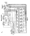
Figure 2 illustrates a more detailed block diagram of thestorage hub 10, in accordance with methods and systems provided. As illustrated, thestorage hub 10 includes a switch or switches 22-1 and 22-2, amanagement complex 26, and memory sections 30-1 through 30-n. In this embodiment, both switches 22-1 and 22-2 may be active or one of the switches may be active while the other is a redundant switch for use in the event the active switch suffers a problem. AlthoughFigure 2 illustrates two switches, thestorage hub 12 may include only one switch or any number of switches. - In
Figure 2 , server 12-2 connects to thestorage hub 10 via anetwork 20 through an input/output (I/0)controller 24. The network may be any type of internal or external network, such as an Ethernet network or the Internet. The I/O controller 24 preferably is an appropriate I/O controller for connecting to theparticular network 20. Preferably, the I/O controller 24 converts signals between a native protocol of thenetwork 20 and a local protocol used by thestorage hub 10. Potential protocols include, but are not limited to, Telecommunications Control Protocol/Internet Protocol (TCP/IP), System Network Architecture (SNA)-based protocols, Serial Communications Control Interface (SCCI), Intelligent Serial Communications Interface (ISCI), Fibre Channel, Infiniband, and other third generation input/output (3GIO) protocols - The
memory sections 30 preferably include the storage for thestorage hub 10 along with other hardware for accessing the storage. As used herein, the term "memory section" refers to any subsystem including one or more memory devices that may be used for storing information. This architecture is applicable to any device that can store data. Thus, when thestorage hub 10 receives a request to store data, the data is forwarded to amemory section 30, which stores the data. Likewise, when a request for data is received by thestorage hub 10, the request is directed to thememory section 30 storing the requested information. Thememory section 30 then reads the requested data, after which it is sent to theserver 12 requesting the data. More detailed descriptions ofexemplary memory sections 30 and their operations are presented below. - The
management complex 26 of thestorage hub 10 performs management-type functions for thestorage hub 10 and connects thestorage hub 10 with theexternal management system 14. As used herein the term "management complex" refers to any software and/or hardware for performing management of thestorage hub 10. A more detailed description of themanagement complex 26 is presented below. - The I/
O Controller 24 and switches 22-1 and 22-2 are preferably under common management control by themanagement complex 26 to allow data blocks to be sent to and received from the storage hub in the native protocol of thenetwork 20. - Each server 12-1 and 12-2 preferably includes a device driver 28-1 and 28-2, respectively. The
device driver 28 is a program running in software on a server that permits applications on the server to cause data to be read from or written to (i.e., stored in) thestorage hub 10. When aserver 12 receives a request to read or write data, thedevice driver 28 of theserver 12 forwards the request to the switch in thestorage hub 10. Thedevice driver 28 may be, for example, a standard device driver supplied as part of server-resident software, or it may be, for example, proprietary software supplied by a vendor of storage devices. Additionally, in some applications, thedevice driver 28 may be independent of any application resident on the server. - The switches 22-1 and 22-2 are connected to the server 12-1, the I/
O controller 24, theCDA 16, the memory sections 30-1 through 30-n, and each other via an industry standard communications interface protocol. These communications interface protocols may be, for example, Fibre Channel, Asynchronous Transfer Mode (ATM), Ethernet, Fiber Distributed Data Interface (FDDI) a Systems Network Architecture (SNA) interface, or X.25. Any type of physical connection, e.g., copper or fiber optic cables, may be used for connecting these various components. Themanagement complex 26 is preferably connected to theswitches 22, memory sections 30-l through 30-n, the I/O controller 26, and theexternal management system 14 via gigabit Ethernet connections. Although these are preferable connections, persons skilled in the art will recognize there are numerous other protocols and physical media that may be used to connect these devices. Further, thememory sections 30 may simultaneously support multiple protocols and physical media for connecting these devices. - The
switches 22 may be any type of switch using any type of switch fabric, such as, for example, a time division multiplexed fabric or a space division multiplexed fabric. As used herein, the term "switch fabric" the physical interconnection architecture that directs data from an incoming interface to an outgoing interface. For example, theswitches 22 may be a Fibre Channel switch, an ATM switch, a switched fast Ethernet switch, a switched FDDI switch, or any other type of switch. Theswitches 22 may also include a controller (not shown) for controlling the switch. - For write operations, the data block, in addition to being written to the
memory sections 30 of thestorage hub 10, may also be written to the cacheddisk array 16 or another storage hub (not shown). After the data is written, thestorage hub 10 may send an acknowledgement to thedevice driver 28 of theserver 12 depending upon the configuration management parameters in themanagement complex 26. Examples of configuration management parameters are status parameters, write-acknowledgement parameters, routing parameters, reporting interval parameters, and the current date and time. - For a read data block request and at the request of the
device driver 28 requesting the data block, theswitches 22 direct the request to theappropriate memory section 30, which retrieves the data block and transmits it through aswitch 22 to thedevice driver 28 of theserver 12 from which the request originated. - During read and write data block operations and depending on the configuration management parameters in the
management complex 26, thememory section 30 gathers administrative data that it sends to themanagement complex 26. Themanagement complex 26 then makes this data available to theexternal management system 14. - Additionally, the
management complex 26 may gather and provide theexternal management system 14 with surveillance and administrative information. Surveillance information may include, for example, memory section heartbeats (i.e., a signal that shows that the memory section can still communicate), alarms, and acknowledgement of alarms. Administration information may include, for example, statistics about data read and written, statistics about the number of active memory sections, statistics about memory section availability, and reports that present the preceding information to the external management system. - The
external management system 14 may also provide themanagement complex 26 with configuration management data. This configuration management information may include, for example, valid communications network addresses, a period for heartbeat intervals, data block sizes, and command sets. - The
storage hub 10 may also perform bit-level error recovery using standard means available in the industry. For example, error correction codes (ECC), also referred to as error detection and correction (EDAC) codes, using circuitry and/or software may be used to test data for its accuracy. These codes and techniques include parity bit or cyclic redundancy checks, using multiple parity bits in order to detect and correct errors, or more advanced techniques (e.g., Reed-Solomon codes) to detect multiple errors. Further, eachmemory section 30 of thestorage hub 10 may include its own error correction scheme. - The following provides a more detailed description of the components of the
storage hub 10 illustrated inFigure 2 : themanagement complex 26, theswitches 22, and thememory sections 30. After which, more detailed descriptions of exemplary reading, writing, and testing operations are presented. Then, alternative exemplary embodiments of thememory sections 30 are provided along with exemplary characteristics of thestorage hub 10 and its components. -
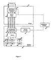
Figure 3 illustrates a logical architecture for amanagement complex 26, in accordance with methods and systems provided. As illustrated, themanagement complex 26 may include functions that manageadministrative processes 32 and functions that manage control processes 34. These management functions can include one or more central processing units (CPUs) for executing their respective processes. Additionally, themanagement complex 26 may use one or more application program interfaces (APIs) for communications between these functions. -
Figure 4 is a block diagram of a physical architecture for amanagement complex 26, in accordance with methods and systems provided. As illustrated, the management complex includes one or more control processors 34-1 through 34-n, a sharedmemory 36, one or more administration processors 32-1 through 32-m, astorage device 38, and acommunications network 40. As discussed above, thecontrol processors 34 may include one or more central processing units (CPUs). These control CPUs 34-1 through 34-n interface with the sharedmemory 36. Thecommunications network 40 may be an internal network and may use any type of communications protocol, such as Gigabit Ethernet. - One or more of the control processor (e.g., 34-1 through 34-m) may function as the master(s), while remaining control processors (e.g., 34-(m+1) through 34-n) may be kept in a hot standby mode, so that they can be quickly switched to in the event one of the master control processor (e.g., 34-1) fail.
- The control CPU's 34 may be attached to a communications network, such as a Gigabit Ethernet network, and be directly attached to the
magnetic storage device 38. - The
administrative processors 32 each may include a memory (not shown) and also be attached to thecommunications network 40. These administration processors may also connect to themagnetic storage device 38. Themagnetic storage device 38 stores various control and administrative information from thecontrol processors 34 andadministration processors 32. Themagnetic storage device 38 may be any type of magnetic storage device, such as, for example, servo-mechanical disc drives. In other embodiments, thestorage device 38 need not be included. - The
control processors 34 perform configuration management functions for thememory sections 30, I/O controllers 24, switches 22, and thedevice drivers 28 of theservers 12. As used herein, the term "configuration" is a broad term that encompasses the various possible operating states of each component of the storage hub. As used herein, an "operating state" refers to a possible way in which the storage hub or one of its components operates as defined by parameter values. These parameter values, for example, may be set by a user of the storage hub, such as, for example, a system administrator, through, for example, anexternal management system 14. Operating states may include, for example, how often a component (e.g., a memory section 30) sends performance statistics to themanagement complex 26, the list of events that causes a component (e.g., a memory section, etc.) to report an alarm, and/or the type of alarm reported (e.g., catastrophic failure of component, minor fault with component, etc.). Further, as used herein, the term "configuration management" means the understanding of the current operating states of the storage hub's components and the capability to react to changes in the states of those components as defined by software running in thecontrol processors 34. For example, thecontrol processors 34 may control in real time the number ofactive memory sections 30 in thestorage hub 10, theswitches 22, and thedevice drivers 28 of theservers 12, if any, and anyexternal servers 22 connected to the storage hub. - The software in the
control processors 34 may also be capable of bringing new memory sections into service and taking memory sections out of service independently of other functions that the management complex performs and without materially affecting the operation ofother memory sections 30 or adversely affecting the overall performance of the storage hub. The instructions to perform this function are carried from thecontrol process 34 to theswitches 22 and may be carried to thedevice drivers 28 in theservers 12. In the case that new capacity is added to thestorage hub 10, then it is possible to bringnew memory sections 30 into service with the software capability in thecontrol processors 32. In the case that amemory section 30 has failed, then thefaulty memory section 30 may be replaced and a new one brought into service. A further description of fault management follows. - The
control processors 34 may also, for example, be able to perform fault management for thestorage hub 10. The term "fault management" as used herein means attempting to detect faults and take corrective action in response to the detection of a fault. For example, the control processors may recognize an operational failure of amemory section 30 or part of amemory section 30 and re-map data to workingmemory sections 30. Then, thecontrol processors 34 may communicate this remapping to theexternal management system 14 and thedevice drivers 28 running onservers 12 attached to thestorage hub 10. - The
control processors 34 may also manage "bad-block" remapping functions when a memory section fails 30 and the writing of data to themagnetic storage device 38 in the event of power failures. Bad block remapping is a process wherein data blocks discovered by thesection controller 54 ormanagement complex 26 to be in a damaged memory device are, if possible, recovered. - For example, if the
control processors 34 discover that block 65,000 in memory section 30-2 does not read correctly, thecontrol processor 34 may decide to remap block 65,000 in memory section 30-2 to block location 1,999,998 in memory section 30-2. Thecontrol processor 34 may then direct theCDA 16 to read the data block and cause it to be written in location 1,999,998 in memory section 30-2. Once completed, thecontrol processor 34 may inform theswitches 22 and memory section 30-2 that block 65,000 may now be read from location 1,999,998. - As another example of bad block remapping, if for example only one memory device on a memory section is faulty, a
control processor 34 in themanagement complex 26 may inform thesection controller 54 about the bad device, determine where the data on the faulty memory device is backed-up (e.g., CDA 16), and direct the backed-up data to be loaded into a replacement memory device on the same memory section or on a different memory section. In the latter case, the management complex also informs the switch about the data being relocated to a new memory section. - As yet another example, in the event the
control processors 34 determine that amemory section 30 is faulty, thecontrol processors 34 may direct that theentire memory section 30 is taken out of service and that a replacement memory section takes its place. To accomplish this, thecontrol processors 34 may, for example, direct theCDA 16 to transfer a back-up version of the data for thefaulty memory section 30 to another memory section 30-N that may be, for example, aspare memory section 30 for use in the event amemory section 30 goes bad. The new memory section 30-N then may operate as though it were the nowfaulty memory section 30. Thecontrol processors 34 may then communicate this information to thevarious device drivers 28 and theexternal management system 14. - The
control processors 34 may also provide thememory sections 30, the switch controller(s) 202, and the I/O Controllers 24 with updated and new software. For example, if software used by thememory sections 30 or theswitches 22 become corrupted and/or fails, thecontrol processors 34 can load backup copies of current or previous versions of a software image from itsstorage 38. A software image is a binary object code that may be run directly by a computer. The software image for thecontrol processor 34 in one embodiment is stored on themagnetic storage 38. Further, thecontrol processors 34 may also control the loading of a data block from theCDA 16 into thememory sections 30 and visa versa. - In addition, the
control processors 34 may receive information such as, for example, the time a component sent an alarm or the total elapsed time a component was in alarm from the components of thestorage hub 10 over a communications interface. - The
control processors 34 also may allow theadministration processors 32 to gather data on parameters like the number ofactive memory sections 30, the total throughput of thestorage hub 10 over time, the size of memory section queues, etc., that comprise the operating state of the storage hub. (Note that memory section queues are those queues in the section controller that comprise the list of yet-to-be completed read operations and write operations). In addition, thecontrol processors 34 are responsible for monitoring their own operational status, such as, for example determining which control processor is active as Master, which are on standby, and which, if any, are not operational. Additionally, thecontrol processors 34 may monitor the Storage Hub's environment for extreme temperatures or humidity, etc. - The
control processors 34 may also store a copy of the software (i.e., a software image) run by theswitches 22. A more thorough description of theswitches 22 is present below. If the need arises, it can reload the switch software to one or more of the switches. As discussed below, theswitch 22 may include one or more switch controllers (not shown) for executing this software to control theswitch 22. In the event theswitch 22 uses multiple controllers configured in a master-slave architecture, thecontrol processor 34 may determine which of the controllers in the switch is(are) the master(s) and which is(are) the slave(s). - Additionally, the
control processors 34 may determine the status (active, idle, out-of-service) of ports (not shown) on theswitch 22, whether the ports are used to connect toservers 12 or tomemory sections 30. Thecontrol processors 34 may also provide configuration management data to theswitches 22. Examples of configuration management data include the date, the time, a routing algorithm to use, an interval for a status check, the identity of active server ports, etc. Further, thecontrol processors 34 may instruct the switch to use different "hunt" algorithms to find idle ports that may be used in establishing connections. These algorithms may be included in the software executed by the switch controller, examples of which include rotary hunt, skip route, and least-used. - The
administration processors 32 preferably collect information and statistics from the I/O controllers 24,memory sections 30, switches 22, and thecontrol processors 34. The information and statistics collected may include information for generating statistical reports, telemetry data, and other alarms and administrative data. Theadministration processors 32 provide this information to theexternal management system 14 using a protocol, such as, for example, TCP/IP or any other suitable protocol. Theadministration processors 32 may collect data on such parameters from thedevice drivers 28, theswitches 22, and thememory sections 30. - Users of the external management system, such as for example, a system administrator, may request a change in the configuration management parameters of the
storage system 10. This change may, for example represent the addition ofnew memory sections 30. Users of theexternal management system 14, such as for example, a system administrator, may also request theadministration processors 36 to collect statistical data from a storage area network environment (a set of storage devices connected by a network dedicated solely to the storage devices) including one ormore storage hubs 10, a network area storage environment (a set of storage devices connected by a network shared with other traffic) including one ormore storage hubs 10, and other external systems. For example, this statistical data may include the total incoming requests from each storage environment or from a particular server. - The
administration processors 32 may execute a database program such that the administration data is stored in a standard database, which can then be used to provide the information to system administrators of thestorage hub 10 in reports and graphs on a computer screen or on paper. For example, the system administrators of the storage hub may use anexternal management system 14 to gain access to this information. Alternatively, the system administrators of thestorage hub 10 may access this information directly through an interface to the administration processors. Like thecontrol processors 34, theadministration processors 36 can monitor themselves and communicate their own operational state to thecontrol processor 34, which determines whichadministration processors 34 are active or inactive for any reason. - The
management complex 26 may instruct a non-volatile storage device to load data into one or more of thememory sections 30. For example, as illustrated inFigure 2 , thestorage hub 10 may be connected to a non-volatile storage device such as aCDA 16. Themanagement complex 26 may then be able to send instructions to theCDA 16, switches 22, andmemory sections 30 to perform various activities. These activities may include the loading of thememory sections 30 from thenon-volatile storage device 16 when thestorage hub 10 is powered, when thestorage hub 10 has been restarted after, for example, having lost power in an outage, as a result of administrative changes to the configuration of thestorage hub 10, as a result of the failure of amemory section 30, or as a result of a user-initiated command. - Although the above presents numerous management and control functions capable of being performed by the
management complex 26, it should be understood that themanagement complex 26 may perform all, a subset, or even entirely different functions. Additionally, althoughFigures 3 and 4 illustrate an exemplary management complex being implemented usingseparate administration processors 32 andcontrol processors 34, a management complex may be implemented using only one, none, or any number of processors. -
Figure 5 is a block diagram of anexemplary memory section 30, in accordance with methods and systems provided. As illustrated, thememory section 30 may include a switch portal ("S-portal") 42, asection controller 54, a read only memory (ROM) 56, atemporary storage 58, a temporarystorage interface device 60, a temporary store selector ("T-selector") 62, asynchronizer 68, one or more memory interface devices 64-1 through 64-8, and one or more memory devices 66-1 to 66-n. - The
memory devices 66 may be any type of memory devices, such as, for example, dynamic random access memory (DRAMs), synchronous dynamic random access memory (SDRAMs), Rambus DRAMs (RDRAMs), magnetic random access memory, resistance random access memory, ferroelectric random access memory, polymer random access memory, chalcogenide random access memory, single in-line memory module (SIMMs), dual in-line memory module (DIMMs), rambus in-line memory modules (RIMMs), rotating media, etc. Although, the term memory interface device is used herein, it should be understood that this term should be interpreted broadly to include any type of access device capable of accessing information stored in a memory device. A more detailed description of exemplary memory interface devices is presented below. - The
section controller 54 may, for example, include a microprocessor 51,internal memory 52, a management complex interface(s) 53, memory device control circuitry 55, communications channel interface (CCI) control circuitry 57,test circuitry 59,timing circuitry 61, and a Header/test interface 63. The microprocessor 51 may be, for example, a chip such as the Motorola G2 executing appropriate software. Theinternal memory 52 may be, for example, 32 megabytes of useable SRAM for program and data storage. Thisinternal memory 52 may be included in the microprocessor 51, such as for example in a Motorola G2. Themanagement complex interface 53 may, for example, be a TCP/IP running over gigabit Ethernet interface that thesection controller 54 may use in communicating with themanagement complex 26. The header/test interface 63 may be an appropriate interface for providing information from thesection controller 54 to thememory interface devices 64. - The
section controller 54 further may access bootstrap read onlymemory 56 that may be used by it when power is first applied. This bootstrap read onlymemory 56 may, for example, contain a small software image that allows thesection controller 54 to communicate with thecontrol processors 34 to obtain the current software image via themanagement interface 53. Thesection controller 54 may further include CCI control circuitry 57 that may, for example contain a direct memory address circuitry for use in the management of thecommunications channel interface 46. - The
section controller 54 may also include memory device control circuitry 55 for controlling thememory devices 66. This memory device control circuitry 55 may, for example include a memory latching circuit for controlling the state of thememory devices 66 through the binary states of the memory latch. A further description of memory latching is presented below. Thesection controller 54 may further includetest circuitry 59 for testing thememory section 30. A more detailed description of an exemplary test procedure is presented below. Additionally, the section controller may include a header/test interface 63 for providing header type information (e.g., a data block identifier, destination address, etc.) and testing thememory section 30. Also, thesection controller 54 may include timingcircuitry 61 that may provide master and slave clock signal and other timing signals, such as start and stop read or write signals, etc. for use by the memory section. - The S-portal 42 may include a
selector 44 and acommunications channel interface 46. Thecommunications channel interface 46 provides the interface for connecting thememory section 30 with the one ormore servers 12 via theswitches 22. This connection may be, for example, via one or more fiber optic or copper cables. Theselector 44 may include circuitry for connecting thecommunications channel interface 46 with the one or morememory interface devices 64, such that theselector 44 may connect anymemory interface device 64 with any I/O port of thecommunications channel interface 46. Thesection controller 54 via the CCl circuitry 57 may provide control signals to theselector 44 regarding how the selector should connect thememory interface devices 64 andcommunication channel interface 46. Additionally, theselector 44 may be directed to send data, such as, for example, test data, from amemory interface device 64 to thesection controller 54 via the CCI circuitry 57. - The
communications channel interface 46 can use any type of protocol, such as, for example, any standard channel interface protocol and theselector 44 may or may not be included. Exemplary standard channel interface protocols include Fibre Channel, System Network Architecture-based protocols, Intelligent Serial communications Control Interface, and other third generation input/output (3GIO) protocols. - The temporary
storage interface device 60 is any type of device capable of accessing thetemporary storage device 58. For example, the temporarystorage interface device 60 may include one or more shift register arrays (not shown), including a plurality of shift registers interconnected in series, such that the data may be serially clocked through the shift register arrays. For a further description of shift register arrays and their use in accessing storage media such as memory devices, see the patent application by William T. Lynch and David J. Herbison, entitled "Methods and Apparatus for Improved Memory Access",US patent application 10/284, 198US patent 6879526 . - The
temporary storage 58 may be any type of memory device, such as a DRAM, SDRAM, SIMM, DIMM, a disk drive etc. The T-selector 62 may be any type of selector for selecting between a plurality of inputs. - The
storage hub 10 may use asynchronizer 68 in embodiments where the temporarystorage interface device 60 includes shift register arrays. In such an embodiment, thesynchronizer 68 may, for example, accept data to be stored in thememory section 30 and use phase lock loop circuitry to extract a clock frequency from the incoming data stream. A temporarystorage interface device 60 including shift register arrays may then use this clock signal to shift the data in writing data to thetemporary storage device 58. This clock signal may be used, for example, to compensate for possible differences in either the phase or frequency of the incoming data from the memory section's system clock. When data is shifted out of the temporarystorage interface device 60 for storage in thememory devices 66, the system clock for the memory section is preferably used to shift the data. - The
section controller 54 may be capable of detecting faults in thememory section 30. For example, thesection controller 54 may detect errors in the hardware or protocol used by the communications channel interface 42 through the communications channel interface circuit 57. Additionally, thesection controller 54 may, for example, detect errors in thememory interface device 64 through the use of the Header/Test interface 63. Further, if thememory devices 66 include circuitry for detecting and/or correcting faults, such as, for example, electronic error correction circuitry (e.g, DIMMs), thememory devices 66 may communicate detected faults to thesection controller 54 through the memory control 55. In the event thesection controller 54 detects a fault, thesection controller 54 may transmit information regarding the fault (e.g., time, component, type of fault) through themanagement interface 53 to themanagement complex 26. - The
section controller 54 may also include an interface available for an external system (not shown) that permits the external system to obtain information about thesection controller 54 through interaction with the microprocessor 51. This interface may, for example support a keyboard and display for direct diagnostic observations. The external system interface (not shown) may also, for example support an interface to a personal computer or similar system for direct diagnostic observations. The external system, not shown, may also use this interface, for example, to install special software on the microprocessor 51 in support of testing or related diagnostic functions. - The above description provides one example of an exemplary memory section. Other methods and systems may be used for implementing a memory section without departing from the scope of the invention. For example, the discussion below presents a different exemplary embodiment of a memory section using PCI bus technology.
-
Figure 6 illustrates a functional diagram of aswitch 22, in accordance with methods and system consistent with the invention. As illustrated, theswitch 22 includes a switch/server communications interface 204 for interfacing with aserver 12, a switch/memorysection communications interface 208, aswitch fabric 206, and aswitch controller 202. The switch/server communications interface 204 and switch/memorysection communications interface 208 may be standard switch interfaces found in commercially available switches and the terms memory section and server are used to indicate the devices to which the connections leaving theswitch 22 preferably connect. Theswitch fabric 22 may be any type of switch fabric, such as an IP switch fabric, an FDDI switch fabric, an ATM switch fabric, an Ethernet switch fabric, an OC-x type switch fabric, or a Fibre channel switch fabric. Thus, theswitch 22 may be any type of commercially available switch. - In this embodiment, the
management complex 26 of thestorage hub 10 may exercise control over theswitch 22 through theswitch controller 202, and may exercise control over thecommunications channel interface 46 of thememory section 30 through the section controller. For example, as discussed above, themanagement complex 26 may provide theswitch controller 202 with an algorithm for switching traffic through theswitch fabric 206. Further, as discussed above, themanagement complex 26 may provide other information including, for example, providing the switch with new copies of the software it executes, a regular period to send a heartbeat (i.e., a signal that verifies the switch still can communicate), a list of valid communications network addresses, alarm acknowledgements, and command sets. Further, as discussed above, themanagement complex 26 may provide other information including, for example, instructions to copy a communications message, modify its contents, and then process the new message. Themanagement complex 26 may provide other information including, for example, instructions to broadcast information to multiple addresses. -
Figure 7 illustrates an alternative functional diagram of the management of theswitch 22 and thecommunications channel interface 46 of thememory section 30, in accordance with methods and systems provided. In this embodiment, theswitch controller 202 and memory section interfaces 208 need not be included in theswitch 22, and themanagement complex 26 of thestorage hub 10 exercises direct control over theswitch fabric 206 and server interfaces 204. Thus, in this embodiment thecommunications channel interface 46 of thememory section 30 directly connects to theswitch fabric 206. - In an alternative embodiment to that of
Figure 6 and7 , theselector 44 need not be included and allmemory interface devices 64 may be connected to theswitch fabric 206. -
Figure 8 illustrates a diagram of an alternativeexemplary switch 22 that may be used in thestorage hub 10, in accordance with methods and systems provided. More particularlyFigure 8 illustrates aswitch 22 for connecting one ormore memory sections 30 to one ormore servers 12. This example illustrates M servers 12-1,12-2,... 12-M connected to asingle memory section 30. In this example, the server interfaces 204 of theswitch 22 include M switch/server communications interfaces (SSCI) 204-1 through 204-M, and the memory section interfaces 208 of the switch include N switch/memory section communications interfaces (SMCI) 208. Additionally, theswitch fabric 206 of theswitch 22 includes one or more switching planes 808. - In this example, the
servers 12 each includes adevice driver 28, and thememory section 30 includes one or more communications channel interfaces (CCI) 46-1 through 46-N. In this example, P parallel lines connect eachdevice driver 28 to theswitch 22 and eachCCI 46 to theswitch 22. Although in this example, the number of lines in each connection is equal, in other examples they may be different. Thedevice driver 28 may be, for example, the above-discusseddevice driver 28, or may be included in thedevice driver 28. - Any of the M servers may generate and transfer a data request from its
device driver 28 to amemory section 30 via theswitch 22. Aserver 12 may include in the data request a data block identifier that identifies a particular data block it wishes to write or a data block in thestorage hub 10 that it wishes to read. The correspondingSSCI 204 of theswitch 22 then receives the data request and forwards it to theswitch controller 202. Theswitch controller 202, in this example, determines thememory section 30 to which the information request is destined from the data block identifier included in the data request. - To determine the
memory section 30, theswitch controller 202 may, for example, consult a table that defines the relationship between data block identifiers and memory sections, use an algorithm to compute the address, or use some other technique. - Once the memory section is determined, the
switch controller 202 then may establish a transmission path through each switchingplane 808 for each of the parallel lines P from thedevice driver 28 to theSMCI 208 corresponding to thedetermined memory section 30. The data request may also be modified by theswitch controller 202 to contain a new address that may be used by theswitch 22 in directing the data request to thecorrect memory section 30. The modified data request is then transmitted across the switchingplanes 808 to theSMCI 208. This transmission across the P lines may be synchronous. - While the path through the switch is established, the data may reside in a separate storage queue (not shown) in the switch or in a memory (not shown) for the
switch controller 202. The data request may also be copied and further modified by theswitch controller 202 in accordance with any particular requirements of thestorage hub 10. For example, as previously discussed, themanagement complex 26 may instruct thestorage hub 10 to back up all data that is written to thestorage hub 10 or to one or moreparticular memory sections 30. In such an example, theswitch controller 202 may copy the write data request including the data to be stored and modify the request in accordance with any particular requirements of theCDA 16. Then, theswitch controller 202 may then establish a path for sending the write data request to theCDA 16 and then send the modified copy of the request to theCDA 16, so that the write data is backed up. Likewise, subsequent data blocks that comprise the write request may also be sent to thememory device 30 are copied and sent to theCDA 16. Themanagement complex 26 may, for example, provide theswitch controller 202 with any required information and software needed by the switch to determine how to modify data requests, provide multiple destinations with copies of modified data requests, and provide multiple destinations with copies of data. - When a
memory section 30 sends information such as data blocks to aserver 12, the data blocks from thememory section 30 arrive at theswitch 22 through theSMCI 208 corresponding to theCCl 46 for thememory section 30 sending the data block. The data blocks may include an identifier that is inserted into the data by thememory section 30. The memory interface devices of amemory section 30, for example, may insert this address, as described below. Further, this address may be for example a data block identifier identifying the particular data block that was read from thememory section 30, or a port or device to which the data is to be sent. In this example, P parallel lines connect eachCCI 46 to theswitch 22, although the number of lines in each connection may be different. Further, P may be any number greater than or equal to 1. - The
SMCI 208 then forwards the data block to theswitch controller 202, which determines theserver 12 to which the data block is destined from an identifier (e.g., data block identifier, destination address, etc.) within the transmitted data. Theswitch controller 202 then establishes with this destination address or data block identifier, for each of the P lines from theCCI 46, a path though theswitch 22 to theSSCI 204 to which the data is to be sent. Theswitch 22 then transfers the data block across the switchingplanes 808 to theSSCI 204. The transmission of a data block across the P lines may be, for example, synchronous. -
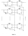
Figure 9 illustrates analternative switch 22 connected to one ormore memory sections 30, in accordance with methods and systems provided. In this example, muxing (the combining of several data streams into fewer data streams, each on its own communications path) and demuxing (the separation of a set of data streams into more data streams, each on its own communications path) are used in both thememory section 30 and theswitch 22. In this example, P parallel lines connect each memory section'sCCI 46 to theswitch 22, although the number of lines in each connection may be different. - In this example, in memory section 30-1, Q lines emanate from memory interface device 64-1 and R lines emanate from memory interface device 64-2. A corresponding mux (902-1 and 902-2) then multiplex the lines from each of these memory interface devices (64-1 and 64-2) into P streams, where, Q and R are positive integers greater than the positive integer P.
- In memory section 30-2, J lines emanate from memory interface device 64-4, where J is a positive integer less than P. A demux 904 then demuxes these J lines to P lines.
- The P parallel lines (streams), however, may also be muxed or demuxed anywhere along the switching path. For example, as illustrated, the P lines muxed into T-line by
mux 906 after the SMCI 208-1. The T-lines are then passed through the switchingplanes 808 todemux 908, which demuxes the T-lines into P lines and passes the P-lines to anSSCI 204. - Additionally, in embodiments employing a memory interface device including a shift array, one or more pipeline shift registers (not shown) may be inserted at points in the transmission and switching path to maintain the clock frequency of those transmissions at the appropriate multiple (muxing function) or sub-multiple (demuxing function) of the clock frequency of the memory interface device shift register array. For example, a shift register pipeline may be included in the
CCI 46. -
Figure 10 illustrates an exemplary pipeline shift register, in accordance with methods and systems provided. For this example, this pipeline shift register is inserted at the outputs of theCCI 46, such that each of the P lines exiting aCCI 46 are attached to a latch shift register 1002-1, 1002-2...1002-P. As illustrated, each of the P lines is attached to the S input of the latch shift register, and its inverse is connected to the R input of the latch shift register. The latch shift registers, further receive a master clock signal that may be generated by a master clock circuit for thestorage hub 10. This master clock signal may be used by other components in thestorage hub 10, such as, for example, the memory sections. The master clock signal may be, for example, generated by themanagement complex 26 or separate circuitry may be used. - The output, Q, from the latch shift register 1002 is then fed to the S input of a second latch register 1004, and the inverse of the output,
Q , is fed to the R input of the latch shift register 1004. The second latch shift registers 1004 receive a slave clock signal. This slave clock signal may be produced by the same circuitry providing the master clock signal, and the slave clock signal may be, for example, the inverse of the master clock signal. The outputs, Q, from these second latch shift registers 1004-1, 1004-2, ..., 1004-P then provide the signal to the P lines exiting thememory section 30. Although this description of a pipeline shift register was made with reference to latch shift registers, other types of shift registers may be used, such as, for example, dynamic shift registers. Further, although this description of a pipeline shift register was made with reference to attaching the pipeline shift registers to the outputs of theCCI 46, pipeline shift registers, may be included elsewhere in thestorage hub 10, such as, for example, at any communications interface or between the switching planes 808. -
Figure 11 includes a more detailed block diagram of an embodiment of amemory interface device 64, in accordance with methods and systems provided. As shown inFigure 11 , the memory interface devices 64-1 and 64-2 may each include a writeshift register array 72 and a read shift register array 74. Both the read and write shift register arrays can include a plurality ofshift registers 76 Interconnected in series. Eachshift register 76 of the shift register array (72 and 74) is connected to aconnector circuitry 77 which connects theshift register 76 to a corresponding I/O pin of thememory device 66. - As used herein, the term "shift register" refers to any register, device, stage or anything else with one or more selectable inputs that allows a signal to be received at an input and then output on the occurrence of some event, such as, for example, a control or clock signal. Although the term shift register sometimes refers to not just a single register stage, but also to a series of such registers, as used herein the term shift register refers to a single stage. A series of these shift registers is referred to herein as either a shift register chain, or a shift register string. The series set of registers is also sometime referred to as a "series array of (shift) registers" or shift register array that may be either a single chain of shift registers or parallel chains of shift registers. For example, the shift registers may be any type of shift register, whether dynamic or latching, whether single clock or master/slave clock, whether sampling or edge trigger, whether data (D), RS, or JK, or a stage of a charge coupled device (CCD), or any other type of device that shifts its input to an output on the basis of clock signal. The shift register arrays/chains may include any number of shift registers without departing from the scope of the invention.
- In this embodiment, all the write
shift register arrays 72 of thememory section 30 are interconnected to form a longer chain of write shift register arrays. As illustrated, theshift register array 72 of memory interface device 64-1 is connected via the top right I/O pin of memory interface device 64-2 to the writeshift register array 72 of memory interface device 64-2 via its top left I/O pin. The writeshift register array 72 of memory interface device 64-2 is then connected to the writeshift register array 72 of the memory interface device 64-3, and so on, such that all the writeshift register arrays 72 of the memory section form a single chain of write shift register arrays. For ease in explanation with regard to this particular example, the shift register arrays of each memory interface device will be referred to as a shift register array, and the interconnection of these shift register arrays to form a longer chain of arrays will be referred to as a shift register chain. - Further, in this embodiment, the bottom right I/O pin of memory interface device 64-1 connects to the bottom left I/O pin of memory interface device 64-2 such that their read shift register arrays 74 form a chain. Referring to
Figure 5 , note that in this example the memory interface devices 64-3 and 64-4 are likewise connected, and so on. These pairs of read shifter register arrays 74 will be referred to as read chains. - The first memory interface device in each read chain also includes a read selector 70 that is connected to the read shift register array 74. This read selector 70 is used for inserting an identifier (e.g., a destination address, data block identifier, etc.) and/or other header information into the read data. The identifier is an identifier that the
switches 22 preferably use to switch the data to its appropriate destination. The identifier may be, for example, an identifier for the data being transmitted (e.g., a data block identifier) or a destination address identifying an address to which to send the data. For example, if the destination is a computer connected to the internet, the destination address could be an IP address for the computer. Alternatively, the destination address could simply be an internal address for theswitches 22 to use in routing the data to its destination server, in which case theserver 12 will read and replace with a destination address that the network over which the data will travel uses to route the data to the appropriate destination. - The
memory interface device 64 may also receive control and timing signals from thetiming circuitry 61 of thesection controller 54. These control and timing pulses may be timed such that the data read from or written into amemory device 66 using the respective pulses are read or written in such a manner that the shift registers 76 of the memory interface device maintain their shifting as if only a shift was taking place. For a further description of memory interface devices incorporating shift registers, please see the aforementionedU.S. Patent Application Serial No. 10/284,198 by William T. Lynch and David J. Herbison , entitled "Methods and Apparatus for Improved Memory Access". Additionally, data transmitted by amemory interface device 64 may, for example, be transmitted in common mode, differential mode, or in any other manner as deemed appropriate by the system designers. -
Figure 12 illustrates a flow chart for an exemplary writing operation for thememory section 30 ofFigure 5 with reference toFigures 1 ,6 , and11 , in accordance with methods and systems provided. This flow chart illustrates but one example of a writing operation, and other methods may be used for implementing a write operation without departing from the scope of the invention. In this example, thememory devices 66 of thememory section 30 are partitioned into data blocks, where each data block is identifiable by a data block identifier. A more thorough description of data blocks and partitioning of memory devices are presented below. - A write request may originate, for example, from a user connected to a
server 12 via, for example, a network. In this example, it is assumed that the user sends a block of data (i.e., a data block) that is to be stored by thestorage hub 10. Adevice driver 28 in the server then may determine a data block identifier for the data block to be stored and send the request, including the data block identifier (DBI), to aswitch 22 within the storage hub 10 (Step 1202). Thedevice driver 28 may, for example, determine the data block identifier using standard methods, such as for example, theserver 12 may be executing Oracle or a similar type application, which may be used to determine the data block identifier. - The
switch 22 then may use the data block identifier (DBI) to direct the data request to thememory section 30 that is to store the data block by, for example, determining, based on the DBI, an address for the memory section that theswitch 22 uses to route the data request to the memory section (Step 1204). For example, when a data request arrives at anSSCI 204 of aswitch 22, the SSCI may, for example, direct the data request to theswitch controller 202, which may then, use a table to look up the address corresponding to the DBI, use an algorithm to compute the address from the DBI, or use some other method. - The
switch controller 202 may then establish a path through theswitch fabric 206 from theSSCI 204 to theSMCI 208 corresponding to the memory section where the data will be stored (Step 1206). If there is no idle communications channel between theswitch 22 and thememory section 30 or if there is a conflict, the switch may send a congestion message to the requestingserver 12, which may then queue the message until the conflict is resolved. In an embodiment of aswitch 22, such as that illustrated inFigure 7 , themanagement complex 26 may perform the functions described above as being performed by theswitch controller 202. - Next, the
switch 22 then forwards the data request to theCCI 46 of the memory section 30 (Step 1208); theCCI 46 then may direct the request to the section controller 54 (Step 1210). Thesection controller 54 identifies the data request as a write request, and determines if one of its memory devices has space to store the data (Step 1212). For example, thesection controller 54 may identify the request as a write request by information contained in the request itself, by the format or size of the data request, or by some other method. If there is noavailable memory device 66, thesection controller 54 sends a negative acknowledgement, NAK, message (Step 1214), through theCCI 46 and switch 22 to the requestingserver 12, which, after receiving the NAK (Step 1216), may attempt to rewrite the data to thestorage hub 10 using the same or a different DBI (Step 1218), may attempt to write to another device (not shown), or may inform the application. - If space is available, the
section controller 54 sends a message to thedevice driver 28 that it may transmit the data to be stored (Step 1220). In response, thedevice driver 28 transmits the data through theswitch 22 to the memory section's 30 communications interface (CCI) 46 (Step 1222). Additionally, themanagement complex 26 may also direct theswitch 22 to also send write data to theCDA 16. For example, themanagement complex 26 may provide an algorithm to theswitch controller 206 which when executed causes all write data to be sent to both thememory section 30 where the data will be stored and to theCDA 16. The version of the data stored by theCDA 16 will be treated as a back-up version that in the event the memory section suffers a fault may be loaded onto a different functioning memory section. - The
selector 44 then directs the data to the temporary storememory interface device 60. The microprocessor 51 of thesection controller 54 then checks the state of thememory device 66 where the data is to be stored to determine if thememory device 66 is available or is busy (Step 1224). For example, themicroprocessor 52 may store in its RAM 52 a status code for eachmemory device 66 in thememory section 30 that the microprocessor 51 may consult to determine the availability of thememory device 66. If thememory device 66 is available, the microprocessor 51 sends a message to thememory device 66 through the memory device control circuitry 55 to ready itself for storing the data (Step 1232). If, however, thememory device 66 is busy, the data temporary storagememory interface device 60 stores the data in the temporary memory storage device 58 (Step 1226) and a write request is placed in a queue in the microprocessor's RAM 52 (Step 1228). - When the
memory device 66 becomes available, thememory device 66 signals the microprocessor 51 in thesection controller 54 via the memory section control circuitry 55. (Step 1230). This may, for example, be accomplished by thememory device 66 sending an interrupt signal to the microprocessor 51 via the memory device control circuitry 55. Then, the microprocessor 51 sends a message to thememory device 66 through the memory device control circuitry 55 to ready itself for storing the data (Step 1232). When the memory device is ready, the temporary storagememory interface device 60 passes the data to the T-selector 62, which, because this is a write operation, passes the data to thememory interface device 60. For example, if thememory device 66 were available at Step 1222, the data need not be stored in the temporarymemory storage device 58. The data is then clocked into theshift register array 76 of the first memory interface device 64-1 where it is clocked through the write chain ofshift register arrays 76 until it is loaded into thememory interface device 64 corresponding to thememory device 66 to which the data is to be written (Step 1234). The data is then written to the memory device at an address supplied by thesection controller 54 of the memory section 30 (Step 1236). - A more detailed description of the connections between the shift register arrays and the memory devices and a method for writing the data is presented in the aforementioned
U.S. Patent Application Serial No.: 10/284,198 by William T. Lynch and David J. Herbison entitled "Methods and Apparatus for Improved Memory Access" filed on the same day as the present application. - When the write operation is complete, the
memory device 66 informs the microprocessor 51 in thesection controller 54 through the memory device interface 55 (Step 1238). Thesection controller 54 may then send an acknowledgement to thedevice driver 28 in the requesting server 12 (Step 1240). - The following provides a more detailed description of a technique that may be used in step 1236 for writing the data to the
memory device 66. This technique is referred to as memory latching. Memory latches may, for example be edge-triggered or flip flop circuits with common reset lines. That is, the memory device control circuitry 55 may, for example, include one or more of these memory latches along with other appropriate circuitry for performing this technique. - The
section controller 54 may reserve memory locations in itsinternal memory 52 for the management of thememory devices 66, which in this example are assumed to be DIMMs. These memory locations may be anywhere in theinternal memory 52 of thesection controller 54. - The memory device control circuitry 55 may read the data stored in these assigned memory locations, for example, by reading information being transmitted between the microprocessor 51 and the
memory 52 and looking at information addressed to these memory locations. These memory locations may store the starting address for data transfer, the number of binary digits to transfer, along with other control information for theDIMM 66. This control information may include, for example; information regarding whether the operation is a read or a write whether theDIMM 66 should start or terminate operations, etc. Although, the above describes one technique for writing data to a memory device in a memory section, one of skill in the art will recognize that numerous other methods are possible without departing from the scope of the invention. -
Figure 13 illustrates a flow chart for an exemplary reading operation for the memory section ofFigure 5 with reference toFigures 1 ,6 , and11 , in accordance with methods and systems provided. This flow chart illustrates but one example of a read operation and other methods may be used for implementing a read operation without departing from the scope of the invention. In this example, thememory devices 66 of thememory section 30 are partitioned into data blocks, where each data block is identifiable by a data block identifier. A more thorough description of data blocks and partitioning of memory devices is presented below. A read request may originate from a user connected to aserver 12 via a network. Adevice driver 28 in the server then sends the request, including a data block identifier (DBI), to aswitch 22 in the storage hub 10 (Step 1302). Thedevice driver 28 may, for example, determine the data block identifier using standard methods. For example, theserver 12 may be executing Oracle or a similar type application, which may be used to determine the data block identifier. - The
switch 22 then may use the data block identifier (DBI) to direct the data request to thememory section 30 that stores the data block, for example, by determining based on the DBI, an address for the memory section that the switch uses to route the data request to the memory section 30 (Step 1304). Theswitch controller 202 may then establish a path through theswitch fabric 206 from theSSCI 204 to theSMCI 208 corresponding to the memory section where the data will be stored (Step 1306). In the event there is no idle communications channel between theswitch 22 and thememory section 30 or there is a conflict, the switch may send a congestion message to the requestingserver 12, which may then queue the message until the conflict is resolved. In an embodiment of aswitch 22, such as that illustrated inFigure 7 , themanagement complex 26 may perform the functions described above as being performed by theswitch controller 202. Next, theswitch 22 then forwards the data request to theCCI 46 of the memory section 30 (Step 1308). TheCCI 46 then may direct the request to the section controller 54 (Step 1310). Thesection controller 54 identifies the data request as a read request, and determines if one of its memory devices stores the identified data block (Step 1312). For example, thesection controller 54 may identify the request as a read request by information contained in the request itself, by the format or size of the data request, or by some other method. - If the requested data block is not stored in the
memory section 30, thesection controller 54 sends a negative acknowledgement (NAK) message (Step 1314), through theCCI 46 and switch 22 to the requestingserver 12. After receiving the NAK (Step 1316), the requestingserver 12 may attempt to re-read (Step 1318) the data block from the memory section, may attempt to read the device from another device (not shown), or may inform the application. If thesection controller 54 verifies that the memory section stores the requested data block, the microprocessor 51 in thesection controller 54 determines whichmemory device 66 stores the data and checks its state to determine if thememory device 66 is busy or available (Step 1320). For example, as discussed above, themicroprocessor 52 may store in its internal memory 52 a status code for eachmemory device 66 in thememory section 30 that the microprocessor 51 may consult to determine the availability of thememory device 66. - If the memory device is available, the microprocessor 51 reserves the memory device by, for example, changing its state in the section controller's
internal memory 52 from available to busy. (Step 1326). Thesection controller 54 then may send an acknowledgement (ACK) (Step 1328), to the requestingserver 12. If thedevice driver 28 still wants to read the read the data block (Step 1330), it transmits a read confirmation through theswitch 22 to the memory section 30 (Step 1332). Otherwise, it abandons the read request (Step 1334). - Upon receipt of the read confirmation, the
section controller 54 provides an identifier to the read selector 70 of the first memory interface device 64-1 in the read chain corresponding to the memory device(s) 66 from which the data will be read (Step 1332). As discussed above, the identifier may be, for example, an identifier that theswitches 22 use to switch the data to its appropriate destination. The identifier may be, for example, an identifier for the data being transmitted (e.g., a data block identifier) or a destination address identifying an address to which to send the data. For example, if the destination is a computer connected to the Internet, the destination address could be an IP address for the computer. Alternatively, the destination address could simply be an internal address for theswitches 22 to use in routing the data to its destination server, in which case theserver 12 will read and replace with a destination address that the network over which the data will travel uses to route the data to the appropriate destination. - The identifier (e.g., destination address, a data block identifier, etc) is then clocked through the chain shift register arrays 74 of the
memory interface devices 64 until it reaches thememory interface device 64 corresponding to thememory device 66. That is, thememory device 66 that contains the data block corresponding to the data block identifier in the data request (Step 1336). Next, thesection controller 54 may then determine, using the data block identifier, the addresses for thememory device 66 corresponding to the storage locations where the data block to be read is stored. - The
section controller 54 then provides these addresses to thememory device 66 along with other appropriate control signals. In response, the memory device reads the data and it is loaded into the read shift register chain 74 of thememory interface device 64 such that the identifier (e.g., destination address, data block identifier, etc.) is appended to the front of the data (Step 1338). The addresses and control signals may be provided to thememory device 66 using a technique such as the above discussed memory latching technique. - If the
memory device 66 atstep 10 was busy, the read request may be queued in theinternal memory 52 of the microprocessor 51 (Step 1322). When the memory device becomes available, it may send an interrupt signal to the section controller 54 (Step 1324), which then executes the read request as described beginning at Step 1326. - When the data is clocked out of the shift register chain and sent to the selector 44 (Step 1340), the
selector 44, under the control of thesection controller 54, connects the data to the appropriate channel of thecommunications channel interface 46. The data is then passed to theserver 12 through thecommunications interface 208, theswitch fabric 206, and the communications interface 204 (Step 1342). - Additionally, data may be, for example, simultaneously read from all memory devices in a chain and simultaneously loaded into the read chain of shift register arrays. In such a situation, the identifier (e.g., destination address, data block identifier, etc.) may, for example, only be inserted at the front of the chain of shift register buses.
- A test operation for the embodiment of
Figure 5 will now be described. In certain instances, it may be desirable to test the system using known data. When testing the system, test data and a control signal are sent from thesection controller 54 to the T-selector 62 such that T-selector sends the test data to thememory interface devices 64 and the test data may be passed through the system. The test data after being written to and read from thememory interface devices 64 may then be sent to theselector 44, which may be, for example, instructed by thetest circuitry 59 to direct the test data to thetest circuitry 59. Thetest circuitry 59 may then check the data using error detection and correction capabilities, such as, for example, parity checks and/or bit level comparisons. If the data are correct, no action is required. If the data are not correct, the test data may be resent. If the data are then correct, no action is required. If not, thesection controller 54 may notify themanagement complex 26 that a fault has occurred and begin to isolate the fault through the error recovery capabilities present in the software it executes. In parallel, themanagement complex 26 may then execute fault management procedures, such as those discussed above in the section on themanagement complex 26. - Additionally, the CPU 51 may provide through the Header/
Test interface 63 test data to thememory interface devices 64. For example, this data may be sent to one or more of the shift register arrays of 64 in the same manner as destination addresses/data block identifiers and other data. Transmission of the data can be processed through thestorage hub 10 in the same manner as any formal data is processed and routed through thestorage hub 10. Such test data allows testing of the operations of all shift register arrays, all controls and interfaces, proper identification of server destinations, throughput time, checks on synchronism among the parallel data paths, etc. If desired, such a pathway may also be employed for any desired handshake routines prior to actual data delivery. - The
storage hub 10 may exhibit hierarchical parallelism. The phrase "hierarchical parallelism" as used herein refers to parallelism in the memory section, parallelism between the memory section and the switch fabric, and parallelism among all the memory sections through the switch fabric's connections to servers. - In this example, so long as the requested data are resident in
different memory devices 66, thememory section 30 itself may support N simultaneous reads and one write, where N is the number of communications channel connections available to thememory section 30 and preferably does not exceed the number ofmemory devices 66. For example, as illustrated inFigure 5 , thecommunications channel interface 46 has 4 communications channels connections for transmitting and receiving information. Theswitch 22 preferably can handle simultaneous read requests and write requests that it can fulfill. Thesection controller 54 of thememory section 30 preferably manages the reading and writing of data to thememory devices 66 and manages any conflicts. Thesection controller 54 of thememory section 30 manages conflicts through the capabilities present in the software it executes. For example, thesection controller 54 may direct that write requests have a priority than read requests with the lower priority requests being queued. For example, as previously discussed, the data for write requests may be queued in thetemporary storage device 58, and that write and read requests may be queued in theinternal memory 52 of thesection controller 54. Themanagement complex 26 may direct thesection controller 54 to resolve conflicts using other methods such as, for example, a first-to-arrive/a-first-to-be-processed algorithm. - I n this example, parallelism of the
memory sections 30 may be further augmented by parallelism amongmemory sections 30. That is, at any point in time and so long as the number ofmemory sections 30 is at least as great as the number of server connections, S, from thestorage hub 10, then as many as S memory sections may be accessed. In the event thestorage hub 10 has more server connections than memory sections, then, in this example, the number of simultaneous transactions equals the number of memory sections. - In addition, the
storage hub 10, in this example, may also be scalable. More particularly, if increased capacity is demanded from thestorage hub 10, this increased capacity may be handled by, for example, addingadditional memory sections 30 and cabinets to house them, including backup power, higher capacity and/oradditional switches 22, and/or increasing the number and/or capacity of the connections to thestorage hub 10. Additionally, as the capacity of thestorage hub 10 is increased, the capacity and/or number of management complex processors (32 and 34) may be increased, if necessary, to ensure that themanagement complex 26 has sufficient capacity to monitor the respective states of the storage hub'smemory sections 30 - Additionally, in this example, the
memory sections 30 may also be scalable. For example, increased capacity of amemory section 30 may be obtained by, for example, addingadditional memory devices 66,memory interface devices 64, and/or communications channel interfaces to the memory section. Preferably, thesection controller 54 for each memory section includes a sufficiently large resident memory for holding a "map" of the location of each data block resident in itsmemory section 30. Commercially available microprocessors may be used by the section controller for storing this map. - A scalable architecture may initially be deployed wherein the storage hub includes only one or a few memory sections each including only small number of memory devices. Then, as increased capacity is demanded of the storage hub, this increased capacity may be managed, for example, by adding additional and/or higher capacity memory sections to the storage hub additional cabinets and backup power to house the additional memory sections, increasing the capacity of the existing one or more memory sections, increasing the capacity of the
management complex 26 through the addition ofcontrol processors 34 oradministration processors 34, increasing the ' number and/or capacity of theswitches 22 through the addition of more ports and/or switch controllers as needed. Thus, as the storage hub's capacity is increased, the performance seen by any given user preferably remains uniform as the system grows, and expected response times for users with applications generating random data requests preferably remains uniform as the system expands. -
Figure 14 illustrates a logical diagram ofN memory devices 66, in accordance with methods and systems provided. As discussed above, thememory devices 66 may be solid state memory devices that can store B bits, and the number of bits that each memory device can store may be different. In one example, themanagement complex 26 may send a command to thesection controller 54 of amemory section 30, instructing thesection controller 54 to reconfigure amemory device 66 in thememory section 30 into a number of partitions including one or more data blocks each having a particular block size, where the block size is the number of bits in the block. Use of differently sized data blocks and data block partitions allows the storage hub to suit its storage structure to different applications whose data are stored on the same storage hub. For example, an application like an on-line catalog that always stored text and an image or images should preferably prefer a larger block size than an application like a customer reservation system that stored only text. Since the partitions and block sizes can be reconfigured at will through commands from the management complex, new data for new applications may be loaded into the storage hub without have to stop its operations or affect data in other memory sections that are not being changed. - As illustrated in
Figure 14 , memory device 66-1 has two partitions, where the first partition includes eight blocks and the second includes two blocks. In this example, the block size of the data block in the first partition is smaller than the data blocks in the second partition. Memory device 66-2, in contrast, has four identical partitions of four blocks each, where each data block is of equal size Additionally, in this example, themanagement complex 26 may dynamically adjust the data block size in each partition, modify the partitions, or add or delete partitions. For example, at any time themanagement complex 26 may instruct thesection controller 54 of amemory section 30 to reconfigure thememory devices 66, wherein the current partition may have no effect on any subsequent partition. -
Figure 15 illustrates an embodiment wherein the memory interface devices use a common shift register array for reading from and writing to the memory device, in accordance with methods and systems provided. As illustrated, eachmemory interface device 64 includes ashift register array 78 of a plurality ofshift registers 76 interconnected in series. Further, like the embodiment ofFigure 11 , these memory interface devices are connected in pairs to form a chain. - As illustrated, the
shift register array 78 of memory interface device 64-1 is connected to theshift register array 78 of memory interface device 64-2, which is in turn connected to theselector 44. Further, because there is not a separate write chain, the I/O pins in the upper right and left of thememory interface devices 64 shown inFigure 5 are not necessary. Additionally, the memory interface devices of this embodiment use awrite selector 82. The operation of thewrite selector 82 will be described in more detail below. - The following provides a description of exemplary write operation for the embodiment of
Figure 15 . Data to be written to thememory devices 66, as in the above embodiment ofFigure 11 is forwarded through the Temporarystorage interface device 60 to the T-sefector 62 under the control of thesection controller 54. In this embodiment, because there are separate chains for writing the data, the data is forwarded to the chain corresponding to thememory device 66 where the data is to be stored. The T-selector 62, therefore, passes the data to thewrite selector 82, which receives a control signal from thesection controller 54 such that thewrite selector 82 sends the data to the appropriate chain of shift register arrays. - The signal is then passed to the
read selector 76 of the first memory interface device 64-1 (in this example) in the chain. Because, this is a write operation, the data is clocked into theshift register array 78 and is clocked through the shift registers until it is loaded into theshift register array 78 corresponding to thememory device 66 to which the data is to be written. The data is then written to thememory device 66. Methods and systems for writing data from ashift register array 78 to amemory device 66 are presented in more detail below. - An exemplary reading operation for the embodiment of
Figure 15 will now be described. First, an identifier (e.g., destination address, data block identifier, etc.) for the data is supplied to theread selector 84 from thesection controller 54. The destination address is then clocked through the chain of shift register arrays. - Next, the data is loaded from the
memory device 66 into theshift register array 78 such that the identifier (e.g., destination address, data block identifier, etc.) is appended to the front of the shift register array. The data is then clocked through the chain ofshift registers 76 until it is passed to theselector 44. The data is then passed to the end user through theserver 12 as was described with reference toFigures 5 and11 . - Additionally, as in
Figure 11 , test data may be inserted into thememory devices 66 and passed through the system using the T-selector 62. - As will be obvious to one of skill in the art, other embodiments of the memory interface device are possible, without departing from the scope of the invention. For example, although each memory interface device is described as only having one read or write shift register array, the memory interface device may include any number of write or read chains of shift register arrays. Further, the shift registers 76 rather than being 1 bit shift registers may be of any depth. For example, the shift register arrays could be, for example, NxM arrays such as, for example, 2x8, 4x32, 8x16, etc. arrays as determined by the system designers for their particular implementation. Additionally, the shift registers arrays may be configured in a ring, such that the data once loaded into a chain circulates synchronously in the chain. A more detailed description of memory access using shift register arrays is set forth in the aforementioned
U.S. Patent Application Serial No. 10/284,198 by William T. Lynch and David J. Herbison entitled "Methods and Apparatus for Improved Memory Access" filed on the same day as the present application. -
Figure 16 illustrates analternative memory section 30, in accordance with methods and systems provided. These memory sections are provided as exemplary mechanisms that could be employed to practice the invention, and are not intended to limit the scope of the claims. - As illustrated, the
memory section 30 includes one or more communications channel input/output interfaces 46-1 and 46-m, asection controller 54, one or more bus interfaces 1602, abus 1604, abus controller 1606, ananalyzer 1608, and one or more memory devices 66-1 and 66-n. In this example, thebus 1604 uses the Peripheral Component Interconnect (PCI) standard. Each device is preferably connected to the bus via a bus interface 1602, which in this example is a PCI interface. Thebus controller 1606 in this example is a PCI bus controller for arbitrating which device may control the bus. Additionally, in this example, ananalyzer circuit 1608 monitors the state of thePCI bus 1604 and informs thesection controller 54 of the real time state of thebus 1604. - The communications channel input/output interfaces 46-1 and 46-m may be any type of communications channel interfaces, such as Fibre Channel, Telecommunications Control Protocol/Internetworking Protocol (TCP/IP) over Ethernet, Token Ring, etc.. In this example, the communications channel input/output interfaces 46-1 and 46-m use the Fibre Channel protocol. A commercially available Fibre Channel I/O component embodied on a chip may be used as the communications channel I/O interfaces 46. These commercially available chips typically include a microprocessor for executing
layer section controller 54 regarding control of the PCI interfaces 1602 and transferring or receiving information from thememory devices 66. In this example, m number communication channel I/O interfaces are illustrated, where m >= 1. - The communications channel I/O interfaces 46 preferably also are capable of receiving control instructions from the
section controller 54. For example, thesection controller 54 may send and receive control information to and from the communications channel interfaces 46 using the direct memory addressing (DMA) protocol. Additionally, although not shown, thesection controller 54 may also send and receive interrupts and I/O commands to and from the communication channel interfaces 46 over one or more I/O control lines. - In this example, the
section controller 54 is embodied on one or more chips including an internal random access memory, a read only memory for bootstrap loading, an interface to the Management Complex, and a microprocessor. Thesection controller 54 may directly control thememory devices 66 through memory latching, as in the above-described embodiment. Additionally, thesection controller 54 may receive real time status information about the bus interfaces 1602 from theanalyzer circuit 1608. Thesection controller 54, as illustrated, also includes a DMA interface for sending and receiving control information to/from the communications channel interfaces using the DMA protocol. Although, in this example, the DMA protocol is used, as discussed above any other suitable protocol may be used for sending control information between the communication channel interfaces 46 and thesection controller 54. - The read only memory (ROM) 56 may store the software associated with the bootstrap program used by the section controller to obtain its latest software image. This
ROM 56 although illustrated as separate from thesection controller 54 may be included in thesection controller 54. - The bus interfaces 1602 are used to connect the
memory devices 66 and communications channel interfaces 46 to thebus 1604, such that these devices may transmit and receive information over thebus 1604. The bus interfaces 1602-3 and 1602-4 in this example connect to thesection controller 54 via control lines over which thesection controller 54 may send to the bus interfaces 1602-3 and 1602-4 control information. This control information may include, for example, an identifier (e.g., destination address, data block identifier, etc.) for data being read from thememory device 10. Accordingly, the bus interfaces 1602-3 and 1602-4 may also be referred to as memory interface devices 1602-3 and 1602-4. - The
memory devices 66, as in the above-described embodiments may be any type of memory devices, such as, for example DIMMs. Thesection controller 54 preferably controls reading from and writing to thememory devices 66. For example, control lines between thememory devices 66 and thesection controller 54 may carry signals from thesection controller 54 to thememory devices 66 regarding the address to transfer data to/from, and the number of bits to transfer data to/from thememory device 66. Additionally, thememory devices 66 may be capable of providing thesection controller 54 via these control line with a real time interrupt signal when an operation is complete along with information regarding the operational status of thememory device 66. In this example, there aren memory devices 66, where n>=1. - The following provides a brief overview of an example for a reading operation for the memory section of
Figure 14 . In this example, the communications channel interfaces 46 are preferably fibre channel I/O components. When a data request arrives at thecommunications channel interface 46, thecommunication channel interface 46 detects it and sends an interrupt signal to thesection controller 54. This interrupt signal preferably includes information regarding the data block to be read from the memory devices. Thesection controller 54 then maps this data block information to an address in the memory devices. That is, the section controller determines from this data block information thememory devices 66 storing the requested data along with the addresses for this data on those memory devices. Thesection controller 54 then loads this address information into its internal memory, such that the addresses are transferred to the memory devices as in the above-describe memory latching example. - The requested data block is then read from the
memory devices 66 and transferred to their corresponding bus interfaces 1602. Additionally, thesection controller 54 transmits an identifier (e.g., destination address, data block identifier, etc.) to the bus interface 1602. The identifier may be, for example, an identifier for the data being transmitted (e.g., a data block identifier) or a destination address identifying an address to which to send the data. The destination address may be, for example, the internal address for the bus interface 1602 corresponding to thecommunication channel interface 46 to which the data is to be sent. Alternatively, the destination address may be, for example, an address of theserver 12 to which the data is destined, an address for use by theswitch 22 in switching the information, or any other identifier useful in routing the data towards its destination. - The bus interfaces 1602 then transfer the identifier (e.g., destination address, data block identifier, etc.) and the data over the
bus 1604 according to the bus's protocol. In this example, thebus 1604 uses the PCI protocol and thePCI controller 1606 arbitrates any conflicts in accessing thebus 1604. - The bus interface 1602 for the
communication channel interface 46 to which the data is sent monitors the bus for data including its address. Because all information is transmitted over the bus, bus interfaces 1602 ignore data not including an address for the bus interface 1602. When the bus interface 1602 for thecommunication channel interface 46 to which the data is to be transmitted recognizes an address for itself, it reads the data from thebus 1604. Thecommunication channel interface 46 then transmits the data block from thememory section 30. In certain examples, thecommunications channel interface 46 may also replace the destination address with a new destination address prior to sending the data from thememory section 30. - A write operation for the
exemplary memory section 30 ofFigure 14 will now be described. When a write request is received by acommunications channel interface 46, thecommunications channel interface 46 determines that it is a write request and forwards the request to thesection controller 54 via theDMA interface 1610. The write request in this example may include a data block identifier indicative of where thememory section 30 is to write the data. Thesection controller 54 then maps this data block identifier to determine thememory devices 66 to which thememory section 30 is to write the data along with the addresses for thememory devices 66. Thesection controller 54 provides these addresses to theappropriate memory devices 66. - In addition to sending the write data request to the
section controller 54, thecommunications channel interface 46 obtains the data from the write request and sends the data to the communication channel interface's corresponding bus interface 1602. Additionally, thesection controller 54 may supply thecommunications channel interface 46 with a bus interface address for the bus interface 1602 corresponding to thememory device 66 that will store the write data. The bus interface 1602 then transmits the data and the bus interface onto thebus 1604. - The bus interfaces 1602-3 and 1602-4 for the memory devices monitor the
bus 1604 looking for data destined for them. When the bus interface 1602 senses its address is being transmitted, it reads the write data from the bus. Meanwhile, thesection controller 54 informs thecorresponding memory device 66 to accept write data from its bus interface 1602-3 or 1602-4. The bus interfaces 1602-3 or 1602-4 then provide the data to theircorresponding memory device 66 which write the data at the address provided by thesection controller 54.
The above description of the preferred embodiments has been given by way of example. From the disclosure given, those skilled in the art shall understand the invention and its advantages, but will also find apparent various changes and modifications that can be made to the methods and structures disclosed. Thus, it is intended that the specification and examples be considered as exemplary only, with a true scope of the invention being indicated by the following claims.
Claims (8)
- A storage system, comprising:one or more memory sections (30), including
one or more memory devices (66) having storage locations for storing data, and a memory section controller (54) capable of detecting faults in the memory section (30) and transmitting a fault message in response to the detected faults; andone or more switches (22), includinga management system (26) capable of receiving fault messages from the memory section controllers (54) and removing from service the memory section from which the fault message was received by changing the routing algorithm, and wherein the management system (26) is adapted to determine the routing algorithm for use by the switch fabric (206) in interconnecting the memory sections (206) and the external device interfaces (204), provide the determined routing algorithm to the switch controller (202) and instruct the switch controller (202) to execute the determined routing algorithm.
one or more interfaces (204) for connecting to one or more external devices; and
a switch fabric (206) connected to one or more memory sections (30) and the external device interfaces (204) and interconnecting the memory sections (30) and the external device interfaces (204);
characterised in that said interconnecting of the memory sections (30) and the external device interfaces (204) is based on a routing algorithm executed by a switch controller (202) that executes software including the routing algorithm and by - The storage system of claim 1, wherein the management system (26) exercises direct control over the switch fabric and the external device interfaces.
- The storage system of claim 1 or claim 2, wherein the management system (26) is further capable of providing software images to the switch controller (202) and to the memory section controllers.
- The storage system of any preceding claim, wherein a plurality of parallel lines connect at least one of the memory sections (30) to a switch, and wherein data from the memory section is passed through the switch fabric (206) of the switch in parallel.
- The storage system of any preceding claim, wherein the management system (26) includes:one or more control processors (34) for determining and providing the algorithm to the switch; andone or more administration processors (32) for collecting statistical data from the one or more switches and the one or more memory sections.
- A method for use in a storage system, comprising:storing data in storage locations in a memory device (66), the memory device (66) included in a memory section (30); the method being characterised bya management system (26) determining a routing algorithm for use by a switch (22);execution by a switch controller (22) of software, including the routing algorithm, in connecting the memory section (30) and an external device interface (204);the management system (26) providing the determined routing algorithm to the switch controller (202), and instructing the switch controller (202) to execute the determined routing algorithm;the switch (22) connecting the memory section (30) to the external device interfaces (204) based on the routing algorithm;detecting by a memory section controller (54) of a fault in regard to the data stored in the memory device (66) and transmitting a fault message in response to the detected fault to the management system (26);receiving the fault message at the management system (26); andthe management system (26) removing from service the memory section (30) from which the fault message was received by changing the routing algorithm.
- The method of claim 6, further comprising:the management system (26) instructing a non-volatile storage device to load data into a memory section (30) via the switch (22); andstoring the data from the non-volatile storage device in a memory device in the memory section.
- The method of claim 6 or claim 7, wherein the storage locations of the memory devices (66) are partitioned into data blocks, the data blocks identifiable by a data block identifier, and wherein a data request received by the storage system includes a data block identifier, further comprising:the switch (22) directing the data request to a memory section including the memory device storing the data block identified by the data block identifier;the memory section reading from the memory device data stored in the storage locations of the memory devices identified by the data block identifier; andforwarding the read data to a destination device via the switch.
Priority Applications (2)
| Application Number | Priority Date | Filing Date | Title |
|---|---|---|---|
| EP09153548A EP2060976B1 (en) | 2002-10-31 | 2003-10-23 | Methods and systems for a storage system |
| EP10184634A EP2302517B1 (en) | 2002-10-31 | 2003-10-23 | Storage system and method for use in a storage system |
Applications Claiming Priority (7)
| Application Number | Priority Date | Filing Date | Title |
|---|---|---|---|
| US284268 | 1988-12-14 | ||
| US10/284,268 US7707351B2 (en) | 2002-10-31 | 2002-10-31 | Methods and systems for an identifier-based memory section |
| US284199 | 2002-10-31 | ||
| US10/284,199 US7197662B2 (en) | 2002-10-31 | 2002-10-31 | Methods and systems for a storage system |
| US10/284,278 US7415565B2 (en) | 2002-10-31 | 2002-10-31 | Methods and systems for a storage system with a program-controlled switch for routing data |
| US284278 | 2002-10-31 | ||
| PCT/US2003/033665 WO2004042505A2 (en) | 2002-10-31 | 2003-10-23 | Methods and systems for a storage system |
Related Child Applications (1)
| Application Number | Title | Priority Date | Filing Date |
|---|---|---|---|
| EP09153548A Division EP2060976B1 (en) | 2002-10-31 | 2003-10-23 | Methods and systems for a storage system |
Publications (3)
| Publication Number | Publication Date |
|---|---|
| EP1565819A2 EP1565819A2 (en) | 2005-08-24 |
| EP1565819A4 EP1565819A4 (en) | 2007-11-21 |
| EP1565819B1 true EP1565819B1 (en) | 2009-04-22 |
Family
ID=32314844
Family Applications (3)
| Application Number | Title | Priority Date | Filing Date |
|---|---|---|---|
| EP03777844A Expired - Lifetime EP1565819B1 (en) | 2002-10-31 | 2003-10-23 | Methods and systems for a storage system |
| EP10184634A Expired - Lifetime EP2302517B1 (en) | 2002-10-31 | 2003-10-23 | Storage system and method for use in a storage system |
| EP09153548A Expired - Lifetime EP2060976B1 (en) | 2002-10-31 | 2003-10-23 | Methods and systems for a storage system |
Family Applications After (2)
| Application Number | Title | Priority Date | Filing Date |
|---|---|---|---|
| EP10184634A Expired - Lifetime EP2302517B1 (en) | 2002-10-31 | 2003-10-23 | Storage system and method for use in a storage system |
| EP09153548A Expired - Lifetime EP2060976B1 (en) | 2002-10-31 | 2003-10-23 | Methods and systems for a storage system |
Country Status (7)
| Country | Link |
|---|---|
| EP (3) | EP1565819B1 (en) |
| JP (2) | JP2006505065A (en) |
| KR (3) | KR20100072068A (en) |
| AT (3) | ATE557349T1 (en) |
| AU (1) | AU2003286638A1 (en) |
| DE (2) | DE60335926D1 (en) |
| WO (1) | WO2004042505A2 (en) |
Cited By (1)
| Publication number | Priority date | Publication date | Assignee | Title |
|---|---|---|---|---|
| US7707351B2 (en) | 2002-10-31 | 2010-04-27 | Ring Technology Enterprises Of Texas, Llc | Methods and systems for an identifier-based memory section |
Families Citing this family (11)
| Publication number | Priority date | Publication date | Assignee | Title |
|---|---|---|---|---|
| US6879526B2 (en) | 2002-10-31 | 2005-04-12 | Ring Technology Enterprises Llc | Methods and apparatus for improved memory access |
| US7058738B2 (en) * | 2004-04-28 | 2006-06-06 | Microsoft Corporation | Configurable PCI express switch which allows multiple CPUs to be connected to multiple I/O devices |
| JP4819369B2 (en) * | 2005-02-15 | 2011-11-24 | 株式会社日立製作所 | Storage system |
| US8307180B2 (en) | 2008-02-28 | 2012-11-06 | Nokia Corporation | Extended utilization area for a memory device |
| US7941697B2 (en) | 2008-12-30 | 2011-05-10 | Symantec Operating Corporation | Failure handling using overlay objects on a file system using object based storage devices |
| US8874824B2 (en) | 2009-06-04 | 2014-10-28 | Memory Technologies, LLC | Apparatus and method to share host system RAM with mass storage memory RAM |
| US9417998B2 (en) | 2012-01-26 | 2016-08-16 | Memory Technologies Llc | Apparatus and method to provide cache move with non-volatile mass memory system |
| US9311226B2 (en) | 2012-04-20 | 2016-04-12 | Memory Technologies Llc | Managing operational state data of a memory module using host memory in association with state change |
| WO2015089488A1 (en) | 2013-12-12 | 2015-06-18 | Memory Technologies Llc | Channel optimized storage modules |
| US10255134B2 (en) * | 2017-01-20 | 2019-04-09 | Samsung Electronics Co., Ltd. | Control plane method and apparatus for providing erasure code protection across multiple storage devices |
| KR20230085629A (en) * | 2021-12-07 | 2023-06-14 | 에스케이하이닉스 주식회사 | Storage device and operating method thereof |
Family Cites Families (19)
| Publication number | Priority date | Publication date | Assignee | Title |
|---|---|---|---|---|
| US4914657A (en) * | 1987-04-15 | 1990-04-03 | Allied-Signal Inc. | Operations controller for a fault tolerant multiple node processing system |
| JPH0795258B2 (en) * | 1988-12-22 | 1995-10-11 | 富士通株式会社 | Redundant disk control method |
| US4984240A (en) * | 1988-12-22 | 1991-01-08 | Codex Corporation | Distributed switching architecture for communication module redundancy |
| US5134619A (en) * | 1990-04-06 | 1992-07-28 | Sf2 Corporation | Failure-tolerant mass storage system |
| JP2829091B2 (en) * | 1990-04-19 | 1998-11-25 | 株式会社東芝 | Data processing system |
| US5729763A (en) * | 1995-08-15 | 1998-03-17 | Emc Corporation | Data storage system |
| US5922077A (en) * | 1996-11-14 | 1999-07-13 | Data General Corporation | Fail-over switching system |
| JPH1117775A (en) * | 1997-06-20 | 1999-01-22 | Sony Corp | Serial interface circuit |
| JP2000242434A (en) * | 1998-12-22 | 2000-09-08 | Hitachi Ltd | Storage device system |
| US6370605B1 (en) * | 1999-03-04 | 2002-04-09 | Sun Microsystems, Inc. | Switch based scalable performance storage architecture |
| IE20000203A1 (en) * | 1999-03-25 | 2001-02-21 | Converge Net Technologies Inc | Storage domain management system |
| JP3454183B2 (en) * | 1999-04-13 | 2003-10-06 | 日本電気株式会社 | Disk array device |
| JP3726559B2 (en) * | 1999-06-01 | 2005-12-14 | 株式会社日立製作所 | Direct backup method and storage system |
| JP4175764B2 (en) * | 2000-05-18 | 2008-11-05 | 株式会社日立製作所 | Computer system |
| GB2367648B (en) * | 2000-10-03 | 2002-08-28 | Sun Microsystems Inc | Multiple trap avoidance mechanism |
| US8949471B2 (en) * | 2000-11-02 | 2015-02-03 | Oracle America, Inc. | TCP/UDP acceleration |
| US6880100B2 (en) * | 2001-07-18 | 2005-04-12 | Smartmatic Corp. | Peer-to-peer fault detection |
| US6947981B2 (en) * | 2002-03-26 | 2005-09-20 | Hewlett-Packard Development Company, L.P. | Flexible data replication mechanism |
| US6879526B2 (en) | 2002-10-31 | 2005-04-12 | Ring Technology Enterprises Llc | Methods and apparatus for improved memory access |
-
2003
- 2003-10-23 DE DE60335926T patent/DE60335926D1/en not_active Expired - Lifetime
- 2003-10-23 EP EP03777844A patent/EP1565819B1/en not_active Expired - Lifetime
- 2003-10-23 WO PCT/US2003/033665 patent/WO2004042505A2/en active Application Filing
- 2003-10-23 JP JP2004550085A patent/JP2006505065A/en active Pending
- 2003-10-23 AT AT10184634T patent/ATE557349T1/en active
- 2003-10-23 AT AT03777844T patent/ATE429676T1/en not_active IP Right Cessation
- 2003-10-23 AU AU2003286638A patent/AU2003286638A1/en not_active Abandoned
- 2003-10-23 AT AT09153548T patent/ATE497208T1/en not_active IP Right Cessation
- 2003-10-23 KR KR1020107009973A patent/KR20100072068A/en not_active Application Discontinuation
- 2003-10-23 DE DE60327357T patent/DE60327357D1/en not_active Expired - Lifetime
- 2003-10-23 EP EP10184634A patent/EP2302517B1/en not_active Expired - Lifetime
- 2003-10-23 KR KR1020107009972A patent/KR20100072067A/en not_active Application Discontinuation
- 2003-10-23 KR KR1020057007547A patent/KR20050075764A/en not_active Application Discontinuation
- 2003-10-23 EP EP09153548A patent/EP2060976B1/en not_active Expired - Lifetime
-
2010
- 2010-03-29 JP JP2010076275A patent/JP2010250813A/en active Pending
Cited By (2)
| Publication number | Priority date | Publication date | Assignee | Title |
|---|---|---|---|---|
| US7707351B2 (en) | 2002-10-31 | 2010-04-27 | Ring Technology Enterprises Of Texas, Llc | Methods and systems for an identifier-based memory section |
| US7941595B2 (en) | 2002-10-31 | 2011-05-10 | Ring Technology Enterprises Of Texas, Llc | Methods and systems for a memory section |
Also Published As
| Publication number | Publication date |
|---|---|
| EP2060976B1 (en) | 2011-01-26 |
| AU2003286638A1 (en) | 2004-06-07 |
| WO2004042505A2 (en) | 2004-05-21 |
| EP2302517A1 (en) | 2011-03-30 |
| KR20050075764A (en) | 2005-07-21 |
| KR20100072068A (en) | 2010-06-29 |
| ATE429676T1 (en) | 2009-05-15 |
| WO2004042505A3 (en) | 2005-03-10 |
| EP1565819A2 (en) | 2005-08-24 |
| AU2003286638A8 (en) | 2004-06-07 |
| EP1565819A4 (en) | 2007-11-21 |
| EP2302517B1 (en) | 2012-05-09 |
| EP2060976A1 (en) | 2009-05-20 |
| DE60327357D1 (en) | 2009-06-04 |
| ATE497208T1 (en) | 2011-02-15 |
| KR20100072067A (en) | 2010-06-29 |
| JP2006505065A (en) | 2006-02-09 |
| DE60335926D1 (en) | 2011-03-10 |
| JP2010250813A (en) | 2010-11-04 |
| ATE557349T1 (en) | 2012-05-15 |
Similar Documents
| Publication | Publication Date | Title |
|---|---|---|
| US7197662B2 (en) | Methods and systems for a storage system | |
| US7941595B2 (en) | Methods and systems for a memory section | |
| US7415565B2 (en) | Methods and systems for a storage system with a program-controlled switch for routing data | |
| JP2010250813A (en) | Method and system for storage system | |
| US7668981B1 (en) | Storage paths | |
| JP5127491B2 (en) | Storage subsystem and control method thereof | |
| US6952734B1 (en) | Method for recovery of paths between storage area network nodes with probationary period and desperation repair | |
| US7716525B1 (en) | Low latency, high throughput data storage system | |
| US6594775B1 (en) | Fault handling monitor transparently using multiple technologies for fault handling in a multiple hierarchal/peer domain file server with domain centered, cross domain cooperative fault handling mechanisms | |
| US7627779B2 (en) | Multiple hierarichal/peer domain file server with domain based, cross domain cooperative fault handling mechanisms | |
| US6865157B1 (en) | Fault tolerant shared system resource with communications passthrough providing high availability communications | |
| JP3709795B2 (en) | Computer system and method for communication between modules in the computer system | |
| EP2002602B1 (en) | Method and system for error assessment over a communication link | |
| CN108696569A (en) | The system and method that data replicate are provided in NVMe-oF Ethernets SSD | |
| JP6137313B2 (en) | High availability computer system | |
| US6985975B1 (en) | Packet lockstep system and method | |
| JP2004213125A (en) | High-availability disk controller and failure processing method therefor, and high-availability disk subsystem | |
| WO1999030246A1 (en) | Loosely coupled-multi processor server | |
| US6807611B2 (en) | High speed selective mirroring of cached data | |
| CN108512753B (en) | Method and device for transmitting messages in cluster file system | |
| US8566446B2 (en) | Write operation control in storage networks | |
| US7752340B1 (en) | Atomic command retry in a data storage system | |
| WO2003088594A1 (en) | A method for providing redundancy for channel adapter failure | |
| US20070291642A1 (en) | NAS system and information processing method for the same | |
| US7036042B1 (en) | Discovery and isolation of misbehaving devices in a data storage system |
Legal Events
| Date | Code | Title | Description |
|---|---|---|---|
| PUAI | Public reference made under article 153(3) epc to a published international application that has entered the european phase |
Free format text: ORIGINAL CODE: 0009012 |
|
| 17P | Request for examination filed |
Effective date: 20050527 |
|
| AK | Designated contracting states |
Kind code of ref document: A2 Designated state(s): AT BE BG CH CY CZ DE DK EE ES FI FR GB GR HU IE IT LI LU MC NL PT RO SE SI SK TR |
|
| AX | Request for extension of the european patent |
Extension state: AL LT LV MK |
|
| DAX | Request for extension of the european patent (deleted) | ||
| A4 | Supplementary search report drawn up and despatched |
Effective date: 20071019 |
|
| RIC1 | Information provided on ipc code assigned before grant |
Ipc: G06F 11/20 20060101AFI20071015BHEP |
|
| 17Q | First examination report despatched |
Effective date: 20080211 |
|
| GRAP | Despatch of communication of intention to grant a patent |
Free format text: ORIGINAL CODE: EPIDOSNIGR1 |
|
| GRAS | Grant fee paid |
Free format text: ORIGINAL CODE: EPIDOSNIGR3 |
|
| GRAA | (expected) grant |
Free format text: ORIGINAL CODE: 0009210 |
|
| AK | Designated contracting states |
Kind code of ref document: B1 Designated state(s): AT BE BG CH CY CZ DE DK EE ES FI FR GB GR HU IE IT LI LU MC NL PT RO SE SI SK TR |
|
| REG | Reference to a national code |
Ref country code: GB Ref legal event code: FG4D |
|
| REG | Reference to a national code |
Ref country code: CH Ref legal event code: EP |
|
| REG | Reference to a national code |
Ref country code: IE Ref legal event code: FG4D |
|
| REF | Corresponds to: |
Ref document number: 60327357 Country of ref document: DE Date of ref document: 20090604 Kind code of ref document: P |
|
| NLV1 | Nl: lapsed or annulled due to failure to fulfill the requirements of art. 29p and 29m of the patents act | ||
| PG25 | Lapsed in a contracting state [announced via postgrant information from national office to epo] |
Ref country code: PT Free format text: LAPSE BECAUSE OF FAILURE TO SUBMIT A TRANSLATION OF THE DESCRIPTION OR TO PAY THE FEE WITHIN THE PRESCRIBED TIME-LIMIT Effective date: 20090822 Ref country code: ES Free format text: LAPSE BECAUSE OF FAILURE TO SUBMIT A TRANSLATION OF THE DESCRIPTION OR TO PAY THE FEE WITHIN THE PRESCRIBED TIME-LIMIT Effective date: 20090802 Ref country code: FI Free format text: LAPSE BECAUSE OF FAILURE TO SUBMIT A TRANSLATION OF THE DESCRIPTION OR TO PAY THE FEE WITHIN THE PRESCRIBED TIME-LIMIT Effective date: 20090422 Ref country code: AT Free format text: LAPSE BECAUSE OF FAILURE TO SUBMIT A TRANSLATION OF THE DESCRIPTION OR TO PAY THE FEE WITHIN THE PRESCRIBED TIME-LIMIT Effective date: 20090422 |
|
| PG25 | Lapsed in a contracting state [announced via postgrant information from national office to epo] |
Ref country code: SI Free format text: LAPSE BECAUSE OF FAILURE TO SUBMIT A TRANSLATION OF THE DESCRIPTION OR TO PAY THE FEE WITHIN THE PRESCRIBED TIME-LIMIT Effective date: 20090422 Ref country code: NL Free format text: LAPSE BECAUSE OF FAILURE TO SUBMIT A TRANSLATION OF THE DESCRIPTION OR TO PAY THE FEE WITHIN THE PRESCRIBED TIME-LIMIT Effective date: 20090422 Ref country code: SE Free format text: LAPSE BECAUSE OF FAILURE TO SUBMIT A TRANSLATION OF THE DESCRIPTION OR TO PAY THE FEE WITHIN THE PRESCRIBED TIME-LIMIT Effective date: 20090722 |
|
| PG25 | Lapsed in a contracting state [announced via postgrant information from national office to epo] |
Ref country code: RO Free format text: LAPSE BECAUSE OF FAILURE TO SUBMIT A TRANSLATION OF THE DESCRIPTION OR TO PAY THE FEE WITHIN THE PRESCRIBED TIME-LIMIT Effective date: 20090422 Ref country code: EE Free format text: LAPSE BECAUSE OF FAILURE TO SUBMIT A TRANSLATION OF THE DESCRIPTION OR TO PAY THE FEE WITHIN THE PRESCRIBED TIME-LIMIT Effective date: 20090422 Ref country code: CZ Free format text: LAPSE BECAUSE OF FAILURE TO SUBMIT A TRANSLATION OF THE DESCRIPTION OR TO PAY THE FEE WITHIN THE PRESCRIBED TIME-LIMIT Effective date: 20090422 Ref country code: DK Free format text: LAPSE BECAUSE OF FAILURE TO SUBMIT A TRANSLATION OF THE DESCRIPTION OR TO PAY THE FEE WITHIN THE PRESCRIBED TIME-LIMIT Effective date: 20090422 |
|
| PG25 | Lapsed in a contracting state [announced via postgrant information from national office to epo] |
Ref country code: SK Free format text: LAPSE BECAUSE OF FAILURE TO SUBMIT A TRANSLATION OF THE DESCRIPTION OR TO PAY THE FEE WITHIN THE PRESCRIBED TIME-LIMIT Effective date: 20090422 Ref country code: BE Free format text: LAPSE BECAUSE OF FAILURE TO SUBMIT A TRANSLATION OF THE DESCRIPTION OR TO PAY THE FEE WITHIN THE PRESCRIBED TIME-LIMIT Effective date: 20090422 |
|
| PLBE | No opposition filed within time limit |
Free format text: ORIGINAL CODE: 0009261 |
|
| STAA | Information on the status of an ep patent application or granted ep patent |
Free format text: STATUS: NO OPPOSITION FILED WITHIN TIME LIMIT |
|
| 26N | No opposition filed |
Effective date: 20100125 |
|
| PG25 | Lapsed in a contracting state [announced via postgrant information from national office to epo] |
Ref country code: BG Free format text: LAPSE BECAUSE OF FAILURE TO SUBMIT A TRANSLATION OF THE DESCRIPTION OR TO PAY THE FEE WITHIN THE PRESCRIBED TIME-LIMIT Effective date: 20090722 |
|
| PG25 | Lapsed in a contracting state [announced via postgrant information from national office to epo] |
Ref country code: MC Free format text: LAPSE BECAUSE OF NON-PAYMENT OF DUE FEES Effective date: 20091031 |
|
| REG | Reference to a national code |
Ref country code: CH Ref legal event code: PL |
|
| PG25 | Lapsed in a contracting state [announced via postgrant information from national office to epo] |
Ref country code: GR Free format text: LAPSE BECAUSE OF FAILURE TO SUBMIT A TRANSLATION OF THE DESCRIPTION OR TO PAY THE FEE WITHIN THE PRESCRIBED TIME-LIMIT Effective date: 20090723 Ref country code: CH Free format text: LAPSE BECAUSE OF NON-PAYMENT OF DUE FEES Effective date: 20091031 Ref country code: LI Free format text: LAPSE BECAUSE OF NON-PAYMENT OF DUE FEES Effective date: 20091031 |
|
| PGFP | Annual fee paid to national office [announced via postgrant information from national office to epo] |
Ref country code: IE Payment date: 20101110 Year of fee payment: 8 |
|
| PG25 | Lapsed in a contracting state [announced via postgrant information from national office to epo] |
Ref country code: IT Free format text: LAPSE BECAUSE OF FAILURE TO SUBMIT A TRANSLATION OF THE DESCRIPTION OR TO PAY THE FEE WITHIN THE PRESCRIBED TIME-LIMIT Effective date: 20090422 |
|
| PG25 | Lapsed in a contracting state [announced via postgrant information from national office to epo] |
Ref country code: LU Free format text: LAPSE BECAUSE OF NON-PAYMENT OF DUE FEES Effective date: 20091023 |
|
| PG25 | Lapsed in a contracting state [announced via postgrant information from national office to epo] |
Ref country code: HU Free format text: LAPSE BECAUSE OF FAILURE TO SUBMIT A TRANSLATION OF THE DESCRIPTION OR TO PAY THE FEE WITHIN THE PRESCRIBED TIME-LIMIT Effective date: 20091023 |
|
| PG25 | Lapsed in a contracting state [announced via postgrant information from national office to epo] |
Ref country code: TR Free format text: LAPSE BECAUSE OF FAILURE TO SUBMIT A TRANSLATION OF THE DESCRIPTION OR TO PAY THE FEE WITHIN THE PRESCRIBED TIME-LIMIT Effective date: 20090422 |
|
| PG25 | Lapsed in a contracting state [announced via postgrant information from national office to epo] |
Ref country code: CY Free format text: LAPSE BECAUSE OF FAILURE TO SUBMIT A TRANSLATION OF THE DESCRIPTION OR TO PAY THE FEE WITHIN THE PRESCRIBED TIME-LIMIT Effective date: 20090422 |
|
| REG | Reference to a national code |
Ref country code: GB Ref legal event code: 732E Free format text: REGISTERED BETWEEN 20120202 AND 20120208 |
|
| REG | Reference to a national code |
Ref country code: IE Ref legal event code: MM4A |
|
| PG25 | Lapsed in a contracting state [announced via postgrant information from national office to epo] |
Ref country code: IE Free format text: LAPSE BECAUSE OF NON-PAYMENT OF DUE FEES Effective date: 20111023 |
|
| REG | Reference to a national code |
Ref country code: DE Ref legal event code: R082 Ref document number: 60327357 Country of ref document: DE Representative=s name: ZEITLER VOLPERT KANDLBINDER, DE Effective date: 20121115 Ref country code: DE Ref legal event code: R081 Ref document number: 60327357 Country of ref document: DE Owner name: PARALLEL IRON, LLC, US Free format text: FORMER OWNER: RING TECHNOLOGY ENTREPRISES, LLC, RESTON, US Effective date: 20121115 Ref country code: DE Ref legal event code: R081 Ref document number: 60327357 Country of ref document: DE Owner name: PARALLEL IRON, LLC, WILMINGTON, US Free format text: FORMER OWNER: RING TECHNOLOGY ENTREPRISES, LLC, RESTON, VA., US Effective date: 20121115 Ref country code: DE Ref legal event code: R082 Ref document number: 60327357 Country of ref document: DE Representative=s name: ZEITLER VOLPERT KANDLBINDER PATENTANWAELTE PAR, DE Effective date: 20121115 Ref country code: DE Ref legal event code: R082 Ref document number: 60327357 Country of ref document: DE Representative=s name: ZEITLER VOLPERT KANDLBINDER PATENT- UND RECHTS, DE Effective date: 20121115 |
|
| PGFP | Annual fee paid to national office [announced via postgrant information from national office to epo] |
Ref country code: FR Payment date: 20121204 Year of fee payment: 10 |
|
| PGFP | Annual fee paid to national office [announced via postgrant information from national office to epo] |
Ref country code: GB Payment date: 20121031 Year of fee payment: 10 |
|
| PGFP | Annual fee paid to national office [announced via postgrant information from national office to epo] |
Ref country code: DE Payment date: 20131030 Year of fee payment: 11 |
|
| GBPC | Gb: european patent ceased through non-payment of renewal fee |
Effective date: 20131023 |
|
| PG25 | Lapsed in a contracting state [announced via postgrant information from national office to epo] |
Ref country code: GB Free format text: LAPSE BECAUSE OF NON-PAYMENT OF DUE FEES Effective date: 20131023 |
|
| REG | Reference to a national code |
Ref country code: FR Ref legal event code: ST Effective date: 20140630 |
|
| PG25 | Lapsed in a contracting state [announced via postgrant information from national office to epo] |
Ref country code: FR Free format text: LAPSE BECAUSE OF NON-PAYMENT OF DUE FEES Effective date: 20131031 |
|
| REG | Reference to a national code |
Ref country code: DE Ref legal event code: R119 Ref document number: 60327357 Country of ref document: DE |
|
| PG25 | Lapsed in a contracting state [announced via postgrant information from national office to epo] |
Ref country code: DE Free format text: LAPSE BECAUSE OF NON-PAYMENT OF DUE FEES Effective date: 20150501 |