EP1599032A2 - Solid-state image pickup device and camera - Google Patents
Solid-state image pickup device and camera Download PDFInfo
- Publication number
- EP1599032A2 EP1599032A2 EP05010858A EP05010858A EP1599032A2 EP 1599032 A2 EP1599032 A2 EP 1599032A2 EP 05010858 A EP05010858 A EP 05010858A EP 05010858 A EP05010858 A EP 05010858A EP 1599032 A2 EP1599032 A2 EP 1599032A2
- Authority
- EP
- European Patent Office
- Prior art keywords
- image pickup
- signal
- solid
- pickup device
- state image
- Prior art date
- Legal status (The legal status is an assumption and is not a legal conclusion. Google has not performed a legal analysis and makes no representation as to the accuracy of the status listed.)
- Withdrawn
Links
- 238000006243 chemical reaction Methods 0.000 claims abstract description 12
- 239000003990 capacitor Substances 0.000 claims description 54
- 238000000034 method Methods 0.000 claims description 15
- 238000012545 processing Methods 0.000 claims description 8
- 238000012546 transfer Methods 0.000 claims description 7
- 230000008569 process Effects 0.000 claims description 4
- 230000003287 optical effect Effects 0.000 claims description 2
- 230000008878 coupling Effects 0.000 claims 11
- 238000010168 coupling process Methods 0.000 claims 11
- 238000005859 coupling reaction Methods 0.000 claims 11
- 230000003068 static effect Effects 0.000 abstract description 9
- 238000010586 diagram Methods 0.000 description 23
- 230000014759 maintenance of location Effects 0.000 description 6
- 238000001514 detection method Methods 0.000 description 5
- 238000003384 imaging method Methods 0.000 description 5
- 239000007787 solid Substances 0.000 description 5
- 238000012937 correction Methods 0.000 description 4
- 238000012935 Averaging Methods 0.000 description 3
- 238000013461 design Methods 0.000 description 3
- 238000005070 sampling Methods 0.000 description 3
- 239000004065 semiconductor Substances 0.000 description 3
- 230000004888 barrier function Effects 0.000 description 2
- 230000008859 change Effects 0.000 description 2
- 230000003247 decreasing effect Effects 0.000 description 2
- 230000000694 effects Effects 0.000 description 2
- 239000000758 substrate Substances 0.000 description 2
- 238000009825 accumulation Methods 0.000 description 1
- 238000013459 approach Methods 0.000 description 1
- 238000004891 communication Methods 0.000 description 1
- 238000011161 development Methods 0.000 description 1
- 239000006185 dispersion Substances 0.000 description 1
- 238000005516 engineering process Methods 0.000 description 1
- 239000011159 matrix material Substances 0.000 description 1
- 238000012986 modification Methods 0.000 description 1
- 230000004048 modification Effects 0.000 description 1
- 230000002093 peripheral effect Effects 0.000 description 1
- 230000011514 reflex Effects 0.000 description 1
- 230000004044 response Effects 0.000 description 1
- 238000000926 separation method Methods 0.000 description 1
Images


Classifications
-
- H—ELECTRICITY
- H04—ELECTRIC COMMUNICATION TECHNIQUE
- H04N—PICTORIAL COMMUNICATION, e.g. TELEVISION
- H04N25/00—Circuitry of solid-state image sensors [SSIS]; Control thereof
- H04N25/70—SSIS architectures; Circuits associated therewith
- H04N25/71—Charge-coupled device [CCD] sensors; Charge-transfer registers specially adapted for CCD sensors
- H04N25/75—Circuitry for providing, modifying or processing image signals from the pixel array
-
- H—ELECTRICITY
- H04—ELECTRIC COMMUNICATION TECHNIQUE
- H04N—PICTORIAL COMMUNICATION, e.g. TELEVISION
- H04N25/00—Circuitry of solid-state image sensors [SSIS]; Control thereof
- H04N25/40—Extracting pixel data from image sensors by controlling scanning circuits, e.g. by modifying the number of pixels sampled or to be sampled
- H04N25/42—Extracting pixel data from image sensors by controlling scanning circuits, e.g. by modifying the number of pixels sampled or to be sampled by switching between different modes of operation using different resolutions or aspect ratios, e.g. switching between interlaced and non-interlaced mode
-
- H—ELECTRICITY
- H04—ELECTRIC COMMUNICATION TECHNIQUE
- H04N—PICTORIAL COMMUNICATION, e.g. TELEVISION
- H04N25/00—Circuitry of solid-state image sensors [SSIS]; Control thereof
- H04N25/40—Extracting pixel data from image sensors by controlling scanning circuits, e.g. by modifying the number of pixels sampled or to be sampled
- H04N25/46—Extracting pixel data from image sensors by controlling scanning circuits, e.g. by modifying the number of pixels sampled or to be sampled by combining or binning pixels
-
- H—ELECTRICITY
- H04—ELECTRIC COMMUNICATION TECHNIQUE
- H04N—PICTORIAL COMMUNICATION, e.g. TELEVISION
- H04N25/00—Circuitry of solid-state image sensors [SSIS]; Control thereof
- H04N25/70—SSIS architectures; Circuits associated therewith
- H04N25/76—Addressed sensors, e.g. MOS or CMOS sensors
- H04N25/78—Readout circuits for addressed sensors, e.g. output amplifiers or A/D converters
Definitions
- the present invention relates to a solid-state image pickup device and an image pickup system, and in particular, to a CMOS type solid-state image pickup device and a camera, which are adapted for both static image pickup and moving image pickup.
- CMOS type solid-state image pickup device In recent years, with being characterized in that a CMOS type solid-state image pickup device is low in power consumption and easy to be accelerated in comparison with a CCD (Charge Coupled Device), the CMOS type solid-state image pickup device begins to spread quickly as an image sensor for a portable device, or for a single-lens reflex camera which perform high-speed rapid shooting.
- CCD Charge Coupled Device
- a method of performing high-definition static image pickup and moving image pickup using analog memory cell provided in an image pickup device is described in Japanese Patent Application Laid-Open No. H02-65380 which is a Japanese patent.
- the following disclosure is performed as a method of suppressing the blurring of an image which the time difference of image pickup between an even number field and an odd number field generates.
- Analog memory cell besides a pixel unit is provided, and a signal obtained by photoelectric conversion in the pixel unit is once transferred per line to memory means.
- the timing difference of charge storage between the odd number field and even number field is made small by transferring a store signal of the memory means concerned by turns to an output signal line.
- memory is used in order to enhance image quality at the time of still image pickup, and memory has the number of bits corresponding to full pixels.
- moving image pickup is performed at a video rate without going through memory.
- both of the random noise and fixed pattern noise become: 1/ ⁇ (added pixel count)
- a solid-state image pickup device of the present invention is a solid-state image pickup device which has a plurality of pixels which are arranged two-dimensionally and output pixel signals derived by a photoelectric conversion, and an output line which outputs an output signal per the plurality of above-mentioned pixels arranged in one line, and is provided with a first mode of reading the above-mentioned output signal every pixel, and a second mode of adding and reading the output signals from the plurality of pixels, wherein a gain at the time of readout in the above-mentioned second mode is made to be higher than a gain at the time of readout in the above-mentioned first mode by variable gain amplifying means at least one of which is connected to each of the plurality of above-mentioned output lines.
- analog memory cell which keeps a signal after addition during one frame, to make a gain at the time of performing readout in a mode of adding and reading pixel signals higher than a gain at the time of reading a pixel signal in a mode of directly reading, to have a plurality of output lines where output signals from a plurality of pixels arranged in one line are outputted respectively, and to connect at least one of the above-mentioned variable gain amplifying means to each of the plurality of above-mentioned output lines, or to make a mode of reading a signal directly an operation mode of readout of a still image and to make a mode of adding and reading a plurality of signals a mode of readout of moving images.
- an image is read at a relatively low gain so as to secure a dynamic range.
- a method of reading them or it at a relatively high gain is effective so as to secure the S/N.
- an output signal obtained by addition is transferred at high speed, and is made to be accumulated in analog memory cell. It is appropriate that the number of bits of the analog memory cell is equal to the pixel count necessary for moving images. It is possible to suppress the increase of a chip area because of mounting memory to a minimum by preparing only necessary analog memory cell.
- a solid-state image pickup device which can perform image pickup at the higher S/N under an environment such as low illuminance at the time of pixel addition, and can perform image pickup at the high S/N with a wide dynamic range under a comparatively high illuminance usually (at the time of no pixel addition), compatibly.
- FIG. 1 is a block diagram of a solid-state image pickup device of a first embodiment of the present invention.
- a pixel output signal outputted from each output line of a pixel array 1 located two-dimensionally is amplified at a suitable gain by a variable gain column amplifier 2 used as variable gain amplifying means.
- An input capacitor 21 not only plays the role of clamping noise in a dark environment, but also plays the role of determining a gain by a capacitance ratio between feedback capacitors 22 and 23.
- An output terminal and input terminal of the variable gain column amplifier 2 are not only connected through the feedback capacitor 22 and a switch 26, but also connected through the feedback capacitor 23 and a switch 27. It is possible to select a gain by switching the switches 26 and 27.
- Clamping operation by the input capacitor 21 sets an input side of a differential amplifier 25 of the input capacitor 21 at a reference voltage of a reference voltage input 24 by turning on a switch 28.
- a transistor 204 for resetting resets a gate electrode of an amplifying transistor 203 of a pixel shown in FIG. 2 at predetermined electric potential, and noise from the pixel is inputted into the input capacitor 21.
- the switch 28 is turned off, the input side of the differential amplifier 25 of the input capacitor 21 is made to float, a light signal is sent to the gate electrode of the amplifying transistor 203 through a charge transfer transistor 202 from a photodiode 201 in a pixel, and the amplified signal is inputted from the pixel into the input capacitor 21.
- the amount of electric potential change of the input terminal of the input capacitor 21 becomes the amount obtained by removing a noise component from the signal, and the signal that the noise is reduced is made to be inputted into the variable gain column amplifier 2.
- a switching signal of gains can be generated by a timing generator inside a sensor, and further, can be also generated from a camera system or a video system. Generally, it is preferable to transmit a mode switching signal from a communication terminal of a camera system or a video system and to control a sensor directly or through a timing generator.
- a user switches gains with a switch or the like generally, it is also possible to detect a motion of an object and to perform switching, for example, in an application of a surveillance camera or the like.
- a gain switching command signal is sent with a switch, not shown, to a controlling unit 109 for controlling whole and arithmetic operation. Then, a gain switch signal is sent to the switches 26 and 27 of a solid-state image pickup element (solid-state image pickup device) from a timing generator 108.
- the signal After passing through the variable gain column amplifier 2, the signal is inputted into a signal adder circuit 3 as required. Plural columns of signal lines are inputted into input terminals of the signal adder circuit 3 according to the pixel count added in a column direction.
- the signal adder circuit 3 the readout (readout without addition) per pixel and the addition readout in the plurality of pixel signals are switched.
- the signal adder circuit 3 is constituted of a plurality of capacitance means and a plurality of switches.
- the signal passing through the signal adder circuit 3 is stored in analog memory cell 4 as required. The number of bits of the analog memory cell may be equal to the number of signals after addition.
- the signal adder circuit the signals for 4 pixels are added to make one output signal.
- the signal which passes through the memory 4 is outputted out of a chip from an output circuit 5 which is constituted of a horizontal output line and differential amplifier circuits.
- the differential amplifier circuits are effective in removing the offset dispersion among a plurality of variable gain column amplifiers 2.
- a horizontal scan circuit 6 which scans horizontally the pixel unit 1, signal adder circuit 3, analog memory cell 4, and output circuit 5, a vertical scan circuit 7 which scans the pixel unit 1 vertically, and the like are located besides these in the chip.
- FIG. 2 is a unit pixel circuit diagram of the pixel unit 1.
- the light signal which is given photoelectric conversion by the photodiode 201 is transferred to the gate electrode of the amplifying transistor 203 by the charge transfer transistor 202.
- a pixel selected by a selecting transistor 205 outputs output potential according to the gate potential of the amplifying transistor to a signal output line 206.
- the gate electrode of the amplifying transistor 203 is reset at the predetermined electric potential by the transistor 204 for resetting.
- the pixel explained here is what is called a CMOS sensor
- the pixel is not limit to the CMOS sensor especially, but a VMIS (Threshold Voltage Modulation Image Sensor), a BCAST (Buried Charge Accumulator and Sensing Transistor array), an LBCAST (Lateral Buried Charge Accumulator and Sensing Transistor array) or the like is applicable.
- a VMIS Threshold Voltage Modulation Image Sensor
- BCAST Buried Charge Accumulator and Sensing Transistor array
- an LBCAST Layer Buried Charge Accumulator and Sensing Transistor array
- a type of sensor of leading signal charges accumulated in a photoelectric conversion unit to a control electrode of a transistor with which a pixel is provided, and outputting an amplified signal from a main electrode, for the pixel of this embodiment.
- Its examples are a SIT type image sensor using a SIT as the amplifying transistor (A. Yusa, J. Nishizawa et al., "SIT image sensor: Design consideration and characteristic, " IEEE trans. Vol. ED-33, pp. 735-742, June 1986), a BASIS using a bipolar transistor (N. Tanaka et al., "A 310 K pixel bipolar imager (BASIS)),” IEEE Trans. Electron Devices, vol.
- FIG. 3 is a diagram showing an example of the variable gain column amplifier circuit.
- An output signal from a pixel is clamped by the input capacitor 21, and becomes a differential input of the differential amplifier 25 with the reference voltage input 24.
- the mode selection switch 26 is located in series to the feedback capacitor 22 for a low gain and the mode selection switch 27 is located in series to the feedback capacitor 23 for a high gain, and a gain of the differential amplifier 25 is selected by either being turned on.
- the reset switch 28 which triggers a reset by making the input and output of the amplifier into the same potential is located in parallel to the feedback capacitors 22 and 23.
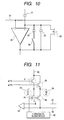
- the mode selection switches are provided in series to respective feedback capacitors, it is also possible to perform such design that the switch 27 in series to the feedback capacitor 23 used in a high gain mode is omitted and the sum of two feedback capacitors 22 and 23 may become desired capacitance at the time of a low gain as shown in FIG. 10.
- the switch 26 in series to the capacitor 22 is turned off. At this time, the gain becomes a value calculated in the formula of (capacitance of capacitor 21/capacitance of capacitor 23).
- the switch 26 is turned on in the "low gain mode.” At this time, the gain becomes a value calculated in the formula of (capacitance of capacitor 21/(capacitance of capacitor 22 + capacitance of capacitor 23)).
- the capacitor 22 and capacitor 23 It is possible to perform the gain design of the "high gain mode” and "low gain mode” by designing the capacitor 22 and capacitor 23. This method can make an area of full capacitative elements small. In addition, it is possible to provide, for example, three or more capacitors and switches, and to have three or more modes.
- the third mode can be used as a super-high gain mode at the time of moving images, or a super-high gain mode at the time of static image pickup at a dark place.
- a feedback type amplifier is used as the variable gain column amplifier here, a feedback type amplifier using a capacitor is preferable as the feedback type amplifier.
- the feedback type amplifier using a capacitor when resistance is small, a current value becomes large and consumed power becomes large, and when resistance is large, not only noise becomes large, but also response deteriorates.
- the feedback type amplifier using a capacitor is more preferable.
- FIG. 4 is a circuit diagram showing an example of the signal adder circuit 3. Since two pixels are added respectively in both of a column direction and a row direction in this embodiment, capacitative elements 31, 32, 33 and 34 and switching devices 35, 36, 37 and 38 for two pixels of each column are provided. Switches 40 and 41 are switched outputting signals of respective columns, and a switch 39 is an addition readout switch which short-circuits between adjacent columns. At the time of addition readout, the switch 39 and switch 40 are turned ON and the switch 41 is turned OFF, and in the readout without addition, the switches 40 and 41 are turned ON and the switch 39 is turned OFF. Since signals in the same color are added in color image pickup, "two pixels in a column direction" and "two pixels in a row direction” are to add adjacent signals every one column or every one row in a color filter with a normal Bayer color array.
- FIG. 5 is a detail drawing of the analog memory cell 4. This diagram shows a circuit for 2 bits.
- the signals passing through the adder circuit are written in the memory capacitors 53 and 54 through memory write switches 51 and 52. Through the memory selecting switches 55 and 56, the written signals are detected as the change of gate potential of memory amplifying transistors 57 and 58, and are outputted.
- FIG. 11 is a diagram showing the structure of an example of the output circuit 5.
- Signal readout from a memory cell of the analog memory cell 4 (here, signal readout from one pixel in FIG. 5 will be explained) is performed by making the transistor 56 turned on.
- An output of the selected memory cell is read in a vertical memory output line 80, and is sampled by a storage capacitor 83 through a switching transistor 81.
- an inversed input terminal and an output terminal of a column amplifier are shortcircuited, and an offset of the variable gain column amplifier 2 is written in a memory cell.
- the readout and sampling of the offset written in the memory cell are the same as the readout and sampling of a signal written in the memory cell.
- the sampling of the offset output from a memory cell to the storage capacitor 84 is performed by applying a pulse ⁇ TN to a switching transistor 82.
- a voltage on the storage capacitor 83 includes an offset of the amplifying transistor 58 in addition to the amplified pixel signal and the offset of the variable gain column amplifier 2.
- a voltage on the storage capacitor 84 includes an offset of the amplifying transistor 58 in addition to the offset of the variable gain column amplifier 2.
- the horizontal scan succeedingly carried out to the above-mentioned operation is performed by a horizontal scan circuit 90.
- the horizontal scan circuit 90 scans the transistor 85 and transistor 86 which are a switch pair, and transfers the voltages on the storage capacitors 83 and 84 to horizontal output lines 87 and 88, respectively.
- a differential amplifier 89 removes an offset between the variable gain column amplifier 2 and amplifying transistor 58, and outputs a sensor signal with a high signal-to-noise ratio.
- FIG. 6 is a signal adder circuit diagram of a solid-state image pickup device of a second embodiment of the present invention.
- FIG. 6 shows an adder circuit diagram in the case of adding three pixels in the column direction and three pixels in the row direction in the solid-state image pickup device having the same block diagram as the first embodiment.
- effective pixel count at the time of static image pickup is 5 million pixels and pixel count at the time of moving image pickup is 300,000 pixels, and hence, high definition still image pickup and 300,000 pixels sufficient for the moving image pickup are secured.
- 3 x 3 9 pixels are added in about 2,700,000 pixels in a central portion at the time of signal addition, and the remaining pixels of a peripheral portion is not used.
- three columns of signals to be added are three rows every other column so that addition of the same color signals may be performed.
- an n-th column, an (n + 2)-th column and an (n + 4)-th column are added.
- an n-th column of signal, an (n + 2)-th column of signal, and an (n + 4)-th column of signal are inputted into signal inputs Sig1, Sig2, and Sig3, respectively.
- the same units in the first embodiment can be used as the other units in this embodiment. Just the number of bits of analog memory cell required for moving images is secured.
- the solid-state image pickup device can be provided on the same semiconductor substrate in each of the above-mentioned embodiments, the differential amplifier 33 may be provided out of the substrate lest noise generated by the differential amplifier 33 should influence other circuit members.
- FIG. 8 is a block diagram showing the case of applying the solid-state image pickup device according to the present invention to the "still camera" corresponding to moving images.
- FIG. 8 shows a barrier 101 which serves as both of a protection of a lens and a main switch, a lens 102 which images an optical image of an object on a solid state image pickup element (solid-state image pickup device) 104, a diaphragm 103 for making the amount of light, which passes through the lens 102, variable, a solid state image pickup element 104 for fetching the object, which is imaged by the lens 102, as an image signal, an A/D converter 106 which performs the analog-to-digital conversion of the image signal outputted from the solid state image pickup element 104, a signal processing unit 107 which performs various kinds of correction to image data outputted from the A/D converter 106, or compresses data, a timing generator 108 which outputs various timing signals to the image pickup element 104, pickup image signal processing circuit 105, A/D converter 106, and signal processing unit 107, a controlling unit 109 for controlling whole and arithmetic operation which controls various calculations and the whole still video camera, a memory
- the controlling unit 109 for controlling whole and arithmetic operation makes the diaphragm 103 open, and a signal outputted from the image pickup element 104 is converted by the A/D converter 106, and thereafter, is inputted into the signal processing unit 107.
- the controlling unit 109 for controlling whole and arithmetic operation calculates exposure on the basis of the data.
- the controlling unit 109 for controlling whole and arithmetic operation controls the diaphragm according to the result.
- the controlling unit 109 for controlling whole and arithmetic operation fetches a high frequency component on the basis of the signal outputted from the image pickup element 104, and calculates the distance to the object. Then, the controlling unit 109 determines whether it is in focus when the lens is driven, and when determining that it is not in focus, the controlling unit 109 drives the lens again and performs ranging. Then, after focusing is confirmed, actual exposure starts.
- the A/D conversion of the image signal outputted from the image pickup element 104 is performed by the A/D converter 106, and is written in the memory unit 110 through the signal processing unit 107 by the controlling unit 109 for controlling whole and arithmetic operation.
- the data accumulated in the memory unit 110 is recorded on the recording medium 112 such as semiconductor memory, which can be detached and attached, through the I/F unit 111 for controlling a recording medium under the control of the controlling unit 109 for controlling whole and arithmetic operation.
- the recording medium 112 such as semiconductor memory
- an image may be inputted directly into a computer or the like through the external I/F unit 113, and may be also processed.
- FIG. 9 is a block diagram showing the case that the solid-state image pickup device of the present invention is applied to a video camera, and an image pickup lens 401 is provided with a focus lens 401A for adjusting a focus, a zoom lens 401B which performs zooming operation, and a lens 401C for imaging.
- the figure shows a diaphragm 402, a solid state image pickup element (solid-state image pickup device) 403 which performs the photoelectric conversion of an object image, which is imaged on an imaging plane, into an electric imaging signal, and a sample/hold circuit (S/H circuit) 404 which performs the sample/hold of the imaging signal outputted from the solid state image pickup element 403, further, amplifies a level, and outputs a picture signal.
- solid state image pickup element solid-state image pickup device
- S/H circuit sample/hold circuit
- a process circuit 405 which performs the predetermined processing such as gamma correction, color separation, and blanking processing to the picture signal outputted from the sample/hold circuit 404 outputs a luminance signal Y and a chroma signal C.
- the chroma signal C outputted from the process circuit 405 is given white balance and color balance in a color signal correction circuit 421, and is outputted as color-difference signals R-Y and B-Y.
- the luminance signal Y outputted from the process circuit 405 and the color-difference signals R-Y and B-Y outputted from the color signal correction circuit 421 are modulated in an encoder circuit (ENC circuit) 424, and is outputted as a standard television signal. Then, the signal is supplied to a VCR or a monitor EVF such as an electronic viewfinder, which is not shown.
- EVC circuit encoder circuit
- an iris control circuit 406 controls an iris drive circuit 407 on the basis of the picture signal supplied from the sample/hold circuit 404, and automatically controls an ig meter so as to control the opening amount of the diaphragm 402 so that a level of the picture signal may become a constant value at a predetermined level.
- Band pass filters (BPF) 413 and 414 having different pass bands extract high frequency components necessary for performing focusing detection from the picture signal outputted from the sample/hold circuit 404.
- Signals outputted from a first band pass filter 413 (BPF1) and a second band pass filter 414 (BPF2) are gated respectively by a gate circuit 415 with a focus gate frame signal, and is inputted into a logic control circuit 417 with a peak value being detected and held in a peak detection circuit 416.
- This signal is called a focus voltage, and a focus is adjusted with this focus voltage.
- other relating units are a focal encoder 418 which detects a moving position of the focus lens 401A, a zoom encoder 419 which detects the focal length of the zoom lens 401B, and an iris encoder 420 which detects the opening amount of the diaphragm 402. Detection values of these encoders are supplied to the logic control circuit 417 which performs system control. The logic control circuit 417 performs focus detection to an object on the basis of the picture signal corresponding to a set focus detection region, and adjusts a focus.
- the logic control circuit 417 fetches the information of peak values of high frequency components supplied from respective band pass filters 413 and 414, supplies control signals of a rotation direction, rotational speed, rotation/stop, and the like of a focus motor 410 to the focusing driver circuit 409 so as to drive the focus lens 401A to a position where the peak values of high frequency components become maximum, and controls this.
- the present invention is applied to a solid-state image pickup device in which a plurality of pixels are arranged two-dimensionally, and has means of reading a signal which is given photoelectric conversion by a pixel, and is used suitably for a digital camera (still camera) corresponding to moving images, a digital video camera, and the like.
- the present invention achieves a high S/N, and achieves a solid-state image pickup device suitable for both of static image pickup and moving image pickup.
- the solid-state image pickup device is a solid-state image pickup device which has a pixel unit has a plurality of pixels which are arranged two-dimensionally and output pixel signals derived by a photoelectric conversion, and is provided with a first mode of reading a pixel signal every pixel, and a second mode of adding and reading a plurality of pixel signals, having a variable gain column amplifier for performing readout at different gains in the first mode and second mode.
- the solid-state image pickup device has a plurality of output lines where output signals from a plurality of pixels arranged in one line are outputted respectively, and at least one of the variable gain amplifier is connected to each of the plurality of output lines.
- a gain at the time of readout in the second mode is made to be higher than a gain at the time of readout in the first mode.
Abstract
Description
- The present invention relates to a solid-state image pickup device and an image pickup system, and in particular, to a CMOS type solid-state image pickup device and a camera, which are adapted for both static image pickup and moving image pickup.
- In recent years, with being characterized in that a CMOS type solid-state image pickup device is low in power consumption and easy to be accelerated in comparison with a CCD (Charge Coupled Device), the CMOS type solid-state image pickup device begins to spread quickly as an image sensor for a portable device, or for a single-lens reflex camera which perform high-speed rapid shooting.
- In order for a CMOS type solid-state image pickup device to spread further, the engineering development which can perform still image pickup and moving image pickup in high definition is required.
- Heretofore, in a MOS type solid-state image pickup device, a method of performing high-definition static image pickup and moving image pickup using analog memory cell provided in an image pickup device is described in Japanese Patent Application Laid-Open No. H02-65380 which is a Japanese patent. According to this invention, in the MOS type solid-state image pickup device, the following disclosure is performed as a method of suppressing the blurring of an image which the time difference of image pickup between an even number field and an odd number field generates. Analog memory cell besides a pixel unit is provided, and a signal obtained by photoelectric conversion in the pixel unit is once transferred per line to memory means. Then, after that, the timing difference of charge storage between the odd number field and even number field is made small by transferring a store signal of the memory means concerned by turns to an output signal line. In this invention, memory is used in order to enhance image quality at the time of still image pickup, and memory has the number of bits corresponding to full pixels. On the other hand, it is made that moving image pickup is performed at a video rate without going through memory.
- It becomes hard to perform readout at the video rate at the time of moving image pickup as the pixel count of a still image increases. For example, supposing the pixel count of 3 million pixels or more is necessary in high-definition static image pickup, it is necessary to perform readout at speed of 90 MHz so as to perform readout at intervals of 1/30 sec. Then, a method of reducing the pixel count of moving images with the pixel count of a still image being maintained has been studied. One method of them is pixel addition, that is, a method of adding a plurality of photoelectric conversion signals, and decreasing the pixel count to be read.
- An example of the pixel addition method in a CMOS type solid-state image pickup device is described in Japanese Patent Application Laid-Open No. H09-247535 which is a Japanese patent. What is described in this invention is a method of the memory consisting of a switching device and a capacitative element for every readout line from pixels is provided for multiple lines, and outputting an average of a plurality of stored signals by turning on concurrently switching devices of a plurality of stored signals to be added. In this way, in the CMOS type solid-state image pickup device, "pixel addition" is equivalent to "pixel averaging." In this invention, an effect of decreasing random noise by averaging read signals after reading the same pixel signal multiple times is described. By using the same structure, it becomes possible to read the signal in the pixel count, which is smaller than the case that an unnecessary signal is skipped by averaging other pixel signals, in low random noise and low fixed pattern noise. Owing to this method, in comparison with the case of no addition, both of the random noise and fixed pattern noise become:
- In addition, a solid-state image pickup device which is provided with an amplifier with a gain exceeding 1 in each column is disclosed in Japanese Patent Application No. 2003-51989 which is a Japanese patent.
- In view of the above-mentioned conventional examples, what is conceivable is the structure of reading only the pixel count necessary for using addition means when the pixel count increases in an image pickup apparatus where analog memory cell is mounted. In that case, the following subjects arise in extension of conventional inventions.
- (1) When the pixel count increases, the readout through memory becomes more important in moving images rather than in a still image. In moving images, there also exist restrictions of formats in an output device, and large pixel count is unnecessary. The new structure that a still image and moving images are imaged in high definition with a mega-pixel-class image pickup apparatus is necessary.
- (2) Since the pixel addition, that is, the averaged readout makes the random noise of pixels small, an S/N improves. Nevertheless, in CCD technology, not only random noise becomes small, but also a signal component becomes large. Thus, in the CCD, a charge number is added by add operation and a value of an S of the S/N also becomes large. Owing to this, in consideration of a CCD, new means of improving the S/N in the readout method of adopting the add operation is demanded in a CMOS type solid-state image pickup device.
-
- In order to solve the above-mentioned subjects, a solid-state image pickup device of the present invention is a solid-state image pickup device which has a plurality of pixels which are arranged two-dimensionally and output pixel signals derived by a photoelectric conversion, and an output line which outputs an output signal per the plurality of above-mentioned pixels arranged in one line, and is provided with a first mode of reading the above-mentioned output signal every pixel, and a second mode of adding and reading the output signals from the plurality of pixels, wherein a gain at the time of readout in the above-mentioned second mode is made to be higher than a gain at the time of readout in the above-mentioned first mode by variable gain amplifying means at least one of which is connected to each of the plurality of above-mentioned output lines.
- In the above-mentioned solid-state image pickup device of the present invention, it is desirable to have analog memory cell which keeps a signal after addition during one frame, to make a gain at the time of performing readout in a mode of adding and reading pixel signals higher than a gain at the time of reading a pixel signal in a mode of directly reading, to have a plurality of output lines where output signals from a plurality of pixels arranged in one line are outputted respectively, and to connect at least one of the above-mentioned variable gain amplifying means to each of the plurality of above-mentioned output lines, or to make a mode of reading a signal directly an operation mode of readout of a still image and to make a mode of adding and reading a plurality of signals a mode of readout of moving images.
- A reason why the S/N and dynamic range in both modes can be optimized by performing switching so that the gain in the mode of addition may become higher in the mode of adding the plurality of pixel signals and the mode of no addition (mode of reading a signal per pixel) will be explained below.
- FIG. 7 is a model diagram for calculating the S/N of a circuit reading from a pixel unit. Let a light signal from the pixel unit be S1, let a noise signal of the pixel unit be N1, let again of gain means be G, and let the noise of a subsequent stage of circuit be N2, and each of the light signal S and noise signal N of an output signal is:
- Hence,
- Then, in the image pickup that exposure time is controllable and sufficient light amount is obtained, for example like a still image, an image is read at a relatively low gain so as to secure a dynamic range. In the image pickup that sufficient light amount is not obtained, that is, moving images or a still image in a dark environment, a method of reading them or it at a relatively high gain is effective so as to secure the S/N.
- In this way, it is possible to obtain an image pickup apparatus which obtains high image quality in both of static image pickup and moving image pickup by applying readout gains which are different at the time of addition readout and at the time of normal readout.
- In addition, at the time of moving image pickup, an output signal obtained by addition is transferred at high speed, and is made to be accumulated in analog memory cell. It is appropriate that the number of bits of the analog memory cell is equal to the pixel count necessary for moving images. It is possible to suppress the increase of a chip area because of mounting memory to a minimum by preparing only necessary analog memory cell.
- It is possible to apply a gain directly to a signal of a pixel unit by adopting the structure of one gain means being provided per line corresponding to a readout line, a so-called column amplifier, and hence, it is possible to suppress the noise N2 in the subsequent stage which is shown in the formula shown above.
- According to the present invention, it becomes possible to provide a solid-state image pickup device which can perform image pickup at the higher S/N under an environment such as low illuminance at the time of pixel addition, and can perform image pickup at the high S/N with a wide dynamic range under a comparatively high illuminance usually (at the time of no pixel addition), compatibly.
- In addition, it is possible to provide a solid-state image pickup device suitable for both static image pickup and moving image pickup by using the pixel addition mode at the time of moving image pickup or at the time of relatively low illuminance image pickup, and using the normal mode for image pickup in a still image mode.
-
- FIG. 1 is a configuration block diagram of a solid-state image pickup device of a first embodiment of the present invention;
- FIG. 2 is a diagram showing a pixel circuit of the solid-state image pickup device of the above-mentioned first embodiment;
- FIG. 3 is a circuit diagram of a variable gain column amplifier of the solid-state image pickup device of the above-mentioned first embodiment;
- FIG. 4 is an adder circuit diagram of the solid-state image pickup device of the above-mentioned first embodiment;
- FIG. 5 is a circuit diagram of an analog memory cell unit of the solid-state image pickup device of the above-mentioned first embodiment;
- FIG. 6 is an adder circuit diagram of the solid-state image pickup device of a second embodiment of the present invention;
- FIG. 7 is a model diagram for calculating an S/N of a readout circuit from a pixel unit;
- FIG. 8 is a block diagram showing the case that the solid-state image pickup device according to the present invention is applied to a still video camera corresponding to moving images;
- FIG. 9 is a block diagram showing the case that the solid-state image pickup device of the present invention is applied to a video camera;
- FIG. 10 is a circuit diagram of another variable gain column amplifier of the solid-state image pickup device of the above-mentioned first embodiment; and
- FIG. 11 is a diagram showing the structure of an example of an output circuit 5 in FIG. 1.
-
- Hereafter, embodiments of the present invention will be explained in detail using drawings.
- FIG. 1 is a block diagram of a solid-state image pickup device of a first embodiment of the present invention. A pixel output signal outputted from each output line of a
pixel array 1 located two-dimensionally is amplified at a suitable gain by a variablegain column amplifier 2 used as variable gain amplifying means. Aninput capacitor 21 not only plays the role of clamping noise in a dark environment, but also plays the role of determining a gain by a capacitance ratio betweenfeedback capacitors gain column amplifier 2 are not only connected through thefeedback capacitor 22 and aswitch 26, but also connected through thefeedback capacitor 23 and aswitch 27. It is possible to select a gain by switching theswitches - Clamping operation by the
input capacitor 21 sets an input side of adifferential amplifier 25 of theinput capacitor 21 at a reference voltage of areference voltage input 24 by turning on aswitch 28. In the state, atransistor 204 for resetting resets a gate electrode of an amplifyingtransistor 203 of a pixel shown in FIG. 2 at predetermined electric potential, and noise from the pixel is inputted into theinput capacitor 21. Then, theswitch 28 is turned off, the input side of thedifferential amplifier 25 of theinput capacitor 21 is made to float, a light signal is sent to the gate electrode of the amplifyingtransistor 203 through acharge transfer transistor 202 from aphotodiode 201 in a pixel, and the amplified signal is inputted from the pixel into theinput capacitor 21. The amount of electric potential change of the input terminal of theinput capacitor 21 becomes the amount obtained by removing a noise component from the signal, and the signal that the noise is reduced is made to be inputted into the variablegain column amplifier 2. - A switching signal of gains can be generated by a timing generator inside a sensor, and further, can be also generated from a camera system or a video system. Generally, it is preferable to transmit a mode switching signal from a communication terminal of a camera system or a video system and to control a sensor directly or through a timing generator. Although a user switches gains with a switch or the like generally, it is also possible to detect a motion of an object and to perform switching, for example, in an application of a surveillance camera or the like. With explaining a still camera shown in FIG. 8 described later as an example, a gain switching command signal is sent with a switch, not shown, to a controlling
unit 109 for controlling whole and arithmetic operation. Then, a gain switch signal is sent to theswitches timing generator 108. - After passing through the variable
gain column amplifier 2, the signal is inputted into a signal adder circuit 3 as required. Plural columns of signal lines are inputted into input terminals of the signal adder circuit 3 according to the pixel count added in a column direction. In the signal adder circuit 3, the readout (readout without addition) per pixel and the addition readout in the plurality of pixel signals are switched. In addition, the signal adder circuit 3 is constituted of a plurality of capacitance means and a plurality of switches. The signal passing through the signal adder circuit 3 is stored in analog memory cell 4 as required. The number of bits of the analog memory cell may be equal to the number of signals after addition. For example, in the embodiment, it is made that full effective pixel count is 3,200,000 pixels, and analog memory cell is for 800,000 pixels. Thus, in the signal adder circuit, the signals for 4 pixels are added to make one output signal. The signal which passes through the memory 4 is outputted out of a chip from an output circuit 5 which is constituted of a horizontal output line and differential amplifier circuits. The differential amplifier circuits are effective in removing the offset dispersion among a plurality of variablegain column amplifiers 2. In addition, a horizontal scan circuit 6 which scans horizontally thepixel unit 1, signal adder circuit 3, analog memory cell 4, and output circuit 5, avertical scan circuit 7 which scans thepixel unit 1 vertically, and the like are located besides these in the chip. - FIG. 2 is a unit pixel circuit diagram of the
pixel unit 1. The light signal which is given photoelectric conversion by thephotodiode 201 is transferred to the gate electrode of the amplifyingtransistor 203 by thecharge transfer transistor 202. A pixel selected by a selectingtransistor 205 outputs output potential according to the gate potential of the amplifying transistor to asignal output line 206. The gate electrode of the amplifyingtransistor 203 is reset at the predetermined electric potential by thetransistor 204 for resetting. Although the pixel explained here is what is called a CMOS sensor, the pixel is not limit to the CMOS sensor especially, but a VMIS (Threshold Voltage Modulation Image Sensor), a BCAST (Buried Charge Accumulator and Sensing Transistor array), an LBCAST (Lateral Buried Charge Accumulator and Sensing Transistor array) or the like is applicable. In particular, as for the BCAST and LBCAST, it is possible to achieve the replacement without being accompanied by essential modification by replacing JFET transistors with the amplifying MOS transistors. In addition, it is possible to use a type of sensor of leading signal charges accumulated in a photoelectric conversion unit to a control electrode of a transistor with which a pixel is provided, and outputting an amplified signal from a main electrode, for the pixel of this embodiment. Its examples are a SIT type image sensor using a SIT as the amplifying transistor (A. Yusa, J. Nishizawa et al., "SIT image sensor: Design consideration and characteristic, " IEEE trans. Vol. ED-33, pp. 735-742, June 1986), a BASIS using a bipolar transistor (N. Tanaka et al., "A 310 K pixel bipolar imager (BASIS))," IEEE Trans. Electron Devices, vol. 35, pp. 646-652, May 1990), a CMD using a JFET which a control electrode is depleted (Nakamura et. al., "Gate accumulation type MOS phototransistor image sensor," Proceedings of ITE, 41, 11, pp. 1075-1082, Nov. 1987), and the like. - FIG. 3 is a diagram showing an example of the variable gain column amplifier circuit. An output signal from a pixel is clamped by the
input capacitor 21, and becomes a differential input of thedifferential amplifier 25 with thereference voltage input 24. Themode selection switch 26 is located in series to thefeedback capacitor 22 for a low gain and themode selection switch 27 is located in series to thefeedback capacitor 23 for a high gain, and a gain of thedifferential amplifier 25 is selected by either being turned on. In addition, thereset switch 28 which triggers a reset by making the input and output of the amplifier into the same potential is located in parallel to thefeedback capacitors switch 27 in series to thefeedback capacitor 23 used in a high gain mode is omitted and the sum of twofeedback capacitors switch 26 in series to thecapacitor 22 is turned off. At this time, the gain becomes a value calculated in the formula of (capacitance ofcapacitor 21/capacitance of capacitor 23). Theswitch 26 is turned on in the "low gain mode." At this time, the gain becomes a value calculated in the formula of (capacitance ofcapacitor 21/(capacitance ofcapacitor 22 + capacitance of capacitor 23)). It is possible to perform the gain design of the "high gain mode" and "low gain mode" by designing thecapacitor 22 andcapacitor 23. This method can make an area of full capacitative elements small. In addition, it is possible to provide, for example, three or more capacitors and switches, and to have three or more modes. The third mode can be used as a super-high gain mode at the time of moving images, or a super-high gain mode at the time of static image pickup at a dark place. Although a feedback type amplifier is used as the variable gain column amplifier here, a feedback type amplifier using a capacitor is preferable as the feedback type amplifier. For example, in a feedback type amplifier using a resistor, when resistance is small, a current value becomes large and consumed power becomes large, and when resistance is large, not only noise becomes large, but also response deteriorates. When this point is taken into consideration, the feedback type amplifier using a capacitor is more preferable. - FIG. 4 is a circuit diagram showing an example of the signal adder circuit 3. Since two pixels are added respectively in both of a column direction and a row direction in this embodiment,
capacitative elements devices Switches switch 39 is an addition readout switch which short-circuits between adjacent columns. At the time of addition readout, theswitch 39 and switch 40 are turned ON and theswitch 41 is turned OFF, and in the readout without addition, theswitches switch 39 is turned OFF. Since signals in the same color are added in color image pickup, "two pixels in a column direction" and "two pixels in a row direction" are to add adjacent signals every one column or every one row in a color filter with a normal Bayer color array. - FIG. 5 is a detail drawing of the analog memory cell 4. This diagram shows a circuit for 2 bits. The signals passing through the adder circuit are written in the
memory capacitors memory selecting switches memory amplifying transistors - FIG. 11 is a diagram showing the structure of an example of the output circuit 5. Signal readout from a memory cell of the analog memory cell 4 (here, signal readout from one pixel in FIG. 5 will be explained) is performed by making the
transistor 56 turned on. An output of the selected memory cell is read in a verticalmemory output line 80, and is sampled by astorage capacitor 83 through a switchingtransistor 81. Next, an inversed input terminal and an output terminal of a column amplifier are shortcircuited, and an offset of the variablegain column amplifier 2 is written in a memory cell. The readout and sampling of the offset written in the memory cell are the same as the readout and sampling of a signal written in the memory cell. The sampling of the offset output from a memory cell to thestorage capacitor 84 is performed by applying a pulse ϕTN to a switchingtransistor 82. A voltage on thestorage capacitor 83 includes an offset of the amplifyingtransistor 58 in addition to the amplified pixel signal and the offset of the variablegain column amplifier 2. A voltage on thestorage capacitor 84 includes an offset of the amplifyingtransistor 58 in addition to the offset of the variablegain column amplifier 2. - The horizontal scan succeedingly carried out to the above-mentioned operation is performed by a
horizontal scan circuit 90. Thehorizontal scan circuit 90 scans thetransistor 85 andtransistor 86 which are a switch pair, and transfers the voltages on thestorage capacitors horizontal output lines differential amplifier 89 removes an offset between the variablegain column amplifier 2 and amplifyingtransistor 58, and outputs a sensor signal with a high signal-to-noise ratio. - FIG. 6 is a signal adder circuit diagram of a solid-state image pickup device of a second embodiment of the present invention. FIG. 6 shows an adder circuit diagram in the case of adding three pixels in the column direction and three pixels in the row direction in the solid-state image pickup device having the same block diagram as the first embodiment. In this embodiment, it is made that effective pixel count at the time of static image pickup is 5 million pixels and pixel count at the time of moving image pickup is 300,000 pixels, and hence, high definition still image pickup and 300,000 pixels sufficient for the moving image pickup are secured. What is adopted is such structure that 3 x 3 = 9 pixels are added in about 2,700,000 pixels in a central portion at the time of signal addition, and the remaining pixels of a peripheral portion is not used.
- Similarly to the first embodiment, three columns of signals to be added are three rows every other column so that addition of the same color signals may be performed. Thus, an n-th column, an (n + 2)-th column and an (n + 4)-th column are added. In FIG. 6, an n-th column of signal, an (n + 2)-th column of signal, and an (n + 4)-th column of signal are inputted into signal inputs Sig1, Sig2, and Sig3, respectively. Assuming three lines to be added are an m-th line, an (m + 2)-th line, and an (m + 4)-th line, when the m-th line of signal is first inputted as signals Sig1, Sig2, and Sig3, switches 61, 62, and 63 are turned ON and switches 64, 65, and 66 are turned ON. Hence, the signal (m, n), signal (m, n + 2), and signal (m, n + 4) are written in
retention capacitors switches switches signal retention capacitor 73 by turning aswitch 70 ON. - Next, when the (m + 2)-th line of signals are inputted as signals Sig1, Sig2 and Sig3, similarly to the m-th line of signals, a signal (m + 2, n), a signal (m + 2, n + 2), and a signal (m + 2, n + 4) are kept in the
retention capacitors signal retention capacitor 74 by turning on aswitch 71. - Similarly, the added result of the signals (m + 4, n), (m + 4, n + 2), and (m + 4, n + 4) is written in an added
signal retention capacitor 75. - Then, the signals currently written in three added
signal retention capacitors switches source follower amplifier 79. - The same units in the first embodiment can be used as the other units in this embodiment. Just the number of bits of analog memory cell required for moving images is secured.
- In addition, although the solid-state image pickup device can be provided on the same semiconductor substrate in each of the above-mentioned embodiments, the
differential amplifier 33 may be provided out of the substrate lest noise generated by thedifferential amplifier 33 should influence other circuit members. - On the basis of FIG. 8, one embodiment in the case of applying a solid-state image pickup device relating to the present invention to a still camera (image pickup system) corresponding to moving images will be explained in detail.
- FIG. 8 is a block diagram showing the case of applying the solid-state image pickup device according to the present invention to the "still camera" corresponding to moving images.
- FIG. 8 shows a barrier 101 which serves as both of a protection of a lens and a main switch, a lens 102 which images an optical image of an object on a solid state image pickup element (solid-state image pickup device) 104, a diaphragm 103 for making the amount of light, which passes through the lens 102, variable, a solid state image pickup element 104 for fetching the object, which is imaged by the lens 102, as an image signal, an A/D converter 106 which performs the analog-to-digital conversion of the image signal outputted from the solid state image pickup element 104, a signal processing unit 107 which performs various kinds of correction to image data outputted from the A/D converter 106, or compresses data, a timing generator 108 which outputs various timing signals to the image pickup element 104, pickup image signal processing circuit 105, A/D converter 106, and signal processing unit 107, a controlling unit 109 for controlling whole and arithmetic operation which controls various calculations and the whole still video camera, a memory unit 110 for storing image data temporarily, an interface unit 111 for performing record to or readout from a recording medium, a recording medium 112 which can be detached and attached like semiconductor memory for performing the record or readout of image data, and an interface unit 113 for communicating with an external computer and the like.
- Next, the operation of a still video camera at the time of image pickup in the above-mentioned structure will be explained.
- When the
barrier 101 is opened, main power is turned on, then, the power supply of a control system is turned on, and further, the power supply of imaging system circuits such as the A/D converter 106 is turned on. - Then, in order to control exposure, the controlling
unit 109 for controlling whole and arithmetic operation makes thediaphragm 103 open, and a signal outputted from theimage pickup element 104 is converted by the A/D converter 106, and thereafter, is inputted into thesignal processing unit 107. The controllingunit 109 for controlling whole and arithmetic operation calculates exposure on the basis of the data. - After determining brightness with the result of this metering, the controlling
unit 109 for controlling whole and arithmetic operation controls the diaphragm according to the result. - Next, the controlling
unit 109 for controlling whole and arithmetic operation fetches a high frequency component on the basis of the signal outputted from theimage pickup element 104, and calculates the distance to the object. Then, the controllingunit 109 determines whether it is in focus when the lens is driven, and when determining that it is not in focus, the controllingunit 109 drives the lens again and performs ranging. Then, after focusing is confirmed, actual exposure starts. - When the exposure is completed, the A/D conversion of the image signal outputted from the
image pickup element 104 is performed by the A/D converter 106, and is written in thememory unit 110 through thesignal processing unit 107 by the controllingunit 109 for controlling whole and arithmetic operation. - Then, the data accumulated in the
memory unit 110 is recorded on therecording medium 112 such as semiconductor memory, which can be detached and attached, through the I/F unit 111 for controlling a recording medium under the control of the controllingunit 109 for controlling whole and arithmetic operation. - In addition, an image may be inputted directly into a computer or the like through the external I/
F unit 113, and may be also processed. - Furthermore, on the basis of FIG. 9, an example of the case of applying a solid-state image pickup device of the present invention to a video camera will be explained in detail.
- FIG. 9 is a block diagram showing the case that the solid-state image pickup device of the present invention is applied to a video camera, and an
image pickup lens 401 is provided with afocus lens 401A for adjusting a focus, azoom lens 401B which performs zooming operation, and alens 401C for imaging. - Moreover, the figure shows a
diaphragm 402, a solid state image pickup element (solid-state image pickup device) 403 which performs the photoelectric conversion of an object image, which is imaged on an imaging plane, into an electric imaging signal, and a sample/hold circuit (S/H circuit) 404 which performs the sample/hold of the imaging signal outputted from the solid stateimage pickup element 403, further, amplifies a level, and outputs a picture signal. - A
process circuit 405 which performs the predetermined processing such as gamma correction, color separation, and blanking processing to the picture signal outputted from the sample/hold circuit 404 outputs a luminance signal Y and a chroma signal C. The chroma signal C outputted from theprocess circuit 405 is given white balance and color balance in a colorsignal correction circuit 421, and is outputted as color-difference signals R-Y and B-Y. - In addition, the luminance signal Y outputted from the
process circuit 405 and the color-difference signals R-Y and B-Y outputted from the colorsignal correction circuit 421 are modulated in an encoder circuit (ENC circuit) 424, and is outputted as a standard television signal. Then, the signal is supplied to a VCR or a monitor EVF such as an electronic viewfinder, which is not shown. - Next, an
iris control circuit 406 controls an iris drive circuit 407 on the basis of the picture signal supplied from the sample/hold circuit 404, and automatically controls an ig meter so as to control the opening amount of thediaphragm 402 so that a level of the picture signal may become a constant value at a predetermined level. Band pass filters (BPF) 413 and 414 having different pass bands extract high frequency components necessary for performing focusing detection from the picture signal outputted from the sample/hold circuit 404. Signals outputted from a first band pass filter 413 (BPF1) and a second band pass filter 414 (BPF2) are gated respectively by agate circuit 415 with a focus gate frame signal, and is inputted into alogic control circuit 417 with a peak value being detected and held in apeak detection circuit 416. - This signal is called a focus voltage, and a focus is adjusted with this focus voltage. In addition, other relating units are a
focal encoder 418 which detects a moving position of thefocus lens 401A, azoom encoder 419 which detects the focal length of thezoom lens 401B, and aniris encoder 420 which detects the opening amount of thediaphragm 402. Detection values of these encoders are supplied to thelogic control circuit 417 which performs system control. Thelogic control circuit 417 performs focus detection to an object on the basis of the picture signal corresponding to a set focus detection region, and adjusts a focus. Thus, thelogic control circuit 417 fetches the information of peak values of high frequency components supplied from respective band pass filters 413 and 414, supplies control signals of a rotation direction, rotational speed, rotation/stop, and the like of a focus motor 410 to the focusingdriver circuit 409 so as to drive thefocus lens 401A to a position where the peak values of high frequency components become maximum, and controls this. - The present invention is applied to a solid-state image pickup device in which a plurality of pixels are arranged two-dimensionally, and has means of reading a signal which is given photoelectric conversion by a pixel, and is used suitably for a digital camera (still camera) corresponding to moving images, a digital video camera, and the like.
- In a solid-state image pickup device which has means of adding signals from a plurality of pixels, the present invention achieves a high S/N, and achieves a solid-state image pickup device suitable for both of static image pickup and moving image pickup. The solid-state image pickup device is a solid-state image pickup device which has a pixel unit has a plurality of pixels which are arranged two-dimensionally and output pixel signals derived by a photoelectric conversion, and is provided with a first mode of reading a pixel signal every pixel, and a second mode of adding and reading a plurality of pixel signals, having a variable gain column amplifier for performing readout at different gains in the first mode and second mode. The solid-state image pickup device has a plurality of output lines where output signals from a plurality of pixels arranged in one line are outputted respectively, and at least one of the variable gain amplifier is connected to each of the plurality of output lines. A gain at the time of readout in the second mode is made to be higher than a gain at the time of readout in the first mode.
Claims (11)
- A solid-state image pickup device which has a plurality of pixels which are arranged two-dimensionally and output pixel signals derived by photoelectric conversion, and an output line which outputs an output signal per the plurality of pixels arranged in one line, and comprises a first mode of reading the output signal every pixel, and a second mode of adding and reading output signals from the plurality of pixels, characterized in that a gain at the time of readout in the second mode is made to be higher than a gain at the time of readout in the first mode by variable gain amplifying means at least one of which is connected to each of the plurality of output lines.
- The solid-state image pickup device according to claim 1, characterized by further comprising analog memory cell which keeps a signal after addition during one frame.
- The solid-state image pickup device according to any one of claims 1 and 2, characterized in that the first mode is made a still image readout operation mode, and the second mode is made a moving image readout mode.
- The solid-state image pickup device according to any one of claims 1 to 3, characterized by further comprising means of inputting a signal from the variable gain amplifying means and outputting a signal every pixel according to the first mode or an added signal according to the second mode by switching the first mode and the second mode.
- The solid-state image pickup device according to any one of claims 1 to 4, characterized in that each output line is connected to the variable gain amplifying means through a coupling capacitor for removing noise of the pixel by clamping a signal from the pixel.
- The solid-state image pickup device according to claim 5, characterized in that, when the coupling capacitor is set as a first coupling capacitor, the variable gain amplifying means is a feedback type amplifier and has a second coupling capacitor, which performs capacity coupling of an output terminal and an input terminal of the amplifier, and a third coupling capacitor, which performs capacity coupling of the output terminal and the input terminal of the amplifier, and that a gain at the time of readout in the first mode is determined by a ratio of the first coupling capacitor and the second coupling capacitor, and a gain at the time of readout in the second mode is determined by a ratio of the first coupling capacitor and the third coupling capacitor.
- The solid-state image pickup device according to claim 2, characterized in that the analog memory cell is a plurality of amplifying type memory cells each of which comprises at least a signal storage capacitor, a transistor for writing a signal, and a transistor for amplifying the signal, and corresponds to at least a part of the plurality of pixels.
- The solid-state image pickup device according to claim 7, characterized by further comprising circuit means which is arranged every column of the amplifying type memory cells of the analog memory cell and outputs an output offset between the variable gain amplifying means and the analog memory cell, and a signal from the analog memory cell.
- The solid-state image pickup device according to claim 8, characterized in that the circuit means comprises a first storage capacitor which accumulates the output offset, a first transfer transistor which transfers the output offset to the first storage capacitor, a second storage capacitor which accumulates a signal from the analog memory cell, and a second transfer transistor which transfers the signal from the analog memory cell to the second storage capacitor.
- The solid-state image pickup device according to claim 9, characterized by further comprising means of subtracting the output offset and the signal from the circuit means.
- A camera, characterized by comprising the solid-state image pickup device according to any one of claims 1 to 10, an optical system which images light to the solid-state image pickup device, and a signal processing circuit which processes an output signal from the solid-state image pickup device.
Priority Applications (1)
| Application Number | Priority Date | Filing Date | Title |
|---|---|---|---|
| EP10183600A EP2271074A2 (en) | 2004-05-20 | 2005-05-19 | Solid-state image pickup device and camera |
Applications Claiming Priority (2)
| Application Number | Priority Date | Filing Date | Title |
|---|---|---|---|
| JP2004150538A JP4290066B2 (en) | 2004-05-20 | 2004-05-20 | Solid-state imaging device and imaging system |
| JP2004150538 | 2004-05-20 |
Publications (2)
| Publication Number | Publication Date |
|---|---|
| EP1599032A2 true EP1599032A2 (en) | 2005-11-23 |
| EP1599032A3 EP1599032A3 (en) | 2007-08-01 |
Family
ID=34936690
Family Applications (2)
| Application Number | Title | Priority Date | Filing Date |
|---|---|---|---|
| EP10183600A Withdrawn EP2271074A2 (en) | 2004-05-20 | 2005-05-19 | Solid-state image pickup device and camera |
| EP05010858A Withdrawn EP1599032A3 (en) | 2004-05-20 | 2005-05-19 | Solid-state image pickup device and camera |
Family Applications Before (1)
| Application Number | Title | Priority Date | Filing Date |
|---|---|---|---|
| EP10183600A Withdrawn EP2271074A2 (en) | 2004-05-20 | 2005-05-19 | Solid-state image pickup device and camera |
Country Status (4)
| Country | Link |
|---|---|
| US (2) | US7714919B2 (en) |
| EP (2) | EP2271074A2 (en) |
| JP (1) | JP4290066B2 (en) |
| CN (1) | CN100438582C (en) |
Cited By (1)
| Publication number | Priority date | Publication date | Assignee | Title |
|---|---|---|---|---|
| EP2271074A2 (en) | 2004-05-20 | 2011-01-05 | Canon Kabushiki Kaisha | Solid-state image pickup device and camera |
Families Citing this family (54)
| Publication number | Priority date | Publication date | Assignee | Title |
|---|---|---|---|---|
| JP2005328275A (en) * | 2004-05-13 | 2005-11-24 | Canon Inc | Solid state imaging device and imaging system |
| JP4290071B2 (en) * | 2004-06-02 | 2009-07-01 | キヤノン株式会社 | Solid-state imaging device and imaging system |
| JP2005348041A (en) * | 2004-06-02 | 2005-12-15 | Canon Inc | Solid state imaging device and imaging system |
| US7443435B2 (en) * | 2004-07-07 | 2008-10-28 | Altasens, Inc. | Column amplifier with automatic gain selection for CMOS image sensors |
| JP4759293B2 (en) * | 2005-03-15 | 2011-08-31 | キヤノン株式会社 | Image sensor |
| JP4497022B2 (en) * | 2005-04-26 | 2010-07-07 | ソニー株式会社 | Solid-state imaging device, driving method of solid-state imaging device, and imaging device |
| US7561812B2 (en) * | 2005-10-13 | 2009-07-14 | Lite-On Technology Corp. | Optical receiver with matched photodetector capacitance |
| EP1788797B1 (en) * | 2005-11-18 | 2013-06-26 | Canon Kabushiki Kaisha | Solid-state image pickup device |
| JP4723994B2 (en) | 2005-12-19 | 2011-07-13 | 株式会社東芝 | Solid-state imaging device |
| JP4861015B2 (en) * | 2006-01-13 | 2012-01-25 | キヤノン株式会社 | Imaging device and imaging apparatus |
| US8687087B2 (en) * | 2006-08-29 | 2014-04-01 | Csr Technology Inc. | Digital camera with selectively increased dynamic range by control of parameters during image acquisition |
| US7714903B2 (en) | 2006-08-29 | 2010-05-11 | Zoran Corporation | Wide dynamic range image capturing system method and apparatus |
| JP5284521B2 (en) * | 2006-08-31 | 2013-09-11 | キヤノン株式会社 | Photoelectric conversion device, imaging system, and driving method of photoelectric conversion device |
| JP5173171B2 (en) | 2006-09-07 | 2013-03-27 | キヤノン株式会社 | PHOTOELECTRIC CONVERSION DEVICE, IMAGING DEVICE, AND SIGNAL READING METHOD |
| JP4921911B2 (en) * | 2006-09-29 | 2012-04-25 | オリンパス株式会社 | Solid-state imaging device |
| JP2008136047A (en) * | 2006-11-29 | 2008-06-12 | Sony Corp | Solid-state imaging apparatus and imaging apparatus |
| US7990452B2 (en) * | 2007-01-31 | 2011-08-02 | Aptina Imaging Corporation | Apparatus, methods and systems for amplifier |
| JP5255790B2 (en) * | 2007-02-14 | 2013-08-07 | 富士フイルム株式会社 | Imaging device |
| JP2008294913A (en) * | 2007-05-28 | 2008-12-04 | Panasonic Corp | Solid-state imaging apparatus and its driving method |
| JP4673396B2 (en) * | 2007-09-14 | 2011-04-20 | キヤノン株式会社 | Imaging apparatus and imaging system |
| JP2009141631A (en) | 2007-12-05 | 2009-06-25 | Canon Inc | Photoelectric conversion device and image pickup device |
| JP5151507B2 (en) * | 2008-01-29 | 2013-02-27 | ソニー株式会社 | Solid-state imaging device, signal readout method of solid-state imaging device, and imaging apparatus |
| JP2009303088A (en) * | 2008-06-17 | 2009-12-24 | Panasonic Corp | Solid-state imaging device, its driving method and camera |
| JP2010062639A (en) | 2008-09-01 | 2010-03-18 | Canon Inc | Imaging apparatus |
| JP5317591B2 (en) * | 2008-09-01 | 2013-10-16 | キヤノン株式会社 | Imaging device |
| US8300123B2 (en) * | 2008-10-16 | 2012-10-30 | Aptina Imaging Corporation | Imager column-level amplifier with pixel-wise automatic gain selection |
| JP2010147614A (en) * | 2008-12-16 | 2010-07-01 | Panasonic Corp | Solid-state imaging apparatus and method for driving the same, imaging apparatus |
| JP5406554B2 (en) * | 2009-02-20 | 2014-02-05 | キヤノン株式会社 | Imaging apparatus and imaging system |
| WO2010119702A1 (en) * | 2009-04-16 | 2010-10-21 | パナソニック株式会社 | Solid-state image pickup element and method of driving same |
| JPWO2011010455A1 (en) * | 2009-07-24 | 2012-12-27 | パナソニック株式会社 | Imaging apparatus and solid-state imaging device |
| JP5235814B2 (en) * | 2009-08-04 | 2013-07-10 | キヤノン株式会社 | Solid-state imaging device |
| WO2011155429A1 (en) * | 2010-06-07 | 2011-12-15 | オリンパスメディカルシステムズ株式会社 | Signal processing device and still image generation method |
| US8532336B2 (en) * | 2010-08-17 | 2013-09-10 | International Business Machines Corporation | Multi-mode video event indexing |
| JP5744463B2 (en) | 2010-10-14 | 2015-07-08 | キヤノン株式会社 | Photoelectric conversion device |
| JP5693146B2 (en) * | 2010-10-29 | 2015-04-01 | キヤノン株式会社 | Solid-state imaging device and driving method of solid-state imaging device |
| DE102010051986B4 (en) * | 2010-11-19 | 2024-02-01 | Arnold & Richter Cine Technik Gmbh & Co. Betriebs Kg | Image sensor |
| JP6011546B2 (en) * | 2011-12-27 | 2016-10-19 | 株式会社ニコン | Imaging device and imaging apparatus |
| JP5967955B2 (en) | 2012-01-31 | 2016-08-10 | キヤノン株式会社 | Photoelectric conversion device and imaging system |
| JP5871691B2 (en) * | 2012-03-29 | 2016-03-01 | キヤノン株式会社 | Amplification circuit, photoelectric conversion device, and imaging system |
| CN104380760B (en) * | 2013-02-20 | 2019-03-26 | 松下电器(美国)知识产权公司 | Portable information terminal and its control method |
| JP6100074B2 (en) * | 2013-04-25 | 2017-03-22 | キヤノン株式会社 | Photoelectric conversion device and imaging system |
| JP5726244B2 (en) * | 2013-07-23 | 2015-05-27 | キヤノン株式会社 | Imaging apparatus and imaging method |
| JP6274788B2 (en) * | 2013-08-28 | 2018-02-07 | キヤノン株式会社 | Imaging apparatus, imaging system, and driving method of imaging apparatus |
| US9360511B2 (en) | 2013-10-21 | 2016-06-07 | Qualcomm Mems Technologies, Inc. | Closed loop dynamic capacitance measurement |
| US9762823B2 (en) * | 2013-11-18 | 2017-09-12 | Flir Systems, Inc. | Imager with increased readout capacitance |
| US9253396B2 (en) * | 2013-12-04 | 2016-02-02 | BAE Systems Imaging Solutions Inc. | Variable gain column amplifier adapted for use in imaging arrays |
| JP6579771B2 (en) | 2015-03-26 | 2019-09-25 | キヤノン株式会社 | Imaging device |
| JP6863281B2 (en) * | 2015-07-16 | 2021-04-21 | ソニーグループ株式会社 | Imaging device and information processing system |
| CN106412214B (en) * | 2015-07-28 | 2019-12-10 | 中兴通讯股份有限公司 | Terminal and terminal shooting method |
| JP6731725B2 (en) * | 2015-12-25 | 2020-07-29 | ブリルニクス インク | Solid-state imaging device, driving method thereof, and electronic device |
| CN106706137B (en) * | 2016-12-12 | 2019-05-21 | 中国电子科技集团公司第十一研究所 | A kind of line type infrared focal plane read-out circuit and signal processing method |
| JP6871797B2 (en) * | 2017-04-24 | 2021-05-12 | キヤノン株式会社 | Photoelectric converter |
| CN109616040B (en) * | 2019-01-30 | 2022-05-17 | 厦门天马微电子有限公司 | Display device, driving method thereof and electronic equipment |
| US11082643B2 (en) * | 2019-11-20 | 2021-08-03 | Waymo Llc | Systems and methods for binning light detectors |
Citations (1)
| Publication number | Priority date | Publication date | Assignee | Title |
|---|---|---|---|---|
| US20020134918A1 (en) | 2001-02-19 | 2002-09-26 | Takashi Miida | Changeable gain amplifier, solid-state imaging device and optical signal reading method |
Family Cites Families (26)
| Publication number | Priority date | Publication date | Assignee | Title |
|---|---|---|---|---|
| US4603354A (en) * | 1982-06-09 | 1986-07-29 | Canon Kabushiki Kaisha | Image pickup device |
| JPS6399681A (en) | 1987-09-19 | 1988-04-30 | Canon Inc | Photographing device |
| JP2737947B2 (en) | 1988-08-31 | 1998-04-08 | キヤノン株式会社 | Imaging device |
| US5523786A (en) | 1993-12-22 | 1996-06-04 | Eastman Kodak Company | Color sequential camera in which chrominance components are captured at a lower temporal rate than luminance components |
| US5949483A (en) * | 1994-01-28 | 1999-09-07 | California Institute Of Technology | Active pixel sensor array with multiresolution readout |
| DE69631356T2 (en) * | 1995-08-02 | 2004-07-15 | Canon K.K. | Semiconductor image sensor with common output power |
| JPH09247535A (en) | 1996-03-12 | 1997-09-19 | Toshiba Corp | Solid-state image pickup device |
| JPH10136244A (en) * | 1996-11-01 | 1998-05-22 | Olympus Optical Co Ltd | Electronic image pickup device |
| US5909026A (en) | 1996-11-12 | 1999-06-01 | California Institute Of Technology | Integrated sensor with frame memory and programmable resolution for light adaptive imaging |
| US6037577A (en) * | 1997-03-11 | 2000-03-14 | Kabushiki Kaisha Toshiba | Amplifying solid-state image pickup device and operating method of the same |
| JPH11331703A (en) | 1998-03-20 | 1999-11-30 | Toshiba Corp | Image-pickup device |
| US6765613B1 (en) * | 1998-07-22 | 2004-07-20 | Micron Technology, Inc. | Low light sensor signal to noise improvement |
| JP2000078373A (en) | 1998-08-31 | 2000-03-14 | Canon Inc | Optic/electric converting device, image sensor module using the same, image sensor unit and image reader |
| JP2000106653A (en) * | 1998-09-29 | 2000-04-11 | Toshiba Corp | Solid-state image pickup device |
| JP4354081B2 (en) * | 2000-04-14 | 2009-10-28 | オリンパス株式会社 | XY address selection type solid-state imaging device |
| JP2002085614A (en) | 2000-09-19 | 2002-03-26 | Lumica Corp | Rotary flying game tool |
| WO2002063710A2 (en) * | 2001-02-08 | 2002-08-15 | Sciperio, Inc. | Genetically configured antenna and/or frequency selection surface |
| JP2002330349A (en) * | 2001-04-26 | 2002-11-15 | Fujitsu Ltd | Xy address type solid-state image pickup device |
| JP4584499B2 (en) | 2001-06-28 | 2010-11-24 | オリンパス株式会社 | Solid-state imaging device |
| JP4557469B2 (en) | 2001-08-07 | 2010-10-06 | キヤノン株式会社 | Photoelectric conversion device and solid-state imaging system |
| JP2004023654A (en) * | 2002-06-19 | 2004-01-22 | Canon Inc | Radiographic device and radiographic method |
| JP4497872B2 (en) | 2003-09-10 | 2010-07-07 | キヤノン株式会社 | Imaging device |
| US7692704B2 (en) * | 2003-12-25 | 2010-04-06 | Canon Kabushiki Kaisha | Imaging apparatus for processing noise signal and photoelectric conversion signal |
| JP4290066B2 (en) | 2004-05-20 | 2009-07-01 | キヤノン株式会社 | Solid-state imaging device and imaging system |
| JP2005348041A (en) | 2004-06-02 | 2005-12-15 | Canon Inc | Solid state imaging device and imaging system |
| JP4290071B2 (en) | 2004-06-02 | 2009-07-01 | キヤノン株式会社 | Solid-state imaging device and imaging system |
-
2004
- 2004-05-20 JP JP2004150538A patent/JP4290066B2/en not_active Expired - Fee Related
-
2005
- 2005-05-17 US US11/130,160 patent/US7714919B2/en active Active
- 2005-05-19 EP EP10183600A patent/EP2271074A2/en not_active Withdrawn
- 2005-05-19 EP EP05010858A patent/EP1599032A3/en not_active Withdrawn
- 2005-05-20 CN CNB2005100737042A patent/CN100438582C/en not_active Expired - Fee Related
-
2010
- 2010-03-05 US US12/718,257 patent/US8077239B2/en not_active Expired - Fee Related
Patent Citations (1)
| Publication number | Priority date | Publication date | Assignee | Title |
|---|---|---|---|---|
| US20020134918A1 (en) | 2001-02-19 | 2002-09-26 | Takashi Miida | Changeable gain amplifier, solid-state imaging device and optical signal reading method |
Cited By (1)
| Publication number | Priority date | Publication date | Assignee | Title |
|---|---|---|---|---|
| EP2271074A2 (en) | 2004-05-20 | 2011-01-05 | Canon Kabushiki Kaisha | Solid-state image pickup device and camera |
Also Published As
| Publication number | Publication date |
|---|---|
| EP2271074A2 (en) | 2011-01-05 |
| EP1599032A3 (en) | 2007-08-01 |
| US7714919B2 (en) | 2010-05-11 |
| CN1700745A (en) | 2005-11-23 |
| JP4290066B2 (en) | 2009-07-01 |
| US20050259167A1 (en) | 2005-11-24 |
| CN100438582C (en) | 2008-11-26 |
| JP2005333462A (en) | 2005-12-02 |
| US20100157124A1 (en) | 2010-06-24 |
| US8077239B2 (en) | 2011-12-13 |
Similar Documents
| Publication | Publication Date | Title |
|---|---|---|
| US8077239B2 (en) | Solid-state image pickup device and camera | |
| US7697042B2 (en) | Solid-state image pickup device and camera | |
| US7821551B2 (en) | Solid-state image pickup device with an analog memory and an offset removing unit | |
| JP5247007B2 (en) | Imaging apparatus and imaging system | |
| JP5106052B2 (en) | Solid-state imaging device, imaging system, and solid-state imaging device driving method | |
| US7561199B2 (en) | Solid-state image pickup device | |
| US8553101B2 (en) | Solid-state image sensing device and image sensing system | |
| US7561192B2 (en) | Image capturing apparatus, control method therefor, program, and storage medium | |
| US7595821B2 (en) | Solid-state image pickup device and camera using the same | |
| EP1596579A2 (en) | Solid-state image pickup device and camera utilizing the same | |
| JP3890207B2 (en) | Imaging apparatus and imaging system | |
| JP2005348040A (en) | Amplification type imaging apparatus and imaging system | |
| JP5627728B2 (en) | Imaging apparatus and imaging system | |
| JP2007143067A (en) | Image sensing device and image sensing system | |
| JP2007214791A (en) | Imaging element, imaging apparatus, and driving method of imaging element | |
| JP2006067453A (en) | Solid state imaging device, camera, and video camera |
Legal Events
| Date | Code | Title | Description |
|---|---|---|---|
| PUAI | Public reference made under article 153(3) epc to a published international application that has entered the european phase |
Free format text: ORIGINAL CODE: 0009012 |
|
| AK | Designated contracting states |
Kind code of ref document: A2 Designated state(s): AT BE BG CH CY CZ DE DK EE ES FI FR GB GR HU IE IS IT LI LT LU MC NL PL PT RO SE SI SK TR |
|
| AX | Request for extension of the european patent |
Extension state: AL BA HR LV MK YU |
|
| PUAL | Search report despatched |
Free format text: ORIGINAL CODE: 0009013 |
|
| AK | Designated contracting states |
Kind code of ref document: A3 Designated state(s): AT BE BG CH CY CZ DE DK EE ES FI FR GB GR HU IE IS IT LI LT LU MC NL PL PT RO SE SI SK TR |
|
| AX | Request for extension of the european patent |
Extension state: AL BA HR LV MK YU |
|
| 17P | Request for examination filed |
Effective date: 20080201 |
|
| AKX | Designation fees paid |
Designated state(s): AT BE BG CH CY CZ DE DK EE ES FI FR GB GR HU IE IS IT LI LT LU MC NL PL PT RO SE SI SK TR |
|
| 17Q | First examination report despatched |
Effective date: 20080403 |
|
| STAA | Information on the status of an ep patent application or granted ep patent |
Free format text: STATUS: THE APPLICATION HAS BEEN WITHDRAWN |
|
| 18W | Application withdrawn |
Effective date: 20160126 |