EP1605285A1 - Waveguide device using photonic crystal - Google Patents
Waveguide device using photonic crystal Download PDFInfo
- Publication number
- EP1605285A1 EP1605285A1 EP04717257A EP04717257A EP1605285A1 EP 1605285 A1 EP1605285 A1 EP 1605285A1 EP 04717257 A EP04717257 A EP 04717257A EP 04717257 A EP04717257 A EP 04717257A EP 1605285 A1 EP1605285 A1 EP 1605285A1
- Authority
- EP
- European Patent Office
- Prior art keywords
- photonic crystal
- core
- waveguide element
- electromagnetic wave
- phase modulation
- Prior art date
- Legal status (The legal status is an assumption and is not a legal conclusion. Google has not performed a legal analysis and makes no representation as to the accuracy of the status listed.)
- Withdrawn
Links
Images


Classifications
-
- G—PHYSICS
- G02—OPTICS
- G02B—OPTICAL ELEMENTS, SYSTEMS OR APPARATUS
- G02B6/00—Light guides; Structural details of arrangements comprising light guides and other optical elements, e.g. couplings
- G02B6/10—Light guides; Structural details of arrangements comprising light guides and other optical elements, e.g. couplings of the optical waveguide type
- G02B6/12—Light guides; Structural details of arrangements comprising light guides and other optical elements, e.g. couplings of the optical waveguide type of the integrated circuit kind
- G02B6/122—Basic optical elements, e.g. light-guiding paths
- G02B6/1225—Basic optical elements, e.g. light-guiding paths comprising photonic band-gap structures or photonic lattices
-
- B—PERFORMING OPERATIONS; TRANSPORTING
- B82—NANOTECHNOLOGY
- B82Y—SPECIFIC USES OR APPLICATIONS OF NANOSTRUCTURES; MEASUREMENT OR ANALYSIS OF NANOSTRUCTURES; MANUFACTURE OR TREATMENT OF NANOSTRUCTURES
- B82Y20/00—Nanooptics, e.g. quantum optics or photonic crystals
Definitions
- the present invention relates to a waveguide element for controlling electromagnetic waves and, in particular, to a waveguide element using a photonic crystal structure used for an optical communication system or the like.
- the light is confined by means of establishing a refractive index difference between the cladding and the core by arranging holes in the cladding to reduce the effective refractive index in the cladding (holey fibers, PCFs), or of forming a photonic band gap with respect to the propagation light in the core by making the cladding of a photonic crystal (PBFs).
- PCFs photonic crystal
- single mode propagation with the 0-th mode is used for electromagnetic waves propagating through the core. Even though single mode propagation is a necessary condition to prevent wavelength dispersion due to multi-mode propagation, it also poses restrictions with regard to the core size and the optical fiber performance.
- the electromagnetic waves propagating through the photonic crystal have characteristic properties of "very large wavelength dispersion due to the anomalous band structure" and "group velocity anomaly of propagation light.”
- the above-mentioned 0-th mode propagation light does not show such properties very strongly. Therefore, in order to achieve functions making use of these properties, it is necessary to extend the waveguide, causing problems of increasing production costs and propagation loss.
- the inventors of the present invention have studied the propagation of electromagnetic waves inside the photonic crystals. For example, when plane wave light as incident electromagnetic wave is made to enter perpendicularly an end face of a one-dimensional photonic crystal having no periodicity in the propagation direction, propagation light in a plurality of photonic bands is generated depending on the frequency of the incident light. Among them, propagation light in the band that is not the lowest-order band (in the following, referred to as higher-order band propagation light) has the above-mentioned very large wavelength dispersion and group velocity anomaly, so that it can be applied to various optical elements.
- first band propagation light a part of incident light energy always propagates as propagation light in the lowest-order band (corresponding to 0-th mode in a conventional optical fiber; in the following, referred to as first band propagation light). Since the first band propagation light has little effects of "very large wavelength dispersion” or "group velocity anomaly” described above, it merely is a noise in the case of utilizing the higher-order band propagation light. Consequently, the first band propagation light not only lowers the utilization efficiency of the incident light energy considerably but also causes a decrease in a S/N ratio of the waveguide as stray light.
- the present invention was made for solving the problems described above, and the object of the present invention is to provide a waveguide element, including a fiber, that is constituted for exhibiting an effect specific to a photonic crystal sufficiently.
- an incident side phase modulation portion is provided for allowing an electromagnetic wave that is coupled to a band on or near a Brillouin zone boundary in a photonic band structure in the core and propagates in the core to enter the core.
- a waveguide element using a photonic crystal utilizes photonic bands for propagation light, in particular, actively utilizes a band present on a boundary of the Brillouin zones.
- the propagation light present on the boundary of the Brillouin zones has a characteristic similar to a higher-order band propagation light even if it is the lowest-order band propagation light.
- the band present on the boundary of the Brillouin zones can be utilized for various optical elements.
- not only light but also other electromagnetic waves may be used as propagation light, and the waveguide element according to the present invention also can be used as an electromagnetic wave control element.
- the incident side phase modulation portion allows an electromagnetic wave that entirely or mostly belongs to a single photonic band and propagates in the core to enter the core.
- the waveguide element using a photonic crystal according to the present embodiment can be used as optical control elements such as an optical delay element and a dispersion compensation element in optical communications.
- the photonic crystal serving as the core may have no refractive index periodicity in the propagation direction of the electromagnetic wave.
- the incident side phase modulation portion preferably may allow a substantially plane wave having an inclination angle with respect to an incident surface of the core to enter the core.
- a waveguide element utilizing propagation light in a band on the Brillouin zone boundary in the photonic crystal can be achieved. Consequently, it is widely applicable as elements utilizing a dispersion compensation and an effect of increased optical non-linearity due to a group velocity anomaly of the propagation light.
- an incident surface of the core preferably may be inclined with respect to a plane perpendicular to the propagation direction of the electromagnetic wave, and the incident side phase modulation portion may allow a substantially plane wave to enter the core.
- a waveguide element utilizing propagation light in a band on the Brillouin zone boundary in the photonic crystal can be achieved. Consequently, it is widely applicable as elements utilizing a dispersion compensation and an effect of increased optical non-linearity due to a group velocity anomaly of the propagation light.
- the incident side phase modulation portion allows an electromagnetic wave subjected to a phase modulation periodically into an in-plane direction parallel with the incident surface to enter the core.
- a waveguide element utilizing propagation light in a band on the Brillouin zone boundary in the photonic crystal can be achieved. Consequently, it is widely applicable as elements utilizing a dispersion compensation and an effect of increased optical non-linearity due to a group velocity anomaly of the propagation light.
- the incident side phase modulation portion allows a plurality of substantially plane waves to enter the incident surface of the core and allows the plurality of substantially plane waves to interfere with each other at the incident surface, thereby allowing the electromagnetic wave subjected to the phase modulation to enter the core.
- a waveguide element utilizing propagation light in a band on the Brillouin zone boundary in the photonic crystal can be achieved. Consequently, it is widely applicable as elements utilizing a dispersion compensation and an effect of increased optical non-linearity due to a group velocity anomaly of the propagation light.
- the incident side phase modulation portion includes a phase grating disposed at a position close to or in contact with the incident surface of the core, and an incident portion for allowing an electromagnetic wave to enter the phase grating. This makes it possible to generate propagation light in the band on the Brillouin zone boundary in the photonic crystal easily.
- phase grating is formed as one piece with the core. This allows easier production.
- an exit side phase modulation portion disposed at a position close to or in contact with an exit surface of the core from which an electromagnetic wave exits and that the exit side phase modulation portion converts the electromagnetic wave that exits from the core into a substantially plane wave. This allows a plane wave to exit.
- the exit side phase modulation portion is formed as one piece with the core. This allows easier production.
- the exit side phase modulation portion may have an identical structure with the incident side phase modulation portion and may be disposed such that a positional relationship between incident and exit ends of the exit side phase modulation portion is reversed from that of the incident side phase modulation portion.
- the cladding is a photonic crystal having a refractive index periodicity in at least one direction perpendicular to the propagation direction of the electromagnetic wave propagating in the core. This prevents guided light from leaking out, so that a low-loss waveguide element can be provided.
- the cladding preferably may be the photonic crystal having no refractive index periodicity in the propagation direction of the electromagnetic wave propagating in the core.
- a waveguide portion constituted by the core and the cladding has a structure in which a plurality of parallel grooves are formed in a multilayered body having a plurality of periods, and the grooves are perpendicular to each layer in the multilayered body and run along the propagation direction of the electromagnetic wave. This makes it possible to produce the core and the cladding easily.
- the core is a homogeneous material in which a plurality of cavities extending along the propagation direction of the electromagnetic wave are formed, and the cavities are arranged so as to have a constant period in a plane perpendicular to the propagation direction of the electromagnetic wave. This makes it possible to produce the photonic crystal easily.
- all or some of the plurality of cavities may be filled with a fluid material.
- all or some of the plurality of cavities may be filled with an active material having an optical non-linear effect.
- the core has a fiber shape with a substantially circular cross-section. Accordingly, a waveguide element using a photonic optical fiber can be achieved.
- the period b is equivalent to the thickness of a periodic structure serving as a basic unit of the periodically arranged multilayer film layer.
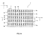
- FIGs. 1A and 1B are sectional views schematically showing the intensity of an electric field of propagation light in a one-dimensional photonic crystal 1.
- FIG. 1A shows a cross-section of the one-dimensional photonic crystal 1 schematically showing the intensity of the electric field of first band propagation light in the Z-axis direction.
- FIG. 1B shows a cross-section of the one-dimensional photonic crystal 1 schematically showing the intensity of the electric field of higher-order band propagation light in the Z-axis direction.
- the one-dimensional photonic crystal 1 is a periodic multilayered body including materials 5a and 5b that are layered alternately.
- Incident light 2 enters the one-dimensional photonic crystal 1 from the left side, and outgoing light 3 leaves the one-dimensional photonic crystal 1 from the right side.
- the photonic crystal 1 has a refractive index that is periodic in the Y-axis direction and uniform in the Z-axis direction, which is a propagation direction of the propagation light.
- the electric field of the light is depicted in the form of waves.
- wave crests 4a of the electric field are shown as solid lines, and wave troughs 4b of the electric field are shown as dashed lines.
- the size of the amplitude is expressed by the thickness of those lines, and a thicker line represents a larger amplitude.
- the wavelength of the propagation light is ⁇ .
- the wave crests 4a and the wave troughs 4b of the electric field form planes perpendicular to the Z axis, so that a propagation that is close to a plane wave is attained.
- nodes 4c at which the electric field amplitude becomes zero occur near the boundary of the material 5a and the material 5b, for example, as shown in FIG. 1B. Therefore, one period of the layered structure formed by the adjacent material 5a and material 5b is partitioned into two regions with a wave crest and a wave trough. Since the phases of the waves are shifted by half a wavelength at the adjacent regions (material 5a and material 5b), the wave crests and wave troughs appear alternately. It is in the second and the third band that these two nodes 4c per period occur. Although not shown in the figure, for the guided light in the higher-order bands, the number of nodes per period increases even more, and shifts by half a wavelength occur several times per period.
- FIG. 2 is a sectional view schematically showing the intensity of the electric field of the higher-order band propagation light in a waveguide element in which a phase grating is disposed on an incident side of the one-dimensional photonic crystal 1.
- a phase grating 6 is a phase modulation means for causing a difference of half a wavelength in the period b in the Y-axis direction.
- a plane wave 7 solid lines indicate wave crests of the electric field, dashed lines indicate wave troughs of the electric field, and the amplitude is expressed by the thickness of those lines
- an electric field pattern 8 that is similar to the higher-order band propagation light shown in FIG.
- phase modulation means behind an exit side end face 1b of the one-dimensional photonic crystal, thus restoring the higher-order band propagation light that has left the end face 1b into a plane wave.
- the technique combining the propagation in the bands on the boundary of the Brillouin zones and the phase modulation using the "one-dimensional photonic crystal having no periodicity in the propagation direction" described above is expanded to two-dimensional photonic crystal or photonic crystals with higher dimensions.
- FIG. 3 is a perspective view showing the structure of a two-dimensional photonic crystal 11 having a periodicity in the X-axis direction and the Y-axis direction and having no periodicity in the Z-axis direction.
- the two-dimensional photonic crystal 11 includes a plurality of cylindrical materials 15a arranged along the Z axis and a material 15b with a refractive index n B arranged between the materials 15a.
- the materials 15a have a radius R and a refractive index n A .
- the materials 15a are arranged in a square pattern with a period a.
- the photonic crystal 11 has a refractive index that is uniform in the Z-axis direction and has a refractive index structure that is periodic in the X-axis direction and the Y-axis direction.
- FIG. 3 when a plane wave with a vacuum wavelength of ⁇ 0 is allowed to enter from an end face 11a of the photonic crystal 11, how this light propagates within the photonic crystal 11 can be determined by calculating and plotting the photonic bands. It should be noted that the end face 11a is perpendicular to the Z axis. Methods of band calculation are described in detail in "Photonic Crystals", Princeton University Press (1995) and in Physical Review vol. B 44, No. 16, p. 8565, 1991, for example.
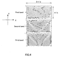
- FIG. 4 is a band diagram for the photonic crystal 11 in FIG. 3. The conditions in FIG. 4 are shown below. It is noted that the radius R is expressed by the period a of the photonic crystal 11.
- the band diagram is shown as contour lines by connecting the points with equal normalized frequencies ⁇ a/2 ⁇ c, and subscripts in the diagram denote the values of ⁇ a/2 ⁇ c.
- ⁇ is the angular frequency of the incident light
- a is the period of the structure
- c is the speed of light in a vacuum.
- the normalized frequency also can be expressed as a/ ⁇ 0 using the vacuum wavelength ⁇ 0 of the incident light and thus is expressed as a/ ⁇ 0 in the following.
- the width of the Brillouin zone in the X-axis direction and the Y-axis direction is 2 ⁇ /a.
- the TE polarized light refers to polarized light whose electric field direction is the X-axis direction. In the case of FIG. 3, it is clear from the symmetry that the band diagram of TM polarized light (whose magnetic field direction is the X-axis direction) would have the same shape as this band diagram.
- FIG. 5 is a band diagram schematically showing the shape of band surfaces 12 with equal normalized frequencies a/ ⁇ 0 in the Brillouin zone 13 of the photonic crystal 11 in FIG. 3. Since there is no periodicity in the Z-axis direction, the structure spreads infinitely without any Brillouin zone boundary.
- FIG. 6 is a schematic band diagram, taken on the YZ plane, including the incident light to the photonic crystal 11 shown in FIG. 3. More specifically, it is a schematic view illustrating on the band diagram the propagation in the case where the plane wave with a normalized frequency a/ ⁇ 0 is made to enter the end face 11a (parallel with the XY plane) of the photonic crystal 11 shown in FIG. 3 obliquely at an incident angle ⁇ . For simplification, the inclination of the incident light is limited within the YZ plane.
- an arrow 24 indicates the direction of the incident light
- an arrow 25 indicates the energy propagation direction of the propagation light in the second band
- an arrow 26 indicates the energy propagation direction of the propagation light in the first band.
- the energy travel direction is a normal direction of the band surface 12.
- FIG. 5 it can be seen that, in order to make the travel direction of the propagating electromagnetic wave energy parallel with the Z axis, it is necessary to use for propagation, for example, a point 12a on which the inclination of the band surface 12 becomes parallel with the XY plane.
- FIGs. 7 and 7B show the Brillouin zone in the photonic crystal 11 shown in FIG. 3.
- FIGs. 7A and 7B indicate the positions at which the inclination of the band surface 12 of the band diagram as shown in FIG. 5 is parallel with the XY plane.
- FIG. 7A is a plan view taken on the XY plane
- FIG. 7B is a perspective view. As shown in FIGs.
- the points on which the inclination of the band surface 12 of the band diagram as shown in FIG. 5 is parallel with the XY plane are located on each of lines A, B1, B2, B3, B4, C1, C2, C3 and C4 in the Brillouin zone owing to the symmetry.
- lines A, B1, B2, B3, B4, C1, C2, C3 and C4 in the Brillouin zone owing to the symmetry are located on each of lines A, B1, B2, B3, B4, C1, C2, C3 and C4 in the Brillouin zone owing to the symmetry.
- propagation by B1, B2, B3, B4, C1, C2, C3 and C4 on the Brillouin zone boundaries will be utilized.
- a wave vector k 1 of the incident plane wave corresponding to a point on the line B1 is as follows.
- k 1 (kx 1 , ky 1 , kz 1 )
- the vacuum wavelength ⁇ 0 of the plane wave can be calculated by the equation below.
- ⁇ 0 2 ⁇ n / (kx 1 2 + ky 1 2 + kz 1 2 ) 0.5
- the value of kz 1 needs to be set to large to an extent that the band corresponding to a/ ⁇ 0 is present on the line B1.
- the phase of the electromagnetic waves varies periodically in the XY plane, making it possible to achieve the propagation in the band on the Brillouin zone boundary. Similar effects can be obtained by inclining the incident end face 11a with respect to the XY plane, namely, by the configuration in which the incident end face 11a is not perpendicular to the propagation direction (Z-axis direction).
- the set of lines C1, C2, C3 and C4 in FIGs. 7A and 7B can be utilized similarly to the lines B1, B2, B3 and B4.
- the line A (which matches the Z axis) corresponds to the plane wave entering perpendicularly.
- the first band on the line A does not have sufficient characteristics of wavelength dispersion and group velocity anomaly.
- FIG. 8A is a perspective view showing a phase grating 16a generating diffraction waves in four directions according to the present embodiment.
- the phase grating 16a has a refractive index periodicity in plural directions (directions rotated by 45° from the X axis and the Y axis, respectively).
- phase grating 16a immediately after this phase grating 16a, it is possible to obtain the propagation light in the Z-axis direction on the lines B1, B2, B3 and B4.
- the phase grating 16a is desired to have a shape optimized so that desired diffraction light is intensified as much as possible.
- phase grating 16a optimized at a specific wavelength, even if the wavelength of the incident plane wave varies slightly, the efficiency of the first diffraction light does not drop sharply but remains at a high level, so that a wide wavelength range can be used. It is needless to say that, by optimizing the shape and period of the phase grating 16a, the wavefront corresponding to the set of lines C1, C2, C3 and C4 shown in FIGs. 7A and 7B can be achieved. More specifically, a phase grating 17a as shown in FIG. 8B is appropriate.
- FIG. 8B is a perspective view showing another phase grating 17a generating diffraction waves in four directions according to the present embodiment.
- the phase grating 17a has a refractive index periodicity in the X-axis direction and the Y-axis direction.
- a plane wave 70 is allowed to enter such a phase grating 17a perpendicularly (enter along the Z-axis direction)
- it is possible to generate by the interference of the diffraction light a diffraction wave 71 corresponding to the wave vector k 1 ', a diffraction wave 72 corresponding to the wave vector k 2 ', a diffraction wave 73 corresponding to the wave vector k 3 ' and a diffraction wave 74 corresponding to the wave vector k 4 '. Therefore, by providing the end face 11a of the photonic crystal 11 shown in FIG.
- the phase modulation also can be carried out by one or a combination of methods of "allowing a plane wave to enter obliquely the phase grating 16a or the phase grating 17a” and of “not providing the phase grating 16a or the phase grating 17a but processing the incident end face 11a of the photonic crystal 11 itself so as to have the same function as the phase grating 16a or the phase grating 17a.”
- phase modulation it is appropriate to dispose the above-noted phase grating 16a or the phase grating 17a shown in FIG. 8A or 8B as it is so that the positional relationship between its input end and output end is reversed, for example.
- the same phase grating is disposed symmetrically on both of the incident side and the exit side of the photonic crystal 11, the same effect is achieved for propagation light in both directions, so that optical fibers can be coupled as they are to both ends, for example.
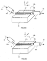
- FIG. 9A is a perspective view showing the configuration of a waveguide element 40 using the photonic crystal according to the present embodiment.
- FIG. 9B is a sectional view, taken on the XY plane, showing a waveguide portion 47 of the waveguide element 40.
- the waveguide portion 47 including a two-dimensional photonic crystal 41 is formed on an appropriate substrate 49.
- the photonic crystal 41 has a uniform refractive index in the Z direction, which is a light propagation direction, and a refractive index that is periodic in the X-axis direction and the Y-axis direction, which are perpendicular to the light propagation direction. More specifically, as shown in FIG. 9B, a photonic crystal 57a and a photonic crystal 57c are provided on upper and lower surfaces (end faces parallel with the XZ plane) of the photonic crystal 41. Further, photonic crystals 57b are formed on right and left surfaces (end faces parallel with the YZ plane) of the photonic crystal 41.
- These photonic crystals 57a, 57b and 57c are claddings in the waveguide portion 47, have a refractive index periodicity or a material that is different from the photonic crystal 41 serving as a core and function such that light is confined in the photonic crystal 41.
- the photonic crystal 41 through which light propagates has parts in which a material 45a and a material 45b are layered alternately in a periodic manner and parts in which a material 45c is provided.
- the photonic crystal 41 has layers in which the material 45c and the material 45a are layered alternately in a periodic manner and layers in which the material 45c and the material 45b are layered alternately in a periodic manner.
- the material 45a, the material 45b and the material 45c extend in the Z-axis direction.
- the material 45c is the air in the present embodiment.
- the photonic crystal 41 has a refractive index periodicity in the direction other than the light propagation direction. As shown in FIG. 9B, the period in the Y-axis direction of the photonic crystal 41 is ay, whereas the period in the X-axis direction thereof is ax.
- phase grating 46a and 46b serving as a phase modulation portion.
- an incident portion such as a rod lens 52a for allowing incident light 42 to enter the phase grating 46a is provided.
- This rod lens 52a focuses the incident light 42 on the end face of the phase grating 46a. In this manner, the light can be made to enter the phase grating 46a perpendicularly.
- the exit end side of the phase grating 46b is provided with a rod lens 52b serving as an exit means.
- the phase grating 46a is designed to have a structure, for example, capable of generating the diffraction wave corresponding to the wave vector k 1 , the diffraction wave corresponding to the wave vector k 2 , the diffraction wave corresponding to the wave vector k 3 and the diffraction wave corresponding to the wave vector k 4 .
- This achieves the propagation in the band on the Brillouin zone boundary in the photonic crystal 41.
- the phase grating 46a and the phase grating 46b that are disposed near the end faces of the photonic crystal 41 respectively may be in contact with the photonic crystal 41.
- the photonic crystal 41 may be formed as one piece with the phase grating 46a and the phase grating 46b. This allows easier production.
- the incident light 42 from an optical fiber is focused by the rod lens 52a serving as the incident portion and allowed to enter the phase grating 46a disposed at a beam waist position.
- the incident light 42 whose phase has been modulated by the phase grating 46a enters the photonic crystal 41 serving as a core of the waveguide portion 47 and turns into specific higher-order band propagation light.
- the propagation on the Brillouin zone boundary is achieved in the photonic crystal 41 so as to bring about "very large wavelength dispersion" and "group velocity anomaly.”
- the propagation light is converted into a plane wave again by the phase grating 46b disposed at the exit end face of the photonic crystal 41, and allowed to enter the rod lens 52b by which it turns into the outgoing light 43.
- the outgoing light 43 is coupled to the optical fiber or the like.
- the higher-order band propagation light has a group velocity that varies considerably according to the wavelength of the incident light. Consequently, the waveguide element 40 can be used as optical control elements such as an optical retardation element and a dispersion compensation element in optical communications.
- the propagation light with a slow group velocity increases a non-linear optical effect as described above, it is possible to provide an element with still larger non-linear optical effect by doping the photonic crystal 41 with microscopic particles of a substance having a non-linear optical effect. It is noted that the waveguide element 40 has the above-mentioned effect as long as it is coupled to a band near the Brillouin zone boundary.
- the material 45a and the material 45b are formed alternately in the Y-axis direction on the substrate 49, thus forming a periodic multilayer film.
- a stripe-patterned mask is put on the XZ plane of the multilayer film formed of the material 45a and the material 45b so that grooves whose depth direction corresponds to the Y-axis direction are formed by etching. By forming these grooves, the material 45c, which is the air, is provided.
- the configuration of the waveguide portion 47 can be varied by changing the material for the multilayer film layered in the Y-axis direction, the pattern of the film thickness and the patterns of the groove width and period, etc.
- FIGs. 10A and 10B show the Brillouin zone in the photonic crystal 41 shown in FIG. 9B.
- FIG. 10A is a plan view taken on the XY plane
- FIG. 10B is a perspective view.
- the Brillouin zone has a rectangular shape in the XY plane.
- the combination of the incident plane waves is that of plane waves corresponding to the lines B1, B2, B3 and B4.
- the wave vectors k 1 , k 2 , k 3 and k 4 of these plane waves are shown below.
- k 1 (kx 1 , ky 1 , kz 1 )
- ⁇ 0 2 ⁇ n / (kx 1 2 + ky 1 2 + kz 1 2 ) 0.5
- the wave vectors k 1 and k 2 in the case of plane waves corresponding to the lines Cx1 and Cx2 shown in FIGs. 10A and 10B are as follows.
- k 1 (kx 1 , ky 1 , kz 1 )
- kz 1 kz
- kz k 2 (kx 2 , ky 2 , kz 2 )
- the wave vectors k 1 and k 2 in the case of plane waves corresponding to the lines Cy1 and Cy2 are as follows.
- k 1 (kx 1 , ky 1 , kz 1 )
- k 2 (kx 2 , ky 2 , kz 2 )
- the calculation method of the value of kz is the same as that described above.
- the waveguide element 40 of the present embodiment it is essential to confine light in the X-axis direction and the Y-axis direction of the photonic crystal 41.
- n indicates a refractive index of a medium in contact with a lateral surface of the photonic crystal 41.
- the effective refractive index sometimes is smaller than 1. In such cases, the light confinement cannot be performed even if the outside medium is vacuum. Then, it becomes necessary to prevent the propagation light from escaping. In that case, the refractive index period or structure of each of the photonic crystals 57a, 57b and 57c provided around the photonic crystal 41 in FIG. 9B are made different from those of the photonic crystal 41, thereby confining the propagation light. In other words, the photonic crystal 41 serving as the core is surrounded by the photonic crystals 57a, 57b and 57c having a different period, making it possible to confine the propagation light in the photonic crystal 41.
- FIG. 11 is a schematic band diagram, taken on the YZ plane, showing adjacent photonic crystals with respect to a wavelength ⁇ 0 .
- the photonic crystals shown in FIG. 11 have a period c and a period d, respectively (d > c).
- a period c propagation light in the Z direction on the Brillouin zone boundary is propagated (in the first band).
- an arrow 500 indicates an energy direction of the propagation light.
- a band 501 for the wavelength ⁇ 0 also is shown in the figure.
- a region in which no band is present in the Z direction (a band gap 502) is generated, so that there is no band corresponding to the propagation inside the photonic crystal (with a period c).
- the propagation light of the photonic crystal (with a period c) is not coupled to the photonic crystal (with a period d). In other words, the confinement is achieved.
- the material and structure of the photonic crystals 57a, 57b and 57c for confinement may be different from those of the photonic crystal 41 for propagation, though it is desired to use the same material with different periods in view of the effort involved in fabricating the multilayer film.
- the two-dimensional photonic crystal 57a having a different period from the photonic crystal 41 is provided on the upper side of the two-dimensional photonic crystal 41.
- the two-dimensional photonic crystals 57b having a different width from the photonic crystal 41 are provided on the right and left sides of the two-dimensional photonic crystal 41.
- the one-dimensional photonic crystal 57c having a different period from the photonic crystal 41 is provided on the lower side of the two-dimensional photonic crystal 41.
- the waveguide element 40 shown in FIGs. 9A and 9B also may have a configuration in which the lateral surfaces of the photonic crystal 41 are in direct contact with a homogeneous material such as an air layer, without providing the photonic crystals 57a, 57b and 57c.
- FIG. 12 is a sectional view showing a configuration of the photonic crystal 41 provided with reflecting layers 51.
- the photonic crystal 41 shown in FIG. 9B is surrounded by the photonic crystals 57a, 57b and 57c.
- the reflecting layers 51 such as metal films may be formed around the photonic crystal 41 as shown in FIG. 12. In this manner, the propagation light can propagate in the photonic crystal 41 without leaking to the outside.
- FIG. 9C is a perspective view showing the configuration of a waveguide element 40a using another photonic crystal according to the present embodiment. Unlike the waveguide element 40 shown in FIG. 9A, the waveguide element 40a shown in FIG.
- 9C includes no phase grating 46a, and a rod lens 52a serving as the incident portion allows light to enter the incident end face not perpendicularly but at a certain angle (an incident angle ⁇ ).
- the incident end face is perpendicular to the Z axis.
- the rod lens 52a for allowing the inclined light to enter the incident end face serves as the phase modulation portion.
- the propagation in the band on the Brillouin zone boundary may be achieved in the photonic crystal 41 by inclining the incident end face of the photonic crystal with respect to the propagation direction so as to allow light to enter the incident end face obliquely.
- a waveguide element 40b shown in FIG. 9D is appropriate.
- FIG. 9D is a perspective view showing the configuration of the waveguide element 40b using another photonic crystal according to the present embodiment. Unlike the waveguide portion 47 of the waveguide element 40a shown in FIG. 9C, a waveguide portion 47a of the waveguide element 40b shown in FIG. 9D has an incident end face that is not perpendicular to the propagation direction of the propagation light (the Z direction).
- the waveguide element 40b shown in FIG. 9D is the same as the waveguide element shown in FIG. 9C.
- the incident end face of the waveguide portion 47a is inclined, and the incident end face of the photonic crystal serving as a core of the waveguide portion 47a also is not perpendicular to but inclined with respect to the propagation direction (the Z direction).
- the rod lens 52a is disposed such that the light enters at an incident angle ⁇ with respect to the incident end face.
- the present embodiment is not limited to this and has a similar effect even in the case of a so-called photonic crystal fiber in which the two-dimensional photonic crystal has a substantially circular cross-section and the photonic crystal itself has a cylindrical shape (a fiber shape).
- FIG. 13 is a perspective view showing the configuration of a basic two-dimensional photonic crystal optical fiber.
- a cylindrical optical fiber 130 has a core 131 with a two-dimensional periodic structure around its center axis and a cladding 132 with no periodicity that surrounds the core 131.
- FIG. 14A is a perspective view showing the structure of a waveguide element 145 using a fiber-shaped photonic crystal according to the present embodiment.
- An optical fiber 140 has a core 141 with a two-dimensional periodic structure and a cladding 142 that surrounds the core 141.
- phase gratings 146a and 146b are disposed.
- incident light which is a plane wave
- the light subjected to the phase modulation enters the core 141, propagates through the core 141 as higher-order band light and exits from the core 141.
- the light that has exited from the core 141 is diffraction light but is restored again to a plane wave by the phase grating 146b and then enters a rod lens 143b serving as the exit portion.
- the phase gratings 146a and 146b at both ends have the same shape and can be used in either of the incident and outgoing directions.
- the phase grating 146a is configured to phase-modulate the plane wave so that the propagation in the band on the Brillouin zone boundary is achieved in the photonic crystal 41 as described above.
- the waveguide element 145 Because of its fiber shape, the waveguide element 145 has a wide range of uses.
- the cladding 142 and the core 141 both are photonic crystals, they have different periods and structures so as to function to confine the propagation light in the core 141 by the photonic band gap.
- FIG. 14B is a perspective view showing the configuration of another optical fiber 150 that can be used for the waveguide element 145 in FIG. 14A.
- a core 151 of the optical fiber 150 has a configuration similar to that of the core 141 of the optical fiber 140 in FIG. 14A.
- a cladding 152 may have a concentric photonic crystal structure having a periodicity in a radial direction.
- Such a cladding structure can be produced by winding and then fixing two layers of thin films with different refractive indices, followed by spinning and drawing, as suggested in a document, Photonics West 2003 Technical summary digest, p. 383, lecture number C4993-04, for example.
- phase gratings 146a and 146b shown in FIG. 14A be disposed at the incident and exit ends of the optical fiber 150 shown in FIG. 14B.
- the plane wave is subjected to a phase modulation by the phase grating 146a and then coupled to the optical fiber 140 or the optical fiber 150, whereby a higher-order band propagates in the optical fiber 140 or the optical fiber 150.
- This brings about a group velocity anomaly much larger than that in the case of a conventional optical fiber using a single mode propagation in a lowest-order band. Consequently, large dispersion compensation effects and non-linear optical effects can be achieved.
- the core 141 and the core 151 have a periodic structure and do not have any limitation on their size, it is possible to provide a core with a large diameter easily, thus allowing a simple connection between fibers.
- the fiber-shaped photonic crystal can be obtained by forming a plurality of cavities along a longitudinal direction in a fiber-shaped homogeneous material, with the plurality of cavities being arranged to have symmetrical periodicities with respect to an axis parallel with the longitudinal direction. All or some of these cavities also can be filled with a fluid material, for example.
- FIG. 15A illustrates the arrangement of cavities in the core 141 in the XY plane of the optical fiber 140 shown in FIG. 14A.
- cavities 161 are formed in a homogeneous material 162.
- a period e is the distance between the cavities 161.
- FIGs. 15B and 15C show the Brillouin zone in the structure shown in FIG. 15A.
- FIG. 15B is a plan view taken on the XY plane
- FIG. 15C is a perspective view.
- the Brillouin zone in the XY plane is hexagonal.
- the combination of the incident plane waves may be a superposition of plane waves corresponding to lines B1, B2, B3, B4, B5 and B6 or that of plane waves corresponding to lines C1 to C6, for example.
- a so-called "photonic crystal group velocity anomaly” occurs in the light propagated in the higher-order propagation bands, so that an increased non-linear optical effect can be expected.
- no energy is taken up by the first band light in which there is substantially no group velocity anomaly. Therefore, it is possible to attain an increased effect of optical non-linearities by, for example, including non-linear optical material in the core of the multilayer film or the photonic crystal optical fiber (see Optical Fiber Communication 2002/Conference and Exhibit Technical Digest, ThK4, p. 468, for example).
- the material of the photonic crystal is not particularly limited as long as its transparency can be ensured in the wavelength range used.
- Suitable materials are silica, silicon, titanium oxide, tantalum oxide, niobium oxide, magnesium fluoride and silicon nitride, which are ordinarily used as the material for multilayer films and which have excellent durability and film-manufacturing costs. With these materials, a multilayer film can be formed easily by well-known methods such as sputtering, vacuum deposition, ion assisted deposition or plasma CVD.
- the waveguide element 40 shown in FIG. 9A may have a so-called airbridge structure, which uses no substrate 49.
- refractive index ratios that can be used in practice, when the air (with a refractive index of 1) is used as the low refractive index material and InSb (with a refractive index n of 4.21) is used as the high refractive index material, then a refractive index ratio equal to or greater than 4 can be attained (see "BISHOKOGAKU HANDBOOK" (Microoptics Handbook), Asakura Shoten, 1995, p. 224).
- the photonic crystal fiber can be produced by a generally known method of spinning quartz glass pipes that are bundled together.
- the refractive index periodic structure is formed by the combination of the quartz and the air holes, which brings about a sufficient effect.
- the waveguide element using the photonic crystal according to the present embodiment can achieve its effect in an optical element in a typically used wavelength range of about 200 nm to 20 ⁇ m.
- the principle of the photonic crystal is applicable to general electromagnetic waves, it also can be applied to electric waves with longer wavelengths and X-rays and gamma rays with shorter wavelengths.
- the waveguide element using the photonic crystal according to the present embodiment can be applied not only for light but also for electromagnetic waves in general.
- the refractive index periodicity in the propagation direction of the electromagnetic waves is not a necessary condition.
- a Bragg diffraction grating having a slight difference in refractive index in the propagation direction it also is possible to reflect only an electromagnetic wave at a specific wavelength, for example.
- an electromagnetic wave simulation (a finite element method) was conducted under the following conditions with respect to the case where a plane wave was allowed to enter the end face 11a of the two-dimensional photonic crystal 11 shown in FIG. 3.
- all the lengths were normalized with reference to the period a, which was a refractive index period.
- the materials 15a which were cylindrical cavities, were arranged in a square pattern.
- the photonic band diagram (TE polarized light) was the same as that shown in FIG. 4.
- k 1 (kx 1 , ky 1 , kz 1 )
- kz k 2 (kx 2 , ky 2 , kz 2 )
- kz k 3 (kx 3 , ky 3 , kz 3 )
- the result of the simulation of the propagation inside the photonic crystal by the finite element method is shown below.
- the software used here was JMAG manufactured by The Japan Research Institute, Limited.
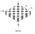
- FIG. 16 shows a calculation model in the simulation.
- FIG. 17 shows an electric field intensity distribution in the simulation in the calculation example.
- the calculation model expands infinitely in the X and Y directions.
- the calculation was carried out for one period of the incident plane wave as shown in FIG. 17. This was equivalent to an infinite periodic structure because a periodic boundary condition was set.
- FIG. 17 Black parts indicate a strong electric field, numeral 174 denotes a crest of the electric field, and numeral 173 denotes a trough of the electric field.
- numeral 174 denotes a crest of the electric field
- numeral 173 denotes a trough of the electric field.
- the electric field pattern shown in FIG. 17 will be described.
- a central cylinder is the crest of the electric field, and cylinders at four corners (shown partially in the figure) are troughs thereof.
- the electric field is localized in the cylindrical portions in the materials 15a and weakens in the portion of the material 15b.
- the adjacent cylinders have phases that are shifted by half a period, which indicates that the propagation in higher-order bands is present.
- FIG. 18 shows an electric field intensity distribution in the simulation in the comparative example.
- black parts indicate a strong electric field
- numeral 174 denotes a crest of the electric field
- numeral 173 denotes a trough of the electric field.
- the electric field intensity distribution obtained by the simulation shown in FIG. 18 showed that the electric field pattern was complicated and the propagations in a plurality of bands were superposed. Further, it was shown to be in phase in the XY plane.
- the waveguide element using the photonic crystal according to the present embodiment can be used as an optical waveguide element utilizing higher-order band propagation light in a photonic crystal.
- it is widely applicable as optical elements utilizing a dispersion compensation and an effect of increased optical non-linearity due to a group velocity anomaly of the higher-order band propagation light.
- the waveguide element using the photonic crystal according to the present embodiment is capable of controlling electromagnetic waves at all wavelengths, it can be used not only as an optical element but as an electromagnetic wave control element.
- a waveguide element using a photonic crystal according to the present invention can be used as an electromagnetic wave control element for a wide wavelength range.
Abstract
Description
Claims (19)
- A waveguide element using a photonic crystal, the waveguide element comprising:wherein an incident side phase modulation portion is provided for allowing an electromagnetic wave that is coupled to a band on or near a Brillouin zone boundary in a photonic band structure in the core and propagates in the core to enter the core.a core formed of a photonic crystal having a refractive index periodicity in at least two directions perpendicular to a propagation direction of an electromagnetic wave; anda cladding arranged in contact with the core in order to confine the electromagnetic wave in the core;
- The waveguide element using a photonic crystal according to claim 1, wherein the incident side phase modulation portion allows the electromagnetic wave that entirely or mostly belongs to a single photonic band and propagates in the core to enter the core.
- The waveguide element using a photonic crystal according to claim 1, wherein the photonic crystal serving as the core has no refractive index periodicity in the propagation direction of the electromagnetic wave.
- The waveguide element using a photonic crystal according to claim 1, wherein the incident side phase modulation portion allows a substantially plane wave having an inclination angle with respect to an incident surface of the core to enter the core.
- The waveguide element using a photonic crystal according to claim 1, wherein an incident surface of the core is inclined with respect to a plane perpendicular to the propagation direction of the electromagnetic wave, and the incident side phase modulation portion allows a substantially plane wave to enter the core.
- The waveguide element using a photonic crystal according to claim 1, wherein, at an incident surface of the core, the incident side phase modulation portion allows the electromagnetic wave subjected to a phase modulation periodically into an in-plane direction parallel with the incident surface to enter the core.
- The waveguide element using a photonic crystal according to claim 6, wherein the incident side phase modulation portion allows a plurality of substantially plane waves to enter the incident surface of the core and allows the plurality of substantially plane waves to interfere with each other at the incident surface, thereby allowing the electromagnetic wave subjected to the phase modulation to enter the core.
- The waveguide element using a photonic crystal according to claim 6, wherein the incident side phase modulation portion comprises
a phase grating disposed at a position close to or in contact with the incident surface of the core, and
an incident portion for allowing an electromagnetic wave to enter the phase grating. - The waveguide element using a photonic crystal according to claim 8, wherein the phase grating is formed as one piece with the core.
- The waveguide element using a photonic crystal according to claim 1, further comprising an exit side phase modulation portion disposed at a position close to or in contact with an exit surface of the core from which an electromagnetic wave exits,
wherein the exit side phase modulation portion converts the electromagnetic wave that exits from the core into a substantially plane wave. - The waveguide element using a photonic crystal according to claim 10, wherein the exit side phase modulation portion is formed as one piece with the core.
- The waveguide element using a photonic crystal according to claim 10, wherein the exit side phase modulation portion has an identical structure with the incident side phase modulation portion and is disposed such that a positional relationship between incident and exit ends of the exit side phase modulation portion is reversed from that of the incident side phase modulation portion.
- The waveguide element using a photonic crystal according to claim 1, wherein the cladding is a photonic crystal having a refractive index periodicity in at least one direction perpendicular to the propagation direction of the electromagnetic wave propagating in the core.
- The waveguide element according to claim 13, wherein the cladding is the photonic crystal having no refractive index periodicity in the propagation direction of the electromagnetic wave propagating in the core.
- The waveguide element using a photonic crystal according to claim 1, wherein a waveguide portion constituted by the core and the cladding has a structure in which a plurality of parallel grooves are formed in a multilayered body having a plurality of periods, and
the grooves are perpendicular to each layer in the multilayered body and run along the propagation direction of the electromagnetic wave. - The waveguide element using a photonic crystal according to claim 1, wherein the core is a homogeneous material in which a plurality of cavities extending along the propagation direction of the electromagnetic wave are formed, and
the cavities are arranged so as to have a constant period in a plane perpendicular to the propagation direction of the electromagnetic wave. - The waveguide element using a photonic crystal according to claim 16, wherein all or some of the plurality of cavities are filled with a fluid material.
- The waveguide element using a photonic crystal according to claim 16, wherein all or some of the plurality of cavities are filled with an active material having an optical non-linear effect.
- The waveguide element using a photonic crystal according to claim 16, wherein the core has a fiber shape with a substantially circular cross-section.
Applications Claiming Priority (3)
| Application Number | Priority Date | Filing Date | Title |
|---|---|---|---|
| JP2003056549 | 2003-03-04 | ||
| JP2003056549 | 2003-03-04 | ||
| PCT/JP2004/002749 WO2004081626A1 (en) | 2003-03-04 | 2004-03-04 | Waveguide device using photonic crystal |
Publications (2)
| Publication Number | Publication Date |
|---|---|
| EP1605285A1 true EP1605285A1 (en) | 2005-12-14 |
| EP1605285A4 EP1605285A4 (en) | 2006-06-14 |
Family
ID=32984376
Family Applications (1)
| Application Number | Title | Priority Date | Filing Date |
|---|---|---|---|
| EP04717257A Withdrawn EP1605285A4 (en) | 2003-03-04 | 2004-03-04 | Waveguide device using photonic crystal |
Country Status (5)
| Country | Link |
|---|---|
| US (1) | US7260300B2 (en) |
| EP (1) | EP1605285A4 (en) |
| JP (1) | JPWO2004081626A1 (en) |
| CN (1) | CN1756977A (en) |
| WO (1) | WO2004081626A1 (en) |
Families Citing this family (9)
| Publication number | Priority date | Publication date | Assignee | Title |
|---|---|---|---|---|
| EP1536252A4 (en) * | 2002-07-08 | 2005-11-02 | Nippon Sheet Glass Co Ltd | Photonic crystal optical waveguide |
| WO2006077765A1 (en) * | 2005-01-18 | 2006-07-27 | Nippon Sheet Glass Company, Limited | Waveguide device, method for fabricating waveguide device and optical sensor |
| JP2006337574A (en) * | 2005-05-31 | 2006-12-14 | Nippon Sheet Glass Co Ltd | Waveguide element |
| JP5019731B2 (en) * | 2005-09-06 | 2012-09-05 | 国立大学法人 東京大学 | Optical device |
| JP5864892B2 (en) * | 2010-06-02 | 2016-02-17 | キヤノン株式会社 | X-ray waveguide |
| JP5783785B2 (en) | 2010-06-02 | 2015-09-24 | キヤノン株式会社 | X-ray waveguide |
| JP2012226081A (en) * | 2011-04-19 | 2012-11-15 | Canon Inc | X-ray waveguide |
| JP6324843B2 (en) * | 2014-08-19 | 2018-05-16 | 日本電信電話株式会社 | Optical confinement structure |
| CN113646668A (en) * | 2019-04-11 | 2021-11-12 | 应用材料公司 | Multi-depth film for optical devices |
Citations (8)
| Publication number | Priority date | Publication date | Assignee | Title |
|---|---|---|---|---|
| EP1039561A2 (en) * | 1999-03-23 | 2000-09-27 | Seiko Epson Corporation | Light-emitting device |
| US6134043A (en) * | 1998-08-11 | 2000-10-17 | Massachusetts Institute Of Technology | Composite photonic crystals |
| JP2001051244A (en) * | 1999-08-11 | 2001-02-23 | Communication Research Laboratory Mpt | Optical modulator using photonic band gap structure and optical modulation method |
| EP1211531A2 (en) * | 2000-12-04 | 2002-06-05 | Nippon Sheet Glass Co., Ltd. | Optical device and spectroscopic, integrated optical apparatus using the optical device |
| EP1248123A2 (en) * | 2001-04-06 | 2002-10-09 | Nippon Sheet Glass Co., Ltd. | Photonic crystal for wavelength multiplexing |
| US20030142385A1 (en) * | 2002-01-22 | 2003-07-31 | Shigeo Kittaka | Optical element |
| WO2003079071A1 (en) * | 2002-03-15 | 2003-09-25 | Technical University Of Denmark | Planar optical waveguides with photonic crystal structure |
| US20030184845A1 (en) * | 2002-03-27 | 2003-10-02 | Shigeo Kittaka | Optical element using one-dimensional photonic crystal and optical device using the same |
Family Cites Families (8)
| Publication number | Priority date | Publication date | Assignee | Title |
|---|---|---|---|---|
| GB9710062D0 (en) * | 1997-05-16 | 1997-07-09 | British Tech Group | Optical devices and methods of fabrication thereof |
| WO1999042892A1 (en) * | 1998-02-19 | 1999-08-26 | Massachusetts Institute Of Technology | Photonic crystal omnidirectional reflector |
| JP2002236206A (en) | 2000-09-04 | 2002-08-23 | Nippon Sheet Glass Co Ltd | Optical device and spectroscopic apparatus using the same |
| US20020027655A1 (en) * | 2000-09-04 | 2002-03-07 | Shigeo Kittaka | Optical device and spectroscopic and polarization separating apparatus using the same |
| US6597721B1 (en) * | 2000-09-21 | 2003-07-22 | Ut-Battelle, Llc | Micro-laser |
| DE60235781D1 (en) * | 2001-02-09 | 2010-05-12 | Panasonic Corp | Optical device |
| JP2002303836A (en) * | 2001-04-04 | 2002-10-18 | Nec Corp | Optical switch with photonic crystal structure |
| JP4132963B2 (en) * | 2002-05-17 | 2008-08-13 | 日本板硝子株式会社 | Optical element using one-dimensional photonic crystal and spectroscopic device using the same |
-
2004
- 2004-03-04 JP JP2005503495A patent/JPWO2004081626A1/en active Pending
- 2004-03-04 WO PCT/JP2004/002749 patent/WO2004081626A1/en not_active Application Discontinuation
- 2004-03-04 CN CN200480005901.4A patent/CN1756977A/en active Pending
- 2004-03-04 EP EP04717257A patent/EP1605285A4/en not_active Withdrawn
- 2004-03-04 US US10/547,535 patent/US7260300B2/en not_active Expired - Fee Related
Patent Citations (8)
| Publication number | Priority date | Publication date | Assignee | Title |
|---|---|---|---|---|
| US6134043A (en) * | 1998-08-11 | 2000-10-17 | Massachusetts Institute Of Technology | Composite photonic crystals |
| EP1039561A2 (en) * | 1999-03-23 | 2000-09-27 | Seiko Epson Corporation | Light-emitting device |
| JP2001051244A (en) * | 1999-08-11 | 2001-02-23 | Communication Research Laboratory Mpt | Optical modulator using photonic band gap structure and optical modulation method |
| EP1211531A2 (en) * | 2000-12-04 | 2002-06-05 | Nippon Sheet Glass Co., Ltd. | Optical device and spectroscopic, integrated optical apparatus using the optical device |
| EP1248123A2 (en) * | 2001-04-06 | 2002-10-09 | Nippon Sheet Glass Co., Ltd. | Photonic crystal for wavelength multiplexing |
| US20030142385A1 (en) * | 2002-01-22 | 2003-07-31 | Shigeo Kittaka | Optical element |
| WO2003079071A1 (en) * | 2002-03-15 | 2003-09-25 | Technical University Of Denmark | Planar optical waveguides with photonic crystal structure |
| US20030184845A1 (en) * | 2002-03-27 | 2003-10-02 | Shigeo Kittaka | Optical element using one-dimensional photonic crystal and optical device using the same |
Non-Patent Citations (2)
| Title |
|---|
| PATENT ABSTRACTS OF JAPAN vol. 2000, no. 19, 5 June 2001 (2001-06-05) -& JP 2001 051244 A (COMMUNICATION RESEARCH LABORATORY MPT), 23 February 2001 (2001-02-23) * |
| See also references of WO2004081626A1 * |
Also Published As
| Publication number | Publication date |
|---|---|
| CN1756977A (en) | 2006-04-05 |
| US20060078263A1 (en) | 2006-04-13 |
| JPWO2004081626A1 (en) | 2006-06-15 |
| EP1605285A4 (en) | 2006-06-14 |
| US7260300B2 (en) | 2007-08-21 |
| WO2004081626A1 (en) | 2004-09-23 |
Similar Documents
| Publication | Publication Date | Title |
|---|---|---|
| US7046887B2 (en) | Polarization preserving optical fiber and absolute single polarization optical fiber | |
| Hu et al. | Realization of ultrathin waveguides by elastic metagratings | |
| WO2005022221A1 (en) | Electromagnetic wave frequency filter | |
| JP4132963B2 (en) | Optical element using one-dimensional photonic crystal and spectroscopic device using the same | |
| WO2012002222A1 (en) | Design for achieving low loss in intersecting region of optical waveguide | |
| JP4900572B2 (en) | 2D photonic crystal | |
| US7260300B2 (en) | Waveguide element using photonic crystal | |
| EP1536252A1 (en) | Photonic crystal optical waveguide | |
| US20070058915A1 (en) | Waveguide element using photonic crystal | |
| JP3766844B2 (en) | Lattice modulation photonic crystal | |
| JP2012013679A (en) | X-ray waveguide | |
| Silvestre et al. | Analysis and design of an endlessly single-mode finned dielectric waveguide | |
| JP4078527B2 (en) | Structure of antireflection film on one-dimensional photonic crystal and method for forming the same | |
| GB2386966A (en) | Optical element using one-dimensional photonic crystal and phase modulation unit | |
| US7305155B2 (en) | Optical element and wavelength separator using the same | |
| JP2713358B2 (en) | Wavelength selective filter for pillbox type optical resonator | |
| Fan et al. | Manipulating light with photonic crystals | |
| US7224868B2 (en) | Radiation-free optical cavity | |
| JP2003131028A (en) | Optical circuit | |
| JPWO2006103850A1 (en) | Waveguide element and laser generator | |
| JP4956741B2 (en) | Photonic crystal waveguide | |
| KR20030026364A (en) | Optical waveguide diffraction grating device and its fabrication method | |
| JP2007304629A (en) | Structure of anti-reflection film on two or three dimensional photonic crystal and method of forming same | |
| JP2001201649A (en) | Coaxial periodic structure optical waveguide and optical filter using same | |
| Joannopoulos et al. | Novelties of light with photonic crystals |
Legal Events
| Date | Code | Title | Description |
|---|---|---|---|
| PUAI | Public reference made under article 153(3) epc to a published international application that has entered the european phase |
Free format text: ORIGINAL CODE: 0009012 |
|
| 17P | Request for examination filed |
Effective date: 20050921 |
|
| AK | Designated contracting states |
Kind code of ref document: A1 Designated state(s): AT BE BG CH CY CZ DE DK EE ES FI FR GB GR HU IE IT LI LU MC NL PL PT RO SE SI SK TR |
|
| AX | Request for extension of the european patent |
Extension state: AL LT LV MK |
|
| RIN1 | Information on inventor provided before grant (corrected) |
Inventor name: ASAI, TAKAHIRO C/O NIPPON SHEET GLASS COMP., LTD. Inventor name: TSUNETOMO, KEIJI C/O NIPPON SHEET GLASS COMP.,LTD. Inventor name: NARA, MASATOSHI C/O NIPPON SHEET GLASS COMP., LTD. Inventor name: OYA, KAZUAKI C/O NIPPON SHEET GLASS COMP., LTD. Inventor name: KITTAKA, SHIGEO C/O NIPPON SHEET GLASS COMP., LTD. |
|
| A4 | Supplementary search report drawn up and despatched |
Effective date: 20060427 |
|
| DAX | Request for extension of the european patent (deleted) | ||
| RBV | Designated contracting states (corrected) |
Designated state(s): DE FR GB |
|
| 17Q | First examination report despatched |
Effective date: 20070626 |
|
| STAA | Information on the status of an ep patent application or granted ep patent |
Free format text: STATUS: THE APPLICATION IS DEEMED TO BE WITHDRAWN |
|
| 18D | Application deemed to be withdrawn |
Effective date: 20071002 |