EP1610389A2 - Thin film transistor array substrate, display using the same, and fabrication method thereof - Google Patents
Thin film transistor array substrate, display using the same, and fabrication method thereof Download PDFInfo
- Publication number
- EP1610389A2 EP1610389A2 EP05105583A EP05105583A EP1610389A2 EP 1610389 A2 EP1610389 A2 EP 1610389A2 EP 05105583 A EP05105583 A EP 05105583A EP 05105583 A EP05105583 A EP 05105583A EP 1610389 A2 EP1610389 A2 EP 1610389A2
- Authority
- EP
- European Patent Office
- Prior art keywords
- display
- pad
- insulating layer
- substrate
- coupled
- Prior art date
- Legal status (The legal status is an assumption and is not a legal conclusion. Google has not performed a legal analysis and makes no representation as to the accuracy of the status listed.)
- Granted
Links
- 239000000758 substrate Substances 0.000 title claims abstract description 75
- 238000000034 method Methods 0.000 title claims description 35
- 239000010409 thin film Substances 0.000 title claims description 26
- 238000004519 manufacturing process Methods 0.000 title abstract description 14
- 238000012360 testing method Methods 0.000 claims abstract description 96
- 239000000463 material Substances 0.000 claims description 4
- 239000010410 layer Substances 0.000 description 87
- 230000008569 process Effects 0.000 description 20
- 239000000523 sample Substances 0.000 description 13
- VYPSYNLAJGMNEJ-UHFFFAOYSA-N silicon dioxide Inorganic materials O=[Si]=O VYPSYNLAJGMNEJ-UHFFFAOYSA-N 0.000 description 11
- 229910052814 silicon oxide Inorganic materials 0.000 description 10
- 239000010408 film Substances 0.000 description 8
- 238000002347 injection Methods 0.000 description 8
- 239000007924 injection Substances 0.000 description 8
- 230000007547 defect Effects 0.000 description 6
- 230000005525 hole transport Effects 0.000 description 6
- 238000002161 passivation Methods 0.000 description 6
- 238000006748 scratching Methods 0.000 description 6
- 230000002393 scratching effect Effects 0.000 description 6
- 229910052581 Si3N4 Inorganic materials 0.000 description 5
- 239000003990 capacitor Substances 0.000 description 5
- HQVNEWCFYHHQES-UHFFFAOYSA-N silicon nitride Chemical compound N12[Si]34N5[Si]62N3[Si]51N64 HQVNEWCFYHHQES-UHFFFAOYSA-N 0.000 description 5
- 239000012212 insulator Substances 0.000 description 4
- 239000002356 single layer Substances 0.000 description 3
- 229910021417 amorphous silicon Inorganic materials 0.000 description 2
- 230000007797 corrosion Effects 0.000 description 2
- 238000005260 corrosion Methods 0.000 description 2
- 238000010586 diagram Methods 0.000 description 2
- 239000011521 glass Substances 0.000 description 2
- 150000002500 ions Chemical class 0.000 description 2
- 239000004973 liquid crystal related substance Substances 0.000 description 2
- 239000002184 metal Substances 0.000 description 2
- 238000012986 modification Methods 0.000 description 2
- 230000004048 modification Effects 0.000 description 2
- 239000012811 non-conductive material Substances 0.000 description 2
- 239000011368 organic material Substances 0.000 description 2
- 230000003252 repetitive effect Effects 0.000 description 2
- 230000004044 response Effects 0.000 description 2
- 239000004642 Polyimide Substances 0.000 description 1
- -1 acryl Chemical group 0.000 description 1
- 230000008901 benefit Effects 0.000 description 1
- 230000008878 coupling Effects 0.000 description 1
- 238000010168 coupling process Methods 0.000 description 1
- 238000005859 coupling reaction Methods 0.000 description 1
- 238000000206 photolithography Methods 0.000 description 1
- 229910021420 polycrystalline silicon Inorganic materials 0.000 description 1
- 229920005591 polysilicon Polymers 0.000 description 1
- 239000010453 quartz Substances 0.000 description 1
Images


Classifications
-
- G—PHYSICS
- G02—OPTICS
- G02F—OPTICAL DEVICES OR ARRANGEMENTS FOR THE CONTROL OF LIGHT BY MODIFICATION OF THE OPTICAL PROPERTIES OF THE MEDIA OF THE ELEMENTS INVOLVED THEREIN; NON-LINEAR OPTICS; FREQUENCY-CHANGING OF LIGHT; OPTICAL LOGIC ELEMENTS; OPTICAL ANALOGUE/DIGITAL CONVERTERS
- G02F1/00—Devices or arrangements for the control of the intensity, colour, phase, polarisation or direction of light arriving from an independent light source, e.g. switching, gating or modulating; Non-linear optics
- G02F1/01—Devices or arrangements for the control of the intensity, colour, phase, polarisation or direction of light arriving from an independent light source, e.g. switching, gating or modulating; Non-linear optics for the control of the intensity, phase, polarisation or colour
- G02F1/13—Devices or arrangements for the control of the intensity, colour, phase, polarisation or direction of light arriving from an independent light source, e.g. switching, gating or modulating; Non-linear optics for the control of the intensity, phase, polarisation or colour based on liquid crystals, e.g. single liquid crystal display cells
- G02F1/133—Constructional arrangements; Operation of liquid crystal cells; Circuit arrangements
- G02F1/1333—Constructional arrangements; Manufacturing methods
- G02F1/1345—Conductors connecting electrodes to cell terminals
- G02F1/13458—Terminal pads
-
- H—ELECTRICITY
- H01—ELECTRIC ELEMENTS
- H01L—SEMICONDUCTOR DEVICES NOT COVERED BY CLASS H10
- H01L27/00—Devices consisting of a plurality of semiconductor or other solid-state components formed in or on a common substrate
- H01L27/02—Devices consisting of a plurality of semiconductor or other solid-state components formed in or on a common substrate including semiconductor components specially adapted for rectifying, oscillating, amplifying or switching and having at least one potential-jump barrier or surface barrier; including integrated passive circuit elements with at least one potential-jump barrier or surface barrier
- H01L27/12—Devices consisting of a plurality of semiconductor or other solid-state components formed in or on a common substrate including semiconductor components specially adapted for rectifying, oscillating, amplifying or switching and having at least one potential-jump barrier or surface barrier; including integrated passive circuit elements with at least one potential-jump barrier or surface barrier the substrate being other than a semiconductor body, e.g. an insulating body
-
- H—ELECTRICITY
- H01—ELECTRIC ELEMENTS
- H01L—SEMICONDUCTOR DEVICES NOT COVERED BY CLASS H10
- H01L27/00—Devices consisting of a plurality of semiconductor or other solid-state components formed in or on a common substrate
- H01L27/15—Devices consisting of a plurality of semiconductor or other solid-state components formed in or on a common substrate including semiconductor components with at least one potential-jump barrier or surface barrier specially adapted for light emission
- H01L27/153—Devices consisting of a plurality of semiconductor or other solid-state components formed in or on a common substrate including semiconductor components with at least one potential-jump barrier or surface barrier specially adapted for light emission in a repetitive configuration, e.g. LED bars
- H01L27/156—Devices consisting of a plurality of semiconductor or other solid-state components formed in or on a common substrate including semiconductor components with at least one potential-jump barrier or surface barrier specially adapted for light emission in a repetitive configuration, e.g. LED bars two-dimensional arrays
-
- H—ELECTRICITY
- H10—SEMICONDUCTOR DEVICES; ELECTRIC SOLID-STATE DEVICES NOT OTHERWISE PROVIDED FOR
- H10K—ORGANIC ELECTRIC SOLID-STATE DEVICES
- H10K50/00—Organic light-emitting devices
- H10K50/80—Constructional details
- H10K50/84—Passivation; Containers; Encapsulations
- H10K50/844—Encapsulations
-
- H—ELECTRICITY
- H10—SEMICONDUCTOR DEVICES; ELECTRIC SOLID-STATE DEVICES NOT OTHERWISE PROVIDED FOR
- H10K—ORGANIC ELECTRIC SOLID-STATE DEVICES
- H10K59/00—Integrated devices, or assemblies of multiple devices, comprising at least one organic light-emitting element covered by group H10K50/00
- H10K59/10—OLED displays
- H10K59/12—Active-matrix OLED [AMOLED] displays
-
- H—ELECTRICITY
- H10—SEMICONDUCTOR DEVICES; ELECTRIC SOLID-STATE DEVICES NOT OTHERWISE PROVIDED FOR
- H10K—ORGANIC ELECTRIC SOLID-STATE DEVICES
- H10K59/00—Integrated devices, or assemblies of multiple devices, comprising at least one organic light-emitting element covered by group H10K50/00
- H10K59/80—Constructional details
- H10K59/88—Dummy elements, i.e. elements having non-functional features
-
- H—ELECTRICITY
- H10—SEMICONDUCTOR DEVICES; ELECTRIC SOLID-STATE DEVICES NOT OTHERWISE PROVIDED FOR
- H10K—ORGANIC ELECTRIC SOLID-STATE DEVICES
- H10K71/00—Manufacture or treatment specially adapted for the organic devices covered by this subclass
- H10K71/70—Testing, e.g. accelerated lifetime tests
-
- G—PHYSICS
- G02—OPTICS
- G02F—OPTICAL DEVICES OR ARRANGEMENTS FOR THE CONTROL OF LIGHT BY MODIFICATION OF THE OPTICAL PROPERTIES OF THE MEDIA OF THE ELEMENTS INVOLVED THEREIN; NON-LINEAR OPTICS; FREQUENCY-CHANGING OF LIGHT; OPTICAL LOGIC ELEMENTS; OPTICAL ANALOGUE/DIGITAL CONVERTERS
- G02F1/00—Devices or arrangements for the control of the intensity, colour, phase, polarisation or direction of light arriving from an independent light source, e.g. switching, gating or modulating; Non-linear optics
- G02F1/01—Devices or arrangements for the control of the intensity, colour, phase, polarisation or direction of light arriving from an independent light source, e.g. switching, gating or modulating; Non-linear optics for the control of the intensity, phase, polarisation or colour
- G02F1/13—Devices or arrangements for the control of the intensity, colour, phase, polarisation or direction of light arriving from an independent light source, e.g. switching, gating or modulating; Non-linear optics for the control of the intensity, phase, polarisation or colour based on liquid crystals, e.g. single liquid crystal display cells
- G02F1/133—Constructional arrangements; Operation of liquid crystal cells; Circuit arrangements
- G02F1/136—Liquid crystal cells structurally associated with a semi-conducting layer or substrate, e.g. cells forming part of an integrated circuit
- G02F1/1362—Active matrix addressed cells
- G02F1/136254—Checking; Testing
-
- H—ELECTRICITY
- H10—SEMICONDUCTOR DEVICES; ELECTRIC SOLID-STATE DEVICES NOT OTHERWISE PROVIDED FOR
- H10K—ORGANIC ELECTRIC SOLID-STATE DEVICES
- H10K59/00—Integrated devices, or assemblies of multiple devices, comprising at least one organic light-emitting element covered by group H10K50/00
- H10K59/10—OLED displays
- H10K59/12—Active-matrix OLED [AMOLED] displays
- H10K59/122—Pixel-defining structures or layers, e.g. banks
-
- H—ELECTRICITY
- H10—SEMICONDUCTOR DEVICES; ELECTRIC SOLID-STATE DEVICES NOT OTHERWISE PROVIDED FOR
- H10K—ORGANIC ELECTRIC SOLID-STATE DEVICES
- H10K59/00—Integrated devices, or assemblies of multiple devices, comprising at least one organic light-emitting element covered by group H10K50/00
- H10K59/10—OLED displays
- H10K59/12—Active-matrix OLED [AMOLED] displays
- H10K59/131—Interconnections, e.g. wiring lines or terminals
Definitions
- the present invention relates to a thin film transistor array substrate and a display using the same, and more particularly, to a thin film transistor array substrate having a testing pad for testing electrical characteristics of a thin film transistor, a display using the same, and a method of fabricating the same.
- a TFT is provided in a pixel and used for switch-controlling a pixel electrode.
- the TFT is made of a high or a low temperature poly silicon, amorphous silicon and is formed on an insulating substrate, such as a glass substrate or quartz substrate.
- a substrate referred to as a TFT substrate, includes a circuit having the TFT that is provided in an image displaying region and/or a region neighboring the image displaying region.
- the testing process for the TFT substrate is performed using an array tester for testing operations of an adjacent circuit.
- the array tester is classified as an e-beam type, a capacitor coupling type, or a direct contact type.
- the corresponding TFT is electrically tested by transmitting an electrical signal to the pad 6 through a testing probe directly contacting a pad 6 and then reading the electric signal again through the testing probe.
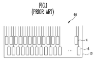
- the pad 6 is formed on one side of the TFT substrate 10 and connected to the TFT (not shown) through a signal line 4, as shown in FIG. 1.
- the direct contact type array tester is applicable for a high-resolution display having small-sized pixels.
- the present invention provides a thin film transistor array substrate including a testing pad for testing electrical characteristics of the thin film transistor, and an electroluminescent display using the same.
- the present invention discloses a display including a substrate having an image displaying part comprising a plurality of pixels, a dummy testing pad, and a first insulating layer covering the dummy testing pad.
- the present invention also discloses a thin film transistor array substrate including a thin film transistor array provided on the thin film transistor array substrate, a dummy testing pad, and a first insulating layer covering the dummy pad part, wherein the thin film transistor array comprises a plurality of data lines, a plurality of scan lines, and a thin film transistor coupled with the data lines and the scan lines.
- the present invention also discloses a method of forming a display, including forming a plurality of pixels on a substrate, forming a dummy testing pad coupled with at least one of the pixels, performing a test using the dummy testing pad, covering the dummy testing pad with a first insulating layer, and forming a light emitting device coupled with the pixel circuit.
- FIG. 1 shows a pad part formed on a conventional thin film transistor array substrate.
- FIG. 2 shows a light emitting display including a thin film transistor array substrate according to an embodiment of the invention.
- FIG. 3 is a circuit diagram of a pixel associated with the pixel of FIG. 2.
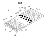
- FIG. 4 is a perspective view of a chip arrangement part associated with the chip arrangement part of FIG. 2.
- FIG. 5 is a sectional view of the chip arrangement part, taken along line I-I' of FIG. 4.
- FIG. 6 illustrates a light emitting display comprising a thin film transistor array substrate according to an embodiment of the invention.
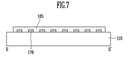
- FIG. 7 is a sectional view, taken along line II-II' of FIG. 6.
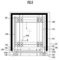
- FIG. 8 illustrates a light emitting display including a thin film transistor array substrate according to an embodiment of the invention.
- FIGs. 9A, 9B, 9C, and 9D are sectional views illustrating a method of fabricating a thin film transistor and a testing pad of each pixel shown in FIGs. 2, 6 and 8.
- FIG. 2 illustrates a light emitting display including a thin film transistor array substrate according to an embodiment of the invention.
- FIG. 3 is a circuit diagram of a pixel associated with a pixel of an image display part in FIG. 2.
- a light emitting display having a TFT array substrate includes an image display part 112 formed on a substrate 110, a dummy pad part 178, and an insulating layer (not shown).
- the light emitting display with the TFT array substrate may further include a scan driver 120, a data driver 130, a first power line 140, a second power line 142, and a pad part 150.
- the pad part 150 includes at least one TFT, a plurality of pixels 121 defined by a plurality of data lines D, a plurality of scan lines S, and a plurality of pixel power line VDD.
- Each pixel 121 includes a light emitting device LED and a pixel circuit 125. Each pixel 121 is selected according to a scan signal that is applied to the scan line S and emits light according to the data signal that is applied to the data line D.
- the light emitting device includes an anode electrode connected with the pixel circuit 125 and a cathode electrode that is connected with the second power line 142.
- the light emitting device LED may include an organic light emitting device.
- the organic light emitting device includes an emitting layer, an electron transport layer, and a hole transport layer, which are provided between an anode electrode and a cathode electrode.
- the light emitting display may further include an electron injection layer and a hole injection layer.
- electrons generated from the cathode electrode travel to the emitting layer via the electron injection layer and the electron transport layer, and holes generated from the anode electrode are moved to the emitting layer via the hole injection layer and the hole transport layer.
- the electrons from the electron transport layer and the holes from the hole transport layer are then recombined in the emitting layer, thereby emitting light.
- the pixel circuit 125 is provided with a first TFT M1, a second TFT M2, and a capacitor C.
- the first TFT M1 includes a gate electrode that is connected with the scan line S, a source electrode that is connected with the data line, and a drain electrode that is connected with the first node N1.
- the first TFT M1 transmits the data signal to the first node N1 in response to the scan signal transmitted to the scan line S.
- the second TFT M2 includes a gate electrode that is connected with the first node N1, which is connected with the drain electrode of the first TFT M1 and the capacitor C, a source electrode that is connected with a pixel power line VDD, and a drain electrode that is connected with the anode electrode of the LED.
- the second TFT M2 adjusts current that is applied from the pixel power line VDD to the LED according to the voltage that is applied to the gate electrode of the second TFT M2 that is connected with the first node N1, thereby allowing the LED to emit light.
- the capacitor C stores the voltage corresponding to the data signal applied to the first node N1 via the first TFT M1 while the scan signal is transmitted to the scan line S, and stores the second TFT M2 being turned on for one frame when the first TFT M1 is turned off.
- the display having the TFT array substrate may includes at least two TFTs and at least one capacitor for each pixel circuit 125 of each pixel 121.
- the dummy pad part 178 is connected with the plurality of data lines D and a testing pad 176 is only used for testing electrical characteristics of the TFT on the image displaying part 112 in a TFT array testing process.
- the pad part 150 is formed with a plurality of pads 152. Each of the plurality of pads may be arranged at a regular interval.
- the pad part 150 may be coupled with pads of a flexible printed circuit (FPC) (not shown), wherein the FPC may be flexible.
- the pads 152 of the pad part 150 when coupled with the FPC, receive a scan control signal for controlling the scan driver 120, a data control signal for controlling the data driver 130, and the data signal transmitted to the data driver 130 via the FPC.
- the pads 152 of the pad part 150 receive the first power from the first power line 140 and the second power from the second power line 142 via the FPC.
- the first power line 140 has opposite ends connected with at least one of the pads 152 of the pad part 150 through first power connection lines 144a and 144b.
- the first power line 140 supplies the first power from the pad part 150 to the pixel power line VDD of each pixel 121 on the image displaying part 112.
- the second power line 142 has one end connected with at least one of the pads 152 of the pad part 150 through a second power connection line 146.
- the second power line 142 may cover or be formed on the surface of the substrate 110 and is coupled with each pixel 121. Further, the second power line 142 may supply the second power from the pad part 150 to each pixel 121 of the image display part 112.
- the scan driver 120 generates the scan signal for driving the plurality of scan lines S in sequence in response to the scan control signal input through at least one signal line 135 from among the plurality of pads 152.
- the scan driver 120 may include a plurality of shift registers to generate the scan signal in sequence according to the scan control signal.
- the data driver 130 may be provided between the image displaying part 112 and the pad part 150 of the substrate 110.
- the data driver 130 transmits the data signal to the plurality of data lines D according to a data control signal that is transmitted from the plurality of pads 152 of the pad part 150.
- the data driver 130 may be mounted on a chip arrangement part by various methods, such as a chip-on-glass method, a wire-bonding method, a flip chip method, or a beam lead method.
- the chip arrangement part may be connected with the data line D through the plurality of first signal lines 134 and may be connected with the pads 152, to which the data signal and the data control signal are transmitted, through a plurality of second signal lines 132.
- FIG. 4 is a perspective view of a chip arrangement part associated with the chip arrangement part A of FIG. 2.
- the chip arrangement part 180 includes a first chip terminal 138 having first terminals 136 coupled with first output pins (not shown) of the data driver 130.
- the chip arrangement part 180 further includes a second chip terminal 188 having second terminals 186 coupled with second input pins (not shown) of the data driver 130. Further, the chip arrangement part 180 is formed with the dummy pad part 178. It is understood that the operation of the first chip terminal 138 having the first terminals 136 may be switched with the operation of the second chip terminal 188 having the second terminals 186.
- the first chip terminal 138 includes the first signal lines 134 connected with the data lines D, and the first terminals 136 formed in a predetermined pattern, such as, for example, arranged in a zigzag pattern, at each end of the first signal lines 134.
- the first chip terminal 138 supplies an output signal, i.e., the data signal of the data driver 130, to the data lines D.
- the second chip terminal 188 includes the second signal lines 132 connected with the plurality of pads 152 of the pad part150, and the second terminals 186 formed in a predetermined pattern, such as, for example, arranged in a zigzag pattern, at each end of the second signal lines 132.
- the second chip terminal 188 supplies the first input pins with the data control signal and the data signal from the flexible printed circuit via the pad part 150.
- the data driver 130 is provided on the first terminals 136 and the second terminals 186 of the chip arrangement part 180 after the TFT array testing process.
- the data driver 130 may be mounted thereon or integrally formed thereon.
- the dummy pad part 178 includes dummy signal lines 174 extending from the first terminals 136 of the first chip terminal 138, and a plurality of testing pads 176 formed in a predetermined pattern, such as, for example, arranged in a zigzag pattern, at each end of the dummy signal lines 174.
- a testing probe contacts the plurality of testing pads 176 during the TFT array testing process; therefore, the dummy pad part 178 is used to receive a testing signal from the testing probe so that the testing probe does not contact another portion of the substrate.
- a TFT array tester (not shown) contacts the pad part 150, thereby transmitting the scan control signal to the scan driver 120.
- the testing probe contacts the testing pad 176 of the dummy pad part 178 and transmits a testing signal to the testing pad 176 to determine whether the TFTs formed in each pixel 121 of the image displaying part 112 are operating properly.
- an insulating film is formed over the dummy pad part 178 of the substrate 110, preferably covering the dummy pad part 178.
- FIG. 5 is a sectional view of the chip arrangement part, taken along line I-I' of FIG. 4.
- a first insulating film 185 is formed over the dummy pad part 178 of the substrate 110, preferably covering the dummy pad part 178.
- the first insulating film 185 covers the testing pad 176 to prevent the exposure of any scratching of the testing pad 176, thereby preventing defects resulting from the scratching after the TFT array testing process is finished.
- At least one insulating film may be formed between the substrate 110 and the testing pad 176.
- an insulating layer and a passivation layer may be formed on the TFT of the image display part 112 on the substrate 110, and then a source/drain metal layer of the TFT and the testing pad 176 are formed thereon.
- the scan control signal may be initially transmitted to the scan driver 120 when the array tester (not shown) contacts the pad part 150 of the substrate 110.
- the testing signal is transmitted to the testing pad 176 by contacting the testing probe with the testing pad 176 of the dummy pad part 178 to determine whether each TFT formed on the substrate 110 operates properly according to the testing signal.
- the first insulating film 185 may be formed over the dummy pad part 178 of the substrate 110 after the electrical characteristics of the TFTs for the pixel and the scan driver 120are tested.
- the first insulating film 185 preferably covers the dummy pad part 178.
- TFT array substrate may be applied to a flat panel display, such as an LCD, an FED, a PDP, OLED, or a light emitting display.
- a flat panel display such as an LCD, an FED, a PDP, OLED, or a light emitting display.
- FIG. 6 shows an organic light emitting display (OLED) including a thin film transistor array substrate according to an embodiment of the invention.
- FIG. 7 is a sectional view, taken along line II-II' of FIG. 6.
- a display including a TFT array substrate includes an imaged displaying part 112, a dummy pad part 178, and an insulating layer 185, which are formed on a substrate 110.
- the display may further include a scan driver 120, a first power line 140, a second power line 142, and a pad part 150.
- the display discussed above and shown in FIG. 6 and FIG. 7 has substantially the same configuration as the embodiment discussed above and shown in FIG. 2, FIG. 3, except for a dummy pad part 178 and a data driver (not shown); therefore, repetitive descriptions will be avoided, as necessary.
- the display including the TFT array substrate further includes a data driver, which is provided outside of the substrate 110, that transmits a data signal to the pad part 150 through a flexible printed circuit (FPC) (not shown).
- the FPC is preferably flexible.
- the image displaying part 112 includes a plurality of data lines D coupled with the plurality of pads 152.
- the data signal is transmitted from the data driver, from among the plurality of pads 152, via a plurality of signal lines 134.
- the dummy pad part 178 includes testing pads 176 formed or provided on each of the signal lines 134.
- a testing probe contacts the testing pad 176 during the TFT array testing process.
- the testing pad 176 which receives a testing signal from the testing probe, is only used during the TFT array testing process.
- an array tester (not shown) contacts the pad part 150 of the substrate 110 and transmits a scan control signal to the scan driver 120.
- the testing probe then contacts the testing pad 176 and transmits a testing signal to the testing pad 176 to determine whether the TFTs formed in each pixel 121 of the image display part 112 operates properly.
- a first insulating film 185 is formed over the dummy pad part 178 of the substrate 110, preferably covering the dummy pad part 178.
- the first insulating film 185 covers the testing pad 176 to prevent the exposure of any scratching of the testing pad 176 caused by contact of the testing probe, thereby preventing defects resulting from the scratching after the TFT array testing process is finished.
- FIG. 8 illustrates an organic light emitting display having a thin film transistor array substrate according to an embodiment of the invention.
- a display having a TFT array substrate has substantially the same configuration as the embodiment of the invention discussed above and shown in FIGS 2, 3, 4, and 5, except for a data driver 130; therefore, repetitive descriptions will be avoided as necessary.
- the display having the TFT array substrate includes a data driver 130 that is provided on the substrate 110 and coupled with and provided between a dummy pad part 178 and a pad part 150.
- the data driver 130 is preferably directly mounted or attached to the substrate 110.
- the data driver 130 may be directly mounted on the substrate 110 so that a data signal transmitted through the pad part 150 is supplied to a data line D of an image displaying part 112.
- FIGS. 9A, 9B, 9C, and 9D are sectional views for illustrating a method of fabricating the TFT array substrate and the display using the same according to the embodiments of the invention described above and shown in FIGS. 2, 3, 4, 5, FIGS. 6 and 7, and FIG 8. Specifically, FIGS. 9A, 9B, 9C, and 9D illustrating a method of fabricating one TFT included in the pixel circuit 125 and the testing pad 176 of the dummy pad part as shown in FIG. 2, 6 and 8.
- a buffer layer 210 is formed as a first insulating layer on a substrate 110.
- the buffer layer 210 may formed as a single layer, including, for example, a layer of silicon oxide (SiO 2 ) or silicon nitride (SiN x ).
- the buffer layer 210 may be formed as a multiple layer, including, for example, a layer of silicon oxide (SiO 2 ) and a layer of silicon nitride (SiN x ).
- Amorphous silicon is subsequently deposited on the buffer layer 210 and crystallized into an active layer 221.
- a gate-insulating layer 230 is subsequently formed as a second insulating layer on the active layer 221.
- the gate insulating layer 230 may be formed as a single layer, including, for example, a layer of silicon oxide (SiO 2 ) or silicon nitride (SiN x ).
- the gate insulating layer 230 may be formed as a multiple layer, including, for example, a layer of silicon oxide (SiO 2 ) and a layer of silicon nitride (SiN x ).
- a gate electrode 241 is subsequently formed on the active layer 221.
- the gate electrode 241 may overlap the active layer 221 by a predetermined area. Further, the gate electrode 241 may be formed when a scan line is formed on the substrate 110.
- the substrate 110 is subsequently doped with an ion, thereby doping a source region 221s and a drain region 221d of the active layer 221 with the ion.
- the active layer 221 is formed with a channel 221c provided between the source region 221 s and the drain region 221d.
- An interlaying insulator 250 is subsequently formed as a third insulating layer on the gate electrode 241.
- the interlaying insulator can be formed having a single layer or multiple layers.
- a source/drain electrode 261 is formed to connect, e.g., couple, the source region 221 s and the drain regions221d of the active layer 221 through the contact hole.
- a pixel power line VDD, a pad part 150, and a testing pad 176 of a dummy pad part 178 may be simultaneously formed thereon.
- At least one insulating layer may be formed between the substrate 110 and the testing pad 176.
- the buffer layer 210, the gate insulating layer 230, and the interlaying insulator 250 may be simultaneously formed on the TFT of an image display part 112 of the substrate 110, and the source/drain metal layer 221s and 221d of the TFT and the testing pad 176 may be simultaneously formed thereon.
- a passivation layer 270 may be formed as a fourth insulating layer on the source/drain electrode 261.
- a planarization layer 275 may be subsequently formed on the passivation layer 270.
- the passivation layer 270 may be made of silicon oxide (SiO 2 ), silicon nitride (SiN x ), etc.
- the planarization layer 275 may be made of an organic material, such as acryl, poly-imide, or BCB.
- Contact holes 272 and 276 may subsequently be formed by photolithography or a boring operation on the passivation layer 270 and the planarization layer 275.
- a first electrode 280 may subsequently be formed on the planarization layer 275 and coupled with the source/drain electrode 261.
- the pixel circuit of each pixel and the signal lines may be formed by the fabrication method shown in FIG. 9A and FIG. 9B.
- testing pad 176 that is formed according to the fabrication methods shown in FIGs. 9A and 9B.
- a pixel definition layer 285 may be formed as the second insulating layer on the planarization layer 275, which excludes a pixel region 290 having the first electrode 280, as shown in FIG. 9C.
- the first electrode 280 which is exposed by the pixel definition layer 285, is defined as the pixel region 290.
- the pixel definition layer 285 is formed over the testing pad 176 of the dummy pad part 178, preferably covering the testing pad 176.
- the dummy pad part 178 may be covered with a nonconductive material having a thickness and permittivity sufficient to prevent an electrical signal from being transmitted therethrough, by the same process as the fabrication process for the pixel definition layer 285.
- the pixel definition layer 285 may include an organic material or a nonconductive material used for the passivation layer and the insulating layer.
- a display device is subsequently formed on the pixel region 290, wherein the displaying device displays an image according to switching of the TFT of each pixel 121.
- a liquid crystal layer of a liquid crystal display, a LED of a light emitting display, or the like may be formed on the pixel region 290.
- the LED of the light emitting display is formed on the pixel region 290 as follows.
- a LED 292 may be formed on the first electrode 280 and on an opening including sides of the pixel definition layer 285 of the pixel region 290.
- a second electrode 295 may be subsequently formed over the LED 292, preferably covering the LED 292.
- the LED 292 has an anode electrode coupled with the first electrode 280 and a cathode electrode coupled with the second electrode 295.
- the light emitting display may include an organic light emitting device (OLED).
- OLED organic light emitting device
- the OLED includes an emitting layer, an electron transport layer, and a hole transport layer, which are provided between an anode electrode and a cathode electrode.
- the light emitting display may further include an electron injection layer and a hole-injection layer.
- the method of fabricating the TFT array substrate and the display having the same includes forming TFTs and signal lines on the substrate 110, and then testing whether the TFTs operate properly. After testing the electrical characteristics of the TFTs, the dummy pad part 178 is covered with the second insulating layer 285, thereby preventing defects from occurring due to scratching during the testing process.
- the present invention provides a TFT array substrate, a display comprising the same, and a fabrication method thereof, in which testing pads having a scratch due to contact of a testing probe at an array testing process are covered with an insulating layer, thereby preventing defects, such as corrosion of the testing pad and damage of the pixel circuit, at a subsequent fabricating process.
- the present invention provides a TFT array substrate, a display including the same, and a fabrication method thereof, in which an insulating layer for covering the testing pad is made of the same material as the insulating layer formed between pixels, thereby simplifying a structure and the fabrication process and reducing fabrication cost.
Abstract
Description
Claims (18)
- A display, comprising:a substrate comprising:an image displaying part comprising a plurality of pixels;a dummy testing pad; anda first insulating layer covering the dummy testing pad.
- The display of claim 1, wherein each pixel comprises:a light emitting device;a pixel circuit comprising a thin film transistor and coupled with the image displaying part and the light emitting device; anda second insulating layer provided between the light emitting devices of each pixel.
- The display of claim 2, wherein the first insulating layer and the second insulating layer are made of the same material.
- The display of claim 1, further comprising:a plurality of first pads formed on the substrate and coupled with a plurality of data lines of the plurality of pixels through a plurality of corresponding signal lines.
- The display of claim 4, wherein the dummy testing pad is formed on each signal line.
- The display of claim 1, further comprising:a data driver transmitting a data signal to a plurality of data lines of the pixels; anda pad formed on the substrate and coupled with the data driver.
- The display of claim 6, wherein the dummy testing pad comprises:a plurality of signal lines coupled with the plurality of data lines and the data driver; anda testing pad provided on each signal line.
- The display of claim 1, further comprising:a scan driver transmitting a scan signal to a plurality of scan lines of the pixels; anda third pad coupled with the scan driver.
- The display of claim 1, further comprising:a power line providing voltage to the image displaying part; anda fourth pad coupled with the power line.
- A thin film transistor array substrate comprising:wherein the thin film transistor array comprises a plurality of data lines, a plurality of scan lines, and a thin film transistor coupled with the data lines and the scan lines.a thin film transistor array provided on the thin film transistor array substrate;a dummy testing pad; anda first insulating layer covering the dummy pad part,
- The TFT array substrate of claim 10, further comprising:a second insulating layer provided between a plurality of pixels defined by the plurality of data lines and scan lines.
- The TFT array substrate of claim 11, wherein the first insulating layer and the second insulating layer are made of the same material.
- The TFT array substrate of claim 10, further comprising:a plurality of first pads formed on the substrate and coupled the data lines via the signal lines.
- The TFT array substrate of claim 13, wherein the dummy testing pad comprises:a testing pad provided on each signal line.
- A method of forming a display, comprising:forming a plurality of pixels on a substrate;forming a dummy testing pad coupled with at least one of the pixels;performing a test using the dummy testing pad;covering the dummy testing pad with a first insulating layer; andforming a light emitting device coupled with the pixel circuit.
- The method of claim 15, further comprising:forming a second insulating layer between the plurality of pixels.
- The method of claim 16, wherein the first insulating layer and the second insulating layer are made of the same material.
- The method of claim 15, wherein the forming the dummy testing pad comprises:forming a plurality of signal lines coupled with a plurality of corresponding data lines; andforming a testing pad on each signal line.
Applications Claiming Priority (2)
| Application Number | Priority Date | Filing Date | Title |
|---|---|---|---|
| KR2004047887 | 2004-06-24 | ||
| KR1020040047887A KR100671640B1 (en) | 2004-06-24 | 2004-06-24 | Thin film transistor array substrate and display using the same and fabrication method thereof |
Publications (3)
| Publication Number | Publication Date |
|---|---|
| EP1610389A2 true EP1610389A2 (en) | 2005-12-28 |
| EP1610389A3 EP1610389A3 (en) | 2006-05-10 |
| EP1610389B1 EP1610389B1 (en) | 2014-06-25 |
Family
ID=35058360
Family Applications (1)
| Application Number | Title | Priority Date | Filing Date |
|---|---|---|---|
| EP05105583.8A Active EP1610389B1 (en) | 2004-06-24 | 2005-06-23 | Thin film transistor array substrate, display using the same, and fabrication method thereof |
Country Status (5)
| Country | Link |
|---|---|
| US (1) | US7839479B2 (en) |
| EP (1) | EP1610389B1 (en) |
| JP (1) | JP2006013444A (en) |
| KR (1) | KR100671640B1 (en) |
| CN (1) | CN100539163C (en) |
Cited By (5)
| Publication number | Priority date | Publication date | Assignee | Title |
|---|---|---|---|---|
| EP1881366A1 (en) * | 2006-07-20 | 2008-01-23 | Samsung Electronics Co., Ltd. | Array substrate with copper conductors, display device having the same and method of manufacturing the same |
| WO2016081066A1 (en) * | 2014-11-17 | 2016-05-26 | Apple Inc. | Organic light-emitting diode display with enhanced aperture ratio |
| EP3629375A1 (en) * | 2018-09-28 | 2020-04-01 | LG Display Co., Ltd. | Display device |
| EP3772670A1 (en) * | 2019-08-09 | 2021-02-10 | Samsung Display Co., Ltd. | Display panel and display device including the same |
| EP4280279A4 (en) * | 2021-09-09 | 2024-02-21 | Boe Technology Group Co Ltd | Display substrate and display device |
Families Citing this family (57)
| Publication number | Priority date | Publication date | Assignee | Title |
|---|---|---|---|---|
| US7369111B2 (en) | 2003-04-29 | 2008-05-06 | Samsung Electronics Co., Ltd. | Gate driving circuit and display apparatus having the same |
| US8013816B2 (en) * | 2004-06-30 | 2011-09-06 | Samsung Mobile Display Co., Ltd. | Light emitting display |
| KR101096722B1 (en) * | 2004-11-10 | 2011-12-22 | 엘지디스플레이 주식회사 | Liquid crystal display pannel and fabricating method thereof |
| KR101300683B1 (en) * | 2006-02-06 | 2013-08-26 | 삼성디스플레이 주식회사 | Liquid crystal display |
| KR101294847B1 (en) * | 2006-06-23 | 2013-08-08 | 엘지디스플레이 주식회사 | Light Emitting Display |
| KR101272332B1 (en) * | 2006-07-26 | 2013-06-07 | 삼성디스플레이 주식회사 | Organic light emitting diode display |
| KR100812023B1 (en) * | 2006-08-23 | 2008-03-10 | 삼성에스디아이 주식회사 | Organic Light Emitting Display Device and Mother Substrate of the Same |
| JP4254851B2 (en) * | 2006-12-06 | 2009-04-15 | セイコーエプソン株式会社 | Display device, integrated circuit device, and electronic apparatus |
| US8188942B2 (en) * | 2007-03-08 | 2012-05-29 | Lg Electronics Inc. | Light emitting device |
| US8115506B2 (en) * | 2007-05-14 | 2012-02-14 | Applied Materials, Inc. | Localization of driver failures within liquid crystal displays |
| FR2922308B1 (en) * | 2007-10-11 | 2012-03-16 | Mauna Kea Technologies | MODULAR IMAGING DEVICE, MODULE FOR THIS DEVICE AND METHOD IMPLEMENTED BY SAID DEVICE |
| KR101413578B1 (en) | 2007-12-04 | 2014-07-01 | 삼성디스플레이 주식회사 | Display apparatus and method of manufacturing the same |
| KR101094289B1 (en) * | 2009-10-14 | 2011-12-19 | 삼성모바일디스플레이주식회사 | One sheet test device and test method |
| US8427819B1 (en) * | 2010-12-09 | 2013-04-23 | Amazon Technologies, Inc. | Substrate interconnect routing |
| WO2012090817A1 (en) | 2010-12-27 | 2012-07-05 | シャープ株式会社 | Display device and method of manufacturing same |
| KR101802845B1 (en) * | 2011-02-23 | 2017-11-30 | 삼성디스플레이 주식회사 | Array substraete, display device having the same and method of manufacturing the same |
| US9293073B2 (en) * | 2011-12-14 | 2016-03-22 | Shenzhen China Star Optoelectronics Technology Co., Ltd. | Testing system |
| KR20130070723A (en) * | 2011-12-20 | 2013-06-28 | 삼성디스플레이 주식회사 | Organic light emitting device having test pad |
| KR101915754B1 (en) | 2012-05-08 | 2018-11-07 | 삼성디스플레이 주식회사 | Thin film transistor substrate and display apparatus |
| KR101959976B1 (en) * | 2012-05-16 | 2019-03-21 | 삼성디스플레이 주식회사 | Display device and the method for detecting short defect of the display device |
| KR102092703B1 (en) * | 2012-05-18 | 2020-03-25 | 삼성디스플레이 주식회사 | Display device and the method for repairing the display device |
| US20130308335A1 (en) * | 2012-05-18 | 2013-11-21 | Corning Incorporated | Modular optical fiber illumination systems |
| JP6238588B2 (en) * | 2012-06-29 | 2017-11-29 | 三星ディスプレイ株式會社Samsung Display Co.,Ltd. | Haptic display device |
| KR101984831B1 (en) * | 2013-01-31 | 2019-05-31 | 삼성전자 주식회사 | Semiconductor package |
| KR102047005B1 (en) * | 2013-05-31 | 2019-11-21 | 삼성디스플레이 주식회사 | Organic Light Emitting Display Panel |
| JP6207341B2 (en) * | 2013-10-24 | 2017-10-04 | 株式会社ジャパンディスプレイ | Display device |
| JP2015163941A (en) | 2014-01-29 | 2015-09-10 | セイコーエプソン株式会社 | Electro-optical device and electronic apparatus |
| KR102212323B1 (en) * | 2014-02-10 | 2021-02-04 | 삼성디스플레이 주식회사 | Display device |
| KR102174368B1 (en) * | 2014-02-25 | 2020-11-05 | 삼성디스플레이 주식회사 | Display apparatus and test method thereof |
| CN104111549A (en) * | 2014-07-16 | 2014-10-22 | 深圳市华星光电技术有限公司 | Liquid crystal display panel and preparation method thereof |
| CN105742199B (en) * | 2014-12-30 | 2018-09-21 | 震扬集成科技股份有限公司 | Electrical test method of lead frame unit |
| CN105679795B (en) * | 2015-12-31 | 2018-11-09 | 上海天马有机发光显示技术有限公司 | Display panel and display device |
| WO2017127563A1 (en) | 2016-01-21 | 2017-07-27 | Groturbel Research Llc | Power and data routing structures for organic light-emitting diode displays |
| KR20180007738A (en) * | 2016-07-13 | 2018-01-24 | 삼성디스플레이 주식회사 | Display device |
| KR101853032B1 (en) * | 2016-07-21 | 2018-06-05 | 엘지디스플레이 주식회사 | Display Device |
| KR102620018B1 (en) * | 2016-09-30 | 2024-01-02 | 삼성디스플레이 주식회사 | Organic light emitting display device and test method of open short thereof |
| TWI621900B (en) * | 2017-04-28 | 2018-04-21 | 友達光電股份有限公司 | Display and method of fabricating the same |
| KR102543054B1 (en) * | 2017-12-27 | 2023-06-14 | 엘지디스플레이 주식회사 | Cable, connector, printed circuit board and display device using the same |
| KR102600528B1 (en) * | 2018-06-18 | 2023-11-09 | 삼성디스플레이 주식회사 | Display device |
| KR102517268B1 (en) * | 2018-07-16 | 2023-04-03 | 삼성전자주식회사 | Display panel |
| KR102532111B1 (en) * | 2018-07-23 | 2023-05-11 | 엘지디스플레이 주식회사 | Lighting apparatus using organic light emitting diode |
| KR102549000B1 (en) * | 2018-11-08 | 2023-06-29 | 삼성디스플레이 주식회사 | Testing device of electronic panel and testing method of the same |
| KR20200073349A (en) * | 2018-12-13 | 2020-06-24 | 삼성디스플레이 주식회사 | Display apparatus |
| KR102626707B1 (en) * | 2018-12-27 | 2024-01-17 | 엘지디스플레이 주식회사 | Display device |
| CN109658855B (en) * | 2019-01-25 | 2021-03-23 | 合肥京东方显示技术有限公司 | Array substrate, display module, test method of display module and display panel |
| KR20200108200A (en) * | 2019-03-08 | 2020-09-17 | 삼성디스플레이 주식회사 | Display cell, method of manufacturing the same and display device manufactured thereby |
| CN109901334B (en) * | 2019-03-11 | 2022-01-11 | 京东方科技集团股份有限公司 | Array substrate, display device and binding state detection method thereof |
| KR20200121414A (en) * | 2019-04-15 | 2020-10-26 | 삼성디스플레이 주식회사 | Display device |
| KR20210053376A (en) | 2019-11-01 | 2021-05-12 | 삼성디스플레이 주식회사 | Display substrate, test method thereof, and display device including the same |
| CN110993649A (en) * | 2019-11-18 | 2020-04-10 | 武汉华星光电半导体显示技术有限公司 | Display panel, preparation method thereof and display device |
| CN116072023A (en) * | 2019-12-17 | 2023-05-05 | 厦门天马微电子有限公司 | Display panel and display device |
| CN111883575B (en) * | 2020-09-03 | 2022-08-16 | 云谷(固安)科技有限公司 | Display screen, display screen detection system and display screen detection method |
| US20220320241A1 (en) * | 2020-10-22 | 2022-10-06 | Chengdu Boe Optoelectronics Technology Co., Ltd. | Display Substrate and Preparing Method Thereof, and Display Apparatus |
| CN112820765A (en) * | 2021-02-03 | 2021-05-18 | 京东方科技集团股份有限公司 | Display panel and display device |
| CN115701309A (en) * | 2021-06-01 | 2023-02-07 | 京东方科技集团股份有限公司 | Display substrate and display device |
| CN114706238A (en) * | 2022-03-03 | 2022-07-05 | 滁州惠科光电科技有限公司 | Array substrate mother board, preparation method thereof and display panel mother board |
| CN114355690B (en) * | 2022-03-16 | 2022-05-24 | 惠科股份有限公司 | Array substrate and display device |
Citations (6)
| Publication number | Priority date | Publication date | Assignee | Title |
|---|---|---|---|---|
| US4951098A (en) * | 1988-12-21 | 1990-08-21 | Eastman Kodak Company | Electrode structure for light emitting diode array chip |
| JP2001176657A (en) * | 1999-12-16 | 2001-06-29 | Toppan Printing Co Ltd | Substrate for organic electroluminescent display element and organic electroluminescence display element |
| US6359342B1 (en) * | 2000-12-05 | 2002-03-19 | Siliconware Precision Industries Co., Ltd. | Flip-chip bumping structure with dedicated test pads on semiconductor chip and method of fabricating the same |
| US6437596B1 (en) * | 1999-01-28 | 2002-08-20 | International Business Machines Corporation | Integrated circuits for testing a display array |
| US20030228715A1 (en) * | 2002-06-05 | 2003-12-11 | Amedeo Corporation | Active matrix backplane for controlling controlled elements and method of manufacture thereof |
| US20040000865A1 (en) * | 1999-09-03 | 2004-01-01 | Semiconductor Energy Laboratory Co., Ltd. | EL display device and manufacturing method thereof |
Family Cites Families (20)
| Publication number | Priority date | Publication date | Assignee | Title |
|---|---|---|---|---|
| JPS62183134A (en) | 1986-02-07 | 1987-08-11 | Hitachi Ltd | Semiconductor device |
| US5825894A (en) * | 1994-08-17 | 1998-10-20 | Decibel Instruments, Inc. | Spatialization for hearing evaluation |
| JP3767154B2 (en) * | 1997-06-17 | 2006-04-19 | セイコーエプソン株式会社 | Electro-optical device substrate, electro-optical device, electronic apparatus, and projection display device |
| TW561297B (en) * | 1997-11-25 | 2003-11-11 | Toshiba Corp | Electrode wiring board subjected to counter measure against static electricity and display device using the same |
| JP2000321591A (en) * | 1999-05-14 | 2000-11-24 | Nec Corp | Liquid crystal display device |
| JP4345153B2 (en) * | 1999-09-27 | 2009-10-14 | ソニー株式会社 | Manufacturing method of video display device |
| JP2002066113A (en) | 2000-08-23 | 2002-03-05 | Heiwa Corp | Method for keeping gauge board for game machine |
| KR100759965B1 (en) * | 2000-10-27 | 2007-09-18 | 삼성전자주식회사 | Liquid crustal display |
| KR100769160B1 (en) * | 2000-12-29 | 2007-10-23 | 엘지.필립스 엘시디 주식회사 | Test pad for testing liquid crystal display device |
| JP2002268078A (en) * | 2001-03-14 | 2002-09-18 | Nec Corp | Liquid crystal display device |
| JP2002358031A (en) * | 2001-06-01 | 2002-12-13 | Semiconductor Energy Lab Co Ltd | Light emitting device and its driving method |
| JP3901004B2 (en) | 2001-06-13 | 2007-04-04 | セイコーエプソン株式会社 | ELECTRO-OPTICAL DEVICE, MANUFACTURING METHOD THEREOF, AND ELECTRONIC DEVICE |
| GB0116071D0 (en) * | 2001-06-30 | 2001-08-22 | Hewlett Packard Co | Improvements in audio reproduction |
| KR100771906B1 (en) | 2001-12-31 | 2007-11-01 | 엘지.필립스 엘시디 주식회사 | Tester of liquid crystal display panel |
| KR100864922B1 (en) * | 2002-04-20 | 2008-10-22 | 엘지디스플레이 주식회사 | Liquid crystal display |
| JP3778176B2 (en) | 2002-05-28 | 2006-05-24 | セイコーエプソン株式会社 | LIGHT EMITTING DEVICE AND ELECTRONIC DEVICE |
| JP4054861B2 (en) | 2002-08-08 | 2008-03-05 | 三菱電機株式会社 | Display device and manufacturing method of display device |
| KR20040026007A (en) | 2002-09-17 | 2004-03-27 | 삼성전자주식회사 | A gross tester of liquid crystal display panel |
| US6940301B2 (en) * | 2003-12-12 | 2005-09-06 | Au Optronics Corporation | Test pad array for contact resistance measuring of ACF bonds on a liquid crystal display panel |
| US7564979B2 (en) * | 2005-01-08 | 2009-07-21 | Robert Swartz | Listener specific audio reproduction system |
-
2004
- 2004-06-24 KR KR1020040047887A patent/KR100671640B1/en active IP Right Grant
-
2005
- 2005-04-13 JP JP2005116181A patent/JP2006013444A/en active Pending
- 2005-06-23 US US11/159,111 patent/US7839479B2/en active Active
- 2005-06-23 EP EP05105583.8A patent/EP1610389B1/en active Active
- 2005-06-24 CN CNB200510091342XA patent/CN100539163C/en active Active
Patent Citations (6)
| Publication number | Priority date | Publication date | Assignee | Title |
|---|---|---|---|---|
| US4951098A (en) * | 1988-12-21 | 1990-08-21 | Eastman Kodak Company | Electrode structure for light emitting diode array chip |
| US6437596B1 (en) * | 1999-01-28 | 2002-08-20 | International Business Machines Corporation | Integrated circuits for testing a display array |
| US20040000865A1 (en) * | 1999-09-03 | 2004-01-01 | Semiconductor Energy Laboratory Co., Ltd. | EL display device and manufacturing method thereof |
| JP2001176657A (en) * | 1999-12-16 | 2001-06-29 | Toppan Printing Co Ltd | Substrate for organic electroluminescent display element and organic electroluminescence display element |
| US6359342B1 (en) * | 2000-12-05 | 2002-03-19 | Siliconware Precision Industries Co., Ltd. | Flip-chip bumping structure with dedicated test pads on semiconductor chip and method of fabricating the same |
| US20030228715A1 (en) * | 2002-06-05 | 2003-12-11 | Amedeo Corporation | Active matrix backplane for controlling controlled elements and method of manufacture thereof |
Non-Patent Citations (1)
| Title |
|---|
| PATENT ABSTRACTS OF JAPAN vol. 2000, no. 23, 10 February 2001 (2001-02-10) -& JP 2001 176657 A (TOPPAN PRINTING CO LTD), 29 June 2001 (2001-06-29) * |
Cited By (9)
| Publication number | Priority date | Publication date | Assignee | Title |
|---|---|---|---|---|
| EP1881366A1 (en) * | 2006-07-20 | 2008-01-23 | Samsung Electronics Co., Ltd. | Array substrate with copper conductors, display device having the same and method of manufacturing the same |
| US7511300B2 (en) | 2006-07-20 | 2009-03-31 | Samsung Electronics Co., Ltd. | Array substrate, display device having the same and method of manufacturing the same |
| WO2016081066A1 (en) * | 2014-11-17 | 2016-05-26 | Apple Inc. | Organic light-emitting diode display with enhanced aperture ratio |
| US9472605B2 (en) | 2014-11-17 | 2016-10-18 | Apple Inc. | Organic light-emitting diode display with enhanced aperture ratio |
| EP3629375A1 (en) * | 2018-09-28 | 2020-04-01 | LG Display Co., Ltd. | Display device |
| US11263978B2 (en) | 2018-09-28 | 2022-03-01 | Lg Display Co., Ltd. | Display device |
| US11842695B2 (en) | 2018-09-28 | 2023-12-12 | Lg Display Co., Ltd. | Display device |
| EP3772670A1 (en) * | 2019-08-09 | 2021-02-10 | Samsung Display Co., Ltd. | Display panel and display device including the same |
| EP4280279A4 (en) * | 2021-09-09 | 2024-02-21 | Boe Technology Group Co Ltd | Display substrate and display device |
Also Published As
| Publication number | Publication date |
|---|---|
| CN100539163C (en) | 2009-09-09 |
| EP1610389A3 (en) | 2006-05-10 |
| CN1722452A (en) | 2006-01-18 |
| EP1610389B1 (en) | 2014-06-25 |
| JP2006013444A (en) | 2006-01-12 |
| US20060001792A1 (en) | 2006-01-05 |
| KR20050123327A (en) | 2005-12-29 |
| KR100671640B1 (en) | 2007-01-18 |
| US7839479B2 (en) | 2010-11-23 |
Similar Documents
| Publication | Publication Date | Title |
|---|---|---|
| EP1610389B1 (en) | Thin film transistor array substrate, display using the same, and fabrication method thereof | |
| KR100666639B1 (en) | Flat panel display device having dummy cell and fabricating method of the same | |
| US8004178B2 (en) | Organic light emitting diode display with a power line in a non-pixel region | |
| US20090102774A1 (en) | Electro-optical device | |
| EP1659633A2 (en) | Flat panel display and its method of fabrication | |
| US8895988B2 (en) | Electrostatic discharge device and organic electro-luminescence display device having the same | |
| KR100941835B1 (en) | Organic light emitting display and making method for the same | |
| KR20140141373A (en) | Organic light emitting display apparatus and method for manufacturing the same | |
| US7732857B2 (en) | Thin film transistor substrate and display apparatus having the same | |
| TWI424411B (en) | Electroluminescence device | |
| US7288477B2 (en) | Electro-luminescence device including a thin film transistor and method of fabricating an electro-luminescence device | |
| CN112687190B (en) | Display panel, display device and preparation method of display panel | |
| US11264442B2 (en) | Flat panel display including plurality of pads | |
| TW201344661A (en) | Organic light emitting diode display and testing method thereof | |
| TWI392096B (en) | Thin film transistor array panel | |
| US6744217B2 (en) | Organic electro luminescence device | |
| KR100700820B1 (en) | Fabrication method and test method for light emitting display | |
| KR102389177B1 (en) | Display device | |
| KR101174588B1 (en) | Semiconductor device, light emitting apparatus and electronic device | |
| US20080054268A1 (en) | Display device and method of manufacturing the display device | |
| KR100698678B1 (en) | Light Emitting Display and Fabricating Method Thereof | |
| KR20070068235A (en) | Liquid crystal display device and method for fabricating thereof | |
| US20060221251A1 (en) | Display, array substrate, and method of manufacturing display | |
| CN114267687B (en) | Array substrate and display panel | |
| JP2004260133A (en) | Wiring board, electro-optical device, manufacturing method thereof and electronic apparatus |
Legal Events
| Date | Code | Title | Description |
|---|---|---|---|
| PUAI | Public reference made under article 153(3) epc to a published international application that has entered the european phase |
Free format text: ORIGINAL CODE: 0009012 |
|
| 17P | Request for examination filed |
Effective date: 20050718 |
|
| AK | Designated contracting states |
Kind code of ref document: A2 Designated state(s): AT BE BG CH CY CZ DE DK EE ES FI FR GB GR HU IE IS IT LI LT LU MC NL PL PT RO SE SI SK TR |
|
| AX | Request for extension of the european patent |
Extension state: AL BA HR LV MK YU |
|
| PUAL | Search report despatched |
Free format text: ORIGINAL CODE: 0009013 |
|
| AK | Designated contracting states |
Kind code of ref document: A3 Designated state(s): AT BE BG CH CY CZ DE DK EE ES FI FR GB GR HU IE IS IT LI LT LU MC NL PL PT RO SE SI SK TR |
|
| AX | Request for extension of the european patent |
Extension state: AL BA HR LV MK YU |
|
| AKX | Designation fees paid |
Designated state(s): AT BE BG CH CY CZ DE DK EE ES FI FR GB GR HU IE IS IT LI LT LU MC NL PL PT RO SE SI SK TR |
|
| 17Q | First examination report despatched |
Effective date: 20080404 |
|
| RAP1 | Party data changed (applicant data changed or rights of an application transferred) |
Owner name: SAMSUNG MOBILE DISPLAY CO., LTD. |
|
| RAP1 | Party data changed (applicant data changed or rights of an application transferred) |
Owner name: SAMSUNG DISPLAY CO., LTD. |
|
| RIC1 | Information provided on ipc code assigned before grant |
Ipc: G02F 1/1345 20060101ALI20131113BHEP Ipc: H01L 51/52 20060101ALI20131113BHEP Ipc: H01L 27/15 20060101ALI20131113BHEP Ipc: H01L 27/12 20060101ALI20131113BHEP Ipc: G02F 1/1362 20060101ALI20131113BHEP Ipc: H01L 27/32 20060101AFI20131113BHEP |
|
| REG | Reference to a national code |
Ref country code: DE Ref legal event code: R079 Ref document number: 602005043991 Country of ref document: DE Free format text: PREVIOUS MAIN CLASS: H01L0027150000 Ipc: H01L0027320000 |
|
| RIC1 | Information provided on ipc code assigned before grant |
Ipc: H01L 51/52 20060101ALI20131212BHEP Ipc: H01L 27/12 20060101ALI20131212BHEP Ipc: G02F 1/1345 20060101ALI20131212BHEP Ipc: G02F 1/1362 20060101ALN20131212BHEP Ipc: H01L 27/32 20060101AFI20131212BHEP Ipc: H01L 27/15 20060101ALI20131212BHEP |
|
| RIC1 | Information provided on ipc code assigned before grant |
Ipc: H01L 27/32 20060101AFI20131216BHEP Ipc: H01L 27/12 20060101ALI20131216BHEP Ipc: G02F 1/1362 20060101ALN20131216BHEP Ipc: G02F 1/1345 20060101ALI20131216BHEP Ipc: H01L 51/52 20060101ALI20131216BHEP Ipc: H01L 27/15 20060101ALI20131216BHEP |
|
| GRAP | Despatch of communication of intention to grant a patent |
Free format text: ORIGINAL CODE: EPIDOSNIGR1 |
|
| RIC1 | Information provided on ipc code assigned before grant |
Ipc: H01L 51/52 20060101ALI20140113BHEP Ipc: H01L 27/32 20060101AFI20140113BHEP Ipc: H01L 27/15 20060101ALI20140113BHEP Ipc: H01L 27/12 20060101ALI20140113BHEP Ipc: G02F 1/1362 20060101ALN20140113BHEP Ipc: G02F 1/1345 20060101ALI20140113BHEP |
|
| INTG | Intention to grant announced |
Effective date: 20140206 |
|
| GRAS | Grant fee paid |
Free format text: ORIGINAL CODE: EPIDOSNIGR3 |
|
| GRAA | (expected) grant |
Free format text: ORIGINAL CODE: 0009210 |
|
| AK | Designated contracting states |
Kind code of ref document: B1 Designated state(s): AT BE BG CH CY CZ DE DK EE ES FI FR GB GR HU IE IS IT LI LT LU MC NL PL PT RO SE SI SK TR |
|
| REG | Reference to a national code |
Ref country code: GB Ref legal event code: FG4D |
|
| REG | Reference to a national code |
Ref country code: CH Ref legal event code: EP |
|
| REG | Reference to a national code |
Ref country code: AT Ref legal event code: REF Ref document number: 675157 Country of ref document: AT Kind code of ref document: T Effective date: 20140715 |
|
| REG | Reference to a national code |
Ref country code: IE Ref legal event code: FG4D |
|
| REG | Reference to a national code |
Ref country code: DE Ref legal event code: R096 Ref document number: 602005043991 Country of ref document: DE Effective date: 20140731 |
|
| PG25 | Lapsed in a contracting state [announced via postgrant information from national office to epo] |
Ref country code: GR Free format text: LAPSE BECAUSE OF FAILURE TO SUBMIT A TRANSLATION OF THE DESCRIPTION OR TO PAY THE FEE WITHIN THE PRESCRIBED TIME-LIMIT Effective date: 20140926 Ref country code: FI Free format text: LAPSE BECAUSE OF FAILURE TO SUBMIT A TRANSLATION OF THE DESCRIPTION OR TO PAY THE FEE WITHIN THE PRESCRIBED TIME-LIMIT Effective date: 20140625 Ref country code: CY Free format text: LAPSE BECAUSE OF FAILURE TO SUBMIT A TRANSLATION OF THE DESCRIPTION OR TO PAY THE FEE WITHIN THE PRESCRIBED TIME-LIMIT Effective date: 20140625 Ref country code: LT Free format text: LAPSE BECAUSE OF FAILURE TO SUBMIT A TRANSLATION OF THE DESCRIPTION OR TO PAY THE FEE WITHIN THE PRESCRIBED TIME-LIMIT Effective date: 20140625 |
|
| REG | Reference to a national code |
Ref country code: AT Ref legal event code: MK05 Ref document number: 675157 Country of ref document: AT Kind code of ref document: T Effective date: 20140625 |
|
| REG | Reference to a national code |
Ref country code: NL Ref legal event code: VDEP Effective date: 20140625 |
|
| REG | Reference to a national code |
Ref country code: LT Ref legal event code: MG4D |
|
| PG25 | Lapsed in a contracting state [announced via postgrant information from national office to epo] |
Ref country code: SE Free format text: LAPSE BECAUSE OF FAILURE TO SUBMIT A TRANSLATION OF THE DESCRIPTION OR TO PAY THE FEE WITHIN THE PRESCRIBED TIME-LIMIT Effective date: 20140625 |
|
| PG25 | Lapsed in a contracting state [announced via postgrant information from national office to epo] |
Ref country code: PT Free format text: LAPSE BECAUSE OF FAILURE TO SUBMIT A TRANSLATION OF THE DESCRIPTION OR TO PAY THE FEE WITHIN THE PRESCRIBED TIME-LIMIT Effective date: 20141027 Ref country code: CZ Free format text: LAPSE BECAUSE OF FAILURE TO SUBMIT A TRANSLATION OF THE DESCRIPTION OR TO PAY THE FEE WITHIN THE PRESCRIBED TIME-LIMIT Effective date: 20140625 Ref country code: EE Free format text: LAPSE BECAUSE OF FAILURE TO SUBMIT A TRANSLATION OF THE DESCRIPTION OR TO PAY THE FEE WITHIN THE PRESCRIBED TIME-LIMIT Effective date: 20140625 Ref country code: ES Free format text: LAPSE BECAUSE OF FAILURE TO SUBMIT A TRANSLATION OF THE DESCRIPTION OR TO PAY THE FEE WITHIN THE PRESCRIBED TIME-LIMIT Effective date: 20140625 Ref country code: SK Free format text: LAPSE BECAUSE OF FAILURE TO SUBMIT A TRANSLATION OF THE DESCRIPTION OR TO PAY THE FEE WITHIN THE PRESCRIBED TIME-LIMIT Effective date: 20140625 Ref country code: RO Free format text: LAPSE BECAUSE OF FAILURE TO SUBMIT A TRANSLATION OF THE DESCRIPTION OR TO PAY THE FEE WITHIN THE PRESCRIBED TIME-LIMIT Effective date: 20140625 |
|
| PG25 | Lapsed in a contracting state [announced via postgrant information from national office to epo] |
Ref country code: PL Free format text: LAPSE BECAUSE OF FAILURE TO SUBMIT A TRANSLATION OF THE DESCRIPTION OR TO PAY THE FEE WITHIN THE PRESCRIBED TIME-LIMIT Effective date: 20140625 Ref country code: AT Free format text: LAPSE BECAUSE OF FAILURE TO SUBMIT A TRANSLATION OF THE DESCRIPTION OR TO PAY THE FEE WITHIN THE PRESCRIBED TIME-LIMIT Effective date: 20140625 Ref country code: IS Free format text: LAPSE BECAUSE OF FAILURE TO SUBMIT A TRANSLATION OF THE DESCRIPTION OR TO PAY THE FEE WITHIN THE PRESCRIBED TIME-LIMIT Effective date: 20141025 Ref country code: NL Free format text: LAPSE BECAUSE OF FAILURE TO SUBMIT A TRANSLATION OF THE DESCRIPTION OR TO PAY THE FEE WITHIN THE PRESCRIBED TIME-LIMIT Effective date: 20140625 |
|
| REG | Reference to a national code |
Ref country code: DE Ref legal event code: R097 Ref document number: 602005043991 Country of ref document: DE |
|
| PG25 | Lapsed in a contracting state [announced via postgrant information from national office to epo] |
Ref country code: DK Free format text: LAPSE BECAUSE OF FAILURE TO SUBMIT A TRANSLATION OF THE DESCRIPTION OR TO PAY THE FEE WITHIN THE PRESCRIBED TIME-LIMIT Effective date: 20140625 Ref country code: IT Free format text: LAPSE BECAUSE OF FAILURE TO SUBMIT A TRANSLATION OF THE DESCRIPTION OR TO PAY THE FEE WITHIN THE PRESCRIBED TIME-LIMIT Effective date: 20140625 |
|
| PLBE | No opposition filed within time limit |
Free format text: ORIGINAL CODE: 0009261 |
|
| STAA | Information on the status of an ep patent application or granted ep patent |
Free format text: STATUS: NO OPPOSITION FILED WITHIN TIME LIMIT |
|
| 26N | No opposition filed |
Effective date: 20150326 |
|
| PG25 | Lapsed in a contracting state [announced via postgrant information from national office to epo] |
Ref country code: BE Free format text: LAPSE BECAUSE OF FAILURE TO SUBMIT A TRANSLATION OF THE DESCRIPTION OR TO PAY THE FEE WITHIN THE PRESCRIBED TIME-LIMIT Effective date: 20140625 |
|
| REG | Reference to a national code |
Ref country code: DE Ref legal event code: R097 Ref document number: 602005043991 Country of ref document: DE Effective date: 20150326 |
|
| PG25 | Lapsed in a contracting state [announced via postgrant information from national office to epo] |
Ref country code: SI Free format text: LAPSE BECAUSE OF FAILURE TO SUBMIT A TRANSLATION OF THE DESCRIPTION OR TO PAY THE FEE WITHIN THE PRESCRIBED TIME-LIMIT Effective date: 20140625 |
|
| PG25 | Lapsed in a contracting state [announced via postgrant information from national office to epo] |
Ref country code: MC Free format text: LAPSE BECAUSE OF FAILURE TO SUBMIT A TRANSLATION OF THE DESCRIPTION OR TO PAY THE FEE WITHIN THE PRESCRIBED TIME-LIMIT Effective date: 20140625 |
|
| REG | Reference to a national code |
Ref country code: CH Ref legal event code: PL |
|
| PG25 | Lapsed in a contracting state [announced via postgrant information from national office to epo] |
Ref country code: LU Free format text: LAPSE BECAUSE OF FAILURE TO SUBMIT A TRANSLATION OF THE DESCRIPTION OR TO PAY THE FEE WITHIN THE PRESCRIBED TIME-LIMIT Effective date: 20150623 |
|
| REG | Reference to a national code |
Ref country code: IE Ref legal event code: MM4A |
|
| PG25 | Lapsed in a contracting state [announced via postgrant information from national office to epo] |
Ref country code: LI Free format text: LAPSE BECAUSE OF NON-PAYMENT OF DUE FEES Effective date: 20150630 Ref country code: CH Free format text: LAPSE BECAUSE OF NON-PAYMENT OF DUE FEES Effective date: 20150630 Ref country code: IE Free format text: LAPSE BECAUSE OF NON-PAYMENT OF DUE FEES Effective date: 20150623 |
|
| REG | Reference to a national code |
Ref country code: FR Ref legal event code: PLFP Year of fee payment: 12 |
|
| PG25 | Lapsed in a contracting state [announced via postgrant information from national office to epo] |
Ref country code: HU Free format text: LAPSE BECAUSE OF FAILURE TO SUBMIT A TRANSLATION OF THE DESCRIPTION OR TO PAY THE FEE WITHIN THE PRESCRIBED TIME-LIMIT; INVALID AB INITIO Effective date: 20050623 |
|
| REG | Reference to a national code |
Ref country code: FR Ref legal event code: PLFP Year of fee payment: 13 |
|
| PG25 | Lapsed in a contracting state [announced via postgrant information from national office to epo] |
Ref country code: BG Free format text: LAPSE BECAUSE OF FAILURE TO SUBMIT A TRANSLATION OF THE DESCRIPTION OR TO PAY THE FEE WITHIN THE PRESCRIBED TIME-LIMIT Effective date: 20150630 |
|
| PG25 | Lapsed in a contracting state [announced via postgrant information from national office to epo] |
Ref country code: TR Free format text: LAPSE BECAUSE OF FAILURE TO SUBMIT A TRANSLATION OF THE DESCRIPTION OR TO PAY THE FEE WITHIN THE PRESCRIBED TIME-LIMIT Effective date: 20140625 |
|
| REG | Reference to a national code |
Ref country code: FR Ref legal event code: PLFP Year of fee payment: 14 |
|
| REG | Reference to a national code |
Ref country code: DE Ref legal event code: R079 Ref document number: 602005043991 Country of ref document: DE Free format text: PREVIOUS MAIN CLASS: H01L0027320000 Ipc: H10K0059000000 |
|
| P01 | Opt-out of the competence of the unified patent court (upc) registered |
Effective date: 20230515 |
|
| PGFP | Annual fee paid to national office [announced via postgrant information from national office to epo] |
Ref country code: FR Payment date: 20230522 Year of fee payment: 19 Ref country code: DE Payment date: 20230522 Year of fee payment: 19 |
|
| PGFP | Annual fee paid to national office [announced via postgrant information from national office to epo] |
Ref country code: GB Payment date: 20230523 Year of fee payment: 19 |