EP1612859A2 - Through electrode and method for forming the same - Google Patents
Through electrode and method for forming the same Download PDFInfo
- Publication number
- EP1612859A2 EP1612859A2 EP05253943A EP05253943A EP1612859A2 EP 1612859 A2 EP1612859 A2 EP 1612859A2 EP 05253943 A EP05253943 A EP 05253943A EP 05253943 A EP05253943 A EP 05253943A EP 1612859 A2 EP1612859 A2 EP 1612859A2
- Authority
- EP
- European Patent Office
- Prior art keywords
- hole
- layer
- electrode
- forming
- substrate
- Prior art date
- Legal status (The legal status is an assumption and is not a legal conclusion. Google has not performed a legal analysis and makes no representation as to the accuracy of the status listed.)
- Granted
Links
Images


Classifications
-
- H—ELECTRICITY
- H05—ELECTRIC TECHNIQUES NOT OTHERWISE PROVIDED FOR
- H05K—PRINTED CIRCUITS; CASINGS OR CONSTRUCTIONAL DETAILS OF ELECTRIC APPARATUS; MANUFACTURE OF ASSEMBLAGES OF ELECTRICAL COMPONENTS
- H05K3/00—Apparatus or processes for manufacturing printed circuits
- H05K3/40—Forming printed elements for providing electric connections to or between printed circuits
- H05K3/42—Plated through-holes or plated via connections
- H05K3/423—Plated through-holes or plated via connections characterised by electroplating method
-
- H—ELECTRICITY
- H01—ELECTRIC ELEMENTS
- H01L—SEMICONDUCTOR DEVICES NOT COVERED BY CLASS H10
- H01L21/00—Processes or apparatus adapted for the manufacture or treatment of semiconductor or solid state devices or of parts thereof
- H01L21/02—Manufacture or treatment of semiconductor devices or of parts thereof
- H01L21/04—Manufacture or treatment of semiconductor devices or of parts thereof the devices having at least one potential-jump barrier or surface barrier, e.g. PN junction, depletion layer or carrier concentration layer
- H01L21/18—Manufacture or treatment of semiconductor devices or of parts thereof the devices having at least one potential-jump barrier or surface barrier, e.g. PN junction, depletion layer or carrier concentration layer the devices having semiconductor bodies comprising elements of Group IV of the Periodic System or AIIIBV compounds with or without impurities, e.g. doping materials
- H01L21/28—Manufacture of electrodes on semiconductor bodies using processes or apparatus not provided for in groups H01L21/20 - H01L21/268
- H01L21/283—Deposition of conductive or insulating materials for electrodes conducting electric current
- H01L21/288—Deposition of conductive or insulating materials for electrodes conducting electric current from a liquid, e.g. electrolytic deposition
- H01L21/2885—Deposition of conductive or insulating materials for electrodes conducting electric current from a liquid, e.g. electrolytic deposition using an external electrical current, i.e. electro-deposition
-
- H—ELECTRICITY
- H01—ELECTRIC ELEMENTS
- H01L—SEMICONDUCTOR DEVICES NOT COVERED BY CLASS H10
- H01L21/00—Processes or apparatus adapted for the manufacture or treatment of semiconductor or solid state devices or of parts thereof
- H01L21/70—Manufacture or treatment of devices consisting of a plurality of solid state components formed in or on a common substrate or of parts thereof; Manufacture of integrated circuit devices or of parts thereof
- H01L21/71—Manufacture of specific parts of devices defined in group H01L21/70
- H01L21/768—Applying interconnections to be used for carrying current between separate components within a device comprising conductors and dielectrics
- H01L21/76898—Applying interconnections to be used for carrying current between separate components within a device comprising conductors and dielectrics formed through a semiconductor substrate
-
- H—ELECTRICITY
- H01—ELECTRIC ELEMENTS
- H01L—SEMICONDUCTOR DEVICES NOT COVERED BY CLASS H10
- H01L2224/00—Indexing scheme for arrangements for connecting or disconnecting semiconductor or solid-state bodies and methods related thereto as covered by H01L24/00
- H01L2224/01—Means for bonding being attached to, or being formed on, the surface to be connected, e.g. chip-to-package, die-attach, "first-level" interconnects; Manufacturing methods related thereto
- H01L2224/02—Bonding areas; Manufacturing methods related thereto
- H01L2224/04—Structure, shape, material or disposition of the bonding areas prior to the connecting process
- H01L2224/05—Structure, shape, material or disposition of the bonding areas prior to the connecting process of an individual bonding area
- H01L2224/05001—Internal layers
- H01L2224/0502—Disposition
- H01L2224/05023—Disposition the whole internal layer protruding from the surface
-
- H—ELECTRICITY
- H01—ELECTRIC ELEMENTS
- H01L—SEMICONDUCTOR DEVICES NOT COVERED BY CLASS H10
- H01L2224/00—Indexing scheme for arrangements for connecting or disconnecting semiconductor or solid-state bodies and methods related thereto as covered by H01L24/00
- H01L2224/01—Means for bonding being attached to, or being formed on, the surface to be connected, e.g. chip-to-package, die-attach, "first-level" interconnects; Manufacturing methods related thereto
- H01L2224/02—Bonding areas; Manufacturing methods related thereto
- H01L2224/04—Structure, shape, material or disposition of the bonding areas prior to the connecting process
- H01L2224/05—Structure, shape, material or disposition of the bonding areas prior to the connecting process of an individual bonding area
- H01L2224/05001—Internal layers
- H01L2224/05099—Material
- H01L2224/051—Material with a principal constituent of the material being a metal or a metalloid, e.g. boron [B], silicon [Si], germanium [Ge], arsenic [As], antimony [Sb], tellurium [Te] and polonium [Po], and alloys thereof
- H01L2224/05117—Material with a principal constituent of the material being a metal or a metalloid, e.g. boron [B], silicon [Si], germanium [Ge], arsenic [As], antimony [Sb], tellurium [Te] and polonium [Po], and alloys thereof the principal constituent melting at a temperature of greater than or equal to 400°C and less than 950°C
- H01L2224/05124—Aluminium [Al] as principal constituent
-
- H—ELECTRICITY
- H01—ELECTRIC ELEMENTS
- H01L—SEMICONDUCTOR DEVICES NOT COVERED BY CLASS H10
- H01L2224/00—Indexing scheme for arrangements for connecting or disconnecting semiconductor or solid-state bodies and methods related thereto as covered by H01L24/00
- H01L2224/01—Means for bonding being attached to, or being formed on, the surface to be connected, e.g. chip-to-package, die-attach, "first-level" interconnects; Manufacturing methods related thereto
- H01L2224/02—Bonding areas; Manufacturing methods related thereto
- H01L2224/04—Structure, shape, material or disposition of the bonding areas prior to the connecting process
- H01L2224/05—Structure, shape, material or disposition of the bonding areas prior to the connecting process of an individual bonding area
- H01L2224/05001—Internal layers
- H01L2224/05099—Material
- H01L2224/051—Material with a principal constituent of the material being a metal or a metalloid, e.g. boron [B], silicon [Si], germanium [Ge], arsenic [As], antimony [Sb], tellurium [Te] and polonium [Po], and alloys thereof
- H01L2224/05138—Material with a principal constituent of the material being a metal or a metalloid, e.g. boron [B], silicon [Si], germanium [Ge], arsenic [As], antimony [Sb], tellurium [Te] and polonium [Po], and alloys thereof the principal constituent melting at a temperature of greater than or equal to 950°C and less than 1550°C
- H01L2224/05144—Gold [Au] as principal constituent
-
- H—ELECTRICITY
- H01—ELECTRIC ELEMENTS
- H01L—SEMICONDUCTOR DEVICES NOT COVERED BY CLASS H10
- H01L2224/00—Indexing scheme for arrangements for connecting or disconnecting semiconductor or solid-state bodies and methods related thereto as covered by H01L24/00
- H01L2224/01—Means for bonding being attached to, or being formed on, the surface to be connected, e.g. chip-to-package, die-attach, "first-level" interconnects; Manufacturing methods related thereto
- H01L2224/02—Bonding areas; Manufacturing methods related thereto
- H01L2224/04—Structure, shape, material or disposition of the bonding areas prior to the connecting process
- H01L2224/05—Structure, shape, material or disposition of the bonding areas prior to the connecting process of an individual bonding area
- H01L2224/05001—Internal layers
- H01L2224/05099—Material
- H01L2224/051—Material with a principal constituent of the material being a metal or a metalloid, e.g. boron [B], silicon [Si], germanium [Ge], arsenic [As], antimony [Sb], tellurium [Te] and polonium [Po], and alloys thereof
- H01L2224/05138—Material with a principal constituent of the material being a metal or a metalloid, e.g. boron [B], silicon [Si], germanium [Ge], arsenic [As], antimony [Sb], tellurium [Te] and polonium [Po], and alloys thereof the principal constituent melting at a temperature of greater than or equal to 950°C and less than 1550°C
- H01L2224/05147—Copper [Cu] as principal constituent
-
- H—ELECTRICITY
- H01—ELECTRIC ELEMENTS
- H01L—SEMICONDUCTOR DEVICES NOT COVERED BY CLASS H10
- H01L2224/00—Indexing scheme for arrangements for connecting or disconnecting semiconductor or solid-state bodies and methods related thereto as covered by H01L24/00
- H01L2224/01—Means for bonding being attached to, or being formed on, the surface to be connected, e.g. chip-to-package, die-attach, "first-level" interconnects; Manufacturing methods related thereto
- H01L2224/02—Bonding areas; Manufacturing methods related thereto
- H01L2224/04—Structure, shape, material or disposition of the bonding areas prior to the connecting process
- H01L2224/05—Structure, shape, material or disposition of the bonding areas prior to the connecting process of an individual bonding area
- H01L2224/05001—Internal layers
- H01L2224/05099—Material
- H01L2224/051—Material with a principal constituent of the material being a metal or a metalloid, e.g. boron [B], silicon [Si], germanium [Ge], arsenic [As], antimony [Sb], tellurium [Te] and polonium [Po], and alloys thereof
- H01L2224/05138—Material with a principal constituent of the material being a metal or a metalloid, e.g. boron [B], silicon [Si], germanium [Ge], arsenic [As], antimony [Sb], tellurium [Te] and polonium [Po], and alloys thereof the principal constituent melting at a temperature of greater than or equal to 950°C and less than 1550°C
- H01L2224/05155—Nickel [Ni] as principal constituent
-
- H—ELECTRICITY
- H01—ELECTRIC ELEMENTS
- H01L—SEMICONDUCTOR DEVICES NOT COVERED BY CLASS H10
- H01L2224/00—Indexing scheme for arrangements for connecting or disconnecting semiconductor or solid-state bodies and methods related thereto as covered by H01L24/00
- H01L2224/01—Means for bonding being attached to, or being formed on, the surface to be connected, e.g. chip-to-package, die-attach, "first-level" interconnects; Manufacturing methods related thereto
- H01L2224/02—Bonding areas; Manufacturing methods related thereto
- H01L2224/04—Structure, shape, material or disposition of the bonding areas prior to the connecting process
- H01L2224/05—Structure, shape, material or disposition of the bonding areas prior to the connecting process of an individual bonding area
- H01L2224/05001—Internal layers
- H01L2224/05099—Material
- H01L2224/051—Material with a principal constituent of the material being a metal or a metalloid, e.g. boron [B], silicon [Si], germanium [Ge], arsenic [As], antimony [Sb], tellurium [Te] and polonium [Po], and alloys thereof
- H01L2224/05163—Material with a principal constituent of the material being a metal or a metalloid, e.g. boron [B], silicon [Si], germanium [Ge], arsenic [As], antimony [Sb], tellurium [Te] and polonium [Po], and alloys thereof the principal constituent melting at a temperature of greater than 1550°C
- H01L2224/05164—Palladium [Pd] as principal constituent
-
- H—ELECTRICITY
- H01—ELECTRIC ELEMENTS
- H01L—SEMICONDUCTOR DEVICES NOT COVERED BY CLASS H10
- H01L2224/00—Indexing scheme for arrangements for connecting or disconnecting semiconductor or solid-state bodies and methods related thereto as covered by H01L24/00
- H01L2224/01—Means for bonding being attached to, or being formed on, the surface to be connected, e.g. chip-to-package, die-attach, "first-level" interconnects; Manufacturing methods related thereto
- H01L2224/02—Bonding areas; Manufacturing methods related thereto
- H01L2224/04—Structure, shape, material or disposition of the bonding areas prior to the connecting process
- H01L2224/05—Structure, shape, material or disposition of the bonding areas prior to the connecting process of an individual bonding area
- H01L2224/0554—External layer
- H01L2224/05599—Material
- H01L2224/056—Material with a principal constituent of the material being a metal or a metalloid, e.g. boron [B], silicon [Si], germanium [Ge], arsenic [As], antimony [Sb], tellurium [Te] and polonium [Po], and alloys thereof
- H01L2224/05638—Material with a principal constituent of the material being a metal or a metalloid, e.g. boron [B], silicon [Si], germanium [Ge], arsenic [As], antimony [Sb], tellurium [Te] and polonium [Po], and alloys thereof the principal constituent melting at a temperature of greater than or equal to 950°C and less than 1550°C
- H01L2224/05647—Copper [Cu] as principal constituent
-
- H—ELECTRICITY
- H01—ELECTRIC ELEMENTS
- H01L—SEMICONDUCTOR DEVICES NOT COVERED BY CLASS H10
- H01L2224/00—Indexing scheme for arrangements for connecting or disconnecting semiconductor or solid-state bodies and methods related thereto as covered by H01L24/00
- H01L2224/01—Means for bonding being attached to, or being formed on, the surface to be connected, e.g. chip-to-package, die-attach, "first-level" interconnects; Manufacturing methods related thereto
- H01L2224/10—Bump connectors; Manufacturing methods related thereto
- H01L2224/12—Structure, shape, material or disposition of the bump connectors prior to the connecting process
- H01L2224/13—Structure, shape, material or disposition of the bump connectors prior to the connecting process of an individual bump connector
-
- H—ELECTRICITY
- H01—ELECTRIC ELEMENTS
- H01L—SEMICONDUCTOR DEVICES NOT COVERED BY CLASS H10
- H01L2924/00—Indexing scheme for arrangements or methods for connecting or disconnecting semiconductor or solid-state bodies as covered by H01L24/00
- H01L2924/10—Details of semiconductor or other solid state devices to be connected
- H01L2924/146—Mixed devices
- H01L2924/1461—MEMS
-
- H—ELECTRICITY
- H01—ELECTRIC ELEMENTS
- H01L—SEMICONDUCTOR DEVICES NOT COVERED BY CLASS H10
- H01L2924/00—Indexing scheme for arrangements or methods for connecting or disconnecting semiconductor or solid-state bodies as covered by H01L24/00
- H01L2924/15—Details of package parts other than the semiconductor or other solid state devices to be connected
- H01L2924/151—Die mounting substrate
- H01L2924/153—Connection portion
- H01L2924/1531—Connection portion the connection portion being formed only on the surface of the substrate opposite to the die mounting surface
- H01L2924/15311—Connection portion the connection portion being formed only on the surface of the substrate opposite to the die mounting surface being a ball array, e.g. BGA
-
- H—ELECTRICITY
- H05—ELECTRIC TECHNIQUES NOT OTHERWISE PROVIDED FOR
- H05K—PRINTED CIRCUITS; CASINGS OR CONSTRUCTIONAL DETAILS OF ELECTRIC APPARATUS; MANUFACTURE OF ASSEMBLAGES OF ELECTRICAL COMPONENTS
- H05K2203/00—Indexing scheme relating to apparatus or processes for manufacturing printed circuits covered by H05K3/00
- H05K2203/01—Tools for processing; Objects used during processing
- H05K2203/0147—Carriers and holders
- H05K2203/016—Temporary inorganic, non-metallic carrier, e.g. for processing or transferring
-
- H—ELECTRICITY
- H05—ELECTRIC TECHNIQUES NOT OTHERWISE PROVIDED FOR
- H05K—PRINTED CIRCUITS; CASINGS OR CONSTRUCTIONAL DETAILS OF ELECTRIC APPARATUS; MANUFACTURE OF ASSEMBLAGES OF ELECTRICAL COMPONENTS
- H05K2203/00—Indexing scheme relating to apparatus or processes for manufacturing printed circuits covered by H05K3/00
- H05K2203/07—Treatments involving liquids, e.g. plating, rinsing
- H05K2203/0703—Plating
- H05K2203/0733—Method for plating stud vias, i.e. massive vias formed by plating the bottom of a hole without plating on the walls
-
- H—ELECTRICITY
- H05—ELECTRIC TECHNIQUES NOT OTHERWISE PROVIDED FOR
- H05K—PRINTED CIRCUITS; CASINGS OR CONSTRUCTIONAL DETAILS OF ELECTRIC APPARATUS; MANUFACTURE OF ASSEMBLAGES OF ELECTRICAL COMPONENTS
- H05K3/00—Apparatus or processes for manufacturing printed circuits
- H05K3/007—Manufacture or processing of a substrate for a printed circuit board supported by a temporary or sacrificial carrier
-
- H—ELECTRICITY
- H05—ELECTRIC TECHNIQUES NOT OTHERWISE PROVIDED FOR
- H05K—PRINTED CIRCUITS; CASINGS OR CONSTRUCTIONAL DETAILS OF ELECTRIC APPARATUS; MANUFACTURE OF ASSEMBLAGES OF ELECTRICAL COMPONENTS
- H05K3/00—Apparatus or processes for manufacturing printed circuits
- H05K3/10—Apparatus or processes for manufacturing printed circuits in which conductive material is applied to the insulating support in such a manner as to form the desired conductive pattern
- H05K3/20—Apparatus or processes for manufacturing printed circuits in which conductive material is applied to the insulating support in such a manner as to form the desired conductive pattern by affixing prefabricated conductor pattern
- H05K3/205—Apparatus or processes for manufacturing printed circuits in which conductive material is applied to the insulating support in such a manner as to form the desired conductive pattern by affixing prefabricated conductor pattern using a pattern electroplated or electroformed on a metallic carrier
-
- H—ELECTRICITY
- H05—ELECTRIC TECHNIQUES NOT OTHERWISE PROVIDED FOR
- H05K—PRINTED CIRCUITS; CASINGS OR CONSTRUCTIONAL DETAILS OF ELECTRIC APPARATUS; MANUFACTURE OF ASSEMBLAGES OF ELECTRICAL COMPONENTS
- H05K3/00—Apparatus or processes for manufacturing printed circuits
- H05K3/38—Improvement of the adhesion between the insulating substrate and the metal
- H05K3/386—Improvement of the adhesion between the insulating substrate and the metal by the use of an organic polymeric bonding layer, e.g. adhesive
Definitions
- the present invention relates to a through electrode and a method for forming the same, and particularly relates to a through electrode adapted to fill a small hole with a conductive material and a method for forming the same.
- MEMS Micro Electro Mechanical Systems
- through electrodes that connect an upper wiring pattern to a lower wiring pattern in such an electronic device
- through electrodes are formed in through holes extending between an upper face and a lower face of a substrate so as to provide electrical connection between wiring patterns (see, for example, Japanese Patent Laid-Open Publication No. 1-258457).
- This publication discloses a method for filling through holes, which are formed in a substrate covered with insulating film, with metal by plating.
- a seed layer is formed on an upper face of a substrate by a sputtering method.
- an electrode for plating is brought into contact with an upper face of the seed layer to deposit conductive metal, such as Cu, onto the surface of the seed layer using an electrolytic plating method.
- a conductor layer formed of the conductive metal is then grown, so that the through holes are filled with metal.
- the method described above has a problem that, because the conductor layer formed on the surface of the seed layer is formed on the inner surfaces of the through holes and grows on the inner surfaces of the through holes, voids are formed near the center of the individual through holes along with the growth of the conductor layer.
- a general object of the present invention is to provide a through electrode and a method for forming the same to solve at least one problem described above.
- a method for forming a through electrode comprising a first step of forming a seed layer on a surface of a support body, a second step of forming an adhesive layer on a surface of the seed layer, a third step of pressing a substrate having a through hole formed therein onto the adhesive layer, a fourth step of removing a portion of the adhesive layer that communicates with the through hole of the substrate by a development process to form a clearance wider than a cross section of the through hole at a lower end of the through hole; a fifth step of filling the clearance and the through hole with a conductor to form a lower end electrode pad covering the lower end of the through hole and a columnar electrode filling the through hole; and a sixth step of removing the support body, the seed layer, and the adhesive layer from the substrate.
- the fifth step preferably includes a step of forming an Au layer constituting the lower end electrode pad on the surface of the seed layer, a step of forming a Ni layer on a surface of the Au layer, and a step of laminating a Cu layer on a surface of the Ni layer to form the columnar electrode.
- an adhesive tape be applied to the surface of the support body, and then the seed layer be formed on an adhesive face of the adhesive layer in the first step; and after the columnar electrode is formed in the fifth step, the support body be separated from the seed layer by heating the adhesive tape in the sixth step.
- the seed layer be formed on the surface of the support body in the first step, and then the adhesive layer be formed on the seed layer; and after the columnar electrode is formed inside the through hole in the fifth step, the support body be separated from the seed layer by heating the adhesive layer in the sixth step.
- the adhesive layer include a photoresist layer; and the fourth step include a step of removing the photoresist layer formed in the area communicating with the through hole of the substrate by a development process, and a step of forming the clearance wider than the cross section of the through hole at the lower end of the through hole.
- the method for forming a through electrode further comprise a step of laminating a resist layer on an upper face of the substrate and forming an opening wider than the cross section of the through hole at an upper end of the through hole in the resist layer, a step of filling the opening of the resist layer with a conductor to form an upper end electrode pad continuous to an upper end of the columnar electrode, and a step of removing the resist layer surrounding the upper end electrode pad.
- an electrode that is inserted in a through hole extending through a substrate and electrically connects a conductor pattern formed on an upper face of the substrate to a conductor pattern formed on a lower face of the substrate, comprising a lower end electrode pad wider than a cross section of the through hole and configured to seal a lower end opening of the through hole, and a columnar electrode formed from bottom to top so as to fill the through hole by laminating a conductive material on the lower end electrode pad.
- an upper end electrode pad wider than the cross section of the through hole and configured to seal an upper end opening of the through hole be formed on an upper end of the columnar electrode.
- the support body is easily separable from the seed layer by heating the adhesive tape after forming the through electrode.
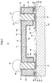
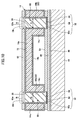
- Fig. 1 is a vertical cross-sectional view illustrating an electronic device 10 to which an embedment of a through electrode and a method for forming the same according to the present invention are applied.
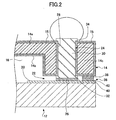
- Fig. 2 is an enlarged vertical cross-sectional view illustrating the through electrode.
- a function element 18 serving as a micromachine part is formed in an element mount space 16 defined by a substrate 12 and a lid (substrate) 14.
- the substrate 12 may be, for example, a silicon wafer (silicon substrate) or a glass substrate. If silicon is used as the substrate 12, a silicon wafer or glass is preferable as a support body described below. This embodiment is applicable for forming through electrodes not only in simple substrates but also in semiconductor wafers with integrated circuits.
- an electronic circuit for operating the function element 18 is formed on the surface of the substrate 12, in addition to the function element 18 including a cantilever.
- the electronic circuit includes electrodes 20 made of aluminum (Al) or copper (Cu).
- the function element 18 is formed on the surface of the substrate 12 by a micromachining method.
- the electronic device 10 may be used as, for example, a sensor such as accelerometer and a micro gyro in accordance with the configuration of the function element 18 mounted on the substrate 12.
- the electronic device 10 includes ultrasonic joint sections 22 for electrically joining the substrate 12 to the lid 14.
- the lid 14 includes a substrate 14a made of a Si wafer having a surface coated with an insulating layer 15, a recess 14b defining the element mount space 16, and a frame 14c surrounding the recess 14b.
- Each of the ultrasonic joint sections 22 comprises the electrode 20, a through electrode 24 formed in the lid 14, and a bump 26 made of gold for connecting a lower end of the through electrode 24 to the electrode 20.
- a solder bump 27 is formed on an upper end of the through electrode 24.
- the frame 14c of the lid 14 is provided with through holes 28 in which the through electrodes 24 are formed.
- the through holes 28 have hole diameters of 30 ⁇ m through 100 ⁇ m and heights (corresponding to the thickness of the substrate 14a) of 150 ⁇ m through 500 ⁇ m. Accordingly, the aspect ratio (thickness/hole diameter) of this embodiment ranges from 1.5 through 16.67.
- the through electrode 24 integrally comprises a columnar electrode 30 filling the through hole 28, a lower end electrode pad 32 formed on a lower end side of the columnar electrode 30 and having a size (horizontal surface area) wider than the cross section of the through hole 28, and an upper end electrode pad 34 formed on an upper end side of the columnar electrode 30 and having a size wider than the cross section of the through hole 28.
- the electronic device 10 is provided with an ultrasonic joint section 36 for sealing between a periphery of four edges of the lid 14 and a periphery of four edges of the substrate 12.
- the ultrasonic joint section 36 seals the element mount space 16 by joining, through a gold bump 42, quadrangular sealing pattern 38 formed on a lower face periphery of the lid 14 and a quadrangular sealing pattern 40 formed on an upper face periphery of the substrate 12.
- the sealing pattern 38 is made of copper, while the sealing pattern 40 is made of copper or aluminum (Al).
- the sealing patterns 38 and 40 are integrally joined by Au-Cu bonding through the gold bump 42 or gold plating.
- the lower end electrode pad 32 and the upper end electrode pad 34 each have a size wider than the cross section of the through hole 28, so that the through hole 28 is tightly sealed. This contributes to ensuring airtightness of the element mount space 16.
- the lower end electrode pad 32 and the upper end electrode pad 34 each have a surface area wider than the hole diameter of the through hole 28. The wider surface area, which is used as a connection area, facilitates connecting work with, for example, soldering.
- a film-type adhesive tape 46 is applied to the surface of a Si wafer 44, which serves as a support body, by a lamination method.
- the adhesive tape 46 which is a two-sided adhesive tape having an adhesive layer on each of an upper face and a lower face thereof, tightly adheres to the surface of the Si wafer 44.
- the adhesive tape 46 serves to join a photoresist layer (adhesive layer) 52 described below and the Si wafer 44.
- the adhesive tape 46 becomes removable when the contact area is reduced due to explosion of micro capsules in a heat treatment performed after the through electrode 24 is completed.
- a seed layer 48 is formed on an upper face of the adhesive tape 46 applied to the surface of the Si wafer 44.
- An example of a method for forming the seed layer 48 includes a method for forming a coating of copper (Cu) by vacuum deposition or sputtering, and a method for laminating a metal foil such as a Cu foil.
- a dry film 50 is applied to the surface of the seed layer 48 by a lamination method or by roller pressing.
- the dry film 50 has a double layer structure in which a passivation film (PET: polyethylene terephthalate) 53 is joined to an upper face of the photoresist layer 52 used as an adhesive layer.
- PET polyethylene terephthalate
- the photoresist layer 52 tightly adheres to the surface of the seed layer 48.
- the photoresist layer 52 is a negative resist film made of a photosensitive organic material that loses adhesiveness upon exposure and allows an unexposed part thereof to be dissolved and removed by developer.
- the photoresist layer 52 is formed by applying the dry film 50 to the surface of the seed layer 48 in this embodiment, the photoresist layer 52 may be formed by other methods, such as printing, without using the dry film 50. Instead of using the photoresist layer 52, an adhesive agent made of epoxy resin or polyimide resin may be used as the adhesive layer.
- the passivation film 53 of the dry film 50 is peeled and separated from the photoresist layer 52.
- the upper face and the lower face of the photoresist layer 52 have adhesiveness, and the adhesion between the lower face of the photoresist layer 52 and the seed layer 48 is stronger than the adhesion between the upper face of the photoresist layer 52 and the passivation film 53. Therefore, when the passivation film 53 is peeled off, the photoresist layer 52 is not separated from the seed layer 48.
- the photoresist layer 52 has a thickness ranging about from 10 ⁇ m through 15 ⁇ m, which corresponds to the thickness of the lower end electrode pad 32 as described below.
- step 5A shown in Fig. 7 the lid 14 made of a Si wafer is mounted on the adhesive surface of the photoresist layer 52.
- the recess 14b forming the element mount space 16 in the center of the lower face of the lid 14 is formed in the lid 14.
- the plural through holes 28 are formed to vertically extend through the frame 14c protruding downward and surrounding the recess 14b.
- the lid 14 is pressed onto the photoresist layer 52, so that the lower face of the frame 14c is press-bonded to the adhesive surface of the photoresist layer 52.
- the lid 14 is directly press-bonded to the surface of the photoresist layer 52 without using an adhesive tape, thereby eliminating a need for applying an adhesive tape and simplifying the production process.
- step 6A shown in Fig. 8 developer is provided into each of the through holes 28 so as to dissolve the photoresist layer 52 in an area A opposing a lower opening of the through hole 28.
- a dip development system for dipping the lid 14 mounted on the Si wafer 44 into the developer or a spray development system for spraying the developer onto the lid 14 from the upper side thereof may be applicable. Both of these development systems can dissolve the photoresist layer 52 in the area A opposing the lower opening of the through hole 28 and, therefore, can form a flange clearance 54 with a width Da (>D) greater than the inside diameter D of the through hole 28 while controlling infiltration time.
- step 7A shown in Fig. 9 the surface of the seed layer 48 exposed at the bottom of the through hole 28 is gold plated to form an Au plating layer 56 serving as barrier metal that prevents diffusion of the through electrode 24. Then, an upper face of the Au plating layer 56 is nickel plated, so that a Ni plating layer 58 is formed. Subsequently, copper is deposited on the Ni plating layer 58 by an electrolytic plating method, so that a columnar section 60b of a stud via 60 is formed inside the through hole 28. The stud via 60 is formed from bottom to top in the through hole 28 by depositing copper on the surface of the Ni plating layer 58 serving as a base. This prevents formation of voids near the center of the stud via 60 and can fill up the through hole 28 to its upper opening by depositing copper into the through hole 28.
- the size of the Au plating layer 56 and the Ni plating layer 58 is wider than the cross section of the through hole 28.
- a Cu flange section 60a of the stud via 60 deposited on the Ni plating layer 58 also has a size wider than the cross section of the through hole 28.
- the Au plating layer 56, the Ni plating layer 58, and the Cu flange section 60a constitute the lower end electrode pad 32.
- the Cu columnar section 60b deposited on the Cu flange section 60a corresponds to the columnar electrode 30.
- the plating structure of the electrode pad 32 may be a double layer plating structure of nickel and palladium (palladium on the top side) or may be a three-layer plating structure of nickel, palladium, and gold (gold on the top side).
- a dry film is applied to an upper face of the lid 14 by a lamination method to form a negative resist layer 62.
- the negative resist layer 62 in an area B opposing an upper end of the stud via 60 is exposed and cured, and an unexposed part of the negative resist layer 62 is removed by developer. With this patterning process, a part of the negative resist layer 62 of an area wider than the upper opening of the through hole 28 is dissolved.
- a flange clearance 62a continuous to the upper end of the stud via 60 (upper side of the through hole 28) is formed.
- the flange clearance 62a formed in the negative resist layer 62 has a width Db (>D) greater than the inside diameter D of the through hole 28.
- a Cu flange section 60c is formed on the upper end of the Cu columnar section 60b by electrolytic plating.
- the Cu flange section 60c has an area wider than the cross section of the through hole 28, because the Cu flange section 60c is formed in the flange clearance 62a having an area wider than the cross section of the through hole 28.
- a Ni plating layer 64 is formed on an upper face of the Cu flange section 60c by electrolytic plating.
- an electrolytic Au plating layer (or Sn plating layer) 66 serving as barrier metal is formed on an upper face of the Ni plating layer 64 by electrolytic gold plating.
- the Au plating layer (or Sn plating layer) 66, the Ni plating layer 64, and the Cu flange section 60c constitute the upper end electrode pad 34.
- the plating structure of the electrode pad 34 may be a double layer plating structure of nickel and palladium (palladium on the top side) or may be a three-layer plating structure of nickel, palladium, and gold (gold on the top side).
- step 10A shown in Fig. 12 the exposed part of the negative resist layer 62 on the lid 14 is removed by swelling with use of remover (e.g. alkaline solution, caustic soda, etc.).
- remover e.g. alkaline solution, caustic soda, etc.
- step 11A shown in Fig. 13 the Si wafer 44 is heated to a high temperature in a baking process, so that the microcapsules contained in the adhesive tape 46 are exploded.
- the contact area of the adhesive tape 46 is reduced. Therefore, the Si wafer 44 bonded to the seed layer 48 through the adhesive tape 46 becomes easily separable from the seed layer 48.
- the Si wafer 44 may be removed by buffing.
- step 12A shown in Fig. 14 the seed layer 48 is removed by etching. Then, the photoresist layer 52 bonded to the lower face of the lid is removed by using remover (e.g. alkaline solution, caustic soda, etc.) In this way, the lid 14 having the through electrodes 24 is completed.
- remover e.g. alkaline solution, caustic soda, etc.
- the through electrode 24 formed by the above-described forming method has a configuration in which the columnar electrode 30 filling the through hole 28 extending through the substrate 14a of the lid 14, the lower end electrode pad 32 formed on the lower end side of the columnar electrode 30 and having an area wider than the cross section of the through hole 28, and the upper end electrode pad 34 formed on the upper end side of the columnar electrode 30 and having an area wider than the cross section of the through hole 28 are integrally joined. Therefore, both upper and lower ends of the through hole 28 are tightly sealed. Moreover, as the columnar electrode 30 is formed from bottom to top on the lower end electrode pad 32, formation of voids near the center of the through hole 28 is prevented. Therefore, the columnar electrode 30 can be stably formed in the through hole 28 even if the aspect ratio (thickness/hole diameter) is high.
- the seed layer 48 is formed on the surface of the Si wafer 44 with the adhesive tape 46 interposed therebetween. Therefore, after the through electrode 24 is formed, the Si wafer 44 can be easily separated from the seed layer 48 by heating the adhesive tape 46. This simplifies a production process, and lowers production costs.
- step 1B shown in Fig. 15 a glass wafer 70 serving as a support body is prepared.
- a seed layer 48 is formed on an upper face of the glass wafer 70.
- An example of a method for forming the seed layer 48 includes vacuum deposition or sputtering of copper or nickel.
- step 3B shown in Fig. 17 a dry film 50 is applied to the surface of the seed layer 48 by a lamination method.
- step 4B shown in Fig. 18 a passivation film 53 of the dry film 50 is peeled and separated from a photoresist layer 52.
- step 5B shown in Fig. 19 the lid 14 made of a Si wafer is attached on an adhesive surface of the photoresist layer 52.
- a recess 14b forming an element mount space 16 (see Fig. 1) in the center on a lower face of the lid 14 is formed in the lid 14.
- Through holes 28 are formed to vertically extend through a frame 14c protruding downward and surrounding the recess 14b.
- the lid 14 is pressed onto the photoresist layer 52, so that a lower face of the frame 14c is press-bonded to the adhesive surface of the photoresist layer 52.
- step 6B shown in Fig. 20 developer is provided into each of the through holes 28 so as to dissolve the photoresist layer 52 in an area A (see Fig. 8) opposing a lower opening of the through hole 28.
- the developer provided into the through hole 28 can dissolve the photoresist layer 52 in the area A opposing the lower opening of the through hole 28 and, therefore, can form a flange clearance 54 with a width Da (>D) (see Fig. 8) greater than the inside diameter D of the through hole 28 while controlling infiltration time.
- plasma ashing is performed to generate active oxygen atoms in the dissolved photoresist layer 52 in the area A by electron collision dissociation utilizing plasma.
- the photoresist layer 52 is removed from the flange clearance 54.
- the plasma ashing improves the wetting efficiency of a plating solution in plating processing in the next step.
- step 7B shown in Fig. 21 the surface of the seed layer 48 exposed at the bottom of the through hole 28 is gold plated to form an Au plating layer 56 serving as barrier metal that prevents diffusion of the through electrode 24. Then, an upper face of the Au plating layer 56 is nickel plated, so that a Ni plating layer 58 is formed. Subsequently, copper is deposited on the Ni plating layer 58 by an electrolytic plating method, so that a columnar section 60b of a stud via 60 is formed inside the through hole 28. The stud via 60 is formed bottom to top in the through hole 28 by depositing copper on the surface of the Ni plating layer 58 serving as a base. This prevents formation of voids near the center of the stud via 60 and can fill up the through hole 28 to the upper opening of by depositing copper into the through hole 28.
- the area of the Au plating layer 56 and the Ni plating layer 58 is wider than the cross section of the through hole 28.
- a Cu flange section 60a of the stud via 60 deposited on the Ni plating layer 58 also has an area wider than the cross section of the through hole 28.
- a dry film is applied to an upper face of the lid 14 by a lamination method to form a negative resist layer 62.
- the negative resist layer 62 in an area B opposing an upper end of the stud via 60 is exposed and cured, and an unexposed part of the negative resist layer 62 is removed by developer. With this patterning process, a part of the negative resist layer 62 of an area wider than the upper opening of the through hole 28 is dissolved. Thus, a flange clearance 62a continuous to the upper end of the stud via 60 (upper side of the through hole 28) is formed.
- the flange clearance 62a formed in the negative resist layer 62 has a width Db (>D) greater than the inside diameter D of the through hole 28.
- a Cu flange section 60c is formed on the upper end of the Cu columnar section 60b by plating.
- the Cu flange section 60c has an area wider than the cross section of the through hole 28, because the Cu flange section 60c is formed in the flange clearance 62a having an area wider than the cross section of the through hole 28.
- a Ni plating layer 64 is formed on the upper face of the Cu flange section 60c by electroless plating.
- an electrolytic Au plating layer (or Sn plating layer) 66 serving as barrier metal is formed on an upper face of the Ni plating layer 64 by electroless plating.
- step 10B shown in Fig. 24 the exposed negative resist layer 62 on the lid 14 is removed therefrom by swelling with use of a remover (e.g. alkaline solution, caustic soda, etc.).
- a remover e.g. alkaline solution, caustic soda, etc.
- the glass wafer 70 is heated to a high temperature from the lower side in a baking process, so that the photoresist layer 52 is cured. The photoresist layer 52 thus loses adhesiveness, so that the photoresist layer 52 becomes easily separable from the lid 14.
- step 12B shown in Fig. 26 the glass wafer 70 is separated to the lower side, so that the photoresist layer 52 is separated from the lower surface of the lid 14. In this way, the lid 14 having the through electrodes 24 is completed.
- the photoresist layer 52 may be separated from the lower face of the lid 14 by removing the glass wafer 70 by grinding, and then removing the seed layer 48 by etching.
- the through electrode 24 formed by the above-described forming method has a configuration in which the columnar electrode 30 filling the through hole 28 extending through the substrate 14a of the lid 14, the lower end electrode pad 32 formed on the lower end side of the columnar electrode 30 and having an area wider than the cross section of the through hole 28, and the upper end electrode pad 34 formed on the upper end side of the columnar electrode 30 and having an area wider than the cross section of the through hole 28 are integrally joined. Therefore, both upper and lower ends of the through hole 28 are tightly sealed. Moreover, as the columnar electrode 30 is formed from bottom to top on the lower end electrode pad 32, formation of voids near the center of the through hole 28 is prevented. Therefore, the columnar electrode 30 can be stably formed in the through hole 28 even if the aspect ratio (thickness/hole diameter) is high.
- the glass wafer 70 can be easily separated from the lid 14 by heating the photoresist layer 52 formed on the surface of the glass wafer 70 with the seed layer 48 interposed therebetween. This simplifies a production process, and lowers production costs.
- micromachine packages for electronic devices are exemplified in the above embodiments, the present invention is also applicable to electrodes used in other products (e.g. interposers and products having through holes for connecting upper face side wiring patterns and lower face side wiring patterns).
Abstract
Description
- The present invention relates to a through electrode and a method for forming the same, and particularly relates to a through electrode adapted to fill a small hole with a conductive material and a method for forming the same.
- Electronic devices having three-dimensional structures, such as micromachine packages and interposers, called as MEMS (Micro Electro Mechanical Systems), and utilizing semiconductor microprocessing technologies are known. In recent years, techniques for forming through electrodes that connect an upper wiring pattern to a lower wiring pattern in such an electronic device have been developed. For example, in some interposers, through electrodes are formed in through holes extending between an upper face and a lower face of a substrate so as to provide electrical connection between wiring patterns (see, for example, Japanese Patent Laid-Open Publication No. 1-258457).
- This publication discloses a method for filling through holes, which are formed in a substrate covered with insulating film, with metal by plating. According to this method, a seed layer is formed on an upper face of a substrate by a sputtering method. Then, an electrode for plating is brought into contact with an upper face of the seed layer to deposit conductive metal, such as Cu, onto the surface of the seed layer using an electrolytic plating method. A conductor layer formed of the conductive metal is then grown, so that the through holes are filled with metal.
- However, the method described above has a problem that, because the conductor layer formed on the surface of the seed layer is formed on the inner surfaces of the through holes and grows on the inner surfaces of the through holes, voids are formed near the center of the individual through holes along with the growth of the conductor layer.
- Especially, in the case of micromachine packages, when the diameter of a through hole relative to the thickness of a substrate is small and accordingly the aspect ratio (thickness/hole diameter) is high, it is difficult to form a through electrode in such a small through hole.
- A general object of the present invention is to provide a through electrode and a method for forming the same to solve at least one problem described above.
- According to an aspect of the present invention, there is provided a method for forming a through electrode, comprising a first step of forming a seed layer on a surface of a support body, a second step of forming an adhesive layer on a surface of the seed layer, a third step of pressing a substrate having a through hole formed therein onto the adhesive layer, a fourth step of removing a portion of the adhesive layer that communicates with the through hole of the substrate by a development process to form a clearance wider than a cross section of the through hole at a lower end of the through hole; a fifth step of filling the clearance and the through hole with a conductor to form a lower end electrode pad covering the lower end of the through hole and a columnar electrode filling the through hole; and a sixth step of removing the support body, the seed layer, and the adhesive layer from the substrate.
- The fifth step preferably includes a step of forming an Au layer constituting the lower end electrode pad on the surface of the seed layer, a step of forming a Ni layer on a surface of the Au layer, and a step of laminating a Cu layer on a surface of the Ni layer to form the columnar electrode.
- It is preferable that an adhesive tape be applied to the surface of the support body, and then the seed layer be formed on an adhesive face of the adhesive layer in the first step; and after the columnar electrode is formed in the fifth step, the support body be separated from the seed layer by heating the adhesive tape in the sixth step.
- It is also preferable that the seed layer be formed on the surface of the support body in the first step, and then the adhesive layer be formed on the seed layer; and after the columnar electrode is formed inside the through hole in the fifth step, the support body be separated from the seed layer by heating the adhesive layer in the sixth step.
- It is also preferable that the adhesive layer include a photoresist layer; and the fourth step include a step of removing the photoresist layer formed in the area communicating with the through hole of the substrate by a development process, and a step of forming the clearance wider than the cross section of the through hole at the lower end of the through hole.
- It is preferable that the method for forming a through electrode further comprise a step of laminating a resist layer on an upper face of the substrate and forming an opening wider than the cross section of the through hole at an upper end of the through hole in the resist layer, a step of filling the opening of the resist layer with a conductor to form an upper end electrode pad continuous to an upper end of the columnar electrode, and a step of removing the resist layer surrounding the upper end electrode pad.
- According to another aspect of the present invention, there is provided an electrode that is inserted in a through hole extending through a substrate and electrically connects a conductor pattern formed on an upper face of the substrate to a conductor pattern formed on a lower face of the substrate, comprising a lower end electrode pad wider than a cross section of the through hole and configured to seal a lower end opening of the through hole, and a columnar electrode formed from bottom to top so as to fill the through hole by laminating a conductive material on the lower end electrode pad.
- It is preferable that an upper end electrode pad wider than the cross section of the through hole and configured to seal an upper end opening of the through hole be formed on an upper end of the columnar electrode.
- According to the present invention, the seed layer is formed on the surface of the support body, and the substrate is mounted on the adhesive layer formed on the surface of the seed layer. There is no need to separately provide an adhesive layer for fixing the substrate, thereby simplifying a production process and lowering production costs. The adhesive layer formed in the area communicating with the through hole of the substrate is removed by development to form a clearance wider than the cross section of the through hole at the lower end of the through hole. Therefore, the lower end electrode pad covering the lower end of the through hole can be formed in the clearance opposing the seed layer. Moreover, because the columnar electrode is formed from bottom to top on the lower end electrode pad, formation of voids near the center of the through hole is prevented. As such, the columnar electrode can be stably formed even if the aspect ratio (thickness/hole diameter) is high.
- As the seed layer is formed on the surface of the support body with the adhesive tape interposed therebetween, the support body is easily separable from the seed layer by heating the adhesive tape after forming the through electrode.
- Also, as the adhesive layer is formed on the surface of the support body with the seed layer interposed therebetween, the support body is easily separable from the substrate by heating the adhesive layer.
-
- Fig. 1 is a vertical cross-sectional view illustrating an electronic device to which an embedment of a through electrode and a method for forming the same according to the present invention are applied;
- Fig. 2 is an enlarged vertical cross-sectional view illustrating a through electrode;
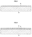
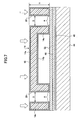
- Figs. 3 - 14 are vertical cross-sectional views illustrating processes of a first embodiment; and
- Figs. 15 - 26 are vertical cross-sectional views illustrating processes of a second embodiment.
- The following description provides exemplary embodiments of the present invention with reference to the accompanying drawings.
- Fig. 1 is a vertical cross-sectional view illustrating an
electronic device 10 to which an embedment of a through electrode and a method for forming the same according to the present invention are applied. Fig. 2 is an enlarged vertical cross-sectional view illustrating the through electrode. - In the
electronic device 10, as shown in Fig. 1, afunction element 18 serving as a micromachine part is formed in anelement mount space 16 defined by asubstrate 12 and a lid (substrate) 14. Each of thesubstrate 12, thelid 14, and theelement mount space 16 has a quadrangular shape when viewed from the top. According to this embodiment, thesubstrate 12 may be, for example, a silicon wafer (silicon substrate) or a glass substrate. If silicon is used as thesubstrate 12, a silicon wafer or glass is preferable as a support body described below. This embodiment is applicable for forming through electrodes not only in simple substrates but also in semiconductor wafers with integrated circuits. - Although not shown in Fig. 1, an electronic circuit for operating the
function element 18 is formed on the surface of thesubstrate 12, in addition to thefunction element 18 including a cantilever. The electronic circuit includeselectrodes 20 made of aluminum (Al) or copper (Cu). Thefunction element 18 is formed on the surface of thesubstrate 12 by a micromachining method. - The
electronic device 10 according to this embodiment may be used as, for example, a sensor such as accelerometer and a micro gyro in accordance with the configuration of thefunction element 18 mounted on thesubstrate 12. - The
electronic device 10 includesultrasonic joint sections 22 for electrically joining thesubstrate 12 to thelid 14. Thelid 14 includes asubstrate 14a made of a Si wafer having a surface coated with aninsulating layer 15, arecess 14b defining theelement mount space 16, and aframe 14c surrounding therecess 14b. Each of theultrasonic joint sections 22 comprises theelectrode 20, a throughelectrode 24 formed in thelid 14, and abump 26 made of gold for connecting a lower end of the throughelectrode 24 to theelectrode 20. Asolder bump 27 is formed on an upper end of the throughelectrode 24. - The
frame 14c of thelid 14 is provided with throughholes 28 in which thethrough electrodes 24 are formed. The throughholes 28 have hole diameters of 30 µm through 100 µm and heights (corresponding to the thickness of thesubstrate 14a) of 150 µm through 500 µm. Accordingly, the aspect ratio (thickness/hole diameter) of this embodiment ranges from 1.5 through 16.67. - As shown in Fig. 2, the through
electrode 24 integrally comprises acolumnar electrode 30 filling the throughhole 28, a lowerend electrode pad 32 formed on a lower end side of thecolumnar electrode 30 and having a size (horizontal surface area) wider than the cross section of the throughhole 28, and an upperend electrode pad 34 formed on an upper end side of thecolumnar electrode 30 and having a size wider than the cross section of the throughhole 28. - The
electronic device 10 is provided with anultrasonic joint section 36 for sealing between a periphery of four edges of thelid 14 and a periphery of four edges of thesubstrate 12. Theultrasonic joint section 36 seals theelement mount space 16 by joining, through agold bump 42,quadrangular sealing pattern 38 formed on a lower face periphery of thelid 14 and aquadrangular sealing pattern 40 formed on an upper face periphery of thesubstrate 12. Thesealing pattern 38 is made of copper, while thesealing pattern 40 is made of copper or aluminum (Al). Thesealing patterns gold bump 42 or gold plating. - Because the through
electrode 24 comprises the lowerend electrode pad 32 arranged to seal a lower end opening of the throughhole 28 and thecolumnar electrode 30 filling the throughhole 28 by lamination of copper (conductive material) on the lowerend electrode pad 32, formation of voids in the center of thecolumnar electrode 30 is prevented. Therefore, thecolumnar electrode 30 can be stably formed even if the aspect ratio (thickness/hole diameter) is high. - The lower
end electrode pad 32 and the upperend electrode pad 34 each have a size wider than the cross section of the throughhole 28, so that the throughhole 28 is tightly sealed. This contributes to ensuring airtightness of theelement mount space 16. The lowerend electrode pad 32 and the upperend electrode pad 34 each have a surface area wider than the hole diameter of the throughhole 28. The wider surface area, which is used as a connection area, facilitates connecting work with, for example, soldering. - The following describes a method for forming the through
electrode 24 with reference to Figs. 3 - 14. - In step 1A shown in Fig. 3, a film-type
adhesive tape 46 is applied to the surface of aSi wafer 44, which serves as a support body, by a lamination method. Theadhesive tape 46, which is a two-sided adhesive tape having an adhesive layer on each of an upper face and a lower face thereof, tightly adheres to the surface of theSi wafer 44. Theadhesive tape 46 serves to join a photoresist layer (adhesive layer) 52 described below and theSi wafer 44. Theadhesive tape 46 becomes removable when the contact area is reduced due to explosion of micro capsules in a heat treatment performed after the throughelectrode 24 is completed. - In step 2A shown in Fig. 4, a
seed layer 48 is formed on an upper face of theadhesive tape 46 applied to the surface of theSi wafer 44. An example of a method for forming theseed layer 48 includes a method for forming a coating of copper (Cu) by vacuum deposition or sputtering, and a method for laminating a metal foil such as a Cu foil. - In step 3A shown in Fig. 5, a
dry film 50 is applied to the surface of theseed layer 48 by a lamination method or by roller pressing. Thedry film 50 has a double layer structure in which a passivation film (PET: polyethylene terephthalate) 53 is joined to an upper face of thephotoresist layer 52 used as an adhesive layer. Thephotoresist layer 52 tightly adheres to the surface of theseed layer 48. Thephotoresist layer 52 is a negative resist film made of a photosensitive organic material that loses adhesiveness upon exposure and allows an unexposed part thereof to be dissolved and removed by developer. Although thephotoresist layer 52 is formed by applying thedry film 50 to the surface of theseed layer 48 in this embodiment, thephotoresist layer 52 may be formed by other methods, such as printing, without using thedry film 50. Instead of using thephotoresist layer 52, an adhesive agent made of epoxy resin or polyimide resin may be used as the adhesive layer. - In step 4A shown in Fig. 6, the
passivation film 53 of thedry film 50 is peeled and separated from thephotoresist layer 52. The upper face and the lower face of thephotoresist layer 52 have adhesiveness, and the adhesion between the lower face of thephotoresist layer 52 and theseed layer 48 is stronger than the adhesion between the upper face of thephotoresist layer 52 and thepassivation film 53. Therefore, when thepassivation film 53 is peeled off, thephotoresist layer 52 is not separated from theseed layer 48. Thephotoresist layer 52 has a thickness ranging about from 10 µm through 15 µm, which corresponds to the thickness of the lowerend electrode pad 32 as described below. - In step 5A shown in Fig. 7, the
lid 14 made of a Si wafer is mounted on the adhesive surface of thephotoresist layer 52. As previously mentioned, therecess 14b forming theelement mount space 16 in the center of the lower face of thelid 14 is formed in thelid 14. The plural throughholes 28 are formed to vertically extend through theframe 14c protruding downward and surrounding therecess 14b. Thelid 14 is pressed onto thephotoresist layer 52, so that the lower face of theframe 14c is press-bonded to the adhesive surface of thephotoresist layer 52. In step 5A, thelid 14 is directly press-bonded to the surface of thephotoresist layer 52 without using an adhesive tape, thereby eliminating a need for applying an adhesive tape and simplifying the production process. - In this embodiment, because the
photoresist layer 52 remains unexposed, thephotoresist layer 52 is kept fixed to thelid 14 without losing the adhesiveness in the following processes. The throughhole 28 of this embodiment has an inside diameter of about D=30 µm through 60 µm and a height (corresponding to the thickness of theframe 14c) of about H=100 µm through 200 µm. - In step 6A shown in Fig. 8, developer is provided into each of the through
holes 28 so as to dissolve thephotoresist layer 52 in an area A opposing a lower opening of the throughhole 28. For providing the developer into the throughhole 28 for development, a dip development system for dipping thelid 14 mounted on theSi wafer 44 into the developer or a spray development system for spraying the developer onto thelid 14 from the upper side thereof may be applicable. Both of these development systems can dissolve thephotoresist layer 52 in the area A opposing the lower opening of the throughhole 28 and, therefore, can form aflange clearance 54 with a width Da (>D) greater than the inside diameter D of the throughhole 28 while controlling infiltration time. - In other words, the developer infiltrates from the surface of the
photoresist layer 52 in the area A opposing the lower opening of the throughhole 28 in the thickness direction to dissolve thephotoresist layer 52. As the infiltration time is extended, the developer infiltrates also in the radial direction of the area A to dissolve an area of thephotoresist layer 52 larger than the lower opening of the throughhole 28. The infiltration time is set in accordance with an infiltration speed which varies depending on a combination of the material of thephotoresist layer 52 and the type of the developer. - Then, plasma ashing is performed to generate active oxygen atoms in the dissolved
photoresist layer 52 in the area A by electron collision dissociation utilizing plasma. Thus, thephotoresist layer 52 is removed from theflange clearance 54. The plasma ashing improves the wetting efficiency of a plating solution in plating processing in the next step. - In step 7A shown in Fig. 9, the surface of the
seed layer 48 exposed at the bottom of the throughhole 28 is gold plated to form anAu plating layer 56 serving as barrier metal that prevents diffusion of the throughelectrode 24. Then, an upper face of theAu plating layer 56 is nickel plated, so that aNi plating layer 58 is formed. Subsequently, copper is deposited on theNi plating layer 58 by an electrolytic plating method, so that acolumnar section 60b of a stud via 60 is formed inside the throughhole 28. The stud via 60 is formed from bottom to top in the throughhole 28 by depositing copper on the surface of theNi plating layer 58 serving as a base. This prevents formation of voids near the center of the stud via 60 and can fill up the throughhole 28 to its upper opening by depositing copper into the throughhole 28. - Because the
Au plating layer 56 and theNi plating layer 58 are formed in theflange clearance 54, the size of theAu plating layer 56 and theNi plating layer 58 is wider than the cross section of the throughhole 28. ACu flange section 60a of the stud via 60 deposited on theNi plating layer 58 also has a size wider than the cross section of the throughhole 28. TheAu plating layer 56, theNi plating layer 58, and theCu flange section 60a constitute the lowerend electrode pad 32. TheCu columnar section 60b deposited on theCu flange section 60a corresponds to thecolumnar electrode 30. The plating structure of theelectrode pad 32 may be a double layer plating structure of nickel and palladium (palladium on the top side) or may be a three-layer plating structure of nickel, palladium, and gold (gold on the top side). In step 8A shown in Fig. 10, a dry film is applied to an upper face of thelid 14 by a lamination method to form a negative resistlayer 62. The negative resistlayer 62 in an area B opposing an upper end of the stud via 60 is exposed and cured, and an unexposed part of the negative resistlayer 62 is removed by developer. With this patterning process, a part of the negative resistlayer 62 of an area wider than the upper opening of the throughhole 28 is dissolved. Thus, aflange clearance 62a continuous to the upper end of the stud via 60 (upper side of the through hole 28) is formed. Theflange clearance 62a formed in the negative resistlayer 62 has a width Db (>D) greater than the inside diameter D of the throughhole 28. - In step 9A shown in Fig. 11, a
Cu flange section 60c is formed on the upper end of theCu columnar section 60b by electrolytic plating. TheCu flange section 60c has an area wider than the cross section of the throughhole 28, because theCu flange section 60c is formed in theflange clearance 62a having an area wider than the cross section of the throughhole 28. ANi plating layer 64 is formed on an upper face of theCu flange section 60c by electrolytic plating. Then, an electrolytic Au plating layer (or Sn plating layer) 66 serving as barrier metal is formed on an upper face of theNi plating layer 64 by electrolytic gold plating. The Au plating layer (or Sn plating layer) 66, theNi plating layer 64, and theCu flange section 60c constitute the upperend electrode pad 34. - The plating structure of the
electrode pad 34 may be a double layer plating structure of nickel and palladium (palladium on the top side) or may be a three-layer plating structure of nickel, palladium, and gold (gold on the top side). - In step 10A shown in Fig. 12, the exposed part of the negative resist
layer 62 on thelid 14 is removed by swelling with use of remover (e.g. alkaline solution, caustic soda, etc.). - In step 11A shown in Fig. 13, the
Si wafer 44 is heated to a high temperature in a baking process, so that the microcapsules contained in theadhesive tape 46 are exploded. When the micro capsules contained in theadhesive tape 46 are exploded, the contact area of theadhesive tape 46 is reduced. Therefore, theSi wafer 44 bonded to theseed layer 48 through theadhesive tape 46 becomes easily separable from theseed layer 48. - Other methods may be used for separating the
Si wafer 44 without being limited to the above method. For example, theSi wafer 44 may be removed by buffing. - In step 12A shown in Fig. 14, the
seed layer 48 is removed by etching. Then, thephotoresist layer 52 bonded to the lower face of the lid is removed by using remover (e.g. alkaline solution, caustic soda, etc.) In this way, thelid 14 having the throughelectrodes 24 is completed. - The through
electrode 24 formed by the above-described forming method has a configuration in which thecolumnar electrode 30 filling the throughhole 28 extending through thesubstrate 14a of thelid 14, the lowerend electrode pad 32 formed on the lower end side of thecolumnar electrode 30 and having an area wider than the cross section of the throughhole 28, and the upperend electrode pad 34 formed on the upper end side of thecolumnar electrode 30 and having an area wider than the cross section of the throughhole 28 are integrally joined. Therefore, both upper and lower ends of the throughhole 28 are tightly sealed. Moreover, as thecolumnar electrode 30 is formed from bottom to top on the lowerend electrode pad 32, formation of voids near the center of the throughhole 28 is prevented. Therefore, thecolumnar electrode 30 can be stably formed in the throughhole 28 even if the aspect ratio (thickness/hole diameter) is high. - In this embodiment, the
seed layer 48 is formed on the surface of theSi wafer 44 with theadhesive tape 46 interposed therebetween. Therefore, after the throughelectrode 24 is formed, theSi wafer 44 can be easily separated from theseed layer 48 by heating theadhesive tape 46. This simplifies a production process, and lowers production costs. - The following describes a second embodiment of a method for forming the through
electrode 24 with reference to Figs. 15 - 26. In the second embodiment, elements identical to those in the first embodiment bear the same reference numerals. - In step 1B shown in Fig. 15, a
glass wafer 70 serving as a support body is prepared. - In step 2B shown in Fig. 16, a
seed layer 48 is formed on an upper face of theglass wafer 70. An example of a method for forming theseed layer 48 includes vacuum deposition or sputtering of copper or nickel. - In step 3B shown in Fig. 17, a
dry film 50 is applied to the surface of theseed layer 48 by a lamination method. - In step 4B shown in Fig. 18, a
passivation film 53 of thedry film 50 is peeled and separated from aphotoresist layer 52. - In step 5B shown in Fig. 19, the
lid 14 made of a Si wafer is attached on an adhesive surface of thephotoresist layer 52. Arecess 14b forming an element mount space 16 (see Fig. 1) in the center on a lower face of thelid 14 is formed in thelid 14. Throughholes 28 are formed to vertically extend through aframe 14c protruding downward and surrounding therecess 14b. Thelid 14 is pressed onto thephotoresist layer 52, so that a lower face of theframe 14c is press-bonded to the adhesive surface of thephotoresist layer 52. - In step 6B shown in Fig. 20, developer is provided into each of the through
holes 28 so as to dissolve thephotoresist layer 52 in an area A (see Fig. 8) opposing a lower opening of the throughhole 28. The developer provided into the throughhole 28 can dissolve thephotoresist layer 52 in the area A opposing the lower opening of the throughhole 28 and, therefore, can form aflange clearance 54 with a width Da (>D) (see Fig. 8) greater than the inside diameter D of the throughhole 28 while controlling infiltration time. - Then, plasma ashing is performed to generate active oxygen atoms in the dissolved
photoresist layer 52 in the area A by electron collision dissociation utilizing plasma. Thus, thephotoresist layer 52 is removed from theflange clearance 54. The plasma ashing improves the wetting efficiency of a plating solution in plating processing in the next step. - In step 7B shown in Fig. 21, the surface of the
seed layer 48 exposed at the bottom of the throughhole 28 is gold plated to form anAu plating layer 56 serving as barrier metal that prevents diffusion of the throughelectrode 24. Then, an upper face of theAu plating layer 56 is nickel plated, so that aNi plating layer 58 is formed. Subsequently, copper is deposited on theNi plating layer 58 by an electrolytic plating method, so that acolumnar section 60b of a stud via 60 is formed inside the throughhole 28. The stud via 60 is formed bottom to top in the throughhole 28 by depositing copper on the surface of theNi plating layer 58 serving as a base. This prevents formation of voids near the center of the stud via 60 and can fill up the throughhole 28 to the upper opening of by depositing copper into the throughhole 28. - Because the
Au plating layer 56 and theNi plating layer 58 are formed in theflange clearance 54, the area of theAu plating layer 56 and theNi plating layer 58 is wider than the cross section of the throughhole 28. ACu flange section 60a of the stud via 60 deposited on theNi plating layer 58 also has an area wider than the cross section of the throughhole 28. - In step 8B shown in Fig. 22, a dry film is applied to an upper face of the
lid 14 by a lamination method to form a negative resistlayer 62. The negative resistlayer 62 in an area B opposing an upper end of the stud via 60 is exposed and cured, and an unexposed part of the negative resistlayer 62 is removed by developer. With this patterning process, a part of the negative resistlayer 62 of an area wider than the upper opening of the throughhole 28 is dissolved. Thus, aflange clearance 62a continuous to the upper end of the stud via 60 (upper side of the through hole 28) is formed. Theflange clearance 62a formed in the negative resistlayer 62 has a width Db (>D) greater than the inside diameter D of the throughhole 28. - In step 9B shown in Fig. 23, a
Cu flange section 60c is formed on the upper end of theCu columnar section 60b by plating. TheCu flange section 60c has an area wider than the cross section of the throughhole 28, because theCu flange section 60c is formed in theflange clearance 62a having an area wider than the cross section of the throughhole 28. ANi plating layer 64 is formed on the upper face of theCu flange section 60c by electroless plating. Then, an electrolytic Au plating layer (or Sn plating layer) 66 serving as barrier metal is formed on an upper face of theNi plating layer 64 by electroless plating. - In step 10B shown in Fig. 24, the exposed negative resist
layer 62 on thelid 14 is removed therefrom by swelling with use of a remover (e.g. alkaline solution, caustic soda, etc.). In step 11B shown in Fig. 25, theglass wafer 70 is heated to a high temperature from the lower side in a baking process, so that thephotoresist layer 52 is cured. Thephotoresist layer 52 thus loses adhesiveness, so that thephotoresist layer 52 becomes easily separable from thelid 14. - In step 12B shown in Fig. 26, the
glass wafer 70 is separated to the lower side, so that thephotoresist layer 52 is separated from the lower surface of thelid 14. In this way, thelid 14 having the throughelectrodes 24 is completed. - While the
glass wafer 70 is heated in step 11B for separation of thephotoresist layer 52, other methods may be applicable. For example, thephotoresist layer 52 may be separated from the lower face of thelid 14 by removing theglass wafer 70 by grinding, and then removing theseed layer 48 by etching. - The through
electrode 24 formed by the above-described forming method has a configuration in which thecolumnar electrode 30 filling the throughhole 28 extending through thesubstrate 14a of thelid 14, the lowerend electrode pad 32 formed on the lower end side of thecolumnar electrode 30 and having an area wider than the cross section of the throughhole 28, and the upperend electrode pad 34 formed on the upper end side of thecolumnar electrode 30 and having an area wider than the cross section of the throughhole 28 are integrally joined. Therefore, both upper and lower ends of the throughhole 28 are tightly sealed. Moreover, as thecolumnar electrode 30 is formed from bottom to top on the lowerend electrode pad 32, formation of voids near the center of the throughhole 28 is prevented. Therefore, thecolumnar electrode 30 can be stably formed in the throughhole 28 even if the aspect ratio (thickness/hole diameter) is high. - In this embodiment, the
glass wafer 70 can be easily separated from thelid 14 by heating thephotoresist layer 52 formed on the surface of theglass wafer 70 with theseed layer 48 interposed therebetween. This simplifies a production process, and lowers production costs. - While micromachine packages for electronic devices are exemplified in the above embodiments, the present invention is also applicable to electrodes used in other products (e.g. interposers and products having through holes for connecting upper face side wiring patterns and lower face side wiring patterns).
Claims (8)
- A method for forming a through electrode, characterized by:a first step of forming a seed layer on a surface of a support body;a second step of forming an adhesive layer on a surface of the seed layer;a third step of pressing a substrate having a through hole formed therein onto the adhesive layer;a fourth step of removing a portion of the adhesive layer that communicates with the through hole of the substrate to form a clearance wider than a cross section of the through hole at a lower end of the through hole;a fifth step of filling the clearance and the through hole with a conductor to form a lower end electrode pad covering the lower end of the through hole and a columnar electrode filling the through hole; anda sixth step of removing the support body, the seed layer, and the adhesive layer from the substrate.
- The method for forming a through electrode as claimed in claim 1, characterized in that the fifth step includes:a step of forming an Au layer constituting the lower end electrode pad on the surface of the seed layer;a step of forming a Ni layer on a surface of the Au layer; anda step of laminating a Cu layer on a surface of the Ni layer to form the columnar electrode.
- The method for forming a through electrode as claimed in claim 1 or claim 2, characterized in that
an adhesive tape is applied to the surface of the support body, and then the seed layer is formed on an adhesive face of the adhesive layer in the first step; and
after the columnar electrode is formed in the fifth step, the support body is separated from the seed layer by heating the adhesive tape in the sixth step. - The method for forming a through electrode as claimed in claim 1 or claim 2, characterized in that
the seed layer is formed on the surface of the support body in the first step, and then the adhesive layer is formed on the seed layer; and
after the columnar electrode is formed inside the through hole in the fifth step, the support body is separated from the seed layer by heating the adhesive layer in the sixth step. - The method for forming a through electrode as claimed in claim 1 any one of claims 1 through 4, characterized in that
the adhesive layer includes a photoresist layer; and
the fourth step includes
a step of removing the photoresist
layer formed in the area communicating with the through hole of the substrate by a development process; and
a step of forming the clearance wider than the cross section of the through hole at the lower end of the through hole. - The method for forming a through electrode as claimed in any one of claims 1 through 5, further characterized by:a step of laminating a resist layer on an upper face of the substrate and forming an opening wider than the cross section of the through hole at an upper end of the through hole in the resist layer;a step of filling the opening of the resist layer with a conductor to form an upper end electrode pad continuous to an upper end of the columnar electrode; anda step of removing the resist layer surrounding the upper end electrode pad.
- An electrode that is inserted in a through hole extending through a substrate and electrically connects a conductor pattern formed on an upper face of the substrate to a conductor pattern formed on a lower face of the substrate, characterized by:a lower end electrode pad wider than a cross section of the through hole and configured to seal a lower end opening of the through hole; anda columnar electrode formed from bottom to top so as to fill the through hole by laminating a conductive material on the lower end electrode pad.
- The through electrode as claimed in claim 7, characterized in that an upper end electrode pad wider than the cross section of the through hole and configured to seal an upper end opening of the through hole is formed on an upper end of the columnar electrode.
Applications Claiming Priority (1)
| Application Number | Priority Date | Filing Date | Title |
|---|---|---|---|
| JP2004191488A JP3751625B2 (en) | 2004-06-29 | 2004-06-29 | Manufacturing method of through electrode |
Publications (3)
| Publication Number | Publication Date |
|---|---|
| EP1612859A2 true EP1612859A2 (en) | 2006-01-04 |
| EP1612859A3 EP1612859A3 (en) | 2006-02-01 |
| EP1612859B1 EP1612859B1 (en) | 2010-01-27 |
Family
ID=34941762
Family Applications (1)
| Application Number | Title | Priority Date | Filing Date |
|---|---|---|---|
| EP05253943A Expired - Fee Related EP1612859B1 (en) | 2004-06-29 | 2005-06-24 | Method for forming a through electrode |
Country Status (7)
| Country | Link |
|---|---|
| US (2) | US20060001173A1 (en) |
| EP (1) | EP1612859B1 (en) |
| JP (1) | JP3751625B2 (en) |
| KR (1) | KR101117618B1 (en) |
| CN (1) | CN100461357C (en) |
| DE (1) | DE602005019124D1 (en) |
| TW (1) | TWI381482B (en) |
Cited By (3)
| Publication number | Priority date | Publication date | Assignee | Title |
|---|---|---|---|---|
| US20080299768A1 (en) * | 2007-06-04 | 2008-12-04 | Shinko Electric Industries Co., Ltd. | Manufacturing method of substrate with through electrode |
| CN102280429A (en) * | 2010-06-14 | 2011-12-14 | 富士通株式会社 | Circuit board, circuit board assembly, and semiconductor device |
| EP2586742A1 (en) * | 2007-06-20 | 2013-05-01 | Shinko Electric Industries Co., Ltd. | Electronic component package and method of manufacturing the same |
Families Citing this family (19)
| Publication number | Priority date | Publication date | Assignee | Title |
|---|---|---|---|---|
| KR100620810B1 (en) * | 2005-03-07 | 2006-09-07 | 삼성전자주식회사 | Mems device package using multi sealing pad and manufacturing metho thereof |
| US7633167B2 (en) * | 2005-09-29 | 2009-12-15 | Nec Electronics Corporation | Semiconductor device and method for manufacturing same |
| TWI324800B (en) | 2005-12-28 | 2010-05-11 | Sanyo Electric Co | Method for manufacturing semiconductor device |
| US7704800B2 (en) * | 2006-11-06 | 2010-04-27 | Broadcom Corporation | Semiconductor assembly with one metal layer after base metal removal |
| JP5154819B2 (en) * | 2007-04-03 | 2013-02-27 | 新光電気工業株式会社 | Substrate and manufacturing method thereof |
| TW200919593A (en) * | 2007-10-18 | 2009-05-01 | Asia Pacific Microsystems Inc | Elements and modules with micro caps and wafer level packaging method thereof |
| KR100986296B1 (en) * | 2008-09-05 | 2010-10-07 | 삼성전기주식회사 | Semiconductor package and method of manufacturing the same |
| JP5453763B2 (en) * | 2008-10-27 | 2014-03-26 | 大日本印刷株式会社 | Method for manufacturing through electrode substrate |
| US20120314390A1 (en) * | 2010-03-03 | 2012-12-13 | Mutual-Tek Industries Co., Ltd. | Multilayer circuit board |
| JP5423572B2 (en) | 2010-05-07 | 2014-02-19 | セイコーエプソン株式会社 | Wiring board, piezoelectric oscillator, gyro sensor, and manufacturing method of wiring board |
| CN101916754B (en) * | 2010-06-29 | 2012-08-29 | 香港应用科技研究院有限公司 | Through-hole, through-hole forming method and through-hole filling method |
| JP5619542B2 (en) * | 2010-09-08 | 2014-11-05 | ピーエスフォー ルクスコ エスエイアールエルPS4 Luxco S.a.r.l. | Semiconductor substrate processing method and semiconductor device manufacturing method |
| US10526198B2 (en) | 2011-03-04 | 2020-01-07 | Texas Instruments Incorporated | Infrared sensor design using an epoxy film as an infrared absorption layer |
| CN103890932B (en) * | 2011-11-22 | 2017-03-29 | 富士通株式会社 | Electronic unit and its manufacture method |
| US8987871B2 (en) * | 2012-05-31 | 2015-03-24 | Stmicroelectronics Pte Ltd. | Cap for a microelectromechanical system device with electromagnetic shielding, and method of manufacture |
| JP5874690B2 (en) | 2012-09-05 | 2016-03-02 | 株式会社デンソー | Manufacturing method of semiconductor device |
| JP2015177382A (en) | 2014-03-15 | 2015-10-05 | キヤノン株式会社 | Device with element electrode connected with through-wiring, and manufacturing method thereof |
| US10882737B2 (en) | 2016-03-24 | 2021-01-05 | Agency For Science, Technology And Research | Through silicon interposer wafer and method of manufacturing the same |
| CN108811354A (en) * | 2017-04-28 | 2018-11-13 | 鹏鼎控股(深圳)股份有限公司 | Circuit board and preparation method thereof |
Citations (1)
| Publication number | Priority date | Publication date | Assignee | Title |
|---|---|---|---|---|
| EP1376686A2 (en) | 2002-06-19 | 2004-01-02 | Shinko Electric Industries Co. Ltd. | Method of plugging through-holes in silicon substrate |
Family Cites Families (14)
| Publication number | Priority date | Publication date | Assignee | Title |
|---|---|---|---|---|
| DE3008143C2 (en) * | 1980-03-04 | 1982-04-08 | Ruwel-Werke Spezialfabrik für Leiterplatten GmbH, 4170 Geldern | Process for the production of printed circuit boards with perforations, the walls of which are metallized |
| JPH01258457A (en) * | 1988-04-08 | 1989-10-16 | Nec Corp | Semiconductor integrated circuit package structure and manufacture thereof |
| JPH05243735A (en) | 1992-03-03 | 1993-09-21 | Hitachi Chem Co Ltd | Manufacture of multilayer wiring board |
| JPH07307565A (en) | 1994-05-10 | 1995-11-21 | Hitachi Chem Co Ltd | Manufacture of wiring board |
| US5579207A (en) | 1994-10-20 | 1996-11-26 | Hughes Electronics | Three-dimensional integrated circuit stacking |
| JP3724110B2 (en) * | 1997-04-24 | 2005-12-07 | 三菱電機株式会社 | Manufacturing method of semiconductor device |
| US6039889A (en) * | 1999-01-12 | 2000-03-21 | Fujitsu Limited | Process flows for formation of fine structure layer pairs on flexible films |
| JP3681155B2 (en) * | 1999-12-22 | 2005-08-10 | 新光電気工業株式会社 | Electronic component mounting structure, electronic component device, electronic component mounting method, and electronic component device manufacturing method |
| US6605551B2 (en) * | 2000-12-08 | 2003-08-12 | Intel Corporation | Electrocoating process to form a dielectric layer in an organic substrate to reduce loop inductance |
| US6441486B1 (en) * | 2001-03-19 | 2002-08-27 | Texas Instruments Incorporated | BGA substrate via structure |
| JP3860000B2 (en) * | 2001-09-07 | 2006-12-20 | Necエレクトロニクス株式会社 | Semiconductor device and manufacturing method thereof |
| JP2004095849A (en) * | 2002-08-30 | 2004-03-25 | Fujikura Ltd | Method for manufacturing semiconductor substrate with through electrode, and method for manufacturing semiconductor device with through electrode |
| JP3910907B2 (en) * | 2002-10-29 | 2007-04-25 | 新光電気工業株式会社 | Capacitor element and manufacturing method thereof, substrate for semiconductor device, and semiconductor device |
| GB2401485B (en) * | 2002-12-11 | 2006-07-26 | Dainippon Printing Co Ltd | Multilayer wiring board and manufacture method thereof |
-
2004
- 2004-06-29 JP JP2004191488A patent/JP3751625B2/en not_active Expired - Fee Related
-
2005
- 2005-06-23 TW TW094120930A patent/TWI381482B/en not_active IP Right Cessation
- 2005-06-24 EP EP05253943A patent/EP1612859B1/en not_active Expired - Fee Related
- 2005-06-24 DE DE602005019124T patent/DE602005019124D1/en active Active
- 2005-06-27 US US11/167,750 patent/US20060001173A1/en not_active Abandoned
- 2005-06-28 KR KR1020050056136A patent/KR101117618B1/en not_active IP Right Cessation
- 2005-06-29 CN CNB2005100811765A patent/CN100461357C/en not_active Expired - Fee Related
-
2006
- 2006-08-07 US US11/499,947 patent/US7498259B2/en not_active Expired - Fee Related
Patent Citations (1)
| Publication number | Priority date | Publication date | Assignee | Title |
|---|---|---|---|---|
| EP1376686A2 (en) | 2002-06-19 | 2004-01-02 | Shinko Electric Industries Co. Ltd. | Method of plugging through-holes in silicon substrate |
Cited By (4)
| Publication number | Priority date | Publication date | Assignee | Title |
|---|---|---|---|---|
| US20080299768A1 (en) * | 2007-06-04 | 2008-12-04 | Shinko Electric Industries Co., Ltd. | Manufacturing method of substrate with through electrode |
| US8349733B2 (en) * | 2007-06-04 | 2013-01-08 | Shinko Electric Industries Co., Ltd. | Manufacturing method of substrate with through electrode |
| EP2586742A1 (en) * | 2007-06-20 | 2013-05-01 | Shinko Electric Industries Co., Ltd. | Electronic component package and method of manufacturing the same |
| CN102280429A (en) * | 2010-06-14 | 2011-12-14 | 富士通株式会社 | Circuit board, circuit board assembly, and semiconductor device |
Also Published As
| Publication number | Publication date |
|---|---|
| EP1612859A3 (en) | 2006-02-01 |
| CN1716558A (en) | 2006-01-04 |
| US20060001173A1 (en) | 2006-01-05 |
| CN100461357C (en) | 2009-02-11 |
| US7498259B2 (en) | 2009-03-03 |
| TW200603237A (en) | 2006-01-16 |
| KR20060048594A (en) | 2006-05-18 |
| TWI381482B (en) | 2013-01-01 |
| EP1612859B1 (en) | 2010-01-27 |
| DE602005019124D1 (en) | 2010-03-18 |
| JP3751625B2 (en) | 2006-03-01 |
| KR101117618B1 (en) | 2012-03-07 |
| US20060267210A1 (en) | 2006-11-30 |
| JP2006013330A (en) | 2006-01-12 |
Similar Documents
| Publication | Publication Date | Title |
|---|---|---|
| EP1612859B1 (en) | Method for forming a through electrode | |
| KR100838440B1 (en) | Electronic device substrate, electronic device and methods for making same | |
| EP1449810B1 (en) | Method for manufacturing micro-electro-mechanical system using solder balls | |
| US7670962B2 (en) | Substrate having stiffener fabrication method | |
| KR101572600B1 (en) | Robust multi-layer wiring elements and assemblies with embedded microelectronic elements | |
| US20100071944A1 (en) | Chip capacitor embedded pwb | |
| EP0997942A2 (en) | Chip Size Semiconductor Package and process for producing it | |
| US20020031905A1 (en) | Methods of making a connection component | |
| KR20110002074A (en) | Three-dimensionally integrated semiconductor device and method for manufacturing the same | |
| JP2016048795A (en) | Conductor structural element and method for producing conductor structural element | |
| TW201631715A (en) | Wiring substrate, method of manufacturing the same and electronic component device | |
| CN113517270A (en) | Preparation method of low-thickness packaging structure of embedded chip of large-board-level fan-out substrate | |
| TW200400918A (en) | Method of manufacturing an electronic device | |
| US20110169107A1 (en) | Method for manufacturing a component, method for manufacturing a component system, component, and component system | |
| KR20070068268A (en) | Method for manufacturing wiring board | |
| KR100658022B1 (en) | Method of manufacturing circuit device | |
| US20040195669A1 (en) | Integrated circuit packaging apparatus and method | |
| CN109844934B (en) | Structure and method for low temperature bonding | |
| WO2008012713A2 (en) | Frame and method of manufacturing assembly | |
| JP2003229513A (en) | Substrate incorporating element and method of manufacturing the same | |
| CN113299569B (en) | Preparation method of large-board-level fan-out substrate flip chip packaging structure | |
| JP2022549518A (en) | Integrated capacitor with extended head bump bond pillar | |
| CN111106013A (en) | Preparation method of TMV structure, large-board fan-out heterogeneous integrated packaging structure and preparation method thereof | |
| US6700184B1 (en) | Lead frame and semiconductor device having the same | |
| JPH10294542A (en) | Board provided with blind via, its manufacture and chip carrier produced by using the board |
Legal Events
| Date | Code | Title | Description |
|---|---|---|---|
| PUAI | Public reference made under article 153(3) epc to a published international application that has entered the european phase |
Free format text: ORIGINAL CODE: 0009012 |
|
| PUAL | Search report despatched |
Free format text: ORIGINAL CODE: 0009013 |
|
| AK | Designated contracting states |
Kind code of ref document: A2 Designated state(s): AT BE BG CH CY CZ DE DK EE ES FI FR GB GR HU IE IS IT LI LT LU MC NL PL PT RO SE SI SK TR |
|
| AX | Request for extension of the european patent |
Extension state: AL BA HR LV MK YU |
|
| AK | Designated contracting states |
Kind code of ref document: A3 Designated state(s): AT BE BG CH CY CZ DE DK EE ES FI FR GB GR HU IE IS IT LI LT LU MC NL PL PT RO SE SI SK TR |
|
| AX | Request for extension of the european patent |
Extension state: AL BA HR LV MK YU |
|
| 17P | Request for examination filed |
Effective date: 20060313 |
|
| AKX | Designation fees paid |
Designated state(s): DE |
|
| 17Q | First examination report despatched |
Effective date: 20080416 |
|
| RTI1 | Title (correction) |
Free format text: METHOD FOR FORMING A THROUGH ELECTRODE |
|
| GRAP | Despatch of communication of intention to grant a patent |
Free format text: ORIGINAL CODE: EPIDOSNIGR1 |
|
| GRAJ | Information related to disapproval of communication of intention to grant by the applicant or resumption of examination proceedings by the epo deleted |
Free format text: ORIGINAL CODE: EPIDOSDIGR1 |
|
| GRAP | Despatch of communication of intention to grant a patent |
Free format text: ORIGINAL CODE: EPIDOSNIGR1 |
|
| GRAS | Grant fee paid |
Free format text: ORIGINAL CODE: EPIDOSNIGR3 |
|
| GRAA | (expected) grant |
Free format text: ORIGINAL CODE: 0009210 |
|
| AK | Designated contracting states |
Kind code of ref document: B1 Designated state(s): DE |
|
| REF | Corresponds to: |
Ref document number: 602005019124 Country of ref document: DE Date of ref document: 20100318 Kind code of ref document: P |
|
| PLBE | No opposition filed within time limit |
Free format text: ORIGINAL CODE: 0009261 |
|
| STAA | Information on the status of an ep patent application or granted ep patent |
Free format text: STATUS: NO OPPOSITION FILED WITHIN TIME LIMIT |
|
| 26N | No opposition filed |
Effective date: 20101028 |
|
| PGFP | Annual fee paid to national office [announced via postgrant information from national office to epo] |
Ref country code: DE Payment date: 20160622 Year of fee payment: 12 |
|
| REG | Reference to a national code |
Ref country code: DE Ref legal event code: R119 Ref document number: 602005019124 Country of ref document: DE |
|
| PG25 | Lapsed in a contracting state [announced via postgrant information from national office to epo] |
Ref country code: DE Free format text: LAPSE BECAUSE OF NON-PAYMENT OF DUE FEES Effective date: 20180103 |