EP1617711A1 - Organic electroluminescent device and display - Google Patents
Organic electroluminescent device and display Download PDFInfo
- Publication number
- EP1617711A1 EP1617711A1 EP04728453A EP04728453A EP1617711A1 EP 1617711 A1 EP1617711 A1 EP 1617711A1 EP 04728453 A EP04728453 A EP 04728453A EP 04728453 A EP04728453 A EP 04728453A EP 1617711 A1 EP1617711 A1 EP 1617711A1
- Authority
- EP
- European Patent Office
- Prior art keywords
- formula
- organic electroluminescent
- electroluminescent element
- substituent
- compound represented
- Prior art date
- Legal status (The legal status is an assumption and is not a legal conclusion. Google has not performed a legal analysis and makes no representation as to the accuracy of the status listed.)
- Granted
Links
- 150000001875 compounds Chemical class 0.000 claims abstract description 272
- 125000001424 substituent group Chemical group 0.000 claims abstract description 146
- 125000004435 hydrogen atom Chemical group [H]* 0.000 claims abstract description 88
- 125000005647 linker group Chemical group 0.000 claims abstract description 29
- 125000003118 aryl group Chemical group 0.000 claims abstract description 25
- 125000002029 aromatic hydrocarbon group Chemical group 0.000 claims abstract 3
- 230000000903 blocking effect Effects 0.000 claims description 54
- 125000006615 aromatic heterocyclic group Chemical group 0.000 claims description 22
- 229910052757 nitrogen Inorganic materials 0.000 claims description 19
- IJGRMHOSHXDMSA-UHFFFAOYSA-N Atomic nitrogen Chemical compound N#N IJGRMHOSHXDMSA-UHFFFAOYSA-N 0.000 claims description 18
- 125000000217 alkyl group Chemical group 0.000 claims description 13
- 125000004433 nitrogen atom Chemical group N* 0.000 claims description 12
- 125000000732 arylene group Chemical group 0.000 claims description 11
- 125000000623 heterocyclic group Chemical group 0.000 claims description 9
- 125000000753 cycloalkyl group Chemical group 0.000 claims description 8
- 125000004429 atom Chemical group 0.000 claims description 7
- NAWXUBYGYWOOIX-SFHVURJKSA-N (2s)-2-[[4-[2-(2,4-diaminoquinazolin-6-yl)ethyl]benzoyl]amino]-4-methylidenepentanedioic acid Chemical compound C1=CC2=NC(N)=NC(N)=C2C=C1CCC1=CC=C(C(=O)N[C@@H](CC(=C)C(O)=O)C(O)=O)C=C1 NAWXUBYGYWOOIX-SFHVURJKSA-N 0.000 claims description 6
- 230000001747 exhibiting effect Effects 0.000 abstract description 34
- 239000010410 layer Substances 0.000 description 245
- -1 pyrrolidyl group Chemical group 0.000 description 108
- 238000000034 method Methods 0.000 description 80
- 239000000463 material Substances 0.000 description 70
- 239000000758 substrate Substances 0.000 description 27
- 230000000052 comparative effect Effects 0.000 description 23
- 238000000151 deposition Methods 0.000 description 22
- 239000000203 mixture Substances 0.000 description 18
- 229910052751 metal Inorganic materials 0.000 description 16
- 239000002184 metal Substances 0.000 description 16
- 229910052782 aluminium Inorganic materials 0.000 description 15
- XAGFODPZIPBFFR-UHFFFAOYSA-N aluminium Chemical compound [Al] XAGFODPZIPBFFR-UHFFFAOYSA-N 0.000 description 15
- 239000011159 matrix material Substances 0.000 description 15
- 238000002360 preparation method Methods 0.000 description 15
- 239000000872 buffer Substances 0.000 description 14
- STTGYIUESPWXOW-UHFFFAOYSA-N 2,9-dimethyl-4,7-diphenyl-1,10-phenanthroline Chemical compound C=12C=CC3=C(C=4C=CC=CC=4)C=C(C)N=C3C2=NC(C)=CC=1C1=CC=CC=C1 STTGYIUESPWXOW-UHFFFAOYSA-N 0.000 description 13
- 0 Cc1nc(*)c(c2c(*)nc(*)c(*)c2[n]2*)c2c1*C1CC1 Chemical compound Cc1nc(*)c(c2c(*)nc(*)c(*)c2[n]2*)c2c1*C1CC1 0.000 description 12
- HEDRZPFGACZZDS-MICDWDOJSA-N Trichloro(2H)methane Chemical compound [2H]C(Cl)(Cl)Cl HEDRZPFGACZZDS-MICDWDOJSA-N 0.000 description 12
- 238000001771 vacuum deposition Methods 0.000 description 12
- 239000000975 dye Substances 0.000 description 11
- 238000006862 quantum yield reaction Methods 0.000 description 11
- HEDRZPFGACZZDS-UHFFFAOYSA-N Chloroform Chemical compound ClC(Cl)Cl HEDRZPFGACZZDS-UHFFFAOYSA-N 0.000 description 10
- ZOKXTWBITQBERF-UHFFFAOYSA-N Molybdenum Chemical compound [Mo] ZOKXTWBITQBERF-UHFFFAOYSA-N 0.000 description 10
- 230000015572 biosynthetic process Effects 0.000 description 10
- 238000011156 evaluation Methods 0.000 description 10
- 238000010438 heat treatment Methods 0.000 description 10
- 229910052750 molybdenum Inorganic materials 0.000 description 10
- 239000011733 molybdenum Substances 0.000 description 10
- 229920000642 polymer Polymers 0.000 description 10
- XLYOFNOQVPJJNP-UHFFFAOYSA-N water Substances O XLYOFNOQVPJJNP-UHFFFAOYSA-N 0.000 description 10
- 229910052749 magnesium Inorganic materials 0.000 description 9
- 239000011777 magnesium Substances 0.000 description 9
- 239000012044 organic layer Substances 0.000 description 9
- 238000003860 storage Methods 0.000 description 9
- FYYHWMGAXLPEAU-UHFFFAOYSA-N Magnesium Chemical compound [Mg] FYYHWMGAXLPEAU-UHFFFAOYSA-N 0.000 description 8
- 239000007983 Tris buffer Substances 0.000 description 8
- 239000003086 colorant Substances 0.000 description 8
- 239000007772 electrode material Substances 0.000 description 8
- TVIVIEFSHFOWTE-UHFFFAOYSA-K tri(quinolin-8-yloxy)alumane Chemical compound [Al+3].C1=CN=C2C([O-])=CC=CC2=C1.C1=CN=C2C([O-])=CC=CC2=C1.C1=CN=C2C([O-])=CC=CC2=C1 TVIVIEFSHFOWTE-UHFFFAOYSA-K 0.000 description 8
- 150000004945 aromatic hydrocarbons Chemical group 0.000 description 7
- 230000008021 deposition Effects 0.000 description 7
- IBHBKWKFFTZAHE-UHFFFAOYSA-N n-[4-[4-(n-naphthalen-1-ylanilino)phenyl]phenyl]-n-phenylnaphthalen-1-amine Chemical group C1=CC=CC=C1N(C=1C2=CC=CC=C2C=CC=1)C1=CC=C(C=2C=CC(=CC=2)N(C=2C=CC=CC=2)C=2C3=CC=CC=C3C=CC=2)C=C1 IBHBKWKFFTZAHE-UHFFFAOYSA-N 0.000 description 7
- 239000000243 solution Substances 0.000 description 7
- 238000005160 1H NMR spectroscopy Methods 0.000 description 6
- QTBSBXVTEAMEQO-UHFFFAOYSA-N Acetic acid Chemical compound CC(O)=O QTBSBXVTEAMEQO-UHFFFAOYSA-N 0.000 description 6
- UHOVQNZJYSORNB-UHFFFAOYSA-N Benzene Chemical compound C1=CC=CC=C1 UHOVQNZJYSORNB-UHFFFAOYSA-N 0.000 description 6
- JUJWROOIHBZHMG-UHFFFAOYSA-N Pyridine Chemical group C1=CC=NC=C1 JUJWROOIHBZHMG-UHFFFAOYSA-N 0.000 description 6
- YXFVVABEGXRONW-UHFFFAOYSA-N Toluene Chemical compound CC1=CC=CC=C1 YXFVVABEGXRONW-UHFFFAOYSA-N 0.000 description 6
- 238000005266 casting Methods 0.000 description 6
- 239000013078 crystal Substances 0.000 description 6
- 238000004992 fast atom bombardment mass spectroscopy Methods 0.000 description 6
- PQXKHYXIUOZZFA-UHFFFAOYSA-M lithium fluoride Chemical compound [Li+].[F-] PQXKHYXIUOZZFA-UHFFFAOYSA-M 0.000 description 6
- 238000004949 mass spectrometry Methods 0.000 description 6
- 230000003287 optical effect Effects 0.000 description 6
- 230000008569 process Effects 0.000 description 6
- 238000000425 proton nuclear magnetic resonance spectrum Methods 0.000 description 6
- 125000003373 pyrazinyl group Chemical group 0.000 description 6
- 125000000714 pyrimidinyl group Chemical group 0.000 description 6
- MFRIHAYPQRLWNB-UHFFFAOYSA-N sodium tert-butoxide Chemical compound [Na+].CC(C)(C)[O-] MFRIHAYPQRLWNB-UHFFFAOYSA-N 0.000 description 6
- 238000001228 spectrum Methods 0.000 description 6
- FAPWRFPIFSIZLT-UHFFFAOYSA-M Sodium chloride Chemical class [Na+].[Cl-] FAPWRFPIFSIZLT-UHFFFAOYSA-M 0.000 description 5
- 125000002947 alkylene group Chemical group 0.000 description 5
- 239000003990 capacitor Substances 0.000 description 5
- TWNQGVIAIRXVLR-UHFFFAOYSA-N oxo(oxoalumanyloxy)alumane Chemical compound O=[Al]O[Al]=O TWNQGVIAIRXVLR-UHFFFAOYSA-N 0.000 description 5
- PBMFSQRYOILNGV-UHFFFAOYSA-N pyridazine Chemical group C1=CC=NN=C1 PBMFSQRYOILNGV-UHFFFAOYSA-N 0.000 description 5
- STPKWKPURVSAJF-LJEWAXOPSA-N (4r,5r)-5-[4-[[4-(1-aza-4-azoniabicyclo[2.2.2]octan-4-ylmethyl)phenyl]methoxy]phenyl]-3,3-dibutyl-7-(dimethylamino)-1,1-dioxo-4,5-dihydro-2h-1$l^{6}-benzothiepin-4-ol Chemical compound O[C@H]1C(CCCC)(CCCC)CS(=O)(=O)C2=CC=C(N(C)C)C=C2[C@H]1C(C=C1)=CC=C1OCC(C=C1)=CC=C1C[N+]1(CC2)CCN2CC1 STPKWKPURVSAJF-LJEWAXOPSA-N 0.000 description 4
- IJRKLHTZAIFUTB-UHFFFAOYSA-N 5-nitro-2-(2-phenylethylamino)benzoic acid Chemical compound OC(=O)C1=CC([N+]([O-])=O)=CC=C1NCCC1=CC=CC=C1 IJRKLHTZAIFUTB-UHFFFAOYSA-N 0.000 description 4
- OKTJSMMVPCPJKN-UHFFFAOYSA-N Carbon Chemical compound [C] OKTJSMMVPCPJKN-UHFFFAOYSA-N 0.000 description 4
- KFZMGEQAYNKOFK-UHFFFAOYSA-N Isopropanol Chemical compound CC(C)O KFZMGEQAYNKOFK-UHFFFAOYSA-N 0.000 description 4
- LVDRREOUMKACNJ-BKMJKUGQSA-N N-[(2R,3S)-2-(4-chlorophenyl)-1-(1,4-dimethyl-2-oxoquinolin-7-yl)-6-oxopiperidin-3-yl]-2-methylpropane-1-sulfonamide Chemical compound CC(C)CS(=O)(=O)N[C@H]1CCC(=O)N([C@@H]1c1ccc(Cl)cc1)c1ccc2c(C)cc(=O)n(C)c2c1 LVDRREOUMKACNJ-BKMJKUGQSA-N 0.000 description 4
- YTPLMLYBLZKORZ-UHFFFAOYSA-N Thiophene Chemical group C=1C=CSC=1 YTPLMLYBLZKORZ-UHFFFAOYSA-N 0.000 description 4
- 125000003785 benzimidazolyl group Chemical group N1=C(NC2=C1C=CC=C2)* 0.000 description 4
- 150000001787 chalcogens Chemical group 0.000 description 4
- 238000006243 chemical reaction Methods 0.000 description 4
- 229910001873 dinitrogen Inorganic materials 0.000 description 4
- BJXYHBKEQFQVES-NWDGAFQWSA-N enpatoran Chemical compound N[C@H]1CN(C[C@H](C1)C(F)(F)F)C1=C2C=CC=NC2=C(C=C1)C#N BJXYHBKEQFQVES-NWDGAFQWSA-N 0.000 description 4
- 239000007850 fluorescent dye Substances 0.000 description 4
- 230000006870 function Effects 0.000 description 4
- 239000011521 glass Substances 0.000 description 4
- 125000005842 heteroatom Chemical group 0.000 description 4
- 150000002430 hydrocarbons Chemical group 0.000 description 4
- 229910052738 indium Inorganic materials 0.000 description 4
- 238000000059 patterning Methods 0.000 description 4
- BWHMMNNQKKPAPP-UHFFFAOYSA-L potassium carbonate Chemical compound [K+].[K+].[O-]C([O-])=O BWHMMNNQKKPAPP-UHFFFAOYSA-L 0.000 description 4
- 125000001567 quinoxalinyl group Chemical group N1=C(C=NC2=CC=CC=C12)* 0.000 description 4
- 230000006798 recombination Effects 0.000 description 4
- 238000005215 recombination Methods 0.000 description 4
- 238000010992 reflux Methods 0.000 description 4
- 239000002356 single layer Substances 0.000 description 4
- 230000003595 spectral effect Effects 0.000 description 4
- BWHDROKFUHTORW-UHFFFAOYSA-N tritert-butylphosphane Chemical compound CC(C)(C)P(C(C)(C)C)C(C)(C)C BWHDROKFUHTORW-UHFFFAOYSA-N 0.000 description 4
- GPYDMVZCPRONLW-UHFFFAOYSA-N 1-iodo-4-(4-iodophenyl)benzene Chemical group C1=CC(I)=CC=C1C1=CC=C(I)C=C1 GPYDMVZCPRONLW-UHFFFAOYSA-N 0.000 description 3
- RYGMFSIKBFXOCR-UHFFFAOYSA-N Copper Chemical compound [Cu] RYGMFSIKBFXOCR-UHFFFAOYSA-N 0.000 description 3
- YMWUJEATGCHHMB-UHFFFAOYSA-N Dichloromethane Chemical compound ClCCl YMWUJEATGCHHMB-UHFFFAOYSA-N 0.000 description 3
- XEKOWRVHYACXOJ-UHFFFAOYSA-N Ethyl acetate Chemical compound CCOC(C)=O XEKOWRVHYACXOJ-UHFFFAOYSA-N 0.000 description 3
- YLQBMQCUIZJEEH-UHFFFAOYSA-N Furan Chemical group C=1C=COC=1 YLQBMQCUIZJEEH-UHFFFAOYSA-N 0.000 description 3
- WHXSMMKQMYFTQS-UHFFFAOYSA-N Lithium Chemical compound [Li] WHXSMMKQMYFTQS-UHFFFAOYSA-N 0.000 description 3
- 125000004450 alkenylene group Chemical group 0.000 description 3
- 238000004458 analytical method Methods 0.000 description 3
- 239000012298 atmosphere Substances 0.000 description 3
- 230000003139 buffering effect Effects 0.000 description 3
- 238000004891 communication Methods 0.000 description 3
- 150000004696 coordination complex Chemical class 0.000 description 3
- 230000003247 decreasing effect Effects 0.000 description 3
- 239000002019 doping agent Substances 0.000 description 3
- 238000005401 electroluminescence Methods 0.000 description 3
- 125000002883 imidazolyl group Chemical group 0.000 description 3
- APFVFJFRJDLVQX-UHFFFAOYSA-N indium atom Chemical compound [In] APFVFJFRJDLVQX-UHFFFAOYSA-N 0.000 description 3
- AMGQUBHHOARCQH-UHFFFAOYSA-N indium;oxotin Chemical compound [In].[Sn]=O AMGQUBHHOARCQH-UHFFFAOYSA-N 0.000 description 3
- 239000004973 liquid crystal related substance Substances 0.000 description 3
- 229910052744 lithium Inorganic materials 0.000 description 3
- WCPAKWJPBJAGKN-UHFFFAOYSA-N oxadiazole Chemical group C1=CON=N1 WCPAKWJPBJAGKN-UHFFFAOYSA-N 0.000 description 3
- 150000004866 oxadiazoles Chemical class 0.000 description 3
- 125000003226 pyrazolyl group Chemical group 0.000 description 3
- 125000002294 quinazolinyl group Chemical group N1=C(N=CC2=CC=CC=C12)* 0.000 description 3
- 239000011347 resin Substances 0.000 description 3
- 229920005989 resin Polymers 0.000 description 3
- 241000894007 species Species 0.000 description 3
- PJANXHGTPQOBST-UHFFFAOYSA-N stilbene Chemical class C=1C=CC=CC=1C=CC1=CC=CC=C1 PJANXHGTPQOBST-UHFFFAOYSA-N 0.000 description 3
- 239000000126 substance Substances 0.000 description 3
- 229910052717 sulfur Inorganic materials 0.000 description 3
- 238000003786 synthesis reaction Methods 0.000 description 3
- 238000012546 transfer Methods 0.000 description 3
- 150000003852 triazoles Chemical group 0.000 description 3
- JYEUMXHLPRZUAT-UHFFFAOYSA-N 1,2,3-triazine Chemical group C1=CN=NN=C1 JYEUMXHLPRZUAT-UHFFFAOYSA-N 0.000 description 2
- 125000000355 1,3-benzoxazolyl group Chemical group O1C(=NC2=C1C=CC=C2)* 0.000 description 2
- ZOAQFXNDAZYAPH-UHFFFAOYSA-N 4-chloro-3-(4-chloropyridin-3-yl)pyridine Chemical group ClC1=CC=NC=C1C1=CN=CC=C1Cl ZOAQFXNDAZYAPH-UHFFFAOYSA-N 0.000 description 2
- RDMFHRSPDKWERA-UHFFFAOYSA-N 5H-Pyrido[4,3-b]indole Chemical compound C1=NC=C2C3=CC=CC=C3NC2=C1 RDMFHRSPDKWERA-UHFFFAOYSA-N 0.000 description 2
- NSBVOLBUJPCPFH-UHFFFAOYSA-N 5h-pyrido[3,2-b]indole Chemical compound C1=CN=C2C3=CC=CC=C3NC2=C1 NSBVOLBUJPCPFH-UHFFFAOYSA-N 0.000 description 2
- BPMFPOGUJAAYHL-UHFFFAOYSA-N 9H-Pyrido[2,3-b]indole Chemical group C1=CC=C2C3=CC=CC=C3NC2=N1 BPMFPOGUJAAYHL-UHFFFAOYSA-N 0.000 description 2
- 229920008347 Cellulose acetate propionate Polymers 0.000 description 2
- KWYHDKDOAIKMQN-UHFFFAOYSA-N N,N,N',N'-tetramethylethylenediamine Chemical compound CN(C)CCN(C)C KWYHDKDOAIKMQN-UHFFFAOYSA-N 0.000 description 2
- FXHOOIRPVKKKFG-UHFFFAOYSA-N N,N-Dimethylacetamide Chemical compound CN(C)C(C)=O FXHOOIRPVKKKFG-UHFFFAOYSA-N 0.000 description 2
- CTQNGGLPUBDAKN-UHFFFAOYSA-N O-Xylene Chemical compound CC1=CC=CC=C1C CTQNGGLPUBDAKN-UHFFFAOYSA-N 0.000 description 2
- WYURNTSHIVDZCO-UHFFFAOYSA-N Tetrahydrofuran Chemical compound C1CCOC1 WYURNTSHIVDZCO-UHFFFAOYSA-N 0.000 description 2
- FZWLAAWBMGSTSO-UHFFFAOYSA-N Thiazole Chemical group C1=CSC=N1 FZWLAAWBMGSTSO-UHFFFAOYSA-N 0.000 description 2
- 101100020289 Xenopus laevis koza gene Proteins 0.000 description 2
- 125000003545 alkoxy group Chemical group 0.000 description 2
- 125000005277 alkyl imino group Chemical group 0.000 description 2
- 125000004419 alkynylene group Chemical group 0.000 description 2
- 229910045601 alloy Inorganic materials 0.000 description 2
- 239000000956 alloy Substances 0.000 description 2
- 125000003277 amino group Chemical group 0.000 description 2
- 125000004397 aminosulfonyl group Chemical group NS(=O)(=O)* 0.000 description 2
- 239000002585 base Substances 0.000 description 2
- WZJYKHNJTSNBHV-UHFFFAOYSA-N benzo[h]quinoline Chemical compound C1=CN=C2C3=CC=CC=C3C=CC2=C1 WZJYKHNJTSNBHV-UHFFFAOYSA-N 0.000 description 2
- IOJUPLGTWVMSFF-UHFFFAOYSA-N benzothiazole Chemical group C1=CC=C2SC=NC2=C1 IOJUPLGTWVMSFF-UHFFFAOYSA-N 0.000 description 2
- 125000003917 carbamoyl group Chemical group [H]N([H])C(*)=O 0.000 description 2
- 125000000609 carbazolyl group Chemical group C1(=CC=CC=2C3=CC=CC=C3NC12)* 0.000 description 2
- 229910052799 carbon Inorganic materials 0.000 description 2
- 125000004432 carbon atom Chemical group C* 0.000 description 2
- 238000004140 cleaning Methods 0.000 description 2
- 229910052802 copper Inorganic materials 0.000 description 2
- 239000010949 copper Substances 0.000 description 2
- ZYGHJZDHTFUPRJ-UHFFFAOYSA-N coumarin Chemical compound C1=CC=C2OC(=O)C=CC2=C1 ZYGHJZDHTFUPRJ-UHFFFAOYSA-N 0.000 description 2
- 230000008878 coupling Effects 0.000 description 2
- 238000010168 coupling process Methods 0.000 description 2
- 238000005859 coupling reaction Methods 0.000 description 2
- ZUOUZKKEUPVFJK-UHFFFAOYSA-N diphenyl Chemical group C1=CC=CC=C1C1=CC=CC=C1 ZUOUZKKEUPVFJK-UHFFFAOYSA-N 0.000 description 2
- 230000000694 effects Effects 0.000 description 2
- 230000005284 excitation Effects 0.000 description 2
- 230000005281 excited state Effects 0.000 description 2
- 238000001914 filtration Methods 0.000 description 2
- 230000009477 glass transition Effects 0.000 description 2
- 150000002390 heteroarenes Chemical class 0.000 description 2
- 238000005286 illumination Methods 0.000 description 2
- 125000001041 indolyl group Chemical group 0.000 description 2
- 150000002484 inorganic compounds Chemical class 0.000 description 2
- 229910052741 iridium Inorganic materials 0.000 description 2
- GKOZUEZYRPOHIO-UHFFFAOYSA-N iridium atom Chemical compound [Ir] GKOZUEZYRPOHIO-UHFFFAOYSA-N 0.000 description 2
- 150000002504 iridium compounds Chemical class 0.000 description 2
- 239000003446 ligand Substances 0.000 description 2
- 239000011259 mixed solution Substances 0.000 description 2
- 125000001624 naphthyl group Chemical group 0.000 description 2
- 239000012299 nitrogen atmosphere Substances 0.000 description 2
- 150000002894 organic compounds Chemical class 0.000 description 2
- 125000004430 oxygen atom Chemical group O* 0.000 description 2
- YJVFFLUZDVXJQI-UHFFFAOYSA-L palladium(ii) acetate Chemical compound [Pd+2].CC([O-])=O.CC([O-])=O YJVFFLUZDVXJQI-UHFFFAOYSA-L 0.000 description 2
- 125000002080 perylenyl group Chemical group C1(=CC=C2C=CC=C3C4=CC=CC5=CC=CC(C1=C23)=C45)* 0.000 description 2
- 125000001997 phenyl group Chemical group [H]C1=C([H])C([H])=C(*)C([H])=C1[H] 0.000 description 2
- LFSXCDWNBUNEEM-UHFFFAOYSA-N phthalazine Chemical group C1=NN=CC2=CC=CC=C21 LFSXCDWNBUNEEM-UHFFFAOYSA-N 0.000 description 2
- IEQIEDJGQAUEQZ-UHFFFAOYSA-N phthalocyanine Chemical compound N1C(N=C2C3=CC=CC=C3C(N=C3C4=CC=CC=C4C(=N4)N3)=N2)=C(C=CC=C2)C2=C1N=C1C2=CC=CC=C2C4=N1 IEQIEDJGQAUEQZ-UHFFFAOYSA-N 0.000 description 2
- BASFCYQUMIYNBI-UHFFFAOYSA-N platinum Chemical compound [Pt] BASFCYQUMIYNBI-UHFFFAOYSA-N 0.000 description 2
- 229920000139 polyethylene terephthalate Polymers 0.000 description 2
- 239000005020 polyethylene terephthalate Substances 0.000 description 2
- 229920000123 polythiophene Polymers 0.000 description 2
- 229910000027 potassium carbonate Inorganic materials 0.000 description 2
- 125000005581 pyrene group Chemical group 0.000 description 2
- 229910052761 rare earth metal Inorganic materials 0.000 description 2
- 239000004065 semiconductor Substances 0.000 description 2
- 229910052709 silver Inorganic materials 0.000 description 2
- 239000004332 silver Substances 0.000 description 2
- 229910000033 sodium borohydride Inorganic materials 0.000 description 2
- 239000012279 sodium borohydride Substances 0.000 description 2
- 239000002904 solvent Substances 0.000 description 2
- 238000004528 spin coating Methods 0.000 description 2
- 238000004544 sputter deposition Methods 0.000 description 2
- 125000004434 sulfur atom Chemical group 0.000 description 2
- 125000001935 tetracenyl group Chemical group C1(=CC=CC2=CC3=CC4=CC=CC=C4C=C3C=C12)* 0.000 description 2
- 125000000383 tetramethylene group Chemical group [H]C([H])([*:1])C([H])([H])C([H])([H])C([H])([H])[*:2] 0.000 description 2
- XOLBLPGZBRYERU-UHFFFAOYSA-N tin dioxide Chemical compound O=[Sn]=O XOLBLPGZBRYERU-UHFFFAOYSA-N 0.000 description 2
- 238000005406 washing Methods 0.000 description 2
- 239000008096 xylene Substances 0.000 description 2
- AIFRHYZBTHREPW-UHFFFAOYSA-N β-carboline Chemical compound N1=CC=C2C3=CC=CC=C3NC2=C1 AIFRHYZBTHREPW-UHFFFAOYSA-N 0.000 description 2
- MPDDTAJMJCESGV-CTUHWIOQSA-M (3r,5r)-7-[2-(4-fluorophenyl)-5-[methyl-[(1r)-1-phenylethyl]carbamoyl]-4-propan-2-ylpyrazol-3-yl]-3,5-dihydroxyheptanoate Chemical compound C1([C@@H](C)N(C)C(=O)C2=NN(C(CC[C@@H](O)C[C@@H](O)CC([O-])=O)=C2C(C)C)C=2C=CC(F)=CC=2)=CC=CC=C1 MPDDTAJMJCESGV-CTUHWIOQSA-M 0.000 description 1
- OIAQMFOKAXHPNH-UHFFFAOYSA-N 1,2-diphenylbenzene Chemical group C1=CC=CC=C1C1=CC=CC=C1C1=CC=CC=C1 OIAQMFOKAXHPNH-UHFFFAOYSA-N 0.000 description 1
- 125000002030 1,2-phenylene group Chemical group [H]C1=C([H])C([*:1])=C([*:2])C([H])=C1[H] 0.000 description 1
- YJTKZCDBKVTVBY-UHFFFAOYSA-N 1,3-Diphenylbenzene Chemical group C1=CC=CC=C1C1=CC=CC(C=2C=CC=CC=2)=C1 YJTKZCDBKVTVBY-UHFFFAOYSA-N 0.000 description 1
- 125000001989 1,3-phenylene group Chemical group [H]C1=C([H])C([*:1])=C([H])C([*:2])=C1[H] 0.000 description 1
- XJKSTNDFUHDPQJ-UHFFFAOYSA-N 1,4-diphenylbenzene Chemical group C1=CC=CC=C1C1=CC=C(C=2C=CC=CC=2)C=C1 XJKSTNDFUHDPQJ-UHFFFAOYSA-N 0.000 description 1
- 125000001140 1,4-phenylene group Chemical group [H]C1=C([H])C([*:2])=C([H])C([H])=C1[*:1] 0.000 description 1
- WTAPZWXVSZMMDG-UHFFFAOYSA-N 1,5-diphenylpenta-1,4-dien-3-one;palladium Chemical compound [Pd].C=1C=CC=CC=1C=CC(=O)C=CC1=CC=CC=C1 WTAPZWXVSZMMDG-UHFFFAOYSA-N 0.000 description 1
- VERMWGQSKPXSPZ-BUHFOSPRSA-N 1-[(e)-2-phenylethenyl]anthracene Chemical class C=1C=CC2=CC3=CC=CC=C3C=C2C=1\C=C\C1=CC=CC=C1 VERMWGQSKPXSPZ-BUHFOSPRSA-N 0.000 description 1
- SULWTXOWAFVWOY-PHEQNACWSA-N 2,3-bis[(E)-2-phenylethenyl]pyrazine Chemical class C=1C=CC=CC=1/C=C/C1=NC=CN=C1\C=C\C1=CC=CC=C1 SULWTXOWAFVWOY-PHEQNACWSA-N 0.000 description 1
- MVWPVABZQQJTPL-UHFFFAOYSA-N 2,3-diphenylcyclohexa-2,5-diene-1,4-dione Chemical class O=C1C=CC(=O)C(C=2C=CC=CC=2)=C1C1=CC=CC=C1 MVWPVABZQQJTPL-UHFFFAOYSA-N 0.000 description 1
- KJNZQKYSNAQLEO-UHFFFAOYSA-N 2-(4-methylphenyl)pyridine Chemical compound C1=CC(C)=CC=C1C1=CC=CC=N1 KJNZQKYSNAQLEO-UHFFFAOYSA-N 0.000 description 1
- 125000003903 2-propenyl group Chemical group [H]C([*])([H])C([H])=C([H])[H] 0.000 description 1
- 125000001494 2-propynyl group Chemical group [H]C#CC([H])([H])* 0.000 description 1
- OGGKVJMNFFSDEV-UHFFFAOYSA-N 3-methyl-n-[4-[4-(n-(3-methylphenyl)anilino)phenyl]phenyl]-n-phenylaniline Chemical compound CC1=CC=CC(N(C=2C=CC=CC=2)C=2C=CC(=CC=2)C=2C=CC(=CC=2)N(C=2C=CC=CC=2)C=2C=C(C)C=CC=2)=C1 OGGKVJMNFFSDEV-UHFFFAOYSA-N 0.000 description 1
- BGNGWHSBYQYVRX-UHFFFAOYSA-N 4-(dimethylamino)benzaldehyde Chemical compound CN(C)C1=CC=C(C=O)C=C1 BGNGWHSBYQYVRX-UHFFFAOYSA-N 0.000 description 1
- AHDTYXOIJHCGKH-UHFFFAOYSA-N 4-[[4-(dimethylamino)-2-methylphenyl]-phenylmethyl]-n,n,3-trimethylaniline Chemical compound CC1=CC(N(C)C)=CC=C1C(C=1C(=CC(=CC=1)N(C)C)C)C1=CC=CC=C1 AHDTYXOIJHCGKH-UHFFFAOYSA-N 0.000 description 1
- FBXRGFXARGJZFO-UHFFFAOYSA-N 4-chloro-3-(2-chlorophenyl)pyridine Chemical compound ClC1=CC=CC=C1C1=CN=CC=C1Cl FBXRGFXARGJZFO-UHFFFAOYSA-N 0.000 description 1
- YXYUIABODWXVIK-UHFFFAOYSA-N 4-methyl-n,n-bis(4-methylphenyl)aniline Chemical compound C1=CC(C)=CC=C1N(C=1C=CC(C)=CC=1)C1=CC=C(C)C=C1 YXYUIABODWXVIK-UHFFFAOYSA-N 0.000 description 1
- MEIBOBDKQKIBJH-UHFFFAOYSA-N 4-methyl-n-[4-[1-[4-(4-methyl-n-(4-methylphenyl)anilino)phenyl]-4-phenylcyclohexyl]phenyl]-n-(4-methylphenyl)aniline Chemical compound C1=CC(C)=CC=C1N(C=1C=CC(=CC=1)C1(CCC(CC1)C=1C=CC=CC=1)C=1C=CC(=CC=1)N(C=1C=CC(C)=CC=1)C=1C=CC(C)=CC=1)C1=CC=C(C)C=C1 MEIBOBDKQKIBJH-UHFFFAOYSA-N 0.000 description 1
- ZOKIJILZFXPFTO-UHFFFAOYSA-N 4-methyl-n-[4-[1-[4-(4-methyl-n-(4-methylphenyl)anilino)phenyl]cyclohexyl]phenyl]-n-(4-methylphenyl)aniline Chemical compound C1=CC(C)=CC=C1N(C=1C=CC(=CC=1)C1(CCCCC1)C=1C=CC(=CC=1)N(C=1C=CC(C)=CC=1)C=1C=CC(C)=CC=1)C1=CC=C(C)C=C1 ZOKIJILZFXPFTO-UHFFFAOYSA-N 0.000 description 1
- DUSWRTUHJVJVRY-UHFFFAOYSA-N 4-methyl-n-[4-[2-[4-(4-methyl-n-(4-methylphenyl)anilino)phenyl]propan-2-yl]phenyl]-n-(4-methylphenyl)aniline Chemical compound C1=CC(C)=CC=C1N(C=1C=CC(=CC=1)C(C)(C)C=1C=CC(=CC=1)N(C=1C=CC(C)=CC=1)C=1C=CC(C)=CC=1)C1=CC=C(C)C=C1 DUSWRTUHJVJVRY-UHFFFAOYSA-N 0.000 description 1
- LQYYDWJDEVKDGB-UHFFFAOYSA-N 4-methyl-n-[4-[2-[4-[2-[4-(4-methyl-n-(4-methylphenyl)anilino)phenyl]ethenyl]phenyl]ethenyl]phenyl]-n-(4-methylphenyl)aniline Chemical compound C1=CC(C)=CC=C1N(C=1C=CC(C=CC=2C=CC(C=CC=3C=CC(=CC=3)N(C=3C=CC(C)=CC=3)C=3C=CC(C)=CC=3)=CC=2)=CC=1)C1=CC=C(C)C=C1 LQYYDWJDEVKDGB-UHFFFAOYSA-N 0.000 description 1
- MVIXNQZIMMIGEL-UHFFFAOYSA-N 4-methyl-n-[4-[4-(4-methyl-n-(4-methylphenyl)anilino)phenyl]phenyl]-n-(4-methylphenyl)aniline Chemical group C1=CC(C)=CC=C1N(C=1C=CC(=CC=1)C=1C=CC(=CC=1)N(C=1C=CC(C)=CC=1)C=1C=CC(C)=CC=1)C1=CC=C(C)C=C1 MVIXNQZIMMIGEL-UHFFFAOYSA-N 0.000 description 1
- XIQGFRHAIQHZBD-UHFFFAOYSA-N 4-methyl-n-[4-[[4-(4-methyl-n-(4-methylphenyl)anilino)phenyl]-phenylmethyl]phenyl]-n-(4-methylphenyl)aniline Chemical compound C1=CC(C)=CC=C1N(C=1C=CC(=CC=1)C(C=1C=CC=CC=1)C=1C=CC(=CC=1)N(C=1C=CC(C)=CC=1)C=1C=CC(C)=CC=1)C1=CC=C(C)C=C1 XIQGFRHAIQHZBD-UHFFFAOYSA-N 0.000 description 1
- VIJYEGDOKCKUOL-UHFFFAOYSA-N 9-phenylcarbazole Chemical compound C1=CC=CC=C1N1C2=CC=CC=C2C2=CC=CC=C21 VIJYEGDOKCKUOL-UHFFFAOYSA-N 0.000 description 1
- YFIJJNAKSZUOLT-UHFFFAOYSA-N Anthanthrene Chemical group C1=C(C2=C34)C=CC=C2C=CC3=CC2=CC=CC3=CC=C1C4=C32 YFIJJNAKSZUOLT-UHFFFAOYSA-N 0.000 description 1
- WKBOTKDWSSQWDR-UHFFFAOYSA-N Bromine atom Chemical group [Br] WKBOTKDWSSQWDR-UHFFFAOYSA-N 0.000 description 1
- OCSFNTICIRSZOJ-UHFFFAOYSA-N C(C12)=CSC1c(cccc1)c1N2c(cc1)ccc1-c(cc1)ccc1-[n]1c2ccccc2c2c1cc[s]2 Chemical compound C(C12)=CSC1c(cccc1)c1N2c(cc1)ccc1-c(cc1)ccc1-[n]1c2ccccc2c2c1cc[s]2 OCSFNTICIRSZOJ-UHFFFAOYSA-N 0.000 description 1
- SABPPPSPULMYDI-UHFFFAOYSA-N C(CCc1c2)Cc1cc(c1c3nccc1)c2[n]3-c(cc1)ccc1-c(cc1)ccc1-[n]1c2ncccc2c2c1cc(CCCC1)c1c2 Chemical compound C(CCc1c2)Cc1cc(c1c3nccc1)c2[n]3-c(cc1)ccc1-c(cc1)ccc1-[n]1c2ncccc2c2c1cc(CCCC1)c1c2 SABPPPSPULMYDI-UHFFFAOYSA-N 0.000 description 1
- MSDMPJCOOXURQD-UHFFFAOYSA-N C545T Chemical compound C1=CC=C2SC(C3=CC=4C=C5C6=C(C=4OC3=O)C(C)(C)CCN6CCC5(C)C)=NC2=C1 MSDMPJCOOXURQD-UHFFFAOYSA-N 0.000 description 1
- UPKFDLWCDHJXSS-UHFFFAOYSA-N CC(CC=C1)c2c1c1cnccc1[n]2-c(cc1)ccc1-c1cc(-c(cc2)ccc2-[n]2c3ccncc3c3c2cccc3)cc(-c(cc2)ccc2-[n]2c3ccncc3c3ccccc23)c1 Chemical compound CC(CC=C1)c2c1c1cnccc1[n]2-c(cc1)ccc1-c1cc(-c(cc2)ccc2-[n]2c3ccncc3c3c2cccc3)cc(-c(cc2)ccc2-[n]2c3ccncc3c3ccccc23)c1 UPKFDLWCDHJXSS-UHFFFAOYSA-N 0.000 description 1
- LGAGPZRTEHIKQW-UHFFFAOYSA-N CC1(C=CC=NC1N1c2ccc(C(F)(F)F)cc2)c2c1ncc(-c(cc1C)c(C)cc1-c1cc(c3cccnc3[n]3-c4ccc(C(F)(F)F)cc4)c3nc1)c2 Chemical compound CC1(C=CC=NC1N1c2ccc(C(F)(F)F)cc2)c2c1ncc(-c(cc1C)c(C)cc1-c1cc(c3cccnc3[n]3-c4ccc(C(F)(F)F)cc4)c3nc1)c2 LGAGPZRTEHIKQW-UHFFFAOYSA-N 0.000 description 1
- HSEJMJWVWFBBNV-UHFFFAOYSA-N Cc(cc1)cc(c2cnccc22)c1[n]2-c(cc1C)ccc1-c(cc1C)c(C)cc1-c(c(C)c1)ccc1-[n]1c2ccncc2c2c1ccc(C)c2 Chemical compound Cc(cc1)cc(c2cnccc22)c1[n]2-c(cc1C)ccc1-c(cc1C)c(C)cc1-c(c(C)c1)ccc1-[n]1c2ccncc2c2c1ccc(C)c2 HSEJMJWVWFBBNV-UHFFFAOYSA-N 0.000 description 1
- VVWVAOJPHCKVDQ-UHFFFAOYSA-N Cc1cc(-c(cc2)cc(c3c4ccnc3)c2[n]4-c2ccccc2)c(C)cc1-c(cc1)cc(c2cnccc22)c1[n]2-c1ccccc1 Chemical compound Cc1cc(-c(cc2)cc(c3c4ccnc3)c2[n]4-c2ccccc2)c(C)cc1-c(cc1)cc(c2cnccc22)c1[n]2-c1ccccc1 VVWVAOJPHCKVDQ-UHFFFAOYSA-N 0.000 description 1
- 229920002284 Cellulose triacetate Polymers 0.000 description 1
- 241000284156 Clerodendrum quadriloculare Species 0.000 description 1
- XDTMQSROBMDMFD-UHFFFAOYSA-N Cyclohexane Chemical compound C1CCCCC1 XDTMQSROBMDMFD-UHFFFAOYSA-N 0.000 description 1
- XTHFKEDIFFGKHM-UHFFFAOYSA-N Dimethoxyethane Chemical compound COCCOC XTHFKEDIFFGKHM-UHFFFAOYSA-N 0.000 description 1
- DGAQECJNVWCQMB-PUAWFVPOSA-M Ilexoside XXIX Chemical compound C[C@@H]1CC[C@@]2(CC[C@@]3(C(=CC[C@H]4[C@]3(CC[C@@H]5[C@@]4(CC[C@@H](C5(C)C)OS(=O)(=O)[O-])C)C)[C@@H]2[C@]1(C)O)C)C(=O)O[C@H]6[C@@H]([C@H]([C@@H]([C@H](O6)CO)O)O)O.[Na+] DGAQECJNVWCQMB-PUAWFVPOSA-M 0.000 description 1
- 229910000799 K alloy Inorganic materials 0.000 description 1
- PAYRUJLWNCNPSJ-UHFFFAOYSA-N N-phenyl amine Natural products NC1=CC=CC=C1 PAYRUJLWNCNPSJ-UHFFFAOYSA-N 0.000 description 1
- QPFYXYFORQJZEC-FOCLMDBBSA-N Phenazopyridine Chemical compound NC1=NC(N)=CC=C1\N=N\C1=CC=CC=C1 QPFYXYFORQJZEC-FOCLMDBBSA-N 0.000 description 1
- 239000004696 Poly ether ether ketone Substances 0.000 description 1
- 229920012266 Poly(ether sulfone) PES Polymers 0.000 description 1
- 239000004697 Polyetherimide Substances 0.000 description 1
- 239000004642 Polyimide Substances 0.000 description 1
- 239000004734 Polyphenylene sulfide Substances 0.000 description 1
- 229910052774 Proactinium Inorganic materials 0.000 description 1
- NRCMAYZCPIVABH-UHFFFAOYSA-N Quinacridone Chemical compound N1C2=CC=CC=C2C(=O)C2=C1C=C1C(=O)C3=CC=CC=C3NC1=C2 NRCMAYZCPIVABH-UHFFFAOYSA-N 0.000 description 1
- PJANXHGTPQOBST-VAWYXSNFSA-N Stilbene Natural products C=1C=CC=CC=1/C=C/C1=CC=CC=C1 PJANXHGTPQOBST-VAWYXSNFSA-N 0.000 description 1
- NINIDFKCEFEMDL-UHFFFAOYSA-N Sulfur Chemical compound [S] NINIDFKCEFEMDL-UHFFFAOYSA-N 0.000 description 1
- 238000006069 Suzuki reaction reaction Methods 0.000 description 1
- HCHKCACWOHOZIP-UHFFFAOYSA-N Zinc Chemical compound [Zn] HCHKCACWOHOZIP-UHFFFAOYSA-N 0.000 description 1
- NNLVGZFZQQXQNW-ADJNRHBOSA-N [(2r,3r,4s,5r,6s)-4,5-diacetyloxy-3-[(2s,3r,4s,5r,6r)-3,4,5-triacetyloxy-6-(acetyloxymethyl)oxan-2-yl]oxy-6-[(2r,3r,4s,5r,6s)-4,5,6-triacetyloxy-2-(acetyloxymethyl)oxan-3-yl]oxyoxan-2-yl]methyl acetate Chemical compound O([C@@H]1O[C@@H]([C@H]([C@H](OC(C)=O)[C@H]1OC(C)=O)O[C@H]1[C@@H]([C@@H](OC(C)=O)[C@H](OC(C)=O)[C@@H](COC(C)=O)O1)OC(C)=O)COC(=O)C)[C@@H]1[C@@H](COC(C)=O)O[C@@H](OC(C)=O)[C@H](OC(C)=O)[C@H]1OC(C)=O NNLVGZFZQQXQNW-ADJNRHBOSA-N 0.000 description 1
- XHCLAFWTIXFWPH-UHFFFAOYSA-N [O-2].[O-2].[O-2].[O-2].[O-2].[V+5].[V+5] Chemical compound [O-2].[O-2].[O-2].[O-2].[O-2].[V+5].[V+5] XHCLAFWTIXFWPH-UHFFFAOYSA-N 0.000 description 1
- 125000004062 acenaphthenyl group Chemical group C1(CC2=CC=CC3=CC=CC1=C23)* 0.000 description 1
- 125000002777 acetyl group Chemical group [H]C([H])([H])C(*)=O 0.000 description 1
- CUJRVFIICFDLGR-UHFFFAOYSA-N acetylacetonate Chemical compound CC(=O)[CH-]C(C)=O CUJRVFIICFDLGR-UHFFFAOYSA-N 0.000 description 1
- 125000003668 acetyloxy group Chemical group [H]C([H])([H])C(=O)O[*] 0.000 description 1
- 125000002252 acyl group Chemical group 0.000 description 1
- 125000004423 acyloxy group Chemical group 0.000 description 1
- 150000001339 alkali metal compounds Chemical class 0.000 description 1
- 229910052784 alkaline earth metal Inorganic materials 0.000 description 1
- 125000003342 alkenyl group Chemical group 0.000 description 1
- 125000004453 alkoxycarbonyl group Chemical group 0.000 description 1
- 125000004390 alkyl sulfonyl group Chemical group 0.000 description 1
- 125000004414 alkyl thio group Chemical group 0.000 description 1
- 125000000304 alkynyl group Chemical group 0.000 description 1
- 125000003368 amide group Chemical group 0.000 description 1
- 229910003481 amorphous carbon Inorganic materials 0.000 description 1
- 125000002490 anilino group Chemical group [H]N(*)C1=C([H])C([H])=C([H])C([H])=C1[H] 0.000 description 1
- 125000005577 anthracene group Chemical group 0.000 description 1
- 150000008425 anthrones Chemical class 0.000 description 1
- 150000004982 aromatic amines Chemical class 0.000 description 1
- 125000005161 aryl oxy carbonyl group Chemical group 0.000 description 1
- 125000004391 aryl sulfonyl group Chemical group 0.000 description 1
- 125000005110 aryl thio group Chemical group 0.000 description 1
- 125000004104 aryloxy group Chemical group 0.000 description 1
- QVGXLLKOCUKJST-UHFFFAOYSA-N atomic oxygen Chemical compound [O] QVGXLLKOCUKJST-UHFFFAOYSA-N 0.000 description 1
- 125000003828 azulenyl group Chemical group 0.000 description 1
- 230000004888 barrier function Effects 0.000 description 1
- 125000003236 benzoyl group Chemical group [H]C1=C([H])C([H])=C(C([H])=C1[H])C(*)=O 0.000 description 1
- 230000005540 biological transmission Effects 0.000 description 1
- 235000010290 biphenyl Nutrition 0.000 description 1
- 239000004305 biphenyl Substances 0.000 description 1
- 125000006309 butyl amino group Chemical group 0.000 description 1
- 125000004744 butyloxycarbonyl group Chemical group 0.000 description 1
- CYYQCLACCNRGJD-UHFFFAOYSA-N c(cc1)cc(c2c3ccnc2)c1[n]3-c1cc(-[n]2c3ccncc3c3c2cccc3)cc(-[n]2c(ccnc3)c3c3ccccc23)c1 Chemical compound c(cc1)cc(c2c3ccnc2)c1[n]3-c1cc(-[n]2c3ccncc3c3c2cccc3)cc(-[n]2c(ccnc3)c3c3ccccc23)c1 CYYQCLACCNRGJD-UHFFFAOYSA-N 0.000 description 1
- ODKOMXDQFOJJQR-UHFFFAOYSA-N c(cc1)cc(c2cnccc22)c1[n]2-c(cc1)ccc1-c(cc1)ccc1-[n]1c(ccnc2)c2c2ccccc12 Chemical compound c(cc1)cc(c2cnccc22)c1[n]2-c(cc1)ccc1-c(cc1)ccc1-[n]1c(ccnc2)c2c2ccccc12 ODKOMXDQFOJJQR-UHFFFAOYSA-N 0.000 description 1
- NONJFEHHHPPQCE-UHFFFAOYSA-N c(cc1)cc(c2ncccc22)c1[n]2-c(cc1)ccc1-c(cc1)ccc1-[n](c1ccccc11)c2c1nccc2 Chemical compound c(cc1)cc(c2ncccc22)c1[n]2-c(cc1)ccc1-c(cc1)ccc1-[n](c1ccccc11)c2c1nccc2 NONJFEHHHPPQCE-UHFFFAOYSA-N 0.000 description 1
- UHSQYWLWRPPUAD-UHFFFAOYSA-N c(cc1)ccc1-[n](c1cnccc1c1c2)c1cnc2-c(cc1)ccc1-c(nc1)cc(c2ccncc22)c1[n]2-c1ccccc1 Chemical compound c(cc1)ccc1-[n](c1cnccc1c1c2)c1cnc2-c(cc1)ccc1-c(nc1)cc(c2ccncc22)c1[n]2-c1ccccc1 UHSQYWLWRPPUAD-UHFFFAOYSA-N 0.000 description 1
- KNQNQTTXCLRAKB-UHFFFAOYSA-N c(cc1c2c3cncc2)ccc1[n]3-c(cc1)ccc1-c(cc1)ccc1-[n]1c2cnccc2c2c1cccc2 Chemical compound c(cc1c2c3cncc2)ccc1[n]3-c(cc1)ccc1-c(cc1)ccc1-[n]1c2cnccc2c2c1cccc2 KNQNQTTXCLRAKB-UHFFFAOYSA-N 0.000 description 1
- GFRJMJDBYLTYJJ-UHFFFAOYSA-N c(cc1c2c3cncc2)ccc1[n]3-c1cc(-[n]2c3cccnc3c3c2cccc3)cc(-[n]2c3ccncc3c3c2cccc3)c1 Chemical compound c(cc1c2c3cncc2)ccc1[n]3-c1cc(-[n]2c3cccnc3c3c2cccc3)cc(-[n]2c3ccncc3c3c2cccc3)c1 GFRJMJDBYLTYJJ-UHFFFAOYSA-N 0.000 description 1
- QAQSJAAMBNRRPV-UHFFFAOYSA-N c(cc1c2c3nccc2)ccc1[n]3-c(cc1)ccc1-c(cc1)ccc1-[n]1c(nccc2)c2c2ccccc12 Chemical compound c(cc1c2c3nccc2)ccc1[n]3-c(cc1)ccc1-c(cc1)ccc1-[n]1c(nccc2)c2c2ccccc12 QAQSJAAMBNRRPV-UHFFFAOYSA-N 0.000 description 1
- 125000001951 carbamoylamino group Chemical group C(N)(=O)N* 0.000 description 1
- 150000001718 carbodiimides Chemical class 0.000 description 1
- 150000001721 carbon Chemical group 0.000 description 1
- 230000015556 catabolic process Effects 0.000 description 1
- 239000003054 catalyst Substances 0.000 description 1
- 230000001413 cellular effect Effects 0.000 description 1
- HKQOBOMRSSHSTC-UHFFFAOYSA-N cellulose acetate Chemical compound OC1C(O)C(O)C(CO)OC1OC1C(CO)OC(O)C(O)C1O.CC(=O)OCC1OC(OC(C)=O)C(OC(C)=O)C(OC(C)=O)C1OC1C(OC(C)=O)C(OC(C)=O)C(OC(C)=O)C(COC(C)=O)O1.CCC(=O)OCC1OC(OC(=O)CC)C(OC(=O)CC)C(OC(=O)CC)C1OC1C(OC(=O)CC)C(OC(=O)CC)C(OC(=O)CC)C(COC(=O)CC)O1 HKQOBOMRSSHSTC-UHFFFAOYSA-N 0.000 description 1
- 229910052801 chlorine Inorganic materials 0.000 description 1
- 125000001309 chloro group Chemical group Cl* 0.000 description 1
- 125000005578 chrysene group Chemical group 0.000 description 1
- 238000004040 coloring Methods 0.000 description 1
- 230000000295 complement effect Effects 0.000 description 1
- 239000000470 constituent Substances 0.000 description 1
- 229920001577 copolymer Polymers 0.000 description 1
- 125000005583 coronene group Chemical group 0.000 description 1
- 229960000956 coumarin Drugs 0.000 description 1
- 235000001671 coumarin Nutrition 0.000 description 1
- 125000004093 cyano group Chemical group *C#N 0.000 description 1
- 125000005366 cycloalkylthio group Chemical group 0.000 description 1
- 125000006639 cyclohexyl carbonyl group Chemical group 0.000 description 1
- 125000000113 cyclohexyl group Chemical group [H]C1([H])C([H])([H])C([H])([H])C([H])(*)C([H])([H])C1([H])[H] 0.000 description 1
- 125000004956 cyclohexylene group Chemical group 0.000 description 1
- 125000002933 cyclohexyloxy group Chemical group C1(CCCCC1)O* 0.000 description 1
- 125000006312 cyclopentyl amino group Chemical group [H]N(*)C1([H])C([H])([H])C([H])([H])C([H])([H])C1([H])[H] 0.000 description 1
- 125000001511 cyclopentyl group Chemical group [H]C1([H])C([H])([H])C([H])([H])C([H])(*)C1([H])[H] 0.000 description 1
- 125000004979 cyclopentylene group Chemical group 0.000 description 1
- 125000001887 cyclopentyloxy group Chemical group C1(CCCC1)O* 0.000 description 1
- 238000006731 degradation reaction Methods 0.000 description 1
- 238000010586 diagram Methods 0.000 description 1
- 150000004985 diamines Chemical class 0.000 description 1
- 125000006263 dimethyl aminosulfonyl group Chemical group [H]C([H])([H])N(C([H])([H])[H])S(*)(=O)=O 0.000 description 1
- 125000002147 dimethylamino group Chemical group [H]C([H])([H])N(*)C([H])([H])[H] 0.000 description 1
- 125000003438 dodecyl group Chemical group [H]C([H])([H])C([H])([H])C([H])([H])C([H])([H])C([H])([H])C([H])([H])C([H])([H])C([H])([H])C([H])([H])C([H])([H])C([H])([H])C([H])([H])* 0.000 description 1
- 125000006575 electron-withdrawing group Chemical group 0.000 description 1
- 229920000775 emeraldine polymer Polymers 0.000 description 1
- 125000005678 ethenylene group Chemical group [H]C([*:1])=C([H])[*:2] 0.000 description 1
- 125000005677 ethinylene group Chemical group [*:2]C#C[*:1] 0.000 description 1
- 125000001301 ethoxy group Chemical group [H]C([H])([H])C([H])([H])O* 0.000 description 1
- 125000001495 ethyl group Chemical group [H]C([H])([H])C([H])([H])* 0.000 description 1
- 125000000031 ethylamino group Chemical group [H]C([H])([H])C([H])([H])N([H])[*] 0.000 description 1
- 125000004672 ethylcarbonyl group Chemical group [H]C([H])([H])C([H])([H])C(*)=O 0.000 description 1
- 125000000816 ethylene group Chemical group [H]C([H])([*:1])C([H])([H])[*:2] 0.000 description 1
- 125000006125 ethylsulfonyl group Chemical group 0.000 description 1
- 125000004705 ethylthio group Chemical group C(C)S* 0.000 description 1
- 125000002534 ethynyl group Chemical group [H]C#C* 0.000 description 1
- GVEPBJHOBDJJJI-UHFFFAOYSA-N fluoranthene Chemical group C1=CC(C2=CC=CC=C22)=C3C2=CC=CC3=C1 GVEPBJHOBDJJJI-UHFFFAOYSA-N 0.000 description 1
- 150000008376 fluorenones Chemical class 0.000 description 1
- 125000003983 fluorenyl group Chemical group C1(=CC=CC=2C3=CC=CC=C3CC12)* 0.000 description 1
- 229910052731 fluorine Inorganic materials 0.000 description 1
- 125000001153 fluoro group Chemical group F* 0.000 description 1
- 125000004216 fluoromethyl group Chemical group [H]C([H])(F)* 0.000 description 1
- 125000002541 furyl group Chemical group 0.000 description 1
- 229910052733 gallium Inorganic materials 0.000 description 1
- 125000005843 halogen group Chemical group 0.000 description 1
- 229910001385 heavy metal Inorganic materials 0.000 description 1
- RBTKNAXYKSUFRK-UHFFFAOYSA-N heliogen blue Chemical compound [Cu].[N-]1C2=C(C=CC=C3)C3=C1N=C([N-]1)C3=CC=CC=C3C1=NC([N-]1)=C(C=CC=C3)C3=C1N=C([N-]1)C3=CC=CC=C3C1=N2 RBTKNAXYKSUFRK-UHFFFAOYSA-N 0.000 description 1
- 125000004836 hexamethylene group Chemical group [H]C([H])([*:2])C([H])([H])C([H])([H])C([H])([H])C([H])([H])C([H])([H])[*:1] 0.000 description 1
- 125000004051 hexyl group Chemical group [H]C([H])([H])C([H])([H])C([H])([H])C([H])([H])C([H])([H])C([H])([H])* 0.000 description 1
- 125000003707 hexyloxy group Chemical group [H]C([H])([H])C([H])([H])C([H])([H])C([H])([H])C([H])([H])C([H])([H])O* 0.000 description 1
- 150000007857 hydrazones Chemical class 0.000 description 1
- 125000002887 hydroxy group Chemical group [H]O* 0.000 description 1
- 150000002460 imidazoles Chemical class 0.000 description 1
- 150000004693 imidazolium salts Chemical class 0.000 description 1
- 230000006872 improvement Effects 0.000 description 1
- 230000002779 inactivation Effects 0.000 description 1
- 239000011261 inert gas Substances 0.000 description 1
- 229910010272 inorganic material Inorganic materials 0.000 description 1
- 238000007689 inspection Methods 0.000 description 1
- 150000002503 iridium Chemical class 0.000 description 1
- UEEXRMUCXBPYOV-UHFFFAOYSA-N iridium;2-phenylpyridine Chemical compound [Ir].C1=CC=CC=C1C1=CC=CC=N1.C1=CC=CC=C1C1=CC=CC=N1.C1=CC=CC=C1C1=CC=CC=N1 UEEXRMUCXBPYOV-UHFFFAOYSA-N 0.000 description 1
- 125000001449 isopropyl group Chemical group [H]C([H])([H])C([H])(*)C([H])([H])[H] 0.000 description 1
- 229910052745 lead Inorganic materials 0.000 description 1
- ORUIBWPALBXDOA-UHFFFAOYSA-L magnesium fluoride Chemical compound [F-].[F-].[Mg+2] ORUIBWPALBXDOA-UHFFFAOYSA-L 0.000 description 1
- 229910001635 magnesium fluoride Inorganic materials 0.000 description 1
- 238000004519 manufacturing process Methods 0.000 description 1
- 238000005259 measurement Methods 0.000 description 1
- 238000002844 melting Methods 0.000 description 1
- 230000008018 melting Effects 0.000 description 1
- 150000002736 metal compounds Chemical class 0.000 description 1
- 125000000956 methoxy group Chemical group [H]C([H])([H])O* 0.000 description 1
- 125000006261 methyl amino sulfonyl group Chemical group [H]N(C([H])([H])[H])S(*)(=O)=O 0.000 description 1
- 125000002496 methyl group Chemical group [H]C([H])([H])* 0.000 description 1
- 125000004458 methylaminocarbonyl group Chemical group [H]N(C(*)=O)C([H])([H])[H] 0.000 description 1
- 125000002816 methylsulfanyl group Chemical group [H]C([H])([H])S[*] 0.000 description 1
- 125000006216 methylsulfinyl group Chemical group [H]C([H])([H])S(*)=O 0.000 description 1
- 238000002156 mixing Methods 0.000 description 1
- 125000001421 myristyl group Chemical group [H]C([*])([H])C([H])([H])C([H])([H])C([H])([H])C([H])([H])C([H])([H])C([H])([H])C([H])([H])C([H])([H])C([H])([H])C([H])([H])C([H])([H])C([H])([H])C([H])([H])[H] 0.000 description 1
- BBDFECYVDQCSCN-UHFFFAOYSA-N n-(4-methoxyphenyl)-4-[4-(n-(4-methoxyphenyl)anilino)phenyl]-n-phenylaniline Chemical group C1=CC(OC)=CC=C1N(C=1C=CC(=CC=1)C=1C=CC(=CC=1)N(C=1C=CC=CC=1)C=1C=CC(OC)=CC=1)C1=CC=CC=C1 BBDFECYVDQCSCN-UHFFFAOYSA-N 0.000 description 1
- 125000005184 naphthylamino group Chemical group C1(=CC=CC2=CC=CC=C12)N* 0.000 description 1
- 125000005185 naphthylcarbonyl group Chemical group C1(=CC=CC2=CC=CC=C12)C(=O)* 0.000 description 1
- 125000005186 naphthyloxy group Chemical group C1(=CC=CC2=CC=CC=C12)O* 0.000 description 1
- 125000005146 naphthylsulfonyl group Chemical group C1(=CC=CC2=CC=CC=C12)S(=O)(=O)* 0.000 description 1
- 125000005029 naphthylthio group Chemical group C1(=CC=CC2=CC=CC=C12)S* 0.000 description 1
- 125000000449 nitro group Chemical group [O-][N+](*)=O 0.000 description 1
- 125000002347 octyl group Chemical group [H]C([*])([H])C([H])([H])C([H])([H])C([H])([H])C([H])([H])C([H])([H])C([H])([H])C([H])([H])[H] 0.000 description 1
- 125000005447 octyloxy group Chemical group [H]C([H])([H])C([H])([H])C([H])([H])C([H])([H])C([H])([H])C([H])([H])C([H])([H])C([H])([H])O* 0.000 description 1
- 230000010355 oscillation Effects 0.000 description 1
- 150000002908 osmium compounds Chemical class 0.000 description 1
- 150000007978 oxazole derivatives Chemical class 0.000 description 1
- 230000003647 oxidation Effects 0.000 description 1
- 238000007254 oxidation reaction Methods 0.000 description 1
- 229910052760 oxygen Inorganic materials 0.000 description 1
- 239000001301 oxygen Substances 0.000 description 1
- KDLHZDBZIXYQEI-UHFFFAOYSA-N palladium Substances [Pd] KDLHZDBZIXYQEI-UHFFFAOYSA-N 0.000 description 1
- 125000005582 pentacene group Chemical group 0.000 description 1
- 125000002958 pentadecyl group Chemical group [H]C([*])([H])C([H])([H])C([H])([H])C([H])([H])C([H])([H])C([H])([H])C([H])([H])C([H])([H])C([H])([H])C([H])([H])C([H])([H])C([H])([H])C([H])([H])C([H])([H])C([H])([H])[H] 0.000 description 1
- 125000006340 pentafluoro ethyl group Chemical group FC(F)(F)C(F)(F)* 0.000 description 1
- 125000000538 pentafluorophenyl group Chemical group FC1=C(F)C(F)=C(*)C(F)=C1F 0.000 description 1
- 125000004817 pentamethylene group Chemical group [H]C([H])([*:2])C([H])([H])C([H])([H])C([H])([H])C([H])([H])[*:1] 0.000 description 1
- JQQSUOJIMKJQHS-UHFFFAOYSA-N pentaphenyl group Chemical group C1=CC=CC2=CC3=CC=C4C=C5C=CC=CC5=CC4=C3C=C12 JQQSUOJIMKJQHS-UHFFFAOYSA-N 0.000 description 1
- 125000004115 pentoxy group Chemical group [*]OC([H])([H])C([H])([H])C([H])([H])C(C([H])([H])[H])([H])[H] 0.000 description 1
- 125000001147 pentyl group Chemical group C(CCCC)* 0.000 description 1
- 125000004675 pentylcarbonyl group Chemical group C(CCCC)C(=O)* 0.000 description 1
- 230000000737 periodic effect Effects 0.000 description 1
- CSHWQDPOILHKBI-UHFFFAOYSA-N peryrene Natural products C1=CC(C2=CC=CC=3C2=C2C=CC=3)=C3C2=CC=CC3=C1 CSHWQDPOILHKBI-UHFFFAOYSA-N 0.000 description 1
- YNPNZTXNASCQKK-UHFFFAOYSA-N phenanthrene Chemical group C1=CC=C2C3=CC=CC=C3C=CC2=C1 YNPNZTXNASCQKK-UHFFFAOYSA-N 0.000 description 1
- 125000000951 phenoxy group Chemical group [H]C1=C([H])C([H])=C(O*)C([H])=C1[H] 0.000 description 1
- 150000004986 phenylenediamines Chemical class 0.000 description 1
- 125000003356 phenylsulfanyl group Chemical group [*]SC1=C([H])C([H])=C([H])C([H])=C1[H] 0.000 description 1
- 125000003170 phenylsulfonyl group Chemical group C1(=CC=CC=C1)S(=O)(=O)* 0.000 description 1
- 125000004592 phthalazinyl group Chemical group C1(=NN=CC2=CC=CC=C12)* 0.000 description 1
- 125000001388 picenyl group Chemical group C1(=CC=CC2=CC=C3C4=CC=C5C=CC=CC5=C4C=CC3=C21)* 0.000 description 1
- 239000004033 plastic Substances 0.000 description 1
- 229920003023 plastic Polymers 0.000 description 1
- 239000002985 plastic film Substances 0.000 description 1
- 229920006255 plastic film Polymers 0.000 description 1
- 229910052697 platinum Inorganic materials 0.000 description 1
- 150000003058 platinum compounds Chemical class 0.000 description 1
- 229920000767 polyaniline Polymers 0.000 description 1
- 229920001230 polyarylate Polymers 0.000 description 1
- 239000004417 polycarbonate Substances 0.000 description 1
- 229920000515 polycarbonate Polymers 0.000 description 1
- 229920002530 polyetherether ketone Polymers 0.000 description 1
- 229920001601 polyetherimide Polymers 0.000 description 1
- 239000011112 polyethylene naphthalate Substances 0.000 description 1
- 229920001721 polyimide Polymers 0.000 description 1
- 229920000069 polyphenylene sulfide Polymers 0.000 description 1
- BITYAPCSNKJESK-UHFFFAOYSA-N potassiosodium Chemical compound [Na].[K] BITYAPCSNKJESK-UHFFFAOYSA-N 0.000 description 1
- 125000006410 propenylene group Chemical group 0.000 description 1
- 125000002572 propoxy group Chemical group [*]OC([H])([H])C(C([H])([H])[H])([H])[H] 0.000 description 1
- 125000001436 propyl group Chemical group [H]C([*])([H])C([H])([H])C([H])([H])[H] 0.000 description 1
- 125000004673 propylcarbonyl group Chemical group 0.000 description 1
- 125000004805 propylene group Chemical group [H]C([H])([H])C([H])([*:1])C([H])([H])[*:2] 0.000 description 1
- LNKHTYQPVMAJSF-UHFFFAOYSA-N pyranthrene Chemical group C1=C2C3=CC=CC=C3C=C(C=C3)C2=C2C3=CC3=C(C=CC=C4)C4=CC4=CC=C1C2=C34 LNKHTYQPVMAJSF-UHFFFAOYSA-N 0.000 description 1
- JEXVQSWXXUJEMA-UHFFFAOYSA-N pyrazol-3-one Chemical class O=C1C=CN=N1 JEXVQSWXXUJEMA-UHFFFAOYSA-N 0.000 description 1
- 150000003219 pyrazolines Chemical class 0.000 description 1
- 125000002098 pyridazinyl group Chemical group 0.000 description 1
- 229940070891 pyridium Drugs 0.000 description 1
- 125000004076 pyridyl group Chemical group 0.000 description 1
- 125000005400 pyridylcarbonyl group Chemical group N1=C(C=CC=C1)C(=O)* 0.000 description 1
- WVIICGIFSIBFOG-UHFFFAOYSA-N pyrylium Chemical compound C1=CC=[O+]C=C1 WVIICGIFSIBFOG-UHFFFAOYSA-N 0.000 description 1
- 239000010453 quartz Substances 0.000 description 1
- 150000002910 rare earth metals Chemical class 0.000 description 1
- 239000011541 reaction mixture Substances 0.000 description 1
- 230000002441 reversible effect Effects 0.000 description 1
- 239000001022 rhodamine dye Substances 0.000 description 1
- 238000010898 silica gel chromatography Methods 0.000 description 1
- VYPSYNLAJGMNEJ-UHFFFAOYSA-N silicon dioxide Inorganic materials O=[Si]=O VYPSYNLAJGMNEJ-UHFFFAOYSA-N 0.000 description 1
- 125000003808 silyl group Chemical group [H][Si]([H])([H])[*] 0.000 description 1
- 238000009751 slip forming Methods 0.000 description 1
- 229910052708 sodium Inorganic materials 0.000 description 1
- 239000011734 sodium Substances 0.000 description 1
- 239000007787 solid Substances 0.000 description 1
- 235000021286 stilbenes Nutrition 0.000 description 1
- 238000003756 stirring Methods 0.000 description 1
- 229910052712 strontium Inorganic materials 0.000 description 1
- CIOAGBVUUVVLOB-UHFFFAOYSA-N strontium atom Chemical compound [Sr] CIOAGBVUUVVLOB-UHFFFAOYSA-N 0.000 description 1
- 125000000475 sulfinyl group Chemical group [*:2]S([*:1])=O 0.000 description 1
- 125000000542 sulfonic acid group Chemical group 0.000 description 1
- 239000011593 sulfur Substances 0.000 description 1
- 230000001360 synchronised effect Effects 0.000 description 1
- 125000000999 tert-butyl group Chemical group [H]C([H])([H])C(*)(C([H])([H])[H])C([H])([H])[H] 0.000 description 1
- 150000004867 thiadiazoles Chemical class 0.000 description 1
- 125000000335 thiazolyl group Chemical group 0.000 description 1
- 125000001544 thienyl group Chemical group 0.000 description 1
- 125000003396 thiol group Chemical group [H]S* 0.000 description 1
- ANRHNWWPFJCPAZ-UHFFFAOYSA-M thionine Chemical compound [Cl-].C1=CC(N)=CC2=[S+]C3=CC(N)=CC=C3N=C21 ANRHNWWPFJCPAZ-UHFFFAOYSA-M 0.000 description 1
- 229930192474 thiophene Natural products 0.000 description 1
- IBBLKSWSCDAPIF-UHFFFAOYSA-N thiopyran Chemical compound S1C=CC=C=C1 IBBLKSWSCDAPIF-UHFFFAOYSA-N 0.000 description 1
- 238000002834 transmittance Methods 0.000 description 1
- ILJSQTXMGCGYMG-UHFFFAOYSA-N triacetic acid Chemical compound CC(=O)CC(=O)CC(O)=O ILJSQTXMGCGYMG-UHFFFAOYSA-N 0.000 description 1
- 125000004306 triazinyl group Chemical group 0.000 description 1
- 125000002889 tridecyl group Chemical group [H]C([*])([H])C([H])([H])C([H])([H])C([H])([H])C([H])([H])C([H])([H])C([H])([H])C([H])([H])C([H])([H])C([H])([H])C([H])([H])C([H])([H])C([H])([H])[H] 0.000 description 1
- 125000002023 trifluoromethyl group Chemical group FC(F)(F)* 0.000 description 1
- 125000000025 triisopropylsilyl group Chemical group C(C)(C)[Si](C(C)C)(C(C)C)* 0.000 description 1
- 125000003258 trimethylene group Chemical group [H]C([H])([*:2])C([H])([H])C([H])([H])[*:1] 0.000 description 1
- 125000000026 trimethylsilyl group Chemical group [H]C([H])([H])[Si]([*])(C([H])([H])[H])C([H])([H])[H] 0.000 description 1
- 125000006617 triphenylamine group Chemical group 0.000 description 1
- 125000005580 triphenylene group Chemical group 0.000 description 1
- 229910001935 vanadium oxide Inorganic materials 0.000 description 1
- 125000000391 vinyl group Chemical group [H]C([*])=C([H])[H] 0.000 description 1
- 229910052725 zinc Inorganic materials 0.000 description 1
- 239000011701 zinc Substances 0.000 description 1
Images


Classifications
-
- H—ELECTRICITY
- H05—ELECTRIC TECHNIQUES NOT OTHERWISE PROVIDED FOR
- H05B—ELECTRIC HEATING; ELECTRIC LIGHT SOURCES NOT OTHERWISE PROVIDED FOR; CIRCUIT ARRANGEMENTS FOR ELECTRIC LIGHT SOURCES, IN GENERAL
- H05B33/00—Electroluminescent light sources
- H05B33/12—Light sources with substantially two-dimensional radiating surfaces
- H05B33/14—Light sources with substantially two-dimensional radiating surfaces characterised by the chemical or physical composition or the arrangement of the electroluminescent material, or by the simultaneous addition of the electroluminescent material in or onto the light source
-
- C—CHEMISTRY; METALLURGY
- C09—DYES; PAINTS; POLISHES; NATURAL RESINS; ADHESIVES; COMPOSITIONS NOT OTHERWISE PROVIDED FOR; APPLICATIONS OF MATERIALS NOT OTHERWISE PROVIDED FOR
- C09B—ORGANIC DYES OR CLOSELY-RELATED COMPOUNDS FOR PRODUCING DYES, e.g. PIGMENTS; MORDANTS; LAKES
- C09B57/00—Other synthetic dyes of known constitution
-
- C—CHEMISTRY; METALLURGY
- C09—DYES; PAINTS; POLISHES; NATURAL RESINS; ADHESIVES; COMPOSITIONS NOT OTHERWISE PROVIDED FOR; APPLICATIONS OF MATERIALS NOT OTHERWISE PROVIDED FOR
- C09K—MATERIALS FOR MISCELLANEOUS APPLICATIONS, NOT PROVIDED FOR ELSEWHERE
- C09K11/00—Luminescent, e.g. electroluminescent, chemiluminescent materials
- C09K11/06—Luminescent, e.g. electroluminescent, chemiluminescent materials containing organic luminescent materials
-
- H—ELECTRICITY
- H10—SEMICONDUCTOR DEVICES; ELECTRIC SOLID-STATE DEVICES NOT OTHERWISE PROVIDED FOR
- H10K—ORGANIC ELECTRIC SOLID-STATE DEVICES
- H10K85/00—Organic materials used in the body or electrodes of devices covered by this subclass
- H10K85/60—Organic compounds having low molecular weight
- H10K85/649—Aromatic compounds comprising a hetero atom
- H10K85/657—Polycyclic condensed heteroaromatic hydrocarbons
- H10K85/6572—Polycyclic condensed heteroaromatic hydrocarbons comprising only nitrogen in the heteroaromatic polycondensed ring system, e.g. phenanthroline or carbazole
-
- C—CHEMISTRY; METALLURGY
- C09—DYES; PAINTS; POLISHES; NATURAL RESINS; ADHESIVES; COMPOSITIONS NOT OTHERWISE PROVIDED FOR; APPLICATIONS OF MATERIALS NOT OTHERWISE PROVIDED FOR
- C09K—MATERIALS FOR MISCELLANEOUS APPLICATIONS, NOT PROVIDED FOR ELSEWHERE
- C09K2211/00—Chemical nature of organic luminescent or tenebrescent compounds
- C09K2211/10—Non-macromolecular compounds
- C09K2211/1018—Heterocyclic compounds
- C09K2211/1025—Heterocyclic compounds characterised by ligands
- C09K2211/1029—Heterocyclic compounds characterised by ligands containing one nitrogen atom as the heteroatom
-
- H—ELECTRICITY
- H10—SEMICONDUCTOR DEVICES; ELECTRIC SOLID-STATE DEVICES NOT OTHERWISE PROVIDED FOR
- H10K—ORGANIC ELECTRIC SOLID-STATE DEVICES
- H10K2101/00—Properties of the organic materials covered by group H10K85/00
- H10K2101/10—Triplet emission
-
- H—ELECTRICITY
- H10—SEMICONDUCTOR DEVICES; ELECTRIC SOLID-STATE DEVICES NOT OTHERWISE PROVIDED FOR
- H10K—ORGANIC ELECTRIC SOLID-STATE DEVICES
- H10K50/00—Organic light-emitting devices
- H10K50/10—OLEDs or polymer light-emitting diodes [PLED]
- H10K50/11—OLEDs or polymer light-emitting diodes [PLED] characterised by the electroluminescent [EL] layers
- H10K50/125—OLEDs or polymer light-emitting diodes [PLED] characterised by the electroluminescent [EL] layers specially adapted for multicolour light emission, e.g. for emitting white light
-
- H—ELECTRICITY
- H10—SEMICONDUCTOR DEVICES; ELECTRIC SOLID-STATE DEVICES NOT OTHERWISE PROVIDED FOR
- H10K—ORGANIC ELECTRIC SOLID-STATE DEVICES
- H10K50/00—Organic light-emitting devices
- H10K50/10—OLEDs or polymer light-emitting diodes [PLED]
- H10K50/18—Carrier blocking layers
-
- H—ELECTRICITY
- H10—SEMICONDUCTOR DEVICES; ELECTRIC SOLID-STATE DEVICES NOT OTHERWISE PROVIDED FOR
- H10K—ORGANIC ELECTRIC SOLID-STATE DEVICES
- H10K85/00—Organic materials used in the body or electrodes of devices covered by this subclass
- H10K85/10—Organic polymers or oligomers
- H10K85/141—Organic polymers or oligomers comprising aliphatic or olefinic chains, e.g. poly N-vinylcarbazol, PVC or PTFE
- H10K85/146—Organic polymers or oligomers comprising aliphatic or olefinic chains, e.g. poly N-vinylcarbazol, PVC or PTFE poly N-vinylcarbazol; Derivatives thereof
-
- H—ELECTRICITY
- H10—SEMICONDUCTOR DEVICES; ELECTRIC SOLID-STATE DEVICES NOT OTHERWISE PROVIDED FOR
- H10K—ORGANIC ELECTRIC SOLID-STATE DEVICES
- H10K85/00—Organic materials used in the body or electrodes of devices covered by this subclass
- H10K85/30—Coordination compounds
- H10K85/321—Metal complexes comprising a group IIIA element, e.g. Tris (8-hydroxyquinoline) gallium [Gaq3]
- H10K85/324—Metal complexes comprising a group IIIA element, e.g. Tris (8-hydroxyquinoline) gallium [Gaq3] comprising aluminium, e.g. Alq3
-
- H—ELECTRICITY
- H10—SEMICONDUCTOR DEVICES; ELECTRIC SOLID-STATE DEVICES NOT OTHERWISE PROVIDED FOR
- H10K—ORGANIC ELECTRIC SOLID-STATE DEVICES
- H10K85/00—Organic materials used in the body or electrodes of devices covered by this subclass
- H10K85/30—Coordination compounds
- H10K85/341—Transition metal complexes, e.g. Ru(II)polypyridine complexes
- H10K85/342—Transition metal complexes, e.g. Ru(II)polypyridine complexes comprising iridium
-
- H—ELECTRICITY
- H10—SEMICONDUCTOR DEVICES; ELECTRIC SOLID-STATE DEVICES NOT OTHERWISE PROVIDED FOR
- H10K—ORGANIC ELECTRIC SOLID-STATE DEVICES
- H10K85/00—Organic materials used in the body or electrodes of devices covered by this subclass
- H10K85/30—Coordination compounds
- H10K85/341—Transition metal complexes, e.g. Ru(II)polypyridine complexes
- H10K85/346—Transition metal complexes, e.g. Ru(II)polypyridine complexes comprising platinum
-
- H—ELECTRICITY
- H10—SEMICONDUCTOR DEVICES; ELECTRIC SOLID-STATE DEVICES NOT OTHERWISE PROVIDED FOR
- H10K—ORGANIC ELECTRIC SOLID-STATE DEVICES
- H10K85/00—Organic materials used in the body or electrodes of devices covered by this subclass
- H10K85/30—Coordination compounds
- H10K85/341—Transition metal complexes, e.g. Ru(II)polypyridine complexes
- H10K85/348—Transition metal complexes, e.g. Ru(II)polypyridine complexes comprising osmium
-
- H—ELECTRICITY
- H10—SEMICONDUCTOR DEVICES; ELECTRIC SOLID-STATE DEVICES NOT OTHERWISE PROVIDED FOR
- H10K—ORGANIC ELECTRIC SOLID-STATE DEVICES
- H10K85/00—Organic materials used in the body or electrodes of devices covered by this subclass
- H10K85/60—Organic compounds having low molecular weight
- H10K85/615—Polycyclic condensed aromatic hydrocarbons, e.g. anthracene
- H10K85/626—Polycyclic condensed aromatic hydrocarbons, e.g. anthracene containing more than one polycyclic condensed aromatic rings, e.g. bis-anthracene
-
- H—ELECTRICITY
- H10—SEMICONDUCTOR DEVICES; ELECTRIC SOLID-STATE DEVICES NOT OTHERWISE PROVIDED FOR
- H10K—ORGANIC ELECTRIC SOLID-STATE DEVICES
- H10K85/00—Organic materials used in the body or electrodes of devices covered by this subclass
- H10K85/60—Organic compounds having low molecular weight
- H10K85/631—Amine compounds having at least two aryl rest on at least one amine-nitrogen atom, e.g. triphenylamine
- H10K85/633—Amine compounds having at least two aryl rest on at least one amine-nitrogen atom, e.g. triphenylamine comprising polycyclic condensed aromatic hydrocarbons as substituents on the nitrogen atom
-
- H—ELECTRICITY
- H10—SEMICONDUCTOR DEVICES; ELECTRIC SOLID-STATE DEVICES NOT OTHERWISE PROVIDED FOR
- H10K—ORGANIC ELECTRIC SOLID-STATE DEVICES
- H10K85/00—Organic materials used in the body or electrodes of devices covered by this subclass
- H10K85/60—Organic compounds having low molecular weight
- H10K85/649—Aromatic compounds comprising a hetero atom
- H10K85/654—Aromatic compounds comprising a hetero atom comprising only nitrogen as heteroatom
-
- H—ELECTRICITY
- H10—SEMICONDUCTOR DEVICES; ELECTRIC SOLID-STATE DEVICES NOT OTHERWISE PROVIDED FOR
- H10K—ORGANIC ELECTRIC SOLID-STATE DEVICES
- H10K85/00—Organic materials used in the body or electrodes of devices covered by this subclass
- H10K85/60—Organic compounds having low molecular weight
- H10K85/649—Aromatic compounds comprising a hetero atom
- H10K85/657—Polycyclic condensed heteroaromatic hydrocarbons
-
- Y—GENERAL TAGGING OF NEW TECHNOLOGICAL DEVELOPMENTS; GENERAL TAGGING OF CROSS-SECTIONAL TECHNOLOGIES SPANNING OVER SEVERAL SECTIONS OF THE IPC; TECHNICAL SUBJECTS COVERED BY FORMER USPC CROSS-REFERENCE ART COLLECTIONS [XRACs] AND DIGESTS
- Y10—TECHNICAL SUBJECTS COVERED BY FORMER USPC
- Y10S—TECHNICAL SUBJECTS COVERED BY FORMER USPC CROSS-REFERENCE ART COLLECTIONS [XRACs] AND DIGESTS
- Y10S428/00—Stock material or miscellaneous articles
- Y10S428/917—Electroluminescent
Definitions
- the present invention relates to an organic electroluminescent element exhibiting a high emission efficiency and a long life, and to a display employing the same.
- an electroluminescence device As an emission type electronic displaying device, an electroluminescence device (ELD) is known. Elements constituting the ELD include an inorganic electroluminescent element and an organic electroluminescent element (hereinafter referred to also as an organic EL element).
- Inorganic electroluminescent element has been used for a plane light source, however, a high voltage alternating current has been required to drive the element.
- An organic EL element has a structure in which a light emitting layer containing a light emitting compound is arranged between a cathode and an anode, and an electron and a hole were injected into the light emitting layer and recombined to form an exciton.
- the element emits light, utilizing light (fluorescent light or phosphorescent light) generated by inactivation of the exciton, and the element can emit light by applying a relatively low voltage of several volts to several tens of volts.
- the element has a wide viewing angle and a high visuality since the element is of self light emission type. Further, the element is a thin, complete solid element, and therefore, the element is noted from the viewpoint of space saving and portability.
- a practical organic EL element is required to emit light of high luminance with high efficiency at a lower power.
- an element exhibiting higher luminance of emitting light with longer life in which stilbene derivatives, distyrylarylene derivatives or tristyrylarylene derivatives doped with a slight amount of a fluorescent compound are employed (see Patent Document 1), an element which has an organic light emitting layer containing 8-hydroxyquinoline aluminum complex as a host compound doped with a slight amount of a fluorescent compound (see Patent Document 2), and an element which has an organic light emitting layer containing 8-hydroxyquinoline aluminum complex as a host compound doped with a quinacridone type dye (see Patent Document 3).
- the upper limit of the external quantum efficiency ( ⁇ ext) is considered to be at most 5%, because the generation probability of excited species capable of emitting light is 25%, since the generation ratio of singlet excited species to triplet excited species is 1:3, and further, external light emission efficiency is 20%.
- Non-Patent Document 1 Since an organic EL element, employing phosphorescence through the excited triplet, was reported by Prinston University (see Non-Patent Document 1), studies on materials emitting phosphorescence at room temperature have been actively carried out (see Non-Patent Document 2 and Patent Document 4).
- the light emission efficiency of the exited triplet is theoretically four times that of the excited singlet. Accordingly, light emission employing the excited triplet exhibits almost the same performance as a cold cathode tube, and can be applied to illumination.
- Non-Patent Document 3 many kinds of heavy metal complexes such as iridium complexes have been synthesized and studied.
- Non-Patent Document 2 An example employing tris(2-phenylpyridine)iridium as a dopant has also been studied (see Non-Patent Document 2).
- L 2 Ir (acac) such as (ppy) 2 Ir (acac) (see Non-Patent Document 4), tris (2-(p-tolyl)pyridine)pyridium (Ir(ptpy) 3 ), tris(benzo[h]quinoline)iridium (Ir(bzq) 3 ) and Ir(bzq) 2 ClP (Bu) 3 (see Non-Patent Document 5).
- a hole transporting material is used as a host of a phosphorescent compound in order to increase emission efficiency (see Non-Patent Document 6).
- Non-Patent Document 4 Various kinds of electron transporting materials doped with a new iridium complex are used as a host of a phosphorescent compound. High emission efficiency has been obtained by incorporating a hole blocking layer (see Non-Patent Document 5).
- thermoly stable hole transporting material having an aromatic heterocyclic ring containing nitrogen as a partial structure and having a chemical structure extending in three or four directions from a nitrogen atom, or from an aryl portion as a center (see Patent Document 5).
- Patent Document 5 an organic EL element has not been fully disclosed.
- Patent Document 6 an aromatic heterocyclic compound containing nitrogen, which is a light emitting compound exhibiting high luminance, has been disclosed (see Patent Document 6), however, an organic EL element exhibiting phosphorescent emission has not been fully disclosed in Patent Document 6.
- an object of the present invention is to provide an organic electroluminescent element and a display device exhibiting high luminance and, furthermore, to provide an organic electroluminescent element and a display device exhibiting long life.
- JP-A Japanese Patent Publication Open to Public Inspection
- Patent Document 3 Patent Document 3
- Patent Document 4 Patent Document 4
- Patent Document 5 (Patent Document 5)
- Patent Document 6 (Patent Document 6)
- Non-Patent Document 3 (Non-Patent Document 3)
- Non-Patent Document 4 (Non-Patent Document 4)
- Non-Patent Document 5 (Non-Patent Document 5)
- Non-Patent Document 6 (Non-Patent Document 6)
- An organic EL element employing a compound represented by Formula (1) was found to exhibit high emission efficiency. Further, an organic EL element employing a compound represented by Formula (1) was found to exhibit a long life.
- Z 1 represents an aromatic heterocylic ring which may have a substituent
- Z 2 represents an aromatic heterocylic ring which may have a substituent or an aromatic hydrocarbon ring which may have a substituent
- Z 3 represents a divalent linking group or a single bond
- R 101 represents a hydrogen atom or a substituent.
- examples of an aromatic heterocyclic ring represented by Z 1 or Z 2 include: a furan ring, a thiophene ring, a pyridine ring, a pyridazine ring, a pyrimidine ring, a pyrazine ring, a triazine ring, a benzimidazole ring, an oxadiazole ring, a triazole ring, an imidazole ring, a pyrazole ring, a thiazole ring, an indole ring, a benzimidazole ring, a benzothiazole ring, a benzoxazole ring, a quinoxaline ring, a quinazoline ring, a phthalazine ring, a carbazole ring, a carboline ring and a ring which is formed by replacing one of the carbon atoms of a hydrocarbon ring constituting a carboline
- examples of an aromatic hydrocarbon ring represented by Z 2 include: a benzene ring, a biphenyl ring, a naphthalene ring, an azulene ring, an anthracene ring, a phenanthrene ring, a pyrene ring, a chrysene ring, a naphthacene ring, a triphenylene ring, o-terphenyl ring, m-terphenyl ring, a p-terphenyl ring, an acenaphthene ring, a coronene ring, a fluorene ring, a fluoranthrene ring, a naphthacene ring, a pentacene ring, a perylene ring, a pentaphene ring, a picene ring, a pyrene ring, a pyranthrene ring and a
- examples of a substitute represented by R 101 include: alkyl groups (for example, a methyl group, an ethyl group, a propyl group, an isopropyl group, a tert-butyl group, a pentyl group, a hexyl group, an octyl group, a dodecyl group, a tridecyl group, a tetradecyl group and a pentadecyl group); cycloalkyl groups (for example, a cyclopentyl group and a cyclohexyl group); alkenyl groups (for example, a vinyl group and an allyl group); alkynyl groups (for example, an ethynyl group and a propargyl group); aryl groups (for example, a phenyl group and a naphthyl group); aromatic heterocyclic groups (for example, a furyl group, a thieny
- substituents may further be replaced by another substituent described above. Moreover, a plurality of substituents may be combined together to form a ring.
- the preferable substituents include an alkyl group, a cycloalkyl group, a hydro fluoro carbon group, an aryl group and an aromatic heterocyclic group.
- Examples of a divalent linking group may include hydrocarbon groups such as an alkylene group, an alkenylene group, an alkynylene and an arylene group; a group containing a heteroatom; divalent linking groups derived from a compound containing aromatic heterocyclic ring (also referred to as a heteroaromatic compound) such as a thiophene-2,5-diyl group and a pyrazine-2,3-diyl group; chalcogen atoms such as an oxygen atom and a sulfur atom; and linking groups containing a linkage through a heteroatom such as an alkylimino group, a dialkylsilanediyl group and a diarylgermanediyl group.
- hydrocarbon groups such as an alkylene group, an alkenylene group, an alkynylene and an arylene group
- a group containing a heteroatom divalent linking groups derived from a compound containing aromatic heterocyclic ring (also
- a single bond represents a bond directly combining two substituents.
- Z 1 in Formula (1) is preferably a 6-membered ring, whereby high emission efficiency is obtained and, further, a longer life is attained.
- Z 2 in Formula (1) is preferably a 6-membered ring, whereby high emission efficiency is obtained and, further, a longer life is attained.
- both of Z 1 and Z 2 in Formula (1) are preferably 6-membered rings, whereby a still longer life is attained.
- R 501 - R 507 each independently represents a hydrogen atom or a substituent.
- R 511 - R 517 each independently represents a hydrogen atom or a substituent.
- R 521 - R 527 each independently represents a hydrogen atom or a substituent.
- R 531 - R 537 each independently represents a hydrogen atom or a substituent.
- R 541 - R 548 each independently represents a hydrogen atom or a substituent.
- R 551 - R 558 each independently represents a hydrogen atom or a substituent.
- R 561 - R 567 each independently represents a hydrogen atom or a substituent.
- R 571 - R 577 each independently represents a hydrogen atom or a substituent.
- R represents a hydrogen atom or a substituent.
- a plurality of R may be the same or may be different from each other
- R represents a hydrogen atom or a substituent.
- a plurality of R may be the same or may be different from each other.
- Z 1 represents an aromatic heterocylic ring which may have a substituent
- Z 2 represents an aromatic heterocylic ring which may have a substituent or an aromatic hydrocarbon ring which may have a substituent
- Z 3 represents a divalent linking group or a single bond.
- L represents a divalent linking group. Two groups linked by L may be the same or may be different from each other.
- R 102 represents an alkyl group which may have a substituent, a cycloalkyl group which may have a substituent, an aryl group which may have a substituent or a heterocyclic group which may have a substituent;
- Z 4 and Z 5 each independently represents an atom group which is necessary to form a 5 - 7 membered heterocylic ring containing nitrogen; and
- Z 3 represents a divalent linking group or a single bond.
- R 103 represents an alkyl group which may have a substituent, a cycloalkyl group which may have a substituent, an aryl group which may have a substituent or a heterocyclic group which may have a substituent;
- R 104 represents a hydrogen atom or a substituent; and
- Z 6 and Z 7 each represents an atom group which is necessary to form a 5 - 7 membered ring.
- the compounds represented by Formula (1) preferable are the compounds containing at least one group represented by any one of Formulae (2-1) to (2-8). Specifically preferable are the compounds having 2 to 4 groups represented by Formulae (2-1) to (2-2) a molecule, in which also included is the case when only the portions except for R 101 of the structure represented by Formula (1) are replaced by the groups represented by Formulae (2-1) to (2-8).
- R 601 - R 606 each independently represents a hydrogen atom or a substituent and at least one of R 601 - R 606 is represented by one of Formulae (2-1) to (2-4).
- R 611 - R 620 each independently represents a hydrogen atom or a substituent and at least one of R 611 - R 620 is represented by one of Formulae (2-1) to (2-4).
- R 621 - R 623 each independently represents a hydrogen atom or a substituent and at least one of R 621 - R 623 is represented by one of Formulae (2-1) to (2-4).
- R 631 - R 645 each independently represents a hydrogen atom or a substituent and at least one of R 631 - R 645 is represented by one of Formulae (2-1) to (2-4).
- R 651 - R 656 each independently represents a hydrogen atom or a substituent and at least one of R 651 - R 656 is represented by one of Formulae (2-1) to (2-4).
- R 661 - R 672 each independently represents a hydrogen atom or a substituent and at least one of R 661 - R 672 is represented by one of Formulae (2-1) to (2-4).
- R 681 - R 688 each independently represents a hydrogen atom or a substituent and at least one of R 681 - R 688 is represented by one of Formulae (2-1) to (2-4).
- R 691 - R 700 each independently represents a hydrogen atom or a substituent and at least one of R 691 - R 700 is represented by one of Formulae (2-1) to (2-4).
- Examples of a divalent linking group represented by L 1 in Formula (10) include: hydrocarbon groups, for example, alkylene groups (for example, an ethylene group, a trimethylene group, a tetramethylene group, a propylene group, an ethylethylene group, a pentamethylene group, a hexamethylene group, 2,2,4-trimethylhexamethylene group, a heptamethylene group, an octamethylene group, a nonamethylene group, a decamethylene group, an undecamethylene group, a dodecamethylene group, cyclohexylene groups (for example, a 1,6-cyclohexanediyl group), cyclopentylene groups (for example, a 1,5-cyclopentanediyl group), alkenylene groups (for example, a vinylene group and a propenylene group), alkynylene groups (for example, a ethynylene group and 3-pentynylene group,
- At least one of the carbon atoms constituting the divalent group may be replaced by a chalcogen atom (oxygen or sulfur) or the -N(R)- group.
- examples of a divalent linking group represented by L 1 include: groups having a divalent heterocyclic group, for example, an oxazolediyl group, a pyrimidinediyl group, a pyridazinediyl group, a pyrandiyl group, a pyrrolinediyl group, an imidazolinediyl group, an imidazolidinediyl group, a pyrazolidinediyl group, a pyrazolinediyl group, a piperidinediyl group, a piperazinediyl group, a morpholinediyl group, and a quinuclidinediyl group; and divalent linking groups derived from compounds having an aromatic heterocyclic ring (also referred to as a heteroaromatic compounds), for example, a thiophene-2,5-diyl group and a pyrazine-2,3-diyl group.
- divalent linking groups containing a linkage via a hetero atom for example, an alkylimino group, a dialkylsilanediyl group and a diarylgermanediyl group.
- Examples of a 6-membered aromatic heterocyclic ring containing at least one nitrogen atom which is represented by Z 1 , Z 2 , Z 3 or Z 4 of Formula (15) include: a pyridine ring, a pyridazine ring, a pyrimidine ring and a pyrazine ring.
- Examples of a 6-membered aromatic heterocyclic ring containing at least one nitrogen atom which is represented by Z 1 or Z 2 of Formula (16) include: a pyridine ring, a pyridazine ring, a pyrimidine ring and a pyrazine ring.
- Examples of an arylene group represented by Ar 1 or Ar 2 of Formula (16) include: an o-phenylene group, a m-phenylene group, a p-phenylene group, a naphthalenediyl group, an anthracenediyl group, a naphthacenediyl group, a pyrenediyl group, a naphthylnaphthalenediyl group, a biphenyldiyl groups (for example, a 3,3'-biphenyldiyl group and a 3,6-biphenyldiyl group), a terphenyldiyl group, a quaterphenyldiyl group, a kinkphenyldiyl group, the sexiphenyldiyl group, the septiphenyldiyl group, an octiphenyldiyl group, the noviphenyldiyl group and a deci
- Examples of a divalent aromatic heterocyclic group represented by Ar 1 or Ar 2 of Formula (16) include: a furan ring, a thiophene ring, a pyridine ring, a pyridazine ring, a pyrimidine ring, a pyrazine ring, a triazine ring, a benzimidazole ring, an oxadiazole ring, a triazole ring, an imidazole ring, a pyrazole ring, a thiazole ring, an indole ring, a benzimidazole ring, a benzothiazole ring, a benzoxazole ring, a quinoxaline ring, a quinazoline ring, a phthalazine ring, a carbazole ring, a carboline ring and a divalent group, for example, derived from a hydrocarbon ring constituting a carboline ring
- the divalent linking groups represented by L in Formula (16) are common to the divalent linking groups represented by L 1 in Formula (10), however, preferable are an alkylene group or a divalent group containing a chalcogen atom, for example, -O- or -S-, and more preferable is an alkylene group.
- the arylene groups represented by Ar 1 or Ar 2 in Formula (17) are common to the arylene groups represented by Ar 1 or Ar 2 in Formula (16).
- Examples of the 6-membered aromatic heterocyclic ring containing at least one nitrogen atom represented by Z1, Z2, Z3 or Z4 in Formula (17) include: a pyridine ring, a pyridazine ring, a pyrimidine ring and a pyrazine ring.
- the structure of the exemplifying compound 73 was identified with 1 H-NMR spectrum and mass spectroscopy analysis.
- the property data and spectrum data of the exemplified compound 73 are shown below.
- the structure of the exemplified compound 144 was identified with a 1 H-NMR spectrum and a mass spectroscopy.
- the spectrum data are as follows:
- the structure of the exemplified compound 143 was identified with a 1 H-NMR spectrum and a mass spectroscopy.
- the spectrum data are as follows:
- the exemplified compound 145 was synthesized in the same manner as the exemplified compound 143, except that 3-(2-chlorophenyl)-4-chloropyridine was used, which is a compound prepared by replacing one of the pyridine rings of 4,4'-dichloro-3,3'-bipyridyl with benzene.
- the structure of the exemplified compound 145 was identified with a 1 H-NMR spectrum and a mass spectroscopy.
- the spectrum data of the exemplified compound 145 are as follows:
- an azacarbazole ring of these compounds and its analog may be synthesized according to: J. Chem. Soc., Perkin Trans., 1, 1505-1510 (1999), Pol. J. Chem., 54 , 1585 (1980), and Tetrahedron Lett., 41(2000), 481-484.
- Introduction of a core or a linking group, for example, an aromatic ring, a heterocyclic ring or an alkyl group into synthesized azacarbazole ring or its analog may be carried out by means of a well known method, such as an Ullman coupling, a coupling which used the Pd catalyst, or the Suzuki coupling.
- the compound of the present invention preferably has the molecular weight of not less than 400, more preferably not less than 450, further preferably not less than 600 and specifically preferably not less than 800, whereby the glass transition temperature and the stability of the compound are increased, and a longer life of the organic EL element is obtained.
- the compound of the present invention is used as a constituent of the constituting layers of the organic EL element which will be described later.
- the compound of the present invention is preferably contained in the light emitting layer or in the electron transporting layer (in the electron transporting layer, the compound is used as a hole blocking material), more preferably in the light emitting layer, and specifically preferably as a host compound in the light emitting layer.
- the compound of the present invention may also be used in other constituting layer of the organic EL element if necessary, to control a variety of properties of the organic EL element.
- the compounds of the present invention are used as materials for the organic EL element (for example, a back light, a flat panel display, a light source of an illumination, a display device, a light source for electrophotography, a recording light source, an exposure light source, a reading light source, a sign, a signboard, an interior, an optical-transmission device).
- the organic EL element for example, a back light, a flat panel display, a light source of an illumination, a display device, a light source for electrophotography, a recording light source, an exposure light source, a reading light source, a sign, a signboard, an interior, an optical-transmission device.
- Examples of other usage include extended fields such as: materials for an organic semiconductor laser (for example, a recording light source, an exposure light source, a reading light source, an optical transmission device and a light source for electrophotography); materials for a photorecepter for electrophotography; materials for an organic TFT element (for example, an organic memory device, an organic operation device, an organic switching element); materials for an organic wavelength converter; and materials for a photoelectric conversion device (for example, a solar cell, a photosensor).
- materials for an organic semiconductor laser for example, a recording light source, an exposure light source, a reading light source, an optical transmission device and a light source for electrophotography
- materials for a photorecepter for electrophotography for an organic TFT element (for example, an organic memory device, an organic operation device, an organic switching element); materials for an organic wavelength converter; and materials for a photoelectric conversion device (for example, a solar cell, a photosensor).
- a metal, an alloy, or an electroconductive compound each having a high working function (not less than 4 eV), and mixture thereof are preferably used as the electrode material.
- an electrode material include a metal such as Au, CuI and a transparent electroconductive material such as indium tin oxide (ITO), SnO 2 , or ZnO.
- ITO indium tin oxide
- SnO 2 SnO 2
- ZnO ZnO
- a material capable of forming an amorphous and transparent conductive layer such as IDIXO (In 2 O 3 -ZnO) may also be used.
- the anode may be prepared by forming a thin layer of the electrode material according to a depositing or spattering method, and by forming the layer into a desired pattern according to a photolithographic method.
- the pattern may be formed by depositing or spattering of the electrode material through a mask having a desired form.
- the transmittance of the anode is preferably 10% or more, and the sheet resistance of the anode is preferably not more than several hundred ⁇ / ⁇ .
- the thickness of the layer is ordinarily within the range of from 10 nm to 1 ⁇ m, and preferably from 10 to 200 nm, although it may vary due to kinds of materials used.
- a metal also referred to as an electron injecting metal
- an alloy also referred to as an electron injecting metal
- an electroconductive compound each having a low working function not more than 4 eV
- a mixture thereof are used as the electrode material.
- an electrode material include sodium, sodium-potassium alloy, magnesium, lithium, a magnesium/copper mixture, a magnesium/silver mixture, a magnesium/aluminum mixture, magnesium/indium mixture, an aluminum/aluminum oxide (Al 2 O 3 ) mixture, indium, a lithium/aluminum mixture, and a rare-earth metal.
- a mixture of an electron injecting metal and a metal higher in the working function than that of the electron injecting metal such as the magnesium/silver mixture, magnesium/aluminum mixture, magnesium/indium mixture, aluminum/aluminum oxide (Al 2 O 3 ) mixture, lithium/aluminum mixture, or aluminum is suitable from the view point of the electron injecting ability and resistance to oxidation.
- the cathode can be prepared forming a thin layer of such an electrode material by a method such as a deposition or spattering method.
- the sheet resistance as the cathode is preferably not more than several hundred ⁇ / ⁇ , and the thickness of the layer is ordinarily from 10 nm to 1 ⁇ m, and preferably from 50 to 200 nm. It is preferable in increasing the light emission efficiency that either the anode or the cathode of the organic EL element is transparent or semi-transparent.
- a layer of the metal described above as a cathode is formed to give a thickness of from 1 to 20 nm
- a layer of the transparent electroconductive material as described in the anode is formed on the resulting metal layer, whereby a transparent or semi-transparent cathode can be prepared.
- an element can be manufactured in which both anode and cathode are transparent.
- the injecting layer is optionally provided, for example, an electron injecting layer or a hole injecting layer, and may be provided between the anode and the light emitting layer or hole transporting layer, and between the cathode and the light emitting layer or electron transporting layer as described above.
- the injecting layer herein referred to is a layer provided between the electrode and an organic layer in order to reduce the driving voltage or to improve of light emission efficiency.
- the buffer layer there are a hole injecting layer (an anode buffer layer) and an electron injecting layer (a cathode buffer layer), which are described in "Electrode Material” pages 123 - 166, Div. 2 Chapter 2 of "Organic EL element and its frontier of industrialization” (published by NTS Corporation, November 30, 1998) in detail.
- the anode buffer layer (hole injecting layer) is described in, for example, JP-A Nos. 9-45479, 9-260062, and 8-288069, and its examples include a phthalocyanine buffer layer represented by a copper phthalocyanine layer, an oxide buffer layer represented by a vanadium oxide layer, an amorphous carbon buffer layer, a polymer buffer layer employing and an electroconductive polymer such as polyaniline (emeraldine) and polythiophene.
- the cathode buffer layer (electron injecting layer) is described in, for example, JP-A Nos. 6-325871, 9-17574, and 10-74586, in detail, and its examples include a metal buffer layer represented by a strontium or aluminum layer, an alkali metal compound buffer layer represented by a lithium fluoride layer, an alkali earth metal compound buffer layer represented by a magnesium fluoride layer, and an oxide buffer layer represented by an aluminum oxide.
- the buffer layer (injecting layer) is preferably very thin and has a thickness of preferably from 0.1 to 5 ⁇ m depending on kinds of the material used.
- the blocking layer is a layer provided if necessary in addition to the fundamental component layers as described above, and is for example a hole blocking layer as described in JP-A Nos. 11-204258, and 11-204359, and on page 237 of "Organic EL element and its frontier of industrialization” (published by NTS Corporation, November 30, 1998).
- the hole blocking layer is an electron transporting layer in a broad sense, and is a material having an ability of transporting electrons, however, an extremely poor ability of transporting holes, which can increase a recombination probability of electrons and holes by transporting electrons while blocking holes.
- the hole blocking layer of the organic EL element of the present invention is provided adjacent to the light emitting layer.
- the hole blocking layer preferably contains the above mentioned compounds relating the present invention as a hole blocking material, whereby an organic EL element exhibiting a higher emission efficiency is obtained, further an organic EL element exhibiting a longer life is obtained.
- the electron blocking layer is an hole transporting layer in a broad sense, and is a material having an ability of transporting holes, however, an extremely poor ability of transporting electrons, which can increase a recombination probability of electrons and holes by transporting holes while blocking electrons.
- the light emitting layer of the present invention is a layer where electrons and holes, injected from electrodes, an electron transporting layer or a hole transporting layer, are recombined to emit light.
- the portions where light emits may be in the light emitting layer or at the interface between the light emitting layer and the layer adjacent thereto.
- the light emitting layer of the present invention preferably contains a host compound and a phosphorescent compound (also referred to as a phosphorescent light emitting compound) which will be described later.
- a host compound also referred to as a phosphorescent light emitting compound
- the above described compounds relating to the present invention are preferably used as a host compound, whereby an organic EL element exhibiting higher emission efficiency is obtained.
- other compounds besides the relating compounds to the present invention may also be used as a host compound.
- a host compound is defined as a compound of which the quantum yield of phosphorescent light emission is less than 0.01.
- a plurality of known host compounds may also be used in combination.
- Use of a plurality of host compounds makes the control of the transfer of electrons possible, and an organic EL element exhibiting higher light emission efficiency is obtained.
- use of a plurality of phosphorescent compounds makes it possible to mix different colors of emitted light, and an arbitrary color of emitted light is obtained. Emission of white light is possible by adjusting the types and amounts of doping of mixed phosphorescent compounds, whereby application of the organic EL element to an illuminator or a backlight is possible.
- Examples of the known host compounds include the compounds disclosed in the following documents:
- the light emitting layer may contain a host compound having a fluorescence maximum wavelength as a host compound.
- a host compound having a fluorescence maximum wavelength by a energy transfer from other host compound or a phosphorescent compound to a fluorescent compound, light emission from a host compound having a fluorescence maximum wavelength is obtained as the result of electroluminescence of an organic EL element.
- the host compound having a fluorescence maximum wavelength preferably has a high fluorescence quantum yield in the form of solution.
- the fluorescence quantum yield is preferably not less than 10%, and more preferably not less than 30%.
- Examples of the a host compound having a wavelength providing a fluorescence maximum wavelength include a coumarin dye, a cyanine dye, a chloconium dye, a squalenium dye, an oxobenzanthracene dye, a fluorescene dye, a rhodamine dye, a pyrylium dye, a perylene dye, a stilbene dye, and a polythiophene dye.
- the fluorescence quantum yield can be measured according to a method described in the fourth edition, Jikken Kagaku Koza 7, Bunko II, p. 362 (1992) published by Maruzen.
- a material used in the light emitting layer (hereinafter also referred to as light emitting material) preferably contains a phosphorescent compound together with the host compound described above, whereby an organic EL element exhibiting higher emission efficiency is obtained.
- the phosphorescent compound in the present invention is a compound which emits light from the excited triplet, which can emit phosphorescence at room temperature (25°C), and exhibits a phosphorescent quantum yield at 25 °C of not less than 0.01.
- the phosphorescent quantum yield at 25 °C is preferably not less than 0.1.
- the phosphorescent quantum yield can be measured according to a method described in the fourth edition "Jikken Kagaku Koza 7", Bunko II, page 398 (1992) published by Maruzen.
- the phosphorescent quantum yield can be measured in a solution employing various kinds of solvents.
- the phosphorescent compound used in the present invention is a compound, in which the phosphorescent quantum yield measured employing any one of the solvents falls within the above-described range.
- the light emission of the phosphorescent compound is divided in two types in principle, one is an energy transfer type in which recombination of a carrier occurs on the host to which the carrier is transported to excite the host, the resulting energy is transferred to the phosphorescent compound, and light is emitted from the phosphorescent compound, and the other is a carrier trap type in which recombination of a carrier occurs on the phosphorescent compound which is a carrier trap material, and light is emitted from the phosphorescent compound.
- energy level of the phosphorescent compound in excited state is lower than that of the host in excited state.
- the phosphorescent compound is suitably selected from those used in the light emitting layer of an organic EL element known in the prior art.
- the phosphorescent compound used in the present invention is preferably a metal complex containing a metal belonging to a group VIII of the periodic, and is more preferably an iridium compound, an osmium compound, a platinum compound (a platinum complex) or a rare earth compound, and most preferably an iridium compound.
- Examples of the phosphorescent compound used in the present invention will be listed below, however, the present invention is not limited thereto. These compounds can be synthesized according to a method described in Inorg. Chem., 40 , 1704-1711.
- the wavelength of the phosphorescence maximum of the phosphorescent compound is not specifically limited.
- the phosphorescence wavelength can be varied by selecting a center metal, a ligand, or a substituent of the ligand.
- the phosphorescent compound preferably has a wavelength of the phosphorescence maximum in the wavelength region from 380 to 430 nm. Such an organic EL element emitting a blue or white light phosphorescence can provide higher emission efficiency.
- Color of light emitted from the organic EL element or the compound of the present invention is measured by a spectral light meter CS-1000, manufactured by Minolta Co., Ltd., and expressed according to CIE chromaticity diagram described in Fig. 4.16 on page 108 of "Shinpen Shikisai Kagaku Handbook” (Coloring Science Handbook, New Edition), edited by Nihon Shikisai Gakkai, published by Todai Shuppan Kai, 1985.
- the light emitting layer can be formed employing the above-described compounds and a known method such as a vacuum deposition method, a spin coat method, a casting method, an LB method or an ink jet method.
- the thickness of the light emitting layer is not specifically limited, however, is ordinarily from 5 nm to 5 ⁇ m, and preferably from 5 to 200 nm.
- the light emitting layer may be composed of a single layer comprising one or two or more of the phosphorescent compound or the host compound, or of plural layers comprising the same composition or different composition.
- the hole transporting layer may be either an organic substance or an inorganic substance as long as it has a hole injecting ability, a hole transporting ability or an ability to form a barrier to electrons.
- examples of thereof include a triazole derivative, an oxadiazole derivative, an imidazole derivative, a polyarylalkane derivative, a pyrazoline derivative and a pyrazolone derivative, a phenylenediamine derivative, an arylamine derivative, an amino substituted chalcone derivative, an oxazole derivative, a styryl anthracene derivative, a fluorenone derivative, a hydrazone derivative, a stilbene derivative, a silazane derivative, an aniline copolymer, and an electroconductive oligomer, specifically a thiophene oligomer.
- hole transporting material those described above are used, however, a porphyrin compound, an aromatic tertiary amine compound or a styrylamine compound is preferably used, and, specifically, an aromatic tertiary amine compound is more preferably used.
- aromatic tertiary amine compound and styrylamine compound include N,N,N',N'-tetraphenyl-4,4'-diaminophenyl, N,N'-diphenyl-N,N'-bis(3-methylphenyl)-[1,1'-biphenyl]-4,4'-diamine (TPD), 2,2-bis(4-di-p-tolylaminophenyl)propane, 1,1-bis(4-di-p-tolylaminophenyl)cyclohexane, N,N,N',N'-tetra-p-tolyl-4,4'-diaminobiphenyl, 1,1-bis(4-di-p-tolylaminophenyl)-4-phenylcyclohexane, bis(4-dimethylamino-2-methylphenyl)phenylmethane, bis(4-di-p-tolyla
- 5,061,569 which have two condensed aromatic rings in the molecule thereof such as 4,4'-bis[N-(1-naphthyl)-N-phenylamino]biphenyl (NPD), and compounds described in JP-A No. 4-308688 such as 4,4',4"-tris[N-(3-methylphenyl)-N-phenylamino]-triphenylamine (MTDATA) in which three triphenylamine units are bonded in a starburst form.
- NPD 4,4'-bis[N-(1-naphthyl)-N-phenylamino]biphenyl
- MTDATA 4,4',4"-tris[N-(3-methylphenyl)-N-phenylamino]-triphenylamine
- a polymer in which the material mentioned above is introduced in the polymer chain or a polymer having the material as the polymer main chain can be also used.
- the hole injecting material or the hole transporting material inorganic compounds such as p-Si and p-SiC are usable.
- the hole transporting layer can be formed by preparing a thin layer of the hole transporting material using a known method such as a vacuum deposition method, a spin coat method, a casting method, an ink jet method, and an LB method.
- the thickness of the hole transporting layer is not specifically limited, however, is ordinarily from 5 to 5000 nm.
- the hole transporting layer may be composed of a single layer structure comprising one or two or more of the materials mentioned above.
- the electron transporting layer contains a material having an electron transporting ability, and in a broad sense an electron injecting layer or a hole blocking layer are included in an electron transporting layer.
- the electron transporting layer can be provided as a single layer or plural layers.
- An electron transporting material (which serves also as a hole blocking material) used in a single electron transporting layer or in the electron transporting layer closest to the cathode when plural electron transporting layers are employed, may be a compound which has a function of transporting electrons injected from a cathode to a light emitting layer.
- the material used in the electron transporting layer can be optionally selected from known compounds used as electron transporting materials.
- Examples of the material used in the electron transporting layer include a nitro-substituted fluorene derivative, a diphenylquinone derivative, a thiopyran dioxide derivative, a carbodiimide, a fluolenylidenemethane derivative, an anthraquinodimethane, an anthrone derivative, and an oxadiazole derivative.
- a thiadiazole derivative which is formed by substituting the oxygen atom in the oxadiazole ring of the foregoing oxadiazole derivative with a sulfur atom, and a quinoxaline derivative having a quinoxaline ring known as an electron withdrawing group are usable as the electron transporting material.
- a polymer in which the material mentioned above is introduced in the polymer side chain or a polymer having the material as the polymer main chain can be also used.
- a metal complex of an 8-quinolynol derivative such as aluminum tris(8-quinolynol) (Alq), aluminum tris(5,7-dichloro-8-quinolynol), aluminum tris(5,7-dibromo-8-quinolynol), aluminum tris(2-methyl-8-quinolynol), aluminum tris(5-methyl-8-quinolynol), or zinc bis(8-quinolynol) (Znq), and a metal complex formed by replacing the central metal of the foregoing complexes with another metal atom such as In, Mg, Cu, Ca, Sn, Ga or Pb, can be used as the electron transporting material.
- Alq aluminum tris(8-quinolynol)
- Alq aluminum tris(5,7-dichloro-8-quinolynol)
- 2-methyl-8-quinolynol aluminum tris(5-methyl-8-quinolyno
- a metal free or metal-containing phthalocyanine, and a derivative thereof, in which the molecular terminal is replaced by a substituent such as an alkyl group or a sulfonic acid group are also preferably used as the electron transporting material.
- the distyrylpyrazine derivative exemplified as a material for the light emitting layer may preferably be employed as the electron transporting material.
- An inorganic semiconductor such as n-Si and n-SiC may also be used as the electron transporting material in a similar way as in the hole transporting layer.
- the electron transporting layer can be formed employing the above described electron transporting materials and a known method such as a vacuum deposition method, a spin coat method, a casting method, a printing method including an ink jet method or an LB method.
- the thickness of electron transporting layer is not specifically limited, however, is ordinarily from 5 nm to 5 ⁇ m, and preferably from 5 to 200 nm.
- the electron transporting layer may be composed of a single layer containing one or two or more of the electron transporting material.
- the organic EL element of the present invention is preferably provided on a substrate.
- the substrate (referred to as also base plate, base or support) employed for the organic electroluminescent element of the present invention is not restricted to specific kinds of materials such as glass and plastic, as far as it is transparent.
- the substrate preferably used include glass, quartz and light transmissible plastic film.
- the resin film examples include films of polyethylene terephthalate (PET), polyethylene naphthalate (PEN), polyethersulfone (PES), polyetherimide, polyetheretherketone, polyphenylene sulfide, polyarylate, polyimide, polycarbonate (PC), cellulose triacetate (TAC), cellulose acetate propionate (CAP).
- PET polyethylene terephthalate
- PEN polyethylene naphthalate
- PES polyethersulfone
- PES polyetherimide
- polyetheretherketone polyphenylene sulfide
- PC polycarbonate
- TAC cellulose triacetate
- CAP cellulose acetate propionate
- the surface of the resin film may have a layer of an inorganic or organic compound or a hybrid layer of both compounds.
- the external light emission efficiency of the organic electroluminescent element of the present invention is preferably not less than 1%, and more preferably not less than 5% at room temperature.
- a hue improving filter such as a color filter may be used in combination or a color conversion filter which can convert emission light color from an organic EL element to multi-color employing a fluorescent compound may be used in combination.
- the ⁇ max of the light emitted from the organic EL element is preferably not more than 480 nm.
- the preparation of the organic EL element which has the following constitution will be described: Anode/Hole injecting layer/Hole transporting layer/Light emitting layer/Electron transporting layer/Electron injecting layer/Cathode.
- a thin layer of a desired material for an electrode such as a material of the anode is formed on a suitable substrate by a deposition or sputtering method to prepare the anode, so that the thickness of the layer is not more than 1 ⁇ m, and preferably within the range of from 10 to 200 nm.
- the hole injecting layer, the hole transporting layer, the light emitting layer, the electron transporting layer and the electron injecting layer, which constitute the organic EL element are formed on the resulting anode in that order as organic compound thin layers.
- a vacuum deposition method and a wet process for example, a spin coating method, a casting method, an ink jet method, and a printing method
- a vacuum deposition method, a spin coating method, an ink jet method and a printing method are preferably used, since a uniform layer without a pinhole can be formed.
- Different methods may be used for formation of different layers.
- vacuum deposition is preferably carried out at a boat temperature of from 50° C to 450° C, at a degree of vacuum of from 10 -6 to 10 -2 Pa, at a deposition speed of from 0.01 to 50 nm/second, and at a substrate temperature of from -50 to 300° C to form a layer with a thickness of from 0.1 nm to 5 ⁇ m, preferably from 5 to 200 nm.
- a thin layer of a material for a cathode is formed thereon to prepare a cathode, employing, for example, a deposition method or sputtering method to give a thickness of not more than 1 ⁇ m, and preferably from 50 to 200 nm.
- a desired organic EL element is obtained.
- the layers from the hole injecting layer to the cathode are continuously formed under one time of vacuuming to obtain an organic EL element.
- a different layer formation method by taking the layer out of the vacuum chamber may be inserted. When the different method is used, the process is required to be carried out under a dry inert gas atmosphere.
- the light emitting layer only is formed using a shadow mask
- the other layers, besides the light emitting layer are formed employing a vacuum method, a casting method, a spin coat method or a printing method in which patterning employing the shadow mask is not required.
- the layer formation is carried out preferably according to a deposition method, an ink jet method or a printing method.
- a deposition method is used as the layer formation method
- patterning of the layer is preferably carried out employing a shadow mask.
- the organic EL element can be prepared in the reverse order, in which the cathode, the electron injecting layer, the electron transporting layer, the light emitting layer, the hole transporting layer, the hole injecting layer, and the anode are formed in that order.
- a direct current voltage a voltage of 2 to 40 V is applied to thus obtained multicolor display, setting the anode as a + polarity and the cathode as a - polarity, light emission occurs.
- An alternating current may also be applied to cause light emission. Arbitrary wave shape of alternating current may be used.
- the display of the present invention can be used as a display device, a display, or various light emission sources.
- the display device or the display which employs three kinds of organic EL elements emitting a blue light, a red light and a green light can present a full color image.
- Examples of the display device or the display include a television, a personal computer, a mobile device or an AV device, a display for text broadcasting, and an information display used in a car.
- the display device may be used as specifically a display for reproducing a still image or a moving image.
- the driving method may be either a simple matrix (passive matrix) method or an active matrix method.
- Examples of an illuminator include a home lamp, a room lamp in a car, a backlight for a watch or a liquid crystal, a light source for boarding advertisement, a signal device, a light source for a photo memory medium, a light source for an electrophotographic copier, a light source for an optical communication instrument, and a light source for an optical sensor, however, are not limited thereto.
- the organic EL element of the present invention may be an organic EL element having a resonator structure.
- the organic EL element having a resonator structure is applied to a light source for a photo-memory medium, a light source for an electrophotographic copier, a light source for an optical communication instrument, or a light source for a photo-sensor, however, its application is not limited thereto.
- a laser oscillation may be carried out.
- the organic EL element of the present invention can be applied to an organic EL element emitting substantially white light as an illuminator.
- White light is obtained by mixing plural color lights, which are emitted from plural emission compounds.
- a combination of the plural color lights may be that of lights of three primary colors, blue, green, and red colors, each having a different emission maximum wavelength, or that of lights of complementary colors such as blue and yellow colors, or blue green and orange colors, each having a different emission maximum wavelength.
- a combination of light emitting materials for obtaining plural color lights may be a combination of materials emitting plural fluorescent or phosphorescent light, or a combination of fluorescent or phosphorescent light emitting-material and colorant which emit light under excitation due to excitation light from the light emitting-materials.
- a combination of only plural light emitting dopants is used.
- a mask is used only in the process when a light emitting layer, a hole transporting layer or an electron transporting layer is formed, and each organic EL element is simply juxtaposed on the substrate by applying through a mask. Since, other layers are common, patterning with a mask is not necessary, and the layers, for example, the electrode layer, are formed employing a vacuum method, a casting method, a spin coat method, an ink-jet method or a printing method, all over the substrate, whereby productivity is increased.
- the light emitting element itself emits white light, which is different from a white light emitting organic EL element composed of an array of light emitting elements of plural colors.
- Light emitting materials used in the light emitting layer are not specifically limited.
- a back light used in a liquid crystal display is prepared by arbitrary selecting materials from orthometal-complexes (for example, an Ir-complex or a Pt-complex) or from known light emitting compounds and by using the selected materials in combination to emit white light, so that the emitted light fits the wavelength range corresponding to the CF (color filter) property.
- orthometal-complexes for example, an Ir-complex or a Pt-complex
- CF color filter
- the white light emitting organic EL element of the present invention may be suitably used for a variety of emitting light source, an illuminator for household use or in a vehicle, a kind of a lamp such as a light source for exposure, or for a display device, for example, as a back light of a liquid crystal display.
- a backlight of a watch an advertisement signboard, a traffic light, a light source for an optical memory medium, a light source for an electrophotographic copier, a light source for an optical communication processor, a light source for a light sensor and electric appliances for household use having a display device.
- the organic EL element of the present invention can be used as a lamp such as an illuminating lamp or a light source for exposure, as a projection device for projecting an image, or as a display for directly viewing a still image or a moving image.
- the driving method may be either a simple matrix (passive matrix) method or an active matrix method.
- the display can present a full color image by employing two or more kinds of organic EL elements each emitting light with a different color.
- a monochromatic color for example, a white color can be converted to a full color of BGR, employing a color filter.
- employing a color conversion filter light color emitted from the organic EL element can be converted to another color or full color, where the ⁇ max of the light emitted from the organic EL element is preferably not more than 480 nm.
- Fig. 1 is a schematic drawing of one example of a display containing an organic EL element.
- Fig. 1 is a display such as that of a cellular phone, displaying image information due to light emission from the organic EL.
- a display 1 contains a display section A having plural pixels and a control section B carrying out image scanning based on image information to display an image in the display section A.
- the control section B is electrically connected to the display section A, transmits a scanning signal and an image data signal to each of the plural pixels based on image information from the exterior, and conducts image scanning which emits light from each pixel due to the scanning signal according to the image data signal, whereby an image is displayed on the display section A.
- Fig. 2 is a schematic drawing of a display section A.
- the display section A contains a substrate, plural pixels 3, and a wiring section containing plural scanning lines 5 and plural data lines 6.
- the main members of the display section A will be explained below.
- light from pixels 3 is emitted in the direction of an arrow.
- the plural scanning lines 5 and plural data lines 6 of the wiring section 2 each are composed of an electroconductive material, the lines 5 and the lines 6 being crossed with each other at a right angle, and connected with the pixels 3 at the crossed points (not illustrated).
- Fig. 3 is a schematic drawing of a pixel.
- the pixel contains an organic EL element 10, a switching transistor 11, a driving transistor 12, and a capacitor 13.
- a pixel with a red light emitting organic EL element, a pixel with a green light emitting organic EL element, and a pixel with a blue light emitting organic EL element are provided side by side on the same substrate, a full color image can be displayed.
- an image data signal is applied through the data lines 6 from the control section B to a drain of the switching transistor 11, and when a scanning signal is applied to a gate of the switching transistor 11 through the scanning lines 5 from the control section B, the switching transistor 11 is switched on, and the image signal data applied to the drain is transmitted to the capacitor 13 and the gate of the driving transistor 12.
- the capacitor 13 is charged according to the electric potential of the image data signal transmitted, and the driving transistor 12 is switched on.
- the driving transistor 12 the drain is connected to an electric source line 7, and the source to an organic EL element 10.
- Current is supplied from the electric source line 7 to the organic EL element 10 according to the electric potential of the image data signal applied to the gate.
- the scanning signal is transmitted to the next scanning line 5 according to the successive scanning of the control section B, the switching transistor 11 is switched off. Even if the switching transistor 11 is switched off, the driving transistor 12 is turned on since the capacitor 13 maintains a charged potential of image data signal, and light emission from the organic EL element 10 continues until the next scanning signal is applied.
- the driving transistor 12 works according to an electric potential of the next image data signal synchronized with the scanning signal, and light is emitted from the organic EL element 10.
- light emission from the organic EL element 10 may be emission with plural gradations according to image signal data of multiple value having plural gradation potentials, or emission due to on-off according to a binary value of the image data signals.
- the electric potential of the capacitor 13 may maintain till the next application of the scanning signal, or may be discharged immediately before the next scanning signal is applied.
- light emission may be carried out employing a passive matrix method as well as the active matrix method as described above.
- the passive matrix method is one in which light is emitted from the organic EL element according to the data signal only when the scanning signals are scanned.
- Fig. 4 is a schematic drawing of a display employing a passive matrix method.
- pixels 3 are provided between the scanning lines 5 and the data lines 6, crossing with each other.
- scanning signal is applied to scanning line 5 according to successive scanning
- pixel 3 connecting the scanning line 5 emits according to the image data signal.
- the passive matrix method has no active element in the pixel 3, which reduces manufacturing cost of a display.
- a pattern was formed on a substrate (100 mm x 100 mm x 1.1 mm) composed of a glass plate and a 100 nm ITO (indium tin oxide) layer (NA45 manufactured by NH Technoglass Co., Ltd.) as an anode. Then the resulting transparent substrate having the ITO transparent electrode was subjected to ultrasonic washing in i-propyl alcohol and dried by a dry nitrogen gas and subjected to UV-ozone cleaning for 5 minutes. Thus obtained transparent substrate was fixed on a substrate holder of a vacuum deposition apparatus available on the market.
- ⁇ -NPD was placed in a first resistive heating molybdenum boat
- 200 mg of exemplified compound 9 was put in a second resistive heating molybdenum boat
- 200 mg of bathocuproine (BCP) was placed in a third resistive heating molybdenum boat
- 100 mg of Ir-12 was placed in a fourth resistive heating molybdenum boat
- 200 mg of Alq 3 was placed in a fifth resistive heating molybdenum boat.
- the resulting boats were set in the vacuum deposition apparatus, and pressure in the vacuum tank was reduced to 4 x 10 -4 Pa. Then, the boat carrying ⁇ -NPD being heated by supplying an electric current to the boat, ⁇ -NPD was deposited onto the transparent substrate at a depositing speed of 0.1 nm/sec to form a first hole transporting layer. After that, the boat carrying Exemplified compound 9 as a host compound and the boat carrying Ir-12 being heated by supplying an electric current to both boats, Exemplified compound 9 at a depositing speed of 0.2 nm/sec and Ir-12 at a depositing speed of 0.012 nm/sec were co-deposited onto the resulting hole transporting layer to form a light emitting layer.
- the temperature of the substrate at the time of the deposition was room temperature. Subsequently, the boat carrying BCP being heated by supplying an electric current to the boat, BCP was deposited onto the resulting light emitting layer at a depositing speed of 0.1 nm/sec to form a hole blocking layer with a thickness of 10 nm. Further, the boat carrying Alq 3 being heated by supplying an electric current to the boat, Alq 3 was deposited onto the resulting hole blocking layer at a depositing speed of 0.1 nm/sec to form an electron transporting layer with a thickness of 40 nm. The temperature of the substrate at the time of the deposition was room temperature.
- Organic EL Element No. 1-1 was prepared.
- Organic EL Element Nos. 1-2 to 1-21 were prepared in the same manner as Organic EL Element No. 1-1 above, except that Exemplified compound 9 used as a host compound was replaced by the compounds shown in Table 1. The structures of the compounds used above are shown below:
- Luminance (cd/m 2 ) was measured by using a spectral radiance meter CS-1000 produced by Konica Minolta Sensing Inc.
- the measured luminance and external quantum efficiency were expressed by relative values when each of the luminance and the external quantum efficiency values of Organic EL Element No. 1-15 was set as 100.
- the organic EL elements of the present invention exhibited higher luminance values and considerably higher external quantum efficiency values compared to those of the comparative organic EL element.
- a pattern was formed on a substrate (100 mm x 100 mm x 1.1 mm) composed of a glass plate and a 100 nm ITO (indium tin oxide) layer (manufactured by NH Technoglass Co., Ltd.) as an anode. Then the resulting transparent substrate having the ITO transparent electrode was subjected to ultrasonic washing in i-propyl alcohol and dried by a dry nitrogen gas and subjected to UV-ozone cleaning for 5 minutes. Thus obtained transparent substrate was fixed on a substrate holder of a vacuum deposition apparatus available on the market.
- ITO indium tin oxide
- ⁇ -NPD 200 mg was placed in a first resistive heating molybdenum boat
- 200 mg of CBP was placed in a second resistive heating molybdenum boat
- 200 mg of Exemplified compound 9 as a hole blocking material was placed in a third resistive heating molybdenum boat
- 100 mg of Ir-1 was placed in a fourth resistive heating molybdenum boat
- 200 mg of Alq 3 was placed in a fifth resistive heating molybdenum boat.
- the resulting boats were set in the vacuum deposition apparatus, and pressure in the vacuum tank was reduced to 4 x 10 -4 Pa. Then, the boat carrying ⁇ -NPD being heated by supplying an electric current to the boat, ⁇ -NPD was deposited onto the transparent substrate at a depositing speed of 0.1 nm/sec to form a first hole transporting layer. After that, the boat carrying CBP and the boat carrying Ir-1 being heated by supplying an electric current to both boats, CBP at a depositing speed of 0.2 nm/sec and Ir-1 at a depositing speed of 0.012 nm/sec were co-deposited onto the resulting hole transporting layer to form a light emitting layer. The temperature of the substrate at the time of the deposition was room temperature.
- Exemplified compound 9 being heated by supplying an electric current to the boat, Exemplified compound 9 was deposited onto the resulting light emitting layer at a depositing speed of 0.1 nm/sec to form a hole blocking layer with a thickness of 10 nm. Further, the boat carrying Alq 3 being heated by supplying an electric current to the boat, Alq 3 was deposited onto the resulting hole blocking layer at a depositing speed of 0.1 nm/sec to form an electron transporting layer with a thickness of 40 nm. The temperature of the substrate at the time of the deposition was room temperature.
- Organic EL Element No. 2-1 was prepared.
- Organic EL Element Nos. 2-2 to 1-20 were prepared in the same manner as Organic EL Element No. 2-1, except that Exemplified compound 9 used as a hole blocking compound was replaced by the compounds shown in the following table.
- a period in which an initial emission intensity of an organic EL element decreased to half of it was defined as a half-life period ( ⁇ 0.5) and used as an index of the life of an organic EL element, the emission intensity being measured by supplying a constant electric current of 2.5 mA/cm 2 at 23° C in an atmosphere of a dry nitrogen gas.
- a spectral radiance meter CS-1000 produced by Konica Minolta Sensing Inc. was used for the measurement of the life of an organic EL element.
- the organic EL elements of the present invention exhibited higher luminance values, higher external quantum efficiency values and longer lives compared to those of the comparative organic EL element.
- Organic EL Element Nos. 3-1 to 3-8 were prepared in the same manner as Organic EL Element No. 1-1 described in Example 1, except that the host compound in the light emitting layer was replaced by the compounds shown in the following table, Ir-12 was replaced by Ir-1 and BCP was replaced by B-Alq.
- Each organic EL element was reserved at 85 °C for 24 hours, and the luminance of each organic EL element before and after the reservation was measured by passing through a constant current of 2.5 mA/cm 2 .
- the ratio of luminance before and after the reservation was calculated according to the following equation and used as a criterion of storage stability.
- Storage Stability ( % ) luminance after reservation ( 2.5 mA / cm 2 ) / luminance before reservation ( 2.5 mA / cm 2 ) ⁇ 100
- the organic EL elements of the present invention exhibited higher luminance values, higher external quantum efficiency values and higher storage stability compared to those of the comparative organic EL element.
- compounds relating to Formula (1-12) having molecular weight of 450 or more gave specifically good results.
- Organic EL Element Nos.4-1 to 4-8 were prepared in the same manner as Organic EL Element No. 1-1 described in Example 1, except that the host compound in the light emitting layer was replaced by the compounds shown in the following table, Ir-12 was replaced by Ir-1 and BCP was replaced by B-Alq.
- Each organic EL element was driven under a constant current giving a initial luminance of 1000 cd/m 2 and a period in which the luminance decreased to 1/2 (500 cd/m 2 ) of the initial value was determined. This period was used as a criterion of the 50 °C driving life. Each value of the 50 °C driving life was expressed by a relative value when the value of 50 °C driving life of the comparative sample of Organic EL Element No. 4-6 was set as 100.
- the organic EL elements of the present invention exhibited higher luminance, higher external quantum efficiency and longer 50 °C driving lives compared to those of the comparative organic EL element.
- compounds relating to Formula (1-13) having molecular weight of 450 or more gave specifically good results.
- Organic EL Element Nos. 5-1 to 5-8 were prepared in the same manner as Organic EL Element No. 1-1 described in Example 1, except that the host compound in the light emitting layer was replaced by the compounds shown in the following table, Ir-12 was replaced by Ir-1 and BCP was replaced by B-Alq.
- Each organic EL element was driven under a constant current giving a initial luminance of 1000 cd/m 2 and a period in which the luminance decreased to 90% (900 cd/m 2 ) of the initial value was determined. This period was used as a criterion of the initial lifetime.
- Each value of the initial lifetime was expressed by a relative value when the value initial degradation of the comparative sample of Organic EL Element No. 5-6 was set as 100.
- the organic EL elements of the present invention exhibited higher luminance, higher external quantum efficiency and longer initial life-time compared to those of the comparative organic EL element.
- compounds relating to Formula (1-11) gave specifically good results.
- Organic EL Element Nos. 6-1 to 6-8 were prepared in the same manner as Organic EL Element No. 1-1 described in Example 1, except that the host compound in the light emitting layer was replaced by the compounds shown in the following table, Ir-12 was replaced by Ir-1 and BCP was replaced by B-Alq.
- the luminance and external quantum efficiency of Organic EL Element Nos. 6-1 to 6-8 were evaluated in the same manner as Example 1. Further, driving voltage of the organic EL element was evaluated in a method described below.
- Driving voltage represents the voltage of an organic EL element when it is driven under a current of 2.5 mA/cm 2 . A difference between the driving voltages of the organic EL element and the comparative Organic EL Element No. 6-6 was determined.
- Driving Voltage (V) Voltage of Organic EL Element No. 6-6 under driving (V) - Voltage of the organic EL element of the present invention under driving (V)
- the organic EL elements of the present invention exhibited higher luminance, higher external quantum efficiency and superior driving voltage compared to those of the comparative organic EL element.
- compounds relating to Formulae (1-1) to (1-4) gave specifically good results.
- Organic EL Element Nos. 7-1 to 7-8 were prepared in the same manner as Organic EL Element No. 2-12 described in Example 2, except that the host compound in the light emitting layer (CBP) was replaced by the Exemplified compound 130 and BCP in the hole blocking layer was replaced by the hole blocking materials shown in the following table.
- CBP light emitting layer
- the organic EL elements of the present invention exhibited higher luminance, higher external quantum efficiency and superior storage stability compared to those of the comparative organic EL element.
- compounds relating to Formula (1-12) having molecular weight of 450 or more gave specifically good results.
- Organic EL Element Nos. 8-1 to 8-8 were prepared in the same manner as Organic EL Element No. 2-12 described in Example 2, except that the host compound in the light emitting layer (CBP) was replaced by the Exemplified compound 130 and BCP in the hole blocking layer was replaced by the hole blocking materials shown in the following table. «Evaluation of Organic EL Element Nos. 8-1 to 8-8»
- the organic EL elements of the present invention exhibited higher luminance, higher external quantum efficiency and longer 50 °C driving lives compared to those of the comparative organic EL element.
- compounds relating to Formula (1-13) having molecular weight of 450 or more gave specifically good results.
- Organic EL Element Nos. 9-1 to 9-8 were prepared in the same manner as Organic EL Element No. 2-12 described in Example 2, except that the host compound in the light emitting layer (CBP) was replaced by the Exemplified compound 130 and BCP in the hole blocking layer was replaced by the hole blocking materials shown in the following table.
- CBP light emitting layer
- the organic EL elements of the present invention exhibited higher luminance, higher external quantum efficiency and longer initial lives compared to those of the comparative organic EL element.
- compounds relating to Formula (1-11) gave specifically good results.
- Organic EL Element Nos. 10-1 to 10-8 were prepared in the same manner as Organic EL Element No. 2-12 described in Example 2, except that the host compound in the light emitting layer (CBP) was replaced by the Exemplified compound 130 and BCP in the hole blocking layer was replaced by the hole blocking materials shown in the following table. «Evaluation of Organic EL Element Nos. 10-1 to 10-8»
- the organic EL elements of the present invention exhibited higher luminance, higher external quantum efficiency and superior driving voltages compared to those of the comparative organic EL element.
- compounds relating to Formulae (1-1) to (1-4) gave specifically good results.
- Organic EL Element No. 1-1 of the present invention prepared in Example 1 Organic EL Element No. 2-7 of the present invention prepared in Example 2 and an organic EL element prepared in the same manner as Organic EL Element No. 2-7 of the present invention, except that the phosphorescent compound was replaced by Exemplified compound Ir-9, were juxtaposed on the same substrate to prepare a full color display device driven by an active matrix method, illustrated in Fig. 1.
- Fig. 2 a schematic drawing of only display section A is shown. Namely, on the same substitute, a wiring section containing plural scanning lines 5 and plural data lines 6 and juxtaposed plural pixels 3 (pixels emitting red light, pixels emitting green light and pixels emitting blue light) are provided.
- the plural scanning lines 5 and plural data lines 6 of the wiring section 2 are composed of an electroconductive material.
- the lines 5 and the lines 6 are crossing with each other at a right angle to form a lattice, and connected to the pixels 3 at the crossed points (not illustrated).
- the plural pixels 3 are driven by an active matrix method in which each pixel contained an organic EL element emitting a corresponding color light and active elements including a switching transistor and a driving transistor.
- image data signals are received through data lines 6, and emission occurs according to the received image data.
- the present invention can provide an organic electroluminescent element and a display device exhibiting high emission efficiency and a long life.
Abstract

wherein Z1 represents an aromatic heterocylic ring which may have a substituent; Z2 represents an aromatic heterocylic ring or an aromatic hydrocarbon ring both of which may have a substituent; Z3 represents a divalent linking group or a single bond; and R101 represents a hydrogen atom or a substituent.
Description
- The present invention relates to an organic electroluminescent element exhibiting a high emission efficiency and a long life, and to a display employing the same.
- As an emission type electronic displaying device, an electroluminescence device (ELD) is known. Elements constituting the ELD include an inorganic electroluminescent element and an organic electroluminescent element (hereinafter referred to also as an organic EL element).
- Inorganic electroluminescent element has been used for a plane light source, however, a high voltage alternating current has been required to drive the element.
- An organic EL element has a structure in which a light emitting layer containing a light emitting compound is arranged between a cathode and an anode, and an electron and a hole were injected into the light emitting layer and recombined to form an exciton. The element emits light, utilizing light (fluorescent light or phosphorescent light) generated by inactivation of the exciton, and the element can emit light by applying a relatively low voltage of several volts to several tens of volts. The element has a wide viewing angle and a high visuality since the element is of self light emission type. Further, the element is a thin, complete solid element, and therefore, the element is noted from the viewpoint of space saving and portability.
- A practical organic EL element is required to emit light of high luminance with high efficiency at a lower power. For example, disclosed are an element exhibiting higher luminance of emitting light with longer life in which stilbene derivatives, distyrylarylene derivatives or tristyrylarylene derivatives doped with a slight amount of a fluorescent compound are employed (see Patent Document 1), an element which has an organic light emitting layer containing 8-hydroxyquinoline aluminum complex as a host compound doped with a slight amount of a fluorescent compound (see Patent Document 2), and an element which has an organic light emitting layer containing 8-hydroxyquinoline aluminum complex as a host compound doped with a quinacridone type dye (see Patent Document 3).
- When light emitted through excited singlet state is used in the element disclosed in the above Patent documents, the upper limit of the external quantum efficiency (ηext) is considered to be at most 5%, because the generation probability of excited species capable of emitting light is 25%, since the generation ratio of singlet excited species to triplet excited species is 1:3, and further, external light emission efficiency is 20%.
- Since an organic EL element, employing phosphorescence through the excited triplet, was reported by Prinston University (see Non-Patent Document 1), studies on materials emitting phosphorescence at room temperature have been actively carried out (see Non-Patent Document 2 and Patent Document 4).
- As the upper limit of the internal quantum efficiency of the excited triplet is 100%, the light emission efficiency of the exited triplet is theoretically four times that of the excited singlet. Accordingly, light emission employing the excited triplet exhibits almost the same performance as a cold cathode tube, and can be applied to illumination.
- For example, many kinds of heavy metal complexes such as iridium complexes have been synthesized and studied (see Non-Patent Document 3).
- An example employing tris(2-phenylpyridine)iridium as a dopant has also been studied (see Non-Patent Document 2).
- Other examples of a dopant which has been studied include, L2Ir (acac) such as (ppy)2Ir (acac) (see Non-Patent Document 4), tris (2-(p-tolyl)pyridine)pyridium (Ir(ptpy)3), tris(benzo[h]quinoline)iridium (Ir(bzq)3) and Ir(bzq)2ClP (Bu)3 (see Non-Patent Document 5).
- A hole transporting material is used as a host of a phosphorescent compound in order to increase emission efficiency (see Non-Patent Document 6).
- Various kinds of electron transporting materials doped with a new iridium complex are used as a host of a phosphorescent compound (see Non-Patent Document 4). High emission efficiency has been obtained by incorporating a hole blocking layer (see Non-Patent Document 5).
- Also disclosed is a thermally stable hole transporting material having an aromatic heterocyclic ring containing nitrogen as a partial structure and having a chemical structure extending in three or four directions from a nitrogen atom, or from an aryl portion as a center (see Patent Document 5). However, in
Patent Document 5, an organic EL element has not been fully disclosed. - Further, an aromatic heterocyclic compound containing nitrogen, which is a light emitting compound exhibiting high luminance, has been disclosed (see Patent Document 6), however, an organic EL element exhibiting phosphorescent emission has not been fully disclosed in
Patent Document 6. - At present, an organic electroluminescent element emitting phosphorescence with further higher emission efficiency and longer life has been studied.
- An external qauntum efficiency of around 20%, which is a theoretical threshold, has been attained in green light emission in a lower current region (a lower luminance region), however, the theoretical threshold has not been attained in a higher current region (a higher luminance region). Further, a sufficient emission efficiency has not been attained in other color emission, where further improvement is required. With respect to the practical use in the near future, required is an organic EL element which efficiently emits light with high luminance at a lower power. Specifically, an organic EL element which emits a blue phosphorescence with high efficiency is required.
- Accordingly, an object of the present invention is to provide an organic electroluminescent element and a display device exhibiting high luminance and, furthermore, to provide an organic electroluminescent element and a display device exhibiting long life.
- Japanese Pat. No. 3093796
- Japanese Patent Publication Open to Public Inspection (hereafter referred to as JP-A) No. 63-264692
- JP-A No. 3-255190
- US Pat. No. 6,097,147
- Examined Japanese Patent Publication No. 7-110940
- JP-A No. 2001-160488
- M.A.Baldo et al.,nature, 395, 151-154(1998)
- M.A.Baldo et al.,nature, 403(17), 750-753(2000)
- S.Lamansky et al., J.Am.Chem.Soc., 123, 4304
- M.E.Tompson et al., The 10th International Workshop on Inorganic and Organic Electroluminescence (EL '00, Hamamatsu)
- Moon-Jae Youn.0g,Tetsuo Tsutsui et al., The 10th International Workshop on Inorganic and Organic Electroluminescence (EL '00, Hamamatsu)
- Ikai et al., The 10th International Workshop on Inorganic and Organic Electroluminescence (EL '00, Hamamatsu)
- The above object of the present invention is achieved by the following structures:
- (1) An organic electroluminescent element comprising a pair of electrodes having therebetween at least one constituting layer containing a phosphorescent light emitting layer, wherein one of the constituting layer contains a compound represented by Formula (1):

wherein Z1 represents an aromatic heterocylic ring which may have a substituent; Z2 represents an aromatic heterocylic ring which may have a substituent or an aromatic hydrocarbon ring which may have a substituent; Z3 represents a divalent linking group or a single bond; and R101 represents a hydrogen atom or a substituent. - (2) The organic electroluminescent element of Item 1, wherein Z1 of the compound represented by Formula (1) is a 6-membered ring.
- (3) The organic electroluminescent element of Item 1 or Item 2, wherein Z2 of the compound represented by Formula (1) is a 6-membered ring.
- (4) The organic electroluminescent element of any one of Items 1 to 3, wherein Z3 of the compound represented by Formula (1) is a single bond.
- (5) The organic electroluminescent element of any one of Items 1 to 4, wherein the compound represented by Formula (1) has a molecular weight of 450 or more.
- (6) The organic electroluminescent element of any one of Items 1 to 5, wherein the compound represented by Formula (1) is further represented by Formula (1-1).

wherein R501 - R507 each independently represents a hydrogen atom or a substituent. - (7) The organic electroluminescent element of any one of Items 1 to 5, wherein the compound represented by Formula (1) is further represented by Formula (1-2).

wherein R511 - R517 each independently represents a hydrogen atom or a substituent. - (8) The organic electroluminescent element of any one of Items 1 to 5, wherein the compound represented by Formula (1) is further represented by Formula (1-3).
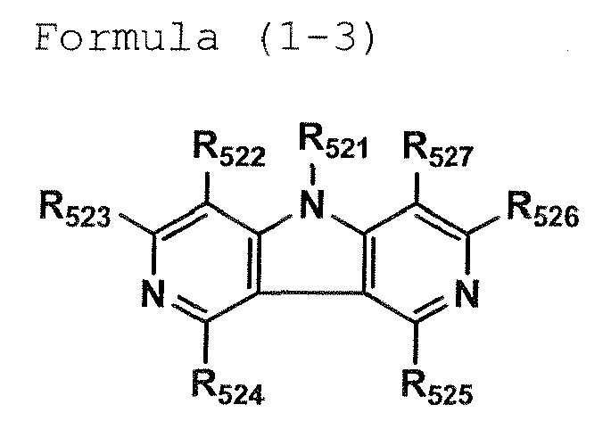
wherein R521 - R527 each independently represents a hydrogen atom or a substituent. - (9) The organic electroluminescent element of any one of Items 1 to 5, wherein the compound represented by Formula (1) is further represented by Formula (1-4).

wherein R531 - R537 each independently represents a hydrogen atom or a substituent. - (10) The organic electroluminescent element of any one of Items 1 to 5, wherein the compound represented by Formula (1) is further represented by Formula (1-5).
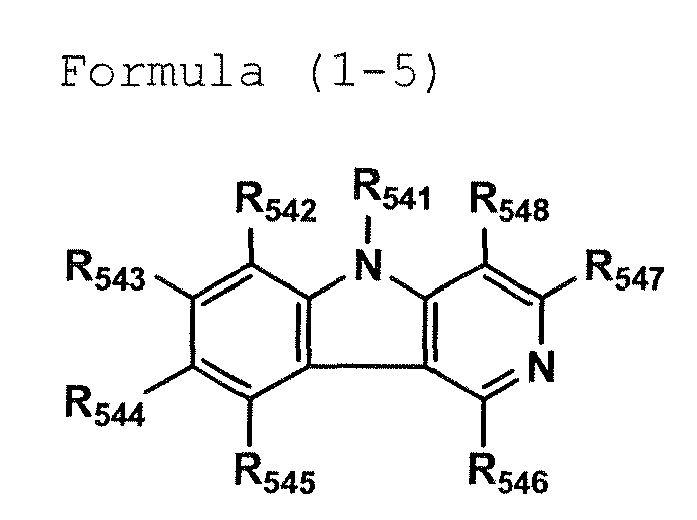
wherein R541 - R548 each independently represents a hydrogen atom or a substituent. - (11) The organic electroluminescent element of any one of Items 1 to 5, wherein the compound represented by Formula (1) is further represented by Formula (1-6).

wherein R551 - R558 each independently represents a hydrogen atom or a substituent. - (12) The organic electroluminescent element of any one of Items 1 to 5, wherein the compound represented by Formula (1) is further represented by Formula (1-7).

wherein R561 - R567 each independently represents a hydrogen atom or a substituent. - (13) The organic electroluminescent element of any one of Items 1 to 5, wherein the compound represented by Formula (1) is further represented by Formula (1-8).

wherein R571 - R577 each independently represents a hydrogen atom or a substituent. - (14) The organic electroluminescent element of any one of Items 1 to 5, wherein the compound represented by Formula (1) is further represented by Formula (1-9).
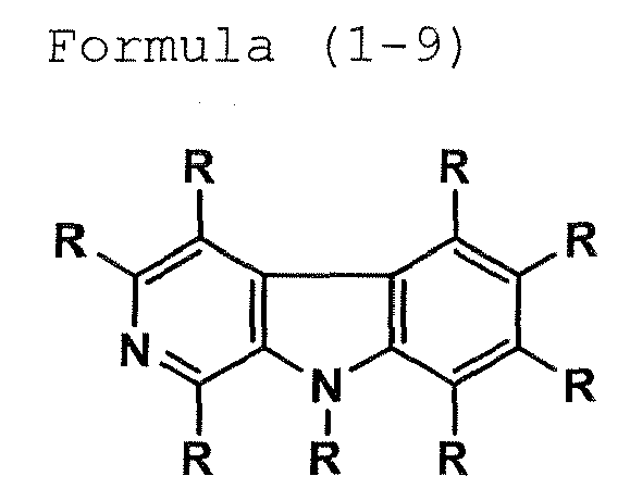
wherein each R represents a hydrogen atom or a substituent and a plurality of R may be the same or may be different from each other. - (15) The organic electroluminescent element of any one of Items 1 to 5, wherein the compound represented by Formula (1) is further represented by Formula (1-10).

wherein each R represents a hydrogen atom or a substituent and a plurality of R may be the same or may be different from each other. - (16) The organic electroluminescent element of any one of Items 1 to 5, wherein the compound represented by Formula (1) has at least one of groups represented by Formulae (2-1) to (2-8).


wherein- (a) in Formula (2-1), R502 - R507 each independently represents a hydrogen atom or a substituent;
- (b) in Formula (2-2), R512 - R517 each independently represents a hydrogen atom or a substituent;
- (c) in Formula (2-3), R522 - R527 each independently represents a hydrogen atom or a substituent;
- (d) in Formula (2-4), R532 - R537 each independently represents a hydrogen atom or a substituent;
- (e) in Formula (2-5), R542 - R548 each independently represents a hydrogen atom or a substituent;
- (f) in Formula (2-6), R552 - R558 each independently represents a hydrogen atom or a substituent;
- (g) in Formula (2-7), R562 - R567 each independently represents a hydrogen atom or a substituent; and
- (h) in Formula (2-8), R572 - R577 each independently represents a hydrogen atom or a substituent.
- (17) The organic electroluminescent element of any one of Items 1 to 5, wherein the compound represented by Formula (1) is further represented by Formula (3).

wherein R601 - R606 each independently represents a hydrogen atom or a substituent and at least one of R601 - R606 is represented by one of Formulae (2-1) to (2-4). - (18) The organic electroluminescent element of any one of Items 1 to 5, wherein the compound represented by Formula (1) is further represented by Formula (4).

wherein R611 - R620 each independently represents a hydrogen atom or a substituent and at least one of R611 - R620 is represented by one of Formulae (2-1) to (2-4). - (19) The organic electroluminescent element of any one of Items 1 to 5, wherein the compound represented by Formula (1) is further represented by Formula (5).

wherein R621 - R623 each independently represents a hydrogen atom or a substituent and at least one of R621 - R623 is represented by one of Formulae (2-1) to (2-4). - (20) The organic electroluminescent element of any one of Items 1 to 5, wherein the compound represented by Formula (1) is further represented by Formula (6).

wherein R631 - R645 each independently represents a hydrogen atom or a substituent and at least one of R631 - R645 is represented by one of Formulae (2-1) to (2-4). - (21) The organic electroluminescent element of any one of Items 1 to 5, wherein the compound represented by Formula (1) is further represented by Formula (7).

wherein R651 - R656 each independently represents a hydrogen atom or a substituent and at least one of R651 - R656 is represented by one of Formulae (2-1) to (2-4); na represents an integer of 0 to 5; and nb represents an integer of 1 to 6, provided that a sum of na and nb is 6. - (22) The organic electroluminescent element of any one of Items 1 to 5, wherein the compound represented by Formula (1) is further represented by Formula (8).

wherein R661 - R672 each independently represents a hydrogen atom or a substituent and at least one of R661 - R672 is represented by one of Formulae (2-1) to (2-4). - (23) The organic electroluminescent element of any one of Items 1 to 5, wherein the compound represented by Formula (1) is further represented by Formula (9).

wherein R681 - R688 each independently represents a hydrogen atom or a substituent and at least one of R681 - R688 is represented by one of Formulae (2-1) to (2-4). - (24) The organic electroluminescent element of any one of Items 1 to 5, wherein the compound represented by Formula (1) is further represented by Formula (10).

wherein R691 - R700 each independently represents a hydrogen atom or a substituent and at least one of R691 - R700 is represented by one of Formulae (2-1) to (2-4); and L1 represents a divalent linking group. - (25) The organic electroluminescent element of any one of Items 1 to 5, wherein the compound represented by Formula (1) is further represented by Formula (11).

wherein R1 and R2 each independently represents a hydrogen atom or a substituent; n and m each represents an integer of 1 to 2; and k and 1 each represents an integer of 3 to 4, provided that n + k = 5 and 1 + m = 5. - (26) The organic electroluminescent element of any one of Items 1 to 5, wherein the compound represented by Formula (1) is further represented by Formula (12).

wherein R1 and R2 each independently represents a hydrogen atom or a substituent; n and m each represents an integer of 1 to 2; and k and 1 each represents an integer of 3 to 4, provided that n + k = 5 and l + m = 5. - (27) The organic electroluminescent element of any one of Items 1 to 5, wherein the compound represented by Formula (1) is further represented by Formula (13).
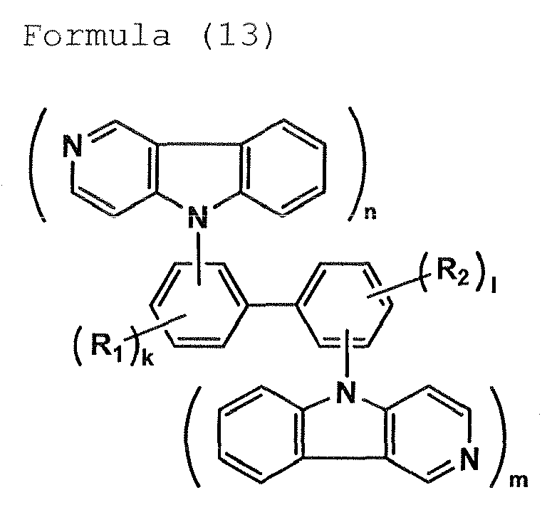
wherein R1 and R2 each independently represents a hydrogen atom or a substituent; n and m each represents an integer of 1 to 2; and k and 1 each represents an integer of 3 to 4, provided that n + k = 5 and 1 + m = 5. - (28) The organic electroluminescent element of any one of Items 1 to 5, wherein the compound represented by Formula (1) is further represented by Formula (14).

wherein R1 and R2 each independently represents a hydrogen atom or a substituent; n and m each represents an integer of 1 to 2; and k and 1 each represents an integer of 3 to 4, provided that n + k = 5 and l + m = 5. - (29) The organic electroluminescent element of any one of Items 1 to 5, wherein the compound represented by Formula (1) is further represented by Formula (15).
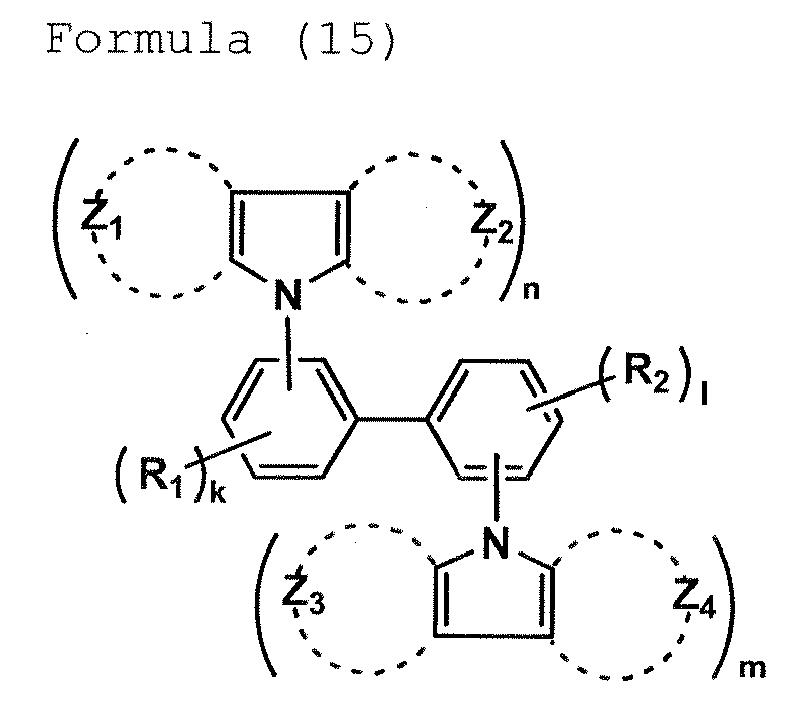
wherein R1 and R2 each independently represents a hydrogen atom or a substituent; n and m each represents an integer of 1 to 2; k and l each represents an integer of 3 to 4, provided that n + k = 5 and l + m = 5; and Z1, Z2, Z3 and Z4 each represent a 6-membered aromatic heterocyclic ring containing a nitrogen atom. - (30) The organic electroluminescent element of any one of Items 1 to 5, wherein the compound represented by Formula (1) is further represented by Formula (16).

wherein o and p each represents an integer of 1 to 3; Ar1 and Ar2 each represents an arylene group or a divalent aromatic heterocyclic group; Z1 and Z2 each represents a 6-membered aromatic heterocyclic ring containing a nitrogen atom; and L represents a divalent linking group. - (31) The organic electroluminescent element of any one of Items 1 to 5, wherein the compound represented by Formula (1) is further represented by Formula (17).

wherein o and p each represents an integer of 1 to 3; Ar1 and Ar2 each represents an arylene group or a divalent aromatic heterocyclic group; Z1, Z2, Z3 and Z4 each represents a 6-membered aromatic heterocyclic ring containing a nitrogen atom; and L represents a divalent linking group. - (32) The organic electroluminescent element of any one of Items 1 to 31, wherein the light emitting layer contains the compound represented by Formula (1).
- (33) The organic electroluminescent element of any one of Items 1 to 32, wherein at least one of the constituting layers is a hole blocking layer and the hole blocking layer contains the compound represented by Formula (1).
- (34) The organic electroluminescent element of any one of Items 1 to 33 which emits blue light.
- (35) The organic electroluminescent element of any one of Items 1 to 33 which emits white light.
- (36) A display device having the organic electroluminescent element of any one of Items 1 to 35.
- (37) An organic electroluminescent element comprising a pair of electrodes having therebetween at least one constituting layer containing a phosphorescent light emitting layer, wherein one of the constituting layer contains a compound represented by Formula (1-11):

wherein Z1 represents an aromatic heterocylic ring which may have a substituent; Z2 represents an aromatic heterocylic ring which may have a substituent or an aromatic hydrocarbon ring which may have a substituent; Z3 represents a divalent linking group or a single bond; L represents a divalent linking group; and the two groups linked by L may be the same or different from each other. - (38) The organic electroluminescent element of Item 37, wherein Z1 of the compound represented by Formula (1-11) is a 6-membered ring.
- (39) The organic electroluminescent element of Item 37 or Item 38, wherein Z2 of the compound represented by Formula (1-11) is a 6-membered ring.
- (40) The organic electroluminescent element of any one of Items 37 to 39, wherein Z3 of the compound represented by Formula (1-11) is a single bond.
- (41) The organic electroluminescent element of any one of Items 37 to 40, wherein the compound represented by Formula (1-11) has a molecular weight of 450 or more.
- (42) The organic electroluminescent element of any one of Items 37 to 41, wherein the light emitting layer contains the compound represented by Formula (1-11).
- (43) The organic electroluminescent element of any one of Items 37 to 42, wherein at least one of the constituting layers is a hole blocking layer and the hole blocking layer contains the compound represented by Formula (1-11).
- (44) The organic electroluminescent element of any one of Items 37 to 43 which emits blue light.
- (45) The organic electroluminescent element of any one of Items 37 to 43 which emits white light.
- (46) A display device having the organic electroluminescent element of any one of Items 37 to 45.
- (47) An organic electroluminescent element comprising a pair of electrodes having therebetween at least one constituting layer containing a phosphorescent light emitting layer, wherein one of the constituting layer contains a compound represented by Formula (1-12):

wherein R102 represents an alkyl group which may have a substituent, a cycloalkyl group which may have a substituent, an aryl group which may have a substituent or a heterocyclic group which may have a substituent; Z4 and Z5 each independently represents an atom group which is necessary to form a 5 - 7 membered heterocylic ring containing nitrogen; and Z3 represents a divalent linking group or a single bond. - (48) The organic electroluminescent element of Item 47, wherein Z3 of the compound represented by Formula (1-12) is a single bond.
- (49) The organic electroluminescent element of Item 47 or Item 48, wherein the compound represented by Formula (1-12) has a molecular weight of 450 or more.
- (50) The organic electroluminescent element of any one of Items 47 to 49, wherein the light emitting layer contains the compound represented by Formula (1-12).
- (51) The organic electroluminescent element of any one of Items 47 to 50, wherein at least one of the constituting layers is a hole blocking layer and the hole blocking layer contains the compound represented by Formula (1-12).
- (52) The organic electroluminescent element of any one of Items 47 to 51 which emits blue light.
- (53) The organic electroluminescent element of any one of Items 47 to 51 which emits white light.
- (54) A display device having the organic electroluminescent element of any one of Items 47 to 53.
- (55) An organic electroluminescent element comprising a pair of electrodes having therebetween at least one constituting layer containing a phosphorescent light emitting layer, wherein one of the constituting layer contains a compound represented by Formula (1-13):

wherein R103 represents an alkyl group which may have a substituent, a cycloalkyl group which may have a substituent, an aryl group which may have a substituent or a heterocyclic group which may have a substituent; R104 represents a hydrogen atom or a substituent; and Z6 and Z7 each independently represents an atom group which is necessary to form a 5 - 7 membered heterocylic ring containing nitrogen. - (56) The organic electroluminescent element of Item 55, wherein Z6 of the compound represented by Formula (1-13) is a 6-membered ring.
- (57) The organic electroluminescent element of Item 55 or Item 56, wherein Z7 of the compound represented by Formula (1-13) is a 6-membered ring.
- (58) The organic electroluminescent element of any one of Items 55 to 57, wherein the compound represented by Formula (1-13) has a molecular weight of 450 or more.
- (59) The organic electroluminescent element of any one of Items 55 to 58, wherein the light emitting layer contains the compound represented by Formula (1-13).
- (60) The organic electroluminescent element of any one of Items 55 to 59, wherein at least one of the constituting layers is a hole blocking layer and the hole blocking layer contains the compound represented by Formula (1-13).
- (61) The organic electroluminescent element of any one of Items 55 to 60 which emits blue light.
- (62) The organic electroluminescent element of any one of Items 55 to 60 which emits white light.
- (63) A display device having the organic electroluminescent element of any one of Items 55 to 62.
-
- Fig. 1 is a schematic drawing of one example of a display comprising an organic EL element.
- Fig. 2 is a schematic drawing of a display section.
- Fig. 3 is a schematic drawing of a pixel.
- Fig. 4 is a schematic drawing of a display employing a passive matrix method.
- Details of the constituting elements of the present invention will now be explained.
- Compounds used in the present invention will be explained.
- Compounds represented by Formula (1) will be explained.
- An organic EL element employing a compound represented by Formula (1) was found to exhibit high emission efficiency. Further, an organic EL element employing a compound represented by Formula (1) was found to exhibit a long life.
- In Formula (1), Z1 represents an aromatic heterocylic ring which may have a substituent; Z2 represents an aromatic heterocylic ring which may have a substituent or an aromatic hydrocarbon ring which may have a substituent; Z3 represents a divalent linking group or a single bond; and R101 represents a hydrogen atom or a substituent.
- In Formula (1), examples of an aromatic heterocyclic ring represented by Z1 or Z2 include: a furan ring, a thiophene ring, a pyridine ring, a pyridazine ring, a pyrimidine ring, a pyrazine ring, a triazine ring, a benzimidazole ring, an oxadiazole ring, a triazole ring, an imidazole ring, a pyrazole ring, a thiazole ring, an indole ring, a benzimidazole ring, a benzothiazole ring, a benzoxazole ring, a quinoxaline ring, a quinazoline ring, a phthalazine ring, a carbazole ring, a carboline ring and a ring which is formed by replacing one of the carbon atoms of a hydrocarbon ring constituting a carboline ring with a nitrogen atom. The above mentioned aromatic hydrocarbon rings may have a substituent represented by R101 which will be described later.
- In Formula (1), examples of an aromatic hydrocarbon ring represented by Z2 include: a benzene ring, a biphenyl ring, a naphthalene ring, an azulene ring, an anthracene ring, a phenanthrene ring, a pyrene ring, a chrysene ring, a naphthacene ring, a triphenylene ring, o-terphenyl ring, m-terphenyl ring, a p-terphenyl ring, an acenaphthene ring, a coronene ring, a fluorene ring, a fluoranthrene ring, a naphthacene ring, a pentacene ring, a perylene ring, a pentaphene ring, a picene ring, a pyrene ring, a pyranthrene ring and a anthranthrene ring. Furthermore, the above mentioned aromatic hydrocarbon rings may have a substituent represented by R101 which will be described below.
- In Formula (1), examples of a substitute represented by R101 include: alkyl groups (for example, a methyl group, an ethyl group, a propyl group, an isopropyl group, a tert-butyl group, a pentyl group, a hexyl group, an octyl group, a dodecyl group, a tridecyl group, a tetradecyl group and a pentadecyl group); cycloalkyl groups (for example, a cyclopentyl group and a cyclohexyl group); alkenyl groups (for example, a vinyl group and an allyl group); alkynyl groups (for example, an ethynyl group and a propargyl group); aryl groups (for example, a phenyl group and a naphthyl group); aromatic heterocyclic groups (for example, a furyl group, a thienyl group, a pyridyl group, a pyridazinyl group, a pyrimidinyl group, a pyrazinyl group, the triazinyl group, an imidazolyl group, a pyrazolyl group, a thiazolyl group, a quinazolinyl group and a phthalazinyl group), heterocyclic groups (for example, a pyrrolidyl group, an imidazolidyl group, a morpholyl group and an oxazolidyl group), alkoxyl groups (for example, a methoxy group, an ethoxy group, a propyloxy group, a pentyloxy group, a hexyloxy group, an octyloxy group and a dodecyloxy group), cyclo alkoxyl groups (for example, a cyclopentyloxy group, a cyclohexyloxy group), aryloxy groups (for example, a phenoxy group and a naphthyloxy group), alkylthio groups (for example, a methylthio group, an ethylthio group, a propylthio group, a pentylthio group, a hexylthio group, an octylthio group and a dodecylthio group), cycloalkylthio groups (for example, a cyclopentylthio group and a cyclohexylthio group), arylthio groups (for example, a phenylthio group and a naphthylthio group), alkoxycarbonyl groups (for example, a methyloxycarbonyl group, an ethyloxycarbonyl group, a butyloxycarbonyl group, an octyloxycarbonyl group and a dodecyloxycarbonyl group), aryloxycarbonyl groups (for example, a phenyloxycarbonyl group and a naphthyloxycarbonyl group), sulfamoyl groups (for example, the aminosulfonyl group, a methylaminosulfonyl group, a dimethylaminosulfonyl group, a butylaminosulfonyl group, a hexylaminosulfonyl group, a cyclohexylaminosulfonyl group, an octylaminosulfonyl group, a dodecylaminosulfonyl group, a phenylaminosulfonyl group, a naphthylaminosulfonyl group and 2-pyridylaminosulfonyl group), acyl groups (for example, an acetyl group, an ethylcarbonyl group, a propylcarbonyl group, a pentylcarbonyl group, a cyclohexylcarbonyl group, an octylcarbonyl group, 2-ethylhexylcarbonyl group, a dodecylcarbonyl group, a phenylcarbonyl group, a naphthylcarbonyl group and a pyridyl carbonylgroup), acyloxy groups (for example, an acetyloxy group, an ethylcarbonyloxy group, a butylcarbonyloxy group, an octylcarbonyloxy group, a dodecylcarbonyloxy group and a phenylcarbonyloxy group), amide groups (for example, a methylcarbonylamino group, an ethylcarbonylamino group, a dimethylcarbonylamino group, a propylcarbonylamino group, a pentylcarbonylamino group, a cyclohexylcarbonylamino group, 2-ethylhexylcarbonylamino group, an octylcarbonylamino group, a dodecylcarbonylamino group, a phenylcarbonylamino group, a naphthylcarbonylamino group, etc.), carbamoyl groups (for example, the aminocarbonyl group, a methylaminocarbonyl group, a dimethylaminocarbonyl group, a propylaminocarbonyl group, a pentylaminocarbonyl group, a cyclohexylaminocarbonyl group, an octylaminocarbonyl group, 2-ethylhexylaminocarbonyl group, a dodecylaminocarbonyl group, a phenylaminocarbonyl group, a naphthylaminocarbonyl group and 2-pyridylaminocarbonyl group), ureido groups (for example, a methylureido group, an ethylureido group, a pentylureido group, a cyclohexylureido group, an octylureido group, a dodecylureidc group, a phenylureido group naphthylureido group and 2-pyridylaminoureido group), sulfinyl groups (for example, a methylsulfinyl group, an ethylsulfinyl group, a butylsulfinyl group, a cyclohexylsulfinyl group, 2-ethylhexylsulfinyl group, a dodecylsulfinyl group, a phenylsulfinyl group, a naphthylsulfinyl group and 2-pyridylsulfinyl group), alkylsulfonyl groups (for example, a methylsultonylamino group, an ethylsulfonyl group, a butylsulfonyl group, a cyclohexylsulfonyl group, 2-ethylhexylsulfonyl group and a dodecylsulfonyl group), arylsulfonyl groups (a phenylsulfonyl group, a naphthylsulfonyl group and 2-pyridylsulfonyl group), amino groups (for example, an amino group, an ethylamino group, a dimethylamino group, a butylamino group, a cyclopentylamino group, 2-ethylhexylamino group, a dodecylamino group, an anilino group and a naphthylamino group, 2-pyridylamino group), halogen atoms (for example, a fluorine atom, a chlorine atom and a bromine atom), fluoride hydro fluoro carbon groups (for example, a fluoromethyl group, a trifluoromethyl group, a pentafluoroethyl group and a pentafluorophenyl group), a cyano group, a nitro group, a hydroxy group, a mercapto group, silyl groups (for example, a trimethylsilyl group, a triisopropylsilyl group, a triphenylsilyl group and a phenyldiethylsilyl group).
- These substituents may further be replaced by another substituent described above. Moreover, a plurality of substituents may be combined together to form a ring.
- The preferable substituents include an alkyl group, a cycloalkyl group, a hydro fluoro carbon group, an aryl group and an aromatic heterocyclic group.
- Examples of a divalent linking group may include hydrocarbon groups such as an alkylene group, an alkenylene group, an alkynylene and an arylene group; a group containing a heteroatom; divalent linking groups derived from a compound containing aromatic heterocyclic ring (also referred to as a heteroaromatic compound) such as a thiophene-2,5-diyl group and a pyrazine-2,3-diyl group; chalcogen atoms such as an oxygen atom and a sulfur atom; and linking groups containing a linkage through a heteroatom such as an alkylimino group, a dialkylsilanediyl group and a diarylgermanediyl group.
- A single bond represents a bond directly combining two substituents.
- In the present invention, Z1 in Formula (1) is preferably a 6-membered ring, whereby high emission efficiency is obtained and, further, a longer life is attained.
- In the present invention, Z2 in Formula (1) is preferably a 6-membered ring, whereby high emission efficiency is obtained and, further, a longer life is attained.
- Further, both of Z1 and Z2 in Formula (1) are preferably 6-membered rings, whereby a still longer life is attained.
- Among the compounds represented by Formula (1), preferable are the compounds represented by Formulae (1-1) to (1-13).
- In Formula (1-1), R501 - R507 each independently represents a hydrogen atom or a substituent.
- By using a compound represented by Formula (1-1), an organic EL element exhibiting higher emission efficiency and, further, a longer life is obtained.
- In Formula (1-2), R511 - R517 each independently represents a hydrogen atom or a substituent.
- By using a compound represented by Formula (1-2), an organic EL element exhibiting higher emission efficiency and, further, a longer life is obtained.
- In Formula (1-3), R521 - R527 each independently represents a hydrogen atom or a substituent.
- By using a compound represented by Formula (1-3), an organic EL element exhibiting higher emission efficiency and, further, a longer life is obtained.
- In Formula (1-4), R531 - R537 each independently represents a hydrogen atom or a substituent.
- By using a compound represented by Formula (1-4), an organic EL element exhibiting higher emission efficiency and, further, a longer life is obtained.
- In Formula (1-5), R541 - R548 each independently represents a hydrogen atom or a substituent.
- By using a compound represented by Formula (1-5), an organic EL element exhibiting higher emission efficiency and, further, a longer life is obtained.
- In Formula (1-6), R551 - R558 each independently represents a hydrogen atom or a substituent.
- By using a compound represented by Formula (1-6), an organic EL element exhibiting higher emission efficiency and, further, a longer life is obtained.
- In Formula (1-7), R561 - R567 each independently represents a hydrogen atom or a substituent.
- By using a compound represented by Formula (1-7), an organic EL element exhibiting higher emission efficiency and, further, a longer life is obtained.
- In Formula (1-8), R571 - R577 each independently represents a hydrogen atom or a substituent.
- By using a compound represented by Formula (1-8), an organic EL element exhibiting higher emission efficiency and, further, a longer life is obtained.
- In Formula (1-9), R represents a hydrogen atom or a substituent. A plurality of R may be the same or may be different from each other
- By using a compound represented by Formula (1-9), an organic EL element exhibiting higher emission efficiency and, further, a longer life is obtained.
- In Formula (1-10), R represents a hydrogen atom or a substituent. A plurality of R may be the same or may be different from each other.
- By using a compound represented by Formula (1-10), an organic EL element exhibiting higher emission efficiency and, further, a longer life is obtained.
- In Formula (1-11), Z1 represents an aromatic heterocylic ring which may have a substituent; Z2 represents an aromatic heterocylic ring which may have a substituent or an aromatic hydrocarbon ring which may have a substituent; Z3 represents a divalent linking group or a single bond. L represents a divalent linking group. Two groups linked by L may be the same or may be different from each other.
- By using a compound represented by Formula (1-11), an organic EL element exhibiting higher emission efficiency and, further, a longer life is obtained.
- In Formula (1-12), R102 represents an alkyl group which may have a substituent, a cycloalkyl group which may have a substituent, an aryl group which may have a substituent or a heterocyclic group which may have a substituent; Z4 and Z5 each independently represents an atom group which is necessary to form a 5 - 7 membered heterocylic ring containing nitrogen; and Z3 represents a divalent linking group or a single bond.
- By using a compound represented by Formula (1-12), an organic EL element exhibiting higher emission efficiency and, further, a longer life is obtained.
- In Formula (1-13), R103 represents an alkyl group which may have a substituent, a cycloalkyl group which may have a substituent, an aryl group which may have a substituent or a heterocyclic group which may have a substituent; R104 represents a hydrogen atom or a substituent; and Z6 and Z7 each represents an atom group which is necessary to form a 5 - 7 membered ring.
- By using a compound represented by Formula (1-13), an organic EL element exhibiting higher emission efficiency and, further, a longer life is obtained.
- The substituents which may further be introduced in each of Formulae (1-1) to (1-13) are common to the substituents represented by R101 in the compound represented by Formula (1).
- Among the compounds represented by Formula (1), preferable are the compounds containing at least one group represented by any one of Formulae (2-1) to (2-8). Specifically preferable are the compounds having 2 to 4 groups represented by Formulae (2-1) to (2-2) a molecule, in which also included is the case when only the portions except for R101 of the structure represented by Formula (1) are replaced by the groups represented by Formulae (2-1) to (2-8).
- Herein, the compounds represented by Formulae (3) to (17) are preferable to obtain the effect of the present invention.
- In Formula (3), R601 - R606 each independently represents a hydrogen atom or a substituent and at least one of R601 - R606 is represented by one of Formulae (2-1) to (2-4).
- By using a compound represented by Formula (3), an organic EL element exhibiting higher emission efficiency and, further, a longer life is obtained.
- In Formula (4), R611- R620 each independently represents a hydrogen atom or a substituent and at least one of R611 - R620 is represented by one of Formulae (2-1) to (2-4).
- By using a compound represented by Formula (4), an organic EL element exhibiting higher emission efficiency and, further, a longer life is obtained.
- In Formula (5), R621 - R623 each independently represents a hydrogen atom or a substituent and at least one of R621 - R623 is represented by one of Formulae (2-1) to (2-4).
- By using a compound represented by Formula (5), an organic EL element exhibiting higher emission efficiency and, further, a longer life is obtained.
- In Formula (6), R631 - R645 each independently represents a hydrogen atom or a substituent and at least one of R631 - R645 is represented by one of Formulae (2-1) to (2-4).
- By using a compound represented by Formula (6), an organic EL element exhibiting higher emission efficiency and, further, a longer life is obtained.
- In Formula (7), R651 - R656 each independently represents a hydrogen atom or a substituent and at least one of R651 - R656 is represented by one of Formulae (2-1) to (2-4).
- By using a compound represented by Formula (7), an organic EL element exhibiting higher emission efficiency and, further, a longer life is obtained.
- In Formula (8), R661 - R672 each independently represents a hydrogen atom or a substituent and at least one of R661 - R672 is represented by one of Formulae (2-1) to (2-4).
- By using a compound represented by Formula (8), an organic EL element exhibiting higher emission efficiency and, further, a longer life is obtained.
- In Formula (9), R681 - R688 each independently represents a hydrogen atom or a substituent and at least one of R681 - R688 is represented by one of Formulae (2-1) to (2-4).
- By using a compound represented by Formula (9), an organic EL element exhibiting higher emission efficiency and, further, a longer life is obtained.
- In Formula (10), R691 - R700 each independently represents a hydrogen atom or a substituent and at least one of R691 - R700 is represented by one of Formulae (2-1) to (2-4).
- Examples of a divalent linking group represented by L1 in Formula (10) include: hydrocarbon groups, for example, alkylene groups (for example, an ethylene group, a trimethylene group, a tetramethylene group, a propylene group, an ethylethylene group, a pentamethylene group, a hexamethylene group, 2,2,4-trimethylhexamethylene group, a heptamethylene group, an octamethylene group, a nonamethylene group, a decamethylene group, an undecamethylene group, a dodecamethylene group, cyclohexylene groups (for example, a 1,6-cyclohexanediyl group), cyclopentylene groups (for example, a 1,5-cyclopentanediyl group), alkenylene groups (for example, a vinylene group and a propenylene group), alkynylene groups (for example, a ethynylene group and 3-pentynylene group, etc.), and arylene groups; and groups containing a hetero atom (for example, divalent groups containing a chalcogen atom, such as -O- and -S-; and -N(R)-groups where R represents a hydrogen atom or an alkyl group wherein the alkyl group is common to the alkyl groups represented by R101 in Formula (1)).
- In each of the above alkylene group, alkenylene group, and arylene group, at least one of the carbon atoms constituting the divalent group may be replaced by a chalcogen atom (oxygen or sulfur) or the -N(R)- group.
- Further, examples of a divalent linking group represented by L1 include: groups having a divalent heterocyclic group, for example, an oxazolediyl group, a pyrimidinediyl group, a pyridazinediyl group, a pyrandiyl group, a pyrrolinediyl group, an imidazolinediyl group, an imidazolidinediyl group, a pyrazolidinediyl group, a pyrazolinediyl group, a piperidinediyl group, a piperazinediyl group, a morpholinediyl group, and a quinuclidinediyl group; and divalent linking groups derived from compounds having an aromatic heterocyclic ring (also referred to as a heteroaromatic compounds), for example, a thiophene-2,5-diyl group and a pyrazine-2,3-diyl group.
- Also included are divalent linking groups containing a linkage via a hetero atom, for example, an alkylimino group, a dialkylsilanediyl group and a diarylgermanediyl group.
- By using a compound represented by Formula (10), an organic EL element exhibiting higher emission efficiency and, further, a longer life is obtained.
- In each compound represented by Formulae (11) to (15), the substituents represented by R1 and R2 are common to the substituents represented by R101 in Formula (1).
- Examples of a 6-membered aromatic heterocyclic ring containing at least one nitrogen atom which is represented by Z1, Z2, Z3 or Z4 of Formula (15) include: a pyridine ring, a pyridazine ring, a pyrimidine ring and a pyrazine ring.
- Examples of a 6-membered aromatic heterocyclic ring containing at least one nitrogen atom which is represented by Z1 or Z2 of Formula (16) include: a pyridine ring, a pyridazine ring, a pyrimidine ring and a pyrazine ring.
- Examples of an arylene group represented by Ar1 or Ar2 of Formula (16) include: an o-phenylene group, a m-phenylene group, a p-phenylene group, a naphthalenediyl group, an anthracenediyl group, a naphthacenediyl group, a pyrenediyl group, a naphthylnaphthalenediyl group, a biphenyldiyl groups (for example, a 3,3'-biphenyldiyl group and a 3,6-biphenyldiyl group), a terphenyldiyl group, a quaterphenyldiyl group, a kinkphenyldiyl group, the sexiphenyldiyl group, the septiphenyldiyl group, an octiphenyldiyl group, the noviphenyldiyl group and a deciphenyldiyl group. The above mentioned arylene group may further have a substituent which will be described later.
- Examples of a divalent aromatic heterocyclic group represented by Ar1 or Ar2 of Formula (16) include: a furan ring, a thiophene ring, a pyridine ring, a pyridazine ring, a pyrimidine ring, a pyrazine ring, a triazine ring, a benzimidazole ring, an oxadiazole ring, a triazole ring, an imidazole ring, a pyrazole ring, a thiazole ring, an indole ring, a benzimidazole ring, a benzothiazole ring, a benzoxazole ring, a quinoxaline ring, a quinazoline ring, a phthalazine ring, a carbazole ring, a carboline ring and a divalent group, for example, derived from a hydrocarbon ring constituting a carboline ring, of which a carbon atom is further replaced with a nitrogen atom. Further, the above mentioned aromatic heterocyclic group may have a substituent represented by R101.
- The divalent linking groups represented by L in Formula (16) are common to the divalent linking groups represented by L1 in Formula (10), however, preferable are an alkylene group or a divalent group containing a chalcogen atom, for example, -O- or -S-, and more preferable is an alkylene group.
- The arylene groups represented by Ar1 or Ar2 in Formula (17) are common to the arylene groups represented by Ar1 or Ar2 in Formula (16).
- Examples of the 6-membered aromatic heterocyclic ring containing at least one nitrogen atom represented by Z1, Z2, Z3 or Z4 in Formula (17) include: a pyridine ring, a pyridazine ring, a pyrimidine ring and a pyrazine ring.
- In the following, the compounds relating the poresent invention or specific examples of the compounds relating the present invention will be shown, however, the present invention is not limited thereto:
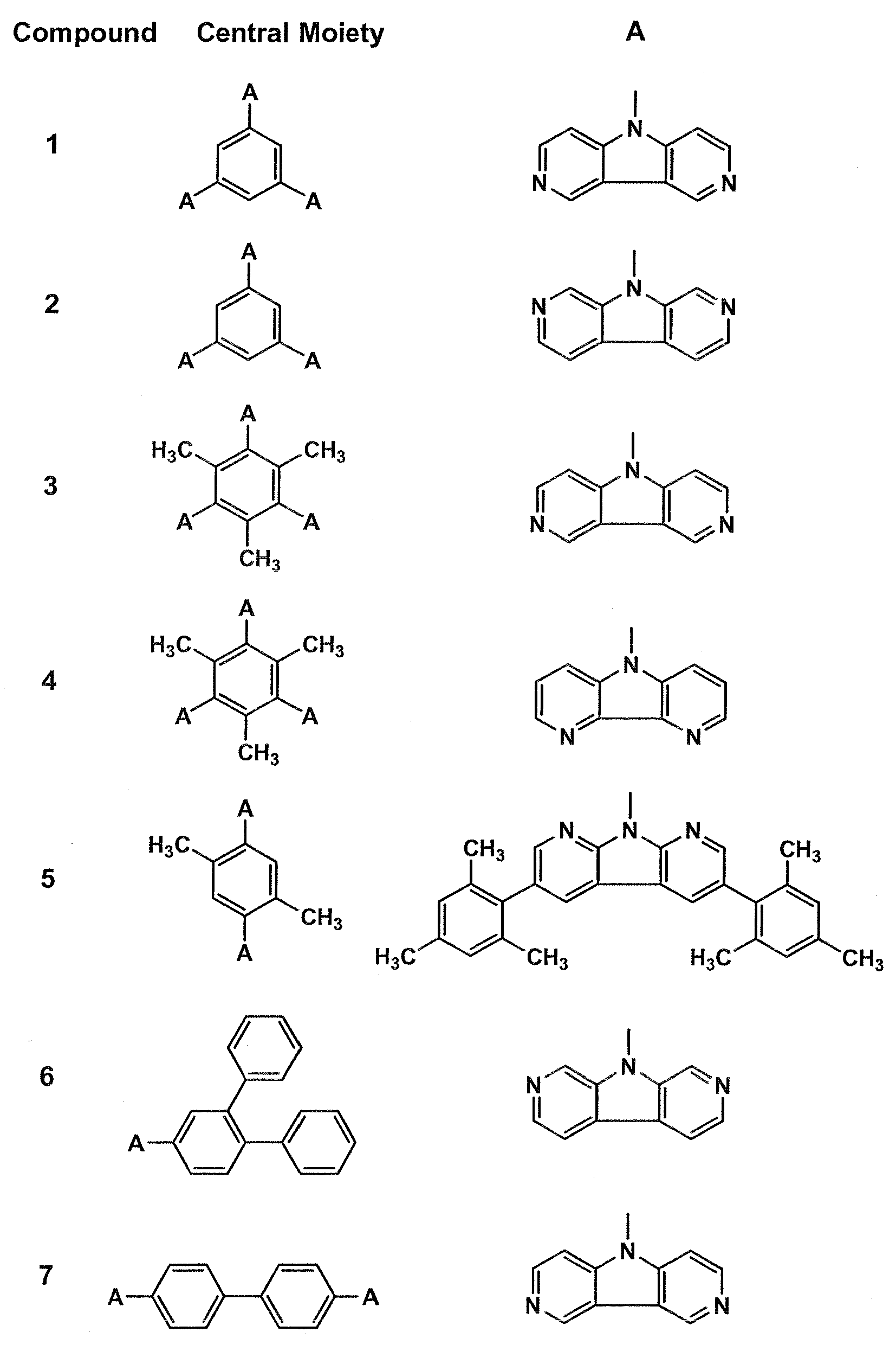


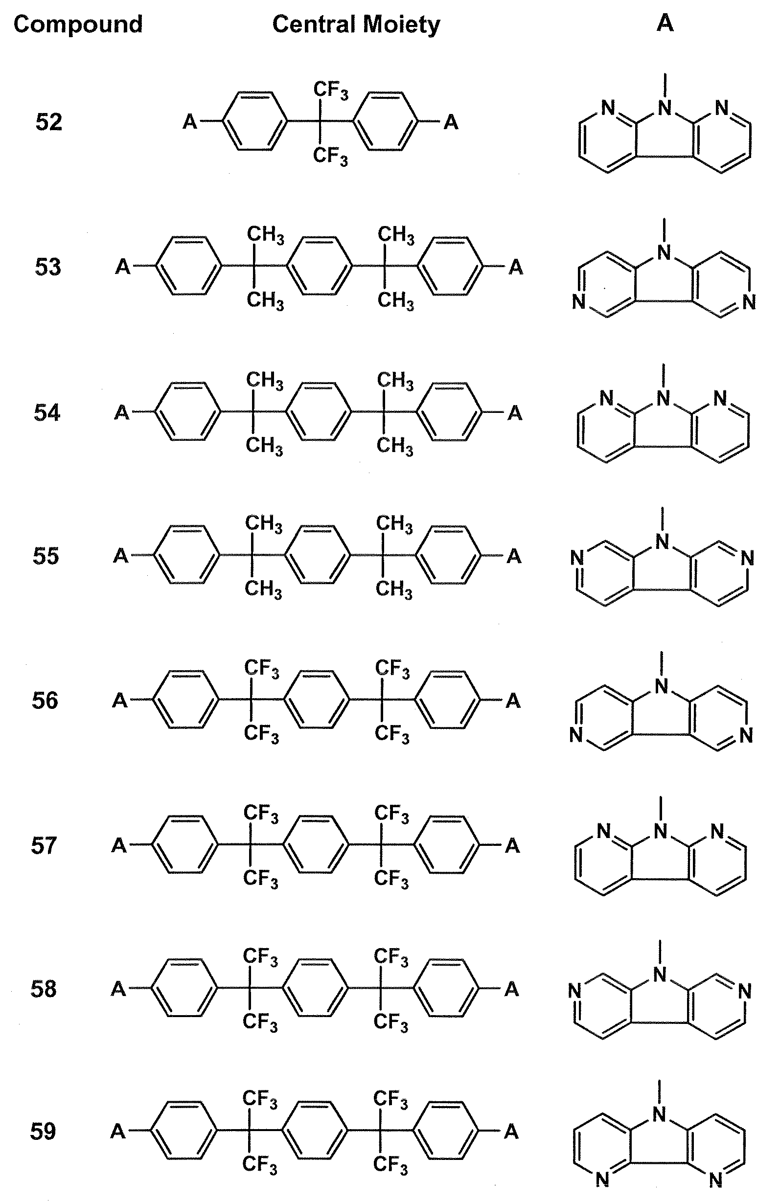


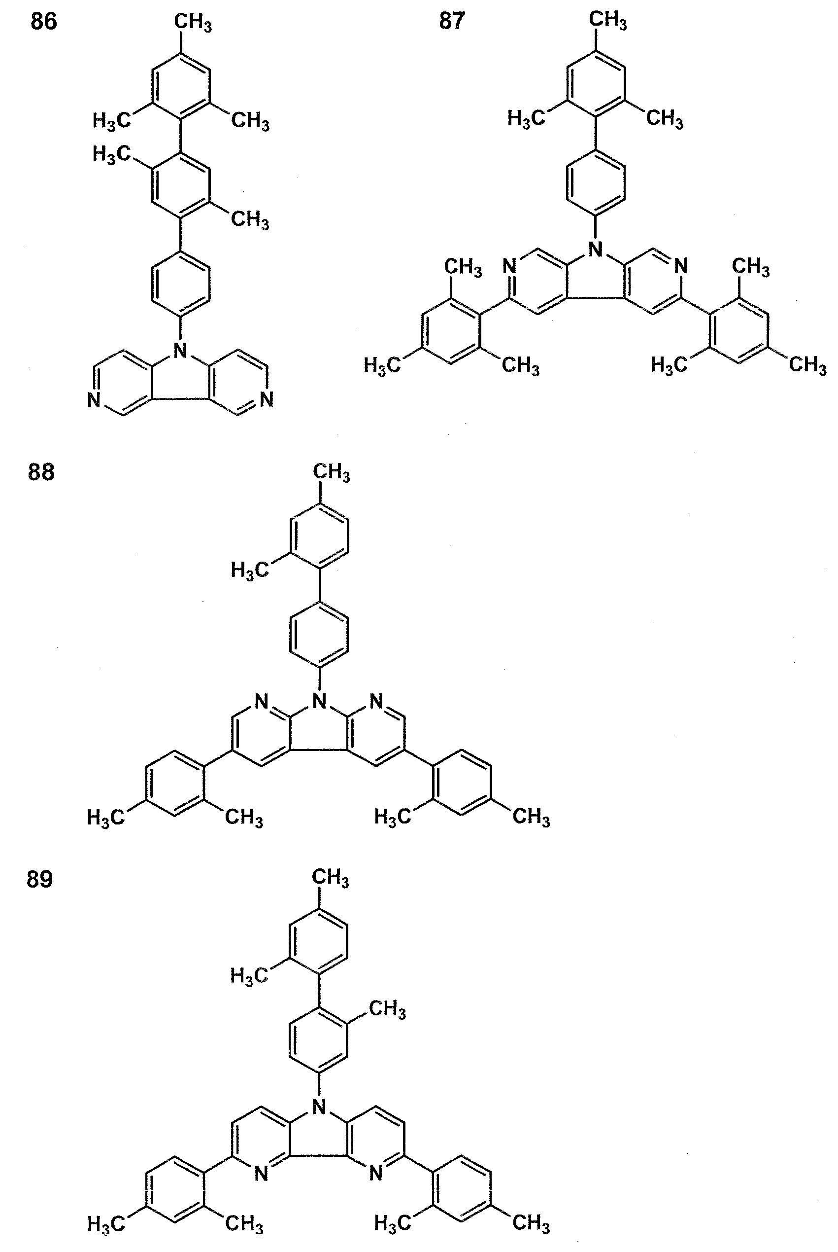

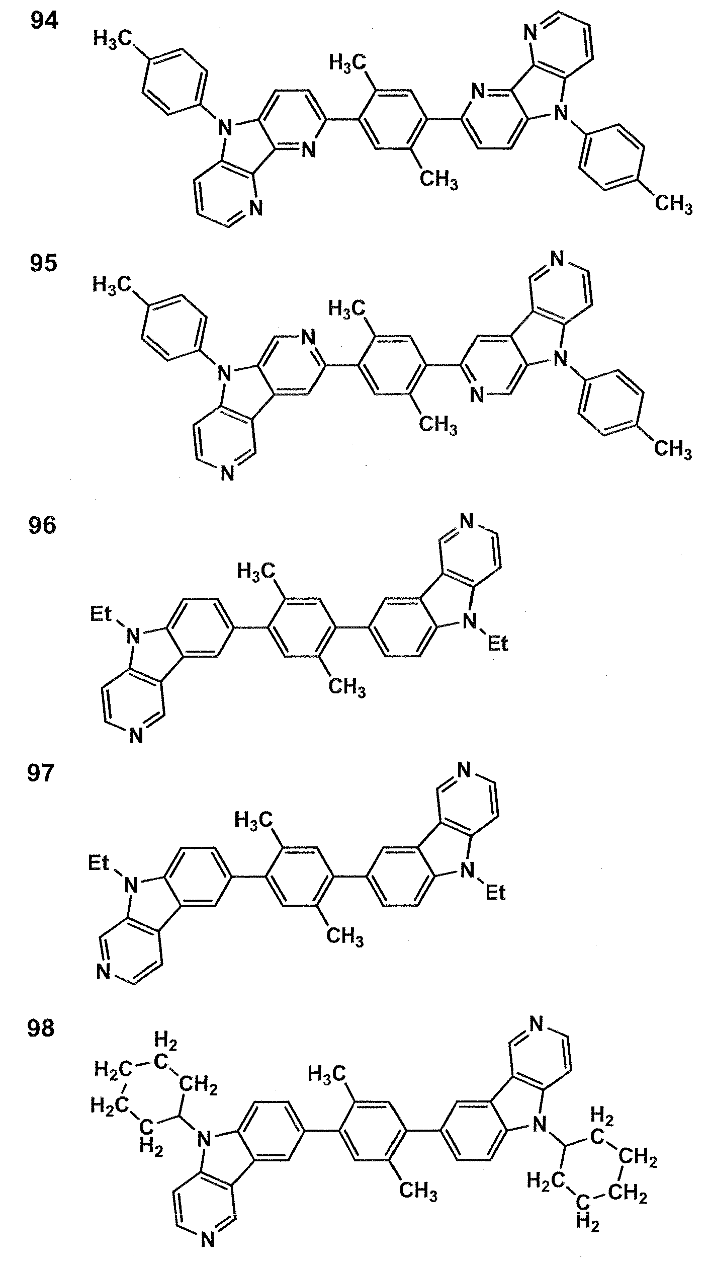
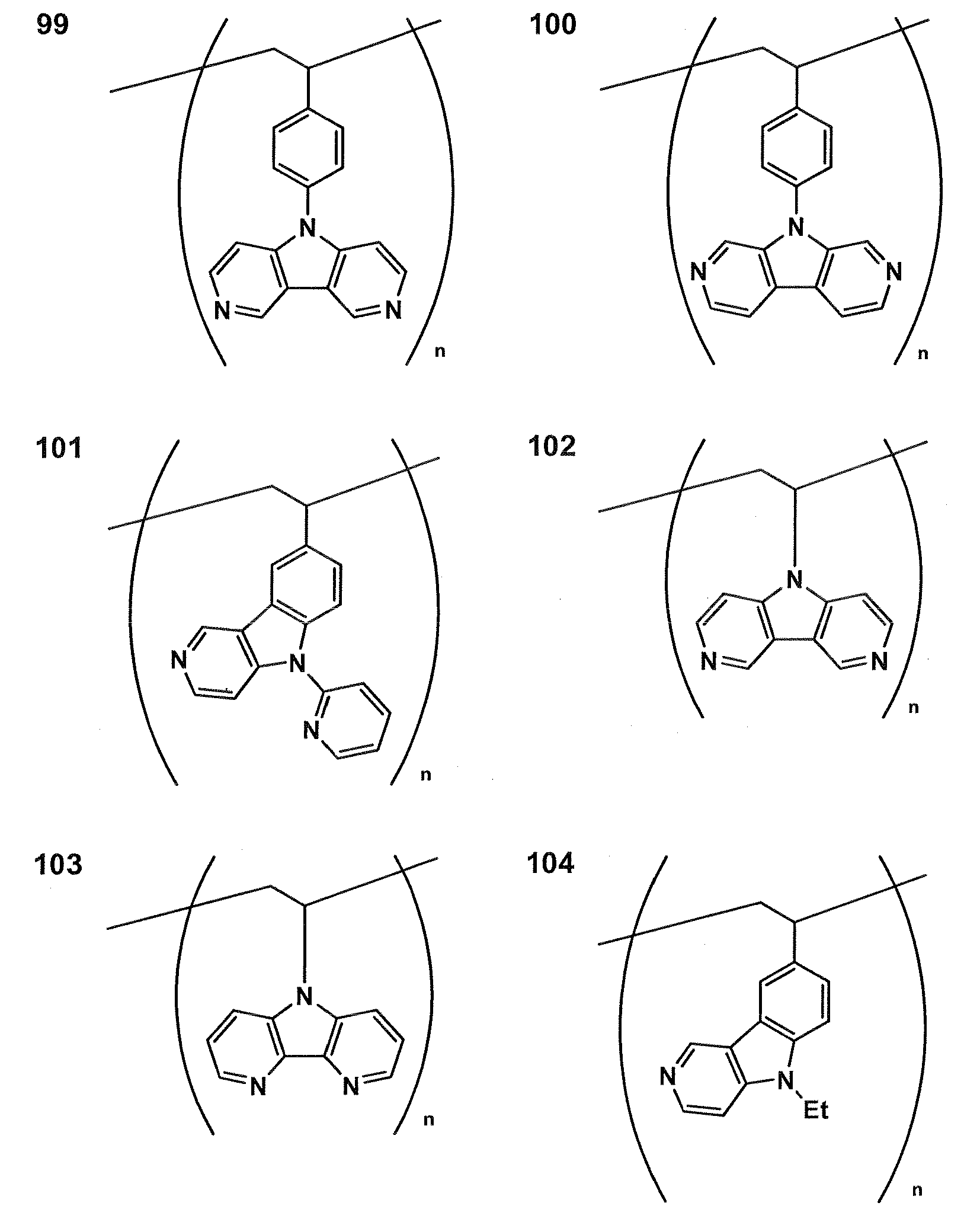


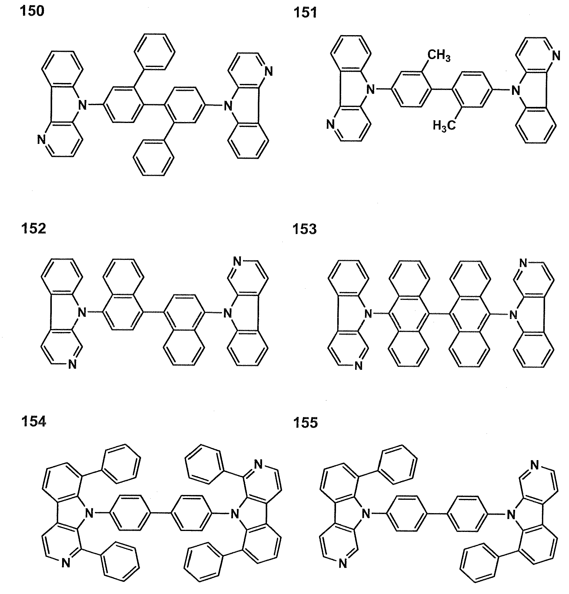


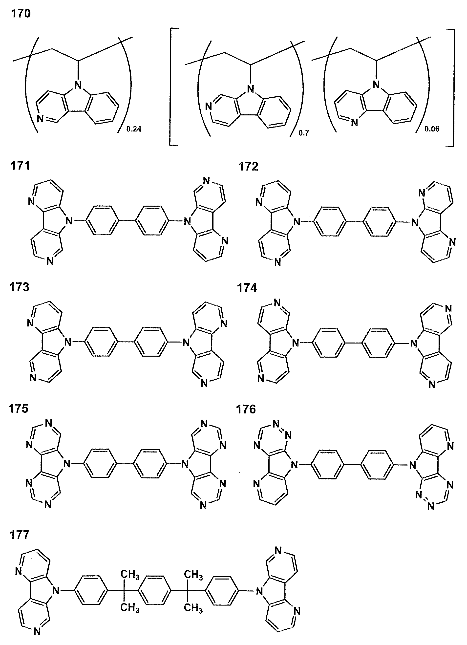


- In the following, typical compounds relating the present invention or typical examples of preparation method of the compounds relating the present invention will be described, however, the present invention is not limited thereto.
-

- In a mixed solution of 50 ml of N,N-dimethylacetamide, 6.87 g of 4,4'-diiodobiphenyl and 6.00 g of β-carboline, 4.5 g of copper powder and 7.36 g of potassium carbonate were added, and then heat reflux was carried out for 15 hours. After standing to cool, water and chloroform were added, and the insoluble portion was removed by filtering. Then, the organic layer was separated, washed by water and saturated sodium chloride solution, and condensed under reduced pressure. The obtained residue was dissolved in acetic acid, treated with activated carbon, and recrystallized to obtain 4.2g of colorless crystals of the exemplified compound 73.
- The structure of the exemplifying compound 73 was identified with 1H-NMR spectrum and mass spectroscopy analysis. The property data and spectrum data of the exemplified compound 73 are shown below.
- A colorless crystal, melting point: 200 °C
MS (FAB) m/z: 487 (M+1)
1H-NMR (400MHz, CDCl3) : δ/ppm 7.3-7.5 (m, 2H), 7.5-7.6 (m, 4H), 7.7-7.8 (m, 4H), 7.9-8.0 (m, 4H), 8.06 (d, J= 5.1Hz, 2H), 8.24 (d, J = 7.8Hz, 2H), 8.56 (d, J = 5.1Hz, 2H), 8.96 (s, 2H) -

- 0.32 g of palladium acetate and 1.17 g of tri-tert-butylphosphine were dissolved in 10 ml of anhydrous toluene and 50mg of sodium borohydride was further added. After the mixture was agitated for 10 minutes at room temperature, 5.00 g of δ-carboline, 5.87 g of 4,4'-diiodobiphenyl and 3.42 g of sodium-tert-butoxide were dispersed in 50 ml of anhydrous xylene, and agitated for 10 hours at the reflux temperature under a nitrogen atmosphere. After standing the reaction mixture to cool, chloroform and water were added, and the organic layer was separated. The organic layer was washed with water and a saturated sodium chloride solution, and condensed under reduced pressure. The obtained residue was dissolved in tetrahydrofuran, treated with activated carbon, and recrystallized to obtain 5.0 g of colorless crystals of the exemplified compound 74.
- The structure of the exemplifying compound 74 was identified with 1H-NMR spectrum and mass spectroscopy analysis. The property data and spectrum data of the exemplified compound 74 are shown below.
MS(FAB) m/z: 487(M+1)
1H-NMR (400MHz, CDCl3) : δ/ppm 7.37 (dd, J= 4.7Hz, J= 8.3Hz, 2H), 7.4 - 7.5 (m, 2H), 7.5 - 7.6 (m, 4H), 7.7 - 7.8 (m, 4H), 7.81 (dd, J = 1.2Hz, J= 8.3Hz, 2H), 7.9 - 8.0 (m, 4H), 8.48 (d, J = 7.8Hz, 2H), 8.65 (dd, J= 1.2Hz, J = 4.6Hz, 2H) -

- In a mixed solution of 50 ml of N,N-dimethylacetamide, 6.87 g of 4,4'-diiodobiphenyl and 6.00 g of γ-carboline, 4.5 g of copper powder and 7.36 g of potassium carbonate were added, and then heat reflux was carried out for 15 hours. After standing to cool, water and chloroform were added, and the insoluble portion was removed by filtering. Then, the organic layer was separated, washed by water and saturated sodium chloride solution, and condensed under reduced pressure. After the obtained residue was examined by a silica-gel chromatography, the residue was recrystallized in dichloromethane/cyclohexane to obtain 4.3 g of colorless crystals of the exemplified compound 60.
- The structure of the exemplifying compound 60 was identified with 1H-NMR spectrum and mass spectroscopy analysis. The property data and spectrum data of the exemplified compound 60 are shown below.
MS (FAB) m/z: 487 (M+1)
1H-NMR (400 MHz, CDCl3): δ/ppm 7.4 - 7.4 (m, 4H), 7.4 - 7.5 (m, 4H), 7.7 - 7.8 (m, 4H) 7.9 - 8.0 (m, 4H), 8.25 (d, J= 7.8Hz, 2H), 8.57 (d, J= 5.6Hz, 2H), 9.42 (s, 1H) -

- 0.16 g of palladium acetate and 0.58 g of tri-tert-butyl phosphine were dissolved in 10 ml of anhydrous toluene, and 25mg of sodium borohydride was added. After the mixture was agitated for 10 minutes at ambient temperature, 2.00 g of δ-carboline, 3.20 g of an intermediate a and 1.37 g of sodium-tert-butoxide were dispersed in 50 ml of anhydrous xylene followed by stirring at reflux temperature for 10 hours under a nitrogen atmosphere. After standing the product to cool, chloroform and water were added to separate an organic layer. The organic layer was washed by water and a saturated sodium chloride solution, and condensed under a reduced pressure. The residue was recrystallized in acetic acid, and 1.5 g of colorless crystal of the exemplified compound 144 was obtained.
- The structure of the exemplified compound 144 was identified with a 1H-NMR spectrum and a mass spectroscopy. The spectrum data are as follows:
- MS (FAB) m/z: 647 (M+1) 1H-NMR (400MHz, CDCl3) δ/ppm 1.80 (S, 12H), 7.27 (S, 4H), 7.34 (dd, J = 4.9Hz, J = 8.3Hz, 2H), 7.3 - 7.4 (m, 2H), 7.4 - 7.5 (m, 12H), 7.76 (dd, J = 1.3Hz, J = 8.3Hz, 2H), 8.45 (d, J = 7.8Hz, 2H), 8.63 (dd, J = 1.3Hz, J = 4.9Hz, 2H)
-
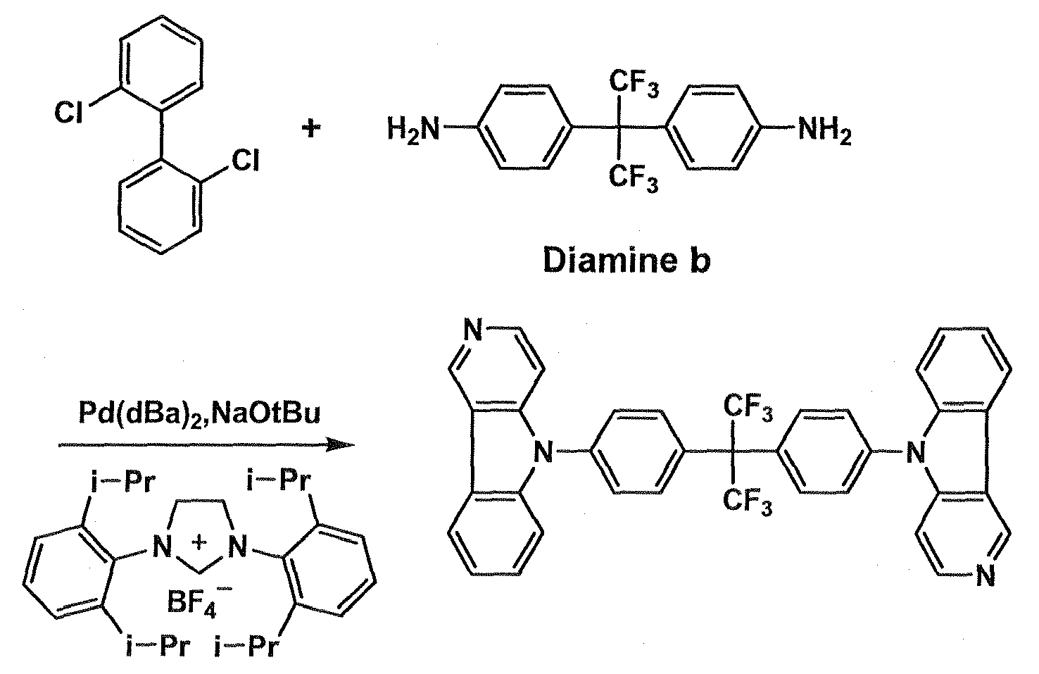
- 0.85 g of 4,4'-dichloro-3,3'-bipyridyl, 0.59 g of diamine b, 44 mg of dibenzylideneacetone palladium, 36mg of imidazolium salt, and 1.09 g of the sodium-tert-butoxide were added to 5 ml of dimethoxy ethane, and stirred for 24 hours at 80 °C. After standing the product to cool, chloroform and water were added to separate an organic layer. The organic layer was washed by water and a saturated sodium chloride solution, and condensed under a reduced pressure. The residue was recrystallized in ethyl acetate, and 0.3 g of colorless crystal of the exemplified compound 143 was obtained.
- The structure of the exemplified compound 143 was identified with a 1H-NMR spectrum and a mass spectroscopy. The spectrum data are as follows:
- MS(FAB) m/z 639 (M+1) 1H-NMR (400MHz, CDCl3) : δ/ppm 7.46 (d, J = 5.7 Hz, 4H), 7.6 - 7.7 (m, 4H), 7.8 - 7.9 (m, 4H), 8.67 (d, J = 5.7 Hz, 4H), 9.51 (S, 4H)
- The exemplified compound 145 was synthesized in the same manner as the exemplified compound 143, except that 3-(2-chlorophenyl)-4-chloropyridine was used, which is a compound prepared by replacing one of the pyridine rings of 4,4'-dichloro-3,3'-bipyridyl with benzene.
- The structure of the exemplified compound 145 was identified with a 1H-NMR spectrum and a mass spectroscopy. The spectrum data of the exemplified compound 145 are as follows:
- MS (FAB) m/z 637 (M+1) 1H-NMR (400MHz, CDCl3) : δ/ppm 7.3 - 7.4 (m, 2H), 7.6 - 7.7 (m, 4H), 7.7 - 7.8 (m, 4H), 7.8 - 7.9 (m, 4H), 8.06 (d, J = 5.3 Hz, 2H), 8.23 (d, J = 7.8 Hz, 2H), 8.56 (d, J = 5.3 Hz, 2H), 8.96 (S, 2H)
- In addition to the above-mentioned synthetic example, an azacarbazole ring of these compounds and its analog may be synthesized according to: J. Chem. Soc., Perkin Trans., 1, 1505-1510 (1999), Pol. J. Chem., 54, 1585 (1980), and Tetrahedron Lett., 41(2000), 481-484. Introduction of a core or a linking group, for example, an aromatic ring, a heterocyclic ring or an alkyl group into synthesized azacarbazole ring or its analog may be carried out by means of a well known method, such as an Ullman coupling, a coupling which used the Pd catalyst, or the Suzuki coupling.
- The compound of the present invention preferably has the molecular weight of not less than 400, more preferably not less than 450, further preferably not less than 600 and specifically preferably not less than 800, whereby the glass transition temperature and the stability of the compound are increased, and a longer life of the organic EL element is obtained.
- The compound of the present invention is used as a constituent of the constituting layers of the organic EL element which will be described later. In the constituting layers of the organic EL element of the present invention, the compound of the present invention is preferably contained in the light emitting layer or in the electron transporting layer (in the electron transporting layer, the compound is used as a hole blocking material), more preferably in the light emitting layer, and specifically preferably as a host compound in the light emitting layer. The compound of the present invention may also be used in other constituting layer of the organic EL element if necessary, to control a variety of properties of the organic EL element.
- The compounds of the present invention are used as materials for the organic EL element (for example, a back light, a flat panel display, a light source of an illumination, a display device, a light source for electrophotography, a recording light source, an exposure light source, a reading light source, a sign, a signboard, an interior, an optical-transmission device). Examples of other usage include extended fields such as: materials for an organic semiconductor laser (for example, a recording light source, an exposure light source, a reading light source, an optical transmission device and a light source for electrophotography); materials for a photorecepter for electrophotography; materials for an organic TFT element (for example, an organic memory device, an organic operation device, an organic switching element); materials for an organic wavelength converter; and materials for a photoelectric conversion device (for example, a solar cell, a photosensor).
- The constituting layers of the organic EL element of the present invention will be explained below in details.
- Preferred examples of the constituting layers of the organic EL element of the present invention will be shown below, however, the present invention is not limited thereto.
- (i): Anode/Light emitting layer/Electron transporting layer/Cathode
- (ii): Anode/Hole transporting layer/Light emitting layer/Electron transporting layer/Cathode
- (iii): Anode/Hole transporting layer/Light emitting layer/Hole blocking layer/Electron transporting layer/Cathode
- (iv): Anode/Hole transporting layer/Light emitting layer/Hole blocking layer/Electron transporting layer/Cathode buffering layer/Cathode
- (v): Anode/Anode buffering layer/Hole transporting layer/Light emitting layer/Hole blocking layer/Electron transporting layer/Cathode buffering layer/Cathode
- For the anode of the organic EL element, a metal, an alloy, or an electroconductive compound each having a high working function (not less than 4 eV), and mixture thereof are preferably used as the electrode material. Specific examples of such an electrode material include a metal such as Au, CuI and a transparent electroconductive material such as indium tin oxide (ITO), SnO2, or ZnO. A material capable of forming an amorphous and transparent conductive layer such as IDIXO (In2O3-ZnO) may also be used. The anode may be prepared by forming a thin layer of the electrode material according to a depositing or spattering method, and by forming the layer into a desired pattern according to a photolithographic method. When required precision of the pattern is not so high (not less than 100 µm), the pattern may be formed by depositing or spattering of the electrode material through a mask having a desired form. When light is emitted through the anode, the transmittance of the anode is preferably 10% or more, and the sheet resistance of the anode is preferably not more than several hundred Ω/□. The thickness of the layer is ordinarily within the range of from 10 nm to 1 µm, and preferably from 10 to 200 nm, although it may vary due to kinds of materials used.
- On the other hand, for the cathode, a metal (also referred to as an electron injecting metal), an alloy, and an electroconductive compound each having a low working function (not more than 4 eV), and a mixture thereof are used as the electrode material. Specific examples of such an electrode material include sodium, sodium-potassium alloy, magnesium, lithium, a magnesium/copper mixture, a magnesium/silver mixture, a magnesium/aluminum mixture, magnesium/indium mixture, an aluminum/aluminum oxide (Al2O3) mixture, indium, a lithium/aluminum mixture, and a rare-earth metal. Among them, a mixture of an electron injecting metal and a metal higher in the working function than that of the electron injecting metal, such as the magnesium/silver mixture, magnesium/aluminum mixture, magnesium/indium mixture, aluminum/aluminum oxide (Al2O3) mixture, lithium/aluminum mixture, or aluminum is suitable from the view point of the electron injecting ability and resistance to oxidation. The cathode can be prepared forming a thin layer of such an electrode material by a method such as a deposition or spattering method. The sheet resistance as the cathode is preferably not more than several hundred Ω/□, and the thickness of the layer is ordinarily from 10 nm to 1 µm, and preferably from 50 to 200 nm. It is preferable in increasing the light emission efficiency that either the anode or the cathode of the organic EL element is transparent or semi-transparent.
- After a layer of the metal described above as a cathode is formed to give a thickness of from 1 to 20 nm, a layer of the transparent electroconductive material as described in the anode is formed on the resulting metal layer, whereby a transparent or semi-transparent cathode can be prepared. Employing the cathode, an element can be manufactured in which both anode and cathode are transparent.
- Next, an injecting layer, a blocking layer, and an electron transporting layer used in the component layer of the organic EL element of the present invention will be explained.
- The injecting layer is optionally provided, for example, an electron injecting layer or a hole injecting layer, and may be provided between the anode and the light emitting layer or hole transporting layer, and between the cathode and the light emitting layer or electron transporting layer as described above.
- The injecting layer herein referred to is a layer provided between the electrode and an organic layer in order to reduce the driving voltage or to improve of light emission efficiency. As the buffer layer there are a hole injecting layer (an anode buffer layer) and an electron injecting layer (a cathode buffer layer), which are described in "Electrode Material" pages 123 - 166, Div. 2 Chapter 2 of "Organic EL element and its frontier of industrialization" (published by NTS Corporation, November 30, 1998) in detail.
- The anode buffer layer (hole injecting layer) is described in, for example, JP-A Nos. 9-45479, 9-260062, and 8-288069, and its examples include a phthalocyanine buffer layer represented by a copper phthalocyanine layer, an oxide buffer layer represented by a vanadium oxide layer, an amorphous carbon buffer layer, a polymer buffer layer employing and an electroconductive polymer such as polyaniline (emeraldine) and polythiophene.
- The cathode buffer layer (electron injecting layer) is described in, for example, JP-A Nos. 6-325871, 9-17574, and 10-74586, in detail, and its examples include a metal buffer layer represented by a strontium or aluminum layer, an alkali metal compound buffer layer represented by a lithium fluoride layer, an alkali earth metal compound buffer layer represented by a magnesium fluoride layer, and an oxide buffer layer represented by an aluminum oxide. The buffer layer (injecting layer) is preferably very thin and has a thickness of preferably from 0.1 to 5 µm depending on kinds of the material used.
- The blocking layer is a layer provided if necessary in addition to the fundamental component layers as described above, and is for example a hole blocking layer as described in JP-A Nos. 11-204258, and 11-204359, and on page 237 of "Organic EL element and its frontier of industrialization" (published by NTS Corporation, November 30, 1998).
- The hole blocking layer is an electron transporting layer in a broad sense, and is a material having an ability of transporting electrons, however, an extremely poor ability of transporting holes, which can increase a recombination probability of electrons and holes by transporting electrons while blocking holes.
- The hole blocking layer of the organic EL element of the present invention is provided adjacent to the light emitting layer. In the present invention, the hole blocking layer preferably contains the above mentioned compounds relating the present invention as a hole blocking material, whereby an organic EL element exhibiting a higher emission efficiency is obtained, further an organic EL element exhibiting a longer life is obtained.
- On the other hand, the electron blocking layer is an hole transporting layer in a broad sense, and is a material having an ability of transporting holes, however, an extremely poor ability of transporting electrons, which can increase a recombination probability of electrons and holes by transporting holes while blocking electrons.
- The light emitting layer of the present invention is a layer where electrons and holes, injected from electrodes, an electron transporting layer or a hole transporting layer, are recombined to emit light. The portions where light emits may be in the light emitting layer or at the interface between the light emitting layer and the layer adjacent thereto.
- The light emitting layer of the present invention preferably contains a host compound and a phosphorescent compound (also referred to as a phosphorescent light emitting compound) which will be described later. In the present invention, the above described compounds relating to the present invention are preferably used as a host compound, whereby an organic EL element exhibiting higher emission efficiency is obtained. Further, other compounds besides the relating compounds to the present invention may also be used as a host compound. In the present invention, a host compound is defined as a compound of which the quantum yield of phosphorescent light emission is less than 0.01.
- A plurality of known host compounds may also be used in combination. Use of a plurality of host compounds makes the control of the transfer of electrons possible, and an organic EL element exhibiting higher light emission efficiency is obtained. Also, use of a plurality of phosphorescent compounds makes it possible to mix different colors of emitted light, and an arbitrary color of emitted light is obtained. Emission of white light is possible by adjusting the types and amounts of doping of mixed phosphorescent compounds, whereby application of the organic EL element to an illuminator or a backlight is possible.
- Among the known host compounds, preferable are the compounds having hole transporting ability, electron transporting ability, effect to prevent a shift of light emission to a longer wavelength side and a high Tg (a glass transition temperature).
- Examples of the known host compounds include the compounds disclosed in the following documents:
- JP-A No. 2001-257076, No. 2002-308855, No. 2001-313179, No. 2002-319491, No. 2001-357977, No. 2002-334786, No. 2002-8860, No. 2002-334787, No. 2002-15871,No. 2002-334788, No. 2002-43056, No. 2002-334789, No. 2002-75645, No. 2002-338579, No. 2002-105445, No. 2002-343568, No. 2002-141173, No. 2002-352957, No. 2002-203683, No. 2002-363227, No. 2002-231453, No. 2003-3165, No. 2002-234888, No. 2003-27048, No. 2002-255934, No. 2002-260861, No. 2002-280183, No. 2002-299060, No. 2002-302516, No. 2002-305083, No. 2002-305084, No. 2002-308837.
- The light emitting layer may contain a host compound having a fluorescence maximum wavelength as a host compound. In this case, by a energy transfer from other host compound or a phosphorescent compound to a fluorescent compound, light emission from a host compound having a fluorescence maximum wavelength is obtained as the result of electroluminescence of an organic EL element. The host compound having a fluorescence maximum wavelength preferably has a high fluorescence quantum yield in the form of solution. Herein, the fluorescence quantum yield is preferably not less than 10%, and more preferably not less than 30%. Examples of the a host compound having a wavelength providing a fluorescence maximum wavelength include a coumarin dye, a cyanine dye, a chloconium dye, a squalenium dye, an oxobenzanthracene dye, a fluorescene dye, a rhodamine dye, a pyrylium dye, a perylene dye, a stilbene dye, and a polythiophene dye. The fluorescence quantum yield can be measured according to a method described in the fourth edition,
Jikken Kagaku Koza 7, Bunko II, p. 362 (1992) published by Maruzen. - A material used in the light emitting layer (hereinafter also referred to as light emitting material) preferably contains a phosphorescent compound together with the host compound described above, whereby an organic EL element exhibiting higher emission efficiency is obtained.
- The phosphorescent compound in the present invention is a compound which emits light from the excited triplet, which can emit phosphorescence at room temperature (25°C), and exhibits a phosphorescent quantum yield at 25 °C of not less than 0.01. The phosphorescent quantum yield at 25 °C is preferably not less than 0.1.
- The phosphorescent quantum yield can be measured according to a method described in the fourth edition "
Jikken Kagaku Koza 7", Bunko II, page 398 (1992) published by Maruzen. The phosphorescent quantum yield can be measured in a solution employing various kinds of solvents. The phosphorescent compound used in the present invention is a compound, in which the phosphorescent quantum yield measured employing any one of the solvents falls within the above-described range. - The light emission of the phosphorescent compound is divided in two types in principle, one is an energy transfer type in which recombination of a carrier occurs on the host to which the carrier is transported to excite the host, the resulting energy is transferred to the phosphorescent compound, and light is emitted from the phosphorescent compound, and the other is a carrier trap type in which recombination of a carrier occurs on the phosphorescent compound which is a carrier trap material, and light is emitted from the phosphorescent compound. However, in each type, energy level of the phosphorescent compound in excited state is lower than that of the host in excited state.
- The phosphorescent compound is suitably selected from those used in the light emitting layer of an organic EL element known in the prior art.
- The phosphorescent compound used in the present invention is preferably a metal complex containing a metal belonging to a group VIII of the periodic, and is more preferably an iridium compound, an osmium compound, a platinum compound (a platinum complex) or a rare earth compound, and most preferably an iridium compound.
- Examples of the phosphorescent compound used in the present invention will be listed below, however, the present invention is not limited thereto. These compounds can be synthesized according to a method described in Inorg. Chem., 40, 1704-1711.


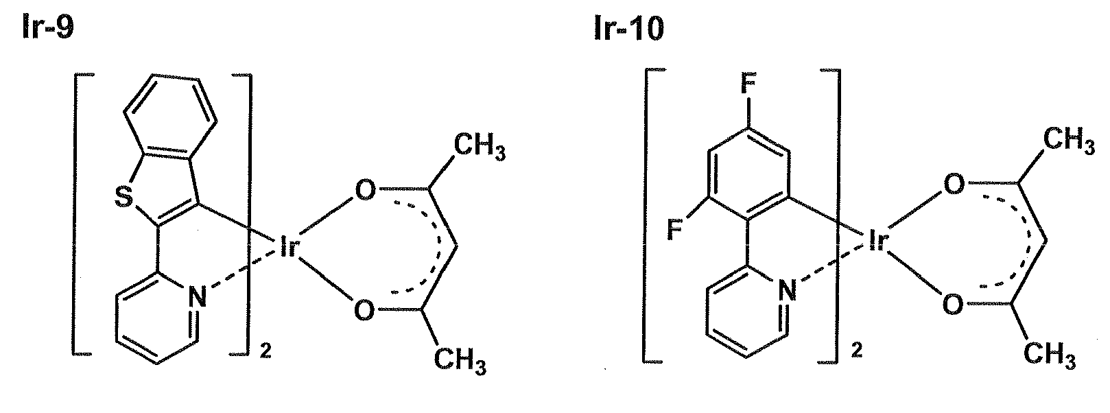


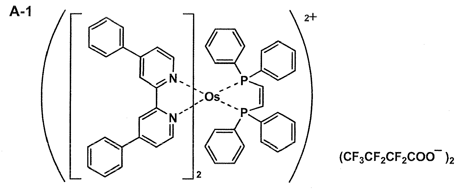


- In the present invention, the wavelength of the phosphorescence maximum of the phosphorescent compound is not specifically limited. Theoretically, the phosphorescence wavelength can be varied by selecting a center metal, a ligand, or a substituent of the ligand. The phosphorescent compound preferably has a wavelength of the phosphorescence maximum in the wavelength region from 380 to 430 nm. Such an organic EL element emitting a blue or white light phosphorescence can provide higher emission efficiency.
- Color of light emitted from the organic EL element or the compound of the present invention is measured by a spectral light meter CS-1000, manufactured by Minolta Co., Ltd., and expressed according to CIE chromaticity diagram described in Fig. 4.16 on page 108 of "Shinpen Shikisai Kagaku Handbook" (Coloring Science Handbook, New Edition), edited by Nihon Shikisai Gakkai, published by Todai Shuppan Kai, 1985.
- The light emitting layer can be formed employing the above-described compounds and a known method such as a vacuum deposition method, a spin coat method, a casting method, an LB method or an ink jet method. The thickness of the light emitting layer is not specifically limited, however, is ordinarily from 5 nm to 5 µm, and preferably from 5 to 200 nm. The light emitting layer may be composed of a single layer comprising one or two or more of the phosphorescent compound or the host compound, or of plural layers comprising the same composition or different composition.
- The hole transporting layer may be either an organic substance or an inorganic substance as long as it has a hole injecting ability, a hole transporting ability or an ability to form a barrier to electrons. Examples of thereof include a triazole derivative, an oxadiazole derivative, an imidazole derivative, a polyarylalkane derivative, a pyrazoline derivative and a pyrazolone derivative, a phenylenediamine derivative, an arylamine derivative, an amino substituted chalcone derivative, an oxazole derivative, a styryl anthracene derivative, a fluorenone derivative, a hydrazone derivative, a stilbene derivative, a silazane derivative, an aniline copolymer, and an electroconductive oligomer, specifically a thiophene oligomer. As the hole transporting material, those described above are used, however, a porphyrin compound, an aromatic tertiary amine compound or a styrylamine compound is preferably used, and, specifically, an aromatic tertiary amine compound is more preferably used.
- Typical examples of the aromatic tertiary amine compound and styrylamine compound include N,N,N',N'-tetraphenyl-4,4'-diaminophenyl, N,N'-diphenyl-N,N'-bis(3-methylphenyl)-[1,1'-biphenyl]-4,4'-diamine (TPD), 2,2-bis(4-di-p-tolylaminophenyl)propane, 1,1-bis(4-di-p-tolylaminophenyl)cyclohexane, N,N,N',N'-tetra-p-tolyl-4,4'-diaminobiphenyl, 1,1-bis(4-di-p-tolylaminophenyl)-4-phenylcyclohexane, bis(4-dimethylamino-2-methylphenyl)phenylmethane, bis(4-di-p-tolylaminophenyl)phenylmethane, N,N'-diphenyl-N,N'-di(4-methoxyphenyl)-4,4'-diaminobiphenyl, N,N,N',N'-tetraphenyl-4,4'-diaminodiphenylether, 4,4'-bis(diphenylamino)quardriphenyl, N,N,N-tri(p-tolyl)amine, 4-(di-p-tolylamino)-4'-[4-(di-p-tolylamino)styryl]stilbene, 4-N,N-diphenylamino-(2-diphenylvinyl)benzene, 3-methoxy-4'-N,N-diphenylaminostylbene, N-phenylcarbazole, compounds described in US Patent No. 5,061,569 which have two condensed aromatic rings in the molecule thereof such as 4,4'-bis[N-(1-naphthyl)-N-phenylamino]biphenyl (NPD), and compounds described in JP-A No. 4-308688 such as 4,4',4"-tris[N-(3-methylphenyl)-N-phenylamino]-triphenylamine (MTDATA) in which three triphenylamine units are bonded in a starburst form.
- A polymer in which the material mentioned above is introduced in the polymer chain or a polymer having the material as the polymer main chain can be also used. As the hole injecting material or the hole transporting material, inorganic compounds such as p-Si and p-SiC are usable.
- The hole transporting layer can be formed by preparing a thin layer of the hole transporting material using a known method such as a vacuum deposition method, a spin coat method, a casting method, an ink jet method, and an LB method. The thickness of the hole transporting layer is not specifically limited, however, is ordinarily from 5 to 5000 nm. The hole transporting layer may be composed of a single layer structure comprising one or two or more of the materials mentioned above.
- The electron transporting layer contains a material having an electron transporting ability, and in a broad sense an electron injecting layer or a hole blocking layer are included in an electron transporting layer. The electron transporting layer can be provided as a single layer or plural layers.
- An electron transporting material (which serves also as a hole blocking material) used in a single electron transporting layer or in the electron transporting layer closest to the cathode when plural electron transporting layers are employed, may be a compound which has a function of transporting electrons injected from a cathode to a light emitting layer. The material used in the electron transporting layer can be optionally selected from known compounds used as electron transporting materials.
- Examples of the material used in the electron transporting layer include a nitro-substituted fluorene derivative, a diphenylquinone derivative, a thiopyran dioxide derivative, a carbodiimide, a fluolenylidenemethane derivative, an anthraquinodimethane, an anthrone derivative, and an oxadiazole derivative. Moreover, a thiadiazole derivative which is formed by substituting the oxygen atom in the oxadiazole ring of the foregoing oxadiazole derivative with a sulfur atom, and a quinoxaline derivative having a quinoxaline ring known as an electron withdrawing group are usable as the electron transporting material.
- A polymer in which the material mentioned above is introduced in the polymer side chain or a polymer having the material as the polymer main chain can be also used.
- A metal complex of an 8-quinolynol derivative such as aluminum tris(8-quinolynol) (Alq), aluminum tris(5,7-dichloro-8-quinolynol), aluminum tris(5,7-dibromo-8-quinolynol), aluminum tris(2-methyl-8-quinolynol), aluminum tris(5-methyl-8-quinolynol), or zinc bis(8-quinolynol) (Znq), and a metal complex formed by replacing the central metal of the foregoing complexes with another metal atom such as In, Mg, Cu, Ca, Sn, Ga or Pb, can be used as the electron transporting material. Furthermore, a metal free or metal-containing phthalocyanine, and a derivative thereof, in which the molecular terminal is replaced by a substituent such as an alkyl group or a sulfonic acid group, are also preferably used as the electron transporting material. The distyrylpyrazine derivative exemplified as a material for the light emitting layer may preferably be employed as the electron transporting material. An inorganic semiconductor such as n-Si and n-SiC may also be used as the electron transporting material in a similar way as in the hole transporting layer.
- The electron transporting layer can be formed employing the above described electron transporting materials and a known method such as a vacuum deposition method, a spin coat method, a casting method, a printing method including an ink jet method or an LB method. The thickness of electron transporting layer is not specifically limited, however, is ordinarily from 5 nm to 5 µm, and preferably from 5 to 200 nm. The electron transporting layer may be composed of a single layer containing one or two or more of the electron transporting material.
- The organic EL element of the present invention is preferably provided on a substrate.
- The substrate (referred to as also base plate, base or support) employed for the organic electroluminescent element of the present invention is not restricted to specific kinds of materials such as glass and plastic, as far as it is transparent. Examples of the substrate preferably used include glass, quartz and light transmissible plastic film. Specifically preferred one is a resin film capable of providing flexibility to the organic EL element.
- Examples of the resin film include films of polyethylene terephthalate (PET), polyethylene naphthalate (PEN), polyethersulfone (PES), polyetherimide, polyetheretherketone, polyphenylene sulfide, polyarylate, polyimide, polycarbonate (PC), cellulose triacetate (TAC), cellulose acetate propionate (CAP). The surface of the resin film may have a layer of an inorganic or organic compound or a hybrid layer of both compounds.
- The external light emission efficiency of the organic electroluminescent element of the present invention is preferably not less than 1%, and more preferably not less than 5% at room temperature. Herein, external quantum yield (%) is represented by the following formula:

- A hue improving filter such as a color filter may be used in combination or a color conversion filter which can convert emission light color from an organic EL element to multi-color employing a fluorescent compound may be used in combination. In the case where the color conversion filter is used, the λmax of the light emitted from the organic EL element is preferably not more than 480 nm.
- For one example, the preparation of the organic EL element, which has the following constitution will be described: Anode/Hole injecting layer/Hole transporting layer/Light emitting layer/Electron transporting layer/Electron injecting layer/Cathode. A thin layer of a desired material for an electrode such as a material of the anode is formed on a suitable substrate by a deposition or sputtering method to prepare the anode, so that the thickness of the layer is not more than 1 µm, and preferably within the range of from 10 to 200 nm. Then the hole injecting layer, the hole transporting layer, the light emitting layer, the electron transporting layer and the electron injecting layer, which constitute the organic EL element, are formed on the resulting anode in that order as organic compound thin layers.
- As methods for formation of the thin layers, as the same as described above, there are a vacuum deposition method and a wet process (for example, a spin coating method, a casting method, an ink jet method, and a printing method), however, a vacuum deposition method, a spin coating method, an ink jet method and a printing method are preferably used, since a uniform layer without a pinhole can be formed. Different methods may be used for formation of different layers. When the vacuum deposition method is used for the thin layer formation method, although conditions of the vacuum deposition differs due to kinds of materials used, vacuum deposition is preferably carried out at a boat temperature of from 50° C to 450° C, at a degree of vacuum of from 10-6 to 10-2 Pa, at a deposition speed of from 0.01 to 50 nm/second, and at a substrate temperature of from -50 to 300° C to form a layer with a thickness of from 0.1 nm to 5 µm, preferably from 5 to 200 nm.
- After these layers has been formed, a thin layer of a material for a cathode is formed thereon to prepare a cathode, employing, for example, a deposition method or sputtering method to give a thickness of not more than 1 µm, and preferably from 50 to 200 nm. Thus, a desired organic EL element is obtained. It is preferred that the layers from the hole injecting layer to the cathode are continuously formed under one time of vacuuming to obtain an organic EL element. However, on the way of the layer formation under vacuum, a different layer formation method by taking the layer out of the vacuum chamber may be inserted. When the different method is used, the process is required to be carried out under a dry inert gas atmosphere.
- In the multicolor display of the present invention, the light emitting layer only is formed using a shadow mask, and the other layers, besides the light emitting layer, are formed employing a vacuum method, a casting method, a spin coat method or a printing method in which patterning employing the shadow mask is not required.
- When the light emitting layer only is formed by patterning, the layer formation, although not specifically limited, is carried out preferably according to a deposition method, an ink jet method or a printing method. When a deposition method is used as the layer formation method, patterning of the layer is preferably carried out employing a shadow mask.
- Further, the organic EL element can be prepared in the reverse order, in which the cathode, the electron injecting layer, the electron transporting layer, the light emitting layer, the hole transporting layer, the hole injecting layer, and the anode are formed in that order. When a direct current voltage, a voltage of 2 to 40 V is applied to thus obtained multicolor display, setting the anode as a + polarity and the cathode as a - polarity, light emission occurs. An alternating current may also be applied to cause light emission. Arbitrary wave shape of alternating current may be used.
- The display of the present invention can be used as a display device, a display, or various light emission sources. The display device or the display, which employs three kinds of organic EL elements emitting a blue light, a red light and a green light can present a full color image.
- Examples of the display device or the display include a television, a personal computer, a mobile device or an AV device, a display for text broadcasting, and an information display used in a car. The display device may be used as specifically a display for reproducing a still image or a moving image. When the display device is used as a display for reproducing a moving image, the driving method may be either a simple matrix (passive matrix) method or an active matrix method.
- Examples of an illuminator include a home lamp, a room lamp in a car, a backlight for a watch or a liquid crystal, a light source for boarding advertisement, a signal device, a light source for a photo memory medium, a light source for an electrophotographic copier, a light source for an optical communication instrument, and a light source for an optical sensor, however, are not limited thereto.
- The organic EL element of the present invention may be an organic EL element having a resonator structure.
- The organic EL element having a resonator structure is applied to a light source for a photo-memory medium, a light source for an electrophotographic copier, a light source for an optical communication instrument, or a light source for a photo-sensor, however, its application is not limited thereto. In the above application, a laser oscillation may be carried out.
- The organic EL element of the present invention can be applied to an organic EL element emitting substantially white light as an illuminator. White light is obtained by mixing plural color lights, which are emitted from plural emission compounds. A combination of the plural color lights may be that of lights of three primary colors, blue, green, and red colors, each having a different emission maximum wavelength, or that of lights of complementary colors such as blue and yellow colors, or blue green and orange colors, each having a different emission maximum wavelength.
- A combination of light emitting materials for obtaining plural color lights may be a combination of materials emitting plural fluorescent or phosphorescent light, or a combination of fluorescent or phosphorescent light emitting-material and colorant which emit light under excitation due to excitation light from the light emitting-materials. In the white light emitting organic EL element of the present invention, a combination of only plural light emitting dopants is used.
- A mask is used only in the process when a light emitting layer, a hole transporting layer or an electron transporting layer is formed, and each organic EL element is simply juxtaposed on the substrate by applying through a mask. Since, other layers are common, patterning with a mask is not necessary, and the layers, for example, the electrode layer, are formed employing a vacuum method, a casting method, a spin coat method, an ink-jet method or a printing method, all over the substrate, whereby productivity is increased. In this method, the light emitting element itself emits white light, which is different from a white light emitting organic EL element composed of an array of light emitting elements of plural colors.
- Light emitting materials used in the light emitting layer are not specifically limited. For example, a back light used in a liquid crystal display is prepared by arbitrary selecting materials from orthometal-complexes (for example, an Ir-complex or a Pt-complex) or from known light emitting compounds and by using the selected materials in combination to emit white light, so that the emitted light fits the wavelength range corresponding to the CF (color filter) property.
- The white light emitting organic EL element of the present invention may be suitably used for a variety of emitting light source, an illuminator for household use or in a vehicle, a kind of a lamp such as a light source for exposure, or for a display device, for example, as a back light of a liquid crystal display.
- Other examples of the usage include: a backlight of a watch, an advertisement signboard, a traffic light, a light source for an optical memory medium, a light source for an electrophotographic copier, a light source for an optical communication processor, a light source for a light sensor and electric appliances for household use having a display device.
- The organic EL element of the present invention can be used as a lamp such as an illuminating lamp or a light source for exposure, as a projection device for projecting an image, or as a display for directly viewing a still image or a moving image. When the element is used in a display for reproducing a moving image, the driving method may be either a simple matrix (passive matrix) method or an active matrix method. The display can present a full color image by employing two or more kinds of organic EL elements each emitting light with a different color. A monochromatic color, for example, a white color can be converted to a full color of BGR, employing a color filter. Further, employing a color conversion filter, light color emitted from the organic EL element can be converted to another color or full color, where the λmax of the light emitted from the organic EL element is preferably not more than 480 nm.
- One example of the display comprising the organic EL element of the present invention will be explained below employing Figures.
- Fig. 1 is a schematic drawing of one example of a display containing an organic EL element. Fig. 1 is a display such as that of a cellular phone, displaying image information due to light emission from the organic EL.
- A display 1 contains a display section A having plural pixels and a control section B carrying out image scanning based on image information to display an image in the display section A. The control section B is electrically connected to the display section A, transmits a scanning signal and an image data signal to each of the plural pixels based on image information from the exterior, and conducts image scanning which emits light from each pixel due to the scanning signal according to the image data signal, whereby an image is displayed on the display section A.
- Fig. 2 is a schematic drawing of a display section A. The display section A contains a substrate,
plural pixels 3, and a wiring section containingplural scanning lines 5 and plural data lines 6. The main members of the display section A will be explained below. In Fig. 2, light frompixels 3 is emitted in the direction of an arrow. - The
plural scanning lines 5 andplural data lines 6 of the wiring section 2 each are composed of an electroconductive material, thelines 5 and thelines 6 being crossed with each other at a right angle, and connected with thepixels 3 at the crossed points (not illustrated). - The
plural pixels 3, when the scanning signal is applied from thescanning lines 5, receive the data signal from thedata lines 6, and emit light corresponding to the image data received. Provision of red light emitting pixels, green light emitting pixels, and blue light emitting pixels side by side on the same substrate can display a full color image. - Next, an emission process of pixels will be explained.
- Fig. 3 is a schematic drawing of a pixel. The pixel contains an
organic EL element 10, a switchingtransistor 11, a drivingtransistor 12, and acapacitor 13. When a pixel with a red light emitting organic EL element, a pixel with a green light emitting organic EL element, and a pixel with a blue light emitting organic EL element are provided side by side on the same substrate, a full color image can be displayed. - In Fig. 3, an image data signal is applied through the
data lines 6 from the control section B to a drain of the switchingtransistor 11, and when a scanning signal is applied to a gate of the switchingtransistor 11 through thescanning lines 5 from the control section B, the switchingtransistor 11 is switched on, and the image signal data applied to the drain is transmitted to thecapacitor 13 and the gate of the drivingtransistor 12. - The
capacitor 13 is charged according to the electric potential of the image data signal transmitted, and the drivingtransistor 12 is switched on. In the drivingtransistor 12, the drain is connected to anelectric source line 7, and the source to anorganic EL element 10. Current is supplied from theelectric source line 7 to theorganic EL element 10 according to the electric potential of the image data signal applied to the gate. - The scanning signal is transmitted to the
next scanning line 5 according to the successive scanning of the control section B, the switchingtransistor 11 is switched off. Even if the switchingtransistor 11 is switched off, the drivingtransistor 12 is turned on since thecapacitor 13 maintains a charged potential of image data signal, and light emission from theorganic EL element 10 continues until the next scanning signal is applied. When the next scanning signal is applied according the successive scanning, the drivingtransistor 12 works according to an electric potential of the next image data signal synchronized with the scanning signal, and light is emitted from theorganic EL element 10. - That is, light is emitted from the
organic EL element 10 in each of theplural pixels 3 due to the switchingtransistor 11 as an active element and the drivingtransistor 12 each being provided in theorganic EL element 10 of each of theplural pixels 3. This emission process is called an active matrix process. - Herein, light emission from the
organic EL element 10 may be emission with plural gradations according to image signal data of multiple value having plural gradation potentials, or emission due to on-off according to a binary value of the image data signals. - The electric potential of the
capacitor 13 may maintain till the next application of the scanning signal, or may be discharged immediately before the next scanning signal is applied. - In the present invention, light emission may be carried out employing a passive matrix method as well as the active matrix method as described above. The passive matrix method is one in which light is emitted from the organic EL element according to the data signal only when the scanning signals are scanned.
- Fig. 4 is a schematic drawing of a display employing a passive matrix method.
- In Fig. 4,
pixels 3 are provided between thescanning lines 5 and thedata lines 6, crossing with each other. When scanning signal is applied toscanning line 5 according to successive scanning,pixel 3 connecting thescanning line 5 emits according to the image data signal. The passive matrix method has no active element in thepixel 3, which reduces manufacturing cost of a display. - A pattern was formed on a substrate (100 mm x 100 mm x 1.1 mm) composed of a glass plate and a 100 nm ITO (indium tin oxide) layer (NA45 manufactured by NH Technoglass Co., Ltd.) as an anode. Then the resulting transparent substrate having the ITO transparent electrode was subjected to ultrasonic washing in i-propyl alcohol and dried by a dry nitrogen gas and subjected to UV-ozone cleaning for 5 minutes. Thus obtained transparent substrate was fixed on a substrate holder of a vacuum deposition apparatus available on the market. Further, 200 mg of α-NPD was placed in a first resistive heating molybdenum boat, 200 mg of exemplified compound 9 was put in a second resistive heating molybdenum boat, 200 mg of bathocuproine (BCP) was placed in a third resistive heating molybdenum boat, 100 mg of Ir-12 was placed in a fourth resistive heating molybdenum boat, and 200 mg of Alq3 was placed in a fifth resistive heating molybdenum boat.
- The resulting boats were set in the vacuum deposition apparatus, and pressure in the vacuum tank was reduced to 4 x 10⁻⁴ Pa. Then, the boat carrying α-NPD being heated by supplying an electric current to the boat, α-NPD was deposited onto the transparent substrate at a depositing speed of 0.1 nm/sec to form a first hole transporting layer. After that, the boat carrying Exemplified compound 9 as a host compound and the boat carrying Ir-12 being heated by supplying an electric current to both boats, Exemplified compound 9 at a depositing speed of 0.2 nm/sec and Ir-12 at a depositing speed of 0.012 nm/sec were co-deposited onto the resulting hole transporting layer to form a light emitting layer. The temperature of the substrate at the time of the deposition was room temperature. Subsequently, the boat carrying BCP being heated by supplying an electric current to the boat, BCP was deposited onto the resulting light emitting layer at a depositing speed of 0.1 nm/sec to form a hole blocking layer with a thickness of 10 nm. Further, the boat carrying Alq3 being heated by supplying an electric current to the boat, Alq3 was deposited onto the resulting hole blocking layer at a depositing speed of 0.1 nm/sec to form an electron transporting layer with a thickness of 40 nm. The temperature of the substrate at the time of the deposition was room temperature.
- After that, a 0.5 nm thick lithium fluoride layer and a 110 nm thick aluminum layer were deposited on the resulting material to form a cathode. Thus, Organic EL Element No. 1-1 was prepared. Organic EL Element Nos. 1-2 to 1-21 were prepared in the same manner as Organic EL Element No. 1-1 above, except that Exemplified compound 9 used as a host compound was replaced by the compounds shown in Table 1. The structures of the compounds used above are shown below:


- The Organic EL Element Nos. 1-1 to 1-21 obtained above were evaluated as follows.
- Luminance (cd/m2) was measured by using a spectral radiance meter CS-1000 produced by Konica Minolta Sensing Inc.
- Electric current of 2.5 mA/cm2 was supplied to each sample at 23°C in an atmosphere of a dry nitrogen gas, and the external quantum efficiency (%) of each sample was measured. The external quantum efficiency (%) was calculated from the date obtained by being measured through a spectral radiance meter CS-1000 produced by Konica Minolta Sensing Inc.
- In the following table, the measured luminance and external quantum efficiency were expressed by relative values when each of the luminance and the external quantum efficiency values of Organic EL Element No. 1-15 was set as 100.
- The results are shown in the following table.
Organic EL Element No. Host Compound Luminance External Quantum Efficiency Remarks 1-1 9 220 221 Inv. 1-2 10 180 179 Inv. 1-3 13 215 217 Inv. 1-4 16 160 165 Inv. 1-5 28 205 202 Inv. 1-6 33 155 153 Inv. 1-7 39 215 215 Inv. 1-8 50 213 212 Inv. 1-9 53 189 190 Inv. 1-10 56 212 210 Inv. 1-11 64 217 217 Inv. 1-12 71 201 200 Inv. 1-13 79 170 172 Inv. 1-14 90 180 179 Inv. 1-15 CBP 100 100 Comp. 1-16 105 199 201 Inv. 1-17 122 213 213 Inv. 1-18 123 196 198 Inv. 1-19 131 192 191 Inv. 1-20 132 190 191 Inv. 1-21 140 198 198 Inv. Inv.: Present Invention, Comp. : Comparative Sample - As is clear from the above table, the organic EL elements of the present invention exhibited higher luminance values and considerably higher external quantum efficiency values compared to those of the comparative organic EL element.
- A pattern was formed on a substrate (100 mm x 100 mm x 1.1 mm) composed of a glass plate and a 100 nm ITO (indium tin oxide) layer (manufactured by NH Technoglass Co., Ltd.) as an anode. Then the resulting transparent substrate having the ITO transparent electrode was subjected to ultrasonic washing in i-propyl alcohol and dried by a dry nitrogen gas and subjected to UV-ozone cleaning for 5 minutes. Thus obtained transparent substrate was fixed on a substrate holder of a vacuum deposition apparatus available on the market. Further, 200 mg of α-NPD was placed in a first resistive heating molybdenum boat, 200 mg of CBP was placed in a second resistive heating molybdenum boat, 200 mg of Exemplified compound 9 as a hole blocking material was placed in a third resistive heating molybdenum boat, 100 mg of Ir-1 was placed in a fourth resistive heating molybdenum boat, and 200 mg of Alq3 was placed in a fifth resistive heating molybdenum boat.
- The resulting boats were set in the vacuum deposition apparatus, and pressure in the vacuum tank was reduced to 4 x 10⁻⁴ Pa. Then, the boat carrying α-NPD being heated by supplying an electric current to the boat, α-NPD was deposited onto the transparent substrate at a depositing speed of 0.1 nm/sec to form a first hole transporting layer. After that, the boat carrying CBP and the boat carrying Ir-1 being heated by supplying an electric current to both boats, CBP at a depositing speed of 0.2 nm/sec and Ir-1 at a depositing speed of 0.012 nm/sec were co-deposited onto the resulting hole transporting layer to form a light emitting layer. The temperature of the substrate at the time of the deposition was room temperature. Subsequently, the boat carrying Exemplified compound 9 being heated by supplying an electric current to the boat, Exemplified compound 9 was deposited onto the resulting light emitting layer at a depositing speed of 0.1 nm/sec to form a hole blocking layer with a thickness of 10 nm. Further, the boat carrying Alq3 being heated by supplying an electric current to the boat, Alq3 was deposited onto the resulting hole blocking layer at a depositing speed of 0.1 nm/sec to form an electron transporting layer with a thickness of 40 nm. The temperature of the substrate at the time of the deposition was room temperature.
- After that, a 0.5 nm thick lithium fluoride layer and a 110 nm thick aluminum layer were deposited on the resulting layer to form a cathode. Thus, Organic EL Element No. 2-1 was prepared. Organic EL Element Nos. 2-2 to 1-20 were prepared in the same manner as Organic EL Element No. 2-1, except that Exemplified compound 9 used as a hole blocking compound was replaced by the compounds shown in the following table.
- The luminance and external quantum efficiency of Organic EL Element Nos. 2-1 to 2-20 were evaluated in the same manner as Example 1. Further, the life of the organic EL element was evaluated in a method described below.
- A period in which an initial emission intensity of an organic EL element decreased to half of it was defined as a half-life period (τ 0.5) and used as an index of the life of an organic EL element, the emission intensity being measured by supplying a constant electric current of 2.5 mA/cm2 at 23° C in an atmosphere of a dry nitrogen gas. A spectral radiance meter CS-1000 produced by Konica Minolta Sensing Inc. was used for the measurement of the life of an organic EL element.
- The results are shown in the following table. In the following table, the measured luminance, external quantum efficiency and life shown in the following table were expressed by relative values when each of the luminance, external quantum efficiency and life values of Organic EL Element No. 2-12 was set as 100.
Organic EL Element No. Hole Blocking Material Luminance External Quantum Efficiency Life Remarks 2-1 9 120 120 325 Inv. 2-2 11 130 129 534 Inv. 2-3 15 125 123 330 Inv. 2-4 16 120 122 357 Inv. 2-5 23 105 103 296 Inv. 2-6 40 122 120 440 Inv. 2-7 50 125 126 600 Inv. 2-8 53 110 112 320 Inv. 2-9 56 124 122 764 Inv. 2-10 79 106 105 250 Inv. 2-11 88 103 102 305 Inv. 2-12 BCP 100 100 100 Comp. 2-13 73 118 118 621 Inv. 2-14 74 114 115 832 Inv. 2-15 105 120 120 537 Inv. 2-16 119 115 114 945 Inv. 2-17 123 112 111 584 Inv. 2-18 131 110 110 482 Inv. 2-19 132 113 112 561 Inv. 2-20 140 121 123 556 Inv. Inv.: Present Invention, Comp. : Comparative Sample - As is clear from the above table, the organic EL elements of the present invention exhibited higher luminance values, higher external quantum efficiency values and longer lives compared to those of the comparative organic EL element.
- Organic EL Element Nos. 3-1 to 3-8 were prepared in the same manner as Organic EL Element No. 1-1 described in Example 1, except that the host compound in the light emitting layer was replaced by the compounds shown in the following table, Ir-12 was replaced by Ir-1 and BCP was replaced by B-Alq.

- The luminance and external quantum efficiency of Organic EL Element Nos. 3-1 to 3-8 were evaluated in the same manner as Example 1. Further, the life of the organic EL element was evaluated in a method described below.
- Each organic EL element was reserved at 85 °C for 24 hours, and the luminance of each organic EL element before and after the reservation was measured by passing through a constant current of 2.5 mA/cm2. The ratio of luminance before and after the reservation was calculated according to the following equation and used as a criterion of storage stability.

- The results are given in the following table. Each value of luminance, external quantum efficiency and storage stability given in the following table was expressed as a relative value when each value for Organic EL Element Nos. 3-6 was set as 100.
Organic EL Element No. Host Compound Storage Stability (%) Remarks 3-1 180 90 Inv. 3-2 175 85 Inv. 3-3 82 88 Inv. 3-4 184 82 Inv. 3-5 183 86 Inv. 3-6 CBP 48 Comp. 3-7 186 53 Inv. 3-8 187 64 Inv. Inv.: Present Invention, Comp. : Comparative Sample - As is clear in the above table, the organic EL elements of the present invention exhibited higher luminance values, higher external quantum efficiency values and higher storage stability compared to those of the comparative organic EL element. Among these, compounds relating to Formula (1-12) having molecular weight of 450 or more gave specifically good results.
- Organic EL Element Nos.4-1 to 4-8 were prepared in the same manner as Organic EL Element No. 1-1 described in Example 1, except that the host compound in the light emitting layer was replaced by the compounds shown in the following table, Ir-12 was replaced by Ir-1 and BCP was replaced by B-Alq.
- The luminance and external quantum efficiency of Organic EL Element Nos. 4-1 to 4-8 were evaluated in the same manner as Example 1. Further, the 50 °C driving life of the organic EL element was evaluated in a method described below. (50 °C driving life)
- Each organic EL element was driven under a constant current giving a initial luminance of 1000 cd/m2 and a period in which the luminance decreased to 1/2 (500 cd/m2) of the initial value was determined. This period was used as a criterion of the 50 °C driving life. Each value of the 50 °C driving life was expressed by a relative value when the value of 50 °C driving life of the comparative sample of Organic EL Element No. 4-6 was set as 100.
- The results are given in the following table. Each value of luminance, external quantum given in the following table was expressed as a relative value when each value for Organic EL Element 4-6 was set as 100.
Organic EL Element No. Host Compound 50 °C Driving Life Remarks 4-1 185 730 Inv. 4-2 74 685 Inv. 4-3 139 725 Inv. 4-4 144 755 Inv. 4-5 89 780 Inv. 4-6 CBP 100 Comp. 4-7 186 132 Inv. 4-8 187 253 Inv. Inv.: Present Invention, Comp. : Comparative Sample - As is clear in the above table, the organic EL elements of the present invention exhibited higher luminance, higher external quantum efficiency and longer 50 °C driving lives compared to those of the comparative organic EL element. Among these, compounds relating to Formula (1-13) having molecular weight of 450 or more gave specifically good results.
- Organic EL Element Nos. 5-1 to 5-8 were prepared in the same manner as Organic EL Element No. 1-1 described in Example 1, except that the host compound in the light emitting layer was replaced by the compounds shown in the following table, Ir-12 was replaced by Ir-1 and BCP was replaced by B-Alq.
- The luminance and external quantum efficiency of Organic EL Element Nos. 5-1 to 5-8 were evaluated in the same manner as Example 1. Further, initial life-time of the organic EL element was evaluated in a method described below.
- Each organic EL element was driven under a constant current giving a initial luminance of 1000 cd/m2 and a period in which the luminance decreased to 90% (900 cd/m2) of the initial value was determined. This period was used as a criterion of the initial lifetime. Each value of the initial lifetime was expressed by a relative value when the value initial degradation of the comparative sample of Organic EL Element No. 5-6 was set as 100.
- The results are given in the following table. Each value of measured luminance, external quantum given in the following table was expressed as a relative value when each value for Organic EL Element 5-6 was set as 100.
Organic EL Element No. Host Compound Initial Lifetime Remarks 5-1 118 555 Inv. 5-2 123 485 Inv. 5-3 73 550 Inv. 5-4 48 490 Inv. 5-5 130 535 Inv. 5-6 CBP 100 Comp. 5-7 188 126 Inv. 5-8 187 198 Inv. Inv. : Present Invention, Comp. : Comparative Sample - As is clear in the above table, the organic EL elements of the present invention exhibited higher luminance, higher external quantum efficiency and longer initial life-time compared to those of the comparative organic EL element. Among these, compounds relating to Formula (1-11) gave specifically good results.
- Organic EL Element Nos. 6-1 to 6-8 were prepared in the same manner as Organic EL Element No. 1-1 described in Example 1, except that the host compound in the light emitting layer was replaced by the compounds shown in the following table, Ir-12 was replaced by Ir-1 and BCP was replaced by B-Alq.
- The luminance and external quantum efficiency of Organic EL Element Nos. 6-1 to 6-8 were evaluated in the same manner as Example 1. Further, driving voltage of the organic EL element was evaluated in a method described below.
- Driving voltage represents the voltage of an organic EL element when it is driven under a current of 2.5 mA/cm2. A difference between the driving voltages of the organic EL element and the comparative Organic EL Element No. 6-6 was determined.
- Driving Voltage (V) = Voltage of Organic EL Element No. 6-6 under driving (V) - Voltage of the organic EL element of the present invention under driving (V)
- The results are given in the following table. Each value of measured luminance, external quantum given in the following table was expressed as a relative value when each value for Organic EL Element 6-6 was set as 100.
Organic EL Element No. Host Compound Driving Voltage Remarks 6-1 14 1.3 Inv. 6-2 16 1.4 Inv. 6-3 52 1.5 Inv. 6-4 89 1.2 Inv. 6-5 48 1.2 Inv. 6-6 CBP 0 Comp. 6-7 186 0.8 Inv. 6-8 187 0.8 Inv. Inv.: Present Invention, Comp. : Comparative Sample - As is clear in the above table, the organic EL elements of the present invention exhibited higher luminance, higher external quantum efficiency and superior driving voltage compared to those of the comparative organic EL element. Among these, compounds relating to Formulae (1-1) to (1-4) gave specifically good results.
- Organic EL Element Nos. 7-1 to 7-8 were prepared in the same manner as Organic EL Element No. 2-12 described in Example 2, except that the host compound in the light emitting layer (CBP) was replaced by the Exemplified compound 130 and BCP in the hole blocking layer was replaced by the hole blocking materials shown in the following table.
- The luminance, external quantum efficiency and storage stability of Organic EL Element Nos. 7-1 to 7-8 were evaluated in the same manner as Example 3.
- The results are given in the following table. Each value of measured luminance, external quantum efficiency given in the following table was expressed as a relative value when each value for Organic EL Element 7-6 was set as 100.
Organic EL Element No. Hole Blocking Material Storage Stability Remarks 7-1 180 92 Inv. 7-2 175 88 Inv. 7-3 82 89 Inv. 7-4 184 86 Inv. 7-5 183 90 Inv. 7-6 B-Alq 67 Comp. 7-7 186 67 Inv. 7-8 187 76 Inv. Inv.: Present Invention, Comp. : Comparative Sample - As is clear in the above table, the organic EL elements of the present invention exhibited higher luminance, higher external quantum efficiency and superior storage stability compared to those of the comparative organic EL element. Among these, compounds relating to Formula (1-12) having molecular weight of 450 or more gave specifically good results.
- Organic EL Element Nos. 8-1 to 8-8 were prepared in the same manner as Organic EL Element No. 2-12 described in Example 2, except that the host compound in the light emitting layer (CBP) was replaced by the Exemplified compound 130 and BCP in the hole blocking layer was replaced by the hole blocking materials shown in the following table. «Evaluation of Organic EL Element Nos. 8-1 to 8-8»
- The luminance, external quantum efficiency and 50 °C driving life of Organic EL Element Nos. 8-1 to 8-8 were evaluated in the same manner as Example 4.
- The results are given in the following table. Each value of measured luminance, external quantum efficiency and 50 °C driving life given in the following table was expressed as a relative value when each value for Organic EL Element 8-6 was set as 100.
Organic EL Element No. Hole Blocking Material 50°C Driving Life Remarks 8-1 185 420 Inv. 8-2 74 385 Inv. 8-3 139 390 Inv. 8-4 144 365 Inv. 8-5 89 440 Inv. 8-6 B-Alq 100 Comp. 8-7 186 121 Inv. 8-8 187 173 Inv. Inv. : Present Invention, Comp. : Comparative Sample - As is clear in the above table, the organic EL elements of the present invention exhibited higher luminance, higher external quantum efficiency and longer 50 °C driving lives compared to those of the comparative organic EL element. Among these, compounds relating to Formula (1-13) having molecular weight of 450 or more gave specifically good results.
- Organic EL Element Nos. 9-1 to 9-8 were prepared in the same manner as Organic EL Element No. 2-12 described in Example 2, except that the host compound in the light emitting layer (CBP) was replaced by the Exemplified compound 130 and BCP in the hole blocking layer was replaced by the hole blocking materials shown in the following table.
- The luminance, external quantum efficiency and initial life of Organic EL Element Nos. 9-1 to 9-8 were evaluated in the same manner as Example 5.
- The results are given in the following table. Each value of measured luminance, external quantum efficiency and initial life given in the following table was expressed as a relative value when each value for Organic EL Element 9-6 was set as 100.
Organic EL Element No. Hole Blocking Material Initial Lifetime Remarks 9-1 118 321 Inv. 9-2 123 298 Inv. 9-3 73 350 Inv. 9-4 48 310 Inv. 9-5 130 350 Inv. 9-6 B-Alq 100 Comp. 9-7 188 112 Inv. 9-8 187 141 Inv. Inv.: Present Invention, Comp.: Comparative Sample - As is clear in the above table, the organic EL elements of the present invention exhibited higher luminance, higher external quantum efficiency and longer initial lives compared to those of the comparative organic EL element. Among these, compounds relating to Formula (1-11) gave specifically good results.
- Organic EL Element Nos. 10-1 to 10-8 were prepared in the same manner as Organic EL Element No. 2-12 described in Example 2, except that the host compound in the light emitting layer (CBP) was replaced by the Exemplified compound 130 and BCP in the hole blocking layer was replaced by the hole blocking materials shown in the following table. «Evaluation of Organic EL Element Nos. 10-1 to 10-8»
- The luminance, external quantum efficiency and driving voltage of Organic EL Element Nos. 10-1 to 10-8 were evaluated in the same manner as Example 6.
- The results are given in the following table. Each value of measured luminance and external quantum efficiency given in the following table was expressed as a relative value when each value for Organic EL Element 10-6 was set as 100. Each driving voltage was obtained as a voltage difference between the voltage of each organic EL element and that of Organic EL Element No. 10-6.
Organic EL Element No. Host Compound Driving Voltage Remarks 10-1 14 0.9 Inv. 10-2 16 1.0 Inv. 10-3 52 1.0 Inv. 10-4 89 0.8 Inv. 10-5 48 0.9 Inv. 10-6 B-Alq 0 Comp. 10-7 186 0.4 Inv. 10-8 187 0.4 Inv. Inv. : Present Invention, Comp. : Comparative Sample - As is clear in the above table, the organic EL elements of the present invention exhibited higher luminance, higher external quantum efficiency and superior driving voltages compared to those of the comparative organic EL element. Among these, compounds relating to Formulae (1-1) to (1-4) gave specifically good results.
- Organic EL Element No. 1-1 of the present invention prepared in Example 1, Organic EL Element No. 2-7 of the present invention prepared in Example 2 and an organic EL element prepared in the same manner as Organic EL Element No. 2-7 of the present invention, except that the phosphorescent compound was replaced by Exemplified compound Ir-9, were juxtaposed on the same substrate to prepare a full color display device driven by an active matrix method, illustrated in Fig. 1. In Fig. 2, a schematic drawing of only display section A is shown. Namely, on the same substitute, a wiring section containing
plural scanning lines 5 andplural data lines 6 and juxtaposed plural pixels 3 (pixels emitting red light, pixels emitting green light and pixels emitting blue light) are provided. Theplural scanning lines 5 andplural data lines 6 of the wiring section 2 are composed of an electroconductive material. Thelines 5 and thelines 6 are crossing with each other at a right angle to form a lattice, and connected to thepixels 3 at the crossed points (not illustrated). Theplural pixels 3 are driven by an active matrix method in which each pixel contained an organic EL element emitting a corresponding color light and active elements including a switching transistor and a driving transistor. When scanning signals are applied through thescanning lines 5, image data signals are received throughdata lines 6, and emission occurs according to the received image data. By juxtaposing red light emitting pixels, green light emitting pixels, and blue light emitting pixels side by side on the same substrate, display of a full color image becomes possible. - By driving the full color display device, a sharp full color moving picture with high external quantum efficiency and high durability was obtained.
- The present invention can provide an organic electroluminescent element and a display device exhibiting high emission efficiency and a long life.
Claims (63)
- An organic electroluminescent element comprising a pair of electrodes having therebetween at least one constituting layer containing a phosphorescent light emitting layer, wherein one of the constituting layer contains a compound represented by Formula (1):

wherein Z1 represents an aromatic heterocylic ring which may have a substituent; Z2 represents an aromatic heterocylic ring which may have a substituent or an aromatic hydrocarbon ring which may have a substituent; Z3 represents a divalent linking group or a single bond; and R101 represents a hydrogen atom or a substituent. - The organic electroluminescent element of claim 1, wherein Z1 of the compound represented by Formula (1) is a 6-membered ring.
- The organic electroluminescent element of claim 1 or claim 2, wherein Z2 of the compound represented by Formula (1) is a 6-membered ring.
- The organic electroluminescent element of any one of claims 1 to 3, wherein Z3 of the compound represented by Formula (1) is a single bond.
- The organic electroluminescent element of any one of claims 1 to 4, wherein the compound represented by Formula (1) has a molecular weight of 450 or more.
- The organic electroluminescent element of any one of claims 1 to 5, wherein the compound represented by Formula (1) is further represented by Formula (1-1).

wherein R501 - R507 each independently represents a hydrogen atom or a substituent. - The organic electroluminescent element of any one of claims 1 to 5, wherein the compound represented by Formula (1) is further represented by Formula (1-2).

wherein R511 R517 each independently represents a hydrogen atom or a substituent. - The organic electroluminescent element of any one of claims 1 to 5, wherein the compound represented by Formula (1) is further represented by Formula (1-3).

wherein R521 - R527 each independently represents a hydrogen atom or a substituent. - The organic electroluminescent element of any one of claims 1 to 5, wherein the compound represented by Formula (1) is further represented by Formula (1-4).

wherein R531 - R537 each independently represents a hydrogen atom or a substituent. - The organic electroluminescent element of any one of claims 1 to 5, wherein the compound represented by Formula (1) is further represented by Formula (1-5).

wherein R541 - R548 each independently represents a hydrogen atom or a substituent. - The organic electroluminescent element of any one of claims 1 to 5, wherein the compound represented by Formula (1) is further represented by Formula (1-6).

wherein R551 - R558 each independently represents a hydrogen atom or a substituent. - The organic electroluminescent element of any one of claims 1 to 5, wherein the compound represented by Formula (1) is further represented by Formula (1-7).

wherein R561 - R567 each independently represents a hydrogen atom or a substituent. - The organic electroluminescent element of any one of claims 1 to 5, wherein the compound represented by Formula (1) is further represented by Formula (1-8).
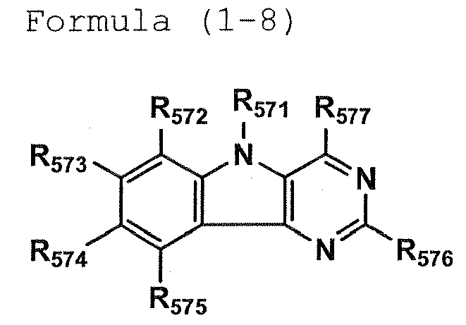
wherein R571 - R577 each independently represents a hydrogen atom or a substituent. - The organic electroluminescent element of any one of claims 1 to 5, wherein the compound represented by Formula (1) is further represented by Formula (1-9).
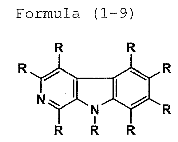
wherein each R represents a hydrogen atom or a substituent and a plurality of R may be the same or may be different from each other. - The organic electroluminescent element of any one of claims 1 to 5, wherein the compound represented by Formula (1) is further represented by Formula (1-10).

wherein each R represents a hydrogen atom or a substituent and a plurality of R may be the same or may be different from each other. - The organic electroluminescent element of any one of claims 1 to 5, wherein the compound represented by Formula (1) has at least one of groups represented by Formulae (2-1) to (2-8).

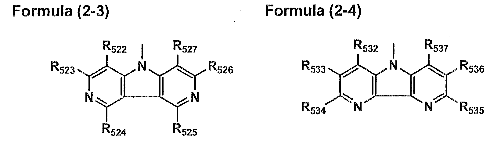

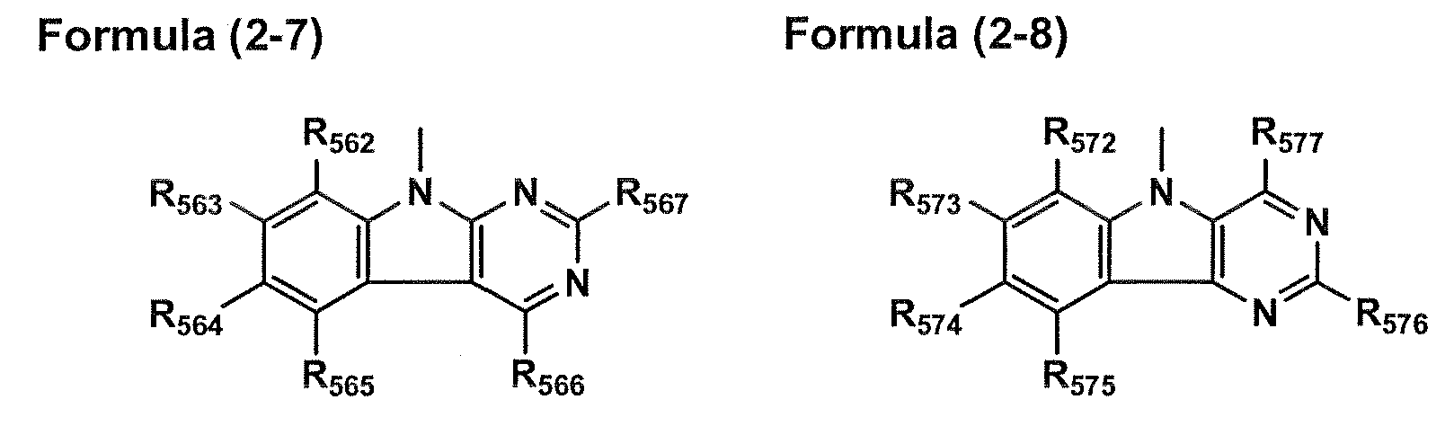
wherein(a) in Formula (2-1), R502 - R507 each independently represents a hydrogen atom or a substituent;(b) in Formula (2-2), R512 - R517 each independently represents a hydrogen atom or a substituent;(c) in Formula (2-3) , R522 - R527 each independently represents a hydrogen atom or a substituent;(d) in Formula (2-4), R532 - R537 each independently represents a hydrogen atom or a substituent;(e) in Formula (2-5), R542 - R548 each independently represents a hydrogen atom or a substituent;(f) in Formula (2-6), R552 - R558 each independently represents a hydrogen atom or a substituent;(g) in Formula (2-7), R562 - R567 each independently represents a hydrogen atom or a substituent; and(h) in Formula (2-8), R572 - R577 each independently represents a hydrogen atom or a substituent. - The organic electroluminescent element of any one of claims 1 to 5, wherein the compound represented by Formula (1) is further represented by Formula (3).
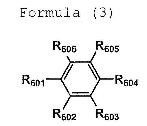
wherein R601 - R606 each independently represents a hydrogen atom or a substituent and at least one of R601 - R606 is represented by one of Formulae (2-1) to (2-4). - The organic electroluminescent element of any one of claims 1 to 5, wherein the compound represented by Formula (1) is further represented by Formula (4).

wherein R611 - R620 each independently represents a hydrogen atom or a substituent and at least one of R611 - R620 is represented by one of Formulae (2-1) to (2-4). - The organic electroluminescent element of any one of claims 1 to 5, wherein the compound represented by Formula (1) is further represented by Formula (5).

wherein R621 - R623 each independently represents a hydrogen atom or a substituent and at least one of R621 - R623 is represented by one of Formulae (2-1) to (2-4). - The organic electroluminescent element of any one of claims 1 to 5, wherein the compound represented by Formula (1) is further represented by Formula (6).

wherein R631 - R645 each independently represents a hydrogen atom or a substituent and at least one of R631 R645 is represented by one of Formulae (2-1) to (2-4). - The organic electroluminescent element of any one of claims 1 to 5, wherein the compound represented by Formula (1) is further represented by Formula (7).
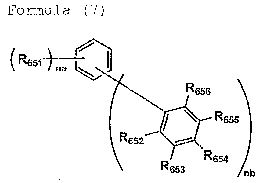
wherein R651 - R656 each independently represents a hydrogen atom or a substituent and at least one of R651 - R656 is represented by one of Formulae (2-1) to (2-4); na represents an integer of 0 to 5; and nb represents an integer of 1 to 6, provided that a sum of na and nb is 6. - The organic electroluminescent element of any one of claims 1 to 5, wherein the compound represented by Formula (1) is further represented by Formula (8).

wherein R661 - R672 each independently represents a hydrogen atom or a substituent and at least one of R661 - R672 is represented by one of Formulae (2-1) to (2-4). - The organic electroluminescent element of any one of claims 1 to 5, wherein the compound represented by Formula (1) is further represented by Formula (9).

wherein R681 - R688 each independently represents a hydrogen atom or a substituent and at least one of R681 - R688 is represented by one of Formulae (2-1) to (2-4). - The organic electroluminescent element of any one of claims 1 to 5, wherein the compound represented by Formula (1) is further represented by Formula (10).

wherein R691 - R700 each independently represents a hydrogen atom or a substituent and at least one of R691 - R700 is represented by one of Formulae (2-1) to (2-4); and L1 represents a divalent linking group. - The organic electroluminescent element of any one of claims 1 to 5, wherein the compound represented by Formula (1) is further represented by Formula (11).
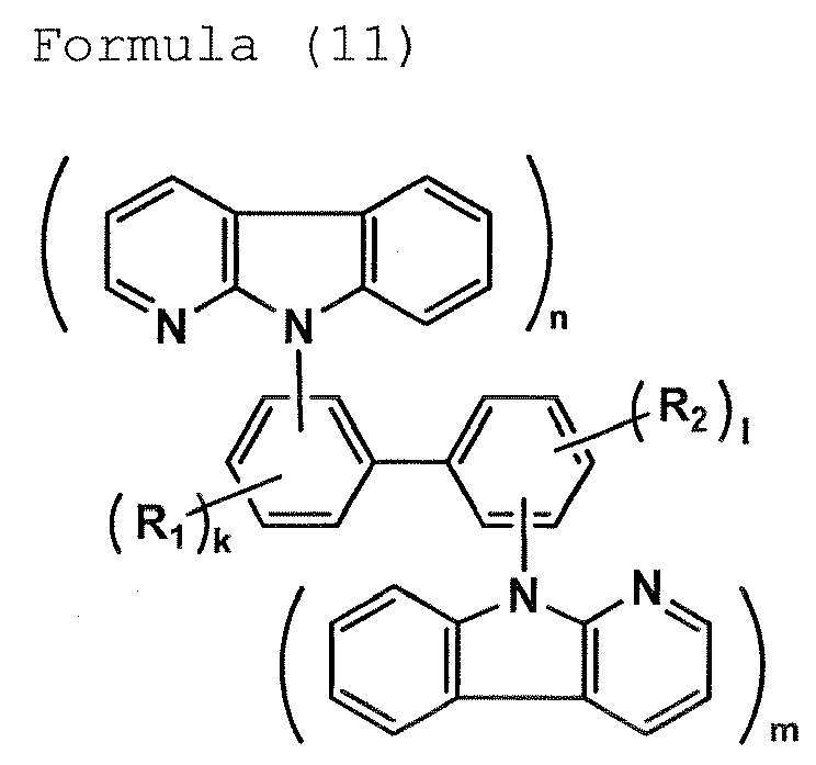
wherein R1 and R2 each independently represents a hydrogen atom or a substituent; n and m each represents an integer of 1 to 2; and k and 1 each represents an integer of 3 to 4, provided that n + k = 5 and l + m = 5. - The organic electroluminescent element of any one of claims 1 to 5, wherein the compound represented by Formula (1) is further represented by Formula (12).

wherein R1 and R2 each independently represents a hydrogen atom or a substituent; n and m each represents an integer of 1 to 2; and k and 1 each represents an integer of 3 to 4, provided that n + k = 5 and l + m = 5. - The organic electroluminescent element of any one of claims 1 to 5, wherein the compound represented by Formula (1) is further represented by Formula (13).

wherein R1 and R2 each independently represents a hydrogen atom or a substituent; n and m each represents an integer of 1 to 2; and k and l each represents an integer of 3 to 4, provided that n + k = 5 and l + m = 5. - The organic electroluminescent element of any one of claims 1 to 5, wherein the compound represented by Formula (1) is further represented by Formula (14).

wherein R1 and R2 each independently represents a hydrogen atom or a substituent; n and m each represents an integer of 1 to 2; and k and l each represents an integer of 3 to 4, provided that n + k = 5 and l + m = 5. - The organic electroluminescent element of any one of claims 1 to 5, wherein the compound represented by Formula (1) is further represented by Formula (15).

wherein R1 and R2 each independently represents a hydrogen atom or a substituent; n and m each represents an integer of 1 to 2; k and l each represents an integer of 3 to 4, provided that n + k = 5 and l + m = 5; and Z1, Z2, Z3 and Z4 each represent a 6-membered aromatic heterocyclic ring containing a nitrogen atom. - The organic electroluminescent element of any one of claims 1 to 5, wherein the compound represented by Formula (1) is further represented by Formula (16).

wherein o and p each represents an integer of 1 to 3; Ar1 and Ar2 each represents an arylene group or a divalent aromatic heterocyclic group; Z1 and Z2 each represents a 6-membered aromatic heterocyclic ring containing a nitrogen atom; and L represents a divalent linking group. - The organic electroluminescent element of any one of claims 1 to 5, wherein the compound represented by Formula (1) is further represented by Formula (17).

wherein o and p each represents an integer of 1 to 3; Ar1 and Ar2 each represents an arylene group or a divalent aromatic heterocyclic group; Z1, Z2, Z3 and Z4 each represents a 6-membered aromatic heterocyclic ring containing a nitrogen atom; and L represents a divalent linking group. - The organic electroluminescent element of any one of claims 1 to 31, wherein the light emitting layer contains the compound represented by Formula (1).
- The organic electroluminescent element of any one of claims 1 to 32, wherein at least one of the constituting layers is a hole blocking layer and the hole blocking layer contains the compound represented by Formula (1).
- The organic electroluminescent element of any one of claims 1 to 33 which emits blue light.
- The organic electroluminescent element of any one of claims 1 to 33 which emits white light.
- A display device having the organic electroluminescent element of any one of claims 1 to 35.
- An organic electroluminescent element comprising a pair of electrodes having therebetween at least one constituting layer containing a phosphorescent light emitting layer, wherein one of the constituting layer contains a compound represented by Formula (1-11):

wherein Z1 represents an aromatic heterocylic ring which may have a substituent; Z2 represents an aromatic heterocylic ring which may have a substituent or an aromatic hydrocarbon ring which may have a substituent; Z3 represents a divalent linking group or a single bond; L represents a divalent linking group; and the two groups linked by L may be the same or different from each other. - The organic electroluminescent element of claim 37, wherein Z1 of the compound represented by Formula (1-11) is a 6-membered ring.
- The organic electroluminescent element of claim 37 or claim 38, wherein Z2 of the compound represented by Formula (1-11) is a 6-membered ring.
- The organic electroluminescent element of any one of claims 37 to 39, wherein Z3 of the compound represented by Formula (1-11) is a single bond.
- The organic electroluminescent element of any one of claims 37 to 40, wherein the compound represented by Formula (1-11) has a molecular weight of 450 or more.
- The organic electroluminescent element of any one of claims 37 to 41, wherein the light emitting layer contains the compound represented by Formula (1-11).
- The organic electroluminescent element of any one of claims 37 to 42, wherein at least one of the constituting layers is a hole blocking layer and the hole blocking layer contains the compound represented by Formula (1-11).
- The organic electroluminescent element of any one of claims 37 to 43 which emits blue light.
- The organic electroluminescent element of any one of claims 37 to 43 which emits white light.
- A display device having the organic electroluminescent element of any one of claims 37 to 45.
- An organic electroluminescent element comprising a pair of electrodes having therebetween at least one constituting layer containing a phosphorescent light emitting layer, wherein one of the constituting layer contains a compound represented by Formula (1-12):
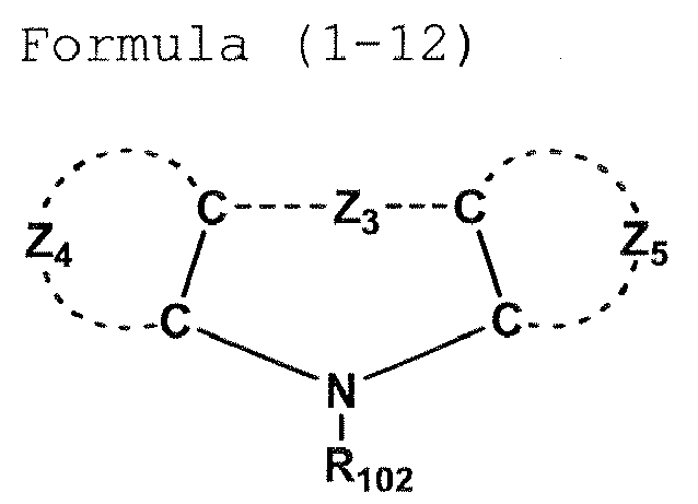
wherein R102 represents an alkyl group which may have a substituent, a cycloalkyl group which may have a substituent, an aryl group which may have a substituent or a heterocyclic group which may have a substituent; Z4 and Z5 each independently represents an atom group which is necessary to form a 5 - 7 membered heterocylic ring containing nitrogen; and Z3 represents a divalent linking group or a single bond. - The organic electroluminescent element of claim 47, wherein Z3 of the compound represented by Formula (1-12) is a single bond.
- The organic electroluminescent element of claim 47 or claim 48, wherein the compound represented by Formula (1-12) has a molecular weight of 450 or more.
- The organic electroluminescent element of any one of claims 47 to 49, wherein the light emitting layer contains the compound represented by Formula (1-12).
- The organic electroluminescent element of any one of claims 47 to 50, wherein at least one of the constituting layers is a hole blocking layer and the hole blocking layer contains the compound represented by Formula (1-12).
- The organic electroluminescent element of any one of claims 47 to 51 which emits blue light.
- The organic electroluminescent element of any one of claims 47 to 51 which emits white light.
- A display device having the organic electroluminescent element of any one of claims 47 to 53.
- An organic electroluminescent element comprising a pair of electrodes having therebetween at least one constituting layer containing a phosphorescent light emitting layer, wherein one of the constituting layer contains a compound represented by Formula (1-13):

wherein R103 represents an alkyl group which may have a substituent, a cycloalkyl group which may have a substituent, an aryl group which may have a substituent or a heterocyclic group which may have a substituent; R104 represents a hydrogen atom or a substituent; and Z6 and Z7 each independently represents an atom group which is necessary to form a 5 - 7 membered heterocylic ring containing nitrogen. - The organic electroluminescent element of claim 55, wherein Z6 of the compound represented by Formula (1-13) is a 6-membered ring.
- The organic electroluminescent element of claim 55 or claim 56, wherein Z7 of the compound represented by Formula (1-13) is a 6-membered ring.
- The organic electroluminescent element of any one of claims 55 to 57, wherein the compound represented by Formula (1-13) has a molecular weight of 450 or more.
- The organic electroluminescent element of any one of claims 55 to 58, wherein the light emitting layer contains the compound represented by Formula (1-13).
- The organic electroluminescent element of any one of claims 55 to 59, wherein at least one of the constituting layers is a hole blocking layer and the hole blocking layer contains the compound represented by Formula (1-13).
- The organic electroluminescent element of any one of claims 55 to 60 which emits blue light.
- The organic electroluminescent element of any one of claims 55 to 60 which emits white light.
- A display device having the organic electroluminescent element of any one of claims 55 to 62.
Priority Applications (1)
| Application Number | Priority Date | Filing Date | Title |
|---|---|---|---|
| EP10167857.1A EP2236579B1 (en) | 2003-04-23 | 2004-04-20 | Organic electroluminescent element and display |
Applications Claiming Priority (3)
| Application Number | Priority Date | Filing Date | Title |
|---|---|---|---|
| JP2003117886 | 2003-04-23 | ||
| JP2004015487 | 2004-01-23 | ||
| PCT/JP2004/005603 WO2004095889A1 (en) | 2003-04-23 | 2004-04-20 | Organic electroluminescent device and display |
Related Child Applications (2)
| Application Number | Title | Priority Date | Filing Date |
|---|---|---|---|
| EP10167857.1A Division EP2236579B1 (en) | 2003-04-23 | 2004-04-20 | Organic electroluminescent element and display |
| EP10167857.1A Division-Into EP2236579B1 (en) | 2003-04-23 | 2004-04-20 | Organic electroluminescent element and display |
Publications (3)
| Publication Number | Publication Date |
|---|---|
| EP1617711A1 true EP1617711A1 (en) | 2006-01-18 |
| EP1617711A4 EP1617711A4 (en) | 2009-08-19 |
| EP1617711B1 EP1617711B1 (en) | 2016-08-17 |
Family
ID=33312627
Family Applications (3)
| Application Number | Title | Priority Date | Filing Date |
|---|---|---|---|
| EP04728453.4A Expired - Lifetime EP1617711B1 (en) | 2003-04-23 | 2004-04-20 | Organic electroluminescent device and display |
| EP20040728448 Expired - Lifetime EP1617710B1 (en) | 2003-04-23 | 2004-04-20 | Material for organic electroluminescent device, organic electroluminescent device, illuminating device and display |
| EP10167857.1A Expired - Lifetime EP2236579B1 (en) | 2003-04-23 | 2004-04-20 | Organic electroluminescent element and display |
Family Applications After (2)
| Application Number | Title | Priority Date | Filing Date |
|---|---|---|---|
| EP20040728448 Expired - Lifetime EP1617710B1 (en) | 2003-04-23 | 2004-04-20 | Material for organic electroluminescent device, organic electroluminescent device, illuminating device and display |
| EP10167857.1A Expired - Lifetime EP2236579B1 (en) | 2003-04-23 | 2004-04-20 | Organic electroluminescent element and display |
Country Status (4)
| Country | Link |
|---|---|
| US (3) | US7326475B2 (en) |
| EP (3) | EP1617711B1 (en) |
| JP (3) | JP4635870B2 (en) |
| WO (3) | WO2004095889A1 (en) |
Cited By (419)
| Publication number | Priority date | Publication date | Assignee | Title |
|---|---|---|---|---|
| DE102008015526A1 (en) | 2008-03-25 | 2009-10-01 | Merck Patent Gmbh | metal complexes |
| DE102008027005A1 (en) | 2008-06-05 | 2009-12-10 | Merck Patent Gmbh | Organic electronic device containing metal complexes |
| DE102008036247A1 (en) | 2008-08-04 | 2010-02-11 | Merck Patent Gmbh | Electronic devices containing metal complexes |
| DE102008036982A1 (en) | 2008-08-08 | 2010-02-11 | Merck Patent Gmbh | Organic electroluminescent device |
| DE102008057051A1 (en) | 2008-11-13 | 2010-05-20 | Merck Patent Gmbh | Materials for organic electroluminescent devices |
| DE102008057050A1 (en) | 2008-11-13 | 2010-05-20 | Merck Patent Gmbh | Materials for organic electroluminescent devices |
| DE102008063490A1 (en) | 2008-12-17 | 2010-06-24 | Merck Patent Gmbh | Organic electroluminescent device |
| DE102008063470A1 (en) | 2008-12-17 | 2010-07-01 | Merck Patent Gmbh | Organic electroluminescent device |
| WO2010086089A1 (en) | 2009-02-02 | 2010-08-05 | Merck Patent Gmbh | Metal complexes |
| DE102009009277A1 (en) | 2009-02-17 | 2010-08-19 | Merck Patent Gmbh | Organic electronic device |
| WO2010099852A1 (en) | 2009-03-02 | 2010-09-10 | Merck Patent Gmbh | Metal complexes having azaborol ligands and electronic device having the same |
| DE102009013041A1 (en) | 2009-03-13 | 2010-09-16 | Merck Patent Gmbh | Materials for organic electroluminescent devices |
| DE102009012346A1 (en) | 2009-03-09 | 2010-09-16 | Merck Patent Gmbh | Organic electroluminescent device |
| WO2010115498A1 (en) | 2009-04-09 | 2010-10-14 | Merck Patent Gmbh | Organic electroluminescence device |
| DE102009023155A1 (en) | 2009-05-29 | 2010-12-02 | Merck Patent Gmbh | Materials for organic electroluminescent devices |
| WO2010149259A2 (en) | 2009-06-22 | 2010-12-29 | Merck Patent Gmbh | Conducting formulation |
| DE102009031021A1 (en) | 2009-06-30 | 2011-01-05 | Merck Patent Gmbh | Materials for organic electroluminescent devices |
| WO2011006574A1 (en) | 2009-07-14 | 2011-01-20 | Merck Patent Gmbh | Materials for organic electroluminescent devices |
| WO2011015265A2 (en) | 2009-08-04 | 2011-02-10 | Merck Patent Gmbh | Electronic devices comprising multi cyclic hydrocarbons |
| DE102009041414A1 (en) | 2009-09-16 | 2011-03-17 | Merck Patent Gmbh | metal complexes |
| DE102009041289A1 (en) | 2009-09-16 | 2011-03-17 | Merck Patent Gmbh | Organic electroluminescent device |
| WO2011032686A1 (en) | 2009-09-16 | 2011-03-24 | Merck Patent Gmbh | Formulas for producing electronic devices |
| DE102009042693A1 (en) | 2009-09-23 | 2011-03-24 | Merck Patent Gmbh | Materials for electronic devices |
| WO2011042107A2 (en) | 2009-10-08 | 2011-04-14 | Merck Patent Gmbh | Materials for organic electroluminescent devices |
| DE102009049587A1 (en) | 2009-10-16 | 2011-04-21 | Merck Patent Gmbh | metal complexes |
| DE102009053645A1 (en) | 2009-11-17 | 2011-05-19 | Merck Patent Gmbh | Materials for organic electroluminescent device |
| WO2011057706A2 (en) | 2009-11-14 | 2011-05-19 | Merck Patent Gmbh | Materials for electronic devices |
| DE102009053644A1 (en) | 2009-11-17 | 2011-05-19 | Merck Patent Gmbh | Materials for organic electroluminescent devices |
| DE102009053836A1 (en) | 2009-11-18 | 2011-05-26 | Merck Patent Gmbh | Materials for organic electroluminescent devices |
| WO2011066898A1 (en) | 2009-12-05 | 2011-06-09 | Merck Patent Gmbh | Electronic device containing metal complexes |
| DE102009023154A1 (en) | 2009-05-29 | 2011-06-16 | Merck Patent Gmbh | A composition comprising at least one emitter compound and at least one polymer having conjugation-interrupting units |
| WO2011076326A1 (en) | 2009-12-22 | 2011-06-30 | Merck Patent Gmbh | Electroluminescent functional surfactants |
| WO2011076324A1 (en) | 2009-12-23 | 2011-06-30 | Merck Patent Gmbh | Compositions comprising organic semiconducting compounds |
| WO2011076325A1 (en) | 2009-12-23 | 2011-06-30 | Merck Patent Gmbh | Compositions comprising polymeric binders |
| WO2011076314A1 (en) | 2009-12-22 | 2011-06-30 | Merck Patent Gmbh | Electroluminescent formulations |
| WO2011076323A1 (en) | 2009-12-22 | 2011-06-30 | Merck Patent Gmbh | Formulations comprising phase-separated functional materials |
| DE102010004803A1 (en) | 2010-01-16 | 2011-07-21 | Merck Patent GmbH, 64293 | Materials for organic electroluminescent devices |
| WO2011088877A1 (en) | 2010-01-25 | 2011-07-28 | Merck Patent Gmbh | Compounds for electronic devices |
| WO2011091838A1 (en) | 2010-01-29 | 2011-08-04 | Merck Patent Gmbh | Styrene-based copolymers, in particular for use in optoelectronic components |
| DE102010009193A1 (en) | 2010-02-24 | 2011-08-25 | Merck Patent GmbH, 64293 | Fluorine-fluorine associates |
| DE102010010481A1 (en) | 2010-03-06 | 2011-09-08 | Merck Patent Gmbh | Organic electroluminescent device |
| DE102010009903A1 (en) | 2010-03-02 | 2011-09-08 | Merck Patent Gmbh | Connections for electronic devices |
| WO2011110275A2 (en) | 2010-03-11 | 2011-09-15 | Merck Patent Gmbh | Radiative fibers |
| WO2011110277A1 (en) | 2010-03-11 | 2011-09-15 | Merck Patent Gmbh | Fibers in therapy and cosmetics |
| WO2011116865A1 (en) | 2010-03-25 | 2011-09-29 | Merck Patent Gmbh | Materials for organic electroluminescence devices |
| WO2011116869A1 (en) | 2010-03-26 | 2011-09-29 | Merck Patent Gmbh | Compounds for electronic devices |
| WO2011116857A1 (en) | 2010-03-23 | 2011-09-29 | Merck Patent Gmbh | Materials for organic electroluminescent devices |
| WO2011128035A1 (en) | 2010-04-12 | 2011-10-20 | Merck Patent Gmbh | Composition and method for preparation of organic electronic devices |
| WO2011128034A1 (en) | 2010-04-12 | 2011-10-20 | Merck Patent Gmbh | Composition having improved performance |
| DE102010014933A1 (en) | 2010-04-14 | 2011-10-20 | Merck Patent Gmbh | Materials for electronic devices |
| DE102010018321A1 (en) | 2010-04-27 | 2011-10-27 | Merck Patent Gmbh | Organic electroluminescent device |
| DE102010019306A1 (en) | 2010-05-04 | 2011-11-10 | Merck Patent Gmbh | Organic electroluminescent devices |
| WO2011137922A1 (en) | 2010-05-03 | 2011-11-10 | Merck Patent Gmbh | Formulations and electronic devices |
| WO2011141120A1 (en) | 2010-05-14 | 2011-11-17 | Merck Patent Gmbh | Metal complexes |
| DE102010020044A1 (en) | 2010-05-11 | 2011-11-17 | Merck Patent Gmbh | Organic electroluminescent device |
| WO2011147522A1 (en) | 2010-05-27 | 2011-12-01 | Merck Patent Gmbh | Compositions comprising quantum dots |
| WO2011147523A1 (en) | 2010-05-27 | 2011-12-01 | Merck Patent Gmbh | Formulation and method for preparation of organic electronic devices |
| DE102009022858A1 (en) | 2009-05-27 | 2011-12-15 | Merck Patent Gmbh | Organic electroluminescent devices |
| WO2011157339A1 (en) | 2010-06-15 | 2011-12-22 | Merck Patent Gmbh | Metal complexes |
| WO2011157346A1 (en) | 2010-06-18 | 2011-12-22 | Merck Patent Gmbh | Compounds for electronic devices |
| DE102010024542A1 (en) | 2010-06-22 | 2011-12-22 | Merck Patent Gmbh | Materials for electronic devices |
| WO2011160758A1 (en) | 2010-06-24 | 2011-12-29 | Merck Patent Gmbh | Materials for organic electroluminescent devices |
| DE102010027317A1 (en) | 2010-07-16 | 2012-01-19 | Merck Patent Gmbh | metal complexes |
| DE102010027218A1 (en) | 2010-07-15 | 2012-01-19 | Merck Patent Gmbh | Organic complexes containing metals |
| DE102010027316A1 (en) | 2010-07-16 | 2012-01-19 | Merck Patent Gmbh | metal complexes |
| DE102010027320A1 (en) | 2010-07-16 | 2012-01-19 | Merck Patent Gmbh | Polymeric materials for organic electroluminescent devices |
| DE102010027319A1 (en) | 2010-07-16 | 2012-01-19 | Merck Patent Gmbh | metal complexes |
| WO2012013270A1 (en) | 2010-07-26 | 2012-02-02 | Merck Patent Gmbh | Nanocrystals in devices |
| WO2012013272A1 (en) | 2010-07-26 | 2012-02-02 | Merck Patent Gmbh | Quantum dots and hosts |
| WO2012013271A1 (en) | 2010-07-30 | 2012-02-02 | Merck Patent Gmbh | Organic electroluminescent device |
| WO2012016630A1 (en) | 2010-08-05 | 2012-02-09 | Merck Patent Gmbh | Materials for electronic devices |
| DE102010045405A1 (en) | 2010-09-15 | 2012-03-15 | Merck Patent Gmbh | Materials for organic electroluminescent devices |
| WO2012038029A1 (en) | 2010-09-24 | 2012-03-29 | Merck Patent Gmbh | Phosphorus-containing metal complexes |
| DE102010046412A1 (en) | 2010-09-23 | 2012-03-29 | Merck Patent Gmbh | Metal ligand coordination compounds |
| WO2012045384A1 (en) | 2010-10-09 | 2012-04-12 | Merck Patent Gmbh | Materials for electronic devices |
| WO2012048900A1 (en) | 2010-10-14 | 2012-04-19 | Fraunhofer-Gesellschaft Zur Förderung Der Angewandten Forschung E.V. . | Materials for organic electroluminescence devices |
| WO2012048780A1 (en) | 2010-10-15 | 2012-04-19 | Merck Patent Gmbh | Compounds for electronic devices |
| DE102010048608A1 (en) | 2010-10-15 | 2012-04-19 | Merck Patent Gmbh | Materials for organic electroluminescent devices |
| DE102010054525A1 (en) | 2010-12-15 | 2012-04-26 | Merck Patent Gmbh | Organic electroluminescent device |
| WO2012069121A1 (en) | 2010-11-24 | 2012-05-31 | Merck Patent Gmbh | Materials for organic electroluminescent devices |
| DE102010054316A1 (en) | 2010-12-13 | 2012-06-14 | Merck Patent Gmbh | Substituted tetraarylbenzenes |
| WO2012079741A1 (en) | 2010-12-15 | 2012-06-21 | Merck Patent Gmbh | Metal complexes |
| DE102010055901A1 (en) | 2010-12-23 | 2012-06-28 | Merck Patent Gmbh | Organic electroluminescent device |
| WO2012084115A1 (en) | 2010-12-23 | 2012-06-28 | Merck Patent Gmbh | Organic electroluminescent device |
| WO2012095143A1 (en) | 2011-01-13 | 2012-07-19 | Merck Patent Gmbh | Compounds for organic electroluminescent devices |
| DE102012000064A1 (en) | 2011-01-21 | 2012-07-26 | Merck Patent Gmbh | New heterocyclic compound excluding 9,10-dioxa-4b-aza-9a-phospha-indeno(1,2-a)indene and 9,10-dioxa-4b-aza-indeno(1,2-a)indene, useful e.g. as matrix material for fluorescent or phosphorescent emitters of electronic devices |
| EP2482159A2 (en) | 2011-01-28 | 2012-08-01 | Honeywell International, Inc. | Methods and reconfigurable systems to optimize the performance of a condition based health maintenance system |
| WO2012107163A1 (en) | 2011-02-12 | 2012-08-16 | Merck Patent Gmbh | Substituted dibenzonaphthacene |
| WO2012107158A1 (en) | 2011-02-10 | 2012-08-16 | Merck Patent Gmbh | 1,3-dioxan-5-one compounds |
| WO2012110182A1 (en) | 2011-02-17 | 2012-08-23 | Merck Patent Gmbh | Compounds for electronic devices |
| WO2012110178A1 (en) | 2011-02-14 | 2012-08-23 | Merck Patent Gmbh | Device and method for treatment of cells and cell tissue |
| WO2012126566A1 (en) | 2011-03-24 | 2012-09-27 | Merck Patent Gmbh | Organic ionic functional materials |
| WO2012136296A1 (en) | 2011-04-04 | 2012-10-11 | Merck Patent Gmbh | Metal complexes |
| WO2012136295A1 (en) | 2011-04-05 | 2012-10-11 | Merck Patent Gmbh | Organic electroluminescent device |
| WO2012139692A1 (en) | 2011-04-13 | 2012-10-18 | Merck Patent Gmbh | Materials for electronic devices |
| WO2012139693A1 (en) | 2011-04-13 | 2012-10-18 | Merck Patent Gmbh | Compounds for electronic devices |
| WO2012143080A2 (en) | 2011-04-18 | 2012-10-26 | Merck Patent Gmbh | Materials for organic electroluminescent devices |
| WO2012143079A1 (en) | 2011-04-18 | 2012-10-26 | Merck Patent Gmbh | Compounds for electronic devices |
| WO2012149992A1 (en) | 2011-05-04 | 2012-11-08 | Merck Patent Gmbh | Device for preserving fresh goods |
| WO2012150001A1 (en) | 2011-05-05 | 2012-11-08 | Merck Patent Gmbh | Compounds for electronic devices |
| WO2012149999A1 (en) | 2011-05-05 | 2012-11-08 | Merck Patent Gmbh | Compounds for electronic devices |
| WO2012152366A1 (en) | 2011-05-12 | 2012-11-15 | Merck Patent Gmbh | Organic ionic compounds, compositions and electronic devices |
| DE102012007810A1 (en) | 2011-05-16 | 2012-11-22 | Merck Patent Gmbh | Electronic device, preferably organic electroluminescent device comprises a transition metal compound exhibiting a transition metal-tin bond |
| DE102011102586A1 (en) | 2011-05-27 | 2012-11-29 | Merck Patent Gmbh | Organic electronic device |
| WO2012163471A1 (en) | 2011-06-03 | 2012-12-06 | Merck Patent Gmbh | Metal complexes |
| WO2012163465A1 (en) | 2011-06-03 | 2012-12-06 | Merck Patent Gmbh | Organic electroluminescence device |
| WO2013000531A1 (en) | 2011-06-28 | 2013-01-03 | Merck Patent Gmbh | Metal complexes |
| WO2013017192A1 (en) | 2011-08-03 | 2013-02-07 | Merck Patent Gmbh | Materials for electronic devices |
| WO2013017189A1 (en) | 2011-07-29 | 2013-02-07 | Merck Patent Gmbh | Compounds for electronic devices |
| WO2013020631A1 (en) | 2011-08-10 | 2013-02-14 | Merck Patent Gmbh | Metal complexes |
| US8377332B2 (en) | 2008-06-10 | 2013-02-19 | Basf Se | Transition metal complexes and use thereof in organic light emitting diodes—III |
| DE102012016192A1 (en) | 2011-08-19 | 2013-02-21 | Merck Patent Gmbh | New compounds capable of forming hydrogen bonds are useful in electronic device, e.g. organic electroluminescent device, organic light-emitting transistor and organic light-emitting electrochemical cell |
| WO2013026515A1 (en) | 2011-08-22 | 2013-02-28 | Merck Patent Gmbh | Organic electroluminescence device |
| WO2013041176A1 (en) | 2011-09-21 | 2013-03-28 | Merck Patent Gmbh | Carbazole derivatives for organic electroluminescence devices |
| US8410270B2 (en) | 2008-06-10 | 2013-04-02 | Basf Se | Transition metal complexes and use thereof in organic light-emitting diodes V |
| DE102011116165A1 (en) | 2011-10-14 | 2013-04-18 | Merck Patent Gmbh | Benzodioxepin-3-one compounds |
| WO2013056776A1 (en) | 2011-10-20 | 2013-04-25 | Merck Patent Gmbh | Materials for organic electroluminescent devices |
| WO2013060418A1 (en) | 2011-10-27 | 2013-05-02 | Merck Patent Gmbh | Materials for electronic devices |
| WO2013060411A1 (en) | 2011-10-28 | 2013-05-02 | Merck Patent Gmbh | Hyperbranched polymers, methods for producing same, and use of same in electronic devices |
| WO2013064206A1 (en) | 2011-11-01 | 2013-05-10 | Merck Patent Gmbh | Organic electroluminescent device |
| WO2013083216A1 (en) | 2011-11-17 | 2013-06-13 | Merck Patent Gmbh | Spiro dihydroacridine derivatives and the use thereof as materials for organic electroluminescence devices |
| WO2013087142A1 (en) | 2011-12-12 | 2013-06-20 | Merck Patent Gmbh | Compounds for electronic devices |
| DE102012022880A1 (en) | 2011-12-22 | 2013-06-27 | Merck Patent Gmbh | Electronic device e.g. organic integrated circuits, organic field-effect transistors, organic thin-film transistors, organic light emitting transistors, comprises an organic layer comprising substituted heteroaryl compounds |
| WO2013097920A1 (en) | 2011-12-27 | 2013-07-04 | Merck Patent Gmbh | Metal complexes comprising 1,2,3-triazoles |
| WO2013107487A1 (en) | 2012-01-16 | 2013-07-25 | Merck Patent Gmbh | Organic metal complexes |
| WO2013113349A1 (en) | 2012-01-30 | 2013-08-08 | Merck Patent Gmbh | Nanocrystals on fibers |
| WO2013120577A1 (en) | 2012-02-14 | 2013-08-22 | Merck Patent Gmbh | Spirobifluorene compounds for organic electroluminescent devices |
| WO2013135352A1 (en) | 2012-03-15 | 2013-09-19 | Merck Patent Gmbh | Electronic devices |
| WO2013139431A1 (en) | 2012-03-23 | 2013-09-26 | Merck Patent Gmbh | 9,9'-spirobixanthene derivatives for electroluminescent devices |
| WO2013174471A1 (en) | 2012-05-24 | 2013-11-28 | Merck Patent Gmbh | Metal complexes comprising condensed heteroaromatic rings |
| WO2013182263A1 (en) | 2012-06-06 | 2013-12-12 | Merck Patent Gmbh | Phenanthrene compounds for organic electronic devices |
| US8610110B2 (en) | 2008-03-11 | 2013-12-17 | Merck Patent Gmbh | Optoelectronic component comprising neutral transition metal complexes |
| US8618317B2 (en) | 2008-07-17 | 2013-12-31 | Merck Patent Gmbh | Organic electroluminescence device |
| WO2014008982A1 (en) | 2012-07-13 | 2014-01-16 | Merck Patent Gmbh | Metal complexes |
| WO2014008967A2 (en) | 2012-07-10 | 2014-01-16 | Merck Patent Gmbh | Materials for organic electroluminescent devices |
| US8637168B2 (en) | 2008-10-08 | 2014-01-28 | Merck Patent Gmbh | Materials for organic electroluminescence devices |
| WO2014015935A2 (en) | 2012-07-23 | 2014-01-30 | Merck Patent Gmbh | Compounds and organic electronic devices |
| WO2014015938A1 (en) | 2012-07-23 | 2014-01-30 | Merck Patent Gmbh | Derivatives of 2-diarylaminofluorene and organic electronic compounds containing them |
| WO2014015931A1 (en) | 2012-07-23 | 2014-01-30 | Merck Patent Gmbh | Materials for organic electroluminescent devices |
| WO2014015937A1 (en) | 2012-07-23 | 2014-01-30 | Merck Patent Gmbh | Compounds and organic electroluminescent devices |
| WO2014023388A1 (en) | 2012-08-10 | 2014-02-13 | Merck Patent Gmbh | Materials for organic electroluminescence devices |
| WO2014023377A2 (en) | 2012-08-07 | 2014-02-13 | Merck Patent Gmbh | Metal complexes |
| US8658832B2 (en) | 2007-07-05 | 2014-02-25 | Merck Patent Gmbh | Luminescent metal complexes for organic electronic devices |
| EP2712001A1 (en) | 2008-09-22 | 2014-03-26 | Merck Patent GmbH | Materials for Organic Electroluminescent Devices |
| WO2014044344A1 (en) | 2012-09-18 | 2014-03-27 | Merck Patent Gmbh | Materials for electronic devices |
| WO2014044347A1 (en) | 2012-09-20 | 2014-03-27 | Merck Patent Gmbh | Metal complexes |
| WO2014056567A1 (en) | 2012-10-11 | 2014-04-17 | Merck Patent Gmbh | Materials for organic electroluminescent devices |
| DE102012020167A1 (en) | 2012-10-13 | 2014-04-17 | Eberhard Karls Universität Tübingen | metal complexes |
| WO2014067614A1 (en) | 2012-10-31 | 2014-05-08 | Merck Patent Gmbh | Electronic device |
| DE102012021650A1 (en) | 2012-11-03 | 2014-05-08 | Eberhard Karls Universität Tübingen | metal complexes |
| WO2014079532A1 (en) | 2012-11-20 | 2014-05-30 | Merck Patent Gmbh | Formulation in high-purity solvent for producing electronic devices |
| WO2014082705A1 (en) | 2012-11-30 | 2014-06-05 | Merck Patent Gmbh | Electronic device |
| WO2014106522A1 (en) | 2013-01-03 | 2014-07-10 | Merck Patent Gmbh | Materials for electronic devices |
| WO2014106524A2 (en) | 2013-01-03 | 2014-07-10 | Merck Patent Gmbh | Materials for electronic devices |
| US8865321B2 (en) | 2008-11-11 | 2014-10-21 | Merck Patent Gmbh | Organic electroluminescent devices |
| DE102013008189A1 (en) | 2013-05-14 | 2014-12-04 | Eberhard Karls Universität Tübingen | metal complexes |
| WO2015014427A1 (en) | 2013-07-29 | 2015-02-05 | Merck Patent Gmbh | Electro-optical device and the use thereof |
| WO2015082046A2 (en) | 2013-12-06 | 2015-06-11 | Merck Patent Gmbh | Substituted oxepines |
| WO2015082037A1 (en) | 2013-12-06 | 2015-06-11 | Merck Patent Gmbh | Compositions containing a polymeric binder which comprises acrylic and/or methacrylic acid ester units |
| WO2015086108A1 (en) | 2013-12-12 | 2015-06-18 | Merck Patent Gmbh | Materials for electronic devices |
| WO2015090504A2 (en) | 2013-12-19 | 2015-06-25 | Merck Patent Gmbh | Heterocyclic spiro compounds |
| EP2927221A1 (en) | 2014-03-31 | 2015-10-07 | Commonwealth Scientific and Industrial Research Organisation | Diamine compounds for phosphorescent diazaborole metal complexes and electroluminescent devices |
| EP2927300A1 (en) | 2014-03-31 | 2015-10-07 | Commonwealth Scientific and Industrial Research Organisation | Phenylenediamine compounds for phosphorescent diazaborole metal complexes |
| WO2015165563A1 (en) | 2014-04-30 | 2015-11-05 | Merck Patent Gmbh | Materials for electronic devices |
| WO2015169412A1 (en) | 2014-05-05 | 2015-11-12 | Merck Patent Gmbh | Materials for organic light emitting devices |
| DE102015006708A1 (en) | 2014-06-12 | 2015-12-17 | Merck Patent Gmbh | metal complexes |
| WO2015192941A1 (en) | 2014-06-18 | 2015-12-23 | Merck Patent Gmbh | Compositions for electronic devices |
| EP2960315A1 (en) | 2014-06-27 | 2015-12-30 | cynora GmbH | Organic electroluminescent device |
| WO2015197156A1 (en) | 2014-06-25 | 2015-12-30 | Merck Patent Gmbh | Materials for organic electroluminescent devices |
| EP2963044A1 (en) | 2014-06-30 | 2016-01-06 | cynora GmbH | Binuclear metal (I) complexes with tetradentate ligands for optoelectronic applications |
| DE102014012818A1 (en) | 2014-08-28 | 2016-03-03 | Eberhard Karls Universität Tübingen | metal complexes |
| WO2016034262A1 (en) | 2014-09-05 | 2016-03-10 | Merck Patent Gmbh | Formulations and electronic devices |
| WO2016055557A1 (en) | 2014-10-08 | 2016-04-14 | Cynora Gmbh | Metal complexes with tridentate ligands for optoelectronic applications |
| WO2016074755A1 (en) | 2014-11-11 | 2016-05-19 | Merck Patent Gmbh | Materials for organic electroluminescent devices |
| WO2016079097A1 (en) | 2014-11-18 | 2016-05-26 | Cynora Gmbh | Copper(i) complexes for optoelectronic applications |
| WO2016091353A1 (en) | 2014-12-12 | 2016-06-16 | Merck Patent Gmbh | Organic compounds with soluble groups |
| WO2016107663A1 (en) | 2014-12-30 | 2016-07-07 | Merck Patent Gmbh | Formulations and electronic devices |
| WO2016120007A1 (en) | 2015-01-30 | 2016-08-04 | Merck Patent Gmbh | Formulations with a low particle content |
| WO2016119992A1 (en) | 2015-01-30 | 2016-08-04 | Merck Patent Gmbh | Materials for electronic devices |
| WO2016124304A1 (en) | 2015-02-03 | 2016-08-11 | Merck Patent Gmbh | Metal complexes |
| WO2016155866A1 (en) | 2015-03-30 | 2016-10-06 | Merck Patent Gmbh | Formulation of an organic functional material comprising a siloxane solvent |
| WO2016198144A1 (en) | 2015-06-10 | 2016-12-15 | Merck Patent Gmbh | Materials for organic electroluminescent devices |
| WO2016198141A1 (en) | 2015-06-12 | 2016-12-15 | Merck Patent Gmbh | Esters containing non-aromatic cycles as solvents for oled formulations |
| WO2017008883A1 (en) | 2015-07-15 | 2017-01-19 | Merck Patent Gmbh | Composition comprising organic semiconducting compounds |
| WO2017012694A1 (en) | 2015-07-23 | 2017-01-26 | Merck Patent Gmbh | Phenyl derivatives substituted with at least two electron acceptors and at least two electron donors for use in organic electronic devices |
| WO2017012687A1 (en) | 2015-07-22 | 2017-01-26 | Merck Patent Gmbh | Materials for organic electroluminescent devices |
| WO2017016630A1 (en) | 2015-07-30 | 2017-02-02 | Merck Patent Gmbh | Materials for organic electroluminescent devices |
| WO2017025166A1 (en) | 2015-08-13 | 2017-02-16 | Merck Patent Gmbh | Hexamethylindanes |
| WO2017028940A1 (en) | 2015-08-14 | 2017-02-23 | Merck Patent Gmbh | Phenoxazine derivatives for organic electroluminescent devices |
| WO2017036572A1 (en) | 2015-08-28 | 2017-03-09 | Merck Patent Gmbh | Formulation of an organic functional material comprising an epoxy group containing solvent |
| WO2017036573A1 (en) | 2015-08-28 | 2017-03-09 | Merck Patent Gmbh | Compounds for electronic devices |
| DE102015013381A1 (en) | 2015-10-14 | 2017-04-20 | Eberhard Karls Universität Tübingen | metal complexes |
| WO2017071791A1 (en) | 2015-10-27 | 2017-05-04 | Merck Patent Gmbh | Materials for organic electroluminescent devices |
| DE102015016016A1 (en) | 2015-12-10 | 2017-06-14 | Eberhard Karls Universität Tübingen | metal complexes |
| WO2017097391A1 (en) | 2015-12-10 | 2017-06-15 | Merck Patent Gmbh | Formulations containing ketones comprising non-aromatic cycles |
| WO2017102049A1 (en) | 2015-12-16 | 2017-06-22 | Merck Patent Gmbh | Formulations containing a mixture of at least two different solvents |
| WO2017102048A1 (en) | 2015-12-15 | 2017-06-22 | Merck Patent Gmbh | Esters containing aromatic groups as solvents for organic electronic formulations |
| WO2017102052A1 (en) | 2015-12-16 | 2017-06-22 | Merck Patent Gmbh | Formulations containing a solid solvent |
| WO2017133829A1 (en) | 2016-02-05 | 2017-08-10 | Merck Patent Gmbh | Materials for electronic devices |
| WO2017140404A1 (en) | 2016-02-17 | 2017-08-24 | Merck Patent Gmbh | Formulation of an organic functional material |
| WO2017148565A1 (en) | 2016-03-03 | 2017-09-08 | Merck Patent Gmbh | Materials for organic electroluminescence devices |
| WO2017157983A1 (en) | 2016-03-17 | 2017-09-21 | Merck Patent Gmbh | Compounds with spirobifluorene-structures |
| DE102016003104A1 (en) | 2016-03-15 | 2017-09-21 | Merck Patent Gmbh | Container comprising a formulation containing at least one organic semiconductor |
| WO2017178311A1 (en) | 2016-04-11 | 2017-10-19 | Merck Patent Gmbh | Heterocyclic compounds comprising dibenzofuran and/or dibenzothiophene structures |
| WO2017186760A1 (en) | 2016-04-29 | 2017-11-02 | Merck Patent Gmbh | Materials for organic electroluminescent devices |
| WO2017207596A1 (en) | 2016-06-03 | 2017-12-07 | Merck Patent Gmbh | Materials for organic electroluminescent devices |
| WO2017216128A1 (en) | 2016-06-17 | 2017-12-21 | Merck Patent Gmbh | Formulation of an organic functional material |
| WO2017216129A1 (en) | 2016-06-16 | 2017-12-21 | Merck Patent Gmbh | Formulation of an organic functional material |
| WO2018001928A1 (en) | 2016-06-28 | 2018-01-04 | Merck Patent Gmbh | Formulation of an organic functional material |
| WO2018001990A1 (en) | 2016-06-30 | 2018-01-04 | Merck Patent Gmbh | Method for the separation of enantiomeric mixtures from metal complexes |
| WO2018007421A1 (en) | 2016-07-08 | 2018-01-11 | Merck Patent Gmbh | Materials for organic electroluminescent devices |
| WO2018011186A1 (en) | 2016-07-14 | 2018-01-18 | Merck Patent Gmbh | Metal complexes |
| WO2018019688A1 (en) | 2016-07-25 | 2018-02-01 | Merck Patent Gmbh | Metal complexes for use as emitters in organic electroluminescence devices |
| WO2018019687A1 (en) | 2016-07-25 | 2018-02-01 | Merck Patent Gmbh | Dinuclear and oligonuclear metal complexes containing tripodal bidentate part ligands and their use in electronic devices |
| WO2018024719A1 (en) | 2016-08-04 | 2018-02-08 | Merck Patent Gmbh | Formulation of an organic functional material |
| WO2018041769A1 (en) | 2016-08-30 | 2018-03-08 | Merck Patent Gmbh | Binuclear and trinuclear metal complexes composed of two inter-linked tripodal hexadentate ligands for use in electroluminescent devices |
| WO2018050583A1 (en) | 2016-09-14 | 2018-03-22 | Merck Patent Gmbh | Compounds with carbazole structures |
| WO2018050584A1 (en) | 2016-09-14 | 2018-03-22 | Merck Patent Gmbh | Compounds with spirobifluorene-structures |
| WO2018054798A1 (en) | 2016-09-21 | 2018-03-29 | Merck Patent Gmbh | Binuclear metal complexes for use as emitters in organic electroluminescent devices |
| WO2018060218A1 (en) | 2016-09-30 | 2018-04-05 | Merck Patent Gmbh | Carbazoles with diazadibenzofurane or diazadibenzothiophene structures |
| WO2018060307A1 (en) | 2016-09-30 | 2018-04-05 | Merck Patent Gmbh | Compounds with diazadibenzofurane or diazadibenzothiophene structures |
| WO2018069196A1 (en) | 2016-10-12 | 2018-04-19 | Merck Patent Gmbh | Binuclear metal complexes and electronic devices, in particular organic electroluminescent devices containing said metal complexes |
| DE102017008794A1 (en) | 2016-10-17 | 2018-04-19 | Merck Patent Gmbh | Materials for use in electronic devices |
| WO2018069273A1 (en) | 2016-10-13 | 2018-04-19 | Merck Patent Gmbh | Metal complexes |
| WO2018069197A1 (en) | 2016-10-12 | 2018-04-19 | Merck Patent Gmbh | Metal complexes |
| WO2018069167A1 (en) | 2016-10-10 | 2018-04-19 | Merck Patent Gmbh | Electronic device |
| WO2018077662A1 (en) | 2016-10-31 | 2018-05-03 | Merck Patent Gmbh | Formulation of an organic functional material |
| WO2018077769A1 (en) | 2016-10-25 | 2018-05-03 | Merck Patent Gmbh | Metal complexes |
| WO2018077660A1 (en) | 2016-10-31 | 2018-05-03 | Merck Patent Gmbh | Formulation of an organic functional material |
| WO2018083053A1 (en) | 2016-11-02 | 2018-05-11 | Merck Patent Gmbh | Materials for electronic devices |
| WO2018087346A1 (en) | 2016-11-14 | 2018-05-17 | Merck Patent Gmbh | Compounds with an acceptor and a donor group |
| WO2018087020A1 (en) | 2016-11-08 | 2018-05-17 | Merck Patent Gmbh | Compounds for electronic devices |
| WO2018087022A1 (en) | 2016-11-09 | 2018-05-17 | Merck Patent Gmbh | Materials for organic electroluminescent devices |
| WO2018091435A1 (en) | 2016-11-17 | 2018-05-24 | Merck Patent Gmbh | Materials for organic electroluminescent devices |
| WO2018095839A1 (en) | 2016-11-22 | 2018-05-31 | Merck Patent Gmbh | Bridged triarylamines for electronic devices |
| WO2018099846A1 (en) | 2016-11-30 | 2018-06-07 | Merck Patent Gmbh | Compounds having valerolactam structures |
| WO2018104195A1 (en) | 2016-12-05 | 2018-06-14 | Merck Patent Gmbh | Nitrogen-containing heterocycles for use in oleds |
| WO2018104202A1 (en) | 2016-12-06 | 2018-06-14 | Merck Patent Gmbh | Preparation process for an electronic device |
| WO2018104194A1 (en) | 2016-12-05 | 2018-06-14 | Merck Patent Gmbh | Materials for organic electroluminescent devices |
| WO2018104193A1 (en) | 2016-12-05 | 2018-06-14 | Merck Patent Gmbh | Materials for organic electroluminescent devices |
| WO2018108760A1 (en) | 2016-12-13 | 2018-06-21 | Merck Patent Gmbh | Formulation of an organic functional material |
| WO2018114882A1 (en) | 2016-12-22 | 2018-06-28 | Merck Patent Gmbh | Materials for electronic devices |
| WO2018114883A1 (en) | 2016-12-22 | 2018-06-28 | Merck Patent Gmbh | Mixtures comprising at least two organofunctional compounds |
| WO2018114744A1 (en) | 2016-12-20 | 2018-06-28 | Merck Patent Gmbh | A white light emitting solid state light source |
| EP3345984A1 (en) | 2013-12-06 | 2018-07-11 | Merck Patent GmbH | Connections and organic electronic devices |
| WO2018127465A1 (en) | 2017-01-04 | 2018-07-12 | Merck Patent Gmbh | Materials for organic electroluminescent devices |
| WO2018138039A1 (en) | 2017-01-25 | 2018-08-02 | Merck Patent Gmbh | Carbazole derivatives |
| WO2018138318A1 (en) | 2017-01-30 | 2018-08-02 | Merck Patent Gmbh | Method for forming an organic element of an electronic device |
| WO2018138306A1 (en) | 2017-01-30 | 2018-08-02 | Merck Patent Gmbh | Materials for organic electroluminescent devices |
| WO2018138319A1 (en) | 2017-01-30 | 2018-08-02 | Merck Patent Gmbh | Method for forming an organic electroluminescence (el) element |
| WO2018141706A1 (en) | 2017-02-02 | 2018-08-09 | Merck Patent Gmbh | Materials for electronic devices |
| WO2018149769A1 (en) | 2017-02-14 | 2018-08-23 | Merck Patent Gmbh | Materials for organic electroluminescent devices |
| WO2018157981A1 (en) | 2017-03-02 | 2018-09-07 | Merck Patent Gmbh | Materials for organic electronic devices |
| WO2018158232A1 (en) | 2017-03-01 | 2018-09-07 | Merck Patent Gmbh | Organic electroluminescent device |
| WO2018166932A1 (en) | 2017-03-13 | 2018-09-20 | Merck Patent Gmbh | Compounds with arylamine structures |
| WO2018166934A1 (en) | 2017-03-15 | 2018-09-20 | Merck Patent Gmbh | Materials for organic electroluminescent devices |
| EP3378857A1 (en) | 2012-11-12 | 2018-09-26 | Merck Patent GmbH | Materials for electronic devices |
| WO2018177981A1 (en) | 2017-03-29 | 2018-10-04 | Merck Patent Gmbh | Aromatic compounds |
| WO2018178136A1 (en) | 2017-03-31 | 2018-10-04 | Merck Patent Gmbh | Printing method for an organic light emitting diode (oled) |
| WO2018189134A1 (en) | 2017-04-13 | 2018-10-18 | Merck Patent Gmbh | Composition for organic electronic devices |
| WO2018189050A1 (en) | 2017-04-10 | 2018-10-18 | Merck Patent Gmbh | Formulation of an organic functional material |
| WO2018197447A1 (en) | 2017-04-25 | 2018-11-01 | Merck Patent Gmbh | Compounds for electronic devices |
| WO2018202603A1 (en) | 2017-05-03 | 2018-11-08 | Merck Patent Gmbh | Formulation of an organic functional material |
| WO2018206537A1 (en) | 2017-05-11 | 2018-11-15 | Merck Patent Gmbh | Carbazole-based bodipys for organic electroluminescent devices |
| WO2018206526A1 (en) | 2017-05-11 | 2018-11-15 | Merck Patent Gmbh | Organoboron complexes for organic electroluminescent devices |
| WO2018215318A1 (en) | 2017-05-22 | 2018-11-29 | Merck Patent Gmbh | Hexacyclic heteroaromatic compounds for electronic devices |
| WO2018234346A1 (en) | 2017-06-23 | 2018-12-27 | Merck Patent Gmbh | Materials for organic electroluminescent devices |
| WO2018234220A1 (en) | 2017-06-21 | 2018-12-27 | Merck Patent Gmbh | Materials for electronic devices |
| WO2019002190A1 (en) | 2017-06-28 | 2019-01-03 | Merck Patent Gmbh | Materials for electronic devices |
| WO2019002198A1 (en) | 2017-06-26 | 2019-01-03 | Merck Patent Gmbh | Homogeneous mixtures |
| WO2019007866A1 (en) | 2017-07-05 | 2019-01-10 | Merck Patent Gmbh | Composition for organic electronic devices |
| WO2019007823A1 (en) | 2017-07-03 | 2019-01-10 | Merck Patent Gmbh | Formulations with a low content of phenol type impurities |
| WO2019007867A1 (en) | 2017-07-05 | 2019-01-10 | Merck Patent Gmbh | Composition for organic electronic devices |
| WO2019016184A1 (en) | 2017-07-18 | 2019-01-24 | Merck Patent Gmbh | Formulation of an organic functional material |
| WO2019020538A1 (en) | 2017-07-25 | 2019-01-31 | Merck Patent Gmbh | Metal complexes |
| WO2019020654A1 (en) | 2017-07-28 | 2019-01-31 | Merck Patent Gmbh | Spirobifluorene derivatives for use in electronic devices |
| WO2019048443A1 (en) | 2017-09-08 | 2019-03-14 | Merck Patent Gmbh | Materials for electronic devices |
| WO2019052933A1 (en) | 2017-09-12 | 2019-03-21 | Merck Patent Gmbh | Materials for organic electroluminescent devices |
| WO2019068679A1 (en) | 2017-10-06 | 2019-04-11 | Merck Patent Gmbh | Materials for organic electroluminescent devices |
| WO2019076789A1 (en) | 2017-10-17 | 2019-04-25 | Merck Patent Gmbh | Materials for organic electroluminescent devices |
| WO2019081391A1 (en) | 2017-10-24 | 2019-05-02 | Merck Patent Gmbh | Materials for organic electroluminescent devices |
| WO2019096717A2 (en) | 2017-11-14 | 2019-05-23 | Merck Patent Gmbh | Composition for organic electronic devices |
| WO2019101833A1 (en) | 2017-11-24 | 2019-05-31 | Merck Patent Gmbh | Materials for organic electroluminescent devices |
| WO2019101835A1 (en) | 2017-11-24 | 2019-05-31 | Merck Patent Gmbh | Materials for organic electroluminescent devices |
| WO2019101719A1 (en) | 2017-11-23 | 2019-05-31 | Merck Patent Gmbh | Materials for electronic devices |
| WO2019115573A1 (en) | 2017-12-15 | 2019-06-20 | Merck Patent Gmbh | Formulation of an organic functional material |
| WO2019115577A1 (en) | 2017-12-15 | 2019-06-20 | Merck Patent Gmbh | Substituted aromatic amines for use in organic electroluminescent devices |
| WO2019115423A1 (en) | 2017-12-13 | 2019-06-20 | Merck Patent Gmbh | Metal complexes |
| WO2019121483A1 (en) | 2017-12-20 | 2019-06-27 | Merck Patent Gmbh | Heteroaromatic compounds |
| WO2019121458A1 (en) | 2017-12-19 | 2019-06-27 | Merck Patent Gmbh | Heterocyclic compound for use in electronic devices |
| WO2019145316A1 (en) | 2018-01-25 | 2019-08-01 | Merck Patent Gmbh | Materials for organic electroluminescent devices |
| WO2019158453A1 (en) | 2018-02-13 | 2019-08-22 | Merck Patent Gmbh | Metal complexes |
| WO2019162483A1 (en) | 2018-02-26 | 2019-08-29 | Merck Patent Gmbh | Formulation of an organic functional material |
| WO2019170578A1 (en) | 2018-03-06 | 2019-09-12 | Merck Patent Gmbh | Materials for organic electroluminescent devices |
| WO2019170572A1 (en) | 2018-03-06 | 2019-09-12 | Merck Patent Gmbh | Materials for organic electroluminescent devices |
| WO2019175149A1 (en) | 2018-03-16 | 2019-09-19 | Merck Patent Gmbh | Materials for organic electroluminescent devices |
| WO2019179909A1 (en) | 2018-03-19 | 2019-09-26 | Merck Patent Gmbh | Metal complexes |
| WO2019229011A1 (en) | 2018-05-30 | 2019-12-05 | Merck Patent Gmbh | Composition for organic electronic devices |
| WO2019233904A1 (en) | 2018-06-07 | 2019-12-12 | Merck Patent Gmbh | Organic electroluminescence devices |
| WO2019238782A1 (en) | 2018-06-15 | 2019-12-19 | Merck Patent Gmbh | Formulation of an organic functional material |
| WO2020011686A1 (en) | 2018-07-09 | 2020-01-16 | Merck Patent Gmbh | Materials for organic electroluminescent devices |
| WO2020016264A1 (en) | 2018-07-20 | 2020-01-23 | Merck Patent Gmbh | Materials for organic electroluminescent devices |
| WO2020043640A1 (en) | 2018-08-28 | 2020-03-05 | Merck Patent Gmbh | Materials for organic electroluminescent devices |
| WO2020043657A1 (en) | 2018-08-28 | 2020-03-05 | Merck Patent Gmbh | Materials for organic electroluminescent devices |
| WO2020043646A1 (en) | 2018-08-28 | 2020-03-05 | Merck Patent Gmbh | Materials for organic electroluminescent devices |
| WO2020053150A1 (en) | 2018-09-12 | 2020-03-19 | Merck Patent Gmbh | Materials for organic electroluminescent devices |
| WO2020053315A1 (en) | 2018-09-12 | 2020-03-19 | Merck Patent Gmbh | Electroluminescent devices |
| WO2020053314A1 (en) | 2018-09-12 | 2020-03-19 | Merck Patent Gmbh | Electroluminescent devices |
| WO2020064582A1 (en) | 2018-09-24 | 2020-04-02 | Merck Patent Gmbh | Method for the production of a granular material |
| WO2020064662A2 (en) | 2018-09-27 | 2020-04-02 | Merck Patent Gmbh | Method for producing sterically hindered, nitrogen-containing heteroaromatic compounds |
| WO2020064666A1 (en) | 2018-09-27 | 2020-04-02 | Merck Patent Gmbh | Compounds that can be used in an organic electronic device as active compounds |
| EP3647393A1 (en) | 2013-07-30 | 2020-05-06 | Merck Patent GmbH | Materials for electronic devices |
| WO2020089138A1 (en) | 2018-10-31 | 2020-05-07 | Merck Patent Gmbh | Materials for organic electroluminescent devices |
| WO2020094539A1 (en) | 2018-11-05 | 2020-05-14 | Merck Patent Gmbh | Compounds that can be used in an organic electronic device |
| WO2020094542A1 (en) | 2018-11-06 | 2020-05-14 | Merck Patent Gmbh | 5,6-diphenyl-5,6-dihydro-dibenz[c,e][1,2]azaphosphorin and 6-phenyl-6h-dibenzo[c,e][1,2]thiazin-5,5-dioxide derivatives and similar compounds as organic electroluminescent materials for oleds |
| WO2020094538A1 (en) | 2018-11-06 | 2020-05-14 | Merck Patent Gmbh | Method for forming an organic element of an electronic device |
| WO2020099349A1 (en) | 2018-11-14 | 2020-05-22 | Merck Patent Gmbh | Compounds that can be used for producing an organic electronic device |
| WO2020099307A1 (en) | 2018-11-15 | 2020-05-22 | Merck Patent Gmbh | Materials for organic electroluminescent devices |
| WO2020127165A1 (en) | 2018-12-19 | 2020-06-25 | Merck Patent Gmbh | Materials for organic electroluminescent devices |
| WO2020148243A1 (en) | 2019-01-16 | 2020-07-23 | Merck Patent Gmbh | Materials for organic electroluminescent devices |
| WO2020165064A1 (en) | 2019-02-11 | 2020-08-20 | Merck Patent Gmbh | Mononuclear iridium complexes containing three ortho-metallated bidentate ligands and optical orientating anistrophy |
| WO2020169241A1 (en) | 2019-02-18 | 2020-08-27 | Merck Patent Gmbh | Composition for organic electronic devices |
| WO2020178230A1 (en) | 2019-03-04 | 2020-09-10 | Merck Patent Gmbh | Ligands for nano-sized materials |
| WO2020182779A1 (en) | 2019-03-12 | 2020-09-17 | Merck Patent Gmbh | Materials for organic electroluminescent devices |
| EP3712229A1 (en) | 2013-07-30 | 2020-09-23 | Merck Patent GmbH | Materials for electronic devices |
| WO2020187865A1 (en) | 2019-03-20 | 2020-09-24 | Merck Patent Gmbh | Materials for organic electroluminescent devices |
| WO2020193447A1 (en) | 2019-03-25 | 2020-10-01 | Merck Patent Gmbh | Materials for organic electroluminescent devices |
| WO2020208051A1 (en) | 2019-04-11 | 2020-10-15 | Merck Patent Gmbh | Materials for organic electroluminescent devices |
| WO2020212296A1 (en) | 2019-04-15 | 2020-10-22 | Merck Patent Gmbh | Metal complexes |
| WO2021037401A1 (en) | 2019-08-26 | 2021-03-04 | Merck Patent Gmbh | Materials for organic electroluminescent devices |
| WO2021043755A1 (en) | 2019-09-03 | 2021-03-11 | Merck Patent Gmbh | Materials for organic electroluminescent devices |
| WO2021043703A1 (en) | 2019-09-02 | 2021-03-11 | Merck Patent Gmbh | Materials for organic electroluminescent devices |
| WO2021052921A1 (en) | 2019-09-19 | 2021-03-25 | Merck Patent Gmbh | Mixture of two host materials, and organic electroluminescent device comprising same |
| WO2021052924A1 (en) | 2019-09-16 | 2021-03-25 | Merck Patent Gmbh | Materials for organic electroluminescent devices |
| WO2021053046A1 (en) | 2019-09-20 | 2021-03-25 | Merck Patent Gmbh | Peri-condensed heterocyclic compounds as materials for electronic devices |
| WO2021078831A1 (en) | 2019-10-25 | 2021-04-29 | Merck Patent Gmbh | Compounds that can be used in an organic electronic device |
| WO2021078710A1 (en) | 2019-10-22 | 2021-04-29 | Merck Patent Gmbh | Materials for organic electroluminescent devices |
| WO2021089450A1 (en) | 2019-11-04 | 2021-05-14 | Merck Patent Gmbh | Materials for organic electroluminescent devices |
| WO2021094269A1 (en) | 2019-11-12 | 2021-05-20 | Merck Patent Gmbh | Materials for organic electroluminescent devices |
| WO2021110741A1 (en) | 2019-12-04 | 2021-06-10 | Merck Patent Gmbh | Materials for organic electroluminescent devices |
| WO2021110720A1 (en) | 2019-12-04 | 2021-06-10 | Merck Patent Gmbh | Metal complexes |
| WO2021122740A1 (en) | 2019-12-19 | 2021-06-24 | Merck Patent Gmbh | Polycyclic compounds for organic electroluminescent devices |
| WO2021122535A1 (en) | 2019-12-17 | 2021-06-24 | Merck Patent Gmbh | Materials for organic electroluminescent devices |
| WO2021122538A1 (en) | 2019-12-18 | 2021-06-24 | Merck Patent Gmbh | Aromatic compounds for organic electroluminescent devices |
| WO2021151922A1 (en) | 2020-01-29 | 2021-08-05 | Merck Patent Gmbh | Benzimidazole derivatives |
| WO2021160898A2 (en) | 2020-05-27 | 2021-08-19 | Merck Patent Gmbh | Materials for electronic devices |
| WO2021170522A1 (en) | 2020-02-25 | 2021-09-02 | Merck Patent Gmbh | Use of heterocyclic compounds in an organic electronic device |
| WO2021175706A1 (en) | 2020-03-02 | 2021-09-10 | Merck Patent Gmbh | Use of sulfone compounds in an organic electronic device |
| WO2021185829A1 (en) | 2020-03-17 | 2021-09-23 | Merck Patent Gmbh | Heterocyclic compounds for organic electroluminescent devices |
| WO2021185712A1 (en) | 2020-03-17 | 2021-09-23 | Merck Patent Gmbh | Heteroaromatic compounds for organic electroluminescent devices |
| WO2021191058A1 (en) | 2020-03-23 | 2021-09-30 | Merck Patent Gmbh | Materials for organic electroluminescent devices |
| WO2021191183A1 (en) | 2020-03-26 | 2021-09-30 | Merck Patent Gmbh | Cyclic compounds for organic electroluminescent devices |
| WO2021191117A1 (en) | 2020-03-24 | 2021-09-30 | Merck Patent Gmbh | Materials for electronic devices |
| WO2021198213A1 (en) | 2020-04-02 | 2021-10-07 | Merck Patent Gmbh | Materials for organic electroluminescent devices |
| WO2021204646A1 (en) | 2020-04-06 | 2021-10-14 | Merck Patent Gmbh | Polycyclic compounds for organic electroluminescent devices |
| WO2021213918A1 (en) | 2020-04-21 | 2021-10-28 | Merck Patent Gmbh | Formulation of an organic functional material |
| WO2021213917A1 (en) | 2020-04-21 | 2021-10-28 | Merck Patent Gmbh | Emulsions comprising organic functional materials |
| EP3904361A2 (en) | 2013-10-02 | 2021-11-03 | Merck Patent GmbH | Boron containing compounds |
| WO2021254984A1 (en) | 2020-06-18 | 2021-12-23 | Merck Patent Gmbh | Indenoazanaphthalenes |
| WO2021259824A1 (en) | 2020-06-23 | 2021-12-30 | Merck Patent Gmbh | Method for producing a mixture |
| WO2022002772A1 (en) | 2020-06-29 | 2022-01-06 | Merck Patent Gmbh | Heteroaromatic compounds for organic electroluminescent devices |
| WO2022002771A1 (en) | 2020-06-29 | 2022-01-06 | Merck Patent Gmbh | Heterocyclic compounds for organic electroluminescent devices |
| WO2022017997A1 (en) | 2020-07-22 | 2022-01-27 | Merck Patent Gmbh | Materials for organic electroluminescent devices |
| WO2022029096A1 (en) | 2020-08-06 | 2022-02-10 | Merck Patent Gmbh | Materials for organic electroluminescent devices |
| WO2022034046A1 (en) | 2020-08-13 | 2022-02-17 | Merck Patent Gmbh | Metal complexes |
| WO2022038066A1 (en) | 2020-08-19 | 2022-02-24 | Merck Patent Gmbh | Materials for organic electroluminescent devices |
| WO2022038065A1 (en) | 2020-08-18 | 2022-02-24 | Merck Patent Gmbh | Materials for organic electroluminescent devices |
| WO2022069380A1 (en) | 2020-09-29 | 2022-04-07 | Merck Patent Gmbh | Mononuclear tripodal hexadentate iridium complexes for use in oleds |
| WO2022069421A1 (en) | 2020-09-30 | 2022-04-07 | Merck Patent Gmbh | Compounds that can be used for structuring functional layers of organic electroluminescent devices |
| WO2022069422A1 (en) | 2020-09-30 | 2022-04-07 | Merck Patent Gmbh | Compounds for structuring functional layers of organic electroluminescent devices |
| WO2022079068A1 (en) | 2020-10-16 | 2022-04-21 | Merck Patent Gmbh | Heterocyclic compounds for organic electroluminescent devices |
| WO2022079067A1 (en) | 2020-10-16 | 2022-04-21 | Merck Patent Gmbh | Compounds comprising heteroatoms for organic electroluminescent devices |
| WO2022101171A1 (en) | 2020-11-10 | 2022-05-19 | Merck Patent Gmbh | Sulfurous compounds for organic electroluminescent devices |
| WO2022117473A1 (en) | 2020-12-02 | 2022-06-09 | Merck Patent Gmbh | Heterocyclic compounds for organic electroluminescent devices |
| WO2022122682A2 (en) | 2020-12-10 | 2022-06-16 | Merck Patent Gmbh | Materials for organic electroluminescent devices |
| WO2022122607A1 (en) | 2020-12-08 | 2022-06-16 | Merck Patent Gmbh | An ink system and a method for inkjet printing |
| WO2022129116A1 (en) | 2020-12-18 | 2022-06-23 | Merck Patent Gmbh | Indolo[3.2.1-jk]carbazole-6-carbonitrile derivatives as blue fluorescent emitters for use in oleds |
| WO2022129113A1 (en) | 2020-12-18 | 2022-06-23 | Merck Patent Gmbh | Nitrogenous heteroaromatic compounds for organic electroluminescent devices |
| WO2022129114A1 (en) | 2020-12-18 | 2022-06-23 | Merck Patent Gmbh | Nitrogenous compounds for organic electroluminescent devices |
| WO2022148717A1 (en) | 2021-01-05 | 2022-07-14 | Merck Patent Gmbh | Materials for organic electroluminescent devices |
| WO2022157343A1 (en) | 2021-01-25 | 2022-07-28 | Merck Patent Gmbh | Nitrogenous compounds for organic electroluminescent devices |
| EP4037000A1 (en) | 2014-07-21 | 2022-08-03 | Merck Patent GmbH | Materials for electronic devices |
| WO2022184601A1 (en) | 2021-03-02 | 2022-09-09 | Merck Patent Gmbh | Compounds for organic electroluminescent devices |
| WO2022194799A1 (en) | 2021-03-18 | 2022-09-22 | Merck Patent Gmbh | Heteroaromatic compounds for organic electroluminescent devices |
| WO2022200638A1 (en) | 2021-07-06 | 2022-09-29 | Merck Patent Gmbh | Materials for organic electroluminescent devices |
| EP4079742A1 (en) | 2021-04-14 | 2022-10-26 | Merck Patent GmbH | Metal complexes |
| WO2022223675A1 (en) | 2021-04-23 | 2022-10-27 | Merck Patent Gmbh | Formulation of an organic functional material |
| WO2022229298A1 (en) | 2021-04-29 | 2022-11-03 | Merck Patent Gmbh | Materials for organic electroluminescent devices |
| WO2022229126A1 (en) | 2021-04-29 | 2022-11-03 | Merck Patent Gmbh | Materials for organic electroluminescent devices |
| WO2022229234A1 (en) | 2021-04-30 | 2022-11-03 | Merck Patent Gmbh | Nitrogenous heterocyclic compounds for organic electroluminescent devices |
| WO2022243403A1 (en) | 2021-05-21 | 2022-11-24 | Merck Patent Gmbh | Method for the continuous purification of at least one functional material and device for the continuous purification of at least one functional material |
| WO2023012084A1 (en) | 2021-08-02 | 2023-02-09 | Merck Patent Gmbh | A printing method by combining inks |
| WO2023041454A1 (en) | 2021-09-14 | 2023-03-23 | Merck Patent Gmbh | Boronic heterocyclic compounds for organic electroluminescent devices |
| WO2023052272A1 (en) | 2021-09-28 | 2023-04-06 | Merck Patent Gmbh | Materials for electronic devices |
| WO2023052275A1 (en) | 2021-09-28 | 2023-04-06 | Merck Patent Gmbh | Materials for electronic devices |
| WO2023052314A1 (en) | 2021-09-28 | 2023-04-06 | Merck Patent Gmbh | Materials for electronic devices |
| WO2023052313A1 (en) | 2021-09-28 | 2023-04-06 | Merck Patent Gmbh | Materials for electronic devices |
| WO2023057327A1 (en) | 2021-10-05 | 2023-04-13 | Merck Patent Gmbh | Method for forming an organic element of an electronic device |
| WO2023072799A1 (en) | 2021-10-27 | 2023-05-04 | Merck Patent Gmbh | Boronic and nitrogenous heterocyclic compounds for organic electroluminescent devices |
| WO2023094412A1 (en) | 2021-11-25 | 2023-06-01 | Merck Patent Gmbh | Materials for electronic devices |
| WO2023099543A1 (en) | 2021-11-30 | 2023-06-08 | Merck Patent Gmbh | Compounds having fluorene structures |
| WO2023110742A1 (en) | 2021-12-13 | 2023-06-22 | Merck Patent Gmbh | Materials for organic electroluminescent devices |
| WO2023117836A1 (en) | 2021-12-21 | 2023-06-29 | Merck Patent Gmbh | Electronic devices |
| WO2023117835A1 (en) | 2021-12-21 | 2023-06-29 | Merck Patent Gmbh | Electronic devices |
| WO2023117837A1 (en) | 2021-12-21 | 2023-06-29 | Merck Patent Gmbh | Process for preparing deuterated organic compounds |
| WO2023152346A1 (en) | 2022-02-14 | 2023-08-17 | Merck Patent Gmbh | Materials for electronic devices |
| WO2023152063A1 (en) | 2022-02-09 | 2023-08-17 | Merck Patent Gmbh | Materials for organic electroluminescent devices |
| EP4236652A2 (en) | 2015-07-29 | 2023-08-30 | Merck Patent GmbH | Materials for organic electroluminescent devices |
| WO2023161168A1 (en) | 2022-02-23 | 2023-08-31 | Merck Patent Gmbh | Aromatic hetreocycles for organic electroluminescent devices |
| WO2023161167A1 (en) | 2022-02-23 | 2023-08-31 | Merck Patent Gmbh | Nitrogenous heterocycles for organic electroluminescent devices |
| WO2023213837A1 (en) | 2022-05-06 | 2023-11-09 | Merck Patent Gmbh | Cyclic compounds for organic electroluminescent devices |
| WO2023222559A1 (en) | 2022-05-18 | 2023-11-23 | Merck Patent Gmbh | Process for preparing deuterated organic compounds |
| WO2023237458A1 (en) | 2022-06-07 | 2023-12-14 | Merck Patent Gmbh | Method of printing a functional layer of an electronic device by combining inks |
| WO2023247338A1 (en) | 2022-06-20 | 2023-12-28 | Merck Patent Gmbh | Organic heterocycles for photoelectric devices |
| WO2023247345A1 (en) | 2022-06-20 | 2023-12-28 | Merck Patent Gmbh | Heterocycles for photoelectric devices |
| WO2024013004A1 (en) | 2022-07-11 | 2024-01-18 | Merck Patent Gmbh | Materials for electronic devices |
| EP4311849A1 (en) | 2022-07-27 | 2024-01-31 | UDC Ireland Limited | Metal complexes |
| WO2024061948A1 (en) | 2022-09-22 | 2024-03-28 | Merck Patent Gmbh | Nitrogen-containing hetreocycles for organic electroluminescent devices |
| WO2024061942A1 (en) | 2022-09-22 | 2024-03-28 | Merck Patent Gmbh | Nitrogen-containing compounds for organic electroluminescent devices |
Families Citing this family (64)
| Publication number | Priority date | Publication date | Assignee | Title |
|---|---|---|---|---|
| EP1617711B1 (en) * | 2003-04-23 | 2016-08-17 | Konica Minolta Holdings, Inc. | Organic electroluminescent device and display |
| JP4810668B2 (en) * | 2004-05-31 | 2011-11-09 | コニカミノルタホールディングス株式会社 | Organic electroluminescence element, lighting device and display device |
| JP4910279B2 (en) * | 2004-10-20 | 2012-04-04 | コニカミノルタホールディングス株式会社 | Organic electroluminescence element, lighting device and display device |
| JP2006120906A (en) * | 2004-10-22 | 2006-05-11 | Konica Minolta Holdings Inc | Organic electroluminescence element, indicator and lighting device |
| JP2006156635A (en) * | 2004-11-29 | 2006-06-15 | Konica Minolta Holdings Inc | Organic electroluminescent element and indicating device |
| CN101073125B (en) * | 2004-12-07 | 2012-05-30 | 株式会社半导体能源研究所 | Semiconductor devices |
| JP2006182921A (en) * | 2004-12-28 | 2006-07-13 | Konica Minolta Holdings Inc | Material for organic el element, organic el element, display device and lighting device |
| JP5056016B2 (en) * | 2004-12-28 | 2012-10-24 | コニカミノルタホールディングス株式会社 | Organic electroluminescence element, display device and lighting device |
| JP2006193546A (en) * | 2005-01-11 | 2006-07-27 | Konica Minolta Holdings Inc | Material for organic electroluminescent element, organic electroluminescent element, display device and illuminator |
| KR20060084498A (en) * | 2005-01-19 | 2006-07-24 | 삼성에스디아이 주식회사 | Biphenyl derivatives and organo-electroluminescent device employing the same |
| US8377571B2 (en) * | 2005-02-04 | 2013-02-19 | Konica Minolta Holdings, Inc. | Material for organic electroluminescence element, organic electroluminescence element, display device and lighting device |
| JPWO2006112265A1 (en) * | 2005-04-14 | 2008-12-11 | コニカミノルタホールディングス株式会社 | Organic electroluminescence element, display device and lighting device |
| JP5180429B2 (en) * | 2005-07-01 | 2013-04-10 | コニカミノルタホールディングス株式会社 | Organic electroluminescence device |
| US20090039771A1 (en) * | 2005-07-01 | 2009-02-12 | Konica Minolta Holdings, Inc. | Organic electroluminescent element material, organic electroluminescent element, display device and lighting device |
| WO2007020718A1 (en) | 2005-08-18 | 2007-02-22 | Konica Minolta Holdings, Inc. | Organic electroluminescent element, display device, and lighting device |
| WO2007029533A1 (en) * | 2005-09-01 | 2007-03-15 | Konica Minolta Holdings, Inc. | Organic electroluminescence element, display device and illuminating device |
| JP5076900B2 (en) * | 2005-09-06 | 2012-11-21 | コニカミノルタホールディングス株式会社 | Organic electroluminescence element, display device and lighting device |
| JP4878819B2 (en) * | 2005-11-18 | 2012-02-15 | ケミプロ化成株式会社 | Novel triazine derivative and organic electroluminescence device containing the same |
| US8138075B1 (en) | 2006-02-06 | 2012-03-20 | Eberlein Dietmar C | Systems and methods for the manufacture of flat panel devices |
| CN101415718B (en) | 2006-02-10 | 2013-05-29 | 通用显示公司 | Metal complexes of cyclometallated imidazo[1,2-f]phenanthridine and diimidazo[1,2-a:1',2'-c]quinazoline ligands and isoelectronic and benzannulated analogs thereof |
| WO2007097149A1 (en) * | 2006-02-20 | 2007-08-30 | Konica Minolta Holdings, Inc. | Organic electroluminescence element, white light emitting element, display device and illuminating device |
| JP5114901B2 (en) * | 2006-09-15 | 2013-01-09 | コニカミノルタホールディングス株式会社 | Method for producing nitrogen-containing polycyclic heterocyclic compound |
| CN101511834B (en) * | 2006-11-09 | 2013-03-27 | 新日铁化学株式会社 | Compound for organic electroluminescent device and organic electroluminescent device |
| EP2437326A3 (en) | 2006-12-13 | 2013-11-13 | Konica Minolta Holdings, Inc. | Organic electroluminescent element, display device and lighting device |
| US8252431B2 (en) * | 2007-03-15 | 2012-08-28 | Hodogaya Chemical Co., Ltd. | Compound wherein substituted bipyridyl group is connected with pyridoindole ring structure through phenylene group, and organic electroluminescent device |
| JP4930361B2 (en) * | 2007-12-19 | 2012-05-16 | 三菱化学株式会社 | Organic electroluminescent element material and organic electroluminescent element using the same |
| JP2010031248A (en) * | 2008-06-23 | 2010-02-12 | Sumitomo Chemical Co Ltd | Composition and light-emitting element using the composition |
| US8101699B2 (en) * | 2008-12-02 | 2012-01-24 | General Electric Company | Electron-transporting polymers |
| JP4930497B2 (en) * | 2008-12-09 | 2012-05-16 | コニカミノルタホールディングス株式会社 | Organic electroluminescence device |
| JP5627883B2 (en) * | 2009-01-07 | 2014-11-19 | ユー・ディー・シー アイルランド リミテッド | Organic electroluminescence device |
| WO2010090123A1 (en) * | 2009-02-04 | 2010-08-12 | コニカミノルタホールディングス株式会社 | Organic photoelectric conversion element, solar cell using same, and optical sensor array |
| US20100270537A1 (en) * | 2009-04-22 | 2010-10-28 | General Electric Company | Optoelectronic devices and organic compounds used therein |
| JP4564585B1 (en) * | 2009-08-31 | 2010-10-20 | 富士フイルム株式会社 | Organic electroluminescence device |
| JP5779318B2 (en) * | 2009-08-31 | 2015-09-16 | ユー・ディー・シー アイルランド リミテッド | Organic electroluminescence device |
| WO2011033974A1 (en) * | 2009-09-18 | 2011-03-24 | コニカミノルタホールディングス株式会社 | Tandem-type organic photoelectric conversion element and solar battery |
| US8288187B2 (en) | 2010-01-20 | 2012-10-16 | Universal Display Corporation | Electroluminescent devices for lighting applications |
| CN102869672B (en) | 2010-05-03 | 2016-05-11 | 默克专利有限公司 | Preparation and electronic device |
| US8569331B2 (en) | 2010-11-01 | 2013-10-29 | Arqule, Inc. | Substituted benzo[f]lmidazo[1,2-d]pyrido[2,3-b][1,4]diazepine compounds |
| JP4900521B2 (en) * | 2011-04-14 | 2012-03-21 | コニカミノルタホールディングス株式会社 | Organic electroluminescence element and display device |
| JP4968392B2 (en) * | 2011-04-14 | 2012-07-04 | コニカミノルタホールディングス株式会社 | Organic electroluminescence element and display device |
| JP5333558B2 (en) * | 2011-10-03 | 2013-11-06 | コニカミノルタ株式会社 | Organic electroluminescence element, display device and lighting device |
| KR102012047B1 (en) | 2012-01-06 | 2019-08-19 | 유니버셜 디스플레이 코포레이션 | Highly efficient phosphorescent materials |
| US9386657B2 (en) | 2012-03-15 | 2016-07-05 | Universal Display Corporation | Organic Electroluminescent materials and devices |
| US9773985B2 (en) * | 2012-05-21 | 2017-09-26 | Universal Display Corporation | Organic electroluminescent materials and devices |
| US9540329B2 (en) | 2012-07-19 | 2017-01-10 | Universal Display Corporation | Organic electroluminescent materials and devices |
| US9252363B2 (en) | 2012-10-04 | 2016-02-02 | Universal Display Corporation | Aryloxyalkylcarboxylate solvent compositions for inkjet printing of organic layers |
| US9196860B2 (en) | 2012-12-04 | 2015-11-24 | Universal Display Corporation | Compounds for triplet-triplet annihilation upconversion |
| US8716484B1 (en) | 2012-12-05 | 2014-05-06 | Universal Display Corporation | Hole transporting materials with twisted aryl groups |
| JP2013123056A (en) * | 2012-12-11 | 2013-06-20 | Konica Minolta Inc | Organic electroluminescent element |
| US9653691B2 (en) | 2012-12-12 | 2017-05-16 | Universal Display Corporation | Phosphorescence-sensitizing fluorescence material system |
| US9876173B2 (en) | 2013-12-09 | 2018-01-23 | Universal Display Corporation | Organic electroluminescent materials and devices |
| JP5901078B2 (en) * | 2014-03-25 | 2016-04-06 | 朝日インテック株式会社 | catheter |
| US9450198B2 (en) | 2014-04-15 | 2016-09-20 | Universal Display Corporation | Organic electroluminescent materials and devices |
| JP6656800B2 (en) * | 2014-10-22 | 2020-03-04 | 三星ディスプレイ株式會社Samsung Display Co.,Ltd. | Organic electroluminescent element material and organic electroluminescent element using the same |
| KR102283297B1 (en) * | 2014-12-23 | 2021-07-28 | 솔루스첨단소재 주식회사 | Organic compound and organic electroluminescent device comprising the same |
| CN104821328B (en) * | 2015-05-04 | 2018-11-16 | 合肥京东方光电科技有限公司 | Organic electroluminescence device and preparation method thereof |
| JP6813876B2 (en) * | 2015-10-27 | 2021-01-13 | 国立大学法人山形大学 | Pyrimidine derivative, light emitting material made of it, and organic EL device using it |
| KR102120517B1 (en) * | 2016-04-28 | 2020-06-08 | 주식회사 엘지화학 | Organic light emitting device |
| KR102044057B1 (en) | 2016-04-28 | 2019-11-12 | 주식회사 엘지화학 | Organic light emitting device |
| US11444251B2 (en) | 2016-11-29 | 2022-09-13 | Merck Patent Gmbh | Organic electroluminescent element |
| JP2020113557A (en) * | 2017-03-28 | 2020-07-27 | 保土谷化学工業株式会社 | Compound having azacarbazole structure and organic electroluminescent device |
| JP6595070B1 (en) * | 2018-10-25 | 2019-10-23 | 住友化学株式会社 | Light emitting element |
| JP6595069B1 (en) * | 2018-10-25 | 2019-10-23 | 住友化学株式会社 | Light emitting element |
| CN116368957A (en) | 2020-09-18 | 2023-06-30 | 三星显示有限公司 | Organic electroluminescent device |
Citations (6)
| Publication number | Priority date | Publication date | Assignee | Title |
|---|---|---|---|---|
| US5217961A (en) * | 1988-12-27 | 1993-06-08 | Mect Corporation | Condensed quinoline system N-glycosides |
| US5326868A (en) * | 1992-04-08 | 1994-07-05 | Neurogen Corporation | Certain aryl fused pyrrolopyrimidines; a new class of GABA brain receptor ligands |
| EP1067165A2 (en) * | 1999-07-05 | 2001-01-10 | Konica Corporation | Organic electroluminescent element |
| JP2001160488A (en) * | 1999-12-01 | 2001-06-12 | Konica Corp | Organic electroluminescent element |
| US6344459B1 (en) * | 1996-04-12 | 2002-02-05 | Warner-Lambert Company | Irreversible inhibitors of tyrosine kinases |
| EP1571193A1 (en) * | 2002-12-12 | 2005-09-07 | Idemitsu Kosan Co., Ltd. | Organic electroluminescent device material and organic electroluminescent device using same |
Family Cites Families (65)
| Publication number | Priority date | Publication date | Assignee | Title |
|---|---|---|---|---|
| GB1268771A (en) * | 1968-03-15 | 1972-03-29 | Glaxo Lab Ltd | Azacarbazoles |
| JPS5411736A (en) * | 1977-06-28 | 1979-01-29 | Ricoh Co Ltd | Photoreceptor for electrophotography |
| JP2814435B2 (en) | 1987-03-02 | 1998-10-22 | イーストマン・コダック・カンパニー | Electroluminescent device with improved thin film emission band |
| JPS63293550A (en) * | 1987-05-27 | 1988-11-30 | Canon Inc | Electrophotographic sensitive body |
| JPH02108058A (en) * | 1988-10-18 | 1990-04-19 | Canon Inc | Electrophotographic sensitive body |
| JP2815472B2 (en) | 1990-01-22 | 1998-10-27 | パイオニア株式会社 | EL device |
| US5061569A (en) | 1990-07-26 | 1991-10-29 | Eastman Kodak Company | Electroluminescent device with organic electroluminescent medium |
| JP3016896B2 (en) | 1991-04-08 | 2000-03-06 | パイオニア株式会社 | Organic electroluminescence device |
| DE69204359T2 (en) * | 1991-06-05 | 1996-04-18 | Sumitomo Chemical Co | Organic electroluminescent devices. |
| JPH07110940B2 (en) * | 1991-06-05 | 1995-11-29 | 住友化学工業株式会社 | Organic electroluminescent device |
| EP0610514B1 (en) | 1992-08-28 | 2003-04-02 | Idemitsu Kosan Company Limited | Charge injection assistant and organic electroluminescence device containing the same |
| US5286860A (en) * | 1992-11-12 | 1994-02-15 | Neurogen Corporation | Certain aryl substituted pyrrolopyrazines; a new class of GABA brain receptor ligands |
| JPH06325871A (en) | 1993-05-18 | 1994-11-25 | Mitsubishi Kasei Corp | Organic electroluminescent element |
| JP3561549B2 (en) | 1995-04-07 | 2004-09-02 | 三洋電機株式会社 | Organic electroluminescence device |
| JP3529543B2 (en) | 1995-04-27 | 2004-05-24 | パイオニア株式会社 | Organic electroluminescence device |
| US5719467A (en) | 1995-07-27 | 1998-02-17 | Hewlett-Packard Company | Organic electroluminescent device |
| JP3645642B2 (en) | 1996-03-25 | 2005-05-11 | Tdk株式会社 | Organic electroluminescence device |
| US5776622A (en) | 1996-07-29 | 1998-07-07 | Eastman Kodak Company | Bilayer eletron-injeting electrode for use in an electroluminescent device |
| US6303238B1 (en) * | 1997-12-01 | 2001-10-16 | The Trustees Of Princeton University | OLEDs doped with phosphorescent compounds |
| JP3852509B2 (en) | 1998-01-09 | 2006-11-29 | ソニー株式会社 | Electroluminescent device and manufacturing method thereof |
| JPH11204359A (en) | 1998-01-14 | 1999-07-30 | Tokin Corp | Method and device for manufacturing dust core |
| US6097147A (en) | 1998-09-14 | 2000-08-01 | The Trustees Of Princeton University | Structure for high efficiency electroluminescent device |
| US6458475B1 (en) * | 1999-11-24 | 2002-10-01 | The Trustee Of Princeton University | Organic light emitting diode having a blue phosphorescent molecule as an emitter |
| JP3904793B2 (en) * | 2000-02-23 | 2007-04-11 | パイオニア株式会社 | Organic electroluminescence device |
| JP4890669B2 (en) | 2000-03-13 | 2012-03-07 | Tdk株式会社 | Organic EL device |
| US6660410B2 (en) * | 2000-03-27 | 2003-12-09 | Idemitsu Kosan Co., Ltd. | Organic electroluminescence element |
| JP2002008860A (en) | 2000-04-18 | 2002-01-11 | Mitsubishi Chemicals Corp | Organic electroluminescenct element |
| JP2002015871A (en) | 2000-04-27 | 2002-01-18 | Toray Ind Inc | Luminescent element |
| JP2001313179A (en) | 2000-05-01 | 2001-11-09 | Mitsubishi Chemicals Corp | Organic electroluminescent element |
| JP4290858B2 (en) | 2000-06-12 | 2009-07-08 | 富士フイルム株式会社 | Organic electroluminescence device |
| JP2002043056A (en) | 2000-07-19 | 2002-02-08 | Canon Inc | Light-emitting element |
| JP2002141173A (en) | 2000-08-22 | 2002-05-17 | Semiconductor Energy Lab Co Ltd | Light emitting device |
| JP4344494B2 (en) | 2000-08-24 | 2009-10-14 | 富士フイルム株式会社 | Light emitting device and novel polymer element |
| JP4554047B2 (en) | 2000-08-29 | 2010-09-29 | 株式会社半導体エネルギー研究所 | Light emitting device |
| JP4026740B2 (en) | 2000-09-29 | 2007-12-26 | 富士フイルム株式会社 | Organic light emitting device material and organic light emitting device using the same |
| JP4092901B2 (en) | 2000-10-30 | 2008-05-28 | 株式会社豊田中央研究所 | Organic electroluminescence device |
| JP3855675B2 (en) | 2000-11-30 | 2006-12-13 | 三菱化学株式会社 | Organic electroluminescence device |
| JP2002255934A (en) | 2000-12-25 | 2002-09-11 | Fuji Photo Film Co Ltd | New compound, its polymer, light emission element material using these substances and the light emission element |
| JP4048525B2 (en) | 2000-12-25 | 2008-02-20 | 富士フイルム株式会社 | Novel indole derivative and light emitting device using the same |
| JP4153694B2 (en) | 2000-12-28 | 2008-09-24 | 株式会社東芝 | Organic EL device and display device |
| US6720090B2 (en) | 2001-01-02 | 2004-04-13 | Eastman Kodak Company | Organic light emitting diode devices with improved luminance efficiency |
| JP4598282B2 (en) | 2001-02-09 | 2010-12-15 | 三井化学株式会社 | Amine compound and organic electroluminescent device containing the compound |
| JP2002334787A (en) | 2001-03-09 | 2002-11-22 | Sony Corp | Organic electroluminescent element |
| JP2002334786A (en) | 2001-03-09 | 2002-11-22 | Sony Corp | Organic electroluminescent element |
| JP2002334788A (en) | 2001-03-09 | 2002-11-22 | Sony Corp | Organic electroluminescent element |
| JP4655410B2 (en) | 2001-03-09 | 2011-03-23 | ソニー株式会社 | Organic electroluminescence device |
| JP4169246B2 (en) | 2001-03-16 | 2008-10-22 | 富士フイルム株式会社 | Heterocyclic compound and light emitting device using the same |
| JP2002299060A (en) | 2001-03-30 | 2002-10-11 | Fuji Photo Film Co Ltd | Organic light-emitting element |
| JP2002302516A (en) | 2001-04-03 | 2002-10-18 | Fuji Photo Film Co Ltd | New polymer and light-emitting element using the same |
| JP2002363227A (en) | 2001-04-03 | 2002-12-18 | Fuji Photo Film Co Ltd | New polymer and luminescent element using the same |
| JP2002305083A (en) | 2001-04-04 | 2002-10-18 | Mitsubishi Chemicals Corp | Organic electroluminescent element |
| JP2002308855A (en) | 2001-04-05 | 2002-10-23 | Fuji Photo Film Co Ltd | New compound and luminescent element using the same |
| JP2002308837A (en) | 2001-04-05 | 2002-10-23 | Fuji Photo Film Co Ltd | New compound and light-emitting device using the same |
| JP2002343568A (en) | 2001-05-10 | 2002-11-29 | Sony Corp | Organic electroluminescent element |
| JP4493915B2 (en) * | 2001-05-16 | 2010-06-30 | ザ、トラスティーズ オブ プリンストン ユニバーシティ | High efficiency multicolor electric field phosphorescent OLED |
| JP2002352957A (en) | 2001-05-23 | 2002-12-06 | Honda Motor Co Ltd | Organic electoluminescence element |
| JP4628594B2 (en) | 2001-06-25 | 2011-02-09 | 昭和電工株式会社 | Organic light emitting device and light emitting material |
| JP4003824B2 (en) | 2001-07-11 | 2007-11-07 | 富士フイルム株式会社 | Light emitting element |
| JP2003031371A (en) * | 2001-07-17 | 2003-01-31 | Mitsubishi Chemicals Corp | Organic electroluminescent element and blue light emitting element |
| JP4089331B2 (en) * | 2001-07-25 | 2008-05-28 | 東レ株式会社 | Light emitting element |
| WO2003078541A1 (en) * | 2002-03-15 | 2003-09-25 | Idemitsu Kosan Co., Ltd. | Material for organic electroluminescent devices and organic electroluminescent devices made by using the same |
| JP4316387B2 (en) * | 2002-03-22 | 2009-08-19 | 出光興産株式会社 | Material for organic electroluminescence device and organic electroluminescence device using the same |
| JP4256626B2 (en) | 2002-05-15 | 2009-04-22 | 富士フイルム株式会社 | Heterocyclic compound and light emitting device using the same |
| EP1617711B1 (en) | 2003-04-23 | 2016-08-17 | Konica Minolta Holdings, Inc. | Organic electroluminescent device and display |
| US7795801B2 (en) * | 2003-09-30 | 2010-09-14 | Konica Minolta Holdings, Inc. | Organic electroluminescent element, illuminator, display and compound |
-
2004
- 2004-04-20 EP EP04728453.4A patent/EP1617711B1/en not_active Expired - Lifetime
- 2004-04-20 JP JP2005505745A patent/JP4635870B2/en not_active Expired - Fee Related
- 2004-04-20 EP EP20040728448 patent/EP1617710B1/en not_active Expired - Lifetime
- 2004-04-20 JP JP2005505736A patent/JP4626515B2/en not_active Expired - Lifetime
- 2004-04-20 WO PCT/JP2004/005603 patent/WO2004095889A1/en active Application Filing
- 2004-04-20 EP EP10167857.1A patent/EP2236579B1/en not_active Expired - Lifetime
- 2004-04-20 US US10/532,027 patent/US7326475B2/en active Active
- 2004-04-20 WO PCT/JP2004/005616 patent/WO2004095890A1/en active Application Filing
- 2004-04-20 WO PCT/JP2004/005621 patent/WO2004095891A1/en active Application Filing
- 2004-04-20 US US10/519,107 patent/US7740955B2/en not_active Expired - Fee Related
- 2004-04-20 JP JP2005505744A patent/JP4635869B2/en not_active Expired - Fee Related
-
2007
- 2007-10-31 US US11/981,444 patent/US7749619B2/en not_active Expired - Lifetime
Patent Citations (6)
| Publication number | Priority date | Publication date | Assignee | Title |
|---|---|---|---|---|
| US5217961A (en) * | 1988-12-27 | 1993-06-08 | Mect Corporation | Condensed quinoline system N-glycosides |
| US5326868A (en) * | 1992-04-08 | 1994-07-05 | Neurogen Corporation | Certain aryl fused pyrrolopyrimidines; a new class of GABA brain receptor ligands |
| US6344459B1 (en) * | 1996-04-12 | 2002-02-05 | Warner-Lambert Company | Irreversible inhibitors of tyrosine kinases |
| EP1067165A2 (en) * | 1999-07-05 | 2001-01-10 | Konica Corporation | Organic electroluminescent element |
| JP2001160488A (en) * | 1999-12-01 | 2001-06-12 | Konica Corp | Organic electroluminescent element |
| EP1571193A1 (en) * | 2002-12-12 | 2005-09-07 | Idemitsu Kosan Co., Ltd. | Organic electroluminescent device material and organic electroluminescent device using same |
Non-Patent Citations (1)
| Title |
|---|
| See also references of WO2004095889A1 * |
Cited By (530)
| Publication number | Priority date | Publication date | Assignee | Title |
|---|---|---|---|---|
| US8658832B2 (en) | 2007-07-05 | 2014-02-25 | Merck Patent Gmbh | Luminescent metal complexes for organic electronic devices |
| US8610110B2 (en) | 2008-03-11 | 2013-12-17 | Merck Patent Gmbh | Optoelectronic component comprising neutral transition metal complexes |
| DE102008015526A1 (en) | 2008-03-25 | 2009-10-01 | Merck Patent Gmbh | metal complexes |
| DE102008015526B4 (en) | 2008-03-25 | 2021-11-11 | Merck Patent Gmbh | Metal complexes |
| US9481826B2 (en) | 2008-06-05 | 2016-11-01 | Merck Patent Gmbh | Electronic device comprising metal complexes |
| US10538698B2 (en) | 2008-06-05 | 2020-01-21 | Merck Patent Gmbh | Electronic device comprising metal complexes |
| DE102008027005A1 (en) | 2008-06-05 | 2009-12-10 | Merck Patent Gmbh | Organic electronic device containing metal complexes |
| US8377332B2 (en) | 2008-06-10 | 2013-02-19 | Basf Se | Transition metal complexes and use thereof in organic light emitting diodes—III |
| US8592586B2 (en) | 2008-06-10 | 2013-11-26 | Basf Se | Transition metal complexes and use thereof in organic light-emitting diodes V |
| US8410270B2 (en) | 2008-06-10 | 2013-04-02 | Basf Se | Transition metal complexes and use thereof in organic light-emitting diodes V |
| US8618317B2 (en) | 2008-07-17 | 2013-12-31 | Merck Patent Gmbh | Organic electroluminescence device |
| DE102008036247A1 (en) | 2008-08-04 | 2010-02-11 | Merck Patent Gmbh | Electronic devices containing metal complexes |
| US8691400B2 (en) | 2008-08-04 | 2014-04-08 | Merck Patent Gmbh | Electronic devices comprising metal complexes having isonitrile ligands |
| DE102008036982A1 (en) | 2008-08-08 | 2010-02-11 | Merck Patent Gmbh | Organic electroluminescent device |
| EP2712001A1 (en) | 2008-09-22 | 2014-03-26 | Merck Patent GmbH | Materials for Organic Electroluminescent Devices |
| EP2712000A1 (en) | 2008-09-22 | 2014-03-26 | Merck Patent GmbH | Materials for Organic Electroluminescent Devices |
| US8835021B2 (en) | 2008-09-22 | 2014-09-16 | Merck Patent Gmbh | Materials for organic electroluminescence devices |
| DE102008050841B4 (en) | 2008-10-08 | 2019-08-01 | Merck Patent Gmbh | New materials for organic electroluminescent devices |
| US8637168B2 (en) | 2008-10-08 | 2014-01-28 | Merck Patent Gmbh | Materials for organic electroluminescence devices |
| US8865321B2 (en) | 2008-11-11 | 2014-10-21 | Merck Patent Gmbh | Organic electroluminescent devices |
| US8597798B2 (en) | 2008-11-13 | 2013-12-03 | Merck Patent Gmbh | Materials for organic electroluminescent devices |
| DE102008057050A1 (en) | 2008-11-13 | 2010-05-20 | Merck Patent Gmbh | Materials for organic electroluminescent devices |
| DE102008057051A1 (en) | 2008-11-13 | 2010-05-20 | Merck Patent Gmbh | Materials for organic electroluminescent devices |
| DE102008063490B4 (en) | 2008-12-17 | 2023-06-15 | Merck Patent Gmbh | Organic electroluminescent device and method for adjusting the color locus of a white-emitting electroluminescent device |
| DE102008063470A1 (en) | 2008-12-17 | 2010-07-01 | Merck Patent Gmbh | Organic electroluminescent device |
| DE102008063490A1 (en) | 2008-12-17 | 2010-06-24 | Merck Patent Gmbh | Organic electroluminescent device |
| US9169282B2 (en) | 2009-02-02 | 2015-10-27 | Merck Patent Gmbh | Metal complexes |
| DE102009007038A1 (en) | 2009-02-02 | 2010-08-05 | Merck Patent Gmbh | metal complexes |
| WO2010086089A1 (en) | 2009-02-02 | 2010-08-05 | Merck Patent Gmbh | Metal complexes |
| WO2010094378A1 (en) | 2009-02-17 | 2010-08-26 | Merck Patent Gmbh | Organic electronic device |
| DE102009009277A1 (en) | 2009-02-17 | 2010-08-19 | Merck Patent Gmbh | Organic electronic device |
| US9066410B2 (en) | 2009-02-17 | 2015-06-23 | Merck Patent Gmbh | Organic electronic device |
| DE102009009277B4 (en) | 2009-02-17 | 2023-12-07 | Merck Patent Gmbh | Organic electronic device, process for its production and use of compounds |
| WO2010099852A1 (en) | 2009-03-02 | 2010-09-10 | Merck Patent Gmbh | Metal complexes having azaborol ligands and electronic device having the same |
| DE102009011223A1 (en) | 2009-03-02 | 2010-09-23 | Merck Patent Gmbh | metal complexes |
| US9074128B2 (en) | 2009-03-02 | 2015-07-07 | Merck Patent Gmbh | Metal complexes having azaborol ligands and electronic device having the same |
| DE102009012346A1 (en) | 2009-03-09 | 2010-09-16 | Merck Patent Gmbh | Organic electroluminescent device |
| DE102009012346B4 (en) | 2009-03-09 | 2024-02-15 | Merck Patent Gmbh | Organic electroluminescent device and method for producing the same |
| WO2010102706A1 (en) | 2009-03-09 | 2010-09-16 | Merck Patent Gmbh | Organic electroluminescence device |
| WO2010102709A1 (en) | 2009-03-13 | 2010-09-16 | Merck Patent Gmbh | Materials for organic electroluminescence devices |
| DE102009013041A1 (en) | 2009-03-13 | 2010-09-16 | Merck Patent Gmbh | Materials for organic electroluminescent devices |
| US9085579B2 (en) | 2009-03-13 | 2015-07-21 | Merck Patent Gmbh | Materials for organic electroluminescent devices |
| WO2010115498A1 (en) | 2009-04-09 | 2010-10-14 | Merck Patent Gmbh | Organic electroluminescence device |
| DE102009017064A1 (en) | 2009-04-09 | 2010-10-14 | Merck Patent Gmbh | Organic electroluminescent device |
| DE102009022858A1 (en) | 2009-05-27 | 2011-12-15 | Merck Patent Gmbh | Organic electroluminescent devices |
| DE102009023155A1 (en) | 2009-05-29 | 2010-12-02 | Merck Patent Gmbh | Materials for organic electroluminescent devices |
| DE102009023154A1 (en) | 2009-05-29 | 2011-06-16 | Merck Patent Gmbh | A composition comprising at least one emitter compound and at least one polymer having conjugation-interrupting units |
| WO2010149259A2 (en) | 2009-06-22 | 2010-12-29 | Merck Patent Gmbh | Conducting formulation |
| DE102009031021A1 (en) | 2009-06-30 | 2011-01-05 | Merck Patent Gmbh | Materials for organic electroluminescent devices |
| WO2011000455A1 (en) | 2009-06-30 | 2011-01-06 | Merck Patent Gmbh | Materials for organic electroluminescence devices |
| WO2011006574A1 (en) | 2009-07-14 | 2011-01-20 | Merck Patent Gmbh | Materials for organic electroluminescent devices |
| DE102009032922A1 (en) | 2009-07-14 | 2011-01-20 | Merck Patent Gmbh | Materials for organic electroluminescent devices |
| WO2011015265A2 (en) | 2009-08-04 | 2011-02-10 | Merck Patent Gmbh | Electronic devices comprising multi cyclic hydrocarbons |
| DE102009041414A1 (en) | 2009-09-16 | 2011-03-17 | Merck Patent Gmbh | metal complexes |
| DE102009041289A1 (en) | 2009-09-16 | 2011-03-17 | Merck Patent Gmbh | Organic electroluminescent device |
| WO2011032686A1 (en) | 2009-09-16 | 2011-03-24 | Merck Patent Gmbh | Formulas for producing electronic devices |
| WO2011032626A1 (en) | 2009-09-16 | 2011-03-24 | Merck Patent Gmbh | Metal complexes |
| WO2011032624A1 (en) | 2009-09-16 | 2011-03-24 | Merck Patent Gmbh | Organic electroluminescent device |
| DE102009042693A1 (en) | 2009-09-23 | 2011-03-24 | Merck Patent Gmbh | Materials for electronic devices |
| WO2011035836A1 (en) | 2009-09-23 | 2011-03-31 | Merck Patent Gmbh | Materials for electronic devices |
| DE102009048791A1 (en) | 2009-10-08 | 2011-04-14 | Merck Patent Gmbh | Materials for organic electroluminescent devices |
| WO2011042107A2 (en) | 2009-10-08 | 2011-04-14 | Merck Patent Gmbh | Materials for organic electroluminescent devices |
| WO2011044988A1 (en) | 2009-10-16 | 2011-04-21 | Merck Patent Gmbh | Metal complexes |
| DE102009049587A1 (en) | 2009-10-16 | 2011-04-21 | Merck Patent Gmbh | metal complexes |
| DE102009053382A1 (en) | 2009-11-14 | 2011-05-19 | Merck Patent Gmbh | Materials for electronic devices |
| WO2011057706A2 (en) | 2009-11-14 | 2011-05-19 | Merck Patent Gmbh | Materials for electronic devices |
| WO2011060877A2 (en) | 2009-11-17 | 2011-05-26 | Merck Patent Gmbh | Materials for organic light emitting devices |
| DE102009053644B4 (en) | 2009-11-17 | 2019-07-04 | Merck Patent Gmbh | Materials for organic electroluminescent devices |
| DE102009053644A1 (en) | 2009-11-17 | 2011-05-19 | Merck Patent Gmbh | Materials for organic electroluminescent devices |
| WO2011060859A1 (en) | 2009-11-17 | 2011-05-26 | Merck Patent Gmbh | Materials for organic electroluminescent devices |
| DE102009053645A1 (en) | 2009-11-17 | 2011-05-19 | Merck Patent Gmbh | Materials for organic electroluminescent device |
| DE102009053836A1 (en) | 2009-11-18 | 2011-05-26 | Merck Patent Gmbh | Materials for organic electroluminescent devices |
| WO2011060867A1 (en) | 2009-11-18 | 2011-05-26 | Merck Patent Gmbh | Nitrogen-containing condensed heterocyclic compounds for oleds |
| WO2011066898A1 (en) | 2009-12-05 | 2011-06-09 | Merck Patent Gmbh | Electronic device containing metal complexes |
| DE102009057167A1 (en) | 2009-12-05 | 2011-06-09 | Merck Patent Gmbh | Electronic device containing metal complexes |
| WO2011076323A1 (en) | 2009-12-22 | 2011-06-30 | Merck Patent Gmbh | Formulations comprising phase-separated functional materials |
| WO2011076314A1 (en) | 2009-12-22 | 2011-06-30 | Merck Patent Gmbh | Electroluminescent formulations |
| WO2011076326A1 (en) | 2009-12-22 | 2011-06-30 | Merck Patent Gmbh | Electroluminescent functional surfactants |
| EP2725632A1 (en) | 2009-12-23 | 2014-04-30 | Merck Patent GmbH | Use of compositions comprising polymeric inert binders for the fabricaiton of light-emitting diode |
| WO2011076380A1 (en) | 2009-12-23 | 2011-06-30 | Merck Patent Gmbh | Composition for the preparation of organic electronic (oe) devices |
| WO2011076325A1 (en) | 2009-12-23 | 2011-06-30 | Merck Patent Gmbh | Compositions comprising polymeric binders |
| WO2011076324A1 (en) | 2009-12-23 | 2011-06-30 | Merck Patent Gmbh | Compositions comprising organic semiconducting compounds |
| WO2011085781A1 (en) | 2010-01-16 | 2011-07-21 | Merck Patent Gmbh | Materials for organic electroluminescent devices |
| DE102010004803A1 (en) | 2010-01-16 | 2011-07-21 | Merck Patent GmbH, 64293 | Materials for organic electroluminescent devices |
| WO2011088877A1 (en) | 2010-01-25 | 2011-07-28 | Merck Patent Gmbh | Compounds for electronic devices |
| DE102010005697A1 (en) | 2010-01-25 | 2011-07-28 | Merck Patent GmbH, 64293 | Connections for electronic devices |
| WO2011091838A1 (en) | 2010-01-29 | 2011-08-04 | Merck Patent Gmbh | Styrene-based copolymers, in particular for use in optoelectronic components |
| DE102010006377A1 (en) | 2010-01-29 | 2011-08-04 | Merck Patent GmbH, 64293 | Styrene-based copolymers, in particular for use in optoelectronic components |
| WO2011103953A1 (en) | 2010-02-24 | 2011-09-01 | Merck Patent Gmbh | Fluorine-fluorine associates |
| DE102010009193B4 (en) | 2010-02-24 | 2022-05-19 | MERCK Patent Gesellschaft mit beschränkter Haftung | Composition containing fluorine-fluorine associates, processes for their production, their use and organic electronic devices containing them |
| DE102010009193A1 (en) | 2010-02-24 | 2011-08-25 | Merck Patent GmbH, 64293 | Fluorine-fluorine associates |
| DE102010009903A1 (en) | 2010-03-02 | 2011-09-08 | Merck Patent Gmbh | Connections for electronic devices |
| WO2011107186A2 (en) | 2010-03-02 | 2011-09-09 | Merck Patent Gmbh | Compounds for electronic devices |
| DE102010010481A1 (en) | 2010-03-06 | 2011-09-08 | Merck Patent Gmbh | Organic electroluminescent device |
| WO2011110262A1 (en) | 2010-03-06 | 2011-09-15 | Merck Patent Gmbh | Organic electroluminescent device |
| WO2011110275A2 (en) | 2010-03-11 | 2011-09-15 | Merck Patent Gmbh | Radiative fibers |
| WO2011110277A1 (en) | 2010-03-11 | 2011-09-15 | Merck Patent Gmbh | Fibers in therapy and cosmetics |
| WO2011116857A1 (en) | 2010-03-23 | 2011-09-29 | Merck Patent Gmbh | Materials for organic electroluminescent devices |
| WO2011116865A1 (en) | 2010-03-25 | 2011-09-29 | Merck Patent Gmbh | Materials for organic electroluminescence devices |
| DE102010012738A1 (en) | 2010-03-25 | 2011-09-29 | Merck Patent Gmbh | Materials for organic electroluminescent devices |
| WO2011116869A1 (en) | 2010-03-26 | 2011-09-29 | Merck Patent Gmbh | Compounds for electronic devices |
| DE102010013068A1 (en) | 2010-03-26 | 2011-09-29 | Merck Patent Gmbh | Connections for electronic devices |
| WO2011128035A1 (en) | 2010-04-12 | 2011-10-20 | Merck Patent Gmbh | Composition and method for preparation of organic electronic devices |
| WO2011128034A1 (en) | 2010-04-12 | 2011-10-20 | Merck Patent Gmbh | Composition having improved performance |
| WO2011128017A1 (en) | 2010-04-14 | 2011-10-20 | Merck Patent Gmbh | Bridged triarylamines and -phosphines as materials for electronic devices |
| DE102010014933A1 (en) | 2010-04-14 | 2011-10-20 | Merck Patent Gmbh | Materials for electronic devices |
| DE102010018321A1 (en) | 2010-04-27 | 2011-10-27 | Merck Patent Gmbh | Organic electroluminescent device |
| WO2011134577A1 (en) | 2010-04-27 | 2011-11-03 | Merck Patent Gmbh | Organic electroluminescent device |
| WO2011137922A1 (en) | 2010-05-03 | 2011-11-10 | Merck Patent Gmbh | Formulations and electronic devices |
| DE102010019306A1 (en) | 2010-05-04 | 2011-11-10 | Merck Patent Gmbh | Organic electroluminescent devices |
| WO2011137951A1 (en) | 2010-05-04 | 2011-11-10 | Merck Patent Gmbh | Organic electroluminescence devices |
| WO2011141109A1 (en) | 2010-05-11 | 2011-11-17 | Merck Patent Gmbh | Organic electroluminescent devices |
| DE102010020044A1 (en) | 2010-05-11 | 2011-11-17 | Merck Patent Gmbh | Organic electroluminescent device |
| WO2011141120A1 (en) | 2010-05-14 | 2011-11-17 | Merck Patent Gmbh | Metal complexes |
| DE102010020567A1 (en) | 2010-05-14 | 2011-11-17 | Merck Patent Gmbh | metal complexes |
| WO2011147522A1 (en) | 2010-05-27 | 2011-12-01 | Merck Patent Gmbh | Compositions comprising quantum dots |
| WO2011147523A1 (en) | 2010-05-27 | 2011-12-01 | Merck Patent Gmbh | Formulation and method for preparation of organic electronic devices |
| EP3309236A1 (en) | 2010-05-27 | 2018-04-18 | Merck Patent GmbH | Compositions comprising quantum dots |
| WO2011157339A1 (en) | 2010-06-15 | 2011-12-22 | Merck Patent Gmbh | Metal complexes |
| WO2011157346A1 (en) | 2010-06-18 | 2011-12-22 | Merck Patent Gmbh | Compounds for electronic devices |
| DE102010024335A1 (en) | 2010-06-18 | 2011-12-22 | Merck Patent Gmbh | Connections for electronic devices |
| WO2011160757A1 (en) | 2010-06-22 | 2011-12-29 | Merck Patent Gmbh | Materials for electronic devices |
| DE102010024542A1 (en) | 2010-06-22 | 2011-12-22 | Merck Patent Gmbh | Materials for electronic devices |
| WO2011160758A1 (en) | 2010-06-24 | 2011-12-29 | Merck Patent Gmbh | Materials for organic electroluminescent devices |
| DE102010024897A1 (en) | 2010-06-24 | 2011-12-29 | Merck Patent Gmbh | Materials for organic electroluminescent devices |
| EP3121183A1 (en) | 2010-07-15 | 2017-01-25 | Merck Patent GmbH | Metals containing organic complexes |
| DE102010027218A1 (en) | 2010-07-15 | 2012-01-19 | Merck Patent Gmbh | Organic complexes containing metals |
| WO2012007103A1 (en) | 2010-07-15 | 2012-01-19 | Merck Patent Gmbh | Metal complexes with organic ligands and use thereof in oleds |
| EP2896627A1 (en) | 2010-07-15 | 2015-07-22 | Merck Patent GmbH | Metals containing organic complexes |
| WO2012007086A1 (en) | 2010-07-16 | 2012-01-19 | Merck Patent Gmbh | Metal complexes |
| WO2012007087A1 (en) | 2010-07-16 | 2012-01-19 | Merck Patent Gmbh | Metal complexes |
| DE102010027320A1 (en) | 2010-07-16 | 2012-01-19 | Merck Patent Gmbh | Polymeric materials for organic electroluminescent devices |
| WO2012007102A1 (en) | 2010-07-16 | 2012-01-19 | Merck Patent Gmbh | Polymer materials for organic electroluminescent devices |
| DE102010027316A1 (en) | 2010-07-16 | 2012-01-19 | Merck Patent Gmbh | metal complexes |
| DE102010027319A1 (en) | 2010-07-16 | 2012-01-19 | Merck Patent Gmbh | metal complexes |
| WO2012007088A1 (en) | 2010-07-16 | 2012-01-19 | Merck Patent Gmbh | Metal complexes |
| DE102010027317A1 (en) | 2010-07-16 | 2012-01-19 | Merck Patent Gmbh | metal complexes |
| WO2012013272A1 (en) | 2010-07-26 | 2012-02-02 | Merck Patent Gmbh | Quantum dots and hosts |
| WO2012013270A1 (en) | 2010-07-26 | 2012-02-02 | Merck Patent Gmbh | Nanocrystals in devices |
| WO2012013271A1 (en) | 2010-07-30 | 2012-02-02 | Merck Patent Gmbh | Organic electroluminescent device |
| WO2012016630A1 (en) | 2010-08-05 | 2012-02-09 | Merck Patent Gmbh | Materials for electronic devices |
| DE102010033548A1 (en) | 2010-08-05 | 2012-02-09 | Merck Patent Gmbh | Materials for electronic devices |
| DE102010045405A1 (en) | 2010-09-15 | 2012-03-15 | Merck Patent Gmbh | Materials for organic electroluminescent devices |
| WO2012034627A1 (en) | 2010-09-15 | 2012-03-22 | Merck Patent Gmbh | Materials for organic electroluminescent devices |
| DE102010046412B4 (en) | 2010-09-23 | 2022-01-13 | Merck Patent Gmbh | metal-ligand coordination compounds |
| DE102010046412A1 (en) | 2010-09-23 | 2012-03-29 | Merck Patent Gmbh | Metal ligand coordination compounds |
| DE102010046512A1 (en) | 2010-09-24 | 2012-03-29 | Merck Patent Gmbh | Phosphorus-containing metal complexes |
| WO2012038029A1 (en) | 2010-09-24 | 2012-03-29 | Merck Patent Gmbh | Phosphorus-containing metal complexes |
| WO2012045384A1 (en) | 2010-10-09 | 2012-04-12 | Merck Patent Gmbh | Materials for electronic devices |
| DE102010048074A1 (en) | 2010-10-09 | 2012-04-12 | Merck Patent Gmbh | Materials for electronic devices |
| EP2787053A1 (en) | 2010-10-14 | 2014-10-08 | Merck Patent GmbH | Polymeric materials |
| WO2012048900A1 (en) | 2010-10-14 | 2012-04-19 | Fraunhofer-Gesellschaft Zur Förderung Der Angewandten Forschung E.V. . | Materials for organic electroluminescence devices |
| DE102010048607A1 (en) | 2010-10-15 | 2012-04-19 | Merck Patent Gmbh | Connections for electronic devices |
| DE102010048608A1 (en) | 2010-10-15 | 2012-04-19 | Merck Patent Gmbh | Materials for organic electroluminescent devices |
| WO2012048781A1 (en) | 2010-10-15 | 2012-04-19 | Merck Patent Gmbh | Triphenylene-based materials for organic electroluminescent devices |
| WO2012048780A1 (en) | 2010-10-15 | 2012-04-19 | Merck Patent Gmbh | Compounds for electronic devices |
| WO2012069121A1 (en) | 2010-11-24 | 2012-05-31 | Merck Patent Gmbh | Materials for organic electroluminescent devices |
| DE102010054316A1 (en) | 2010-12-13 | 2012-06-14 | Merck Patent Gmbh | Substituted tetraarylbenzenes |
| WO2012079678A1 (en) | 2010-12-13 | 2012-06-21 | Merck Patent Gmbh | Substituted tetraarylbenzenes |
| WO2012079673A1 (en) | 2010-12-15 | 2012-06-21 | Merck Patent Gmbh | Organic electroluminescent device |
| DE102010054525A1 (en) | 2010-12-15 | 2012-04-26 | Merck Patent Gmbh | Organic electroluminescent device |
| WO2012079741A1 (en) | 2010-12-15 | 2012-06-21 | Merck Patent Gmbh | Metal complexes |
| DE102010055902A1 (en) | 2010-12-23 | 2012-06-28 | Merck Patent Gmbh | Organic electroluminescent device |
| WO2012084115A1 (en) | 2010-12-23 | 2012-06-28 | Merck Patent Gmbh | Organic electroluminescent device |
| DE102010055901A1 (en) | 2010-12-23 | 2012-06-28 | Merck Patent Gmbh | Organic electroluminescent device |
| WO2012084114A1 (en) | 2010-12-23 | 2012-06-28 | Merck Patent Gmbh | Organic electroluminescent device |
| WO2012095143A1 (en) | 2011-01-13 | 2012-07-19 | Merck Patent Gmbh | Compounds for organic electroluminescent devices |
| DE102012000064A1 (en) | 2011-01-21 | 2012-07-26 | Merck Patent Gmbh | New heterocyclic compound excluding 9,10-dioxa-4b-aza-9a-phospha-indeno(1,2-a)indene and 9,10-dioxa-4b-aza-indeno(1,2-a)indene, useful e.g. as matrix material for fluorescent or phosphorescent emitters of electronic devices |
| EP2482159A2 (en) | 2011-01-28 | 2012-08-01 | Honeywell International, Inc. | Methods and reconfigurable systems to optimize the performance of a condition based health maintenance system |
| WO2012107158A1 (en) | 2011-02-10 | 2012-08-16 | Merck Patent Gmbh | 1,3-dioxan-5-one compounds |
| DE102011010841A1 (en) | 2011-02-10 | 2012-08-16 | Merck Patent Gmbh | (1,3) -dioxane-5-one compounds |
| WO2012107163A1 (en) | 2011-02-12 | 2012-08-16 | Merck Patent Gmbh | Substituted dibenzonaphthacene |
| DE102011011104A1 (en) | 2011-02-12 | 2012-08-16 | Merck Patent Gmbh | Substituted dibenzonaphthacenes |
| WO2012110178A1 (en) | 2011-02-14 | 2012-08-23 | Merck Patent Gmbh | Device and method for treatment of cells and cell tissue |
| WO2012110182A1 (en) | 2011-02-17 | 2012-08-23 | Merck Patent Gmbh | Compounds for electronic devices |
| DE102011011539A1 (en) | 2011-02-17 | 2012-08-23 | Merck Patent Gmbh | Connections for electronic devices |
| WO2012126566A1 (en) | 2011-03-24 | 2012-09-27 | Merck Patent Gmbh | Organic ionic functional materials |
| WO2012136296A1 (en) | 2011-04-04 | 2012-10-11 | Merck Patent Gmbh | Metal complexes |
| WO2012136295A1 (en) | 2011-04-05 | 2012-10-11 | Merck Patent Gmbh | Organic electroluminescent device |
| WO2012139693A1 (en) | 2011-04-13 | 2012-10-18 | Merck Patent Gmbh | Compounds for electronic devices |
| WO2012139692A1 (en) | 2011-04-13 | 2012-10-18 | Merck Patent Gmbh | Materials for electronic devices |
| WO2012143080A2 (en) | 2011-04-18 | 2012-10-26 | Merck Patent Gmbh | Materials for organic electroluminescent devices |
| WO2012143079A1 (en) | 2011-04-18 | 2012-10-26 | Merck Patent Gmbh | Compounds for electronic devices |
| WO2012149992A1 (en) | 2011-05-04 | 2012-11-08 | Merck Patent Gmbh | Device for preserving fresh goods |
| WO2012149999A1 (en) | 2011-05-05 | 2012-11-08 | Merck Patent Gmbh | Compounds for electronic devices |
| WO2012150001A1 (en) | 2011-05-05 | 2012-11-08 | Merck Patent Gmbh | Compounds for electronic devices |
| WO2012152366A1 (en) | 2011-05-12 | 2012-11-15 | Merck Patent Gmbh | Organic ionic compounds, compositions and electronic devices |
| DE102012007810A1 (en) | 2011-05-16 | 2012-11-22 | Merck Patent Gmbh | Electronic device, preferably organic electroluminescent device comprises a transition metal compound exhibiting a transition metal-tin bond |
| WO2012163480A1 (en) | 2011-05-27 | 2012-12-06 | Merck Patent Gmbh | Organic electronic device |
| DE102011102586A1 (en) | 2011-05-27 | 2012-11-29 | Merck Patent Gmbh | Organic electronic device |
| WO2012163471A1 (en) | 2011-06-03 | 2012-12-06 | Merck Patent Gmbh | Metal complexes |
| WO2012163465A1 (en) | 2011-06-03 | 2012-12-06 | Merck Patent Gmbh | Organic electroluminescence device |
| WO2013000531A1 (en) | 2011-06-28 | 2013-01-03 | Merck Patent Gmbh | Metal complexes |
| WO2013017189A1 (en) | 2011-07-29 | 2013-02-07 | Merck Patent Gmbh | Compounds for electronic devices |
| EP3439065A1 (en) | 2011-08-03 | 2019-02-06 | Merck Patent GmbH | Materials for electronic devices |
| WO2013017192A1 (en) | 2011-08-03 | 2013-02-07 | Merck Patent Gmbh | Materials for electronic devices |
| WO2013020631A1 (en) | 2011-08-10 | 2013-02-14 | Merck Patent Gmbh | Metal complexes |
| DE102012016192A1 (en) | 2011-08-19 | 2013-02-21 | Merck Patent Gmbh | New compounds capable of forming hydrogen bonds are useful in electronic device, e.g. organic electroluminescent device, organic light-emitting transistor and organic light-emitting electrochemical cell |
| WO2013026515A1 (en) | 2011-08-22 | 2013-02-28 | Merck Patent Gmbh | Organic electroluminescence device |
| WO2013041176A1 (en) | 2011-09-21 | 2013-03-28 | Merck Patent Gmbh | Carbazole derivatives for organic electroluminescence devices |
| DE102011116165A1 (en) | 2011-10-14 | 2013-04-18 | Merck Patent Gmbh | Benzodioxepin-3-one compounds |
| WO2013056776A1 (en) | 2011-10-20 | 2013-04-25 | Merck Patent Gmbh | Materials for organic electroluminescent devices |
| WO2013060418A1 (en) | 2011-10-27 | 2013-05-02 | Merck Patent Gmbh | Materials for electronic devices |
| WO2013060411A1 (en) | 2011-10-28 | 2013-05-02 | Merck Patent Gmbh | Hyperbranched polymers, methods for producing same, and use of same in electronic devices |
| WO2013064206A1 (en) | 2011-11-01 | 2013-05-10 | Merck Patent Gmbh | Organic electroluminescent device |
| WO2013083216A1 (en) | 2011-11-17 | 2013-06-13 | Merck Patent Gmbh | Spiro dihydroacridine derivatives and the use thereof as materials for organic electroluminescence devices |
| WO2013087142A1 (en) | 2011-12-12 | 2013-06-20 | Merck Patent Gmbh | Compounds for electronic devices |
| DE102012022880A1 (en) | 2011-12-22 | 2013-06-27 | Merck Patent Gmbh | Electronic device e.g. organic integrated circuits, organic field-effect transistors, organic thin-film transistors, organic light emitting transistors, comprises an organic layer comprising substituted heteroaryl compounds |
| WO2013097920A1 (en) | 2011-12-27 | 2013-07-04 | Merck Patent Gmbh | Metal complexes comprising 1,2,3-triazoles |
| WO2013107487A1 (en) | 2012-01-16 | 2013-07-25 | Merck Patent Gmbh | Organic metal complexes |
| WO2013113349A1 (en) | 2012-01-30 | 2013-08-08 | Merck Patent Gmbh | Nanocrystals on fibers |
| EP3235892A1 (en) | 2012-02-14 | 2017-10-25 | Merck Patent GmbH | Materials for organic electroluminescent devices |
| WO2013120577A1 (en) | 2012-02-14 | 2013-08-22 | Merck Patent Gmbh | Spirobifluorene compounds for organic electroluminescent devices |
| EP3101088A1 (en) | 2012-02-14 | 2016-12-07 | Merck Patent GmbH | Materials for organic electroluminescent devices |
| EP3460864A1 (en) | 2012-03-15 | 2019-03-27 | Merck Patent GmbH | Electronic devices |
| WO2013135352A1 (en) | 2012-03-15 | 2013-09-19 | Merck Patent Gmbh | Electronic devices |
| WO2013139431A1 (en) | 2012-03-23 | 2013-09-26 | Merck Patent Gmbh | 9,9'-spirobixanthene derivatives for electroluminescent devices |
| WO2013174471A1 (en) | 2012-05-24 | 2013-11-28 | Merck Patent Gmbh | Metal complexes comprising condensed heteroaromatic rings |
| WO2013182263A1 (en) | 2012-06-06 | 2013-12-12 | Merck Patent Gmbh | Phenanthrene compounds for organic electronic devices |
| DE102012011335A1 (en) | 2012-06-06 | 2013-12-12 | Merck Patent Gmbh | Connections for Organic Electronic Devices |
| WO2014008967A2 (en) | 2012-07-10 | 2014-01-16 | Merck Patent Gmbh | Materials for organic electroluminescent devices |
| WO2014008982A1 (en) | 2012-07-13 | 2014-01-16 | Merck Patent Gmbh | Metal complexes |
| EP3424907A2 (en) | 2012-07-23 | 2019-01-09 | Merck Patent GmbH | Connections and organic electronic devices |
| WO2014015935A2 (en) | 2012-07-23 | 2014-01-30 | Merck Patent Gmbh | Compounds and organic electronic devices |
| WO2014015938A1 (en) | 2012-07-23 | 2014-01-30 | Merck Patent Gmbh | Derivatives of 2-diarylaminofluorene and organic electronic compounds containing them |
| DE202013012401U1 (en) | 2012-07-23 | 2016-10-12 | Merck Patent Gmbh | Connections and Organic Electronic Devices |
| WO2014015931A1 (en) | 2012-07-23 | 2014-01-30 | Merck Patent Gmbh | Materials for organic electroluminescent devices |
| WO2014015937A1 (en) | 2012-07-23 | 2014-01-30 | Merck Patent Gmbh | Compounds and organic electroluminescent devices |
| EP3424936A1 (en) | 2012-08-07 | 2019-01-09 | Merck Patent GmbH | Metal complexes |
| WO2014023377A2 (en) | 2012-08-07 | 2014-02-13 | Merck Patent Gmbh | Metal complexes |
| WO2014023388A1 (en) | 2012-08-10 | 2014-02-13 | Merck Patent Gmbh | Materials for organic electroluminescence devices |
| WO2014044344A1 (en) | 2012-09-18 | 2014-03-27 | Merck Patent Gmbh | Materials for electronic devices |
| WO2014044347A1 (en) | 2012-09-20 | 2014-03-27 | Merck Patent Gmbh | Metal complexes |
| WO2014056567A1 (en) | 2012-10-11 | 2014-04-17 | Merck Patent Gmbh | Materials for organic electroluminescent devices |
| DE102012020167A1 (en) | 2012-10-13 | 2014-04-17 | Eberhard Karls Universität Tübingen | metal complexes |
| EP3806176A1 (en) | 2012-10-31 | 2021-04-14 | Merck Patent GmbH | Electronic device |
| WO2014067614A1 (en) | 2012-10-31 | 2014-05-08 | Merck Patent Gmbh | Electronic device |
| DE102012021650A1 (en) | 2012-11-03 | 2014-05-08 | Eberhard Karls Universität Tübingen | metal complexes |
| EP3378857A1 (en) | 2012-11-12 | 2018-09-26 | Merck Patent GmbH | Materials for electronic devices |
| WO2014079532A1 (en) | 2012-11-20 | 2014-05-30 | Merck Patent Gmbh | Formulation in high-purity solvent for producing electronic devices |
| WO2014082705A1 (en) | 2012-11-30 | 2014-06-05 | Merck Patent Gmbh | Electronic device |
| WO2014106524A2 (en) | 2013-01-03 | 2014-07-10 | Merck Patent Gmbh | Materials for electronic devices |
| WO2014106522A1 (en) | 2013-01-03 | 2014-07-10 | Merck Patent Gmbh | Materials for electronic devices |
| DE102013008189A1 (en) | 2013-05-14 | 2014-12-04 | Eberhard Karls Universität Tübingen | metal complexes |
| WO2015014427A1 (en) | 2013-07-29 | 2015-02-05 | Merck Patent Gmbh | Electro-optical device and the use thereof |
| EP3712229A1 (en) | 2013-07-30 | 2020-09-23 | Merck Patent GmbH | Materials for electronic devices |
| EP3647393A1 (en) | 2013-07-30 | 2020-05-06 | Merck Patent GmbH | Materials for electronic devices |
| EP3904361A2 (en) | 2013-10-02 | 2021-11-03 | Merck Patent GmbH | Boron containing compounds |
| EP3345984A1 (en) | 2013-12-06 | 2018-07-11 | Merck Patent GmbH | Connections and organic electronic devices |
| WO2015082046A2 (en) | 2013-12-06 | 2015-06-11 | Merck Patent Gmbh | Substituted oxepines |
| EP3693437A1 (en) | 2013-12-06 | 2020-08-12 | Merck Patent GmbH | Compounds and organic electronic devices |
| WO2015082037A1 (en) | 2013-12-06 | 2015-06-11 | Merck Patent Gmbh | Compositions containing a polymeric binder which comprises acrylic and/or methacrylic acid ester units |
| WO2015086108A1 (en) | 2013-12-12 | 2015-06-18 | Merck Patent Gmbh | Materials for electronic devices |
| EP3708634A1 (en) | 2013-12-19 | 2020-09-16 | Merck Patent GmbH | Heterocyclic spiro compounds |
| WO2015090504A2 (en) | 2013-12-19 | 2015-06-25 | Merck Patent Gmbh | Heterocyclic spiro compounds |
| EP2927300A1 (en) | 2014-03-31 | 2015-10-07 | Commonwealth Scientific and Industrial Research Organisation | Phenylenediamine compounds for phosphorescent diazaborole metal complexes |
| US9768397B2 (en) | 2014-03-31 | 2017-09-19 | Commonwealth Scientific And Industrial Research Organisation | Phenylenediamine compounds for phosphorescent diazaborole metal complexes |
| EP2927221A1 (en) | 2014-03-31 | 2015-10-07 | Commonwealth Scientific and Industrial Research Organisation | Diamine compounds for phosphorescent diazaborole metal complexes and electroluminescent devices |
| US9859504B2 (en) | 2014-03-31 | 2018-01-02 | Commonwealth Scientific And Industrial Research Organisation | Diamine compounds for phosphorescent diazaborole metal complexes and electroluminescent devices |
| WO2015165563A1 (en) | 2014-04-30 | 2015-11-05 | Merck Patent Gmbh | Materials for electronic devices |
| EP3533794A2 (en) | 2014-04-30 | 2019-09-04 | Merck Patent GmbH | Materials for electronic devices |
| WO2015169412A1 (en) | 2014-05-05 | 2015-11-12 | Merck Patent Gmbh | Materials for organic light emitting devices |
| DE102015006708A1 (en) | 2014-06-12 | 2015-12-17 | Merck Patent Gmbh | metal complexes |
| WO2015192941A1 (en) | 2014-06-18 | 2015-12-23 | Merck Patent Gmbh | Compositions for electronic devices |
| DE102014008722A1 (en) | 2014-06-18 | 2015-12-24 | Merck Patent Gmbh | Compositions for electronic devices |
| WO2015197156A1 (en) | 2014-06-25 | 2015-12-30 | Merck Patent Gmbh | Materials for organic electroluminescent devices |
| EP2960315A1 (en) | 2014-06-27 | 2015-12-30 | cynora GmbH | Organic electroluminescent device |
| EP2963044A1 (en) | 2014-06-30 | 2016-01-06 | cynora GmbH | Binuclear metal (I) complexes with tetradentate ligands for optoelectronic applications |
| WO2016001064A1 (en) | 2014-06-30 | 2016-01-07 | Cynora Gmbh | Dinuclear metal(i) complexes having tetradentate ligands for optoelectronic applications |
| EP4037000A1 (en) | 2014-07-21 | 2022-08-03 | Merck Patent GmbH | Materials for electronic devices |
| DE102014012818A1 (en) | 2014-08-28 | 2016-03-03 | Eberhard Karls Universität Tübingen | metal complexes |
| WO2016034262A1 (en) | 2014-09-05 | 2016-03-10 | Merck Patent Gmbh | Formulations and electronic devices |
| WO2016055557A1 (en) | 2014-10-08 | 2016-04-14 | Cynora Gmbh | Metal complexes with tridentate ligands for optoelectronic applications |
| WO2016074755A1 (en) | 2014-11-11 | 2016-05-19 | Merck Patent Gmbh | Materials for organic electroluminescent devices |
| WO2016079097A1 (en) | 2014-11-18 | 2016-05-26 | Cynora Gmbh | Copper(i) complexes for optoelectronic applications |
| WO2016091353A1 (en) | 2014-12-12 | 2016-06-16 | Merck Patent Gmbh | Organic compounds with soluble groups |
| WO2016107663A1 (en) | 2014-12-30 | 2016-07-07 | Merck Patent Gmbh | Formulations and electronic devices |
| WO2016119992A1 (en) | 2015-01-30 | 2016-08-04 | Merck Patent Gmbh | Materials for electronic devices |
| WO2016120007A1 (en) | 2015-01-30 | 2016-08-04 | Merck Patent Gmbh | Formulations with a low particle content |
| WO2016124304A1 (en) | 2015-02-03 | 2016-08-11 | Merck Patent Gmbh | Metal complexes |
| WO2016155866A1 (en) | 2015-03-30 | 2016-10-06 | Merck Patent Gmbh | Formulation of an organic functional material comprising a siloxane solvent |
| WO2016198144A1 (en) | 2015-06-10 | 2016-12-15 | Merck Patent Gmbh | Materials for organic electroluminescent devices |
| EP3581633A1 (en) | 2015-06-12 | 2019-12-18 | Merck Patent GmbH | Esters containing non-aromatic cycles as solvents for oled formulations |
| WO2016198141A1 (en) | 2015-06-12 | 2016-12-15 | Merck Patent Gmbh | Esters containing non-aromatic cycles as solvents for oled formulations |
| WO2017008883A1 (en) | 2015-07-15 | 2017-01-19 | Merck Patent Gmbh | Composition comprising organic semiconducting compounds |
| WO2017012687A1 (en) | 2015-07-22 | 2017-01-26 | Merck Patent Gmbh | Materials for organic electroluminescent devices |
| WO2017012694A1 (en) | 2015-07-23 | 2017-01-26 | Merck Patent Gmbh | Phenyl derivatives substituted with at least two electron acceptors and at least two electron donors for use in organic electronic devices |
| EP4236652A2 (en) | 2015-07-29 | 2023-08-30 | Merck Patent GmbH | Materials for organic electroluminescent devices |
| EP4301110A2 (en) | 2015-07-30 | 2024-01-03 | Merck Patent GmbH | Materials for organic electroluminescent devices |
| WO2017016630A1 (en) | 2015-07-30 | 2017-02-02 | Merck Patent Gmbh | Materials for organic electroluminescent devices |
| WO2017025166A1 (en) | 2015-08-13 | 2017-02-16 | Merck Patent Gmbh | Hexamethylindanes |
| WO2017028940A1 (en) | 2015-08-14 | 2017-02-23 | Merck Patent Gmbh | Phenoxazine derivatives for organic electroluminescent devices |
| WO2017036572A1 (en) | 2015-08-28 | 2017-03-09 | Merck Patent Gmbh | Formulation of an organic functional material comprising an epoxy group containing solvent |
| WO2017036573A1 (en) | 2015-08-28 | 2017-03-09 | Merck Patent Gmbh | Compounds for electronic devices |
| DE102015013381A1 (en) | 2015-10-14 | 2017-04-20 | Eberhard Karls Universität Tübingen | metal complexes |
| WO2017071791A1 (en) | 2015-10-27 | 2017-05-04 | Merck Patent Gmbh | Materials for organic electroluminescent devices |
| WO2017097391A1 (en) | 2015-12-10 | 2017-06-15 | Merck Patent Gmbh | Formulations containing ketones comprising non-aromatic cycles |
| WO2017097397A1 (en) | 2015-12-10 | 2017-06-15 | Merck Patent Gmbh | Metal complexes |
| DE102015016016A1 (en) | 2015-12-10 | 2017-06-14 | Eberhard Karls Universität Tübingen | metal complexes |
| WO2017102048A1 (en) | 2015-12-15 | 2017-06-22 | Merck Patent Gmbh | Esters containing aromatic groups as solvents for organic electronic formulations |
| EP4084109A1 (en) | 2015-12-15 | 2022-11-02 | Merck Patent GmbH | Esters containing aromatic groups as solvents for organic electronic formulations |
| WO2017102049A1 (en) | 2015-12-16 | 2017-06-22 | Merck Patent Gmbh | Formulations containing a mixture of at least two different solvents |
| WO2017102052A1 (en) | 2015-12-16 | 2017-06-22 | Merck Patent Gmbh | Formulations containing a solid solvent |
| WO2017133829A1 (en) | 2016-02-05 | 2017-08-10 | Merck Patent Gmbh | Materials for electronic devices |
| WO2017140404A1 (en) | 2016-02-17 | 2017-08-24 | Merck Patent Gmbh | Formulation of an organic functional material |
| WO2017148564A1 (en) | 2016-03-03 | 2017-09-08 | Merck Patent Gmbh | Materials for organic electroluminescent devices |
| WO2017148565A1 (en) | 2016-03-03 | 2017-09-08 | Merck Patent Gmbh | Materials for organic electroluminescence devices |
| WO2017157783A1 (en) | 2016-03-15 | 2017-09-21 | Merck Patent Gmbh | Receptacle comprising a formulation containing at least one organic semiconductor |
| DE102016003104A1 (en) | 2016-03-15 | 2017-09-21 | Merck Patent Gmbh | Container comprising a formulation containing at least one organic semiconductor |
| WO2017157983A1 (en) | 2016-03-17 | 2017-09-21 | Merck Patent Gmbh | Compounds with spirobifluorene-structures |
| WO2017178311A1 (en) | 2016-04-11 | 2017-10-19 | Merck Patent Gmbh | Heterocyclic compounds comprising dibenzofuran and/or dibenzothiophene structures |
| WO2017186760A1 (en) | 2016-04-29 | 2017-11-02 | Merck Patent Gmbh | Materials for organic electroluminescent devices |
| WO2017207596A1 (en) | 2016-06-03 | 2017-12-07 | Merck Patent Gmbh | Materials for organic electroluminescent devices |
| EP3978477A2 (en) | 2016-06-03 | 2022-04-06 | Merck Patent GmbH | Materials for organic electroluminescent devices |
| WO2017216129A1 (en) | 2016-06-16 | 2017-12-21 | Merck Patent Gmbh | Formulation of an organic functional material |
| WO2017216128A1 (en) | 2016-06-17 | 2017-12-21 | Merck Patent Gmbh | Formulation of an organic functional material |
| WO2018001928A1 (en) | 2016-06-28 | 2018-01-04 | Merck Patent Gmbh | Formulation of an organic functional material |
| WO2018001990A1 (en) | 2016-06-30 | 2018-01-04 | Merck Patent Gmbh | Method for the separation of enantiomeric mixtures from metal complexes |
| EP3792235A1 (en) | 2016-07-08 | 2021-03-17 | Merck Patent GmbH | Materials for organic electroluminescent devices |
| WO2018007421A1 (en) | 2016-07-08 | 2018-01-11 | Merck Patent Gmbh | Materials for organic electroluminescent devices |
| WO2018011186A1 (en) | 2016-07-14 | 2018-01-18 | Merck Patent Gmbh | Metal complexes |
| WO2018019687A1 (en) | 2016-07-25 | 2018-02-01 | Merck Patent Gmbh | Dinuclear and oligonuclear metal complexes containing tripodal bidentate part ligands and their use in electronic devices |
| WO2018019688A1 (en) | 2016-07-25 | 2018-02-01 | Merck Patent Gmbh | Metal complexes for use as emitters in organic electroluminescence devices |
| WO2018024719A1 (en) | 2016-08-04 | 2018-02-08 | Merck Patent Gmbh | Formulation of an organic functional material |
| WO2018041769A1 (en) | 2016-08-30 | 2018-03-08 | Merck Patent Gmbh | Binuclear and trinuclear metal complexes composed of two inter-linked tripodal hexadentate ligands for use in electroluminescent devices |
| WO2018050584A1 (en) | 2016-09-14 | 2018-03-22 | Merck Patent Gmbh | Compounds with spirobifluorene-structures |
| WO2018050583A1 (en) | 2016-09-14 | 2018-03-22 | Merck Patent Gmbh | Compounds with carbazole structures |
| WO2018054798A1 (en) | 2016-09-21 | 2018-03-29 | Merck Patent Gmbh | Binuclear metal complexes for use as emitters in organic electroluminescent devices |
| WO2018060218A1 (en) | 2016-09-30 | 2018-04-05 | Merck Patent Gmbh | Carbazoles with diazadibenzofurane or diazadibenzothiophene structures |
| WO2018060307A1 (en) | 2016-09-30 | 2018-04-05 | Merck Patent Gmbh | Compounds with diazadibenzofurane or diazadibenzothiophene structures |
| EP4113643A1 (en) | 2016-10-10 | 2023-01-04 | Merck Patent GmbH | Electronic device |
| EP4255151A2 (en) | 2016-10-10 | 2023-10-04 | Merck Patent GmbH | Spiro[fluorene-9,9'-(thio)xanthene] compounds |
| WO2018069167A1 (en) | 2016-10-10 | 2018-04-19 | Merck Patent Gmbh | Electronic device |
| WO2018069196A1 (en) | 2016-10-12 | 2018-04-19 | Merck Patent Gmbh | Binuclear metal complexes and electronic devices, in particular organic electroluminescent devices containing said metal complexes |
| WO2018069197A1 (en) | 2016-10-12 | 2018-04-19 | Merck Patent Gmbh | Metal complexes |
| WO2018069273A1 (en) | 2016-10-13 | 2018-04-19 | Merck Patent Gmbh | Metal complexes |
| DE102017008794A1 (en) | 2016-10-17 | 2018-04-19 | Merck Patent Gmbh | Materials for use in electronic devices |
| WO2018077769A1 (en) | 2016-10-25 | 2018-05-03 | Merck Patent Gmbh | Metal complexes |
| WO2018077662A1 (en) | 2016-10-31 | 2018-05-03 | Merck Patent Gmbh | Formulation of an organic functional material |
| WO2018077660A1 (en) | 2016-10-31 | 2018-05-03 | Merck Patent Gmbh | Formulation of an organic functional material |
| WO2018083053A1 (en) | 2016-11-02 | 2018-05-11 | Merck Patent Gmbh | Materials for electronic devices |
| WO2018087020A1 (en) | 2016-11-08 | 2018-05-17 | Merck Patent Gmbh | Compounds for electronic devices |
| WO2018087022A1 (en) | 2016-11-09 | 2018-05-17 | Merck Patent Gmbh | Materials for organic electroluminescent devices |
| EP4271163A2 (en) | 2016-11-14 | 2023-11-01 | Merck Patent GmbH | Compounds with an acceptor and a donor group |
| WO2018087346A1 (en) | 2016-11-14 | 2018-05-17 | Merck Patent Gmbh | Compounds with an acceptor and a donor group |
| WO2018091435A1 (en) | 2016-11-17 | 2018-05-24 | Merck Patent Gmbh | Materials for organic electroluminescent devices |
| WO2018095839A1 (en) | 2016-11-22 | 2018-05-31 | Merck Patent Gmbh | Bridged triarylamines for electronic devices |
| WO2018099846A1 (en) | 2016-11-30 | 2018-06-07 | Merck Patent Gmbh | Compounds having valerolactam structures |
| WO2018104193A1 (en) | 2016-12-05 | 2018-06-14 | Merck Patent Gmbh | Materials for organic electroluminescent devices |
| EP3978491A1 (en) | 2016-12-05 | 2022-04-06 | Merck Patent GmbH | Nitrogen-containing heterocycles for use in oleds |
| WO2018104195A1 (en) | 2016-12-05 | 2018-06-14 | Merck Patent Gmbh | Nitrogen-containing heterocycles for use in oleds |
| WO2018104194A1 (en) | 2016-12-05 | 2018-06-14 | Merck Patent Gmbh | Materials for organic electroluminescent devices |
| WO2018104202A1 (en) | 2016-12-06 | 2018-06-14 | Merck Patent Gmbh | Preparation process for an electronic device |
| WO2018108760A1 (en) | 2016-12-13 | 2018-06-21 | Merck Patent Gmbh | Formulation of an organic functional material |
| WO2018114744A1 (en) | 2016-12-20 | 2018-06-28 | Merck Patent Gmbh | A white light emitting solid state light source |
| WO2018114882A1 (en) | 2016-12-22 | 2018-06-28 | Merck Patent Gmbh | Materials for electronic devices |
| WO2018114883A1 (en) | 2016-12-22 | 2018-06-28 | Merck Patent Gmbh | Mixtures comprising at least two organofunctional compounds |
| WO2018127465A1 (en) | 2017-01-04 | 2018-07-12 | Merck Patent Gmbh | Materials for organic electroluminescent devices |
| WO2018138039A1 (en) | 2017-01-25 | 2018-08-02 | Merck Patent Gmbh | Carbazole derivatives |
| WO2018138318A1 (en) | 2017-01-30 | 2018-08-02 | Merck Patent Gmbh | Method for forming an organic element of an electronic device |
| WO2018138306A1 (en) | 2017-01-30 | 2018-08-02 | Merck Patent Gmbh | Materials for organic electroluminescent devices |
| WO2018138319A1 (en) | 2017-01-30 | 2018-08-02 | Merck Patent Gmbh | Method for forming an organic electroluminescence (el) element |
| WO2018141706A1 (en) | 2017-02-02 | 2018-08-09 | Merck Patent Gmbh | Materials for electronic devices |
| WO2018149769A1 (en) | 2017-02-14 | 2018-08-23 | Merck Patent Gmbh | Materials for organic electroluminescent devices |
| WO2018158232A1 (en) | 2017-03-01 | 2018-09-07 | Merck Patent Gmbh | Organic electroluminescent device |
| WO2018157981A1 (en) | 2017-03-02 | 2018-09-07 | Merck Patent Gmbh | Materials for organic electronic devices |
| WO2018166932A1 (en) | 2017-03-13 | 2018-09-20 | Merck Patent Gmbh | Compounds with arylamine structures |
| WO2018166934A1 (en) | 2017-03-15 | 2018-09-20 | Merck Patent Gmbh | Materials for organic electroluminescent devices |
| WO2018177981A1 (en) | 2017-03-29 | 2018-10-04 | Merck Patent Gmbh | Aromatic compounds |
| WO2018178136A1 (en) | 2017-03-31 | 2018-10-04 | Merck Patent Gmbh | Printing method for an organic light emitting diode (oled) |
| WO2018189050A1 (en) | 2017-04-10 | 2018-10-18 | Merck Patent Gmbh | Formulation of an organic functional material |
| WO2018189134A1 (en) | 2017-04-13 | 2018-10-18 | Merck Patent Gmbh | Composition for organic electronic devices |
| WO2018197447A1 (en) | 2017-04-25 | 2018-11-01 | Merck Patent Gmbh | Compounds for electronic devices |
| WO2018202603A1 (en) | 2017-05-03 | 2018-11-08 | Merck Patent Gmbh | Formulation of an organic functional material |
| WO2018206526A1 (en) | 2017-05-11 | 2018-11-15 | Merck Patent Gmbh | Organoboron complexes for organic electroluminescent devices |
| WO2018206537A1 (en) | 2017-05-11 | 2018-11-15 | Merck Patent Gmbh | Carbazole-based bodipys for organic electroluminescent devices |
| WO2018215318A1 (en) | 2017-05-22 | 2018-11-29 | Merck Patent Gmbh | Hexacyclic heteroaromatic compounds for electronic devices |
| WO2018234220A1 (en) | 2017-06-21 | 2018-12-27 | Merck Patent Gmbh | Materials for electronic devices |
| WO2018234346A1 (en) | 2017-06-23 | 2018-12-27 | Merck Patent Gmbh | Materials for organic electroluminescent devices |
| WO2019002198A1 (en) | 2017-06-26 | 2019-01-03 | Merck Patent Gmbh | Homogeneous mixtures |
| WO2019002190A1 (en) | 2017-06-28 | 2019-01-03 | Merck Patent Gmbh | Materials for electronic devices |
| WO2019007823A1 (en) | 2017-07-03 | 2019-01-10 | Merck Patent Gmbh | Formulations with a low content of phenol type impurities |
| EP4186898A1 (en) | 2017-07-05 | 2023-05-31 | Merck Patent GmbH | Composition for organic electronic compounds |
| WO2019007866A1 (en) | 2017-07-05 | 2019-01-10 | Merck Patent Gmbh | Composition for organic electronic devices |
| WO2019007867A1 (en) | 2017-07-05 | 2019-01-10 | Merck Patent Gmbh | Composition for organic electronic devices |
| WO2019016184A1 (en) | 2017-07-18 | 2019-01-24 | Merck Patent Gmbh | Formulation of an organic functional material |
| WO2019020538A1 (en) | 2017-07-25 | 2019-01-31 | Merck Patent Gmbh | Metal complexes |
| WO2019020654A1 (en) | 2017-07-28 | 2019-01-31 | Merck Patent Gmbh | Spirobifluorene derivatives for use in electronic devices |
| WO2019048443A1 (en) | 2017-09-08 | 2019-03-14 | Merck Patent Gmbh | Materials for electronic devices |
| WO2019052933A1 (en) | 2017-09-12 | 2019-03-21 | Merck Patent Gmbh | Materials for organic electroluminescent devices |
| WO2019068679A1 (en) | 2017-10-06 | 2019-04-11 | Merck Patent Gmbh | Materials for organic electroluminescent devices |
| WO2019076789A1 (en) | 2017-10-17 | 2019-04-25 | Merck Patent Gmbh | Materials for organic electroluminescent devices |
| WO2019081391A1 (en) | 2017-10-24 | 2019-05-02 | Merck Patent Gmbh | Materials for organic electroluminescent devices |
| WO2019096717A2 (en) | 2017-11-14 | 2019-05-23 | Merck Patent Gmbh | Composition for organic electronic devices |
| WO2019101719A1 (en) | 2017-11-23 | 2019-05-31 | Merck Patent Gmbh | Materials for electronic devices |
| EP4242286A2 (en) | 2017-11-23 | 2023-09-13 | Merck Patent GmbH | Materials for electronic devices |
| WO2019101835A1 (en) | 2017-11-24 | 2019-05-31 | Merck Patent Gmbh | Materials for organic electroluminescent devices |
| WO2019101833A1 (en) | 2017-11-24 | 2019-05-31 | Merck Patent Gmbh | Materials for organic electroluminescent devices |
| WO2019115423A1 (en) | 2017-12-13 | 2019-06-20 | Merck Patent Gmbh | Metal complexes |
| WO2019115573A1 (en) | 2017-12-15 | 2019-06-20 | Merck Patent Gmbh | Formulation of an organic functional material |
| WO2019115577A1 (en) | 2017-12-15 | 2019-06-20 | Merck Patent Gmbh | Substituted aromatic amines for use in organic electroluminescent devices |
| WO2019121458A1 (en) | 2017-12-19 | 2019-06-27 | Merck Patent Gmbh | Heterocyclic compound for use in electronic devices |
| WO2019121483A1 (en) | 2017-12-20 | 2019-06-27 | Merck Patent Gmbh | Heteroaromatic compounds |
| WO2019145316A1 (en) | 2018-01-25 | 2019-08-01 | Merck Patent Gmbh | Materials for organic electroluminescent devices |
| WO2019158453A1 (en) | 2018-02-13 | 2019-08-22 | Merck Patent Gmbh | Metal complexes |
| WO2019162483A1 (en) | 2018-02-26 | 2019-08-29 | Merck Patent Gmbh | Formulation of an organic functional material |
| WO2019170572A1 (en) | 2018-03-06 | 2019-09-12 | Merck Patent Gmbh | Materials for organic electroluminescent devices |
| WO2019170578A1 (en) | 2018-03-06 | 2019-09-12 | Merck Patent Gmbh | Materials for organic electroluminescent devices |
| WO2019175149A1 (en) | 2018-03-16 | 2019-09-19 | Merck Patent Gmbh | Materials for organic electroluminescent devices |
| WO2019179909A1 (en) | 2018-03-19 | 2019-09-26 | Merck Patent Gmbh | Metal complexes |
| WO2019229011A1 (en) | 2018-05-30 | 2019-12-05 | Merck Patent Gmbh | Composition for organic electronic devices |
| WO2019233904A1 (en) | 2018-06-07 | 2019-12-12 | Merck Patent Gmbh | Organic electroluminescence devices |
| WO2019238782A1 (en) | 2018-06-15 | 2019-12-19 | Merck Patent Gmbh | Formulation of an organic functional material |
| WO2020011686A1 (en) | 2018-07-09 | 2020-01-16 | Merck Patent Gmbh | Materials for organic electroluminescent devices |
| WO2020016264A1 (en) | 2018-07-20 | 2020-01-23 | Merck Patent Gmbh | Materials for organic electroluminescent devices |
| WO2020043640A1 (en) | 2018-08-28 | 2020-03-05 | Merck Patent Gmbh | Materials for organic electroluminescent devices |
| WO2020043657A1 (en) | 2018-08-28 | 2020-03-05 | Merck Patent Gmbh | Materials for organic electroluminescent devices |
| WO2020043646A1 (en) | 2018-08-28 | 2020-03-05 | Merck Patent Gmbh | Materials for organic electroluminescent devices |
| WO2020053150A1 (en) | 2018-09-12 | 2020-03-19 | Merck Patent Gmbh | Materials for organic electroluminescent devices |
| DE202019005924U1 (en) | 2018-09-12 | 2023-05-10 | MERCK Patent Gesellschaft mit beschränkter Haftung | Electroluminescent devices |
| DE202019005923U1 (en) | 2018-09-12 | 2023-06-27 | MERCK Patent Gesellschaft mit beschränkter Haftung | Electroluminescent devices |
| WO2020053314A1 (en) | 2018-09-12 | 2020-03-19 | Merck Patent Gmbh | Electroluminescent devices |
| WO2020053315A1 (en) | 2018-09-12 | 2020-03-19 | Merck Patent Gmbh | Electroluminescent devices |
| WO2020064582A1 (en) | 2018-09-24 | 2020-04-02 | Merck Patent Gmbh | Method for the production of a granular material |
| EP4190880A1 (en) | 2018-09-27 | 2023-06-07 | Merck Patent GmbH | Compounds usable as active compounds in an organic electronic device |
| WO2020064666A1 (en) | 2018-09-27 | 2020-04-02 | Merck Patent Gmbh | Compounds that can be used in an organic electronic device as active compounds |
| WO2020064662A2 (en) | 2018-09-27 | 2020-04-02 | Merck Patent Gmbh | Method for producing sterically hindered, nitrogen-containing heteroaromatic compounds |
| WO2020089138A1 (en) | 2018-10-31 | 2020-05-07 | Merck Patent Gmbh | Materials for organic electroluminescent devices |
| WO2020094539A1 (en) | 2018-11-05 | 2020-05-14 | Merck Patent Gmbh | Compounds that can be used in an organic electronic device |
| WO2020094538A1 (en) | 2018-11-06 | 2020-05-14 | Merck Patent Gmbh | Method for forming an organic element of an electronic device |
| WO2020094542A1 (en) | 2018-11-06 | 2020-05-14 | Merck Patent Gmbh | 5,6-diphenyl-5,6-dihydro-dibenz[c,e][1,2]azaphosphorin and 6-phenyl-6h-dibenzo[c,e][1,2]thiazin-5,5-dioxide derivatives and similar compounds as organic electroluminescent materials for oleds |
| WO2020099349A1 (en) | 2018-11-14 | 2020-05-22 | Merck Patent Gmbh | Compounds that can be used for producing an organic electronic device |
| WO2020099307A1 (en) | 2018-11-15 | 2020-05-22 | Merck Patent Gmbh | Materials for organic electroluminescent devices |
| WO2020127165A1 (en) | 2018-12-19 | 2020-06-25 | Merck Patent Gmbh | Materials for organic electroluminescent devices |
| WO2020148243A1 (en) | 2019-01-16 | 2020-07-23 | Merck Patent Gmbh | Materials for organic electroluminescent devices |
| WO2020165064A1 (en) | 2019-02-11 | 2020-08-20 | Merck Patent Gmbh | Mononuclear iridium complexes containing three ortho-metallated bidentate ligands and optical orientating anistrophy |
| WO2020169241A1 (en) | 2019-02-18 | 2020-08-27 | Merck Patent Gmbh | Composition for organic electronic devices |
| WO2020178230A1 (en) | 2019-03-04 | 2020-09-10 | Merck Patent Gmbh | Ligands for nano-sized materials |
| WO2020182779A1 (en) | 2019-03-12 | 2020-09-17 | Merck Patent Gmbh | Materials for organic electroluminescent devices |
| WO2020187865A1 (en) | 2019-03-20 | 2020-09-24 | Merck Patent Gmbh | Materials for organic electroluminescent devices |
| WO2020193447A1 (en) | 2019-03-25 | 2020-10-01 | Merck Patent Gmbh | Materials for organic electroluminescent devices |
| WO2020208051A1 (en) | 2019-04-11 | 2020-10-15 | Merck Patent Gmbh | Materials for organic electroluminescent devices |
| WO2020212296A1 (en) | 2019-04-15 | 2020-10-22 | Merck Patent Gmbh | Metal complexes |
| WO2021037401A1 (en) | 2019-08-26 | 2021-03-04 | Merck Patent Gmbh | Materials for organic electroluminescent devices |
| WO2021043703A1 (en) | 2019-09-02 | 2021-03-11 | Merck Patent Gmbh | Materials for organic electroluminescent devices |
| WO2021043755A1 (en) | 2019-09-03 | 2021-03-11 | Merck Patent Gmbh | Materials for organic electroluminescent devices |
| WO2021052924A1 (en) | 2019-09-16 | 2021-03-25 | Merck Patent Gmbh | Materials for organic electroluminescent devices |
| WO2021052921A1 (en) | 2019-09-19 | 2021-03-25 | Merck Patent Gmbh | Mixture of two host materials, and organic electroluminescent device comprising same |
| WO2021053046A1 (en) | 2019-09-20 | 2021-03-25 | Merck Patent Gmbh | Peri-condensed heterocyclic compounds as materials for electronic devices |
| WO2021078710A1 (en) | 2019-10-22 | 2021-04-29 | Merck Patent Gmbh | Materials for organic electroluminescent devices |
| WO2021078831A1 (en) | 2019-10-25 | 2021-04-29 | Merck Patent Gmbh | Compounds that can be used in an organic electronic device |
| WO2021089450A1 (en) | 2019-11-04 | 2021-05-14 | Merck Patent Gmbh | Materials for organic electroluminescent devices |
| WO2021094269A1 (en) | 2019-11-12 | 2021-05-20 | Merck Patent Gmbh | Materials for organic electroluminescent devices |
| WO2021110720A1 (en) | 2019-12-04 | 2021-06-10 | Merck Patent Gmbh | Metal complexes |
| WO2021110741A1 (en) | 2019-12-04 | 2021-06-10 | Merck Patent Gmbh | Materials for organic electroluminescent devices |
| WO2021122535A1 (en) | 2019-12-17 | 2021-06-24 | Merck Patent Gmbh | Materials for organic electroluminescent devices |
| WO2021122538A1 (en) | 2019-12-18 | 2021-06-24 | Merck Patent Gmbh | Aromatic compounds for organic electroluminescent devices |
| WO2021122740A1 (en) | 2019-12-19 | 2021-06-24 | Merck Patent Gmbh | Polycyclic compounds for organic electroluminescent devices |
| WO2021151922A1 (en) | 2020-01-29 | 2021-08-05 | Merck Patent Gmbh | Benzimidazole derivatives |
| WO2021170522A1 (en) | 2020-02-25 | 2021-09-02 | Merck Patent Gmbh | Use of heterocyclic compounds in an organic electronic device |
| WO2021175706A1 (en) | 2020-03-02 | 2021-09-10 | Merck Patent Gmbh | Use of sulfone compounds in an organic electronic device |
| WO2021185712A1 (en) | 2020-03-17 | 2021-09-23 | Merck Patent Gmbh | Heteroaromatic compounds for organic electroluminescent devices |
| WO2021185829A1 (en) | 2020-03-17 | 2021-09-23 | Merck Patent Gmbh | Heterocyclic compounds for organic electroluminescent devices |
| WO2021191058A1 (en) | 2020-03-23 | 2021-09-30 | Merck Patent Gmbh | Materials for organic electroluminescent devices |
| WO2021191117A1 (en) | 2020-03-24 | 2021-09-30 | Merck Patent Gmbh | Materials for electronic devices |
| WO2021191183A1 (en) | 2020-03-26 | 2021-09-30 | Merck Patent Gmbh | Cyclic compounds for organic electroluminescent devices |
| WO2021198213A1 (en) | 2020-04-02 | 2021-10-07 | Merck Patent Gmbh | Materials for organic electroluminescent devices |
| WO2021204646A1 (en) | 2020-04-06 | 2021-10-14 | Merck Patent Gmbh | Polycyclic compounds for organic electroluminescent devices |
| WO2021213918A1 (en) | 2020-04-21 | 2021-10-28 | Merck Patent Gmbh | Formulation of an organic functional material |
| WO2021213917A1 (en) | 2020-04-21 | 2021-10-28 | Merck Patent Gmbh | Emulsions comprising organic functional materials |
| WO2021160898A2 (en) | 2020-05-27 | 2021-08-19 | Merck Patent Gmbh | Materials for electronic devices |
| WO2021254984A1 (en) | 2020-06-18 | 2021-12-23 | Merck Patent Gmbh | Indenoazanaphthalenes |
| WO2021259824A1 (en) | 2020-06-23 | 2021-12-30 | Merck Patent Gmbh | Method for producing a mixture |
| WO2022002772A1 (en) | 2020-06-29 | 2022-01-06 | Merck Patent Gmbh | Heteroaromatic compounds for organic electroluminescent devices |
| WO2022002771A1 (en) | 2020-06-29 | 2022-01-06 | Merck Patent Gmbh | Heterocyclic compounds for organic electroluminescent devices |
| WO2022017997A1 (en) | 2020-07-22 | 2022-01-27 | Merck Patent Gmbh | Materials for organic electroluminescent devices |
| WO2022029096A1 (en) | 2020-08-06 | 2022-02-10 | Merck Patent Gmbh | Materials for organic electroluminescent devices |
| WO2022034046A1 (en) | 2020-08-13 | 2022-02-17 | Merck Patent Gmbh | Metal complexes |
| WO2022038065A1 (en) | 2020-08-18 | 2022-02-24 | Merck Patent Gmbh | Materials for organic electroluminescent devices |
| WO2022038066A1 (en) | 2020-08-19 | 2022-02-24 | Merck Patent Gmbh | Materials for organic electroluminescent devices |
| WO2022069380A1 (en) | 2020-09-29 | 2022-04-07 | Merck Patent Gmbh | Mononuclear tripodal hexadentate iridium complexes for use in oleds |
| WO2022069422A1 (en) | 2020-09-30 | 2022-04-07 | Merck Patent Gmbh | Compounds for structuring functional layers of organic electroluminescent devices |
| WO2022069421A1 (en) | 2020-09-30 | 2022-04-07 | Merck Patent Gmbh | Compounds that can be used for structuring functional layers of organic electroluminescent devices |
| WO2022079068A1 (en) | 2020-10-16 | 2022-04-21 | Merck Patent Gmbh | Heterocyclic compounds for organic electroluminescent devices |
| WO2022079067A1 (en) | 2020-10-16 | 2022-04-21 | Merck Patent Gmbh | Compounds comprising heteroatoms for organic electroluminescent devices |
| WO2022101171A1 (en) | 2020-11-10 | 2022-05-19 | Merck Patent Gmbh | Sulfurous compounds for organic electroluminescent devices |
| WO2022117473A1 (en) | 2020-12-02 | 2022-06-09 | Merck Patent Gmbh | Heterocyclic compounds for organic electroluminescent devices |
| WO2022122607A1 (en) | 2020-12-08 | 2022-06-16 | Merck Patent Gmbh | An ink system and a method for inkjet printing |
| WO2022122682A2 (en) | 2020-12-10 | 2022-06-16 | Merck Patent Gmbh | Materials for organic electroluminescent devices |
| WO2022129113A1 (en) | 2020-12-18 | 2022-06-23 | Merck Patent Gmbh | Nitrogenous heteroaromatic compounds for organic electroluminescent devices |
| WO2022129116A1 (en) | 2020-12-18 | 2022-06-23 | Merck Patent Gmbh | Indolo[3.2.1-jk]carbazole-6-carbonitrile derivatives as blue fluorescent emitters for use in oleds |
| WO2022129114A1 (en) | 2020-12-18 | 2022-06-23 | Merck Patent Gmbh | Nitrogenous compounds for organic electroluminescent devices |
| WO2022148717A1 (en) | 2021-01-05 | 2022-07-14 | Merck Patent Gmbh | Materials for organic electroluminescent devices |
| WO2022157343A1 (en) | 2021-01-25 | 2022-07-28 | Merck Patent Gmbh | Nitrogenous compounds for organic electroluminescent devices |
| WO2022184601A1 (en) | 2021-03-02 | 2022-09-09 | Merck Patent Gmbh | Compounds for organic electroluminescent devices |
| WO2022194799A1 (en) | 2021-03-18 | 2022-09-22 | Merck Patent Gmbh | Heteroaromatic compounds for organic electroluminescent devices |
| EP4079742A1 (en) | 2021-04-14 | 2022-10-26 | Merck Patent GmbH | Metal complexes |
| WO2022223675A1 (en) | 2021-04-23 | 2022-10-27 | Merck Patent Gmbh | Formulation of an organic functional material |
| WO2022229298A1 (en) | 2021-04-29 | 2022-11-03 | Merck Patent Gmbh | Materials for organic electroluminescent devices |
| WO2022229126A1 (en) | 2021-04-29 | 2022-11-03 | Merck Patent Gmbh | Materials for organic electroluminescent devices |
| WO2022229234A1 (en) | 2021-04-30 | 2022-11-03 | Merck Patent Gmbh | Nitrogenous heterocyclic compounds for organic electroluminescent devices |
| WO2022243403A1 (en) | 2021-05-21 | 2022-11-24 | Merck Patent Gmbh | Method for the continuous purification of at least one functional material and device for the continuous purification of at least one functional material |
| WO2022200638A1 (en) | 2021-07-06 | 2022-09-29 | Merck Patent Gmbh | Materials for organic electroluminescent devices |
| WO2023012084A1 (en) | 2021-08-02 | 2023-02-09 | Merck Patent Gmbh | A printing method by combining inks |
| WO2023041454A1 (en) | 2021-09-14 | 2023-03-23 | Merck Patent Gmbh | Boronic heterocyclic compounds for organic electroluminescent devices |
| WO2023052275A1 (en) | 2021-09-28 | 2023-04-06 | Merck Patent Gmbh | Materials for electronic devices |
| WO2023052272A1 (en) | 2021-09-28 | 2023-04-06 | Merck Patent Gmbh | Materials for electronic devices |
| WO2023052314A1 (en) | 2021-09-28 | 2023-04-06 | Merck Patent Gmbh | Materials for electronic devices |
| WO2023052313A1 (en) | 2021-09-28 | 2023-04-06 | Merck Patent Gmbh | Materials for electronic devices |
| WO2023057327A1 (en) | 2021-10-05 | 2023-04-13 | Merck Patent Gmbh | Method for forming an organic element of an electronic device |
| WO2023072799A1 (en) | 2021-10-27 | 2023-05-04 | Merck Patent Gmbh | Boronic and nitrogenous heterocyclic compounds for organic electroluminescent devices |
| WO2023094412A1 (en) | 2021-11-25 | 2023-06-01 | Merck Patent Gmbh | Materials for electronic devices |
| WO2023099543A1 (en) | 2021-11-30 | 2023-06-08 | Merck Patent Gmbh | Compounds having fluorene structures |
| WO2023110742A1 (en) | 2021-12-13 | 2023-06-22 | Merck Patent Gmbh | Materials for organic electroluminescent devices |
| WO2023117837A1 (en) | 2021-12-21 | 2023-06-29 | Merck Patent Gmbh | Process for preparing deuterated organic compounds |
| WO2023117835A1 (en) | 2021-12-21 | 2023-06-29 | Merck Patent Gmbh | Electronic devices |
| WO2023117836A1 (en) | 2021-12-21 | 2023-06-29 | Merck Patent Gmbh | Electronic devices |
| WO2023152063A1 (en) | 2022-02-09 | 2023-08-17 | Merck Patent Gmbh | Materials for organic electroluminescent devices |
| WO2023152346A1 (en) | 2022-02-14 | 2023-08-17 | Merck Patent Gmbh | Materials for electronic devices |
| WO2023161167A1 (en) | 2022-02-23 | 2023-08-31 | Merck Patent Gmbh | Nitrogenous heterocycles for organic electroluminescent devices |
| WO2023161168A1 (en) | 2022-02-23 | 2023-08-31 | Merck Patent Gmbh | Aromatic hetreocycles for organic electroluminescent devices |
| WO2023213837A1 (en) | 2022-05-06 | 2023-11-09 | Merck Patent Gmbh | Cyclic compounds for organic electroluminescent devices |
| WO2023222559A1 (en) | 2022-05-18 | 2023-11-23 | Merck Patent Gmbh | Process for preparing deuterated organic compounds |
| WO2023237458A1 (en) | 2022-06-07 | 2023-12-14 | Merck Patent Gmbh | Method of printing a functional layer of an electronic device by combining inks |
| WO2023247338A1 (en) | 2022-06-20 | 2023-12-28 | Merck Patent Gmbh | Organic heterocycles for photoelectric devices |
| WO2023247345A1 (en) | 2022-06-20 | 2023-12-28 | Merck Patent Gmbh | Heterocycles for photoelectric devices |
| WO2024013004A1 (en) | 2022-07-11 | 2024-01-18 | Merck Patent Gmbh | Materials for electronic devices |
| EP4311849A1 (en) | 2022-07-27 | 2024-01-31 | UDC Ireland Limited | Metal complexes |
| WO2024061948A1 (en) | 2022-09-22 | 2024-03-28 | Merck Patent Gmbh | Nitrogen-containing hetreocycles for organic electroluminescent devices |
| WO2024061942A1 (en) | 2022-09-22 | 2024-03-28 | Merck Patent Gmbh | Nitrogen-containing compounds for organic electroluminescent devices |
Also Published As
| Publication number | Publication date |
|---|---|
| EP2236579B1 (en) | 2014-04-09 |
| JPWO2004095891A1 (en) | 2006-07-13 |
| WO2004095890A1 (en) | 2004-11-04 |
| JPWO2004095889A1 (en) | 2006-07-13 |
| EP1617710A4 (en) | 2009-08-12 |
| US7749619B2 (en) | 2010-07-06 |
| EP1617710B1 (en) | 2015-05-20 |
| JP4635870B2 (en) | 2011-02-23 |
| EP1617711A4 (en) | 2009-08-19 |
| EP1617710A1 (en) | 2006-01-18 |
| JP4626515B2 (en) | 2011-02-09 |
| US20080088230A1 (en) | 2008-04-17 |
| EP1617711B1 (en) | 2016-08-17 |
| EP2236579A3 (en) | 2010-12-15 |
| US20060121308A1 (en) | 2006-06-08 |
| WO2004095889A1 (en) | 2004-11-04 |
| JP4635869B2 (en) | 2011-02-23 |
| JPWO2004095890A1 (en) | 2006-07-13 |
| EP2236579A2 (en) | 2010-10-06 |
| US20050249970A1 (en) | 2005-11-10 |
| US7740955B2 (en) | 2010-06-22 |
| WO2004095891A1 (en) | 2004-11-04 |
| US7326475B2 (en) | 2008-02-05 |
Similar Documents
| Publication | Publication Date | Title |
|---|---|---|
| EP2236579B1 (en) | Organic electroluminescent element and display | |
| US9428687B2 (en) | Organic electroluminescent element, illuminator and display | |
| JP4862248B2 (en) | Organic electroluminescence element, lighting device and display device | |
| US7862909B2 (en) | Organic electroluminescent element, illuminator and display | |
| JP4626613B2 (en) | Organic electroluminescence device | |
| JP2007123392A (en) | Organic electroluminescence device, display device and lighting device | |
| JP2006143845A (en) | Material for organic electroluminescent element, organic electroluminescent element, lighting equipment and display device | |
| JP2005044791A (en) | Organic electroluminescent element, illuminator, and display device | |
| JP2006131783A (en) | Material for organic electroluminescent element, organic electroluminescent element, lighting apparatus and display | |
| JP2006131782A (en) | Material for organic electroluminescent element, organic electroluminescent element, lighting apparatus and display | |
| JP5055689B2 (en) | ORGANIC ELECTROLUMINESCENT ELEMENT MATERIAL, ORGANIC ELECTROLUMINESCENT ELEMENT, LIGHTING DEVICE AND DISPLAY DEVICE | |
| JP5309446B2 (en) | Organic electroluminescence element, display device and lighting device | |
| JP4830122B2 (en) | Organic electroluminescence element, lighting device and display device | |
| JP2006032599A (en) | Organic electroluminescence element, illuminator and display device | |
| JP5040062B2 (en) | Organic electroluminescence element, lighting device and display device | |
| JP2005340122A (en) | Organic electroluminescent element, lighting system, and display | |
| JP4910279B2 (en) | Organic electroluminescence element, lighting device and display device | |
| JP2005340121A (en) | Organic electroluminescent element, lighting system, and display |
Legal Events
| Date | Code | Title | Description |
|---|---|---|---|
| PUAI | Public reference made under article 153(3) epc to a published international application that has entered the european phase |
Free format text: ORIGINAL CODE: 0009012 |
|
| 17P | Request for examination filed |
Effective date: 20050323 |
|
| AK | Designated contracting states |
Kind code of ref document: A1 Designated state(s): AT BE BG CH CY CZ DE DK EE ES FI FR GB GR HU IE IT LI LU MC NL PL PT RO SE SI SK TR |
|
| AX | Request for extension of the european patent |
Extension state: AL HR LT LV MK |
|
| RAX | Requested extension states of the european patent have changed |
Extension state: LT Payment date: 20050323 Extension state: LV Payment date: 20050323 Extension state: MK Payment date: 20050323 Extension state: AL Payment date: 20050323 |
|
| A4 | Supplementary search report drawn up and despatched |
Effective date: 20090722 |
|
| RIC1 | Information provided on ipc code assigned before grant |
Ipc: C09K 11/06 20060101AFI20090716BHEP Ipc: H05B 33/22 20060101ALI20090716BHEP |
|
| 17Q | First examination report despatched |
Effective date: 20091222 |
|
| GRAP | Despatch of communication of intention to grant a patent |
Free format text: ORIGINAL CODE: EPIDOSNIGR1 |
|
| INTG | Intention to grant announced |
Effective date: 20160408 |
|
| RIN1 | Information on inventor provided before grant (corrected) |
Inventor name: FUKUDA, MITSUHIRO, KONICA MINOLTA TECHNOLOGY CENTE Inventor name: KATOH, EISAKU, KONICA MINOLTA TECHNOLOGY CENTER, I Inventor name: KITA, HIROSHI, KONICA MINOLTA TECHNOLOGY CENTER, I Inventor name: UEDA, NORIKO, KONICA MINOLTA TECHNOLOGY CENTER, IN Inventor name: OSHIYAMA, TOMOHIRO KONICA MINOLTA TECHNOLOGY CENTE Inventor name: SUZURI, YOSHIYUKI, KONICA MINOLTA TECHNOLOGY CENTE |
|
| GRAS | Grant fee paid |
Free format text: ORIGINAL CODE: EPIDOSNIGR3 |
|
| GRAA | (expected) grant |
Free format text: ORIGINAL CODE: 0009210 |
|
| AK | Designated contracting states |
Kind code of ref document: B1 Designated state(s): AT BE BG CH CY CZ DE DK EE ES FI FR GB GR HU IE IT LI LU MC NL PL PT RO SE SI SK TR |
|
| AX | Request for extension of the european patent |
Extension state: AL LT LV MK |
|
| REG | Reference to a national code |
Ref country code: GB Ref legal event code: FG4D |
|
| REG | Reference to a national code |
Ref country code: CH Ref legal event code: EP |
|
| REG | Reference to a national code |
Ref country code: IE Ref legal event code: FG4D |
|
| REG | Reference to a national code |
Ref country code: AT Ref legal event code: REF Ref document number: 821103 Country of ref document: AT Kind code of ref document: T Effective date: 20160915 |
|
| REG | Reference to a national code |
Ref country code: DE Ref legal event code: R096 Ref document number: 602004049778 Country of ref document: DE |
|
| REG | Reference to a national code |
Ref country code: NL Ref legal event code: MP Effective date: 20160817 |
|
| REG | Reference to a national code |
Ref country code: LT Ref legal event code: MG9D |
|
| REG | Reference to a national code |
Ref country code: AT Ref legal event code: MK05 Ref document number: 821103 Country of ref document: AT Kind code of ref document: T Effective date: 20160817 |
|
| PG25 | Lapsed in a contracting state [announced via postgrant information from national office to epo] |
Ref country code: NL Free format text: LAPSE BECAUSE OF FAILURE TO SUBMIT A TRANSLATION OF THE DESCRIPTION OR TO PAY THE FEE WITHIN THE PRESCRIBED TIME-LIMIT Effective date: 20160817 Ref country code: IT Free format text: LAPSE BECAUSE OF FAILURE TO SUBMIT A TRANSLATION OF THE DESCRIPTION OR TO PAY THE FEE WITHIN THE PRESCRIBED TIME-LIMIT Effective date: 20160817 Ref country code: FI Free format text: LAPSE BECAUSE OF FAILURE TO SUBMIT A TRANSLATION OF THE DESCRIPTION OR TO PAY THE FEE WITHIN THE PRESCRIBED TIME-LIMIT Effective date: 20160817 |
|
| PG25 | Lapsed in a contracting state [announced via postgrant information from national office to epo] |
Ref country code: SE Free format text: LAPSE BECAUSE OF FAILURE TO SUBMIT A TRANSLATION OF THE DESCRIPTION OR TO PAY THE FEE WITHIN THE PRESCRIBED TIME-LIMIT Effective date: 20160817 Ref country code: PT Free format text: LAPSE BECAUSE OF FAILURE TO SUBMIT A TRANSLATION OF THE DESCRIPTION OR TO PAY THE FEE WITHIN THE PRESCRIBED TIME-LIMIT Effective date: 20161219 Ref country code: ES Free format text: LAPSE BECAUSE OF FAILURE TO SUBMIT A TRANSLATION OF THE DESCRIPTION OR TO PAY THE FEE WITHIN THE PRESCRIBED TIME-LIMIT Effective date: 20160817 Ref country code: AT Free format text: LAPSE BECAUSE OF FAILURE TO SUBMIT A TRANSLATION OF THE DESCRIPTION OR TO PAY THE FEE WITHIN THE PRESCRIBED TIME-LIMIT Effective date: 20160817 Ref country code: GR Free format text: LAPSE BECAUSE OF FAILURE TO SUBMIT A TRANSLATION OF THE DESCRIPTION OR TO PAY THE FEE WITHIN THE PRESCRIBED TIME-LIMIT Effective date: 20161118 Ref country code: PL Free format text: LAPSE BECAUSE OF FAILURE TO SUBMIT A TRANSLATION OF THE DESCRIPTION OR TO PAY THE FEE WITHIN THE PRESCRIBED TIME-LIMIT Effective date: 20160817 |
|
| PG25 | Lapsed in a contracting state [announced via postgrant information from national office to epo] |
Ref country code: RO Free format text: LAPSE BECAUSE OF FAILURE TO SUBMIT A TRANSLATION OF THE DESCRIPTION OR TO PAY THE FEE WITHIN THE PRESCRIBED TIME-LIMIT Effective date: 20160817 Ref country code: EE Free format text: LAPSE BECAUSE OF FAILURE TO SUBMIT A TRANSLATION OF THE DESCRIPTION OR TO PAY THE FEE WITHIN THE PRESCRIBED TIME-LIMIT Effective date: 20160817 |
|
| REG | Reference to a national code |
Ref country code: DE Ref legal event code: R097 Ref document number: 602004049778 Country of ref document: DE |
|
| PG25 | Lapsed in a contracting state [announced via postgrant information from national office to epo] |
Ref country code: BG Free format text: LAPSE BECAUSE OF FAILURE TO SUBMIT A TRANSLATION OF THE DESCRIPTION OR TO PAY THE FEE WITHIN THE PRESCRIBED TIME-LIMIT Effective date: 20161117 Ref country code: SK Free format text: LAPSE BECAUSE OF FAILURE TO SUBMIT A TRANSLATION OF THE DESCRIPTION OR TO PAY THE FEE WITHIN THE PRESCRIBED TIME-LIMIT Effective date: 20160817 Ref country code: DK Free format text: LAPSE BECAUSE OF FAILURE TO SUBMIT A TRANSLATION OF THE DESCRIPTION OR TO PAY THE FEE WITHIN THE PRESCRIBED TIME-LIMIT Effective date: 20160817 Ref country code: BE Free format text: LAPSE BECAUSE OF FAILURE TO SUBMIT A TRANSLATION OF THE DESCRIPTION OR TO PAY THE FEE WITHIN THE PRESCRIBED TIME-LIMIT Effective date: 20160817 Ref country code: CZ Free format text: LAPSE BECAUSE OF FAILURE TO SUBMIT A TRANSLATION OF THE DESCRIPTION OR TO PAY THE FEE WITHIN THE PRESCRIBED TIME-LIMIT Effective date: 20160817 |
|
| PLBE | No opposition filed within time limit |
Free format text: ORIGINAL CODE: 0009261 |
|
| STAA | Information on the status of an ep patent application or granted ep patent |
Free format text: STATUS: NO OPPOSITION FILED WITHIN TIME LIMIT |
|
| 26N | No opposition filed |
Effective date: 20170518 |
|
| PG25 | Lapsed in a contracting state [announced via postgrant information from national office to epo] |
Ref country code: SI Free format text: LAPSE BECAUSE OF FAILURE TO SUBMIT A TRANSLATION OF THE DESCRIPTION OR TO PAY THE FEE WITHIN THE PRESCRIBED TIME-LIMIT Effective date: 20160817 |
|
| REG | Reference to a national code |
Ref country code: DE Ref legal event code: R119 Ref document number: 602004049778 Country of ref document: DE |
|
| REG | Reference to a national code |
Ref country code: CH Ref legal event code: PL |
|
| REG | Reference to a national code |
Ref country code: IE Ref legal event code: MM4A |
|
| REG | Reference to a national code |
Ref country code: FR Ref legal event code: ST Effective date: 20171229 |
|
| PG25 | Lapsed in a contracting state [announced via postgrant information from national office to epo] |
Ref country code: DE Free format text: LAPSE BECAUSE OF NON-PAYMENT OF DUE FEES Effective date: 20171103 Ref country code: MC Free format text: LAPSE BECAUSE OF FAILURE TO SUBMIT A TRANSLATION OF THE DESCRIPTION OR TO PAY THE FEE WITHIN THE PRESCRIBED TIME-LIMIT Effective date: 20160817 Ref country code: FR Free format text: LAPSE BECAUSE OF NON-PAYMENT OF DUE FEES Effective date: 20170502 |
|
| PG25 | Lapsed in a contracting state [announced via postgrant information from national office to epo] |
Ref country code: CH Free format text: LAPSE BECAUSE OF NON-PAYMENT OF DUE FEES Effective date: 20170430 Ref country code: LI Free format text: LAPSE BECAUSE OF NON-PAYMENT OF DUE FEES Effective date: 20170430 Ref country code: LU Free format text: LAPSE BECAUSE OF NON-PAYMENT OF DUE FEES Effective date: 20170420 |
|
| PG25 | Lapsed in a contracting state [announced via postgrant information from national office to epo] |
Ref country code: IE Free format text: LAPSE BECAUSE OF NON-PAYMENT OF DUE FEES Effective date: 20170420 |
|
| PG25 | Lapsed in a contracting state [announced via postgrant information from national office to epo] |
Ref country code: HU Free format text: LAPSE BECAUSE OF FAILURE TO SUBMIT A TRANSLATION OF THE DESCRIPTION OR TO PAY THE FEE WITHIN THE PRESCRIBED TIME-LIMIT; INVALID AB INITIO Effective date: 20040420 |
|
| PG25 | Lapsed in a contracting state [announced via postgrant information from national office to epo] |
Ref country code: CY Free format text: LAPSE BECAUSE OF NON-PAYMENT OF DUE FEES Effective date: 20160817 |
|
| PG25 | Lapsed in a contracting state [announced via postgrant information from national office to epo] |
Ref country code: TR Free format text: LAPSE BECAUSE OF FAILURE TO SUBMIT A TRANSLATION OF THE DESCRIPTION OR TO PAY THE FEE WITHIN THE PRESCRIBED TIME-LIMIT Effective date: 20160817 |
|
| REG | Reference to a national code |
Ref country code: GB Ref legal event code: 732E Free format text: REGISTERED BETWEEN 20220217 AND 20220223 |
|
| PGFP | Annual fee paid to national office [announced via postgrant information from national office to epo] |
Ref country code: GB Payment date: 20230302 Year of fee payment: 20 |
|
| P01 | Opt-out of the competence of the unified patent court (upc) registered |
Effective date: 20230518 |