EP1630249A2 - Process for chemical vapor deposition of silicon nitride. - Google Patents
Process for chemical vapor deposition of silicon nitride. Download PDFInfo
- Publication number
- EP1630249A2 EP1630249A2 EP05018682A EP05018682A EP1630249A2 EP 1630249 A2 EP1630249 A2 EP 1630249A2 EP 05018682 A EP05018682 A EP 05018682A EP 05018682 A EP05018682 A EP 05018682A EP 1630249 A2 EP1630249 A2 EP 1630249A2
- Authority
- EP
- European Patent Office
- Prior art keywords
- substrate
- silicon nitride
- zone
- ammonia
- iii
- Prior art date
- Legal status (The legal status is an assumption and is not a legal conclusion. Google has not performed a legal analysis and makes no representation as to the accuracy of the status listed.)
- Withdrawn
Links
Images


Classifications
-
- H—ELECTRICITY
- H01—ELECTRIC ELEMENTS
- H01L—SEMICONDUCTOR DEVICES NOT COVERED BY CLASS H10
- H01L21/00—Processes or apparatus adapted for the manufacture or treatment of semiconductor or solid state devices or of parts thereof
- H01L21/02—Manufacture or treatment of semiconductor devices or of parts thereof
- H01L21/02104—Forming layers
- H01L21/02107—Forming insulating materials on a substrate
- H01L21/02109—Forming insulating materials on a substrate characterised by the type of layer, e.g. type of material, porous/non-porous, pre-cursors, mixtures or laminates
- H01L21/02112—Forming insulating materials on a substrate characterised by the type of layer, e.g. type of material, porous/non-porous, pre-cursors, mixtures or laminates characterised by the material of the layer
- H01L21/02123—Forming insulating materials on a substrate characterised by the type of layer, e.g. type of material, porous/non-porous, pre-cursors, mixtures or laminates characterised by the material of the layer the material containing silicon
- H01L21/0217—Forming insulating materials on a substrate characterised by the type of layer, e.g. type of material, porous/non-porous, pre-cursors, mixtures or laminates characterised by the material of the layer the material containing silicon the material being a silicon nitride not containing oxygen, e.g. SixNy or SixByNz
-
- C—CHEMISTRY; METALLURGY
- C23—COATING METALLIC MATERIAL; COATING MATERIAL WITH METALLIC MATERIAL; CHEMICAL SURFACE TREATMENT; DIFFUSION TREATMENT OF METALLIC MATERIAL; COATING BY VACUUM EVAPORATION, BY SPUTTERING, BY ION IMPLANTATION OR BY CHEMICAL VAPOUR DEPOSITION, IN GENERAL; INHIBITING CORROSION OF METALLIC MATERIAL OR INCRUSTATION IN GENERAL
- C23C—COATING METALLIC MATERIAL; COATING MATERIAL WITH METALLIC MATERIAL; SURFACE TREATMENT OF METALLIC MATERIAL BY DIFFUSION INTO THE SURFACE, BY CHEMICAL CONVERSION OR SUBSTITUTION; COATING BY VACUUM EVAPORATION, BY SPUTTERING, BY ION IMPLANTATION OR BY CHEMICAL VAPOUR DEPOSITION, IN GENERAL
- C23C16/00—Chemical coating by decomposition of gaseous compounds, without leaving reaction products of surface material in the coating, i.e. chemical vapour deposition [CVD] processes
- C23C16/22—Chemical coating by decomposition of gaseous compounds, without leaving reaction products of surface material in the coating, i.e. chemical vapour deposition [CVD] processes characterised by the deposition of inorganic material, other than metallic material
- C23C16/30—Deposition of compounds, mixtures or solid solutions, e.g. borides, carbides, nitrides
- C23C16/34—Nitrides
- C23C16/345—Silicon nitride
-
- H—ELECTRICITY
- H01—ELECTRIC ELEMENTS
- H01L—SEMICONDUCTOR DEVICES NOT COVERED BY CLASS H10
- H01L21/00—Processes or apparatus adapted for the manufacture or treatment of semiconductor or solid state devices or of parts thereof
- H01L21/02—Manufacture or treatment of semiconductor devices or of parts thereof
- H01L21/02104—Forming layers
- H01L21/02107—Forming insulating materials on a substrate
- H01L21/02109—Forming insulating materials on a substrate characterised by the type of layer, e.g. type of material, porous/non-porous, pre-cursors, mixtures or laminates
- H01L21/02205—Forming insulating materials on a substrate characterised by the type of layer, e.g. type of material, porous/non-porous, pre-cursors, mixtures or laminates the layer being characterised by the precursor material for deposition
- H01L21/02208—Forming insulating materials on a substrate characterised by the type of layer, e.g. type of material, porous/non-porous, pre-cursors, mixtures or laminates the layer being characterised by the precursor material for deposition the precursor containing a compound comprising Si
- H01L21/02211—Forming insulating materials on a substrate characterised by the type of layer, e.g. type of material, porous/non-porous, pre-cursors, mixtures or laminates the layer being characterised by the precursor material for deposition the precursor containing a compound comprising Si the compound being a silane, e.g. disilane, methylsilane or chlorosilane
-
- H—ELECTRICITY
- H01—ELECTRIC ELEMENTS
- H01L—SEMICONDUCTOR DEVICES NOT COVERED BY CLASS H10
- H01L21/00—Processes or apparatus adapted for the manufacture or treatment of semiconductor or solid state devices or of parts thereof
- H01L21/02—Manufacture or treatment of semiconductor devices or of parts thereof
- H01L21/02104—Forming layers
- H01L21/02107—Forming insulating materials on a substrate
- H01L21/02109—Forming insulating materials on a substrate characterised by the type of layer, e.g. type of material, porous/non-porous, pre-cursors, mixtures or laminates
- H01L21/02205—Forming insulating materials on a substrate characterised by the type of layer, e.g. type of material, porous/non-porous, pre-cursors, mixtures or laminates the layer being characterised by the precursor material for deposition
- H01L21/02208—Forming insulating materials on a substrate characterised by the type of layer, e.g. type of material, porous/non-porous, pre-cursors, mixtures or laminates the layer being characterised by the precursor material for deposition the precursor containing a compound comprising Si
- H01L21/02219—Forming insulating materials on a substrate characterised by the type of layer, e.g. type of material, porous/non-porous, pre-cursors, mixtures or laminates the layer being characterised by the precursor material for deposition the precursor containing a compound comprising Si the compound comprising silicon and nitrogen
-
- H—ELECTRICITY
- H01—ELECTRIC ELEMENTS
- H01L—SEMICONDUCTOR DEVICES NOT COVERED BY CLASS H10
- H01L21/00—Processes or apparatus adapted for the manufacture or treatment of semiconductor or solid state devices or of parts thereof
- H01L21/02—Manufacture or treatment of semiconductor devices or of parts thereof
- H01L21/02104—Forming layers
- H01L21/02107—Forming insulating materials on a substrate
- H01L21/02225—Forming insulating materials on a substrate characterised by the process for the formation of the insulating layer
- H01L21/0226—Forming insulating materials on a substrate characterised by the process for the formation of the insulating layer formation by a deposition process
- H01L21/02263—Forming insulating materials on a substrate characterised by the process for the formation of the insulating layer formation by a deposition process deposition from the gas or vapour phase
- H01L21/02271—Forming insulating materials on a substrate characterised by the process for the formation of the insulating layer formation by a deposition process deposition from the gas or vapour phase deposition by decomposition or reaction of gaseous or vapour phase compounds, i.e. chemical vapour deposition
- H01L21/02274—Forming insulating materials on a substrate characterised by the process for the formation of the insulating layer formation by a deposition process deposition from the gas or vapour phase deposition by decomposition or reaction of gaseous or vapour phase compounds, i.e. chemical vapour deposition in the presence of a plasma [PECVD]
Definitions
- the present invention is directed to the field of plasma enhanced low pressure chemical vapor deposition of silicon nitride films using aminosilanes, a range of ammonia or a relatively inert gas to improve the etch resistance and reduce the hydrogen concentration of the deposited silicon nitride.
- a thin passive layer of a chemically inert dielectric material such as silicon nitride (Si 3 N 4 ) is essential. Thin layers of silicon nitride function as diffusion masks, oxidation barriers, trench isolation, intermetallic dielectric material with high dielectric breakdown voltages and passivation layers.
- silicon nitride coatings in the fabrication of semiconductor devices are reported elsewhere, see Semiconductor and Process technology handbook, edited by Gary E. McGuire, Noyes Publication, New Jersey, (1988), pp 289-301; and Silicon Processing for the VLSI ERA, Wolf, Stanley, and Talbert, Richard N., Lattice Press, Sunset Beach, California (1990), pp 20-22, 327-330.
- the present semiconductor industry standard silicon nitride growth method is by low pressure chemical vapor deposition ("LPCVD") in a hot wall reactor at >750°C using dichlorosilane and ammonia.
- LPCVD low pressure chemical vapor deposition
- Japanese Patent 6-132284 describes deposition of silicon nitride using organosilanes with a general formula (R 1 R 2 N) n SiH 4-n (where R 1 and R 2 range from H-, CH 3 -, C 2 H 5 - C 3 H 7 -, C 4 H 9 -) by a plasma enhanced chemical vapor deposition and thermal chemical vapor deposition in the presence of ammonia or nitrogen.
- the precursors described here are tertiary amines and do not contain NH bonding as in the case of the present invention.
- the deposition experiments were carried out in a single wafer reactor at 400°C at high pressures of 80-100 Torr.
- the Si:N ratios in these films were 0.9 (Si:N ratios in Si 3 N 4 films is 0.75) with hydrogen content in the deposited films.
- the butyl radical is in the form of isobutyl.
- the major products in this process are aminochlorosilane, silicon nitride and ammonium chloride.
- Formation of ammonium chloride is a major drawback of using Si-Cl containing precursors.
- the formation of ammonium chloride leads to particle formation and deposition of ammonium chloride at the backend of the tube and in the plumbing lines and the pumping system. Processes which contain chlorine in the precursors result in NH 4 Cl formation. These processes require frequent cleaning and result in large down time of the reactors.
- US Patent 5,874,368 teaches the use of bis(tertiarybutylamino)silane as a precursor to deposit silicon nitride using low pressure chemical vapor deposition at a temperature range of 500° to 800° C. Ammonia, nitrogen and argon are considered for reaction atmospheres, with ammonia present at greater than 1:1 ratios of the aminosilane.
- US Patent 6,268,299 is directed to silicon nitride depositions using LPCVD, but makes the statement at col. 5, lines34-35; "Thus, the conventional PECVD process used to deposit nitride barrier films has a number of inherent disadvantages.”
- US Patent 5,622,596 discloses at col. 3, lines 17-20 that silicon nitride stoichiometry can be related to silane and ammonia and nitrogen ratios in a plasma enhanced chemical vapor deposition (“PECVD”) process.
- PECVD plasma enhanced chemical vapor deposition
- the prior art has attempted to produce silicon nitride films at low temperatures, at high deposition rates and low hydrogen and carbon concentrations.
- the low hydrogen is required because
- the present invention has overcome the problems of the prior art with the use of aminosilanes in a PECVD process for the formation of silicon nitride which avoids the problems of the prior art, operates at low thermal conditions, avoids Si-C bonds to reduce carbon contamination of the resulting films, has low hydrogen concentrations, as well as avoiding chlorine contamination and operates at low pressures (20 mTorr - 2 Torr) in a manufacturable system as will be described in greater detail below.
- the present invention is a process for the plasma enhanced chemical vapor deposition of high density silicon nitride on a substrate using an aminosilane and a reactant selected from the group consisting of nitrogen, argon, xenon, helium and high ratios of ammonia in relation to the aminosilane.
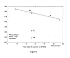
- Figure 1 is a graph of Si-N absorbance wavenumbers vs. flow ratio of additive (NH3, N2 or He) to aminosilane, BTBAS, under the conditions shown in the graph, where lower wavenumber equates to higher density.
- additive NH3, N2 or He
- Figure 2 is FTIR spectra of silicon nitride films grown by PECVD using BTBAS, under the conditions shown in the graph
- Figure 3 is FTIR spectra of silicon nitride films grown by PECVD using BIPAS, bis(isopropylamino)silane, under the conditions shown in the graph.
- Figure 4 shows film stresses related to different additives used to deposit PECVD films using BIPAS.
- Figure 5 compares etch rates of LPCVD and PECVD films as descibed in the graph.
- VLSI Very Large Scale Integration
- These deposited thin films can be of metals, semiconductors, or insulators.
- the films may be thermally grown or deposited from the vapor phase using LPCVD.
- VLSI technology requires very thin insulators for a variety of applications in both microprocessors and random-access memories device fabrication.
- Silicon dioxide has been predominantly used as a dielectric material because of its ease of deposition and excellent properties at the SiO 2 /Si interface.
- Silicon nitride has other advantages over silicon dioxide, some of these include impurity and dopant resistant diffusion barriers, high dielectric breakdown voltages, superior mechanical and inherent inertness of Si 3 N 4 .
- the present invention is directed to a class of aminosilanes that deposit silicon nitride at unexpectedly low temperatures with superior uniformities and high densities under plasma enhanced chemical vapor deposition when an ammonia reactant is increased or replaced with nitrogen, helium, argon or xenon.
- the aminosilane can include those structures set forth in Table 1 below.
- BDEAES Bis(diethylamino)ethylsilane
- BDEAS Bis(diethylamino)silane
- the mono-, bis-, tris-, and tetrakis- structures are also included.
- Bis(tertiarybutylamino)silane is particularly of interest and has the following formula: (t-C 4 H 9 NH) 2 Si(H) 2 .
- the deposited films have superior uniformities and are free of ammonium chloride and chlorine contamination.
- the bis(tertiarybutylamino)silane apparently has the property to deposit silicon nitride at 250-300°C below that of the dichlorosilane + ammonia process by LPCVD.
- aminosilanes such as; bis(tertiarybutylamino)silane
- N-Si bond may be attributable to the inherent property of the N-Si bond.
- the presence of the N-H bond may facilitate labile ⁇ -hydride transfer to form diaminosilane.
- the bis(tertiarybutylamino)silane and ammonia are allowed to react in the plasma to form precursors that result in silicon nitride depositions on a wafer at a wafer temperature of less than 500°C (preferably 420°C, but the temperature could be less or greater than this range). Reaction may occur either on the surface or very close to the wafer surface to deposit a thin silicon nitride film. If the reaction occurs in the gas phase (a homogeneous reaction) then clusters of silicon nitride are formed. Such cases are typical in silane and ammonia process. When the reaction occurs on the wafer surface, then the resulting films are of superior quality. Thus, one important requirement for a PECVD application is the degree to which heterogeneous reactions are favored over gas phase reactions.
- the PECVD process can be grouped into a) a gas-phase process and b) a surface reaction process.
- the gas phase phenomenon is the rate at which gases impinge on the substrate. This is modeled by the rate at which gases cross the boundary layer that separates the bulk regions of flowing gas and substrate surface. Such transport processes occur by gas-phase diffusion, which is proportional to the diffusivity of the gas and concentration gradient across the boundary layer.
- Several surface processes can be important when the gases reach the hot surface, but the surface reaction, in general, can be modeled by a thermally activated phenomenon which proceeds at a rate which is a function of the frequency factor, the activation energy, and the temperature.
- the surface reaction rate increases with increasing temperature.
- the temperature may rise high enough so that the reaction rate exceeds the rate at which reactant species arrive at the surface. In such cases, the reaction cannot proceed any more rapidly than the rate at which reactant gases are supplied to the substrate by mass transport. This is referred to as a mass-transport limited deposition process.
- the surface reaction rate is reduced, and eventually the concentration of reactants exceeds the rate at which they are consumed by the surface reaction process. Under such conditions the deposition rate is reaction rate limited.
- the deposition is usually mass-transport limited, while at lower temperatures it is surface-reaction rate-limited.
- the temperature at which the deposition condition moves from one of these growth regimes to the other is dependent on the activation energy of the reaction, and the gas flow conditions in the reactor. Thus, it is difficult to extrapolate process conditions or results from one pressure regime or temperature regime to another.
- the temperature of the process is an important parameter. That is, uniform deposition rates throughout a reactor require conditions that maintain a constant reaction rate. This, in turn, implies that a constant temperature must exist everywhere on all wafer surfaces. On the other hand, under such conditions, the rate at which reactants reach the surface is not important, since their concentration does not limit the growth rate. Thus, it is not as critical that a reactor be designed to supply an equal flux of reactants to all locations of a wafer surface.
- the vacuum system consisted of a rotary vane pump/roots blower combination and various traps.
- the reactor pressure is controlled by a capacitance manometer feedback to a throttle valve controller.
- Reactor loading was through a load-lock such that the reaction chamber was kept under vacuum at all times.
- the present invention of a method of depositing etch-resistant, low hydrogen silicon nitride films on silicon wafers by using a aminosilane precursor with increasing quantities of ammonia or replacing ammonia with nitrogen, argon, xenon or helium has been demonstrated experimentally.
- Bis(tertiarybutylamino)silane is a non-pyrophoric volatile liquid which is safer to handle than silane and dichlorosilane.
- the deposition process is carried out at preferably 20mTorr-2Torr in the temperature range of 200 to 500°C, preferably 420°C, using vapors from bis(tertiarybutylamino)silane and ammonia.
- an unreactive gas diluent such as nitrogen, helium, xenon or argon, can be used to dilute or replace the ammonia in order to achieve extremely high density silicon nitride films.
- the molar feed ratio of ammonia to bis(tertiarybutylamino)silane is preferably in the range of 18:1 to 33:1
- the process is performed in a cold wall PECVD reaction chamber.
- the process steps are as follows:
- Figure 1 is a graph of Si-N absorbance wavenumbers vs. flow ratio of additive (NH3, N2 or He) to aminosilane, BTBAS, under the conditions shown in the graph, where lower wavenumber equates to higher density.
- additive NH3, N2 or He
- Figure 2 is FTIR spectra of silicon nitride films grown by PECVD using BTBAS, under the conditions shown in the graph
- BIS(isopropylamino)silane is also non-pyrophoric volatile liquid which is safer to handle than silane and dichlorosilane.
- the process is identical to that in Example 1, except the precursor temperature is maintained at 40°C because of its higher vapor pressure than BTBAS.
- the results of the PECVD depositions are shown in Figure 3 under conditions given in the graph. For comparison of hydrogen concentrations, LPCVD films have approximately 3 atomic percent hydrogen.
- Figure 4 shows the film stress resulting from use of different additives. The stress may be modified by different combinations of additives.
- Etch rates are a measure of the film composition and density of the as deposited silicon nitride films.
- the data in Table 2 and Figure 5 demonstrates that the PECVD process of the present invention, using either increased ammonia reactant or replacing ammonia with an unreactive gas such as nitrogen or helium, and presumably, xenon or argon, results in very low etch rate silicon nitride films also.
- Such apparently high-density silicon nitride films with increased resistance to etch are highly desirable in the electronic device fabrication industry because silicon nitride is frequently used as an etch stop against metal and oxide films, so that differential etch rates facilitate fabrication of metal-oxide-semiconductor composites with appropriate patterning.
Abstract
Description
- The present invention is directed to the field of plasma enhanced low pressure chemical vapor deposition of silicon nitride films using aminosilanes, a range of ammonia or a relatively inert gas to improve the etch resistance and reduce the hydrogen concentration of the deposited silicon nitride.
- In the fabrication of semiconductor devices, a thin passive layer of a chemically inert dielectric material such as silicon nitride (Si3N4) is essential. Thin layers of silicon nitride function as diffusion masks, oxidation barriers, trench isolation, intermetallic dielectric material with high dielectric breakdown voltages and passivation layers. Many other applications of silicon nitride coatings in the fabrication of semiconductor devices are reported elsewhere, see Semiconductor and Process technology handbook, edited by Gary E. McGuire, Noyes Publication, New Jersey, (1988), pp 289-301; and Silicon Processing for the VLSI ERA, Wolf, Stanley, and Talbert, Richard N., Lattice Press, Sunset Beach, California (1990), pp 20-22, 327-330.
- The present semiconductor industry standard silicon nitride growth method is by low pressure chemical vapor deposition ("LPCVD") in a hot wall reactor at >750°C using dichlorosilane and ammonia.
- Deposition of silicon nitride over large numbers of silicon wafers has been accomplished using many precursors. The low pressure chemical vapor deposition using dichlorosilane and ammonia requires deposition temperatures greater than 750°C to obtain reasonable growth rates and uniformities. Higher deposition temperatures are typically employed to get the best film properties. There are several drawbacks in these processes and some of these are as follows:
- i) Deposition under 850°C gives poor hazy films with chlorine and particle contamination;
- ii) Silane and dichlorosilane are pyrophoric, toxic compressed gases;
- iii) Films formed from dichlorosilane result in the formation of less uniform films; and
- iv) Films from dichlorosilane have contaminants, such as chlorine and ammonium chloride, which are formed as byproducts.
- Japanese Patent 6-132284 describes deposition of silicon nitride using organosilanes with a general formula (R1R2N)n SiH4-n ( where R1 and R2 range from H-, CH3 -, C2H5- C3H7-, C4H9-) by a plasma enhanced chemical vapor deposition and thermal chemical vapor deposition in the presence of ammonia or nitrogen. The precursors described here are tertiary amines and do not contain NH bonding as in the case of the present invention. The deposition experiments were carried out in a single wafer reactor at 400°C at high pressures of 80-100 Torr. The Si:N ratios in these films were 0.9 (Si:N ratios in Si3N4 films is 0.75) with hydrogen content in the deposited films. The butyl radical is in the form of isobutyl.
- Sorita et al., J. Electro.Chem. Soc. , Vol 141, No12, (1994), pp 3505-3511, describe deposition of silicon nitride using dichlorosilane and ammonia using a LPCVD process. The major products in this process are aminochlorosilane, silicon nitride and ammonium chloride. Formation of ammonium chloride is a major drawback of using Si-Cl containing precursors. The formation of ammonium chloride leads to particle formation and deposition of ammonium chloride at the backend of the tube and in the plumbing lines and the pumping system. Processes which contain chlorine in the precursors result in NH4Cl formation. These processes require frequent cleaning and result in large down time of the reactors.
- B. A. Scott, J. M. Martnez-Duart, D.B. Beach, T. N. Nguyen, R. D. Estes and R.G. Schad., Chemtronics, 1989, Vol 4, pp 230-234., report deposition of silicon nitride using silane and ammonia by PECVD in the temperature region of 250-400°C. Silane is a pyrophoric gas and is difficult to control for the deposition of clean silicon nitride due to partial gas phase reaction.
- J. M. Grow, R. A. Levy, X. Fan and M. Bhaskaran, Materials Letters, 23, (1995), pp 187-193, describe deposition of silicon nitride using ditertiarybutylsilane and ammonia by LPCVD process in the temperature range of 600-700°C. The deposited silicon nitride films were contaminated with carbon impurities (10 atomic %). This is mainly due to the presence of direct Si-C bonds in the precursor.
- A. K. Hochberg and D. L. O'Meara, Mat. Res. Soc. Symp. Proc,. Vol. 204, (1991), pp 509-514, report deposition of silicon nitride and silicon oxynitride by using diethylsilane with ammonia and nitric oxide by LPCVD. The deposition was carried out in the temperature range of 650°C to 700°C. The deposition is limited to deposition at 650°C and the deposition rate drops to below 4Å/min at lower temperatures. In the LPCVD process, precursors which contain direct Si-C carbon bonds result in carbon contamination in the films. Carbon free deposition requires greater than 5:1 NH3 to precursor ratios. At lower ammonia concentrations, the films were found to contain carbon. Diethylsilane + ammonia processes typically require covered boats or temperature ramping to improve uniformities across the wafers.
- US Patent 5,234,869 and R.G. Gordon and D. M. Hoffman, Chem. Mater., Vol. 2, (1990), pp 482-484 disclose other attempts to reduce the amount of carbon involved aminosilanes, such as tetrakis(dimethylamino)silane. The temperature of deposition is in the range of 300-1000°C with pressures in the range of 1 mTorr-10 Torr. The presence of direct Si-N bonds and the absence of Si-C bonds were expected to give lower carbon concentrations in the films. However, there are three main disadvantages with precursors of this class.
- 1) They contain N-methyl groups, the methyl groups tend to migrate to the silicon surface readily and contaminate the films with carbon during a CVD process. In order to reduce the amount of carbon, the process involves high temperatures (>700) and high ammonia ratios (>10:1). With increased ammonia ratios the deposition rates dramatically reduce due to reactant depletion.
- 2) They do not contain NH bonding and they do not involve secondary silanes.
- 3) At lower temperatures the deposition rates and uniformities are very poor (>5%).
- US Patent 5,874,368 teaches the use of bis(tertiarybutylamino)silane as a precursor to deposit silicon nitride using low pressure chemical vapor deposition at a temperature range of 500° to 800° C. Ammonia, nitrogen and argon are considered for reaction atmospheres, with ammonia present at greater than 1:1 ratios of the aminosilane.
- US Patent 6,268,299 is directed to silicon nitride depositions using LPCVD, but makes the statement at col. 5, lines34-35; "Thus, the conventional PECVD process used to deposit nitride barrier films has a number of inherent disadvantages."
- US Patent 5,622,596 discloses at col. 3, lines 17-20 that silicon nitride stoichiometry can be related to silane and ammonia and nitrogen ratios in a plasma enhanced chemical vapor deposition ("PECVD") process.
- US Patent 5,040,046 reports that diethylsilane with nitrogen-containing or oxygen-containing compounds can create dense silicon nitride or silicon oxide, respectively, under PECVD conditions.
- The prior art has attempted to produce silicon nitride films at low temperatures, at high deposition rates and low hydrogen and carbon concentrations. The low hydrogen is required because
- Hydrogen migrates to the Si-SiO2 interface where it creates interface states (electrical instabilities)
- Hydrogen lowers film densities, thus increasing etch rates.
- Hydrogen decreases the thermal stability of deposited films.
- Film stresses change with hydrogen migration.
- However, the prior art has not been successful in achieving all these goals simultaneously with a silicon nitride precursor. The present invention has overcome the problems of the prior art with the use of aminosilanes in a PECVD process for the formation of silicon nitride which avoids the problems of the prior art, operates at low thermal conditions, avoids Si-C bonds to reduce carbon contamination of the resulting films, has low hydrogen concentrations, as well as avoiding chlorine contamination and operates at low pressures (20 mTorr - 2 Torr) in a manufacturable system as will be described in greater detail below.
- The present invention is a process for the plasma enhanced chemical vapor deposition of high density silicon nitride on a substrate using an aminosilane and a reactant selected from the group consisting of nitrogen, argon, xenon, helium and high ratios of ammonia in relation to the aminosilane.
- Figure 1 is a graph of Si-N absorbance wavenumbers vs. flow ratio of additive (NH3, N2 or He) to aminosilane, BTBAS, under the conditions shown in the graph, where lower wavenumber equates to higher density.
- Figure 2 is FTIR spectra of silicon nitride films grown by PECVD using BTBAS, under the conditions shown in the graph
- Figure 3 is FTIR spectra of silicon nitride films grown by PECVD using BIPAS, bis(isopropylamino)silane, under the conditions shown in the graph.
- Figure 4 shows film stresses related to different additives used to deposit PECVD films using BIPAS.
- Figure 5 compares etch rates of LPCVD and PECVD films as descibed in the graph.
- A large variety of "thin films" are used in the fabrication of Very Large Scale Integration (VLSI) devices. These deposited thin films can be of metals, semiconductors, or insulators. The films may be thermally grown or deposited from the vapor phase using LPCVD. VLSI technology requires very thin insulators for a variety of applications in both microprocessors and random-access memories device fabrication. Silicon dioxide has been predominantly used as a dielectric material because of its ease of deposition and excellent properties at the SiO2/Si interface. Silicon nitride has other advantages over silicon dioxide, some of these include impurity and dopant resistant diffusion barriers, high dielectric breakdown voltages, superior mechanical and inherent inertness of Si3N4.
- In VLSI fabrication a large set of rigorous chemical, structural, process and electrical requirements need to be satisfied. Purity of the film, thickness, uniformity and deposition rates are some of the strictly controlled parameters to facilitate fabrication of submicron features in a device. It is a major advantage in the fabrication and performance of a device if the deposition process can be carried out at temperatures lower than 500°C. A safe, reliable low temperature silicon nitride source material has applications in other technologies, such as; flat panel display devices, other electronic and non-electronic substrates or compound semiconductor device fabrication.
- The present invention is directed to a class of aminosilanes that deposit silicon nitride at unexpectedly low temperatures with superior uniformities and high densities under plasma enhanced chemical vapor deposition when an ammonia reactant is increased or replaced with nitrogen, helium, argon or xenon.
- The aminosilane can include those structures set forth in Table 1 below.

Where BTBAS = Bis(tertiarybutylamino)silane
TIPAS = Tris(isopropylamino)silane
BDEAES = Bis(diethylamino)ethylsilane
BDEAS = Bis(diethylamino)silane
TEAS = Tris(ethylamino)silane
or [(RxNH(2-x)]ySiH(3-y) where x= 1,2; y= 1,2,3; R=alkyl, aryl, arylalkyl, alkenyl or alkynyl. - The mono-, bis-, tris-, and tetrakis- structures are also included.
- Bis(tertiarybutylamino)silane is particularly of interest and has the following formula:
(t-C4H9NH)2Si(H)2.
- The deposited films have superior uniformities and are free of ammonium chloride and chlorine contamination. The bis(tertiarybutylamino)silane apparently has the property to deposit silicon nitride at 250-300°C below that of the dichlorosilane + ammonia process by LPCVD.
- The advantage of aminosilanes, such as; bis(tertiarybutylamino)silane, may be attributable to the inherent property of the N-Si bond. The presence of the N-H bond may facilitate labile β-hydride transfer to form diaminosilane.
- Other advantages of aminosilanes can be summarized as follows:
- 1) They are generally non-pyrophoric, volatile, stable liquids.
- 2) They do not have any chlorine in the precursor. The Si-Cl bonds in dichlorosilane leads to the formation of ammonium chloride, which deposits in the back end of the tube and requires frequent cleaning.
- 3) The precursors preferably do not contain direct Si-C bonds, and the resulting LPCVD silicon nitride films are carbon free, as indicated by auger spectroscopy.
- 4) The t-butyl amino ligands of bis(tertiarybutylamino)silane behave as good leaving groups to form isobutylene and are readily eliminated during pyrolysis. This is thought to be in part because the compound has a N-H bond. This additional advantage helps in removing all the carbon cleanly without contaminating the deposited films.
- 5) When compared to the dichlorosilane and ammonia process, aminosilane gives cleaner films at lower temperature.
- To form silicon nitride films by PECVD, the bis(tertiarybutylamino)silane and ammonia are allowed to react in the plasma to form precursors that result in silicon nitride depositions on a wafer at a wafer temperature of less than 500°C (preferably 420°C, but the temperature could be less or greater than this range). Reaction may occur either on the surface or very close to the wafer surface to deposit a thin silicon nitride film. If the reaction occurs in the gas phase (a homogeneous reaction) then clusters of silicon nitride are formed. Such cases are typical in silane and ammonia process. When the reaction occurs on the wafer surface, then the resulting films are of superior quality. Thus, one important requirement for a PECVD application is the degree to which heterogeneous reactions are favored over gas phase reactions.
- The PECVD process can be grouped into a) a gas-phase process and b) a surface reaction process. The gas phase phenomenon is the rate at which gases impinge on the substrate. This is modeled by the rate at which gases cross the boundary layer that separates the bulk regions of flowing gas and substrate surface. Such transport processes occur by gas-phase diffusion, which is proportional to the diffusivity of the gas and concentration gradient across the boundary layer. Several surface processes can be important when the gases reach the hot surface, but the surface reaction, in general, can be modeled by a thermally activated phenomenon which proceeds at a rate which is a function of the frequency factor, the activation energy, and the temperature.
- The surface reaction rate increases with increasing temperature. For a given surface reaction, the temperature may rise high enough so that the reaction rate exceeds the rate at which reactant species arrive at the surface. In such cases, the reaction cannot proceed any more rapidly than the rate at which reactant gases are supplied to the substrate by mass transport. This is referred to as a mass-transport limited deposition process. At lower temperatures, the surface reaction rate is reduced, and eventually the concentration of reactants exceeds the rate at which they are consumed by the surface reaction process. Under such conditions the deposition rate is reaction rate limited. Thus, at high temperatures, the deposition is usually mass-transport limited, while at lower temperatures it is surface-reaction rate-limited. In actual processes, the temperature at which the deposition condition moves from one of these growth regimes to the other is dependent on the activation energy of the reaction, and the gas flow conditions in the reactor. Thus, it is difficult to extrapolate process conditions or results from one pressure regime or temperature regime to another.
- In processes that are run under reaction rate-limited conditions, the temperature of the process is an important parameter. That is, uniform deposition rates throughout a reactor require conditions that maintain a constant reaction rate. This, in turn, implies that a constant temperature must exist everywhere on all wafer surfaces. On the other hand, under such conditions, the rate at which reactants reach the surface is not important, since their concentration does not limit the growth rate. Thus, it is not as critical that a reactor be designed to supply an equal flux of reactants to all locations of a wafer surface.
- To induce the low pressure conditions in the reactor, an appropriate vacuum system is necessary. For the present experiments, the vacuum system consisted of a rotary vane pump/roots blower combination and various traps. The reactor pressure is controlled by a capacitance manometer feedback to a throttle valve controller. Reactor loading was through a load-lock such that the reaction chamber was kept under vacuum at all times.
- The present invention of a method of depositing etch-resistant, low hydrogen silicon nitride films on silicon wafers by using a aminosilane precursor with increasing quantities of ammonia or replacing ammonia with nitrogen, argon, xenon or helium has been demonstrated experimentally.
- Bis(tertiarybutylamino)silane is a non-pyrophoric volatile liquid which is safer to handle than silane and dichlorosilane. The deposition process is carried out at preferably 20mTorr-2Torr in the temperature range of 200 to 500°C, preferably 420°C, using vapors from bis(tertiarybutylamino)silane and ammonia. Preferably, an unreactive gas diluent, such as nitrogen, helium, xenon or argon, can be used to dilute or replace the ammonia in order to achieve extremely high density silicon nitride films. The molar feed ratio of ammonia to bis(tertiarybutylamino)silane is preferably in the range of 18:1 to 33:1
- The process is performed in a cold wall PECVD reaction chamber. The process steps are as follows:
- 1. The susceptor is maintained at approximately 420 °C.
- 2. The silicon substrate is placed on the susceptor and sufficient time is given to reach the susceptor temperature.
- 3. Nitrogen or helium gas is introduced to the reaction chamber at 10 sccm.
- 4. Reaction chamber pressure is set to 1 Torr.
- 5. RF power density of 0.65 W/cm2 is applied to the electrodes.
- 6. Ammonia and BTBAS are introduced to the reaction chamber at an ammonia :
BTBAS flow ratio of greater than 5:1; preferably in the range of 18:1 to 33:1 - 7. Nitrogen, argon, xenon or helium may be used in place of ammonia in step 6.
- 8. The BTBAS vapor flow rate is approximately 11 sccm.
- 9. The BTBAS source temperature is 55 °C.
- 10. After the deposition, the substrate are removed through a loadlock and the film properties are measured.
- Figure 1 is a graph of Si-N absorbance wavenumbers vs. flow ratio of additive (NH3, N2 or He) to aminosilane, BTBAS, under the conditions shown in the graph, where lower wavenumber equates to higher density.
- Figure 2 is FTIR spectra of silicon nitride films grown by PECVD using BTBAS, under the conditions shown in the graph
- BIS(isopropylamino)silane is also non-pyrophoric volatile liquid which is safer to handle than silane and dichlorosilane. The process is identical to that in Example 1, except the precursor temperature is maintained at 40°C because of its higher vapor pressure than BTBAS. The results of the PECVD depositions are shown in Figure 3 under conditions given in the graph. For comparison of hydrogen concentrations, LPCVD films have approximately 3 atomic percent hydrogen. Figure 4 shows the film stress resulting from use of different additives. The stress may be modified by different combinations of additives.
- In general, silicon nitride etch resistance increases with ammonia flow contrary to LPCVD results (Figure 5). More etch resistant and lower hydrogen concentration films are obtained by replacing ammonia with nitrogen, Significant improvements are achieved, further, by using an inert gas in place of nitrogen. Having the nitrogen in the film coming only from the aminosilane shifts the Si-N absorption wavelength to lower wavenumbers, indicative of denser bonding. Also, in Figure 4 it is seen that PECVD films with nitrogen have the etch resistance of LPCVD films grown at much higher temperatures (550°C). Further, using an inert gas in place of nitrogen results in film etch resistances equivalent to 600°C LPCVD films. Although, the graph shows results for 1 % HF, similar results are obtained using buffered HF mixtures (Dil BOE) as shown in Table 2.
- Etch rates are a measure of the film composition and density of the as deposited silicon nitride films. The data in Table 2 and Figure 5 demonstrates that the PECVD process of the present invention, using either increased ammonia reactant or replacing ammonia with an unreactive gas such as nitrogen or helium, and presumably, xenon or argon, results in very low etch rate silicon nitride films also. Such apparently high-density silicon nitride films with increased resistance to etch are highly desirable in the electronic device fabrication industry because silicon nitride is frequently used as an etch stop against metal and oxide films, so that differential etch rates facilitate fabrication of metal-oxide-semiconductor composites with appropriate patterning.
TABLE 2 Wafer # Dep Type Temp °C Source NH3 ratio Relative Etch Rate 1% HFRelative Etch Rate Dil BOE Thermal Ox# 1Growth 1000 na na 1.00 - Thermal Ox# 2Growth 1000 na na 1.00 - Thermal Ox# 3Growth 1000 na na - 1.00 Thermal Ox#4 Growth 1000 na na - 1.00 1427-141C PECVD 420 BTBAS 18 31.99 - 1427-142C PECVD 420 BTBAS 26 15.12 - 1427-143C PECVD 420 BTBAS 33 8.84 - 1427-136 PECVD 420 BTBAS N2 0.21 - bipas-8 PECVD 420 BIPAS N2 0.23 - 1427-137 PECVD 420 BTBAS He 0.06 - bipas-5 PECVD 420 BIPAS He 0.06 0.04 BTBAS-P5 PECVD 420 BTBAS He - 0.03 bipas-11 PECVD 420 BIPAS He - 0.02 BTBAS-P14 PECVD 375 BTBAS 50 - 4.44 BTBAS-P25 PECVD 350 BTBAS 50 - 6.91 BTBAS-P18 PECVD 350 BTBAS He - 0.07 2773N25 LPCVD 550 BTBAS 1 0.12 - 2776N25 LPCVD 550 BTBAS 1.5 0.15 - 2772N25 LPCVD 550 BTBAS 2 0.20 - ATV-130-02 LPCVD 570 BTBAS 2 - 0.07 ATV-53-24 LPCVD 600 BTBAS 2 0.05 0.02 ATV-36-24 LPCVD 600 BTBAS 3 0.07 0.03 NOTE: Etch rate of thermal depositions increases with ammonia ratio, while increasing ammonia for PECVD decreases the etch rate. - The present invention has been described with regard to a preferred embodiment, however the full scope of the present invention should be ascertained from the claims which follow.
Claims (18)
- A process for decreasing the wet etch rate of plasma enhanced chemical vapor deposition silicon nitride on a substrate using a silicon precursor having at least one Si-N bond and a reagent selected from the group consisting of: (i) nitrogen; (ii) argon; (iii) xenon; (iv) helium; (v) mixtures of (ii), (iii) and/or (iv); (vi) ammonia and/or hydrazine; and (vii) the combination of an inert gas of (ii), (iii), (iv) or (v) with less than 1% ammonia in relation to the inert gas.
- The process of Claim 1 wherein the silicon precursor has the formula:
(t-C4H9NH)2SiH2.
- The process of Claim 1 wherein the temperature of the substrate is less than 800°C.
- The process of Claim 1 wherein the temperature of the substrate is less than 500°C.
- The process of Claim 1 wherein the pressure is at least approximately 1 mTorr.
- The process of Claim 1 wherein the reagent is nitrogen.
- The process of Claim 1 wherein the reactant is helium.
- The process of Claim 1 wherein the reactant is ammonia and/or hydrazine.
- The process of Claim 1 wherein the substrate is selected from the group consisting of silicon, silicon dioxide or a metal.
- The process of Claim 1 wherein the substrate is an electronic device.
- The process of Claim 1 wherein the substrate is a flat panel display.
- A plasma enhanced chemical vapor deposition of low etch rate, low hydrogen content silicon nitride in a reaction zone, comprising the steps of:a) heating a substrate to a temperature less than or equal to 800°C in said zone;b) maintaining the substrate in a vacuum at a pressure at least approximately 1 mTorr in said zone;c) introducing into said zone a silicon precursor of the formula:
(t-C4H9NH)2SiH2 and a reagent selected from the group consisting of (i) nitrogen; (ii) argon; (iii) xenon; (iv) helium; (v) mixtures of (ii), (iii) and/or (iv); (vi) ammonia and/or hydrazine; and (vii) the combination of an inert gas of (ii), (iii), (iv) or (v) with less than 1% ammonia in relation to the inert gas; andd) maintaining the conditions of a) through c) sufficient to cause a film of low etch rate, low hydrogen content silicon nitride to deposit on the substrate. - A plasma enhanced chemical vapor deposition of high density silicon nitride in a reaction zone, comprising the steps of:a) heating a substrate to a temperature less than or equal to 500°C in said zone;b) maintaining the substrate in a vacuum at a pressure at least approximately 1 mTorr in said zone;c) introducing into said zone a silicon precursor of the formula: (t-C4H9NH)2SiH2 and nitrogen; andd) maintaining the conditions of a) through c) sufficient to cause a film of low etch rate, low hydrogen content silicon nitride to deposit on the substrate.
- A plasma enhanced chemical vapor deposition of dense silicon nitride in a reaction zone, comprising the steps of:a) heating a substrate to a temperature less than or equal to 500°C in said zone;b) maintaining the substrate in a vacuum at a pressure at least approximately 1 mTorr in said zone;c) introducing into said zone a silicon precursor of the formula: (t-C4H9NH)2SiH2 and helium; andd) maintaining the conditions of a) through c) sufficient to cause a film of low etch rate, low hydrogen content silicon nitride to deposit on the substrate.
- A plasma enhanced chemical vapor deposition of low etch rate, low hydrogen content silicon nitride in a reaction zone, comprising the steps of:a) heating a substrate to a temperature less than or equal to 500°C in said zone;b) maintaining the substrate in a vacuum at a pressure at least approximately 1 mTorr in said zone;c) introducing into said zone a silicon precursor of the formula:
(t-C4H9NH)2SiH2 and an inert gas selected from the group consisting of: argon, xenon, helium and mixtures thereof; with less than 1% ammonia in relation to the inert gas; andd) maintaining the conditions of a) through c) sufficient to cause a film of low etch rate, low hydrogen content silicon nitride to deposit on the substrate. - A process for producing a silicon nitride film of reduced etch rate on a substrate, comprising; conducting a plasma enhanced chemical vapor deposition of an aminosilane and a reagent selected from the group consisting of: (i) nitrogen; (ii) argon; (iii) xenon; (iv) helium; (v) mixtures of (ii), (iii) and/or (iv); (vi) ammonia and/or hydrazine; and (vii) the combination of an inert gas of (ii), (iii), (iv) or (v) with less than 1% ammonia in relation to the inert gas.
- A process for producing a silicon nitride film of reduced etch rate using plasma enhanced chemical vapor deposition of low etch rate, low hydrogen content silicon nitride in a reaction zone, comprising the steps of:a) heating a substrate to a temperature less than or equal to 500°C in said zone;b) maintaining the substrate in a vacuum at a pressure in the range of approximately 20mTorr-2Torr in said zone;c) introducing into said zone an aminosilane of the formula: [(RxNH(2-x)]ySiH(3-y) where x= 1,2; y= 1,2,3; R=alkyl, aryl, arylalkyl, alkenyl or alkynyl and a reagent selected from the group consisting of (i) nitrogen; (ii) argon; (iii) xenon; (iv) helium; (v) mixtures of (ii), (iii) and/or (iv); (vi) ammonia and/or hydrazine; and (vii) the combination of an inert gas of (ii), (iii), (iv) or (v) with less than 1% ammonia in relation to the inert gas; andd) maintaining the conditions of a) through c) sufficient to cause a film of low etch rate, low hydrogen content silicon nitride to deposit on the substrate.
- A process for the plasma enhanced chemical vapor deposition of low etch rate, low hydrogen content silicon nitride on a substrate using an aminosilane and a reactant selected from the group consisting of nitrogen, argon, xenon, helium and 18:1 to 33:1 ammonia in relation to the aminosilane.
Applications Claiming Priority (1)
| Application Number | Priority Date | Filing Date | Title |
|---|---|---|---|
| US10/929,755 US20060045986A1 (en) | 2004-08-30 | 2004-08-30 | Silicon nitride from aminosilane using PECVD |
Publications (2)
| Publication Number | Publication Date |
|---|---|
| EP1630249A2 true EP1630249A2 (en) | 2006-03-01 |
| EP1630249A3 EP1630249A3 (en) | 2006-07-12 |
Family
ID=35478643
Family Applications (1)
| Application Number | Title | Priority Date | Filing Date |
|---|---|---|---|
| EP05018682A Withdrawn EP1630249A3 (en) | 2004-08-30 | 2005-08-29 | Process for chemical vapor deposition of silicon nitride. |
Country Status (4)
| Country | Link |
|---|---|
| US (1) | US20060045986A1 (en) |
| EP (1) | EP1630249A3 (en) |
| IL (1) | IL170744A0 (en) |
| TW (1) | TW200713427A (en) |
Cited By (4)
| Publication number | Priority date | Publication date | Assignee | Title |
|---|---|---|---|---|
| EP2192207A1 (en) | 2008-11-12 | 2010-06-02 | Air Products And Chemicals, Inc. | Amino vinylsilane precursors for the deposition of intrinsically compressively stressed SiN films |
| EP2193541A1 (en) * | 2007-09-18 | 2010-06-09 | L'AIR LIQUIDE, Société Anonyme pour l'Etude et l'Exploitation des Procédés Georges Claude | Method of forming silicon-containing films |
| WO2013134661A1 (en) * | 2012-03-09 | 2013-09-12 | Air Products And Chemicals, Inc. | Barrier materials for display devices |
| US8889235B2 (en) | 2009-05-13 | 2014-11-18 | Air Products And Chemicals, Inc. | Dielectric barrier deposition using nitrogen containing precursor |
Families Citing this family (17)
| Publication number | Priority date | Publication date | Assignee | Title |
|---|---|---|---|---|
| US20060172556A1 (en) * | 2005-02-01 | 2006-08-03 | Texas Instruments Incorporated | Semiconductor device having a high carbon content strain inducing film and a method of manufacture therefor |
| US20060205192A1 (en) * | 2005-03-09 | 2006-09-14 | Varian Semiconductor Equipment Associates, Inc. | Shallow-junction fabrication in semiconductor devices via plasma implantation and deposition |
| US20080207007A1 (en) | 2007-02-27 | 2008-08-28 | Air Products And Chemicals, Inc. | Plasma Enhanced Cyclic Chemical Vapor Deposition of Silicon-Containing Films |
| US8987039B2 (en) * | 2007-10-12 | 2015-03-24 | Air Products And Chemicals, Inc. | Antireflective coatings for photovoltaic applications |
| US7678715B2 (en) * | 2007-12-21 | 2010-03-16 | Applied Materials, Inc. | Low wet etch rate silicon nitride film |
| US8129555B2 (en) * | 2008-08-12 | 2012-03-06 | Air Products And Chemicals, Inc. | Precursors for depositing silicon-containing films and methods for making and using same |
| US8912353B2 (en) | 2010-06-02 | 2014-12-16 | Air Products And Chemicals, Inc. | Organoaminosilane precursors and methods for depositing films comprising same |
| US8771807B2 (en) | 2011-05-24 | 2014-07-08 | Air Products And Chemicals, Inc. | Organoaminosilane precursors and methods for making and using same |
| EP3330404B1 (en) | 2011-06-03 | 2021-09-29 | Versum Materials US, LLC | Compositions and processes for depositing carbon-doped siliconcontaining films |
| KR20150034123A (en) | 2012-07-20 | 2015-04-02 | 레르 리키드 쏘시에떼 아노님 뿌르 레뜌드 에렉스뿔라따시옹 데 프로세데 조르즈 클로드 | Organosilane precursors for ald/cvd silicon-containing film applications |
| US9018108B2 (en) | 2013-01-25 | 2015-04-28 | Applied Materials, Inc. | Low shrinkage dielectric films |
| TW201509799A (en) | 2013-07-19 | 2015-03-16 | Air Liquide | Hexacoordinate silicon-containing precursors for ALD/CVD silicon-containing film applications |
| US9382268B1 (en) | 2013-07-19 | 2016-07-05 | American Air Liquide, Inc. | Sulfur containing organosilane precursors for ALD/CVD silicon-containing film applications |
| US10280084B2 (en) | 2013-11-28 | 2019-05-07 | Spp Technologies Co., Ltd. | Silicon nitride film and method of making thereof |
| US9912314B2 (en) * | 2014-07-25 | 2018-03-06 | Akoustics, Inc. | Single crystal acoustic resonator and bulk acoustic wave filter |
| US10570513B2 (en) | 2014-12-13 | 2020-02-25 | American Air Liquide, Inc. | Organosilane precursors for ALD/CVD silicon-containing film applications and methods of using the same |
| US10658296B2 (en) | 2016-09-30 | 2020-05-19 | Taiwan Semiconductor Manufacturing Co., Ltd. | Dielectric film for semiconductor fabrication |
Citations (6)
| Publication number | Priority date | Publication date | Assignee | Title |
|---|---|---|---|---|
| US5040046A (en) | 1990-10-09 | 1991-08-13 | Micron Technology, Inc. | Process for forming highly conformal dielectric coatings in the manufacture of integrated circuits and product produced thereby |
| US5234869A (en) | 1990-06-28 | 1993-08-10 | Kabushiki Kaisha Toshiba | Method of manufacturing silicon nitride film |
| JPH06132284A (en) | 1992-10-22 | 1994-05-13 | Kawasaki Steel Corp | Method for forming protective film of semiconductor device |
| US5622596A (en) | 1995-05-08 | 1997-04-22 | International Business Machines Corporation | High density selective SiO2 :Si3 N4 etching using a stoichiometrically altered nitride etch stop |
| US5874368A (en) | 1997-10-02 | 1999-02-23 | Air Products And Chemicals, Inc. | Silicon nitride from bis(tertiarybutylamino)silane |
| US6268299B1 (en) | 2000-09-25 | 2001-07-31 | International Business Machines Corporation | Variable stoichiometry silicon nitride barrier films for tunable etch selectivity and enhanced hyrogen permeability |
Family Cites Families (9)
| Publication number | Priority date | Publication date | Assignee | Title |
|---|---|---|---|---|
| FR2371777A1 (en) * | 1976-11-18 | 1978-06-16 | Loic Henry | METHOD OF MANUFACTURING A SILICON NITRIDE DIFFUSION BARRIER ON A SEMICONDUCTOR SUBSTRATE, IN PARTICULAR OF THE III-V TYPE |
| US4608096A (en) * | 1983-04-04 | 1986-08-26 | Monsanto Company | Gettering |
| US5935638A (en) * | 1998-08-06 | 1999-08-10 | Dow Corning Corporation | Silicon dioxide containing coating |
| JP2002063985A (en) * | 2000-08-22 | 2002-02-28 | Nec Corp | Organic electroluminescence element |
| US6500772B2 (en) * | 2001-01-08 | 2002-12-31 | International Business Machines Corporation | Methods and materials for depositing films on semiconductor substrates |
| JP2003166060A (en) * | 2001-11-30 | 2003-06-13 | L'air Liquide Sa Pour L'etude & L'exploitation Des Procede S Georges Claude | Method for manufacturing silicon nitride film, silicon oxynitride film, or silicon oxide film by cvd method |
| US6812073B2 (en) * | 2002-12-10 | 2004-11-02 | Texas Instrument Incorporated | Source drain and extension dopant concentration |
| US7001844B2 (en) * | 2004-04-30 | 2006-02-21 | International Business Machines Corporation | Material for contact etch layer to enhance device performance |
| US7049200B2 (en) * | 2004-05-25 | 2006-05-23 | Applied Materials Inc. | Method for forming a low thermal budget spacer |
-
2004
- 2004-08-30 US US10/929,755 patent/US20060045986A1/en not_active Abandoned
-
2005
- 2005-08-29 EP EP05018682A patent/EP1630249A3/en not_active Withdrawn
- 2005-09-08 IL IL170744A patent/IL170744A0/en unknown
- 2005-09-14 TW TW094131707A patent/TW200713427A/en unknown
Patent Citations (6)
| Publication number | Priority date | Publication date | Assignee | Title |
|---|---|---|---|---|
| US5234869A (en) | 1990-06-28 | 1993-08-10 | Kabushiki Kaisha Toshiba | Method of manufacturing silicon nitride film |
| US5040046A (en) | 1990-10-09 | 1991-08-13 | Micron Technology, Inc. | Process for forming highly conformal dielectric coatings in the manufacture of integrated circuits and product produced thereby |
| JPH06132284A (en) | 1992-10-22 | 1994-05-13 | Kawasaki Steel Corp | Method for forming protective film of semiconductor device |
| US5622596A (en) | 1995-05-08 | 1997-04-22 | International Business Machines Corporation | High density selective SiO2 :Si3 N4 etching using a stoichiometrically altered nitride etch stop |
| US5874368A (en) | 1997-10-02 | 1999-02-23 | Air Products And Chemicals, Inc. | Silicon nitride from bis(tertiarybutylamino)silane |
| US6268299B1 (en) | 2000-09-25 | 2001-07-31 | International Business Machines Corporation | Variable stoichiometry silicon nitride barrier films for tunable etch selectivity and enhanced hyrogen permeability |
Non-Patent Citations (7)
| Title |
|---|
| "SEMICONDUCTOR AND PROCESS TECHNOLOGY HANDBOOK", 1988, NOYES PUBLICATION, pages: 289 - 301 |
| "SILICON PROCESSING FOR THE VLSI ERA", 1990, LATTICE PRESS, pages: 20 - 22 |
| A. K. HOCHBERG; D. L. O'MEARA, MAT. RES. SOC. SYMP. PROC, vol. 204, 1991, pages 509 - 514 |
| B. A. SCOTT ET AL., CHEMTRONICS, vol. 4, 1989, pages 230 - 234 |
| J. M. GROW ET AL., MATERIALS LETTERS, vol. 23, 1995, pages 187 - 193 |
| R.G. GORDON; D. M. HOFFMAN, CHEM. MATER., vol. 2, 1990, pages 482 - 484 |
| SORITA, J. ELECTRO.CHEM. SOC., vol. 141, no. 12, 1994, pages 3505 - 3511 |
Cited By (7)
| Publication number | Priority date | Publication date | Assignee | Title |
|---|---|---|---|---|
| EP2193541A1 (en) * | 2007-09-18 | 2010-06-09 | L'AIR LIQUIDE, Société Anonyme pour l'Etude et l'Exploitation des Procédés Georges Claude | Method of forming silicon-containing films |
| EP2192207A1 (en) | 2008-11-12 | 2010-06-02 | Air Products And Chemicals, Inc. | Amino vinylsilane precursors for the deposition of intrinsically compressively stressed SiN films |
| EP2465861A1 (en) | 2008-11-12 | 2012-06-20 | Air Products and Chemicals, Inc. | Amino vinylsilane precursors for compressively stressed SiN films |
| US8580993B2 (en) | 2008-11-12 | 2013-11-12 | Air Products And Chemicals, Inc. | Amino vinylsilane precursors for stressed SiN films |
| US8889235B2 (en) | 2009-05-13 | 2014-11-18 | Air Products And Chemicals, Inc. | Dielectric barrier deposition using nitrogen containing precursor |
| WO2013134661A1 (en) * | 2012-03-09 | 2013-09-12 | Air Products And Chemicals, Inc. | Barrier materials for display devices |
| US10319862B2 (en) | 2012-03-09 | 2019-06-11 | Versum Materials Us, Llc | Barrier materials for display devices |
Also Published As
| Publication number | Publication date |
|---|---|
| TW200713427A (en) | 2007-04-01 |
| EP1630249A3 (en) | 2006-07-12 |
| IL170744A0 (en) | 2009-02-11 |
| US20060045986A1 (en) | 2006-03-02 |
Similar Documents
| Publication | Publication Date | Title |
|---|---|---|
| EP1630249A2 (en) | Process for chemical vapor deposition of silicon nitride. | |
| EP0906965B1 (en) | Silicon nitride from bis (tertiarybutylamino) silane | |
| EP0964441B1 (en) | Deposition of silicon dioxide and silicon oxynitride using bis(tertiarybutylamino)silane | |
| US7288145B2 (en) | Precursors for depositing silicon containing films | |
| US5204141A (en) | Deposition of silicon dioxide films at temperatures as low as 100 degree c. by lpcvd using organodisilane sources | |
| EP2644609B1 (en) | Precursors for depositing silicon-containing films and methods of using same | |
| US5744196A (en) | Low temperature deposition of silicon dioxide using organosilanes | |
| US7365029B2 (en) | Method for silicon nitride chemical vapor deposition | |
| US20050181633A1 (en) | Precursors for depositing silicon-containing films and processes thereof | |
| US20050227017A1 (en) | Low temperature deposition of silicon nitride | |
| EP1724373A1 (en) | Precursors for cvd silicon carbo-nitride films | |
| TW200422424A (en) | Low temperature deposition of silicon oxides and oxynitrides | |
| JP2005534173A (en) | Metal / organic chemical vapor deposition and atomic layer deposition of metal oxynitrides and metal silicon oxynitrides | |
| TWI246719B (en) | Low temperature deposition of silicon nitride | |
| KR20050020758A (en) | Metal organic chemical vapor deposition and atomic layer deposition of metal oxynitride and metal silicon oxynitride |
Legal Events
| Date | Code | Title | Description |
|---|---|---|---|
| PUAI | Public reference made under article 153(3) epc to a published international application that has entered the european phase |
Free format text: ORIGINAL CODE: 0009012 |
|
| AK | Designated contracting states |
Kind code of ref document: A2 Designated state(s): AT BE BG CH CY CZ DE DK EE ES FI FR GB GR HU IE IS IT LI LT LU LV MC NL PL PT RO SE SI SK TR |
|
| AX | Request for extension of the european patent |
Extension state: AL BA HR MK YU |
|
| PUAL | Search report despatched |
Free format text: ORIGINAL CODE: 0009013 |
|
| AK | Designated contracting states |
Kind code of ref document: A3 Designated state(s): AT BE BG CH CY CZ DE DK EE ES FI FR GB GR HU IE IS IT LI LT LU LV MC NL PL PT RO SE SI SK TR |
|
| AX | Request for extension of the european patent |
Extension state: AL BA HR MK YU |
|
| AKX | Designation fees paid | ||
| STAA | Information on the status of an ep patent application or granted ep patent |
Free format text: STATUS: THE APPLICATION IS DEEMED TO BE WITHDRAWN |
|
| 18D | Application deemed to be withdrawn |
Effective date: 20070113 |
|
| REG | Reference to a national code |
Ref country code: DE Ref legal event code: 8566 |