EP1640778A1 - System and method of reducing color shift in a display - Google Patents
System and method of reducing color shift in a display Download PDFInfo
- Publication number
- EP1640778A1 EP1640778A1 EP05255711A EP05255711A EP1640778A1 EP 1640778 A1 EP1640778 A1 EP 1640778A1 EP 05255711 A EP05255711 A EP 05255711A EP 05255711 A EP05255711 A EP 05255711A EP 1640778 A1 EP1640778 A1 EP 1640778A1
- Authority
- EP
- European Patent Office
- Prior art keywords
- optical element
- display system
- substrate
- axis
- forming
- Prior art date
- Legal status (The legal status is an assumption and is not a legal conclusion. Google has not performed a legal analysis and makes no representation as to the accuracy of the status listed.)
- Withdrawn
Links
Images


Classifications
-
- G—PHYSICS
- G02—OPTICS
- G02B—OPTICAL ELEMENTS, SYSTEMS OR APPARATUS
- G02B26/00—Optical devices or arrangements for the control of light using movable or deformable optical elements
- G02B26/08—Optical devices or arrangements for the control of light using movable or deformable optical elements for controlling the direction of light
-
- G—PHYSICS
- G02—OPTICS
- G02B—OPTICAL ELEMENTS, SYSTEMS OR APPARATUS
- G02B26/00—Optical devices or arrangements for the control of light using movable or deformable optical elements
- G02B26/001—Optical devices or arrangements for the control of light using movable or deformable optical elements based on interference in an adjustable optical cavity
-
- G—PHYSICS
- G02—OPTICS
- G02B—OPTICAL ELEMENTS, SYSTEMS OR APPARATUS
- G02B26/00—Optical devices or arrangements for the control of light using movable or deformable optical elements
Definitions
- the field of the invention relates to microelectromechanical systems (MEMS).
- MEMS microelectromechanical systems
- Microelectromechanical systems include micro mechanical elements, actuators, and electronics. Micromechanical elements may be created using deposition, etching, and or other micromachining processes that etch away parts of substrates and/or deposited material layers or that add layers to form electrical and electromechanical devices.
- An interferometric modulator may comprise a pair of conductive plates, one or both of which may be transparent and/or reflective in whole or part and capable of relative motion upon application of an appropriate electrical signal.
- One plate may comprise a stationary layer deposited on a substrate, the other plate may comprise a metallic membrane separated from the stationary layer by an air gap.
- Such devices have a wide range of applications, and it would be beneficial in the art to utilize and/or modify the characteristics of these types of devices so that their features can be exploited in improving existing products and creating new products that have not yet been developed.
- One embodiment is a display system for displaying an image.
- the display system includes a plurality of interferometric modulators configured to modulate light incident on a surface thereof.
- the display system further includes a converging optical element positioned with respect to a surface of at least one of the plurality of interferometric modulators such that a focal length of the optical element is greater than a distance between the optical element and the surface.
- Another embodiment is a method of fabricating a display system.
- the method includes forming a plurality of interferometric modulators on a first substrate.
- the method further includes forming a converging optical element on a second substrate.
- the optical element is positioned with respect to at least one surface of at least one of the plurality of interferometric modulators such that a focal length of the optical element is greater than a distance between the optical element and the at least one surface.
- Another embodiment is a display system fabricated according to this method.
- the display system includes means for interferometrically modulating light incident thereon and means for converging light adapted so as to limit color shift of at least a portion of the image between different viewing locations.
- Another embodiment is a method of fabricating a display system comprising: forming a plurality of interferometric modulators on a first substrate; and forming a converging diffractive optical element on a second substrate, the optical element positioned so as to redirect light that is incident on at least one surface of at least one of the plurality of interferometric modulators.
- Another embodiment is a display system for displaying an image, the display system comprising: means for interferometrically modulating light incident thereon; and means for diffracting light to redirect light incident on said means for interferometrically modulating light, wherein said means for diffracting light is configured to converge said light.
- Another embodiment is a display system for displaying an image, the display system comprising: a plurality of interferometric modulators configured to modulate light incident thereon; and a converging diffractive optical element configured to redirect light incident on at least one of the plurality of interferometric modulators.
- Another embodiment is a display system for displaying an image, the display system comprising: means for interferometrically modulating light incident thereon; and means for diffracting light to redirect light incident on said means for interferometrically modulating light.
- the invention includes an optical element, such as a lens, fresnel lens, diffractive optical element, or binary optical element, positioned between an interferometric display and a viewer of the display.
- the optical element is configured to reduce color shift that may be seen as the viewing angle or light angle changes.
- the following detailed description is directed to certain specific embodiments of the invention. However, the invention can be embodied in a multitude of different ways. In this description, reference is made to the drawings wherein like parts are designated with like numerals throughout. As will be apparent from the following description, the invention may be implemented in any device that is configured to display an image, whether in motion (e.g., video) or stationary (e.g., still image), and whether textual or pictorial.
- motion e.g., video
- stationary e.g., still image
- the invention may be implemented in or associated with a variety of electronic devices such as, but not limited to, mobile telephones, wireless devices, personal data assistants (PDAs), handheld or portable computers, GPS receivers/navigators, cameras, MP3 players, camcorders, game consoles, wrist watches, clocks, calculators, television monitors, flat panel displays, computer monitors, auto displays (e.g., odometer display, etc.), cockpit controls and/or displays, display of camera views (e.g., display of a rear view camera in a vehicle), electronic photographs, electronic billboards or signs, projectors, architectural structures, packaging, and aesthetic structures (e.g., display of images on a piece of jewelry).
- MEMS devices of similar structure to those described herein can also be used in non-display applications such as in electronic switching devices.
- interferometric modulator display embodiment comprising an interferometric MEMS display element is illustrated in Figure 1.
- the pixels are in either a bright or dark state.
- the display element In the bright ("on” or “open") state, the display element reflects a large portion of incident visible light to a user.
- the dark (“off” or “closed”) state When in the dark (“off” or “closed”) state, the display element reflects little incident visible light to the user.
- the light reflectance properties of the "on” and "off” states may be reversed.
- MEMS pixels can be configured to reflect predominantly at selected colors, allowing for a color display in addition to black and white.
- Figure 1 is an isometric view depicting two adjacent pixels in a series of pixels of a visual display, wherein each pixel comprises a MEMS interferometric modulator.
- an interferometric modulator display comprises a row/column array of these interferometric modulators.
- Each interferometric modulator includes a pair of reflective layers positioned at a variable and controllable distance from each other to form a resonant optical cavity with at least one variable dimension.
- one of the reflective layers may be moved between two positions. In the first position, referred to herein as the released state, the movable layer is positioned at a relatively large distance from a fixed partially reflective layer.
- the movable layer In the second position, the movable layer is positioned more closely adjacent to the partially reflective layer. Incident light that reflects from the two layers interferes constructively or destructively depending on the position of the movable reflective layer, producing either an overall reflective or non-reflective state for each pixel.
- the depicted portion of the pixel array in Figure 1 includes two adjacent interferometric modulators 12a and 12b.
- a movable and highly reflective layer 14a is illustrated in a released position at a predetermined distance from a fixed partially reflective layer 16a.
- the movable highly reflective layer 14b is illustrated in an actuated position adjacent to the fixed partially reflective layer 16b.
- the fixed layers 16a, 16b are electrically conductive, partially transparent and partially reflective, and may be fabricated, for example, by depositing one or more layers each of chromium and indium-tin-oxide onto a transparent substrate 20. The layers are patterned into parallel strips, and may form row electrodes in a display device as described further below.
- the movable layers 14a, 14b may be formed as a series of parallel strips of a deposited metal layer or layers (orthogonal to the row electrodes 16a, 16b) deposited on top of posts 18 and an intervening sacrificial material deposited between the posts 18. When the sacrificial material is etched away, the deformable metal layers are separated from the fixed metal layers by a defined air gap 19.
- a highly conductive and reflective material such as aluminum may be used for the deformable layers, and these strips may form column electrodes in a display device.
- the cavity 19 remains between the layers 14a, 16a and the deformable layer is in a mechanically relaxed state as illustrated by the pixel 12a in Figure1.
- a potential difference is applied to a selected row and column, the capacitor formed at the intersection of the row and column electrodes at the corresponding pixel becomes charged, and electrostatic forces pull the electrodes together.
- the movable layer is deformed and is forced against the fixed layer (a dielectric material which is not illustrated in this Figure may be deposited on the fixed layer to prevent shorting and control the separation distance) as illustrated by the pixel 12b on the right in Figure 1.
- the behavior is the sameregardless of the polarity of the applied potential difference. In this way, row/column actuation that can control the reflective vs. non-reflective pixel states is analogous in many ways to that used in conventional LCD and other display technologies.
- Figures 2 through 5 illustrate one exemplary process and system for using an array of interferometric modulators in a display application.
- Figure 2 is a system block diagram illustrating one embodiment of an electronic device that may incorporate aspects of the invention.
- the electronic device includes a processor 21 which may be any general purpose single- or multi-chip microprocessor such as an ARM, Pentium®, Pentium II®, Pentium III®, Pentium IV®, Pentium®Pro, an 8051, a MIPS®, a Power PC®, an ALPHA® or any special purpose microprocessor such as a digital signal processor, microcontroller, or a programmable gate array.
- the processor 21 may be configured to execute one or more software modules.
- the processor may be configured to execute one or more software applications, including a web browser, a telephone application, an email program, or any other software application.
- the processor 21 is also configured to communicate with an array controller 22.
- the array controller 22 includes a row driver circuit 24 and a column driver circuit 26 that provide signals to a pixel array 30.
- the cross section of the array illustrated in Figure 1 is shown by the lines 1-1 in Figure 2.
- the row/column actuation protocol may take advantage of a hysteresis property of these devices illustrated in Figure 3. It may require, for example, a 10 volt potential difference to cause a movable layer to deform from the released state to the actuated state. However, when the voltage is reduced from that value, the movable layer maintains its state as the voltage drops back below 10 volts.
- the movable layer does not release completely until the voltage drops below 2 volts.
- the row/column actuation protocol can be designed such that during row strobing, pixels in the strobed row that are to be actuated are exposed to a voltage difference of about 10 volts, and pixels that are to be released are exposed to a voltage difference of close to zero volts.
- each pixel sees a potential difference within the "stability window" of 3-7 volts in this example.
- This feature makes the pixel design illustrated in Figure 1 stable under the same applied voltage conditions in either an actuated or released pre-existing state. Since each pixel of the interferometric modulator, whether in the actuated or released state, is essentially a capacitor formed by the fixed and moving reflective layers, this stable state can be held at a voltage within the hysteresis window with almost no power dissipation. Essentially no current flows into the pixel if the applied potential is fixed.
- a display frame may be created by asserting the set of column electrodes in accordance with the desired set of actuated pixels in the first row.
- a row pulse is then applied to the row 1 electrode, actuating the pixels corresponding to the asserted column lines.
- the asserted set of column electrodes is then changed to correspond to the desired set of actuated pixels in the second row.
- a pulse is then applied to the row 2 electrode, actuating the appropriate pixels in row 2 in accordance with the asserted column electrodes.
- the row 1 pixels are unaffected by the row 2 pulse, and remain in the state they were set to during the row 1 pulse. This may be repeated for the entire series of rows in a sequential fashion to produce the frame.
- the frames are refreshed and/or updated with new display data by continually repeating this process at some desired number of frames per second.
- protocols for driving row and column electrodes of pixel arrays to produce display frames are also well known and may be used in conjunction with the present invention.
- Figures 4 and 5 illustrate one possible actuation protocol for creating a display frame on the 3x3 array of Figure 2.
- Figure 4 illustrates a possible set of column and row voltage levels that may be used for pixels exhibiting the hysteresis curves of Figure 3.
- actuating a pixel involves setting the appropriate column to -V bias , and the appropriate row to + ⁇ V, which may correspond to -5 volts and +5 volts respectively Releasing the pixel is accomplished by setting the appropriate column to +V bias , and the appropriate row to the same + ⁇ V, producing a zero volt potential difference across the pixel. In those rows where the row voltage is held at zero volts, the pixels are stable in whatever state they were originally in, regardless of whether the column is at +V bias or -V bias .
- Figure 5B is a timing diagram showing a series of row and column signals applied to the 3x3 array of Figure 2 which will result in the display arrangement illustrated in Figure 5A, where actuated pixels are non-reflective.
- the pixels Prior to writing the frame illustrated in Figure 5A, the pixels can be in any state, and in this example, all the rows are at 0 volts, and all the columns are at +5 volts. With these applied voltages, all pixels are stable in their existing actuated or released states.
- pixels (1,1), (1,2), (2,2), (3,2) and (3,3) are actuated.
- columns 1 and 2 are set to -5 volts, and column 3 is set to +5 volts. This does not change the state of any pixels, because all the pixels remain in the 3-7 volt stability window.
- Row 1 is then strobed with a pulse that goes from 0, up to 5 volts, and back to zero. This actuates the (1,1) and (1,2) pixels and releases the (1,3) pixel. No other pixels in the array are affected.
- column 2 is set to -5 volts
- columns 1 and 3 are set to +5 volts.
- Row 3 is similarly set by setting columns 2 and 3 to -5 volts, and column 1 to +5 volts.
- the row 3 strobe sets the row 3 pixels as shown in Figure 5A. After writing the frame, the row potentials are zero, and the column potentials can remain at either +5 or-5 volts, and the display is then stable in the arrangement of Figure 5A. It will be appreciated that the same procedure can be employed for arrays of dozens or hundreds of rows and columns. It will also be appreciated that the timing, sequence, and levels of voltages used to perform row and column actuation can be varied widely within the general principles outlined above, and the above example is exemplary only, and any actuation voltage method can be used with the present invention.
- Figures 6A-6C illustrate three different embodiments of the moving mirror structure.
- Figure 6A is a cross section of the embodiment of Figure 1, where a strip of metal material 14 is deposited on orthogonally extending supports 18.
- the moveable reflective material 14 is attached to supports at the corners only, on tethers 32.
- the moveable reflective material 14 is suspended from a deformable layer 34.
- This embodiment has benefits because the structural design and materials used for the reflective material 14 can be optimized with respect to the optical properties, and the structural design and materials used for the deformable layer 34 can be optimized with respect to desired mechanical properties.
- Figure 7 is a schematic side profile view of one embodiment of an interferometric modulator display 100 depicting an optical path from a light source 102 to a viewer 130 via the display 100.
- the light source 102 depicted in Figure 7 transmits light from a range of locations that include, for example, locations 104 or 106.
- the interferometric modulator display 100 includes an array of the interferometric light modulators 110a, 110b, and 110c. Although an array of three light modulators is depicted in Figure 7, embodiments of the display 100 may include thousands or millions of modulators.
- Each of the light modulators 110a, 110b, and 110c includes a pair of mirrors 112 and 114.
- the mirrors 112 and 114 are positioned substantially parallel to each other and are spaced apart at a distance 116 so as to define an optical cavity therebetween.
- the color of light that is reflected from the optical cavity is at least partly determined by the distance 116.
- the distance 116 is selected for each of the light modulators 110a, 110b, 110c so that each light modulator 110a, 110b, 110c reflects light substantially of a particular color, for example, red, blue, or green. In other embodiments, the distance may be substantially the same for all modulators 110 in the display 100.
- the display 100 produces a displayed image by reflecting light that arrives at the display 100 along many optical paths from many sources.
- the light from location 104 arrives at the display 100 along the path 120.
- This light is modulated by the interferometric modulator element 110a so that a portion of the light along path 120 is reflected along a path 122 to the viewer 130.
- the incident and reflected light along paths 120 and 122 define an angle ⁇ with respect to each other.
- Light traveling from the source 102 to the viewer 130 that is reflected from mirror 114 travels a shorter path (not shown) than does light traveling from the source 102 to the viewer 130 that is reflected from mirror 112.
- the path length difference between these two paths determines the peak wavelength of light that the viewer 130 perceives as being reflected from the modulator element 110a.
- the path length distance (twice the distance 118) defined by the two mirrors 112 and 114 for light following paths 120 and 122 thus effectively becomes shorter than twice the distance 116.
- This decreased optical path distance 118 generated in the modulator element 110a corresponds to a shift in the color of light that is reflected by the modulator elements 110a. At sufficiently large angles ⁇ , the viewer 130 can perceive this color shift in the colors produced by the display 120.
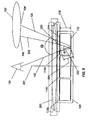
- Figure 8 is a schematic side profile view of another embodiment of the interferometric modulator display 100 that includes a converging lens 200 that spans the entire viewing surface of the display 100.
- the lens 200 is positioned at a distance along the optical axis 201 from the modulators 110 that is less than the focal length of the lens 200.
- one optical path includes a path segment 202 along which light travels from the location 106 to the display 100.
- the lens 200 has an optical aperture that is greater than the total aperture of two or more of the interferometric modulators of the display 100.
- the lens 200 has an optical aperture that is greater than the total aperture of the array of interferometric modulators.
- At least a portion of the light from the path segment 202 is transmitted through the lens 200 and reflected via surfaces of the mirrors of the interferometric modulator 110a.
- the reflected light is again transmitted through the lens 200 to the viewer 130.
- the lens 200 selects incoming light from a location 106 on the source 102 for transmission through the modulator element 110a to the viewer 130.
- the optical paths of light to the viewer through the lens 200 are thus selected to have a greater angle of incidence with the reflective surfaces of the modulators (closer to 90°) than the angle of incidence of the optical paths to the viewer in an embodiment without the lens 200. Transmission of this light to the viewer 130 reduces the perceived color shift by altering the path length difference within the optical cavity so that the distance traveled is closer to that followed by light traveling along the optical axis 201.
- the lens 200 is configured to direct light to the viewer 130 substantially via an optical path that includes optical path segments 202,220, 222, and 122.
- the source for light traveling along path 202 is location 106 on the source 102.
- the selected location 106 is closer to the central axis of the display system than is location 104 where the light traveling along path 120 originated.
- the narrowing of the illumination source angles is substantially responsible for the steeper angles of the light rays within the modulator elements 110.
- the reflected path segment 222 and the incident path segment220 define an angle ⁇ '.
- the lens 200 is selected so that the angle ⁇ ' is smaller than the angle ⁇ defined by the path segments 120 and 122, which correspond to light paths existing in embodiments without the lens 200, as in the display of Figure 7.
- the smaller subtended angle ⁇ ' at the interferometric modulator element 110a corresponds to a path length difference of twice the distance 224, and since ⁇ ' is smaller than ⁇ the path length 224 will be longer than the path length 118 of Figure 7.
- the longer path length corresponds to a reduction in the perceived color shift of off-axis light reflected by the display 100.
- the display 100 is a direct-view interferometric display that is viewed using the light source 102 having a broadband, ambient illumination in which substantially all points in the field behind the viewer are similarly illuminated so that light arriving from one source location is on average insignificantly different than light arriving from any other source location.
- the lens 200 thus selects light from a point in the field that subtends a smaller angle with respect to the viewer 130 than would be selected without the lens 200.
- the converging lens 200 is a convex lens.
- One of skill in the art can use techniques that are well known in the art to derive the shape and materials for constructing the lens 200 to have the desired characteristic properties.
- the lens 200 is typically undesirably large and bulky.
- structural support (not shown) for the lens 200 can add cost and complexity to the display 100, and thus tends to render impractical the integration of lens 200 into such a typical product.
- embodiments may include any other suitable converging optical element, including a Fresnel lens.
- the Fresnel lens is desirably smaller and less bulky than a simple curved lens embodiment such as that shown as the lens 200 in Figure 8.
- a simple curved lens embodiment such as that shown as the lens 200 in Figure 8.
- Other embodiments of the lens 200 may include any other type of converging lens or optical element that is known in the art.
- Diffractive optical elements which may be considered conceptually to be step-wise approximations to an optical function (for example a Fresnel lens), are light modulating elements that in one embodiment comprise structures that have been patterned and etched onto a substrate using photolithographic techniques so as to diffract light in a predetermined manner, for example, to converge or focus light.
- the dimensions of the structures are a few microns in size, depending on the wavelength of the light to be affected.
- a suitable computer program is typically used to calculate the pattern and shape of the structures that define a DOE to perform a particular optical function, e.g., of a converging lens.
- a particular optical function e.g., of a converging lens.
- Examples of such software include CODE V, available from Optical Research Associates, Inc., Pasadena, CA, OSLO, available from Lambda Research Associates, Inc, Rochester, NY, and ZEMAX, available from Focus Software, Arlington, AZ.
- diffractive optics including the calculation of a suitable lens structure, may be found in Diffractive Optics: Design, Fabrication, & Test, Donald C. O'Shea, Thomas J. Sulski, Alan D. Kathman, Dennis W. Prather (Society of Photo-Optical Instrumentation Engineering 2003).
- a binary optical element is a diffractive optical element comprising a discrete number of diffractive surfaces.
- the simplest form is comprised of single step elements, having two diffractive surfaces, such as formed by single lithographic step. The two surfaces introduce either a 0 or ⁇ -phase difference in the incident wavefront.
- a multilevel binary element includes N levels of material, e.g., as formed by N lithographic steps. The N levels can produce 2 N phase levels.
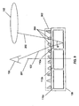
- Figure 9 is a schematic side profile view of an embodiment of the interferometric modulator display 100 that includes a diffractive optical element 302 in the optical path from the location 106 of the light source 102 to the viewer 130 via the interferometric modulator element 110a.
- the DOE 302 includes a converging DOE.
- a converging DOE is a DOE that is configured to perform the optical function of a converging lens, i.e., converge light toward the optical axis 201 of the DOE 302. It is to be recognized that the elements depicted in each of Figures 7-10 are not drawn to scale nor intended to be accurate illustrations of any structure for performing the optical functions attributed to the elements.
- the diffractive optical element (DOE) 302 typically includes a large number of small elements 304. Each of the elements 304 includes a stack of one or more elements. Some such elements 304 may define a staircase-like shape. As discussed above, the size and position of the elements 304 are typically calculated using a computer and suitable software.
- the elements are arranged in a pattern that defines a set of concentric circular rings.
- the elements 302 are grouped into local structures that collectively accomplish the optical functions described herein.
- the elements 304 can be formed using photolithographic techniques using suitable materials such as photoresist, hardened photo resist (e.g., hard baked in an oven), silica, fused silica, or plastics.
- a series of layers of material having a particular thickness and index of refraction are deposited and etched to form the elements 304 of the DOE 302.
- the DOE 302 selects light rays originating from the location 106 of the light source 102. At least a portion of this light is reflected by the interferometric modulator element 110a along the path segment 122 to the viewer 130.
- the DOE 302 is formed on a separate substrate that is attached to the display 100.
- the separate substrate includes a film.
- the display 100 may include a diffuser (not shown) for scattering the specular light reflected by the interferometric modulator elements 110a in a generally lambertian pattern.
- the diffuser includes the DOE 302.
- the DOE 302 is formed on the same substrate as the interferometric modulators 110a, 110b, and 110c of the display 100.
- the interferometric modulators 110a, 110b, and 110c may be formed on a glass substrate.
- each of the interferometric modulators 110 110a, 110b, and 110c is formed on a first side of the glass substrate and the DOE 302 is formed on the opposite side of the glass substrate.
- the DOE 302 is formed on the same side of the substrate as the modulators 110.
- the elements 304 are formed on the substrate and covered with a planarization layer.
- the interferometric modulators 110 110a, 110b, and 110c are then formed on the planarization layer.
- the planarization material has an index of refraction that is different from the index of refraction of the material used to make the diffractive elements 304.
- the pattern of the diffractive elements 304 in the DOE 302 is calculated based on the indices of refraction of both the material forming the diffractive elements 304 and the material forming the planarization layer.
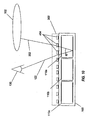
- the embodiment of the DOE 302 in Figure 10 is created by use of a set of BOE structures 404 that generally are formed to have approximately the same height or thickness as each other.
- the exemplary DOE 302 of Figure 10 is depicted as having uniformly spaced structures 404, the width and the spacing of the structures 404 may be adjusted to achieve the desired optical function.
- the DOE 302 may be formed from a single layer of material that is photolithographically patterned and etched. Such an embodiment of the DOE 302 is formed in fewer steps than the embodiment of the multi-level binary optical element 302 of Figure 9.
- the single level DOE 302 may be placed in different positions and on different substrates and planarized in the same ways as described above for the multiple level DOE 302.
- Binary optical elements such as DOE 302 define only an approximation of a desired optical function. Generally, the more layers in the binary optical element, the better the approximation of the desired optical function. However, an approximation of the optical functions of the converging lens 200 at least partially reduces the color shift of the light from the light source 102 that is reflected by the interferometric modulator 110a to the viewer 130. In some embodiments, this partial reduction in color shift is sufficient to improve the perceived color accuracy of the display 100 for off-axis light sources and off-axis viewing.
- Embodiments of the DOE 302 may be formed in relation to the display 100 as with any of the embodiments described above with respect to the DOE 302.
- the DOE 302 may be formed on a diffuser, on a separate substrate, or on either side of the substrate of the interferometric modulators 110a, 110b, and 110c.
- optical element such as the diffractive optical element 302
- the optical element may be configured to reduce this color shift for at least a portion of the display.
- Embodiments of the diffractive optical element 302 may be configured to perform other optical functions. For example, it may be desirable in some embodiments to direct light from the display into a range of preferred viewing positions. Thus, in such embodiments, the diffractive optical element 302 may also be configured to direct light from the display 100 so as to control the field of view, to limit or expand the direction of view of the image, or to control the size of the image.
- the optical element includes a lenticular component that is configured to control the field of view of the display horizontally (with reference to a viewer) by directing a portion of the light from the display to a range of angles, e.g., by spreading the light from the display 100 around the horizontal axis of the display 100.
- the optical element spreads the light through a greater range of angles along the horizontal axis than along the vertical axis. This increase the amount of light received at off axis viewing positions, for example, at a range of seating positions in a room around the display.
- the diffractive optical element 302 is further configured to perform the optical function of a lenticular lens.
- the display 100 may include or be configured to use a particular light source or set of light sources having known positions relative to the display 100.
- the diffractive optical element 302 is tailored to direct the light based on the location, amount of illumination, or aperture of the light sources.
- the light sources include one or more light emitting diodes positioned around the front of the display 100 so as to illuminate the display.
- the DOE 302 is configured to compensate for non-uniform illumination of the display by the light sources or for the effects of other undesirable properties of the light sources by, for example, varying the amount of light transmitted through the DOE 302 over the surface of the display 100.
- FIGS 11A and 11B are system block diagrams illustrating an embodiment of a display device 2040.
- the display device 2040 can be, for example, a cellular or mobile telephone.
- the same components of display device 2040 or slight variations thereof are also illustrative of various types of display devices such as televisions and portable media players.
- the display device 2040 includes a housing 2041, a display 2030, an antenna 2043, a speaker 2045, an input device 2048, and a microphone 2046.
- the housing 2041 is generally formed from any of a variety of manufacturing processes as are well known to those of skill in the art, including injection molding, and vacuum forming.
- the housing 2041 may be made from any of a variety of materials, including but not limited to plastic, metal, glass, rubber, and ceramic, or a combination thereof.
- the housing 2041 includes removable portions (not shown) that may be interchanged with other removable portions of different color, or containing different logos, pictures, or symbols.
- the display 2030 of exemplary display device 2040 may be any of a variety of displays, including a bi-stable display, as described herein.
- the display 2030 includes a flat-panel display, such as plasma, EL, OLED, STN LCD, or TFT LCD as described above, or a non-flat-panel display, such as a CRT or other tube device, as is well known to those of skill in the art.
- the display 2030 includes an interferometric modulator display, as described herein.
- the components of one embodiment of exemplary display device 2040 are schematically illustrated in Figure 11B.
- the illustrated exemplary display device 2040 includes a housing 2041 and can include additional components at least partially enclosed therein.
- the exemplary display device 2040 includes a network interface 2027 that includes an antenna 2043 which is coupled to a transceiver 2047.
- the transceiver 2047 is connected to the processor 2021, which is connected to conditioning hardware 2052.
- the conditioning hardware 2052 may be configured to condition a signal (e.g. filter a signal).
- the conditioning hardware 2052 is connected to a speaker 2045 and a microphone 2046.
- the processor 2021 is also connected to an input device 2048 and a driver controller 2029.
- the driver controller 2029 is coupled to a frame buffer 2028 and to the array driver 2022, which in turn is coupled to a display array 2030.
- a power supply 2050 provides power to all components as required by the particular exemplary display device 2040 design.
- the network interface 2027 includes the antenna 2043 and the transceiver 2047 so that the exemplary display device 2040 can communicate with one or more devices over a network. In one embodiment the network interface 2027 may also have some processing capabilities to relieve requirements of the processor 2021.
- the antenna 2043 is any antenna known to those of skill in the art for transmitting and receiving signals. In one embodiment, the antenna transmits and receives RF signals according to the IEEE 802.11 standard, including IEEE 802.11(a), (b), or (g). In another embodiment, the antenna transmits and receives RF signals according to the BLUETOOTH standard. In the case of a cellular telephone, the antenna is designed to receive CDMA, GSM, AMPS or other known signals that are used to communicate within a wireless cell phone network.
- the transceiver 2047 pre-processes the signals received from the antenna 2043 so that they may be received by and further manipulated by the processor 2021.
- the transceiver 2047 also processes signals received from the processor 2021 so that they may be transmitted from the exemplary display device 2040 via the antenna 2043.
- the transceiver 2047 can be replaced by a receiver.
- network interface 2027 can be replaced by an image source, which can store or generate image data to be sent to the processor 2021.
- the image source can be a digital video disc (DVD) or a hard-disc drive that contains image data, or a software module that generates image data.
- Processor 2021 generally controls the overall operation of the exemplary display device 2040.
- the processor 2021 receives data, such as compressed image data from the network interface 2027 or an image source, and processes the data into raw image data or into a format that is readily processed into raw image data.
- the processor 2021 then sends the processed data to the driver controller 2029 or to frame buffer 2028 for storage.
- Raw data typically refers to the information that identifies the image characteristics at each location within an image. For example, such image characteristics can include color, saturation, and gray-scale level.
- the processor 2021 includes a microcontroller, CPU, or logic unit to control operation of the exemplary display device 2040.
- Conditioning hardware 2052 generally includes amplifiers and filters for transmitting signals to the speaker 2045, and for receiving signals from the microphone 2046.
- Conditioning hardware 2052 may be discrete components within the exemplary display device 2040, or may be incorporated within the processor 2021 or other components.
- the driver controller 2029 takes the raw image data generated by the processor 2021 either directly from the processor 2021 or from the frame buffer 2028 and reformats the raw image data appropriately for high speed transmission to the array driver 2022. Specifically, the driver controller 2029 reformats the raw image data into a data flow having a raster-like format, such that it has a time order suitable for scanning across the display array 2030. Then the driver controller 2029 sends the formatted information to the array driver 2022.
- a driver controller 2029 such as a LCD controller, is often associated with the system processor 2021 as a stand-alone Integrated Circuit (IC), such controllers may be implemented in many ways. They may be embedded in the processor 2021 as hardware, embedded in the processor 2021 as software, or fully integrated in hardware with the array driver 2022.
- IC Integrated Circuit
- the array driver 2022 receives the formatted information from the driver controller 2029 and reformats the video data into a parallel set of waveforms that are applied many times per second to the hundreds and sometimes thousands of leads coming from the display's x-y matrix of pixels.
- driver controller 2029, array driver 2022, and display array 2030 are appropriate for any of the types of displays described herein.
- driver controller 2029 is a conventional display controller or a bi-stable display controller (e.g., an interferometric modulator controller).
- array driver 2022 is a conventional driver or a bi-stable display driver (e.g., an interferometric modulator display).
- a driver controller 2029 is integrated with the array driver 2022.
- display array 2030 is a typical display array or a bi-stable display array (e.g., a display including an array of interferometric modulators).
- the input device 2048 allows a user to control the operation of the exemplary display device 2040.
- input device 2048 includes a keypad, such as a QWERTY keyboard or a telephone keypad, a button, a switch, a touch-sensitive screen, a pressure- or heat-sensitive membrane.
- the microphone 2046 is an input device for the exemplary display device 2040. When the microphone 2046 is used to input data to the device, voice commands may be provided by a user for controlling operations of the exemplary display device 2040.
- Power supply 2050 can include a variety of energy storage devices as are well known in the art.
- power supply 2050 is a rechargeable battery, such as a nickel-cadmium battery or a lithium ion battery.
- power supply 2050 is a renewable energy source, a capacitor, or a solar cell, including a plastic solar cell, and solar-cell paint.
- power supply 2050 is configured to receive power from a wall outlet.
- control programmability resides, as described above, in a driver controller which can be located in several places in the electronic display system. In some cases control programmability resides in the array driver 2022. Those of skill in the art will recognize that the above-described optimization may be implemented in any number of hardware and/or software components and in various configurations.
- embodiments of the invention overcome many of the problems in the art by providing a interferometric modulator display with an optical element that reduces the color shift evident as viewingangle or light angle change. Moreover, this optical element can be cost-effectively included in the display by the use of a few additional photolithographic steps.
Abstract
Description
- The field of the invention relates to microelectromechanical systems (MEMS).
- Microelectromechanical systems (MEMS) include micro mechanical elements, actuators, and electronics. Micromechanical elements may be created using deposition, etching, and or other micromachining processes that etch away parts of substrates and/or deposited material layers or that add layers to form electrical and electromechanical devices. One type of MEMS device is called an interferometric modulator. An interferometric modulator may comprise a pair of conductive plates, one or both of which may be transparent and/or reflective in whole or part and capable of relative motion upon application of an appropriate electrical signal. One plate may comprise a stationary layer deposited on a substrate, the other plate may comprise a metallic membrane separated from the stationary layer by an air gap. Such devices have a wide range of applications, and it would be beneficial in the art to utilize and/or modify the characteristics of these types of devices so that their features can be exploited in improving existing products and creating new products that have not yet been developed.
- The system, method, and devices of the invention each have several aspects, no single one of which is solely responsible for its desirable attributes. Without limiting the scope of this invention, its more prominent features will now be discussed briefly. After considering this discussion, and particularly after reading the section entitled "Detailed Description of Certain Embodiments" one will understand how the features of this invention provide advantages over other display devices.
- One embodiment is a display system for displaying an image. The display system includes a plurality of interferometric modulators configured to modulate light incident on a surface thereof. The display system further includes a converging optical element positioned with respect to a surface of at least one of the plurality of interferometric modulators such that a focal length of the optical element is greater than a distance between the optical element and the surface.
- Another embodiment is a method of fabricating a display system. The method includes forming a plurality of interferometric modulators on a first substrate. The method further includes forming a converging optical element on a second substrate. The optical element is positioned with respect to at least one surface of at least one of the plurality of interferometric modulators such that a focal length of the optical element is greater than a distance between the optical element and the at least one surface. Another embodiment is a display system fabricated according to this method.
- Another embodiment is a display system for displaying an image. The display system includes means for interferometrically modulating light incident thereon and means for converging light adapted so as to limit color shift of at least a portion of the image between different viewing locations.
- Another embodiment is a method of fabricating a display system comprising: forming a plurality of interferometric modulators on a first substrate; and forming a converging diffractive optical element on a second substrate, the optical element positioned so as to redirect light that is incident on at least one surface of at least one of the plurality of interferometric modulators.
- Another embodiment is a display system for displaying an image, the display system comprising: means for interferometrically modulating light incident thereon; and means for diffracting light to redirect light incident on said means for interferometrically modulating light, wherein said means for diffracting light is configured to converge said light.
- Another embodiment is a display system for displaying an image, the display system comprising: a plurality of interferometric modulators configured to modulate light incident thereon; and a converging diffractive optical element configured to redirect light incident on at least one of the plurality of interferometric modulators.
- Another embodiment is a display system for displaying an image, the display system comprising: means for interferometrically modulating light incident thereon; and means for diffracting light to redirect light incident on said means for interferometrically modulating light.
-
- Figure 1 is an isometric view depicting a portion of one embodiment of an interferometric modulator display in which a movable reflective layer of a first interferometric modulator is in a released position and a movable reflective layer of a second interferometric modulator is in an actuated position.
- Figure 2 is a system block diagram illustrating one embodiment of an electronic device incorporating a 3x3 interferometric modulator display.
- Figure 3 is a diagram of movable mirror position versus applied voltage for one exemplary embodiment of an interferometric modulator of Figure 1.
- Figure 4 is an illustration of a set of row and column voltages that may be used to drive an interferometric modulator display.
- Figures 5A and 5B illustrate one exemplary timing diagram for row and column signals that may be used to write a frame of display data to the 3x3 interferometric modulator display of Figure 2.
- Figure 6A is a cross section of the device of Figure 1.
- Figure 6B is a cross section of an alternative embodiment of an interferometric modulator.
- Figure 6C is a cross section of another alternative embodiment of an interferometric modulator.
- Figure 7 is a schematic side profile view of one embodiment of an interferometric modulator display depicting the optical path from a light source to a viewer via an interferometric modulator element of the display.
- Figure 8 is a schematic side profile view of another embodiment of the interferometric modulator display, similar to that depicted in Figure 7, that includes a lens in the optical path from the light source to the viewer via the interferometric modulator element.
- Figure 9 is a schematic side profile view of another embodiment of the interferometric modulator display, similar to that depicted in Figure 8, that includes a diffractive optical element in the optical path from the light source to the viewer via the interferometric modulator element.
- Figure 10 is a schematic side profile view of another embodiment of the interferometric modulator display, similar to that depicted in Figure 8, that includes a single level binary optical element in the optical path from the light source to the viewer via the interferometric modulator element.
- Figures 11A and 11B are system block diagrams illustrating an embodiment of a visual display device comprising a plurality of interferometric modulators.
- The following detailed description is directed to certain specific embodiments of the invention. However, the invention can be embodied in a multitude of different ways. In this description, reference is made to the drawings wherein like parts are designated with like numerals throughout.
- In preferred embodiments, the invention includes an optical element, such as a lens, fresnel lens, diffractive optical element, or binary optical element, positioned between an interferometric display and a viewer of the display. The optical element is configured to reduce color shift that may be seen as the viewing angle or light angle changes.
- The following detailed description is directed to certain specific embodiments of the invention. However, the invention can be embodied in a multitude of different ways. In this description, reference is made to the drawings wherein like parts are designated with like numerals throughout. As will be apparent from the following description, the invention may be implemented in any device that is configured to display an image, whether in motion (e.g., video) or stationary (e.g., still image), and whether textual or pictorial. More particularly, it is contemplated that the invention may be implemented in or associated with a variety of electronic devices such as, but not limited to, mobile telephones, wireless devices, personal data assistants (PDAs), handheld or portable computers, GPS receivers/navigators, cameras, MP3 players, camcorders, game consoles, wrist watches, clocks, calculators, television monitors, flat panel displays, computer monitors, auto displays (e.g., odometer display, etc.), cockpit controls and/or displays, display of camera views (e.g., display of a rear view camera in a vehicle), electronic photographs, electronic billboards or signs, projectors, architectural structures, packaging, and aesthetic structures (e.g., display of images on a piece of jewelry). MEMS devices of similar structure to those described herein can also be used in non-display applications such as in electronic switching devices.
- One interferometric modulator display embodiment comprising an interferometric MEMS display element is illustrated in Figure 1. In these devices, the pixels are in either a bright or dark state. In the bright ("on" or "open") state, the display element reflects a large portion of incident visible light to a user. When in the dark ("off" or "closed") state, the display element reflects little incident visible light to the user. Depending on the embodiment, the light reflectance properties of the "on" and "off" states may be reversed. MEMS pixels can be configured to reflect predominantly at selected colors, allowing for a color display in addition to black and white.
- Figure 1 is an isometric view depicting two adjacent pixels in a series of pixels of a visual display, wherein each pixel comprises a MEMS interferometric modulator. In some embodiments, an interferometric modulator display comprises a row/column array of these interferometric modulators. Each interferometric modulator includes a pair of reflective layers positioned at a variable and controllable distance from each other to form a resonant optical cavity with at least one variable dimension. In one embodiment, one of the reflective layers may be moved between two positions. In the first position, referred to herein as the released state, the movable layer is positioned at a relatively large distance from a fixed partially reflective layer. In the second position, the movable layer is positioned more closely adjacent to the partially reflective layer. Incident light that reflects from the two layers interferes constructively or destructively depending on the position of the movable reflective layer, producing either an overall reflective or non-reflective state for each pixel.
- The depicted portion of the pixel array in Figure 1 includes two adjacent
interferometric modulators interferometric modulator 12a on the left, a movable and highly reflective layer 14a is illustrated in a released position at a predetermined distance from a fixed partially reflective layer 16a. In theinterferometric modulator 12b on the right, the movable highlyreflective layer 14b is illustrated in an actuated position adjacent to the fixed partiallyreflective layer 16b. - The
fixed layers 16a, 16b are electrically conductive, partially transparent and partially reflective, and may be fabricated, for example, by depositing one or more layers each of chromium and indium-tin-oxide onto atransparent substrate 20. The layers are patterned into parallel strips, and may form row electrodes in a display device as described further below. Themovable layers 14a, 14b may be formed as a series of parallel strips of a deposited metal layer or layers (orthogonal to therow electrodes 16a, 16b) deposited on top ofposts 18 and an intervening sacrificial material deposited between theposts 18. When the sacrificial material is etched away, the deformable metal layers are separated from the fixed metal layers by a definedair gap 19. A highly conductive and reflective material such as aluminum may be used for the deformable layers, and these strips may form column electrodes in a display device. - With no applied voltage, the
cavity 19 remains between the layers 14a, 16a and the deformable layer is in a mechanically relaxed state as illustrated by thepixel 12a in Figure1. However, when a potential difference is applied to a selected row and column, the capacitor formed at the intersection of the row and column electrodes at the corresponding pixel becomes charged, and electrostatic forces pull the electrodes together. If the voltage is high enough, the movable layer is deformed and is forced against the fixed layer (a dielectric material which is not illustrated in this Figure may be deposited on the fixed layer to prevent shorting and control the separation distance) as illustrated by thepixel 12b on the right in Figure 1. The behavior is the sameregardless of the polarity of the applied potential difference. In this way, row/column actuation that can control the reflective vs. non-reflective pixel states is analogous in many ways to that used in conventional LCD and other display technologies. - Figures 2 through 5 illustrate one exemplary process and system for using an array of interferometric modulators in a display application. Figure 2 is a system block diagram illustrating one embodiment of an electronic device that may incorporate aspects of the invention. In the exemplary embodiment, the electronic device includes a
processor 21 which may be any general purpose single- or multi-chip microprocessor such as an ARM, Pentium®, Pentium II®, Pentium III®, Pentium IV®, Pentium®Pro, an 8051, a MIPS®, a Power PC®, an ALPHA® or any special purpose microprocessor such as a digital signal processor, microcontroller, or a programmable gate array. As is conventional in the art, theprocessor 21 may be configured to execute one or more software modules. In addition to executing an operating system, the processor may be configured to execute one or more software applications, including a web browser, a telephone application, an email program, or any other software application. - In one embodiment, the
processor 21 is also configured to communicate with anarray controller 22. In one embodiment, thearray controller 22 includes arow driver circuit 24 and acolumn driver circuit 26 that provide signals to apixel array 30. The cross section of the array illustrated in Figure 1 is shown by the lines 1-1 in Figure 2. For MEMS interferometric modulators, the row/column actuation protocol may take advantage of a hysteresis property of these devices illustrated in Figure 3. It may require, for example, a 10 volt potential difference to cause a movable layer to deform from the released state to the actuated state. However, when the voltage is reduced from that value, the movable layer maintains its state as the voltage drops back below 10 volts. In the exemplary embodiment of Figure 3, the movable layer does not release completely until the voltage drops below 2 volts. There is thus a range of voltage, about 3 to 7 V in the example illustrated in Figure 3, where there exists a window of applied voltage within which the device is stable in either the released or actuated state. This is referred to herein as the "hysteresis window" or "stability window." For a display array having the hysteresis characteristics of Figure 3, the row/column actuation protocol can be designed such that during row strobing, pixels in the strobed row that are to be actuated are exposed to a voltage difference of about 10 volts, and pixels that are to be released are exposed to a voltage difference of close to zero volts. After the strobe, the pixels are exposed to a steady state voltage difference of about 5 volts such that they remain in whatever state the row strobe put them in. After being written, each pixel sees a potential difference within the "stability window" of 3-7 volts in this example. This feature makes the pixel design illustrated in Figure 1 stable under the same applied voltage conditions in either an actuated or released pre-existing state. Since each pixel of the interferometric modulator, whether in the actuated or released state, is essentially a capacitor formed by the fixed and moving reflective layers, this stable state can be held at a voltage within the hysteresis window with almost no power dissipation. Essentially no current flows into the pixel if the applied potential is fixed. - In typical applications, a display frame may be created by asserting the set of column electrodes in accordance with the desired set of actuated pixels in the first row. A row pulse is then applied to the
row 1 electrode, actuating the pixels corresponding to the asserted column lines. The asserted set of column electrodes is then changed to correspond to the desired set of actuated pixels in the second row. A pulse is then applied to therow 2 electrode, actuating the appropriate pixels inrow 2 in accordance with the asserted column electrodes. Therow 1 pixels are unaffected by therow 2 pulse, and remain in the state they were set to during therow 1 pulse. This may be repeated for the entire series of rows in a sequential fashion to produce the frame. Generally, the frames are refreshed and/or updated with new display data by continually repeating this process at some desired number of frames per second. A wide variety of protocols for driving row and column electrodes of pixel arrays to produce display frames are also well known and may be used in conjunction with the present invention. - Figures 4 and 5 illustrate one possible actuation protocol for creating a display frame on the 3x3 array of Figure 2. Figure 4 illustrates a possible set of column and row voltage levels that may be used for pixels exhibiting the hysteresis curves of Figure 3. In the Figure 4 embodiment, actuating a pixel involves setting the appropriate column to -Vbias, and the appropriate row to +ΔV, which may correspond to -5 volts and +5 volts respectively Releasing the pixel is accomplished by setting the appropriate column to +Vbias, and the appropriate row to the same +ΔV, producing a zero volt potential difference across the pixel. In those rows where the row voltage is held at zero volts, the pixels are stable in whatever state they were originally in, regardless of whether the column is at +Vbias or -Vbias.
- Figure 5B is a timing diagram showing a series of row and column signals applied to the 3x3 array of Figure 2 which will result in the display arrangement illustrated in Figure 5A, where actuated pixels are non-reflective. Prior to writing the frame illustrated in Figure 5A, the pixels can be in any state, and in this example, all the rows are at 0 volts, and all the columns are at +5 volts. With these applied voltages, all pixels are stable in their existing actuated or released states.
- In the Figure 5A frame, pixels (1,1), (1,2), (2,2), (3,2) and (3,3) are actuated. To accomplish this, during a "line time" for
row 1,columns column 3 is set to +5 volts. This does not change the state of any pixels, because all the pixels remain in the 3-7 volt stability window.Row 1 is then strobed with a pulse that goes from 0, up to 5 volts, and back to zero. This actuates the (1,1) and (1,2) pixels and releases the (1,3) pixel. No other pixels in the array are affected. To setrow 2 as desired,column 2 is set to -5 volts, andcolumns Row 3 is similarly set by settingcolumns column 1 to +5 volts. Therow 3 strobe sets therow 3 pixels as shown in Figure 5A. After writing the frame, the row potentials are zero, and the column potentials can remain at either +5 or-5 volts, and the display is then stable in the arrangement of Figure 5A. It will be appreciated that the same procedure can be employed for arrays of dozens or hundreds of rows and columns. It will also be appreciated that the timing, sequence, and levels of voltages used to perform row and column actuation can be varied widely within the general principles outlined above, and the above example is exemplary only, and any actuation voltage method can be used with the present invention. - The details of the structure of interferometric modulators that operate in accordance with the principles set forth above may vary widely. For example, Figures 6A-6C illustrate three different embodiments of the moving mirror structure. Figure 6A is a cross section of the embodiment of Figure 1, where a strip of
metal material 14 is deposited on orthogonally extending supports 18. In Figure 68, the moveablereflective material 14 is attached to supports at the corners only, ontethers 32. In Figure 6C, the moveablereflective material 14 is suspended from adeformable layer 34. This embodiment has benefits because the structural design and materials used for thereflective material 14 can be optimized with respect to the optical properties, and the structural design and materials used for thedeformable layer 34 can be optimized with respect to desired mechanical properties. The production of various types of interferometric devices is described in a variety of published documents, including, for example, U.S. Published Application 2004/0051929. A wide variety of well known techniques may be used to produce the above described structures involving a series of material deposition, patterning, and etching steps. - Figure 7 is a schematic side profile view of one embodiment of an
interferometric modulator display 100 depicting an optical path from alight source 102 to aviewer 130 via thedisplay 100. Thelight source 102 depicted in Figure 7 transmits light from a range of locations that include, for example,locations interferometric modulator display 100 includes an array of the interferometriclight modulators display 100 may include thousands or millions of modulators. Each of thelight modulators mirrors mirrors distance 116 so as to define an optical cavity therebetween. The color of light that is reflected from the optical cavity is at least partly determined by thedistance 116. In an exemplary embodiment of thedisplay 100 that is configured to produce a color image, thedistance 116 is selected for each of thelight modulators light modulator display 100. - In one embodiment, the
display 100 produces a displayed image by reflecting light that arrives at thedisplay 100 along many optical paths from many sources. In one exemplary optical path, the light fromlocation 104 arrives at thedisplay 100 along thepath 120. This light is modulated by theinterferometric modulator element 110a so that a portion of the light alongpath 120 is reflected along apath 122 to theviewer 130. The incident and reflected light alongpaths source 102 to theviewer 130 that is reflected frommirror 114 travels a shorter path (not shown) than does light traveling from thesource 102 to theviewer 130 that is reflected frommirror 112. The path length difference between these two paths, along with several other factors, determines the peak wavelength of light that theviewer 130 perceives as being reflected from themodulator element 110a. This path length difference is roughly proportional to the cosine of the angleθ/2 multiplied times thedistance 116. For θ=0, cos θ/2=1, and the path length difference is twice thedistance 116. As the angle θ becomes larger cos θ/2 decreases, and the path length distance (twice the distance 118) defined by the twomirrors light following paths distance 116. This decreasedoptical path distance 118 generated in themodulator element 110a corresponds to a shift in the color of light that is reflected by themodulator elements 110a. At sufficiently large angles θ, theviewer 130 can perceive this color shift in the colors produced by thedisplay 120. - Figure 8 is a schematic side profile view of another embodiment of the
interferometric modulator display 100 that includes a converginglens 200 that spans the entire viewing surface of thedisplay 100. Thelens 200 is positioned at a distance along theoptical axis 201 from the modulators 110 that is less than the focal length of thelens 200. In the embodiment of Figure 8, which includes thelens 200, one optical path includes apath segment 202 along which light travels from thelocation 106 to thedisplay 100. In one embodiment, thelens 200 has an optical aperture that is greater than the total aperture of two or more of the interferometric modulators of thedisplay 100. In one embodiment, thelens 200 has an optical aperture that is greater than the total aperture of the array of interferometric modulators. At least a portion of the light from thepath segment 202 is transmitted through thelens 200 and reflected via surfaces of the mirrors of theinterferometric modulator 110a. The reflected light is again transmitted through thelens 200 to theviewer 130. Conceptually, thelens 200 selects incoming light from alocation 106 on thesource 102 for transmission through themodulator element 110a to theviewer 130. The optical paths of light to the viewer through thelens 200 are thus selected to have a greater angle of incidence with the reflective surfaces of the modulators (closer to 90°) than the angle of incidence of the optical paths to the viewer in an embodiment without thelens 200. Transmission of this light to theviewer 130 reduces the perceived color shift by altering the path length difference within the optical cavity so that the distance traveled is closer to that followed by light traveling along theoptical axis 201. - In one embodiment, the
lens 200 is configured to direct light to theviewer 130 substantially via an optical path that includes optical path segments 202,220, 222, and 122. The source for light traveling alongpath 202 islocation 106 on thesource 102. The selectedlocation 106 is closer to the central axis of the display system than islocation 104 where the light traveling alongpath 120 originated. In such an embodiment of thedisplay 100, the narrowing of the illumination source angles is substantially responsible for the steeper angles of the light rays within the modulator elements 110. The reflectedpath segment 222 and the incident path segment220 define an angle θ'. Thelens 200 is selected so that the angle θ' is smaller than the angle θ defined by thepath segments lens 200, as in the display of Figure 7. The smaller subtended angle θ' at theinterferometric modulator element 110a corresponds to a path length difference of twice thedistance 224, and since θ' is smaller than θ thepath length 224 will be longer than thepath length 118 of Figure 7. The longer path length corresponds to a reduction in the perceived color shift of off-axis light reflected by thedisplay 100. - In one embodiment, the
display 100 is a direct-view interferometric display that is viewed using thelight source 102 having a broadband, ambient illumination in which substantially all points in the field behind the viewer are similarly illuminated so that light arriving from one source location is on average insignificantly different than light arriving from any other source location. Thelens 200 thus selects light from a point in the field that subtends a smaller angle with respect to theviewer 130 than would be selected without thelens 200. - In one embodiment, the converging
lens 200 is a convex lens. One of skill in the art can use techniques that are well known in the art to derive the shape and materials for constructing thelens 200 to have the desired characteristic properties. However, in many typical display applications, such as in handheld or other portable display devices, thelens 200 is typically undesirably large and bulky. Moreover, structural support (not shown) for thelens 200 can add cost and complexity to thedisplay 100, and thus tends to render impractical the integration oflens 200 into such a typical product. - As an alternative to the converging
lens 200, for example, in order to reduce this bulk, embodiments may include any other suitable converging optical element, including a Fresnel lens. The Fresnel lens is desirably smaller and less bulky than a simple curved lens embodiment such as that shown as thelens 200 in Figure 8. However, even the reduced bulk of the Fresnel lens still tends to be impractically large for many portable applications. Other embodiments of thelens 200 may include any other type of converging lens or optical element that is known in the art. - An alternative to use of a lens in light control applications is use of diffractive optical elements including holographic optical elements. Diffractive optical elements ("DOE"), which may be considered conceptually to be step-wise approximations to an optical function (for example a Fresnel lens), are light modulating elements that in one embodiment comprise structures that have been patterned and etched onto a substrate using photolithographic techniques so as to diffract light in a predetermined manner, for example, to converge or focus light. In one embodiment, the dimensions of the structures are a few microns in size, depending on the wavelength of the light to be affected. A suitable computer program is typically used to calculate the pattern and shape of the structures that define a DOE to perform a particular optical function, e.g., of a converging lens. Examples of such software include CODE V, available from Optical Research Associates, Inc., Pasadena, CA, OSLO, available from Lambda Research Associates, Inc, Rochester, NY, and ZEMAX, available from Focus Software, Tucson, AZ. For example, more details regarding diffractive optics, including the calculation of a suitable lens structure, may be found in Diffractive Optics: Design, Fabrication, & Test, Donald C. O'Shea, Thomas J. Sulski, Alan D. Kathman, Dennis W. Prather (Society of Photo-Optical Instrumentation Engineering 2003).
- One type of DOE is a binary optical element ("BOE"). A binary optical element is a diffractive optical element comprising a discrete number of diffractive surfaces. The simplest form is comprised of single step elements, having two diffractive surfaces, such as formed by single lithographic step. The two surfaces introduce either a 0 or π-phase difference in the incident wavefront. A multilevel binary element includes N levels of material, e.g., as formed by N lithographic steps. The N levels can produce 2N phase levels.
- Figure 9 is a schematic side profile view of an embodiment of the
interferometric modulator display 100 that includes a diffractiveoptical element 302 in the optical path from thelocation 106 of thelight source 102 to theviewer 130 via theinterferometric modulator element 110a. The illustrated embodiment of theDOE 302 is a binary optical element having N=3. In other embodiments, N may be any number. In some embodiments, N may be 1,2,3,4, or 5. In other embodiments, N may be in the range of 1-10. - The
DOE 302 includes a converging DOE. A converging DOE is a DOE that is configured to perform the optical function of a converging lens, i.e., converge light toward theoptical axis 201 of theDOE 302. It is to be recognized that the elements depicted in each of Figures 7-10 are not drawn to scale nor intended to be accurate illustrations of any structure for performing the optical functions attributed to the elements. The diffractive optical element (DOE) 302 typically includes a large number ofsmall elements 304. Each of theelements 304 includes a stack of one or more elements. Somesuch elements 304 may define a staircase-like shape. As discussed above, the size and position of theelements 304 are typically calculated using a computer and suitable software. In one embodiment, the elements are arranged in a pattern that defines a set of concentric circular rings. In another embodiment, theelements 302 are grouped into local structures that collectively accomplish the optical functions described herein. Theelements 304 can be formed using photolithographic techniques using suitable materials such as photoresist, hardened photo resist (e.g., hard baked in an oven), silica, fused silica, or plastics. In one embodiment, a series of layers of material having a particular thickness and index of refraction are deposited and etched to form theelements 304 of theDOE 302. Thus, as with thelens 200, theDOE 302 selects light rays originating from thelocation 106 of thelight source 102. At least a portion of this light is reflected by theinterferometric modulator element 110a along thepath segment 122 to theviewer 130. - In one embodiment, the
DOE 302 is formed on a separate substrate that is attached to thedisplay 100. In one embodiment, the separate substrate includes a film. Thedisplay 100 may include a diffuser (not shown) for scattering the specular light reflected by theinterferometric modulator elements 110a in a generally lambertian pattern. In one embodiment, the diffuser includes theDOE 302. In another embodiment, theDOE 302 is formed on the same substrate as theinterferometric modulators display 100. For example, theinterferometric modulators DOE 302 is formed on the opposite side of the glass substrate. - In another embodiment, the
DOE 302 is formed on the same side of the substrate as the modulators 110. In one such embodiment, theelements 304 are formed on the substrate and covered with a planarization layer. The interferometric modulators 110 110a, 110b, and 110c are then formed on the planarization layer. In one embodiment, the planarization material has an index of refraction that is different from the index of refraction of the material used to make thediffractive elements 304. The pattern of thediffractive elements 304 in theDOE 302 is calculated based on the indices of refraction of both the material forming thediffractive elements 304 and the material forming the planarization layer. - In one embodiment, the diffractive
optical element 302 is formed of a simple, N=1, binary optical element. Figure 10 is a schematic side profile view of another embodiment of theinterferometric modulator display 100 that includes an embodiment of theDOE 302 having N=1 in the optical path from thelocation 106 of thelight source 102 to theviewer 130 via theinterferometric modulator element 110a. The embodiment of theDOE 302 in Figure 10 is created by use of a set ofBOE structures 404 that generally are formed to have approximately the same height or thickness as each other. Although theexemplary DOE 302 of Figure 10 is depicted as having uniformly spacedstructures 404, the width and the spacing of thestructures 404 may be adjusted to achieve the desired optical function. In the illustrated embodiment, theDOE 302 may be formed from a single layer of material that is photolithographically patterned and etched. Such an embodiment of theDOE 302 is formed in fewer steps than the embodiment of the multi-level binaryoptical element 302 of Figure 9. Thesingle level DOE 302 may be placed in different positions and on different substrates and planarized in the same ways as described above for themultiple level DOE 302. - Binary optical elements such as
DOE 302 define only an approximation of a desired optical function. Generally, the more layers in the binary optical element, the better the approximation of the desired optical function. However, an approximation of the optical functions of the converginglens 200 at least partially reduces the color shift of the light from thelight source 102 that is reflected by theinterferometric modulator 110a to theviewer 130. In some embodiments, this partial reduction in color shift is sufficient to improve the perceived color accuracy of thedisplay 100 for off-axis light sources and off-axis viewing. - Embodiments of the
DOE 302 may be formed in relation to thedisplay 100 as with any of the embodiments described above with respect to theDOE 302. For example, theDOE 302 may be formed on a diffuser, on a separate substrate, or on either side of the substrate of the interferometric modulators 110a, 110b, and 110c. - For larger displays, e.g., displays with diagonal sizes of greater than approximately 30 inches, at typical household viewing distances, e.g., a few meters, a viewer may perceive angular color shift of a portion of the display even when positioned at the center of the display. It is to be recognized that embodiments of the optical element, such as the diffractive
optical element 302, may be configured to reduce this color shift for at least a portion of the display. - Embodiments of the diffractive
optical element 302 may be configured to perform other optical functions. For example, it may be desirable in some embodiments to direct light from the display into a range of preferred viewing positions. Thus, in such embodiments, the diffractiveoptical element 302 may also be configured to direct light from thedisplay 100 so as to control the field of view, to limit or expand the direction of view of the image, or to control the size of the image. In one embodiment, the optical element includes a lenticular component that is configured to control the field of view of the display horizontally (with reference to a viewer) by directing a portion of the light from the display to a range of angles, e.g., by spreading the light from thedisplay 100 around the horizontal axis of thedisplay 100. In one embodiment, the optical element spreads the light through a greater range of angles along the horizontal axis than along the vertical axis. This increase the amount of light received at off axis viewing positions, for example, at a range of seating positions in a room around the display. In one embodiment, the diffractiveoptical element 302 is further configured to perform the optical function of a lenticular lens. - In another embodiment, the
display 100 may include or be configured to use a particular light source or set of light sources having known positions relative to thedisplay 100. In such an embodiment, the diffractiveoptical element 302 is tailored to direct the light based on the location, amount of illumination, or aperture of the light sources. In one embodiment, the light sources include one or more light emitting diodes positioned around the front of thedisplay 100 so as to illuminate the display. In such an embodiment, theDOE 302 is configured to compensate for non-uniform illumination of the display by the light sources or for the effects of other undesirable properties of the light sources by, for example, varying the amount of light transmitted through theDOE 302 over the surface of thedisplay 100. - Figures 11A and 11B are system block diagrams illustrating an embodiment of a
display device 2040. Thedisplay device 2040 can be, for example, a cellular or mobile telephone. However, the same components ofdisplay device 2040 or slight variations thereof are also illustrative of various types of display devices such as televisions and portable media players. - The
display device 2040 includes ahousing 2041, adisplay 2030, anantenna 2043, aspeaker 2045, aninput device 2048, and amicrophone 2046. Thehousing 2041 is generally formed from any of a variety of manufacturing processes as are well known to those of skill in the art, including injection molding, and vacuum forming. In addition, thehousing 2041 may be made from any of a variety of materials, including but not limited to plastic, metal, glass, rubber, and ceramic, or a combination thereof. In one embodiment thehousing 2041 includes removable portions (not shown) that may be interchanged with other removable portions of different color, or containing different logos, pictures, or symbols. - The
display 2030 ofexemplary display device 2040 may be any of a variety of displays, including a bi-stable display, as described herein. In other embodiments, the display 2030includes a flat-panel display, such as plasma, EL, OLED, STN LCD, or TFT LCD as described above, or a non-flat-panel display, such as a CRT or other tube device, as is well known to those of skill in the art. However, for purposes of describing the present embodiment, thedisplay 2030 includes an interferometric modulator display, as described herein. - The components of one embodiment of
exemplary display device 2040 are schematically illustrated in Figure 11B. The illustratedexemplary display device 2040 includes ahousing 2041 and can include additional components at least partially enclosed therein. For example, in one embodiment, theexemplary display device 2040 includes anetwork interface 2027 that includes anantenna 2043 which is coupled to atransceiver 2047. Thetransceiver 2047 is connected to theprocessor 2021, which is connected toconditioning hardware 2052. Theconditioning hardware 2052 may be configured to condition a signal (e.g. filter a signal). Theconditioning hardware 2052 is connected to aspeaker 2045 and amicrophone 2046. Theprocessor 2021 is also connected to aninput device 2048 and adriver controller 2029. Thedriver controller 2029 is coupled to aframe buffer 2028 and to thearray driver 2022, which in turn is coupled to adisplay array 2030. Apower supply 2050 provides power to all components as required by the particularexemplary display device 2040 design. - The
network interface 2027 includes theantenna 2043 and thetransceiver 2047 so that theexemplary display device 2040 can communicate with one or more devices over a network. In one embodiment thenetwork interface 2027 may also have some processing capabilities to relieve requirements of theprocessor 2021. Theantenna 2043 is any antenna known to those of skill in the art for transmitting and receiving signals. In one embodiment, the antenna transmits and receives RF signals according to the IEEE 802.11 standard, including IEEE 802.11(a), (b), or (g). In another embodiment, the antenna transmits and receives RF signals according to the BLUETOOTH standard. In the case of a cellular telephone, the antenna is designed to receive CDMA, GSM, AMPS or other known signals that are used to communicate within a wireless cell phone network. Thetransceiver 2047 pre-processes the signals received from theantenna 2043 so that they may be received by and further manipulated by theprocessor 2021. Thetransceiver 2047 also processes signals received from theprocessor 2021 so that they may be transmitted from theexemplary display device 2040 via theantenna 2043. - In an alternative embodiment, the
transceiver 2047 can be replaced by a receiver. In yet another alternative embodiment,network interface 2027 can be replaced by an image source, which can store or generate image data to be sent to theprocessor 2021. For example, the image source can be a digital video disc (DVD) or a hard-disc drive that contains image data, or a software module that generates image data. -
Processor 2021 generally controls the overall operation of theexemplary display device 2040. Theprocessor 2021 receives data, such as compressed image data from thenetwork interface 2027 or an image source, and processes the data into raw image data or into a format that is readily processed into raw image data. Theprocessor 2021 then sends the processed data to thedriver controller 2029 or to framebuffer 2028 for storage. Raw data typically refers to the information that identifies the image characteristics at each location within an image. For example, such image characteristics can include color, saturation, and gray-scale level. - In one embodiment, the
processor 2021 includes a microcontroller, CPU, or logic unit to control operation of theexemplary display device 2040.Conditioning hardware 2052 generally includes amplifiers and filters for transmitting signals to thespeaker 2045, and for receiving signals from themicrophone 2046.Conditioning hardware 2052 may be discrete components within theexemplary display device 2040, or may be incorporated within theprocessor 2021 or other components. - The
driver controller 2029 takes the raw image data generated by theprocessor 2021 either directly from theprocessor 2021 or from theframe buffer 2028 and reformats the raw image data appropriately for high speed transmission to thearray driver 2022. Specifically, thedriver controller 2029 reformats the raw image data into a data flow having a raster-like format, such that it has a time order suitable for scanning across thedisplay array 2030. Then thedriver controller 2029 sends the formatted information to thearray driver 2022. Although adriver controller 2029, such as a LCD controller, is often associated with thesystem processor 2021 as a stand-alone Integrated Circuit (IC), such controllers may be implemented in many ways. They may be embedded in theprocessor 2021 as hardware, embedded in theprocessor 2021 as software, or fully integrated in hardware with thearray driver 2022. - Typically, the
array driver 2022 receives the formatted information from thedriver controller 2029 and reformats the video data into a parallel set of waveforms that are applied many times per second to the hundreds and sometimes thousands of leads coming from the display's x-y matrix of pixels. - In one embodiment, the
driver controller 2029,array driver 2022, anddisplay array 2030 are appropriate for any of the types of displays described herein. For example, in one embodiment,driver controller 2029 is a conventional display controller or a bi-stable display controller (e.g., an interferometric modulator controller). In another embodiment,array driver 2022 is a conventional driver or a bi-stable display driver (e.g., an interferometric modulator display). In one embodiment, adriver controller 2029 is integrated with thearray driver 2022. Such an embodiment is common in highly integrated systems such as cellular phones, watches, and other small area displays. In yet another embodiment,display array 2030 is a typical display array or a bi-stable display array (e.g., a display including an array of interferometric modulators). - The
input device 2048 allows a user to control the operation of theexemplary display device 2040. In one embodiment,input device 2048 includes a keypad, such as a QWERTY keyboard or a telephone keypad, a button, a switch, a touch-sensitive screen, a pressure- or heat-sensitive membrane. In one embodiment, themicrophone 2046 is an input device for theexemplary display device 2040. When themicrophone 2046 is used to input data to the device, voice commands may be provided by a user for controlling operations of theexemplary display device 2040. -
Power supply 2050 can include a variety of energy storage devices as are well known in the art. For example, in one embodiment,power supply 2050 is a rechargeable battery, such as a nickel-cadmium battery or a lithium ion battery. In another embodiment,power supply 2050 is a renewable energy source, a capacitor, or a solar cell, including a plastic solar cell, and solar-cell paint. In another embodiment,power supply 2050 is configured to receive power from a wall outlet. - In some implementations control programmability resides, as described above, in a driver controller which can be located in several places in the electronic display system. In some cases control programmability resides in the
array driver 2022. Those of skill in the art will recognize that the above-described optimization may be implemented in any number of hardware and/or software components and in various configurations. - In view of the above, one will appreciate that embodiments of the invention overcome many of the problems in the art by providing a interferometric modulator display with an optical element that reduces the color shift evident as viewingangle or light angle change. Moreover, this optical element can be cost-effectively included in the display by the use of a few additional photolithographic steps.
- While the above detailed description has shown, described, and pointed out novel features of the invention as applied to various embodiments, it will be understood that various omissions, substitutions, and changes in the form and details of the device or process illustrated may be made by those skilled in the art without departing from the spirit of the invention. As will be recognized, the present invention may be embodied within a form that does not provide all of the features and benefits set forth herein, as some features may be used or practiced separately from others.
Claims (70)
- A display system for displaying an image, the display system comprising means for interferometrically modulating light incident thereon; and
means for converging light adapted so as to limit color shift of at least a portion of the image between different viewing locations. - The display system of Claim 1, further comprising means for spreading the modulated light differently along a first axis of the display system than along a second axis of the display system.
- The display system of Claim 1, wherein said converging means comprises a positive power optical element.
- The display system of Claim 1, further comprising means for illuminating, wherein the converging means comprises means for compensating for the effects of at least one optical property of the illuminating means.
- The display system of Claim 1 or 3, wherein said modulating means comprises a plurality of interferometric modulators configured to modulate light incident on a surface thereof.
- The display system of Claim 5, wherein said converging means comprises a converging optical element positioned with respect to a surface of at least one of the plurality of interferometric modulators such that a focal length of the optical element is greater than a distance between the optical element and the surface.
- The display system of Claim 6, wherein the optical element comprises a positive power optical element.
- The display system of Claim 6, wherein the optical element comprises a diffractive optical element.
- The display system of Claim 6, wherein the optical element has an aperture greater than a total aperture of two of the plurality of interferometric modulators.
- The display system of Claim 6, wherein the optical element has an aperture greater than a total aperture of the plurality of interferometric modulators.
- The display system of Claim 8, wherein the optical element comprises a binary optical element.
- The display system of Claim 8, wherein the optical element comprises a diffuser.
- The display system of Claim 6, wherein the optical element comprises a lenticular lens.
- The display system of Claim 8, wherein the optical element is configuredto spread the modulated light differently along a first axis of the display system than along a second axis of the display system.
- The display system of Claim 14, wherein the first axis is a horizontal axis and the second axis is a vertical axis.
- The display system of Claim 8, further comprising:a light source, wherein the optical element is configured to compensate for at least one optical property of the light source.
- The display system of Claim 6, further comprising:a substrate supporting the plurality of interferometric modulators and supporting the optical element.
- The display system of Claim 17, wherein the substrate is located between the optical element and the plurality of interferometric modulators.
- The display system of Claim 17, wherein the optical element is located between the plurality of interferometric modulators and the substrate.
- The display system of Claim 17, wherein the plurality of interferometric modulators are located between the optical element and the substrate.
- A method of fabricating a display system, the method comprising:forming a plurality of interferometric modulators on a first substrate; andforming a converging optical element on a second substrate, the optical element positioned with respect to at least one surface of at least one of the plurality of interferometric modulators such that a focal length of the optical element is greater than a distance between the optical element and the at least one surface.
- The method of Claim 21, wherein forming the at least one optical element comprises depositing at least one layer of material on the substrate.
- The method of Claim 22, wherein forming the at least one optical element further comprises patterning the at least one layer of material.
- The method of Claim 21, wherein forming the at least one optical element comprises forming a diffractive optical element.
- The method of Claim 24, wherein forming the diffractive optical element comprises forming a binary optical element on the substrate.
- The method of Claim 24, wherein forming the diffractive optical element comprises patterning a material to form a plurality of diffractive features.
- The method of Claim 21, wherein the first substrate comprises the second substrate.
- The method of Claim 21, wherein the optical element and the plurality of modulators are formed with the first substrate located therebetween.
- The method of Claim 21, wherein the optical element is formed so as to be located between the plurality of interferometric modulators and the first substrate.
- The method of Claim 21, wherein the plurality of interferometric modulators are formed so as to be located between the optical element and the first substrate.
- The method of Claim 21, wherein forming the optical element comprises forming a lenticular lens.
- The method of Claim 24, wherein forming the optical element comprises configuring the optical element to spread the modulated light differently along a first axis of the display system than along a second axis of the display system.
- The method of Claim 24, further comprising:disposing a light source so as to illuminate the optical element; andconfiguring the optical element to compensate for at least one optical property of the light source.
- A display system fabricated by the method of any of Claims 21-33.
- A display system for displaying an image, the display system comprising:means for interferometrically modulating light incident thereon; andmeans for diffracting light to redirect light incident on said means for interferometrically modulating light,wherein said diffracting means is configured to converge said light.
- The display system of Claim 35, wherein said diffracting means comprises a diffractive optical element.
- The display system of Claim 35, further comprising means for spreading the modulated light differently along a first axis of the display system than along a second axis of the display system.
- The display system of Claim 35, further comprising means for illuminating, wherein the diffracting means comprises means for compensating for the effects of at least one optical property of the illuminating means.
- The display system of Claim 35 or 36, wherein said modulating means comprises a plurality of interferometric modulators configured to modulate light incident thereon.
- The display system of Claim 39, wherein said diffracting means comprises a converging diffractive optical element configured to redirect light incident on at least one of the plurality of interferometric modulators.
- The display system of Claim 40, wherein the optical element comprises a positive power optical element.
- The display system of Claim 40, wherein the optical element comprises a binary optical element.
- The display system of Claim 40, wherein the optical element comprises a diffuser.
- The display system of Claim 40, further comprising:a substrate supporting the plurality of interferometric modulators and supporting the optical element.
- The display system of Claim 44, wherein the substrate is located between the optical element and the plurality of modulators.
- The display system of Claim 44, wherein the diffractive optical element is located between the plurality of interferometric modulators and the substrate.
- The display system of Claim 44, wherein the plurality of interferometric modulators are located between the optical element and the substrate.
- The display system of Claim 43, wherein the optical element is configured to spread the modulated light differently along a first axis of the display system than along a second axis of the display system.
- The display system of Claim 48, wherein the first axis is a horizontal axis and the second axis is a vertical axis.
- The display system of Claim 40, further comprising:a light source, wherein the optical element is configured to compensate for at least one optical property of the light source.
- The display system of Claim 1 or 35, further comprising:a processor that is in electrical communication with said modulating means, said processor being configured to process image data; anda memory device in electrical communication with said processor.
- The display system of Claim 51, further comprising:a driver circuit configured to send at least one signal to said modulating means.
- The display system of claim 52, further comprising:a controller configured to send at least a portion of said image data to said driver circuit.
- The display system of claim 51, further comprising:an image source module configured to send said image data to said processor.
- The display system of claim 54, wherein said image source module comprises at least one of a receiver, transceiver, and transmitter.
- The display system of claim 51, further comprising:an input device configured to receive input data and to communicate said input data to said processor.
- A method of fabricating a display system comprising:forming a plurality of interferometric modulators on a first substrate; andforming a converging diffractive optical element on a second substrate, the optical element positioned so as to redirect light that is incident on at least one surface of at least one of the plurality of interferometric modulators.
- The method of Claim 57, wherein forming the optical element comprises depositing at least one layer of material on the substrate.
- The method of Claim 57, wherein forming the optical element further comprises patterning the at least one layer of material.
- The method of Claim 57, wherein forming the optical element comprises forming a binary optical element on the substrate.
- The method of Claim 57, wherein forming the optical element comprises patterning a material to form a plurality of diffractive features.
- The method of Claim 57, wherein the first substrate comprises the second substrate.
- The method of Claim 57, wherein the optical element and the plurality of modulators are formed such that the first substrate is located therebetween.
- The method of Claim 57, wherein the optical element is formed so as to be located between the plurality of interferometric modulators and the first substrate.
- The method of Claim 57, wherein the plurality of interferometric modulators are formed so as to be located between the optical element and the first substrate.
- The method of Claim 57, wherein forming the optical element comprises forming a lenticular lens.
- The method of Claim 57, wherein the optical element is configured to spread the modulated light differently along a first axis of the display system than along a second axis of the display system.
- The method of Claim 57, wherein the first axis is a horizontal axis and the second axis is a vertical axis.
- The method of Claim 57, further comprising:disposing a light source so as to illuminate the optical element; andfurther configuring the optical element to compensate for at least one optical property of the light source.
- A display system formed by the process of any of Claims 57-69.
Priority Applications (1)
| Application Number | Priority Date | Filing Date | Title |
|---|---|---|---|
| EP10170501A EP2241923A1 (en) | 2004-09-27 | 2005-09-14 | System and method of reducing color shift in a display |
Applications Claiming Priority (2)
| Application Number | Priority Date | Filing Date | Title |
|---|---|---|---|
| US61348204P | 2004-09-27 | 2004-09-27 | |
| US11/041,020 US7813026B2 (en) | 2004-09-27 | 2005-01-21 | System and method of reducing color shift in a display |
Publications (1)
| Publication Number | Publication Date |
|---|---|
| EP1640778A1 true EP1640778A1 (en) | 2006-03-29 |
Family
ID=35509317
Family Applications (2)
| Application Number | Title | Priority Date | Filing Date |
|---|---|---|---|
| EP10170501A Withdrawn EP2241923A1 (en) | 2004-09-27 | 2005-09-14 | System and method of reducing color shift in a display |
| EP05255711A Withdrawn EP1640778A1 (en) | 2004-09-27 | 2005-09-14 | System and method of reducing color shift in a display |
Family Applications Before (1)
| Application Number | Title | Priority Date | Filing Date |
|---|---|---|---|
| EP10170501A Withdrawn EP2241923A1 (en) | 2004-09-27 | 2005-09-14 | System and method of reducing color shift in a display |
Country Status (12)
| Country | Link |
|---|---|
| US (3) | US7813026B2 (en) |
| EP (2) | EP2241923A1 (en) |
| JP (2) | JP5452833B2 (en) |
| KR (1) | KR101187215B1 (en) |
| CN (1) | CN102323700A (en) |
| AU (1) | AU2005203364A1 (en) |
| BR (1) | BRPI0503889A (en) |
| CA (1) | CA2514489A1 (en) |
| MX (1) | MXPA05010243A (en) |
| RU (1) | RU2005129954A (en) |
| SG (2) | SG155988A1 (en) |
| TW (1) | TWI438483B (en) |
Cited By (6)
| Publication number | Priority date | Publication date | Assignee | Title |
|---|---|---|---|---|
| US7710636B2 (en) | 2004-09-27 | 2010-05-04 | Qualcomm Mems Technologies, Inc. | Systems and methods using interferometric optical modulators and diffusers |
| US7907319B2 (en) | 1995-11-06 | 2011-03-15 | Qualcomm Mems Technologies, Inc. | Method and device for modulating light with optical compensation |
| US8111445B2 (en) | 2004-02-03 | 2012-02-07 | Qualcomm Mems Technologies, Inc. | Spatial light modulator with integrated optical compensation structure |
| US8169688B2 (en) | 2004-09-27 | 2012-05-01 | Qualcomm Mems Technologies, Inc. | System and method of reducing color shift in a display |
| US9019183B2 (en) | 2006-10-06 | 2015-04-28 | Qualcomm Mems Technologies, Inc. | Optical loss structure integrated in an illumination apparatus |
| US9025235B2 (en) | 2002-12-25 | 2015-05-05 | Qualcomm Mems Technologies, Inc. | Optical interference type of color display having optical diffusion layer between substrate and electrode |
Families Citing this family (28)
| Publication number | Priority date | Publication date | Assignee | Title |
|---|---|---|---|---|
| US6674562B1 (en) | 1994-05-05 | 2004-01-06 | Iridigm Display Corporation | Interferometric modulation of radiation |
| US8928967B2 (en) | 1998-04-08 | 2015-01-06 | Qualcomm Mems Technologies, Inc. | Method and device for modulating light |
| KR100703140B1 (en) | 1998-04-08 | 2007-04-05 | 이리다임 디스플레이 코포레이션 | Interferometric modulation and its manufacturing method |
| US7508571B2 (en) * | 2004-09-27 | 2009-03-24 | Idc, Llc | Optical films for controlling angular characteristics of displays |
| US7630123B2 (en) * | 2004-09-27 | 2009-12-08 | Qualcomm Mems Technologies, Inc. | Method and device for compensating for color shift as a function of angle of view |
| US8310441B2 (en) | 2004-09-27 | 2012-11-13 | Qualcomm Mems Technologies, Inc. | Method and system for writing data to MEMS display elements |
| US7916980B2 (en) | 2006-01-13 | 2011-03-29 | Qualcomm Mems Technologies, Inc. | Interconnect structure for MEMS device |
| US7845841B2 (en) | 2006-08-28 | 2010-12-07 | Qualcomm Mems Technologies, Inc. | Angle sweeping holographic illuminator |
| EP2069838A2 (en) | 2006-10-06 | 2009-06-17 | Qualcomm Mems Technologies, Inc. | Illumination device with built-in light coupler |
| US8872085B2 (en) | 2006-10-06 | 2014-10-28 | Qualcomm Mems Technologies, Inc. | Display device having front illuminator with turning features |
| WO2008045463A2 (en) | 2006-10-10 | 2008-04-17 | Qualcomm Mems Technologies, Inc. | Display device with diffractive optics |
| US8111262B2 (en) * | 2007-05-18 | 2012-02-07 | Qualcomm Mems Technologies, Inc. | Interferometric modulator displays with reduced color sensitivity |
| KR101415566B1 (en) | 2007-10-29 | 2014-07-04 | 삼성디스플레이 주식회사 | Display device |
| US8068710B2 (en) * | 2007-12-07 | 2011-11-29 | Qualcomm Mems Technologies, Inc. | Decoupled holographic film and diffuser |
| WO2009102731A2 (en) | 2008-02-12 | 2009-08-20 | Qualcomm Mems Technologies, Inc. | Devices and methods for enhancing brightness of displays using angle conversion layers |
| WO2009129264A1 (en) | 2008-04-15 | 2009-10-22 | Qualcomm Mems Technologies, Inc. | Light with bi-directional propagation |
| US8736590B2 (en) | 2009-03-27 | 2014-05-27 | Qualcomm Mems Technologies, Inc. | Low voltage driver scheme for interferometric modulators |
| EP2437250B1 (en) * | 2009-05-29 | 2015-07-22 | Sharp Kabushiki Kaisha | Display device and method of driving display device |
| US8670171B2 (en) | 2010-10-18 | 2014-03-11 | Qualcomm Mems Technologies, Inc. | Display having an embedded microlens array |
| US8902484B2 (en) | 2010-12-15 | 2014-12-02 | Qualcomm Mems Technologies, Inc. | Holographic brightness enhancement film |
| US9164219B2 (en) | 2011-11-14 | 2015-10-20 | Nano-Optic Devices, Llc | Frontlight unit for reflective displays |
| US8596846B2 (en) | 2012-03-16 | 2013-12-03 | Nano-Optic Devices, Llc | Frontlight unit for enhancing illumination of a reflective display |
| US9325948B2 (en) | 2012-11-13 | 2016-04-26 | Qualcomm Mems Technologies, Inc. | Real-time compensation for blue shift of electromechanical systems display devices |
| US9477690B2 (en) * | 2013-02-04 | 2016-10-25 | Nokia Technologies Oy | Method and apparatus for measuring information associated with another device |
| CN104951136B (en) * | 2015-07-06 | 2018-01-19 | 京东方科技集团股份有限公司 | Touch base plate and preparation method thereof and display device |
| CN107688264A (en) * | 2016-08-05 | 2018-02-13 | 元太科技工业股份有限公司 | Electrophoretic display apparatus |
| CN106441574B (en) * | 2016-09-13 | 2018-01-02 | 成都宏志微纳光电技术有限公司 | A kind of miniature wide spectrum spectrometer |
| JP7040982B2 (en) | 2018-03-30 | 2022-03-23 | 株式会社エクセルシャノン | Joinery |
Citations (6)
| Publication number | Priority date | Publication date | Assignee | Title |
|---|---|---|---|---|
| US5398125A (en) * | 1993-11-10 | 1995-03-14 | Minnesota Mining And Manufacturing Company | Liquid crystal projection panel having microlens arrays, on each side of the liquid crystal, with a focus beyond the liquid crystal |
| US5815229A (en) * | 1994-11-21 | 1998-09-29 | Proxima Corporation | Microlens imbedded liquid crystal projection panel including thermal insulation layer |
| EP1089115A1 (en) * | 1999-10-02 | 2001-04-04 | Sharp Kabushiki Kaisha | Optical device and projection display |
| US20020126364A1 (en) * | 1994-05-05 | 2002-09-12 | Iridigm Display Corporation, A Delaware Corporation | Interferometric modulation of radiation |
| US20040051929A1 (en) | 1994-05-05 | 2004-03-18 | Sampsell Jeffrey Brian | Separable modulator |
| US20040125048A1 (en) * | 2002-09-20 | 2004-07-01 | Toshihiro Fukuda | Display element , display device, and microlens array |
Family Cites Families (685)
| Publication number | Priority date | Publication date | Assignee | Title |
|---|---|---|---|---|
| US560441A (en) * | 1896-05-19 | Hale to charles g | ||
| US450171A (en) * | 1891-04-14 | Wire gate | ||
| US2534846A (en) | 1946-06-20 | 1950-12-19 | Emi Ltd | Color filter |
| US2518647A (en) | 1948-01-07 | 1950-08-15 | Celanese Corp | Interferometer means for thickness measurements |
| DE1288651B (en) * | 1963-06-28 | 1969-02-06 | Siemens Ag | Arrangement of electrical dipoles for wavelengths below 1 mm and method for producing such an arrangement |
| US3448334A (en) | 1966-09-30 | 1969-06-03 | North American Rockwell | Multicolored e.l. displays using external colored light sources |
| FR1603131A (en) * | 1968-07-05 | 1971-03-22 | ||
| US3653741A (en) * | 1970-02-16 | 1972-04-04 | Alvin M Marks | Electro-optical dipolar material |
| US3813265A (en) * | 1970-02-16 | 1974-05-28 | A Marks | Electro-optical dipolar material |
| US3725868A (en) | 1970-10-19 | 1973-04-03 | Burroughs Corp | Small reconfigurable processor for a variety of data processing applications |
| DE2336930A1 (en) * | 1973-07-20 | 1975-02-06 | Battelle Institut E V | INFRARED MODULATOR (II.) |
| US3886310A (en) * | 1973-08-22 | 1975-05-27 | Westinghouse Electric Corp | Electrostatically deflectable light valve with improved diffraction properties |
| US4099854A (en) | 1976-10-12 | 1978-07-11 | The Unites States Of America As Represented By The Secretary Of The Navy | Optical notch filter utilizing electric dipole resonance absorption |
| US4196396A (en) * | 1976-10-15 | 1980-04-01 | Bell Telephone Laboratories, Incorporated | Interferometer apparatus using electro-optic material with feedback |
| US4154219A (en) | 1977-03-11 | 1979-05-15 | E-Systems, Inc. | Prismatic solar reflector apparatus and method of solar tracking |
| US4389096A (en) | 1977-12-27 | 1983-06-21 | Matsushita Electric Industrial Co., Ltd. | Image display apparatus of liquid crystal valve projection type |
| US4287449A (en) | 1978-02-03 | 1981-09-01 | Sharp Kabushiki Kaisha | Light-absorption film for rear electrodes of electroluminescent display panel |
| US4663083A (en) | 1978-05-26 | 1987-05-05 | Marks Alvin M | Electro-optical dipole suspension with reflective-absorptive-transmissive characteristics |
| US4445050A (en) * | 1981-12-15 | 1984-04-24 | Marks Alvin M | Device for conversion of light power to electric power |
| US4228437A (en) | 1979-06-26 | 1980-10-14 | The United States Of America As Represented By The Secretary Of The Navy | Wideband polarization-transforming electromagnetic mirror |
| US4282862A (en) | 1979-11-09 | 1981-08-11 | Soleau Bertrand S | Thin-line collectors |
| NL8001281A (en) | 1980-03-04 | 1981-10-01 | Philips Nv | DISPLAY DEVICE. |
| US4377324A (en) * | 1980-08-04 | 1983-03-22 | Honeywell Inc. | Graded index Fabry-Perot optical filter device |
| US4375312A (en) | 1980-08-07 | 1983-03-01 | Hughes Aircraft Company | Graded index waveguide structure and process for forming same |
| US4441791A (en) * | 1980-09-02 | 1984-04-10 | Texas Instruments Incorporated | Deformable mirror light modulator |
| US4378567A (en) | 1981-01-29 | 1983-03-29 | Eastman Kodak Company | Electronic imaging apparatus having means for reducing inter-pixel transmission nonuniformity |
| FR2506026A1 (en) | 1981-05-18 | 1982-11-19 | Radant Etudes | METHOD AND DEVICE FOR ANALYZING A HYPERFREQUENCY ELECTROMAGNETIC WAVE RADIATION BEAM |
| NL8103377A (en) | 1981-07-16 | 1983-02-16 | Philips Nv | DISPLAY DEVICE. |
| US4863224A (en) | 1981-10-06 | 1989-09-05 | Afian Viktor V | Solar concentrator and manufacturing method therefor |
| US4571603A (en) * | 1981-11-03 | 1986-02-18 | Texas Instruments Incorporated | Deformable mirror electrostatic printer |
| NL8200354A (en) | 1982-02-01 | 1983-09-01 | Philips Nv | PASSIVE DISPLAY. |
| US4500171A (en) | 1982-06-02 | 1985-02-19 | Texas Instruments Incorporated | Process for plastic LCD fill hole sealing |
| US4482213A (en) | 1982-11-23 | 1984-11-13 | Texas Instruments Incorporated | Perimeter seal reinforcement holes for plastic LCDs |
| JPS59159738A (en) | 1983-03-02 | 1984-09-10 | Ikegai Corp | Preparation of foamed food |
| DE3402746A1 (en) | 1984-01-27 | 1985-08-08 | Robert Bosch Gmbh, 7000 Stuttgart | Liquid crystal display |
| US5633652A (en) | 1984-02-17 | 1997-05-27 | Canon Kabushiki Kaisha | Method for driving optical modulation device |
| US4710732A (en) | 1984-07-31 | 1987-12-01 | Texas Instruments Incorporated | Spatial light modulator and method |
| US4566935A (en) * | 1984-07-31 | 1986-01-28 | Texas Instruments Incorporated | Spatial light modulator and method |
| US4596992A (en) | 1984-08-31 | 1986-06-24 | Texas Instruments Incorporated | Linear spatial light modulator and printer |
| US5096279A (en) | 1984-08-31 | 1992-03-17 | Texas Instruments Incorporated | Spatial light modulator and method |
| US4662746A (en) | 1985-10-30 | 1987-05-05 | Texas Instruments Incorporated | Spatial light modulator and method |
| US5061049A (en) | 1984-08-31 | 1991-10-29 | Texas Instruments Incorporated | Spatial light modulator and method |
| US4615595A (en) | 1984-10-10 | 1986-10-07 | Texas Instruments Incorporated | Frame addressed spatial light modulator |
| US5345322A (en) | 1985-03-01 | 1994-09-06 | Manchester R&D Limited Partnership | Complementary color liquid crystal display |
| US5172262A (en) | 1985-10-30 | 1992-12-15 | Texas Instruments Incorporated | Spatial light modulator and method |
| US4859060A (en) | 1985-11-26 | 1989-08-22 | 501 Sharp Kabushiki Kaisha | Variable interferometric device and a process for the production of the same |
| US5835255A (en) | 1986-04-23 | 1998-11-10 | Etalon, Inc. | Visible spectrum modulator arrays |
| GB8610129D0 (en) | 1986-04-25 | 1986-05-29 | Secr Defence | Electro-optical device |
| US4850682A (en) | 1986-07-14 | 1989-07-25 | Advanced Environmental Research Group | Diffraction grating structures |
| US4748366A (en) | 1986-09-02 | 1988-05-31 | Taylor George W | Novel uses of piezoelectric materials for creating optical effects |
| US4786128A (en) | 1986-12-02 | 1988-11-22 | Quantum Diagnostics, Ltd. | Device for modulating and reflecting electromagnetic radiation employing electro-optic layer having a variable index of refraction |
| EP0278038A1 (en) | 1987-02-13 | 1988-08-17 | Battelle-Institut e.V. | Active flat type display panel |
| DE3716485C1 (en) | 1987-05-16 | 1988-11-24 | Heraeus Gmbh W C | Xenon short-arc discharge lamp |
| US20050259302A9 (en) | 1987-09-11 | 2005-11-24 | Metz Michael H | Holographic light panels and flat panel display systems and method and apparatus for making same |
| JPH01108501U (en) * | 1988-01-16 | 1989-07-21 | ||
| US4956619A (en) | 1988-02-19 | 1990-09-11 | Texas Instruments Incorporated | Spatial light modulator |
| US4856863A (en) | 1988-06-22 | 1989-08-15 | Texas Instruments Incorporated | Optical fiber interconnection network including spatial light modulator |
| US5028939A (en) | 1988-08-23 | 1991-07-02 | Texas Instruments Incorporated | Spatial light modulator system |
| US5233447A (en) | 1988-10-26 | 1993-08-03 | Canon Kabushiki Kaisha | Liquid crystal apparatus and display system |
| US4982184A (en) * | 1989-01-03 | 1991-01-01 | General Electric Company | Electrocrystallochromic display and element |
| US5162787A (en) | 1989-02-27 | 1992-11-10 | Texas Instruments Incorporated | Apparatus and method for digitized video system utilizing a moving display surface |
| KR100202246B1 (en) | 1989-02-27 | 1999-06-15 | 윌리엄 비. 켐플러 | Apparatus and method for digital video system |
| US5214420A (en) | 1989-02-27 | 1993-05-25 | Texas Instruments Incorporated | Spatial light modulator projection system with random polarity light |
| US5214419A (en) | 1989-02-27 | 1993-05-25 | Texas Instruments Incorporated | Planarized true three dimensional display |
| US5272473A (en) | 1989-02-27 | 1993-12-21 | Texas Instruments Incorporated | Reduced-speckle display system |
| US5192946A (en) * | 1989-02-27 | 1993-03-09 | Texas Instruments Incorporated | Digitized color video display system |
| US5206629A (en) * | 1989-02-27 | 1993-04-27 | Texas Instruments Incorporated | Spatial light modulator and memory for digitized video display |
| US5170156A (en) | 1989-02-27 | 1992-12-08 | Texas Instruments Incorporated | Multi-frequency two dimensional display system |
| US5079544A (en) * | 1989-02-27 | 1992-01-07 | Texas Instruments Incorporated | Standard independent digitized video system |
| US5446479A (en) | 1989-02-27 | 1995-08-29 | Texas Instruments Incorporated | Multi-dimensional array video processor system |
| US5287096A (en) * | 1989-02-27 | 1994-02-15 | Texas Instruments Incorporated | Variable luminosity display system |
| NL8900637A (en) | 1989-03-16 | 1990-10-16 | Philips Nv | DISPLAY FOR COLOR RENDERING. |
| US4900395A (en) * | 1989-04-07 | 1990-02-13 | Fsi International, Inc. | HF gas etching of wafers in an acid processor |
| US5022745A (en) | 1989-09-07 | 1991-06-11 | Massachusetts Institute Of Technology | Electrostatically deformable single crystal dielectrically coated mirror |
| US4954789A (en) | 1989-09-28 | 1990-09-04 | Texas Instruments Incorporated | Spatial light modulator |
| US5381253A (en) * | 1991-11-14 | 1995-01-10 | Board Of Regents Of University Of Colorado | Chiral smectic liquid crystal optical modulators having variable retardation |
| US5124834A (en) | 1989-11-16 | 1992-06-23 | General Electric Company | Transferrable, self-supporting pellicle for elastomer light valve displays and method for making the same |
| US5037173A (en) | 1989-11-22 | 1991-08-06 | Texas Instruments Incorporated | Optical interconnection network |
| US5123247A (en) | 1990-02-14 | 1992-06-23 | 116736 (Canada) Inc. | Solar roof collector |
| US5500635A (en) * | 1990-02-20 | 1996-03-19 | Mott; Jonathan C. | Products incorporating piezoelectric material |
| US5164858A (en) | 1990-03-07 | 1992-11-17 | Deposition Sciences, Inc. | Multi-spectral filter |
| CH682523A5 (en) * | 1990-04-20 | 1993-09-30 | Suisse Electronique Microtech | A modulation matrix addressed light. |
| GB9012099D0 (en) | 1990-05-31 | 1990-07-18 | Kodak Ltd | Optical article for multicolour imaging |
| US5083857A (en) * | 1990-06-29 | 1992-01-28 | Texas Instruments Incorporated | Multi-level deformable mirror device |
| US5018256A (en) | 1990-06-29 | 1991-05-28 | Texas Instruments Incorporated | Architecture and process for integrating DMD with control circuit substrates |
| EP0467048B1 (en) * | 1990-06-29 | 1995-09-20 | Texas Instruments Incorporated | Field-updated deformable mirror device |
| US5142405A (en) | 1990-06-29 | 1992-08-25 | Texas Instruments Incorporated | Bistable dmd addressing circuit and method |
| US5216537A (en) | 1990-06-29 | 1993-06-01 | Texas Instruments Incorporated | Architecture and process for integrating DMD with control circuit substrates |
| US5099353A (en) * | 1990-06-29 | 1992-03-24 | Texas Instruments Incorporated | Architecture and process for integrating DMD with control circuit substrates |
| US5153771A (en) | 1990-07-18 | 1992-10-06 | Northrop Corporation | Coherent light modulation and detector |
| US5050946A (en) | 1990-09-27 | 1991-09-24 | Compaq Computer Corporation | Faceted light pipe |
| US5526688A (en) | 1990-10-12 | 1996-06-18 | Texas Instruments Incorporated | Digital flexure beam accelerometer and method |
| US5192395A (en) * | 1990-10-12 | 1993-03-09 | Texas Instruments Incorporated | Method of making a digital flexure beam accelerometer |
| US5044736A (en) | 1990-11-06 | 1991-09-03 | Motorola, Inc. | Configurable optical filter or display |
| US5602671A (en) * | 1990-11-13 | 1997-02-11 | Texas Instruments Incorporated | Low surface energy passivation layer for micromechanical devices |
| US5331454A (en) | 1990-11-13 | 1994-07-19 | Texas Instruments Incorporated | Low reset voltage process for DMD |
| US5233459A (en) | 1991-03-06 | 1993-08-03 | Massachusetts Institute Of Technology | Electric display device |
| US5136669A (en) | 1991-03-15 | 1992-08-04 | Sperry Marine Inc. | Variable ratio fiber optic coupler optical signal processing element |
| CA2063744C (en) | 1991-04-01 | 2002-10-08 | Paul M. Urbanus | Digital micromirror device architecture and timing for use in a pulse-width modulated display system |
| US5142414A (en) | 1991-04-22 | 1992-08-25 | Koehler Dale R | Electrically actuatable temporal tristimulus-color device |
| US5226099A (en) | 1991-04-26 | 1993-07-06 | Texas Instruments Incorporated | Digital micromirror shutter device |
| DE69218288T2 (en) | 1991-05-23 | 1997-06-26 | Matsushita Electric Ind Co Ltd | Holographic recording material, device for recording a hologram, method for its production and recording method |
| US5555160A (en) | 1991-06-27 | 1996-09-10 | Nissen Chemitec Co., Ltd. | Light-guiding panel for surface lighting and a surface lighting body |
| US5221982A (en) | 1991-07-05 | 1993-06-22 | Faris Sadeg M | Polarizing wavelength separator |
| US5179274A (en) * | 1991-07-12 | 1993-01-12 | Texas Instruments Incorporated | Method for controlling operation of optical systems and devices |
| US5168406A (en) | 1991-07-31 | 1992-12-01 | Texas Instruments Incorporated | Color deformable mirror device and method for manufacture |
| US5151585A (en) | 1991-08-12 | 1992-09-29 | Hughes Danbury Optical Systems, Inc. | Coherent radiation detector |
| US5254980A (en) | 1991-09-06 | 1993-10-19 | Texas Instruments Incorporated | DMD display system controller |
| US5358601A (en) | 1991-09-24 | 1994-10-25 | Micron Technology, Inc. | Process for isotropically etching semiconductor devices |
| GB9121159D0 (en) | 1991-10-04 | 1991-11-13 | Marconi Gec Ltd | Colour display system |
| EP0539099A3 (en) | 1991-10-25 | 1993-05-19 | Optical Coating Laboratory, Inc. | Repositionable optical cover for monitors |
| US5563398A (en) | 1991-10-31 | 1996-10-08 | Texas Instruments Incorporated | Spatial light modulator scanning system |
| US5515184A (en) | 1991-11-12 | 1996-05-07 | The University Of Alabama In Huntsville | Waveguide hologram illuminators |
| US5326426A (en) | 1991-11-14 | 1994-07-05 | Tam Andrew C | Undercut membrane mask for high energy photon patterning |
| US5192904A (en) | 1991-11-18 | 1993-03-09 | Leiserson Steven B | Rechargeable battery conversion kit |
| CA2081753C (en) | 1991-11-22 | 2002-08-06 | Jeffrey B. Sampsell | Dmd scanner |
| US5233385A (en) | 1991-12-18 | 1993-08-03 | Texas Instruments Incorporated | White light enhanced color field sequential projection |
| US5233456A (en) | 1991-12-20 | 1993-08-03 | Texas Instruments Incorporated | Resonant mirror and method of manufacture |
| US5194760A (en) * | 1991-12-23 | 1993-03-16 | Motorola, Inc. | Slew rate limited inductive load driver |
| US5349503A (en) | 1991-12-31 | 1994-09-20 | At&T Bell Laboratories | Illuminated transparent display with microtextured back reflector |
| US5228013A (en) | 1992-01-10 | 1993-07-13 | Bik Russell J | Clock-painting device and method for indicating the time-of-day with a non-traditional, now analog artistic panel of digital electronic visual displays |
| US6381022B1 (en) | 1992-01-22 | 2002-04-30 | Northeastern University | Light modulating device |
| CA2087625C (en) | 1992-01-23 | 2006-12-12 | William E. Nelson | Non-systolic time delay and integration printing |
| US5296950A (en) * | 1992-01-31 | 1994-03-22 | Texas Instruments Incorporated | Optical signal free-space conversion board |
| US5231532A (en) | 1992-02-05 | 1993-07-27 | Texas Instruments Incorporated | Switchable resonant filter for optical radiation |
| US5212582A (en) | 1992-03-04 | 1993-05-18 | Texas Instruments Incorporated | Electrostatically controlled beam steering device and method |
| US6002829A (en) | 1992-03-23 | 1999-12-14 | Minnesota Mining And Manufacturing Company | Luminaire device |
| US5528720A (en) * | 1992-03-23 | 1996-06-18 | Minnesota Mining And Manufacturing Co. | Tapered multilayer luminaire devices |
| EP0562424B1 (en) | 1992-03-25 | 1997-05-28 | Texas Instruments Incorporated | Embedded optical calibration system |
| US5312513A (en) | 1992-04-03 | 1994-05-17 | Texas Instruments Incorporated | Methods of forming multiple phase light modulators |
| US5401983A (en) * | 1992-04-08 | 1995-03-28 | Georgia Tech Research Corporation | Processes for lift-off of thin film materials or devices for fabricating three dimensional integrated circuits, optical detectors, and micromechanical devices |
| US5311360A (en) | 1992-04-28 | 1994-05-10 | The Board Of Trustees Of The Leland Stanford, Junior University | Method and apparatus for modulating a light beam |
| TW245772B (en) * | 1992-05-19 | 1995-04-21 | Akzo Nv | |
| JPH0651250A (en) * | 1992-05-20 | 1994-02-25 | Texas Instr Inc <Ti> | Monolithic space optical modulator and memory package |
| US5638084A (en) | 1992-05-22 | 1997-06-10 | Dielectric Systems International, Inc. | Lighting-independent color video display |
| JPH06214169A (en) * | 1992-06-08 | 1994-08-05 | Texas Instr Inc <Ti> | Controllable optical and periodic surface filter |
| US5818095A (en) | 1992-08-11 | 1998-10-06 | Texas Instruments Incorporated | High-yield spatial light modulator with light blocking layer |
| US5345328A (en) | 1992-08-12 | 1994-09-06 | Sandia Corporation | Tandem resonator reflectance modulator |
| US5293272A (en) * | 1992-08-24 | 1994-03-08 | Physical Optics Corporation | High finesse holographic fabry-perot etalon and method of fabricating |
| US5327286A (en) | 1992-08-31 | 1994-07-05 | Texas Instruments Incorporated | Real time optical correlation system |
| JPH0695112A (en) | 1992-09-16 | 1994-04-08 | Hitachi Ltd | Prism plate and information display device formed by using this plate |
| US5325116A (en) | 1992-09-18 | 1994-06-28 | Texas Instruments Incorporated | Device for writing to and reading from optical storage media |
| US5296775A (en) | 1992-09-24 | 1994-03-22 | International Business Machines Corporation | Cooling microfan arrangements and process |
| US5339179A (en) | 1992-10-01 | 1994-08-16 | International Business Machines Corp. | Edge-lit transflective non-emissive display with angled interface means on both sides of light conducting panel |
| US5659374A (en) | 1992-10-23 | 1997-08-19 | Texas Instruments Incorporated | Method of repairing defective pixels |
| KR0168879B1 (en) | 1992-12-25 | 1999-04-15 | 기따지마 요시또시 | Renticular lens, surface light source and liquid crystal display apparatus |
| US5801812A (en) * | 1993-01-06 | 1998-09-01 | Image Technology International, Inc. | 3D photographic printer using a digital micro-mirror device for exposure |
| JP3547160B2 (en) | 1993-01-11 | 2004-07-28 | テキサス インスツルメンツ インコーポレイテツド | Spatial light modulator |
| US5671314A (en) | 1993-01-15 | 1997-09-23 | Sisters Of Prividence In Oregon | Illuminator devices for ultraviolet light delivery and methods of making same |
| EP0609812B1 (en) | 1993-02-01 | 1998-01-07 | Matsushita Electric Industrial Co., Ltd. | Waveguide-type image transmission device and fingerprint identification device |
| JP2823470B2 (en) | 1993-03-09 | 1998-11-11 | シャープ株式会社 | Optical scanning device, display device using the same, and image information input / output device |
| US6674562B1 (en) | 1994-05-05 | 2004-01-06 | Iridigm Display Corporation | Interferometric modulation of radiation |
| US5461411A (en) | 1993-03-29 | 1995-10-24 | Texas Instruments Incorporated | Process and architecture for digital micromirror printer |
| GB2278222A (en) | 1993-05-20 | 1994-11-23 | Sharp Kk | Spatial light modulator |
| DE4317274A1 (en) | 1993-05-25 | 1994-12-01 | Bosch Gmbh Robert | Process for the production of surface-micromechanical structures |
| JP3524122B2 (en) | 1993-05-25 | 2004-05-10 | キヤノン株式会社 | Display control device |
| US5324683A (en) | 1993-06-02 | 1994-06-28 | Motorola, Inc. | Method of forming a semiconductor structure having an air region |
| US5481385A (en) | 1993-07-01 | 1996-01-02 | Alliedsignal Inc. | Direct view display device with array of tapered waveguide on viewer side |
| US5489952A (en) | 1993-07-14 | 1996-02-06 | Texas Instruments Incorporated | Method and device for multi-format television |
| US5365283A (en) | 1993-07-19 | 1994-11-15 | Texas Instruments Incorporated | Color phase control for projection display using spatial light modulator |
| US5673139A (en) | 1993-07-19 | 1997-09-30 | Medcom, Inc. | Microelectromechanical television scanning device and method for making the same |
| US5526172A (en) | 1993-07-27 | 1996-06-11 | Texas Instruments Incorporated | Microminiature, monolithic, variable electrical signal processor and apparatus including same |
| US5581272A (en) | 1993-08-25 | 1996-12-03 | Texas Instruments Incorporated | Signal generator for controlling a spatial light modulator |
| US5552925A (en) | 1993-09-07 | 1996-09-03 | John M. Baker | Electro-micro-mechanical shutters on transparent substrates |
| FR2710161B1 (en) | 1993-09-13 | 1995-11-24 | Suisse Electronique Microtech | Miniature array of light shutters. |
| US5457493A (en) | 1993-09-15 | 1995-10-10 | Texas Instruments Incorporated | Digital micro-mirror based image simulation system |
| US5629790A (en) | 1993-10-18 | 1997-05-13 | Neukermans; Armand P. | Micromachined torsional scanner |
| US5497197A (en) * | 1993-11-04 | 1996-03-05 | Texas Instruments Incorporated | System and method for packaging data into video processor |
| US5526051A (en) | 1993-10-27 | 1996-06-11 | Texas Instruments Incorporated | Digital television system |
| US5459602A (en) | 1993-10-29 | 1995-10-17 | Texas Instruments | Micro-mechanical optical shutter |
| US5452024A (en) | 1993-11-01 | 1995-09-19 | Texas Instruments Incorporated | DMD display system |
| EP0729598B1 (en) | 1993-11-15 | 1999-04-28 | AlliedSignal Inc. | Optical element for use in an array of optical elements in a display arrangement |
| US5517347A (en) | 1993-12-01 | 1996-05-14 | Texas Instruments Incorporated | Direct view deformable mirror device |
| CA2137059C (en) | 1993-12-03 | 2004-11-23 | Texas Instruments Incorporated | Dmd architecture to improve horizontal resolution |
| US5583688A (en) | 1993-12-21 | 1996-12-10 | Texas Instruments Incorporated | Multi-level digital micromirror device |
| US5659410A (en) | 1993-12-28 | 1997-08-19 | Enplas Corporation | Surface light source device and liquid crystal display |
| US5448314A (en) | 1994-01-07 | 1995-09-05 | Texas Instruments | Method and apparatus for sequential color imaging |
| JP3184693B2 (en) * | 1994-01-25 | 2001-07-09 | 株式会社日立製作所 | Liquid crystal display and liquid crystal display |
| US5500761A (en) * | 1994-01-27 | 1996-03-19 | At&T Corp. | Micromechanical modulator |
| TW334523B (en) * | 1994-03-02 | 1998-06-21 | Toso Kk | Back light |
| DE4407067C2 (en) | 1994-03-03 | 2003-06-18 | Unaxis Balzers Ag | Dielectric interference filter system, LCD display and CCD arrangement as well as method for producing a dielectric interference filter system |
| US5444566A (en) | 1994-03-07 | 1995-08-22 | Texas Instruments Incorporated | Optimized electronic operation of digital micromirror devices |
| US5526327A (en) | 1994-03-15 | 1996-06-11 | Cordova, Jr.; David J. | Spatial displacement time display |
| US5982540A (en) | 1994-03-16 | 1999-11-09 | Enplas Corporation | Surface light source device with polarization function |
| US5665997A (en) | 1994-03-31 | 1997-09-09 | Texas Instruments Incorporated | Grated landing area to eliminate sticking of micro-mechanical devices |
| US6040937A (en) * | 1994-05-05 | 2000-03-21 | Etalon, Inc. | Interferometric modulation |
| US20010003487A1 (en) | 1996-11-05 | 2001-06-14 | Mark W. Miles | Visible spectrum modulator arrays |
| US7550794B2 (en) | 2002-09-20 | 2009-06-23 | Idc, Llc | Micromechanical systems device comprising a displaceable electrode and a charge-trapping layer |
| US6710908B2 (en) | 1994-05-05 | 2004-03-23 | Iridigm Display Corporation | Controlling micro-electro-mechanical cavities |
| US7123216B1 (en) | 1994-05-05 | 2006-10-17 | Idc, Llc | Photonic MEMS and structures |
| US7138984B1 (en) | 2001-06-05 | 2006-11-21 | Idc, Llc | Directly laminated touch sensitive screen |
| US5805117A (en) | 1994-05-12 | 1998-09-08 | Samsung Electronics Co., Ltd. | Large area tiled modular display system |
| DE69522856T2 (en) | 1994-05-17 | 2002-05-02 | Sony Corp | Display device with position detection of a pointer |
| US5497172A (en) * | 1994-06-13 | 1996-03-05 | Texas Instruments Incorporated | Pulse width modulation for spatial light modulator with split reset addressing |
| US5671994A (en) | 1994-06-08 | 1997-09-30 | Clio Technologies, Inc. | Flat and transparent front-lighting system using microprisms |
| US5673106A (en) | 1994-06-17 | 1997-09-30 | Texas Instruments Incorporated | Printing system with self-monitoring and adjustment |
| US5454906A (en) | 1994-06-21 | 1995-10-03 | Texas Instruments Inc. | Method of providing sacrificial spacer for micro-mechanical devices |
| US5499062A (en) * | 1994-06-23 | 1996-03-12 | Texas Instruments Incorporated | Multiplexed memory timing with block reset and secondary memory |
| KR960705248A (en) * | 1994-07-15 | 1996-10-09 | 모리시다 요이치 | Head-up Display, Liquid Crystal Display Panel and Manufacturing Method Thereof |
| US5636052A (en) | 1994-07-29 | 1997-06-03 | Lucent Technologies Inc. | Direct view display based on a micromechanical modulation |
| US5485304A (en) | 1994-07-29 | 1996-01-16 | Texas Instruments, Inc. | Support posts for micro-mechanical devices |
| US5647036A (en) | 1994-09-09 | 1997-07-08 | Deacon Research | Projection display with electrically-controlled waveguide routing |
| US5544268A (en) * | 1994-09-09 | 1996-08-06 | Deacon Research | Display panel with electrically-controlled waveguide-routing |
| US5703710A (en) | 1994-09-09 | 1997-12-30 | Deacon Research | Method for manipulating optical energy using poled structure |
| JP3219943B2 (en) | 1994-09-16 | 2001-10-15 | 株式会社東芝 | Planar direct-view display device |
| US6053617A (en) | 1994-09-23 | 2000-04-25 | Texas Instruments Incorporated | Manufacture method for micromechanical devices |
| US5619059A (en) * | 1994-09-28 | 1997-04-08 | National Research Council Of Canada | Color deformable mirror device having optical thin film interference color coatings |
| US6560018B1 (en) | 1994-10-27 | 2003-05-06 | Massachusetts Institute Of Technology | Illumination system for transmissive light valve displays |
| US5650881A (en) | 1994-11-02 | 1997-07-22 | Texas Instruments Incorporated | Support post architecture for micromechanical devices |
| US5552924A (en) | 1994-11-14 | 1996-09-03 | Texas Instruments Incorporated | Micromechanical device having an improved beam |
| US5474865A (en) | 1994-11-21 | 1995-12-12 | Sematech, Inc. | Globally planarized binary optical mask using buried absorbers |
| AU4409496A (en) | 1994-11-29 | 1996-06-19 | Precision Lamp, Inc. | Edge light for panel display |
| US5610624A (en) * | 1994-11-30 | 1997-03-11 | Texas Instruments Incorporated | Spatial light modulator with reduced possibility of an on state defect |
| US5726480A (en) * | 1995-01-27 | 1998-03-10 | The Regents Of The University Of California | Etchants for use in micromachining of CMOS Microaccelerometers and microelectromechanical devices and method of making the same |
| JP3429384B2 (en) | 1995-02-03 | 2003-07-22 | 株式会社エンプラス | Sidelight type surface light source device |
| US5567334A (en) | 1995-02-27 | 1996-10-22 | Texas Instruments Incorporated | Method for creating a digital micromirror device using an aluminum hard mask |
| US5610438A (en) * | 1995-03-08 | 1997-03-11 | Texas Instruments Incorporated | Micro-mechanical device with non-evaporable getter |
| US5636185A (en) | 1995-03-10 | 1997-06-03 | Boit Incorporated | Dynamically changing liquid crystal display timekeeping apparatus |
| US5650865A (en) | 1995-03-21 | 1997-07-22 | Hughes Electronics | Holographic backlight for flat panel displays |
| US5751388A (en) | 1995-04-07 | 1998-05-12 | Honeywell Inc. | High efficiency polarized display |
| US5535047A (en) | 1995-04-18 | 1996-07-09 | Texas Instruments Incorporated | Active yoke hidden hinge digital micromirror device |
| US5784190A (en) | 1995-04-27 | 1998-07-21 | John M. Baker | Electro-micro-mechanical shutters on transparent substrates |
| US5641391A (en) | 1995-05-15 | 1997-06-24 | Hunter; Ian W. | Three dimensional microfabrication by localized electrodeposition and etching |
| US6046840A (en) * | 1995-06-19 | 2000-04-04 | Reflectivity, Inc. | Double substrate reflective spatial light modulator with self-limiting micro-mechanical elements |
| US6712481B2 (en) | 1995-06-27 | 2004-03-30 | Solid State Opto Limited | Light emitting panel assemblies |
| US5877874A (en) * | 1995-08-24 | 1999-03-02 | Terrasun L.L.C. | Device for concentrating optical radiation |
| US5932309A (en) | 1995-09-28 | 1999-08-03 | Alliedsignal Inc. | Colored articles and compositions and methods for their fabrication |
| US5739945A (en) * | 1995-09-29 | 1998-04-14 | Tayebati; Parviz | Electrically tunable optical filter utilizing a deformable multi-layer mirror |
| DE69634241T2 (en) * | 1995-11-01 | 2005-06-23 | Matsushita Electric Industrial Co., Ltd., Kadoma | DEVICE FOR CHECKING THE OUTPUT POWER, PROJECTION DISPLAY DEVICE |
| JP4431196B2 (en) | 1995-11-06 | 2010-03-10 | アイディーシー エルエルシー | Interferometric modulation |
| US7907319B2 (en) | 1995-11-06 | 2011-03-15 | Qualcomm Mems Technologies, Inc. | Method and device for modulating light with optical compensation |
| US5933183A (en) | 1995-12-12 | 1999-08-03 | Fuji Photo Film Co., Ltd. | Color spatial light modulator and color printer using the same |
| US5825528A (en) | 1995-12-26 | 1998-10-20 | Lucent Technologies Inc. | Phase-mismatched fabry-perot cavity micromechanical modulator |
| JP3799092B2 (en) * | 1995-12-29 | 2006-07-19 | アジレント・テクノロジーズ・インク | Light modulation device and display device |
| US5771321A (en) | 1996-01-04 | 1998-06-23 | Massachusetts Institute Of Technology | Micromechanical optical switch and flat panel display |
| US5638946A (en) | 1996-01-11 | 1997-06-17 | Northeastern University | Micromechanical switch with insulated switch contact |
| EP0786911B1 (en) | 1996-01-26 | 2003-09-10 | Sharp Kabushiki Kaisha | Autostereoscopic display |
| GB2309609A (en) | 1996-01-26 | 1997-07-30 | Sharp Kk | Observer tracking autostereoscopic directional display |
| CN1078335C (en) | 1996-02-01 | 2002-01-23 | 三菱丽阳株式会社 | Surface light source element and liquid crystal device and sign display device using same |
| US5961198A (en) | 1996-02-02 | 1999-10-05 | Hitachi, Ltd. | Liquid crystal display device and method of manufacturing backlighting light guide panel therefor |
| US6624944B1 (en) | 1996-03-29 | 2003-09-23 | Texas Instruments Incorporated | Fluorinated coating for an optical element |
| JP2865618B2 (en) | 1996-05-31 | 1999-03-08 | 嶋田プレシジョン株式会社 | Light guide plate and light guide plate assembly |
| DE19622748A1 (en) | 1996-06-05 | 1997-12-11 | Forschungszentrum Juelich Gmbh | Interference filter based on porous silicon |
| US5914760A (en) | 1996-06-21 | 1999-06-22 | Casio Computer Co., Ltd. | Surface light source device and liquid crystal display device using the same |
| US5782993A (en) | 1996-06-28 | 1998-07-21 | Ponewash; Jackie | Photovoltaic cells having micro-embossed optical enhancing structures |
| US5771124A (en) | 1996-07-02 | 1998-06-23 | Siliscape | Compact display system with two stage magnification and immersed beam splitter |
| KR100213968B1 (en) | 1996-07-15 | 1999-08-02 | 구자홍 | Liquid crystal display device |
| FR2751398B1 (en) * | 1996-07-16 | 1998-08-28 | Thomson Csf | LIGHTING DEVICE AND APPLICATION TO THE LIGHTING OF A TRANSMISSION SCREEN |
| US5710656A (en) * | 1996-07-30 | 1998-01-20 | Lucent Technologies Inc. | Micromechanical optical modulator having a reduced-mass composite membrane |
| GB2315902A (en) | 1996-08-01 | 1998-02-11 | Sharp Kk | LIquid crystal device |
| US5793504A (en) | 1996-08-07 | 1998-08-11 | Northrop Grumman Corporation | Hybrid angular/spatial holographic multiplexer |
| US5912758A (en) | 1996-09-11 | 1999-06-15 | Texas Instruments Incorporated | Bipolar reset for spatial light modulators |
| EP0868681A1 (en) | 1996-09-23 | 1998-10-07 | Koninklijke Philips Electronics N.V. | Illumination system for a flat-panel picture display device |
| JP3402138B2 (en) | 1996-09-27 | 2003-04-28 | 株式会社日立製作所 | Liquid crystal display |
| US5975703A (en) * | 1996-09-30 | 1999-11-02 | Digital Optics International | Image projection system |
| US5854872A (en) | 1996-10-08 | 1998-12-29 | Clio Technologies, Inc. | Divergent angle rotator system and method for collimating light beams |
| US5771116A (en) | 1996-10-21 | 1998-06-23 | Texas Instruments Incorporated | Multiple bias level reset waveform for enhanced DMD control |
| US6486862B1 (en) | 1996-10-31 | 2002-11-26 | Kopin Corporation | Card reader display system |
| GB2321532A (en) | 1997-01-22 | 1998-07-29 | Sharp Kk | Multi-colour reflector device and display |
| US5981112A (en) | 1997-01-24 | 1999-11-09 | Eastman Kodak Company | Method of making color filter arrays |
| JPH10202948A (en) * | 1997-01-29 | 1998-08-04 | Canon Inc | Image-forming apparatus and image formation method for image-forming apparatus |
| US5783614A (en) | 1997-02-21 | 1998-07-21 | Copytele, Inc. | Polymeric-coated dielectric particles and formulation and method for preparing same |
| US5913594A (en) | 1997-02-25 | 1999-06-22 | Iimura; Keiji | Flat panel light source device and passive display device utilizing the light source device |
| FR2760559B1 (en) | 1997-03-07 | 1999-05-28 | Sextant Avionique | LIQUID CRYSTAL MATRIX SCREEN WITH DISSYMMETRICAL COLORED PIXELS |
| JPH10260405A (en) | 1997-03-18 | 1998-09-29 | Seiko Epson Corp | Lighting device, liquid-crystal display device, and electronic equipment |
| US6123431A (en) | 1997-03-19 | 2000-09-26 | Sanyo Electric Co., Ltd | Backlight apparatus and light guide plate |
| US6339463B1 (en) * | 1997-03-27 | 2002-01-15 | Xerox Corporation | Enhanced viewing angle performance on non-polarizer based color reflective liquid crystal display using a fiber-optic faceplate |
| JP3231655B2 (en) * | 1997-03-28 | 2001-11-26 | シャープ株式会社 | Forward illumination device and reflection type liquid crystal display device having the same |
| US6879354B1 (en) | 1997-03-28 | 2005-04-12 | Sharp Kabushiki Kaisha | Front-illuminating device and a reflection-type liquid crystal display using such a device |
| DE69806846T2 (en) * | 1997-05-08 | 2002-12-12 | Texas Instruments Inc | Improvements for spatial light modulators |
| EP0879991A3 (en) | 1997-05-13 | 1999-04-21 | Matsushita Electric Industrial Co., Ltd. | Illuminating system |
| GB9710062D0 (en) | 1997-05-16 | 1997-07-09 | British Tech Group | Optical devices and methods of fabrication thereof |
| WO1998054606A1 (en) | 1997-05-29 | 1998-12-03 | Kuraray Co., Ltd. | Lightguide |
| US6480177B2 (en) | 1997-06-04 | 2002-11-12 | Texas Instruments Incorporated | Blocked stepped address voltage for micromechanical devices |
| US5808780A (en) | 1997-06-09 | 1998-09-15 | Texas Instruments Incorporated | Non-contacting micromechanical optical switch |
| US6259082B1 (en) | 1997-07-31 | 2001-07-10 | Rohm Co., Ltd. | Image reading apparatus |
| US6031653A (en) * | 1997-08-28 | 2000-02-29 | California Institute Of Technology | Low-cost thin-metal-film interference filters |
| FR2769382B1 (en) | 1997-10-03 | 2000-12-01 | Thomson Multimedia Sa | REAR LIGHTING SYSTEM FOR A TRANSMISSIBLE ELECTRO-OPTICAL MODULATOR USING THE LIGHT POLARIZATION EFFECT |
| US6021007A (en) | 1997-10-18 | 2000-02-01 | Murtha; R. Michael | Side-collecting lightguide |
| US6088102A (en) | 1997-10-31 | 2000-07-11 | Silicon Light Machines | Display apparatus including grating light-valve array and interferometric optical system |
| JP3808992B2 (en) | 1997-11-21 | 2006-08-16 | 三菱電機株式会社 | LCD panel module |
| US6028690A (en) * | 1997-11-26 | 2000-02-22 | Texas Instruments Incorporated | Reduced micromirror mirror gaps for improved contrast ratio |
| US6492065B2 (en) | 1997-12-05 | 2002-12-10 | Victor Company Of Japan, Limited | Hologram color filter, production method of the same hologram color filter and space light modulating apparatus using the same hologram color filter |
| JPH11174234A (en) | 1997-12-05 | 1999-07-02 | Victor Co Of Japan Ltd | Hologram color filter, manufacture of hologram color filter and spatial light modulation device using the same |
| US6180428B1 (en) * | 1997-12-12 | 2001-01-30 | Xerox Corporation | Monolithic scanning light emitting devices using micromachining |
| US5914804A (en) | 1998-01-28 | 1999-06-22 | Lucent Technologies Inc | Double-cavity micromechanical optical modulator with plural multilayer mirrors |
| US6800378B2 (en) | 1998-02-19 | 2004-10-05 | 3M Innovative Properties Company | Antireflection films for use with displays |
| US6195196B1 (en) * | 1998-03-13 | 2001-02-27 | Fuji Photo Film Co., Ltd. | Array-type exposing device and flat type display incorporating light modulator and driving method thereof |
| JP2986773B2 (en) * | 1998-04-01 | 1999-12-06 | 嶋田プレシジョン株式会社 | Light guide plate for point light source |
| KR100703140B1 (en) | 1998-04-08 | 2007-04-05 | 이리다임 디스플레이 코포레이션 | Interferometric modulation and its manufacturing method |
| US6967779B2 (en) | 1998-04-15 | 2005-11-22 | Bright View Technologies, Inc. | Micro-lens array with precisely aligned aperture mask and methods of producing same |
| US5943158A (en) | 1998-05-05 | 1999-08-24 | Lucent Technologies Inc. | Micro-mechanical, anti-reflection, switched optical modulator array and fabrication method |
| US6160833A (en) | 1998-05-06 | 2000-12-12 | Xerox Corporation | Blue vertical cavity surface emitting laser |
| US6282010B1 (en) | 1998-05-14 | 2001-08-28 | Texas Instruments Incorporated | Anti-reflective coatings for spatial light modulators |
| US6323982B1 (en) | 1998-05-22 | 2001-11-27 | Texas Instruments Incorporated | Yield superstructure for digital micromirror device |
| US6147790A (en) | 1998-06-02 | 2000-11-14 | Texas Instruments Incorporated | Spring-ring micromechanical device |
| KR100398755B1 (en) | 1998-06-02 | 2003-09-19 | 니폰샤신인사츠가부시키가이샤 | Front light-combined touch panel device |
| US6295154B1 (en) | 1998-06-05 | 2001-09-25 | Texas Instruments Incorporated | Optical switching apparatus |
| KR100357315B1 (en) | 1998-06-25 | 2002-10-19 | 시티즌 도케이 가부시키가이샤 | Reflective liquid crystal display |
| US6496122B2 (en) | 1998-06-26 | 2002-12-17 | Sharp Laboratories Of America, Inc. | Image display and remote control system capable of displaying two distinct images |
| US6377535B1 (en) | 1998-07-06 | 2002-04-23 | Read-Rite Corporation | High numerical aperture optical focusing device having a conical incident facet and a parabolic reflector for use in data storage systems |
| GB2340281A (en) | 1998-08-04 | 2000-02-16 | Sharp Kk | A reflective liquid crystal display device |
| JP2000056226A (en) | 1998-08-04 | 2000-02-25 | Olympus Optical Co Ltd | Display/image pickup device |
| JP2000075293A (en) | 1998-09-02 | 2000-03-14 | Matsushita Electric Ind Co Ltd | Illuminator, touch panel with illumination and reflective liquid crystal display device |
| JP2000081848A (en) | 1998-09-03 | 2000-03-21 | Semiconductor Energy Lab Co Ltd | Electronic equipment mounting liquid crystal display device |
| US6113239A (en) | 1998-09-04 | 2000-09-05 | Sharp Laboratories Of America, Inc. | Projection display system for reflective light valves |
| EP1114340A1 (en) * | 1998-09-14 | 2001-07-11 | Digilens Inc. | Holographic illumination system and holographic projection system |
| JP2000181367A (en) | 1998-10-05 | 2000-06-30 | Semiconductor Energy Lab Co Ltd | Reflection type semiconductor display device |
| EP0992837B1 (en) | 1998-10-05 | 2010-06-16 | Semiconductor Energy Laboratory Co, Ltd. | Reflection type semiconductor display device |
| US6288824B1 (en) | 1998-11-03 | 2001-09-11 | Alex Kastalsky | Display device based on grating electromechanical shutter |
| JP2000147262A (en) | 1998-11-11 | 2000-05-26 | Nobuyuki Higuchi | Converging device and photovoltaic power generation system utilizing the device |
| TW422346U (en) | 1998-11-17 | 2001-02-11 | Ind Tech Res Inst | A reflector device with arc diffusion uint |
| JP3871176B2 (en) | 1998-12-14 | 2007-01-24 | シャープ株式会社 | Backlight device and liquid crystal display device |
| JP2000193933A (en) | 1998-12-25 | 2000-07-14 | Matsushita Electric Works Ltd | Display device |
| US6188519B1 (en) | 1999-01-05 | 2001-02-13 | Kenneth Carlisle Johnson | Bigrating light valve |
| JP2000214804A (en) | 1999-01-20 | 2000-08-04 | Fuji Photo Film Co Ltd | Light modulation element, aligner, and planar display |
| US6827456B2 (en) | 1999-02-23 | 2004-12-07 | Solid State Opto Limited | Transreflectors, transreflector systems and displays and methods of making transreflectors |
| US20050024849A1 (en) | 1999-02-23 | 2005-02-03 | Parker Jeffery R. | Methods of cutting or forming cavities in a substrate for use in making optical films, components or wave guides |
| US6606175B1 (en) | 1999-03-16 | 2003-08-12 | Sharp Laboratories Of America, Inc. | Multi-segment light-emitting diode |
| JP3434465B2 (en) | 1999-04-22 | 2003-08-11 | 三菱電機株式会社 | Backlight for liquid crystal display |
| JP4237331B2 (en) | 1999-04-26 | 2009-03-11 | 大日本印刷株式会社 | Reflective LCD |
| JP3594868B2 (en) | 1999-04-26 | 2004-12-02 | 日東電工株式会社 | Laminated polarizing plate and liquid crystal display |
| JP3527961B2 (en) | 1999-04-30 | 2004-05-17 | 株式会社日立製作所 | Front-light reflective liquid crystal display |
| TW477897B (en) | 1999-05-07 | 2002-03-01 | Sharp Kk | Liquid crystal display device, method and device to measure cell thickness of liquid crystal display device, and phase difference plate using the method thereof |
| US6323987B1 (en) | 1999-05-14 | 2001-11-27 | Agere Systems Optoelectronics Guardian Corp. | Controlled multi-wavelength etalon |
| JP4328919B2 (en) | 1999-05-21 | 2009-09-09 | 株式会社トプコン | Target device |
| FI107085B (en) | 1999-05-28 | 2001-05-31 | Ics Intelligent Control System | light Panel |
| US6201633B1 (en) * | 1999-06-07 | 2001-03-13 | Xerox Corporation | Micro-electromechanical based bistable color display sheets |
| GB2350963A (en) | 1999-06-09 | 2000-12-13 | Secr Defence | Holographic Displays |
| DE19927359A1 (en) | 1999-06-16 | 2000-12-21 | Creavis Tech & Innovation Gmbh | Electrophoretic displays made of light-scattering carrier materials |
| US6597419B1 (en) | 1999-07-02 | 2003-07-22 | Minolta Co., Ltd. | Liquid crystal display including filter means with 10-70% transmittance in the selective reflection wavelength range |
| JP2001021883A (en) | 1999-07-06 | 2001-01-26 | Nec Corp | Reflective liquid crystal display device and electronic equipment |
| JP2001035222A (en) | 1999-07-23 | 2001-02-09 | Minebea Co Ltd | Surface lighting system |
| JP2001035225A (en) | 1999-07-26 | 2001-02-09 | Minebea Co Ltd | Surface lighting system |
| US6862029B1 (en) | 1999-07-27 | 2005-03-01 | Hewlett-Packard Development Company, L.P. | Color display system |
| US6646772B1 (en) | 1999-09-14 | 2003-11-11 | Digilens, Inc. | Holographic illumination system |
| WO2003007049A1 (en) | 1999-10-05 | 2003-01-23 | Iridigm Display Corporation | Photonic mems and structures |
| US7046905B1 (en) * | 1999-10-08 | 2006-05-16 | 3M Innovative Properties Company | Blacklight with structured surfaces |
| JP3457591B2 (en) | 1999-10-08 | 2003-10-20 | インターナショナル・ビジネス・マシーンズ・コーポレーション | Liquid crystal display |
| US6421104B1 (en) | 1999-10-22 | 2002-07-16 | Motorola, Inc. | Front illuminator for a liquid crystal display and method of making same |
| US6549338B1 (en) | 1999-11-12 | 2003-04-15 | Texas Instruments Incorporated | Bandpass filter to reduce thermal impact of dichroic light shift |
| US6552840B2 (en) | 1999-12-03 | 2003-04-22 | Texas Instruments Incorporated | Electrostatic efficiency of micromechanical devices |
| JP3987257B2 (en) | 1999-12-10 | 2007-10-03 | ローム株式会社 | Liquid crystal display |
| LT4842B (en) | 1999-12-10 | 2001-09-25 | Uab "Geola" | Universal digital holographic printer and method |
| US6221687B1 (en) | 1999-12-23 | 2001-04-24 | Tower Semiconductor Ltd. | Color image sensor with embedded microlens array |
| US6545335B1 (en) | 1999-12-27 | 2003-04-08 | Xerox Corporation | Structure and method for electrical isolation of optoelectronic integrated circuits |
| US6548908B2 (en) | 1999-12-27 | 2003-04-15 | Xerox Corporation | Structure and method for planar lateral oxidation in passive devices |
| US6674090B1 (en) | 1999-12-27 | 2004-01-06 | Xerox Corporation | Structure and method for planar lateral oxidation in active |
| JP2001249287A (en) | 1999-12-30 | 2001-09-14 | Texas Instr Inc <Ti> | Method for operating bistabl micro mirror array |
| EP1420272A3 (en) | 2000-01-13 | 2004-06-23 | Nitto Denko Corporation | Optical film and liquid-crystal display device |
| JP2001194534A (en) | 2000-01-13 | 2001-07-19 | Nitto Denko Corp | Light transmission plate and its manufacturing method |
| JP4614400B2 (en) | 2000-01-17 | 2011-01-19 | 日東電工株式会社 | ORGANIC EL LIGHT EMITTING DEVICE, POLARIZING PLANE LIGHT SOURCE DEVICE, AND LIQUID CRYSTAL DISPLAY DEVICE |
| DE10195052B3 (en) | 2000-01-25 | 2015-06-18 | Zygo Corp. | Method and devices for determining a geometric property of a test object and optical profile measuring system |
| JP4442836B2 (en) | 2000-02-02 | 2010-03-31 | 日東電工株式会社 | Optical film |
| JP4609962B2 (en) | 2000-02-02 | 2011-01-12 | 日東電工株式会社 | Optical film |
| DE10004972A1 (en) | 2000-02-04 | 2001-08-16 | Bosch Gmbh Robert | Display device |
| JP4006918B2 (en) | 2000-02-28 | 2007-11-14 | オムロン株式会社 | Surface light source device and manufacturing method thereof |
| JP4015342B2 (en) | 2000-03-03 | 2007-11-28 | ローム株式会社 | LIGHTING DEVICE AND LIQUID CRYSTAL DISPLAY DEVICE HAVING THE SAME |
| JP2001283622A (en) | 2000-03-29 | 2001-10-12 | Matsushita Electric Ind Co Ltd | Illumination apparatus and reflector liquid crystal display |
| JP4856805B2 (en) | 2000-03-31 | 2012-01-18 | スリーエム イノベイティブ プロパティズ カンパニー | Optical laminate |
| US6789910B2 (en) | 2000-04-12 | 2004-09-14 | Semiconductor Energy Laboratory, Co., Ltd. | Illumination apparatus |
| WO2001081992A1 (en) | 2000-04-21 | 2001-11-01 | Matsushita Electric Industrial Co., Ltd. | Illuminator, image display comprising the same, liquid crystal television, liquid crystal monitor, and liquid crystal information terminal |
| WO2001081994A1 (en) | 2000-04-21 | 2001-11-01 | Seiko Epson Corporation | Electrooptic device, projection type display and method for manufacturing electrooptic device |
| US6570584B1 (en) | 2000-05-15 | 2003-05-27 | Eastman Kodak Company | Broad color gamut display |
| JP2001343514A (en) | 2000-05-30 | 2001-12-14 | Victor Co Of Japan Ltd | Hologram color filter |
| US6598987B1 (en) | 2000-06-15 | 2003-07-29 | Nokia Mobile Phones Limited | Method and apparatus for distributing light to the user interface of an electronic device |
| JP2001356701A (en) | 2000-06-15 | 2001-12-26 | Fuji Photo Film Co Ltd | Optical element, light source unit and display device |
| US6473274B1 (en) | 2000-06-28 | 2002-10-29 | Texas Instruments Incorporated | Symmetrical microactuator structure for use in mass data storage devices, or the like |
| FR2811139B1 (en) | 2000-06-29 | 2003-10-17 | Centre Nat Rech Scient | OPTOELECTRONIC DEVICE WITH INTEGRATED WAVELENGTH FILTERING |
| JP3774616B2 (en) | 2000-06-29 | 2006-05-17 | 株式会社日立製作所 | Lighting device and light guide plate manufacturing method |
| GB0017008D0 (en) * | 2000-07-12 | 2000-08-30 | Street Graham S B | Structured light source |
| EP1303795B1 (en) * | 2000-07-18 | 2006-08-30 | Optaglio Limited | Achromatic diffractive device |
| US6565225B2 (en) | 2000-07-19 | 2003-05-20 | Sanyo Electric Co., Ltd. | Bar-shaped light guide, beam lighting device using the bar-shaped light guide, and surface lighting device using the beam lighting device |
| JP3773818B2 (en) | 2000-07-19 | 2006-05-10 | 三洋電機株式会社 | Bar-shaped light guide, linear illumination device using the same, and planar illumination device using the linear illumination device |
| JP2002108227A (en) | 2000-07-26 | 2002-04-10 | Bridgestone Corp | Front light and liquid crystal display device |
| US6853129B1 (en) | 2000-07-28 | 2005-02-08 | Candescent Technologies Corporation | Protected substrate structure for a field emission display device |
| WO2002014740A1 (en) | 2000-07-31 | 2002-02-21 | Matsushita Electric Industrial Co., Ltd. | Illuminator, image display, liquid crystal monitor, liquid crystal television, liquid crystal information terminal, and method for producing light guide plate |
| US6778155B2 (en) | 2000-07-31 | 2004-08-17 | Texas Instruments Incorporated | Display operation with inserted block clears |
| US6795605B1 (en) | 2000-08-01 | 2004-09-21 | Cheetah Omni, Llc | Micromechanical optical switch |
| US6643069B2 (en) | 2000-08-31 | 2003-11-04 | Texas Instruments Incorporated | SLM-base color projection display having multiple SLM's and multiple projection lenses |
| JP2002075037A (en) | 2000-09-05 | 2002-03-15 | Minebea Co Ltd | Surface lighting equipment |
| JP3394025B2 (en) | 2000-09-13 | 2003-04-07 | 嶋田プレシジョン株式会社 | Front light light guide plate |
| US6538813B1 (en) | 2000-09-19 | 2003-03-25 | Honeywell International Inc. | Display screen with metallized tapered waveguides |
| US6466354B1 (en) | 2000-09-19 | 2002-10-15 | Silicon Light Machines | Method and apparatus for interferometric modulation of light |
| JP3561685B2 (en) * | 2000-09-20 | 2004-09-02 | 三洋電機株式会社 | Linear light source device and lighting device using the same |
| GB2371119A (en) | 2000-09-25 | 2002-07-17 | Marconi Caswell Ltd | Micro electro-mechanical systems |
| US6493475B1 (en) | 2000-10-19 | 2002-12-10 | Tellium, Inc. | Monolithic integration of signal-monitoring scheme in an optical switch |
| US7072086B2 (en) | 2001-10-19 | 2006-07-04 | Batchko Robert G | Digital focus lens system |
| TW557373B (en) | 2000-10-25 | 2003-10-11 | Lumileds Lighting Bv | Illumination system and display device |
| JP4374482B2 (en) | 2000-11-02 | 2009-12-02 | ミネベア株式会社 | Surface lighting device |
| US6556338B2 (en) | 2000-11-03 | 2003-04-29 | Intpax, Inc. | MEMS based variable optical attenuator (MBVOA) |
| JP2002148688A (en) | 2000-11-06 | 2002-05-22 | Olympus Optical Co Ltd | Illuminating device |
| US6859218B1 (en) | 2000-11-07 | 2005-02-22 | Hewlett-Packard Development Company, L.P. | Electronic display devices and methods |
| US6580496B2 (en) | 2000-11-09 | 2003-06-17 | Canesta, Inc. | Systems for CMOS-compatible three-dimensional image sensing using quantum efficiency modulation |
| US7307775B2 (en) | 2000-12-07 | 2007-12-11 | Texas Instruments Incorporated | Methods for depositing, releasing and packaging micro-electromechanical devices on wafer substrates |
| JP2002174732A (en) | 2000-12-07 | 2002-06-21 | Mark:Kk | Light guide plate, display device using the same and method for manufacturing electronic device and light guide plate |
| JP2002174780A (en) | 2000-12-08 | 2002-06-21 | Stanley Electric Co Ltd | Reflection type color display device |
| JP2002184223A (en) | 2000-12-14 | 2002-06-28 | Alps Electric Co Ltd | Flat light emitting device and manufacturing method thereof, and liquid crystal display device |
| IL140318A0 (en) | 2000-12-14 | 2002-02-10 | Planop Planar Optics Ltd | Compact dynamic crossbar switch by means of planar optics |
| JP4266551B2 (en) | 2000-12-14 | 2009-05-20 | 三菱レイヨン株式会社 | Surface light source system and light deflection element used therefor |
| JP4361206B2 (en) | 2000-12-21 | 2009-11-11 | 日東電工株式会社 | Optical film and liquid crystal display device |
| US6775174B2 (en) | 2000-12-28 | 2004-08-10 | Texas Instruments Incorporated | Memory architecture for micromirror cell |
| US6625047B2 (en) | 2000-12-31 | 2003-09-23 | Texas Instruments Incorporated | Micromechanical memory element |
| JP3944816B2 (en) | 2001-01-31 | 2007-07-18 | ミネベア株式会社 | Surface lighting device |
| US6636653B2 (en) | 2001-02-02 | 2003-10-21 | Teravicta Technologies, Inc. | Integrated optical micro-electromechanical systems and methods of fabricating and operating the same |
| JP4074977B2 (en) | 2001-02-02 | 2008-04-16 | ミネベア株式会社 | Surface lighting device |
| JP4476505B2 (en) | 2001-02-09 | 2010-06-09 | シャープ株式会社 | Liquid crystal display |
| JP2002245835A (en) | 2001-02-15 | 2002-08-30 | Minolta Co Ltd | Illumination device, display device, and electronic equipment |
| EP1373963A4 (en) | 2001-03-02 | 2006-04-26 | Massachusetts Inst Technology | Methods and apparatus for diffractive optical processing using an actuatable structure |
| JP3713596B2 (en) | 2001-03-26 | 2005-11-09 | ミネベア株式会社 | Surface lighting device |
| JP2002297044A (en) | 2001-03-29 | 2002-10-09 | Toshiba Corp | Mobile display for narrow angle of view, manufacturing method for filter used in the display, and portable terminal device |
| US6630786B2 (en) | 2001-03-30 | 2003-10-07 | Candescent Technologies Corporation | Light-emitting device having light-reflective layer formed with, or/and adjacent to, material that enhances device performance |
| US6592234B2 (en) | 2001-04-06 | 2003-07-15 | 3M Innovative Properties Company | Frontlit display |
| US6678026B2 (en) | 2001-04-10 | 2004-01-13 | Seiko Epson Corporation | Liquid crystal device and electronic apparatus |
| JP2002313121A (en) | 2001-04-16 | 2002-10-25 | Nitto Denko Corp | Luminaire with touch panel and reflective liquid crystal display device |
| US6465355B1 (en) | 2001-04-27 | 2002-10-15 | Hewlett-Packard Company | Method of fabricating suspended microstructures |
| US7001058B2 (en) | 2001-05-16 | 2006-02-21 | Ben-Zion Inditsky | Ultra-thin backlight |
| JP2002357717A (en) * | 2001-06-01 | 2002-12-13 | Dainippon Printing Co Ltd | Wavelength selecting element and optical display device provided with the same |
| JP2002365438A (en) | 2001-06-05 | 2002-12-18 | Mark:Kk | Linear light guiding body, display device and electronic apparatus using the same, production method for linear light guiding body |
| US7068948B2 (en) * | 2001-06-13 | 2006-06-27 | Gazillion Bits, Inc. | Generation of optical signals with return-to-zero format |
| US6961045B2 (en) | 2001-06-16 | 2005-11-01 | Che-Chih Tsao | Pattern projection techniques for volumetric 3D displays and 2D displays |
| US20020191130A1 (en) | 2001-06-19 | 2002-12-19 | Wei-Chen Liang | Color display utilizing combinations of four colors |
| GB0114862D0 (en) * | 2001-06-19 | 2001-08-08 | Secr Defence | Image replication system |
| US20030001985A1 (en) | 2001-06-28 | 2003-01-02 | Steve Doe | Electronic display |
| US6822628B2 (en) | 2001-06-28 | 2004-11-23 | Candescent Intellectual Property Services, Inc. | Methods and systems for compensating row-to-row brightness variations of a field emission display |
| US7253799B2 (en) | 2001-06-30 | 2007-08-07 | Samsung Electronics Co., Ltd. | Backlight using planar hologram for flat display device |
| US6903788B2 (en) | 2001-07-05 | 2005-06-07 | Nitto Denko Corporation | Optical film and a liquid crystal display using the same |
| JP3959678B2 (en) | 2001-07-13 | 2007-08-15 | ミネベア株式会社 | Touch panel for display device |
| KR100799156B1 (en) | 2001-07-13 | 2008-01-29 | 삼성전자주식회사 | Light guided panel and method for fabricating thereof and liquid crystal display device using the same |
| US6594059B2 (en) | 2001-07-16 | 2003-07-15 | Axsun Technologies, Inc. | Tilt mirror fabry-perot filter system, fabrication process therefor, and method of operation thereof |
| US6862022B2 (en) | 2001-07-20 | 2005-03-01 | Hewlett-Packard Development Company, L.P. | Method and system for automatically selecting a vertical refresh rate for a video display monitor |
| US7263268B2 (en) * | 2001-07-23 | 2007-08-28 | Ben-Zion Inditsky | Ultra thin radiation management and distribution systems with hybrid optical waveguide |
| US6589625B1 (en) | 2001-08-01 | 2003-07-08 | Iridigm Display Corporation | Hermetic seal and method to create the same |
| US6895145B2 (en) | 2001-08-02 | 2005-05-17 | Edward Ho | Apparatus and method for collecting light |
| US6600201B2 (en) | 2001-08-03 | 2003-07-29 | Hewlett-Packard Development Company, L.P. | Systems with high density packing of micromachines |
| US6632698B2 (en) | 2001-08-07 | 2003-10-14 | Hewlett-Packard Development Company, L.P. | Microelectromechanical device having a stiffened support beam, and methods of forming stiffened support beams in MEMS |
| US6576887B2 (en) | 2001-08-15 | 2003-06-10 | 3M Innovative Properties Company | Light guide for use with backlit display |
| JP2003057652A (en) | 2001-08-20 | 2003-02-26 | Japan Science & Technology Corp | Picture display device, illuminator |
| JP2003057653A (en) | 2001-08-21 | 2003-02-26 | Citizen Watch Co Ltd | Liquid crystal display device |
| JP2003066451A (en) | 2001-08-30 | 2003-03-05 | Matsushita Electric Ind Co Ltd | Liquid crystal display |
| JP4671562B2 (en) | 2001-08-31 | 2011-04-20 | 富士通株式会社 | Illumination device and liquid crystal display device |
| KR100432490B1 (en) | 2001-09-17 | 2004-05-22 | (주)니트 젠 | Optical fingerprint acquisition apparatus |
| JP3928395B2 (en) | 2001-09-21 | 2007-06-13 | オムロン株式会社 | Surface light source device |
| WO2003027569A1 (en) * | 2001-09-26 | 2003-04-03 | Koninklijke Philips Electronics N.V. | Waveguide, edge-lit illumination arrangement and display comprising such |
| JP2003131215A (en) | 2001-10-29 | 2003-05-08 | Optrex Corp | Reflection type display device |
| US6870581B2 (en) | 2001-10-30 | 2005-03-22 | Sharp Laboratories Of America, Inc. | Single panel color video projection display using reflective banded color falling-raster illumination |
| US6636285B2 (en) | 2001-11-01 | 2003-10-21 | Motorola, Inc. | Reflective liquid crystal display with improved contrast |
| CN1608222A (en) | 2001-11-06 | 2005-04-20 | 基约蒂公司 | Apparatus for image projection |
| WO2003040829A2 (en) * | 2001-11-07 | 2003-05-15 | Applied Materials, Inc. | Maskless printer using photoelectric conversion of a light beam array |
| JP3828402B2 (en) | 2001-11-08 | 2006-10-04 | 株式会社日立製作所 | BACKLIGHTING DEVICE, LIQUID CRYSTAL DISPLAY DEVICE USING SAME, AND LIGHTING METHOD FOR LIQUID CRYSTAL DISPLAY DEVICE |
| US7128459B2 (en) | 2001-11-12 | 2006-10-31 | Nidec Copal Corporation | Light-guide plate and method for manufacturing the same |
| JP2003149642A (en) | 2001-11-13 | 2003-05-21 | Matsushita Electric Works Ltd | Front light for liquid crystal |
| JP2003151331A (en) | 2001-11-15 | 2003-05-23 | Minebea Co Ltd | Sheet lighting system |
| JP2003149643A (en) | 2001-11-16 | 2003-05-21 | Goyo Paper Working Co Ltd | Front light for liquid crystal display |
| US20030095401A1 (en) | 2001-11-20 | 2003-05-22 | Palm, Inc. | Non-visible light display illumination system and method |
| JP2003161934A (en) | 2001-11-28 | 2003-06-06 | Nec Infrontia Corp | Liquid crystal display device and terminal device |
| JP2003167500A (en) | 2001-11-30 | 2003-06-13 | Art Nau:Kk | Method for making hologram |
| JP2003167132A (en) | 2001-11-30 | 2003-06-13 | Toyota Industries Corp | Wedge-shaped light guide plate for front light |
| US7253853B2 (en) | 2001-12-04 | 2007-08-07 | Rohm Co., Ltd. | Liquid crystal display and lighting unit having parabolic surface |
| JP2003177336A (en) | 2001-12-11 | 2003-06-27 | Fuji Photo Film Co Ltd | Optical modulating element, optical modulating element array, and exposure device using the same |
| EP2420872A3 (en) | 2001-12-14 | 2012-05-02 | QUALCOMM MEMS Technologies, Inc. | Uniform illumination system |
| JP2003186008A (en) | 2001-12-14 | 2003-07-03 | Dainippon Printing Co Ltd | Sheet for front light and display device using the same |
| JP3683212B2 (en) | 2001-12-14 | 2005-08-17 | Necアクセステクニカ株式会社 | Mobile phone |
| US6940653B2 (en) | 2001-12-19 | 2005-09-06 | Actuality Systems, Inc. | Radiation conditioning system |
| JP4023173B2 (en) * | 2001-12-28 | 2007-12-19 | セイコーエプソン株式会社 | Liquid crystal device and electronic device |
| US6998196B2 (en) | 2001-12-28 | 2006-02-14 | Wavefront Technology | Diffractive optical element and method of manufacture |
| US6577429B1 (en) | 2002-01-15 | 2003-06-10 | Eastman Kodak Company | Laser projection display system |
| US20030136759A1 (en) | 2002-01-18 | 2003-07-24 | Cabot Microelectronics Corp. | Microlens array fabrication using CMP |
| JP4162900B2 (en) | 2002-02-05 | 2008-10-08 | アルプス電気株式会社 | Illumination device and liquid crystal display device |
| US6794119B2 (en) | 2002-02-12 | 2004-09-21 | Iridigm Display Corporation | Method for fabricating a structure for a microelectromechanical systems (MEMS) device |
| US7203002B2 (en) | 2002-02-12 | 2007-04-10 | Nitto Denko Corporation | Polarizer, polarizing plate, liquid crystal display, and image display, and a method for producing the polarizer |
| US7369735B2 (en) | 2002-02-15 | 2008-05-06 | Biosynergetics, Inc. | Apparatus for the collection and transmission of electromagnetic radiation |
| JP2003322824A (en) | 2002-02-26 | 2003-11-14 | Namco Ltd | Stereoscopic video display device and electronic apparatus |
| US6574033B1 (en) | 2002-02-27 | 2003-06-03 | Iridigm Display Corporation | Microelectromechanical systems device and method for fabricating same |
| JP2003255338A (en) | 2002-02-28 | 2003-09-10 | Mitsubishi Electric Corp | Liquid crystal display |
| US7283112B2 (en) | 2002-03-01 | 2007-10-16 | Microsoft Corporation | Reflective microelectrical mechanical structure (MEMS) optical modulator and optical display system |
| WO2003075207A2 (en) | 2002-03-01 | 2003-09-12 | Planar Systems, Inc. | Reflection resistant touch screens |
| JP3733553B2 (en) | 2002-03-01 | 2006-01-11 | シャープ株式会社 | Display device |
| JP2003255344A (en) | 2002-03-05 | 2003-09-10 | Citizen Electronics Co Ltd | Front light for color liquid crystal display |
| CN1639595A (en) | 2002-03-05 | 2005-07-13 | 皇家飞利浦电子股份有限公司 | Illumination system combining diffuse homogeneous lighting with direct spot illumination |
| EP1485735A1 (en) | 2002-03-08 | 2004-12-15 | Koninklijke Philips Electronics N.V. | Display device comprising a light guide |
| US7145143B2 (en) | 2002-03-18 | 2006-12-05 | Honeywell International Inc. | Tunable sensor |
| AU2003221422A1 (en) * | 2002-03-18 | 2003-09-29 | Nikon Corporation | Diffraction optical element and method for manufacturing the same, and optical device |
| US6768555B2 (en) | 2002-03-21 | 2004-07-27 | Industrial Technology Research Institute | Fabry-Perot filter apparatus with enhanced optical discrimination |
| US6965468B2 (en) | 2003-07-03 | 2005-11-15 | Reflectivity, Inc | Micromirror array having reduced gap between adjacent micromirrors of the micromirror array |
| JP2003295183A (en) | 2002-03-29 | 2003-10-15 | Citizen Watch Co Ltd | Plane illuminator of liquid crystal display device |
| TW554211B (en) | 2002-04-10 | 2003-09-21 | Au Optronics Corp | Light guiding plate of controlling light emission angle and its liquid crystal display apparatus |
| JP2003315694A (en) | 2002-04-25 | 2003-11-06 | Fuji Photo Film Co Ltd | Image display element and image display device using the same |
| JP2003315732A (en) | 2002-04-25 | 2003-11-06 | Fuji Photo Film Co Ltd | Image display device |
| US20030202264A1 (en) | 2002-04-30 | 2003-10-30 | Weber Timothy L. | Micro-mirror device |
| US6954297B2 (en) | 2002-04-30 | 2005-10-11 | Hewlett-Packard Development Company, L.P. | Micro-mirror device including dielectrophoretic liquid |
| US6972882B2 (en) | 2002-04-30 | 2005-12-06 | Hewlett-Packard Development Company, L.P. | Micro-mirror device with light angle amplification |
| US6717650B2 (en) | 2002-05-01 | 2004-04-06 | Anvik Corporation | Maskless lithography with sub-pixel resolution |
| JP2003322852A (en) | 2002-05-07 | 2003-11-14 | Nitto Denko Corp | Reflective liquid crystal display and optical film |
| US20040212026A1 (en) | 2002-05-07 | 2004-10-28 | Hewlett-Packard Company | MEMS device having time-varying control |
| US6862141B2 (en) | 2002-05-20 | 2005-03-01 | General Electric Company | Optical substrate and method of making |
| JP2003344881A (en) | 2002-05-22 | 2003-12-03 | Alps Electric Co Ltd | Electrophoretic display device |
| US7010212B2 (en) | 2002-05-28 | 2006-03-07 | 3M Innovative Properties Company | Multifunctional optical assembly |
| JP4170677B2 (en) | 2002-06-07 | 2008-10-22 | 大日本印刷株式会社 | Light source device and display |
| JP4048844B2 (en) | 2002-06-17 | 2008-02-20 | カシオ計算機株式会社 | Surface light source and display device using the same |
| GB2389960A (en) | 2002-06-20 | 2003-12-24 | Suisse Electronique Microtech | Four-tap demodulation pixel |
| DE10228946B4 (en) | 2002-06-28 | 2004-08-26 | Universität Bremen | Optical modulator, display, use of an optical modulator and method for producing an optical modulator |
| JP3977169B2 (en) | 2002-07-01 | 2007-09-19 | 松下電器産業株式会社 | Mobile terminal device |
| US6741377B2 (en) | 2002-07-02 | 2004-05-25 | Iridigm Display Corporation | Device having a light-absorbing mask and a method for fabricating same |
| US6738194B1 (en) | 2002-07-22 | 2004-05-18 | The United States Of America As Represented By The Secretary Of The Navy | Resonance tunable optical filter |
| US7019876B2 (en) | 2002-07-29 | 2006-03-28 | Hewlett-Packard Development Company, L.P. | Micro-mirror with rotor structure |
| JP2004062099A (en) | 2002-07-31 | 2004-02-26 | Dainippon Printing Co Ltd | Visibility improving sheet, display using the same and a transmission type projection screen |
| TWI266106B (en) | 2002-08-09 | 2006-11-11 | Sanyo Electric Co | Display device with a plurality of display panels |
| KR20050037595A (en) | 2002-08-30 | 2005-04-22 | 히다치 가세고교 가부시끼가이샤 | Light guide plate and backlight device |
| TW544787B (en) | 2002-09-18 | 2003-08-01 | Promos Technologies Inc | Method of forming self-aligned contact structure with locally etched gate conductive layer |
| JP4440523B2 (en) | 2002-09-19 | 2010-03-24 | 大日本印刷株式会社 | Organic EL display device by inkjet method, color filter manufacturing method, manufacturing device |
| EP1554629A2 (en) | 2002-09-20 | 2005-07-20 | Honeywell International, Inc. | High efficiency viewing screen |
| KR100883096B1 (en) | 2002-10-05 | 2009-02-11 | 삼성전자주식회사 | Optical member and method for fabricating the same and liquid crystal display device using the same |
| TW573170B (en) | 2002-10-11 | 2004-01-21 | Toppoly Optoelectronics Corp | Dual-sided display liquid crystal panel |
| US6747785B2 (en) | 2002-10-24 | 2004-06-08 | Hewlett-Packard Development Company, L.P. | MEMS-actuated color light modulator and methods |
| US6666561B1 (en) | 2002-10-28 | 2003-12-23 | Hewlett-Packard Development Company, L.P. | Continuously variable analog micro-mirror device |
| US7370185B2 (en) | 2003-04-30 | 2008-05-06 | Hewlett-Packard Development Company, L.P. | Self-packaged optical interference display device having anti-stiction bumps, integral micro-lens, and reflection-absorbing layers |
| TW547670U (en) * | 2002-11-08 | 2003-08-11 | Hon Hai Prec Ind Co Ltd | Backlight system and its light guide plate |
| TWI252938B (en) | 2002-11-22 | 2006-04-11 | Hon Hai Prec Ind Co Ltd | Light guide plate and backlight system using the same |
| US6741503B1 (en) | 2002-12-04 | 2004-05-25 | Texas Instruments Incorporated | SLM display data address mapping for four bank frame buffer |
| EP1575452A2 (en) | 2002-12-09 | 2005-09-21 | Oree, Advanced Illumination Solutions Inc. | Flexible optical device |
| TWI289708B (en) | 2002-12-25 | 2007-11-11 | Qualcomm Mems Technologies Inc | Optical interference type color display |
| JP3983166B2 (en) | 2002-12-26 | 2007-09-26 | 日東電工株式会社 | Optical element, polarization plane light source using the same, and display device using the same |
| TW594155B (en) | 2002-12-27 | 2004-06-21 | Prime View Int Corp Ltd | Optical interference type color display and optical interference modulator |
| TW559686B (en) | 2002-12-27 | 2003-11-01 | Prime View Int Co Ltd | Optical interference type panel and the manufacturing method thereof |
| KR100624408B1 (en) | 2003-01-07 | 2006-09-18 | 삼성전자주식회사 | Backlight unit |
| KR100506088B1 (en) | 2003-01-14 | 2005-08-03 | 삼성전자주식회사 | Liquid crystal displaying apparatus |
| US6930816B2 (en) | 2003-01-17 | 2005-08-16 | Fuji Photo Film Co., Ltd. | Spatial light modulator, spatial light modulator array, image forming device and flat panel display |
| WO2004068182A2 (en) | 2003-01-24 | 2004-08-12 | Digital Optics International Corporation | High density illumination system |
| CN1742304A (en) | 2003-01-28 | 2006-03-01 | 皇家飞利浦电子股份有限公司 | Optimal subpixel arrangement for displays with more than three primary colors |
| TW200413810A (en) | 2003-01-29 | 2004-08-01 | Prime View Int Co Ltd | Light interference display panel and its manufacturing method |
| US7205675B2 (en) | 2003-01-29 | 2007-04-17 | Hewlett-Packard Development Company, L.P. | Micro-fabricated device with thermoelectric device and method of making |
| TW557395B (en) | 2003-01-29 | 2003-10-11 | Yen Sun Technology Corp | Optical interference type reflection panel and the manufacturing method thereof |
| US20040147056A1 (en) | 2003-01-29 | 2004-07-29 | Mckinnell James C. | Micro-fabricated device and method of making |
| TW577549U (en) | 2003-01-30 | 2004-02-21 | Toppoly Optoelectronics Corp | Back light module for flat display device |
| US6903487B2 (en) | 2003-02-14 | 2005-06-07 | Hewlett-Packard Development Company, L.P. | Micro-mirror device with increased mirror tilt |
| JP2004253199A (en) | 2003-02-19 | 2004-09-09 | Toyota Industries Corp | Planar luminescent device, its manufacturing method, and liquid crystal display device |
| CN100454087C (en) | 2003-02-28 | 2009-01-21 | 夏普株式会社 | Radiance converting element, producing method thereof and liquid-crystal displaying device |
| TW200417806A (en) | 2003-03-05 | 2004-09-16 | Prime View Int Corp Ltd | A structure of a light-incidence electrode of an optical interference display plate |
| US6844953B2 (en) | 2003-03-12 | 2005-01-18 | Hewlett-Packard Development Company, L.P. | Micro-mirror device including dielectrophoretic liquid |
| US7064875B2 (en) | 2003-03-24 | 2006-06-20 | Fuji Xerox Co., Ltd. | Optical recording apparatus and optical recording/reproducing apparatus |
| KR100506092B1 (en) | 2003-04-16 | 2005-08-04 | 삼성전자주식회사 | Light guide panel of edge light type backlight apparatus and edge light type backlight apparatus using the same |
| KR20040090667A (en) | 2003-04-18 | 2004-10-26 | 삼성전기주식회사 | light unit for displaying |
| TW567355B (en) | 2003-04-21 | 2003-12-21 | Prime View Int Co Ltd | An interference display cell and fabrication method thereof |
| TW594360B (en) | 2003-04-21 | 2004-06-21 | Prime View Int Corp Ltd | A method for fabricating an interference display cell |
| TWI224235B (en) | 2003-04-21 | 2004-11-21 | Prime View Int Co Ltd | A method for fabricating an interference display cell |
| TWI226504B (en) | 2003-04-21 | 2005-01-11 | Prime View Int Co Ltd | A structure of an interference display cell |
| US6853476B2 (en) | 2003-04-30 | 2005-02-08 | Hewlett-Packard Development Company, L.P. | Charge control circuit for a micro-electromechanical device |
| US6829132B2 (en) | 2003-04-30 | 2004-12-07 | Hewlett-Packard Development Company, L.P. | Charge control of micro-electromechanical device |
| US7358966B2 (en) | 2003-04-30 | 2008-04-15 | Hewlett-Packard Development Company L.P. | Selective update of micro-electromechanical device |
| US6741384B1 (en) | 2003-04-30 | 2004-05-25 | Hewlett-Packard Development Company, L.P. | Control of MEMS and light modulator arrays |
| US7072093B2 (en) | 2003-04-30 | 2006-07-04 | Hewlett-Packard Development Company, L.P. | Optical interference pixel display with charge control |
| US7400489B2 (en) | 2003-04-30 | 2008-07-15 | Hewlett-Packard Development Company, L.P. | System and a method of driving a parallel-plate variable micro-electromechanical capacitor |
| US6819469B1 (en) | 2003-05-05 | 2004-11-16 | Igor M. Koba | High-resolution spatial light modulator for 3-dimensional holographic display |
| JP3829819B2 (en) | 2003-05-08 | 2006-10-04 | ソニー株式会社 | Holographic stereogram creation device |
| US7218499B2 (en) | 2003-05-14 | 2007-05-15 | Hewlett-Packard Development Company, L.P. | Charge control circuit |
| JP2004361914A (en) | 2003-05-15 | 2004-12-24 | Omron Corp | Front light, reflective display device, and light control method in front light |
| AU2003304127A1 (en) | 2003-05-19 | 2004-12-03 | Itzhak Baruch | Optical coordinate input device comprising few elements |
| WO2004106983A2 (en) | 2003-05-22 | 2004-12-09 | Optical Research Associates | Illumination in optical systems |
| JP4240037B2 (en) | 2003-05-22 | 2009-03-18 | 日立化成工業株式会社 | Optical film and surface light source device using the same |
| TW570896B (en) | 2003-05-26 | 2004-01-11 | Prime View Int Co Ltd | A method for fabricating an interference display cell |
| TW591716B (en) | 2003-05-26 | 2004-06-11 | Prime View Int Co Ltd | A structure of a structure release and manufacturing the same |
| US6917459B2 (en) | 2003-06-03 | 2005-07-12 | Hewlett-Packard Development Company, L.P. | MEMS device and method of forming MEMS device |
| US6811267B1 (en) | 2003-06-09 | 2004-11-02 | Hewlett-Packard Development Company, L.P. | Display system with nonvisible data projection |
| US7268840B2 (en) | 2003-06-18 | 2007-09-11 | Citizen Holdings Co., Ltd. | Display device employing light control member and display device manufacturing method |
| US20050024890A1 (en) | 2003-06-19 | 2005-02-03 | Alps Electric Co., Ltd. | Light guide plate, surface light-emitting unit, and liquid crystal display device and method for manufacturing the same |
| US6822780B1 (en) | 2003-06-23 | 2004-11-23 | Northrop Grumman Corporation | Vertically stacked spatial light modulator with multi-bit phase resolution |
| JP2007027150A (en) | 2003-06-23 | 2007-02-01 | Hitachi Chem Co Ltd | Concentrating photovoltaic power generation system |
| US7221495B2 (en) | 2003-06-24 | 2007-05-22 | Idc Llc | Thin film precursor stack for MEMS manufacturing |
| US6980347B2 (en) | 2003-07-03 | 2005-12-27 | Reflectivity, Inc | Micromirror having reduced space between hinge and mirror plate of the micromirror |
| US7112885B2 (en) | 2003-07-07 | 2006-09-26 | Board Of Regents, The University Of Texas System | System, method and apparatus for improved electrical-to-optical transmitters disposed within printed circuit boards |
| US20070201234A1 (en) | 2003-07-21 | 2007-08-30 | Clemens Ottermann | Luminous element |
| US7190380B2 (en) | 2003-09-26 | 2007-03-13 | Hewlett-Packard Development Company, L.P. | Generating and displaying spatially offset sub-frames |
| DE10336352B4 (en) | 2003-08-08 | 2007-02-08 | Schott Ag | Method for producing scattered light structures on flat light guides |
| KR100961450B1 (en) | 2003-08-08 | 2010-06-09 | 시티즌 덴시 가부시키가이샤 | Double-faced lighting device |
| WO2005017407A1 (en) | 2003-08-13 | 2005-02-24 | Fujitsu Limited | Illuminating device and liquid crystal display unit |
| US7173314B2 (en) | 2003-08-13 | 2007-02-06 | Hewlett-Packard Development Company, L.P. | Storage device having a probe and a storage cell with moveable parts |
| TWI305599B (en) | 2003-08-15 | 2009-01-21 | Qualcomm Mems Technologies Inc | Interference display panel and method thereof |
| TWI251712B (en) | 2003-08-15 | 2006-03-21 | Prime View Int Corp Ltd | Interference display plate |
| TW200506479A (en) | 2003-08-15 | 2005-02-16 | Prime View Int Co Ltd | Color changeable pixel for an interference display |
| TW593127B (en) | 2003-08-18 | 2004-06-21 | Prime View Int Co Ltd | Interference display plate and manufacturing method thereof |
| US6880959B2 (en) | 2003-08-25 | 2005-04-19 | Timothy K. Houston | Vehicle illumination guide |
| TWI231865B (en) | 2003-08-26 | 2005-05-01 | Prime View Int Co Ltd | An interference display cell and fabrication method thereof |
| US20050057442A1 (en) | 2003-08-28 | 2005-03-17 | Olan Way | Adjacent display of sequential sub-images |
| TWI230801B (en) | 2003-08-29 | 2005-04-11 | Prime View Int Co Ltd | Reflective display unit using interferometric modulation and manufacturing method thereof |
| JP3979982B2 (en) | 2003-08-29 | 2007-09-19 | シャープ株式会社 | Interferometric modulator and display device |
| TWI232333B (en) | 2003-09-03 | 2005-05-11 | Prime View Int Co Ltd | Display unit using interferometric modulation and manufacturing method thereof |
| US6982820B2 (en) | 2003-09-26 | 2006-01-03 | Prime View International Co., Ltd. | Color changeable pixel |
| TW593126B (en) | 2003-09-30 | 2004-06-21 | Prime View Int Co Ltd | A structure of a micro electro mechanical system and manufacturing the same |
| US20050068583A1 (en) | 2003-09-30 | 2005-03-31 | Gutkowski Lawrence J. | Organizing a digital image |
| US6861277B1 (en) | 2003-10-02 | 2005-03-01 | Hewlett-Packard Development Company, L.P. | Method of forming MEMS device |
| US7161728B2 (en) * | 2003-12-09 | 2007-01-09 | Idc, Llc | Area array modulation and lead reduction in interferometric modulators |
| US7456805B2 (en) | 2003-12-18 | 2008-11-25 | 3M Innovative Properties Company | Display including a solid state light device and method using same |
| EP1544657B1 (en) | 2003-12-19 | 2012-04-04 | Barco N.V. | Broadband full white reflective display structure |
| CA2490603C (en) | 2003-12-24 | 2012-12-11 | National Research Council Of Canada | Optical off-chip interconnects in multichannel planar waveguide devices |
| TWI235345B (en) | 2004-01-20 | 2005-07-01 | Prime View Int Co Ltd | A structure of an optical interference display unit |
| US20050271325A1 (en) | 2004-01-22 | 2005-12-08 | Anderson Michael H | Liquid crystal waveguide having refractive shapes for dynamically controlling light |
| WO2005073622A1 (en) | 2004-01-30 | 2005-08-11 | Koninklijke Philips Electronics N.V. | Light-emitting panel and illumination system |
| US6964484B2 (en) | 2004-02-02 | 2005-11-15 | Hewlett-Packard Development Company, L.P. | Overfill reduction for an optical modulator |
| US7342705B2 (en) * | 2004-02-03 | 2008-03-11 | Idc, Llc | Spatial light modulator with integrated optical compensation structure |
| US20060110090A1 (en) | 2004-02-12 | 2006-05-25 | Panorama Flat Ltd. | Apparatus, method, and computer program product for substrated/componentized waveguided goggle system |
| TWI256941B (en) | 2004-02-18 | 2006-06-21 | Qualcomm Mems Technologies Inc | A micro electro mechanical system display cell and method for fabricating thereof |
| US20050185416A1 (en) | 2004-02-24 | 2005-08-25 | Eastman Kodak Company | Brightness enhancement film using light concentrator array |
| US7706050B2 (en) | 2004-03-05 | 2010-04-27 | Qualcomm Mems Technologies, Inc. | Integrated modulator illumination |
| TW200530669A (en) | 2004-03-05 | 2005-09-16 | Prime View Int Co Ltd | Interference display plate and manufacturing method thereof |
| US7855824B2 (en) | 2004-03-06 | 2010-12-21 | Qualcomm Mems Technologies, Inc. | Method and system for color optimization in a display |
| JP4452528B2 (en) | 2004-03-09 | 2010-04-21 | 日本Cmo株式会社 | Planar light generator, image display device |
| JP4195936B2 (en) | 2004-03-17 | 2008-12-17 | 独立行政法人産業技術総合研究所 | Reflective dimmer with a diffusive reflective surface |
| US20050224694A1 (en) | 2004-04-08 | 2005-10-13 | Taiwan Semiconductor Manufacturing Co. Ltd. | High efficiency microlens array |
| JP4539160B2 (en) | 2004-04-28 | 2010-09-08 | 日立化成工業株式会社 | Optical element, optical element manufacturing method, and surface light source device |
| AU2005239889A1 (en) | 2004-04-30 | 2005-11-17 | Oy Modilis Ltd. | Ultrathin lighting element |
| US6970031B1 (en) | 2004-05-28 | 2005-11-29 | Hewlett-Packard Development Company, L.P. | Method and apparatus for reducing charge injection in control of MEMS electrostatic actuator array |
| US7160017B2 (en) | 2004-06-03 | 2007-01-09 | Eastman Kodak Company | Brightness enhancement film using a linear arrangement of light concentrators |
| JP4020397B2 (en) | 2004-06-14 | 2007-12-12 | 惠次 飯村 | Surface light source using point light source |
| US7213958B2 (en) * | 2004-06-30 | 2007-05-08 | 3M Innovative Properties Company | Phosphor based illumination system having light guide and an interference reflector |
| US7412119B2 (en) | 2004-06-30 | 2008-08-12 | Poa Sana Liquidating Trust | Apparatus and method for making flexible waveguide substrates for use with light based touch screens |
| KR100606549B1 (en) | 2004-07-01 | 2006-08-01 | 엘지전자 주식회사 | Light guide plate of surface light emitting device and method for manufacturing the same |
| JP2006093104A (en) | 2004-08-25 | 2006-04-06 | Seiko Instruments Inc | Lighting system, and display device using the same |
| JP4285373B2 (en) | 2004-09-01 | 2009-06-24 | セイコーエプソン株式会社 | Microlens manufacturing method, microlens and microlens array, and electro-optical device and electronic apparatus |
| JP2006086075A (en) | 2004-09-17 | 2006-03-30 | Alps Electric Co Ltd | Surface-emitting device, back surface-lighting system and liquid crystal display |
| JP4238806B2 (en) | 2004-09-21 | 2009-03-18 | セイコーエプソン株式会社 | Light guide plate, lighting device, electro-optical device, and electronic device |
| US7564612B2 (en) | 2004-09-27 | 2009-07-21 | Idc, Llc | Photonic MEMS and structures |
| US20060077148A1 (en) | 2004-09-27 | 2006-04-13 | Gally Brian J | Method and device for manipulating color in a display |
| US20060132383A1 (en) | 2004-09-27 | 2006-06-22 | Idc, Llc | System and method for illuminating interferometric modulator display |
| US7898521B2 (en) | 2004-09-27 | 2011-03-01 | Qualcomm Mems Technologies, Inc. | Device and method for wavelength filtering |
| US7349141B2 (en) | 2004-09-27 | 2008-03-25 | Idc, Llc | Method and post structures for interferometric modulation |
| US7710632B2 (en) | 2004-09-27 | 2010-05-04 | Qualcomm Mems Technologies, Inc. | Display device having an array of spatial light modulators with integrated color filters |
| US8031133B2 (en) | 2004-09-27 | 2011-10-04 | Qualcomm Mems Technologies, Inc. | Method and device for manipulating color in a display |
| US20060066586A1 (en) | 2004-09-27 | 2006-03-30 | Gally Brian J | Touchscreens for displays |
| US7813026B2 (en) | 2004-09-27 | 2010-10-12 | Qualcomm Mems Technologies, Inc. | System and method of reducing color shift in a display |
| US20060066557A1 (en) | 2004-09-27 | 2006-03-30 | Floyd Philip D | Method and device for reflective display with time sequential color illumination |
| US7710636B2 (en) | 2004-09-27 | 2010-05-04 | Qualcomm Mems Technologies, Inc. | Systems and methods using interferometric optical modulators and diffusers |
| US7508571B2 (en) * | 2004-09-27 | 2009-03-24 | Idc, Llc | Optical films for controlling angular characteristics of displays |
| US7911428B2 (en) | 2004-09-27 | 2011-03-22 | Qualcomm Mems Technologies, Inc. | Method and device for manipulating color in a display |
| US7327510B2 (en) * | 2004-09-27 | 2008-02-05 | Idc, Llc | Process for modifying offset voltage characteristics of an interferometric modulator |
| US7630123B2 (en) * | 2004-09-27 | 2009-12-08 | Qualcomm Mems Technologies, Inc. | Method and device for compensating for color shift as a function of angle of view |
| US7561323B2 (en) | 2004-09-27 | 2009-07-14 | Idc, Llc | Optical films for directing light towards active areas of displays |
| JP4155361B2 (en) | 2004-09-27 | 2008-09-24 | 株式会社デュエラ | Sheet concentrator and solar cell sheet using the same |
| US8102407B2 (en) | 2004-09-27 | 2012-01-24 | Qualcomm Mems Technologies, Inc. | Method and device for manipulating color in a display |
| US7525730B2 (en) | 2004-09-27 | 2009-04-28 | Idc, Llc | Method and device for generating white in an interferometric modulator display |
| US7653371B2 (en) | 2004-09-27 | 2010-01-26 | Qualcomm Mems Technologies, Inc. | Selectable capacitance circuit |
| US7928928B2 (en) | 2004-09-27 | 2011-04-19 | Qualcomm Mems Technologies, Inc. | Apparatus and method for reducing perceived color shift |
| US7750886B2 (en) | 2004-09-27 | 2010-07-06 | Qualcomm Mems Technologies, Inc. | Methods and devices for lighting displays |
| US7355780B2 (en) | 2004-09-27 | 2008-04-08 | Idc, Llc | System and method of illuminating interferometric modulators using backlighting |
| US8004504B2 (en) | 2004-09-27 | 2011-08-23 | Qualcomm Mems Technologies, Inc. | Reduced capacitance display element |
| US7161730B2 (en) * | 2004-09-27 | 2007-01-09 | Idc, Llc | System and method for providing thermal compensation for an interferometric modulator display |
| US7417735B2 (en) | 2004-09-27 | 2008-08-26 | Idc, Llc | Systems and methods for measuring color and contrast in specular reflective devices |
| US7807488B2 (en) | 2004-09-27 | 2010-10-05 | Qualcomm Mems Technologies, Inc. | Display element having filter material diffused in a substrate of the display element |
| US8362987B2 (en) | 2004-09-27 | 2013-01-29 | Qualcomm Mems Technologies, Inc. | Method and device for manipulating color in a display |
| US7369294B2 (en) | 2004-09-27 | 2008-05-06 | Idc, Llc | Ornamental display device |
| US7029944B1 (en) * | 2004-09-30 | 2006-04-18 | Sharp Laboratories Of America, Inc. | Methods of forming a microlens array over a substrate employing a CMP stop |
| JP4445827B2 (en) | 2004-10-07 | 2010-04-07 | 大日本印刷株式会社 | Condensing sheet, surface light source device, and manufacturing method of condensing sheet |
| KR100682907B1 (en) | 2004-12-14 | 2007-02-15 | 삼성전자주식회사 | Illumination apparatus for a display device using light guide plate |
| US7339635B2 (en) | 2005-01-14 | 2008-03-04 | 3M Innovative Properties Company | Pre-stacked optical films with adhesive layer |
| JP4547276B2 (en) | 2005-01-24 | 2010-09-22 | シチズン電子株式会社 | Planar light source |
| TWI255924B (en) | 2005-03-16 | 2006-06-01 | Au Optronics Corp | Backlight module and brightness enhancement film thereof |
| KR100647327B1 (en) | 2005-06-18 | 2006-11-23 | 삼성전기주식회사 | Back light unit for flat display device, and flat display apparatus having the same |
| KR100784551B1 (en) | 2005-10-19 | 2007-12-11 | 엘지전자 주식회사 | A prism sheet employed in backlight unit |
| JP2006065360A (en) | 2005-11-16 | 2006-03-09 | Omron Corp | Light guide and display apparatus |
| US7603001B2 (en) | 2006-02-17 | 2009-10-13 | Qualcomm Mems Technologies, Inc. | Method and apparatus for providing back-lighting in an interferometric modulator display device |
| US7450295B2 (en) | 2006-03-02 | 2008-11-11 | Qualcomm Mems Technologies, Inc. | Methods for producing MEMS with protective coatings using multi-component sacrificial layers |
| US7643203B2 (en) | 2006-04-10 | 2010-01-05 | Qualcomm Mems Technologies, Inc. | Interferometric optical display system with broadband characteristics |
| US7417784B2 (en) | 2006-04-19 | 2008-08-26 | Qualcomm Mems Technologies, Inc. | Microelectromechanical device and method utilizing a porous surface |
| US7845841B2 (en) * | 2006-08-28 | 2010-12-07 | Qualcomm Mems Technologies, Inc. | Angle sweeping holographic illuminator |
| EP2069838A2 (en) | 2006-10-06 | 2009-06-17 | Qualcomm Mems Technologies, Inc. | Illumination device with built-in light coupler |
| EP1971884A2 (en) | 2006-10-06 | 2008-09-24 | Qualcomm Mems Technologies, Inc. | Thin light bar and method of manufacturing |
| WO2008045463A2 (en) | 2006-10-10 | 2008-04-17 | Qualcomm Mems Technologies, Inc. | Display device with diffractive optics |
| US7864395B2 (en) | 2006-10-27 | 2011-01-04 | Qualcomm Mems Technologies, Inc. | Light guide including optical scattering elements and a method of manufacture |
| US7733439B2 (en) | 2007-04-30 | 2010-06-08 | Qualcomm Mems Technologies, Inc. | Dual film light guide for illuminating displays |
| US20090126792A1 (en) | 2007-11-16 | 2009-05-21 | Qualcomm Incorporated | Thin film solar concentrator/collector |
| US8941631B2 (en) | 2007-11-16 | 2015-01-27 | Qualcomm Mems Technologies, Inc. | Simultaneous light collection and illumination on an active display |
| US7949213B2 (en) | 2007-12-07 | 2011-05-24 | Qualcomm Mems Technologies, Inc. | Light illumination of displays with front light guide and coupling elements |
| US8068710B2 (en) | 2007-12-07 | 2011-11-29 | Qualcomm Mems Technologies, Inc. | Decoupled holographic film and diffuser |
| US20090168459A1 (en) | 2007-12-27 | 2009-07-02 | Qualcomm Incorporated | Light guide including conjugate film |
| WO2009102670A1 (en) | 2008-02-12 | 2009-08-20 | Qualcomm Mems Technologies, Inc. | Dual layer thin film holographic solar concentrator/ collector |
| WO2009102731A2 (en) | 2008-02-12 | 2009-08-20 | Qualcomm Mems Technologies, Inc. | Devices and methods for enhancing brightness of displays using angle conversion layers |
| WO2009129264A1 (en) | 2008-04-15 | 2009-10-22 | Qualcomm Mems Technologies, Inc. | Light with bi-directional propagation |
| CA2726120A1 (en) | 2008-05-28 | 2009-12-23 | Qualcomm Mems Technologies, Inc. | Front light devices and methods of fabrication thereof |
| WO2009149118A2 (en) | 2008-06-04 | 2009-12-10 | Qualcomm Mems Technologies, Inc. | Edge shadow reducing methods for prismatic front light |
| US20090323144A1 (en) | 2008-06-30 | 2009-12-31 | Qualcomm Mems Technologies, Inc. | Illumination device with holographic light guide |
| US8358266B2 (en) | 2008-09-02 | 2013-01-22 | Qualcomm Mems Technologies, Inc. | Light turning device with prismatic light turning features |
| US20100051089A1 (en) | 2008-09-02 | 2010-03-04 | Qualcomm Mems Technologies, Inc. | Light collection device with prismatic light turning features |
| JP5342016B2 (en) | 2009-01-13 | 2013-11-13 | クォルコム・メムズ・テクノロジーズ・インコーポレーテッド | Large area light panel and screen |
| CN102449510A (en) | 2009-05-29 | 2012-05-09 | 高通Mems科技公司 | Illumination devices for reflective displays |
| WO2010138763A1 (en) | 2009-05-29 | 2010-12-02 | Qualcomm Mems Technologies, Inc. | Illumination devices and methods of fabrication thereof |
-
2005
- 2005-01-21 US US11/041,020 patent/US7813026B2/en not_active Expired - Fee Related
- 2005-07-27 SG SG200906428-8A patent/SG155988A1/en unknown
- 2005-07-27 SG SG200504669A patent/SG121048A1/en unknown
- 2005-07-27 AU AU2005203364A patent/AU2005203364A1/en not_active Abandoned
- 2005-08-02 CA CA002514489A patent/CA2514489A1/en not_active Abandoned
- 2005-08-04 JP JP2005226115A patent/JP5452833B2/en not_active Expired - Fee Related
- 2005-09-13 KR KR1020050085222A patent/KR101187215B1/en not_active IP Right Cessation
- 2005-09-14 EP EP10170501A patent/EP2241923A1/en not_active Withdrawn
- 2005-09-14 EP EP05255711A patent/EP1640778A1/en not_active Withdrawn
- 2005-09-15 TW TW094131860A patent/TWI438483B/en not_active IP Right Cessation
- 2005-09-21 CN CN2011103037555A patent/CN102323700A/en active Pending
- 2005-09-23 MX MXPA05010243A patent/MXPA05010243A/en not_active Application Discontinuation
- 2005-09-26 RU RU2005129954/09A patent/RU2005129954A/en not_active Application Discontinuation
- 2005-09-27 BR BRPI0503889-8A patent/BRPI0503889A/en not_active Application Discontinuation
-
2010
- 2010-03-15 US US12/724,329 patent/US8169688B2/en not_active Expired - Fee Related
-
2012
- 2012-04-30 US US13/460,104 patent/US20120212796A1/en not_active Abandoned
-
2013
- 2013-02-04 JP JP2013019440A patent/JP2013152467A/en active Pending
Patent Citations (6)
| Publication number | Priority date | Publication date | Assignee | Title |
|---|---|---|---|---|
| US5398125A (en) * | 1993-11-10 | 1995-03-14 | Minnesota Mining And Manufacturing Company | Liquid crystal projection panel having microlens arrays, on each side of the liquid crystal, with a focus beyond the liquid crystal |
| US20020126364A1 (en) * | 1994-05-05 | 2002-09-12 | Iridigm Display Corporation, A Delaware Corporation | Interferometric modulation of radiation |
| US20040051929A1 (en) | 1994-05-05 | 2004-03-18 | Sampsell Jeffrey Brian | Separable modulator |
| US5815229A (en) * | 1994-11-21 | 1998-09-29 | Proxima Corporation | Microlens imbedded liquid crystal projection panel including thermal insulation layer |
| EP1089115A1 (en) * | 1999-10-02 | 2001-04-04 | Sharp Kabushiki Kaisha | Optical device and projection display |
| US20040125048A1 (en) * | 2002-09-20 | 2004-07-01 | Toshihiro Fukuda | Display element , display device, and microlens array |
Non-Patent Citations (1)
| Title |
|---|
| DONALD C. O'SHEA ET AL.: "Diffractive Optics: Design, Fabrication, & Test", SOCIETY OF PHOTO-OPTICAL INSTRUMENTATION ENGINEERING, 2003 |
Cited By (6)
| Publication number | Priority date | Publication date | Assignee | Title |
|---|---|---|---|---|
| US7907319B2 (en) | 1995-11-06 | 2011-03-15 | Qualcomm Mems Technologies, Inc. | Method and device for modulating light with optical compensation |
| US9025235B2 (en) | 2002-12-25 | 2015-05-05 | Qualcomm Mems Technologies, Inc. | Optical interference type of color display having optical diffusion layer between substrate and electrode |
| US8111445B2 (en) | 2004-02-03 | 2012-02-07 | Qualcomm Mems Technologies, Inc. | Spatial light modulator with integrated optical compensation structure |
| US7710636B2 (en) | 2004-09-27 | 2010-05-04 | Qualcomm Mems Technologies, Inc. | Systems and methods using interferometric optical modulators and diffusers |
| US8169688B2 (en) | 2004-09-27 | 2012-05-01 | Qualcomm Mems Technologies, Inc. | System and method of reducing color shift in a display |
| US9019183B2 (en) | 2006-10-06 | 2015-04-28 | Qualcomm Mems Technologies, Inc. | Optical loss structure integrated in an illumination apparatus |
Also Published As
| Publication number | Publication date |
|---|---|
| JP2013152467A (en) | 2013-08-08 |
| BRPI0503889A (en) | 2006-05-09 |
| US20100172012A1 (en) | 2010-07-08 |
| RU2005129954A (en) | 2007-04-10 |
| US20120212796A1 (en) | 2012-08-23 |
| KR101187215B1 (en) | 2012-10-04 |
| EP2241923A1 (en) | 2010-10-20 |
| SG155988A1 (en) | 2009-10-29 |
| TW200619675A (en) | 2006-06-16 |
| JP2006099061A (en) | 2006-04-13 |
| CN102323700A (en) | 2012-01-18 |
| CA2514489A1 (en) | 2006-03-27 |
| US7813026B2 (en) | 2010-10-12 |
| JP5452833B2 (en) | 2014-03-26 |
| KR20060085159A (en) | 2006-07-26 |
| SG121048A1 (en) | 2006-04-26 |
| US20060077514A1 (en) | 2006-04-13 |
| US8169688B2 (en) | 2012-05-01 |
| MXPA05010243A (en) | 2006-05-22 |
| AU2005203364A1 (en) | 2006-04-13 |
| TWI438483B (en) | 2014-05-21 |
Similar Documents
| Publication | Publication Date | Title |
|---|---|---|
| EP1640778A1 (en) | System and method of reducing color shift in a display | |
| US8023167B2 (en) | Backlight displays | |
| US7768690B2 (en) | Backlight displays | |
| US7710636B2 (en) | Systems and methods using interferometric optical modulators and diffusers | |
| US7855827B2 (en) | Internal optical isolation structure for integrated front or back lighting | |
| EP1640770B1 (en) | Device having a conductive light absorbing mask and method for fabricating same | |
| EP2388234A1 (en) | Method and device for compensating for color shift as a function of angle of view | |
| EP1640780A2 (en) | Method and post structures for interferometric modulation | |
| US20090323144A1 (en) | Illumination device with holographic light guide | |
| WO2009126585A1 (en) | Device having thin black mask and method of fabricating the same | |
| CA2520325A1 (en) | System and method for implementation of interferometric modulator displays | |
| US7791783B2 (en) | Backlight displays |
Legal Events
| Date | Code | Title | Description |
|---|---|---|---|
| PUAI | Public reference made under article 153(3) epc to a published international application that has entered the european phase |
Free format text: ORIGINAL CODE: 0009012 |
|
| AK | Designated contracting states |
Kind code of ref document: A1 Designated state(s): AT BE BG CH CY CZ DE DK EE ES FI FR GB GR HU IE IS IT LI LT LU LV MC NL PL PT RO SE SI SK TR |
|
| AX | Request for extension of the european patent |
Extension state: AL BA HR MK YU |
|
| 17P | Request for examination filed |
Effective date: 20060918 |
|
| 17Q | First examination report despatched |
Effective date: 20061012 |
|
| AKX | Designation fees paid |
Designated state(s): AT BE BG CH CY CZ DE DK EE ES FI FR GB GR HU IE IS IT LI LT LU LV MC NL PL PT RO SE SI SK TR |
|
| RAP1 | Party data changed (applicant data changed or rights of an application transferred) |
Owner name: QUALCOMM MEMS TECHNOLOGIES, INC. |
|
| STAA | Information on the status of an ep patent application or granted ep patent |
Free format text: STATUS: EXAMINATION IS IN PROGRESS |
|
| STAA | Information on the status of an ep patent application or granted ep patent |
Free format text: STATUS: THE APPLICATION IS DEEMED TO BE WITHDRAWN |
|
| 18D | Application deemed to be withdrawn |
Effective date: 20140607 |