EP1642962A1 - Nanostructured surface for microparticle analysis and manipulation - Google Patents
Nanostructured surface for microparticle analysis and manipulation Download PDFInfo
- Publication number
- EP1642962A1 EP1642962A1 EP05255909A EP05255909A EP1642962A1 EP 1642962 A1 EP1642962 A1 EP 1642962A1 EP 05255909 A EP05255909 A EP 05255909A EP 05255909 A EP05255909 A EP 05255909A EP 1642962 A1 EP1642962 A1 EP 1642962A1
- Authority
- EP
- European Patent Office
- Prior art keywords
- microparticle
- rigid surface
- nanostructured
- rigid
- mechanical structure
- Prior art date
- Legal status (The legal status is an assumption and is not a legal conclusion. Google has not performed a legal analysis and makes no representation as to the accuracy of the status listed.)
- Granted
Links
Images


Classifications
-
- C—CHEMISTRY; METALLURGY
- C12—BIOCHEMISTRY; BEER; SPIRITS; WINE; VINEGAR; MICROBIOLOGY; ENZYMOLOGY; MUTATION OR GENETIC ENGINEERING
- C12N—MICROORGANISMS OR ENZYMES; COMPOSITIONS THEREOF; PROPAGATING, PRESERVING, OR MAINTAINING MICROORGANISMS; MUTATION OR GENETIC ENGINEERING; CULTURE MEDIA
- C12N13/00—Treatment of microorganisms or enzymes with electrical or wave energy, e.g. magnetism, sonic waves
-
- B—PERFORMING OPERATIONS; TRANSPORTING
- B82—NANOTECHNOLOGY
- B82Y—SPECIFIC USES OR APPLICATIONS OF NANOSTRUCTURES; MEASUREMENT OR ANALYSIS OF NANOSTRUCTURES; MANUFACTURE OR TREATMENT OF NANOSTRUCTURES
- B82Y15/00—Nanotechnology for interacting, sensing or actuating, e.g. quantum dots as markers in protein assays or molecular motors
-
- B—PERFORMING OPERATIONS; TRANSPORTING
- B82—NANOTECHNOLOGY
- B82Y—SPECIFIC USES OR APPLICATIONS OF NANOSTRUCTURES; MEASUREMENT OR ANALYSIS OF NANOSTRUCTURES; MANUFACTURE OR TREATMENT OF NANOSTRUCTURES
- B82Y5/00—Nanobiotechnology or nanomedicine, e.g. protein engineering or drug delivery
Definitions
- preferred embodiments of the apparatus 300 comprise pins 305 having a conductive core 310 covered with an insulating layer 315.
- the conductive core 310 and the second rigid surface 130 are electrically coupled to a voltage source 215.
- the conductive core 310 and the second rigid surface 130 are configured to apply an electrical field to the microparticle 135 when the voltage source 215 applies a voltage between the conductive core 310 and the second rigid surface 130. For instance, applying a voltage can produce a high, localized electric field at the tip 320 of the pin 305 that can be used to gather information about the properties of the microparticle 135, or to rupture the microparticle 135.
- the nanostructure 805 can comprise a surface 815 having pins 820, which in this case, form nanograss 825.
- the pins 820 can be formed using conventional photolithographic and dry etching procedures, for example, to remove portions of the first mechanical structure 705.
- the nanostructure 805 can be formed by patterning the surface 815 with a photoresist, electroplating a metal such as nickel over the pattern, and removing the photoresist.
- Other conventional methods of forming the nanostructure 805 would be readily apparent to one of ordinary skill in the art.
Abstract
Description
- The present invention is directed, in general, to an apparatus and methods for testing and rupturing microparticles.
- In many biological applications, it is desirable to rupture microparticles so that their contents can be analyzed, or to identify or characterize intact microparticles. For instance, there is great interest in the development of cost effective and rapid methods for monitoring the presence and concentration of bacterial or other cells in military, medical, agricultural and food preparation applications. The analysis of cells often requires that they be ruptured, so that the contents of the cells can be analyzed. For certain microparticle types, however, rupturing is problematic.
- For instance, when stressed or starved for nutrients, vegetative bacterial cells can differentiate into dormant endospores, more commonly referred to as spores. Spores are highly resistant to inactivation and rupture by various physical treatments, including mechanical agitation, ultraviolet and gamma radiation, heat, and chemical treatments. The need for bulky complex equipment, such as microwave or ultrasonic instrumentation, to accomplish rupturing, adds significantly to the cost, and decreases the speed, of detecting and analyzing such cells. In addition, the harsh conditions presently used for rupturing can inadvertently damage the contents of the cells. For example, rupture via the chemical action of surfactants, or the physical stress provided by sonication, can damage or denature DNA, protein, or other components in the cell. Similar concerns exist for the analysis of nonbiological microparticles.
- The present invention overcomes these problems by providing an apparatus that uses nanostructured surfaces to facilitate the rupture or testing of microparticles, as well as methods of using and making such an apparatus.
- To address the above-discussed deficiencies, one embodiment of the present invention provides an apparatus comprising a first and a second mechanical structure. The first mechanical structure has a first rigid surface. An area of the first rigid surface has a nanostructured surface. The second mechanical structure has a second rigid surface. The second rigid surface opposes the first mechanical structure and is cooperable with the nanostructured surface such that a microscopic particle is locatable-between the nanostructured surface and the second rigid surface.
- Another embodiment of the invention is a method of use. The method includes placing a plurality of microscopic particles in an embodiment of the above-described apparatus and applying a force to the plurality of microscopic particles using the nanostructured surface and the second rigid surface.
- Yet another embodiment of the present invention is a method of manufacturing an apparatus. The method of manufacture includes forming a first mechanical structure having a first rigid surface and forming a nanostructure in an area of the first rigid surface. The method of manufacture also includes forming a second mechanical structure having a second rigid surface. The second mechanical structure is positioned so that the second rigid surface opposes the first mechanical structure and is cooperable with the nanostructure such that the surfaces apply a force to microscopic particles locatable between the nanostructure and the second rigid surface.
- The invention is best understood from the following detailed description, when read with the accompanying FIGUREs. Various features may not be drawn to scale and may be arbitrarily increased or reduced for clarity of discussion. Reference is now made to the following descriptions taken in conjunction with the accompanying drawings, in which:
- FIGURE 1 illustrates a cross-sectional view of an exemplary apparatus for applying a contact force to a microparticle;
- FIGURE 2 illustrates a cross-sectional view of a second exemplary apparatus for applying an electric current to a microparticle;
- FIGURE 3 illustrates a cross-sectional view of a third exemplary apparatus for applying an electric field to a microparticle;
- FIGURE 4 illustrates a cross-sectional view of a fourth exemplary apparatus for applying an acoustic wave to a microparticle;
- FIGUREs 5-6 illustrate cross-sectional views of an exemplary apparatus at selected stages in a method to rupture a microparticle; and
- FIGUREs 7-10 illustrate cross-sectional views of an exemplary method of manufacturing an apparatus according to the principles of the present invention.
- The present invention recognizes the advantageous use of nanostructures to facilitate the testing or rupture of microparticles. Nanostructured surfaces are desirable because they provide a small area of contact and, therefore, promote the development of high stresses at a nanostructure-microparticle surface. The term nanostructured surface as used herein is defined as a surface having an array of protruding structures, each structure having lateral dimensions ranging from about 50 nanometers to about 1000 nanometers. Nanostructured surfaces can be advantageously used to rupture a microparticle with a minimum of damage to its contents, as compared to conventional rupturing techniques that use regular unstructured surfaces. Nanostructures can also be advantageously used to facilitate the collection of information about the microparticle. Such information can include measuring of the elastic properties of microparticles, determining when a microparticle has been ruptured, or establishing the identity of a microparticle.
- FIGURE 1 illustrates a cross sectional view of a portion of an
exemplary apparatus 100 for applying a contact force to a microparticle. Theapparatus 100 comprises a firstmechanical structure 105 having a firstrigid surface 110. Anarea 115 of the firstrigid surface 110 has ananostructured surface 120. Theapparatus 100 further includes a secondmechanical structure 125 having a secondrigid surface 130. The secondrigid surface 130 opposes the firstmechanical structure 105 and is cooperable with thenanostructured surface 120 such that amicroscopic particle 135 is locatable between thenanostructured surface 120 and the secondrigid surface 130. - One of ordinary skill in the art would appreciate that there are numerous ways that the
nanostructured surface 120 and the secondrigid surface 130 can cooperate to locate themicroparticle 135 between the secondrigid surface 130 and thenanostructured surface 120. In theexemplary apparatus 100 shown in FIGURE 1, the secondrigid surface 130 is positioned adistance 137 over thenanostructured surface 120 such that themicroscopic particle 135 can be located between thenanostructured surface 120 and the secondrigid surface 130. Thedistance 137 between thenanostructured surface 120 and the secondrigid surface 130 can be adjusted to help retain themicroscopic particle 135 between thesesurfaces distance 137 is less than about twice anaverage diameter 139 of themicroparticle 135. - The
nanostructured surface 120 can be made by dry etching thesurface 110 of the firstmechanical structure 105 using procedures well known to those skilled in the art. The first and secondmechanical structures rigid surface 130 to also have a nanostructured surface. - FIGURE 1 shows a preferred
nanostructured surface 120 that comprisespins 140. The term pin is used herein to refer to structures having variety of shapes, including cylindrical, square, triangular, prisms, pyramids, rectangular-shaped structures or combinations thereof. In some cases, for instance, thenanostructured surface 120 can haveblades 142, such as unidirectional blades, configured to rupture themicroparticle 135. In some cases, it is advantageous to arrange thepins 140 into a one-dimensional array to form a saw or a two-dimensional array to form grass-shaped structures. For instance, FIGURE 1 shows a cross-sectional view of ananostructured surface 120 comprisingnanograss 145. - The
microparticle 135 can comprise biological cells, including plant, animal or bacterial cells. In some cases, themicroparticle 135 is a bacterial spore, such as Bacillus anthracis, subtilis, or thuringiensis. Alternatively, themicroparticle 135 can comprise a nonbiological particle, such as a microsphere. Some preferred microspheres comprise a latex sphere holding chemicals inside the sphere. In some embodiments of theapparatus 100, more than onemicroparticle 135 can be located between thenanostructured surface 120 and the secondrigid surface 130. - In the embodiment depicted in FIGURE 1, one or both of the first
rigid surface 110 and the secondrigid surface 130 are movable with respect to each other and can thereby cooperate to apply a contact force to themicroscopic particle 135 through thenanostructured surface 120. Certain desirable embodiments of thenanostructured surface 120 help to ensure that thenanostructured surface 120 contacts themicroparticle 135. Advantageousnanostructured surfaces 120 can includepins 140 configured to have apitch 150 that is smaller than about one-half of anaverage diameter 155 of themicroscopic particle 135. In some cases, thepin 140 has adiameter 160 that is less than about one tenth of theaverage diameter 155 of themicroparticle 135. - It is desirable for the first and said second
rigid surfaces nanostructured surface 120 and the secondrigid surface 130. In addition, positioning the first and said secondrigid surfaces microparticle 135 between thenanostructured surface 120 and the secondrigid surface 130 while the contact force is applied. In other cases, however, one or both of the first and said secondrigid surfaces - When the contact force is designed to rupture the
microparticle 135, it is desirable for the pin'sdiameter 160 to be configured to facilitate lysing of a membrane or coating 165 of themicroparticle 135. In some cases, thediameter 160 is less than about 1 micrometer, and more preferably less than about 400 nanometers. It is sometimes desirable for thepins 140 to have a narrowed or pointed tip, because this facilitates a highly localized force being applied to themicroparticle 135, resulting in efficient rupture of its membrane orcoat 165. In some cases, thetip diameter 170 is one-half to one-tenth of thepin diameter 160. - In other cases, the contact force is designed to gather information about the
microparticle 135, such as the microparticle's 135 elastic properties. For instance, applying an incrementally increasing contact force to themicroparticle 135 allows the compressibility of themicroparticle 135 to be assessed. A measurement of compressibility can be used to identify the state of themicroparticle 135, e.g., vegetative versus active bacterial cells. In such applications, to avoid rupturing themicroparticle 135, it can be desirable for thetip diameter 170 to be about the same length as thepin diameter 160. - As shown in FIGURE 1, both the
pin pitch 150 and height 175 can be uniform throughout thearea 115 comprising thenanostructured surface 120. In some preferred embodiments of theapparatus 100, thepitch 150 ranges from about 0.5 to about 5 micrometers. In some cases, however, it is advantageous for thepitch 150 throughout thearea 115 to be nonuniform, because this permits a contact force to be applied to differentlysized microparticles 135. Anonuniform pitch 150 can also facilitate the application of different forces to same-size microparticles 135 positioned at different locations in thearea 115. Anonuniform pitch 150 can also help retain themicroparticle 135 between thenanostructure surface 120 and secondrigid surface 130. For similarly reasons discussed above, it can be beneficial for the height 175 of thepins 140 to be nonuniform. In some cases, the height 175 ranges from about 1 micrometer to 7 micrometers. - As further illustrated in FIGURE 1, some embodiments of the
apparatus 100 further comprise asystem 180 configured to analyze material released from themicroparticle 135 when it is ruptured. Non-limiting examples of thesystem 180 include machines to conduct immunological or nucleic acid assays, chromatographic and spectroscopic analysis, or combinations thereof. In some embodiments, thesystem 180 is coupled to theapparatus 100 via achannel 182, such as a microfluidic channel, that directs materials or chemicals released from themicroparticle 135 to thesystem 180. It can be advantageous for the one or both of the firstrigid surface 110 or the secondrigid surface 130 to further compriseopenings 185 to form apermeable membrane 190. In the embodiment shown in FIGURE 1, thearea 115 of the firstrigid surface 110 comprises theopenings 185. - The
apparatus 100 can further comprise adevice 195, such as a pump or other hydraulic machine, configured to pass material released from themicroparticle 135 through theopenings 185. For instance, thedevice 195 can facilitate passage by irrigating supplemental material across thepermeable membrane 190, including a chemically reactive substance such as a detergent or denaturant, or a liquid, such as water. - FIGURE 2 illustrates a cross-sectional view of a second
exemplary apparatus 200 for applying an electric current to amicroparticle 135. Elements of theapparatus 200 that are analogous to the apparatus shown in FIGURE 1 are assigned the same reference number. The firstrigid surface 110 and the secondrigid surface 130 of theapparatus 200 can cooperate to apply a force comprising an electromagnetic force to themicroscopic particle 135 through thenanostructured surface 120. For instance, passing an electric current through thepins 205 and to thesurface 165 of themicroparticle 135 generates an electromagnetic force on themicroparticle 135. - In preferred embodiments of the
apparatus 200, such as shown in FIGURE 2, thenanostructured surface 120 comprisespins 205 having aconductive core 210. Theconductive core 210 and the secondrigid surface 130 are electrically coupled to avoltage source 215. As shown in FIGURE 2, a plurality ofconductive cores 210 can be electrically coupled to each other via one or more conductive lines 217 in the firstmechanical structure 105. Theconductive core 210 and line 217 can comprise doped silicon. Theconductive core 210 and the-secondrigid surface 130 are configured to transmit an electrical current to themicroparticle 135 when thevoltage source 215 applies a voltage potential between theconductive cores 210 and the secondrigid surface 130. - The strength of current passed to the
microparticle 135 can be varied by applying different voltages as appropriate, either to gather information about the microparticle's 135 properties, or to rupture themicroparticle 135. Low voltages (e.g., less than about 1. Volt) can be used to generate sufficient current through theconductive core 210 of thepins 205 to produce extremely high, localized power dissipation. This, in turn, causes thermal damage or electrical breakdown, which in turn, can rupture the microparticle's membrane orcoat 165. - Still lower voltages (e.g. less than about 0.1 Volts) can be used to measure the microparticle's 135 electrical properties. The identification of different species of cells by measuring their electrical properties such as their capacitance, impedance or conductance, is well known to one of ordinary skill in the art. See e.g., TC Chang and AH Huang, Journal of Clinical Microbiology, October 2000, p. 3589-3594, Vol. 38, No. 10, incorporated by reference herein in its entirety. In some embodiments of the
apparatus 200, to measure electrical impedance, a current is passed from theconductive core 210 through themicroparticle 135 and to the secondrigid surface 130. The electrical impedance of themicroparticle 135 can differ depending on its identity, e.g., different electrical impedance for different types of bacteria. The electrical impedance of themicroparticle 135 can also differ depending on whether or not themicroparticle 135 has ruptured, or depending on the state of themicroparticle 135, e.g., vegetative versus active bacterial cells. For example, rupturing amicroparticle 135 can cause its contents, e.g., cytoplasm, to spill out into the surrounding fluid, increasing conductivity and causing a detectable change in electrical impedance. - Those skilled in the art are familiar with the procedures used to fabricate
pins 205 having aconductive core 210, for example, by dry etching a doped silicon substrate. In some cases, as shown in FIGURE 2, thepins 205 further include an insulatinglayer 220, and only thetip 225 of theconductive core 210 is uninsulated. Such an arrangement can advantageously pass a larger current to themicroparticle 135, for a given voltage potential, than using an uninsulated conductive core 210.The procedures to make the insulatinglayer 220 are also well known to those skilled in the art. For instance, the insulatinglayer 220 can comprise silicon dioxide conformally grown around theconductive core 210 by a conventional thermal oxidation process, and theconductive tip 225 exposed by a conventional etch process. - FIGURE 3 illustrates a cross-sectional view of a third
exemplary apparatus 300 for applying an electric field to amicroparticle 135. Elements of theapparatus 300 that are analogous to the apparatuses shown in FIGUREs 1 and 2 are given the same reference number. The firstrigid surface 110 and the secondrigid surface 130 of theapparatus 300 can cooperate to apply a force comprising an electrical force to themicroscopic particle 135 through thenanostructured surface 120. - Similar to the apparatus presented in FIGURE 2, preferred embodiments of the
apparatus 300 comprisepins 305 having aconductive core 310 covered with an insulatinglayer 315. Theconductive core 310 and the secondrigid surface 130 are electrically coupled to avoltage source 215. Theconductive core 310 and the secondrigid surface 130 are configured to apply an electrical field to themicroparticle 135 when thevoltage source 215 applies a voltage between theconductive core 310 and the secondrigid surface 130. For instance, applying a voltage can produce a high, localized electric field at thetip 320 of thepin 305 that can be used to gather information about the properties of themicroparticle 135, or to rupture themicroparticle 135. - One of ordinary skill in the art would be familiar with the various electrokinetic techniques, such as dielectrophoresis and electrorotation, to manipulate, separate or
rupture microparticles 135. See e.g., M.P. Hughes, AC Electrokinetics: Applications for Nanotechnology, in The Seventh Foresight Conference on Molecular Nanotechnology, October 15-17, 1999, Santa Clara, CA; and U.S. Patent Application No. 2003/0186430, both incorporated by reference herein in their entirety. For instance, if adielectric microparticle 135, such as a cell, is exposed to an external electric field it will polarize. The size and direction of the induced dipole will depend on the field frequency and dielectric properties of the microparticle 135 (e.g., its conductivity and permittivity). An inhomogeneous field will cause the electrical force due to the interaction of induced dipole and external-field. - FIGURE 4 illustrates a cross-sectional view of a fourth
exemplary apparatus 400 for applying an acoustic wave to amicroparticle 135. Elements of theapparatus 400 that are analogous to the apparatus shown in FIGURE 1 are given the same reference number. The firstrigid surface 110 and the secondrigid surface 130 of theapparatus 400 can cooperate to apply a force comprising an acoustic wave to themicroscopic particle 135 through thenanostructured surface 120. - Similar to the
apparatus 100 presented in FIGURE 1, preferred embodiments of theapparatus 400 comprise pins 405. Thepins 405 can have any of the structures or shapes, or combinations thereof, discussed above and shown in FIGUREs 1-3. Theapparatus 400 further includes adevice 410 configured to generate an acoustic wave that is passed to at least one of the first or secondrigid surfaces device 410 comprises a piezoelectric material and, as shown in FIGURE 4, is coupled to the firstrigid surface 110 adjacent to thearea 115 of the firstmechanical structure 105 where thenanostructured surface 120 is located. In some embodiments of theapparatus 400, the piezoelectric material is configured to apply an ultrasonic wave to the pins-405. - An oscillatory potential applied to the piezoelectric material of the
device 410 causes an acoustic force to be transferred from thepins 405 to themicroparticle 135. The acoustic force can be used to rupture, or alternatively, gather information about themicroparticle 135. Certain wavelengths of the ultrasonic wave cooperate with thepins 405 to alter the acoustic force by inducing diffraction and interference effects to the ultrasonic waves as they propagate through thepins 405. This, in turn, can produce a focusing effect on the acoustic force at thetips 415 of thepins 405. For instance, an acoustic wave can travel down thelongitudinal axis 420 of thepins 405 and come out at thetips 415. Acoustic waves having a wavelength comparable to thediameter 425 of thepins 405 are contained inside thepins 405, resulting in a more focused acoustic force emanating from thetips 415. In some instances, a greater focusing of the acoustic force is achieved by providingpins 420 with ahemispherical tip 430 orconical tip 435. In some cases, additional focusing of the acoustic force is achieved by providing acoustic waves having a wavelength comparable to thelateral spacing 440 betweenpins 405. - In certain embodiments of the
apparatus 400 one ormore transducers 445 collect reflected or refracted acoustic waves for analysis. For instance, measuring acoustic impedance, the product of the microparticle's sound speed multiplied by the microparticle's density, can establish whether or not themicroparticle 135 has ruptured. Similarly, the acoustic impedance of themicroparticle 135 can be used to establish its state, e.g., vegetative versus active bacterial cells, or identity, e.g., a particular species of bacterial cell. - For clarity, various aspects of the above apparatuses have been discussed separately and presented in FIGUREs 1-4. An apparatus of the present invention, however, could include all or some of the above-described nanostructured surfaces, including pins, and other components, such as the
system 180,openings 185,membrane 190 anddevice 195 discussed in the context of FIGURE 1. As an example, with continuing reference to FIGUREs 1 and 4, thearea 115 can comprisepins microparticle 135 from the application of either or both a contact force and an acoustic force through thenanostructured surface 120. Apparatuses that provide other combinations of mechanical, electric current, electric field and acoustic forces as well as solvents delivered through theopenings 185 would be readily apparent to one of ordinary skill in the art. Similarly, the above-mentioned combinations of various forces can be used not only to accomplish rupture of themicroparticle 135, but also to analyze its physical properties (mechanical, electrical, etc ...) either simultaneously with the rupture process or in a separate process. - Another embodiment of the present invention is a method of use. FIGUREs 5-6 illustrate cross-sectional views of an exemplary apparatus at selected stages in a method to rupture a microparticle. Turning first to FIGURE 5, illustrated is the
apparatus 500 after placing amicroparticle 505 in theapparatus 500. Theapparatus 500 can comprise any of the embodiments discussed above and shown in FIGUREs 1-4. As illustrated in FIGURE 5, a firstmechanical structure 510 has a firstrigid surface 515, with anarea 520 of the firstrigid surface 515 having ananostructured surface 525. As further shown in FIGURE 5, in some instances, the firstmechanical structure 510 comprises a fixedstage 530 having asilicon substrate 535 thereon. Thearea 520 comprises a portion of thesilicon substrate 535 that is dry etched to form ananostructured surface 525 comprising nanopins 540. - The
apparatus 500 further includes a secondmechanical structure 545 having a secondrigid surface 550 opposing the firstmechanical structure 510. In the embodiment shown in FIGURE 5, the secondrigid surface 550 also has a secondnanostructured surface 552 comprisingpins 554. In the particular embodiment shown, to facilitatemicroparticle 505 lysing, thepins 554 of the secondnanostructured surface 552 are offset from thepins 540 of thenanostructured surface 525 to form a pair of interdigitatednanostructured surfaces mechanical structure 545 can also comprise atranslation stage 555, having asecond substrate 560 thereon, thesecond substrate 560 comprising the secondrigid surface 550. Thetranslation stage 555 can comprise a spring loaded device, such as that used in microscope stages or micromanipulators, to facilitate the precise movement of the secondrigid surface 550 opposing the firstmechanical structure 510. - As illustrated in FIGURE 5, the second
rigid surface 550 can cooperate with thenanostructured surface 525 such that themicroscopic particle 505 is located between thenanostructured surface 525 and the second rigid surface- 550. Adistance 565 between thenanostructured surface 525 and the secondrigid surface 550 can be adjusted to help keep themicroscopic particle 505 located between thesesurfaces apparatus 500. In some cases, thedistance 565 is less than about twice anaverage diameter 570 of themicroparticle 505. Alternatively, the shape of thenanostructured surface 525 and the secondrigid surface 550 can be adjusted to help keep themicroparticle 505 between thesesurfaces nanostructured surface 525 and the secondrigid surface 550 can have a planar shape and be parallel to each other. In other cases, however, thenanostructured surface 525 has a convex shape and the secondrigid surface 550 has a concave shape. As noted above, other combinations of shaped surfaces are also within the scope of the present invention. - Referring now to FIGURE 6, illustrated is the
apparatus 500 after applying a force to themicroscopic particle 505 using thenanostructured surface 525 and the secondrigid surface 550. For the particular embodiment of the method illustrated in FIGURE 6, the force is a contact force generated when the first and secondrigid surfaces rigid surface 550 is moved ―towards thenanostructured surface 525 to produce a contact force sufficient to rupture themicroscopic particle 505, for example, by lysing its surrounding membrane orcoating 605. - It will be readily apparent from the above discussion that other types of forces can be applied to the
microparticle 505. The force can comprise an electric field or current generated when a voltage is applied across thenanostructured surface 525 and the secondrigid surface 550. Additionally, the force can comprise an ultrasonic wave when an acoustic force is applied to one or both of the first or secondrigid surfaces - Yet another embodiment of the present invention is a method of manufacturing an apparatus. FIGUREs 7-10 illustrate cross-sectional views of an exemplary method of manufacturing an
apparatus 700 according to the principles of the present invention. Any of the above-discussed embodiments of the apparatus shown in FIGURE 1-6 can be incorporated into the method of manufacture. - Turning now to FIGURE 7, illustrated is the partially constructed
apparatus 700 after forming a firstmechanical structure 705 having a firstrigid surface 710. In some cases, the firstmechanical structure 705 comprises a semiconductor substrate, such as a silicon wafer, and in some cases include a surface material offering increased mechanical rigidity, e.g., a SiO2 layer, a silicon nitride layer, or an electroplated metal layer. - Referring now to FIGURE 8, shown is the partially constructed
apparatus 700 after forming ananostructure 805 in anarea 810 of the firstrigid surface 710. As shown, thenanostructure 805 can comprise asurface 815 havingpins 820, which in this case,form nanograss 825. Thepins 820 can be formed using conventional photolithographic and dry etching procedures, for example, to remove portions of the firstmechanical structure 705. Alternatively, thenanostructure 805 can be formed by patterning thesurface 815 with a photoresist, electroplating a metal such as nickel over the pattern, and removing the photoresist. Other conventional methods of forming thenanostructure 805 would be readily apparent to one of ordinary skill in the art. - FIGURE 9 depicts the partially constructed
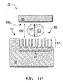
apparatus 700 after forming a secondmechanical structure 905 having a secondrigid surface 910. In some instances, the secondmechanical structure 905 comprises a second semiconductor substrate such as a silicon wafer. In some cases, as shown, the secondrigid surface 910 is planar, although in other cases a portion of the secondrigid surface 910 is patterned to form a nanostructure that can be the same or different than thenanostructure 805 of the firstrigid surface 710. - As further illustrated in FIGURE 10, the second
mechanical structure 905 is positioned to oppose the firstmechanical structure 705. The secondmechanical structure 905 is cooperable with thenanostructure 805 such that amicroscopic particle 1005 is locatable between thenanostructure 805 and the secondrigid surface 910. For instance, positioning can include adjusting adistance 1010 between thenanostructure 805 and the secondrigid surface 910 to be less than about 2 times anaverage diameter 1015 of themicroparticle 1005. - Although the present invention has been described in detail, those of ordinary skill in the art should understand that they can make various changes, substitutions and alterations herein without departing from the scope of the invention.
Claims (10)
- An apparatus, comprising:a first mechanical structure having a first rigid surface, an area of said first rigid surface having a nanostructured surface; anda second mechanical structure having a second rigid surface and opposing said first mechanical structure and cooperable with said nanostructured surface such that a microscopic particle is locatable between said nanostructured surface and said second rigid surface.
- The apparatus of claim 1, wherein said nanostructured surface comprises pins configured to have a pitch equal to smaller than about one-half of an average diameter of said microscopic particle.
- The apparatus of claim 1, wherein one or both of said first rigid surface and said second rigid surface are movable with respect to each other and cooperable to apply a contact force to said microscopic particle through said nanostructured surface.
- The apparatus of claim 1, wherein said nanostructured surface comprises pins having a conductive core, said conductive core and said second rigid surface being electrically coupled to a voltage source.
- The apparatus of claim 1, wherein said nanostructured surface comprises pins having an insulated conductive core, said conductive core and said second rigid surface being electrically coupled to a voltage source.
- The apparatus of claim 1, further comprising a device configured to generate an acoustic wave that is passed to at least one of said first rigid surface or said second rigid surface.
- The apparatus of claim 1, wherein said nanostructured surface comprises a plurality of blades having a diameter configured to rupture a membrane of said microparticle.
- The apparatus of claim 1, further comprising a system configured to analyze material released from said microparticle when said microparticle is ruptured.
- The apparatus of claim 1, wherein one or both of said first rigid surface or said second rigid surface further comprise openings to form a permeable membrane.
- The apparatus of claim 9, wherein said area of said first rigid surface includes said openings.
Applications Claiming Priority (1)
| Application Number | Priority Date | Filing Date | Title |
|---|---|---|---|
| US10/954,552 US7608446B2 (en) | 2004-09-30 | 2004-09-30 | Nanostructured surface for microparticle analysis and manipulation |
Publications (2)
| Publication Number | Publication Date |
|---|---|
| EP1642962A1 true EP1642962A1 (en) | 2006-04-05 |
| EP1642962B1 EP1642962B1 (en) | 2007-10-31 |
Family
ID=35448186
Family Applications (1)
| Application Number | Title | Priority Date | Filing Date |
|---|---|---|---|
| EP05255909A Expired - Fee Related EP1642962B1 (en) | 2004-09-30 | 2005-09-22 | Nanostructured surface for microparticle analysis and manipulation |
Country Status (4)
| Country | Link |
|---|---|
| US (2) | US7608446B2 (en) |
| EP (1) | EP1642962B1 (en) |
| JP (1) | JP4977350B2 (en) |
| DE (1) | DE602005003086T2 (en) |
Cited By (1)
| Publication number | Priority date | Publication date | Assignee | Title |
|---|---|---|---|---|
| US20120256027A1 (en) * | 2009-12-18 | 2012-10-11 | Gwangju Institute Of Science And Technology | Cell lysis apparatus and manufacturing method thereof |
Families Citing this family (8)
| Publication number | Priority date | Publication date | Assignee | Title |
|---|---|---|---|---|
| US7727293B2 (en) * | 2005-02-25 | 2010-06-01 | SOCIéTé BIC | Hydrogen generating fuel cell cartridges |
| US20080138581A1 (en) * | 2006-07-17 | 2008-06-12 | Rajmohan Bhandari | Masking high-aspect aspect ratio structures |
| DE102007019842A1 (en) * | 2007-04-25 | 2008-10-30 | Forschungsinstitut Für Die Biologie Landwirtschaftlicher Nutztiere | Method and arrangement for electrically contacting a membrane-encased object with an electrode |
| US7898096B1 (en) * | 2007-08-22 | 2011-03-01 | Thomas Nikita Krupenkin | Method and apparatus for energy harvesting using microfluidics |
| FR2921185B1 (en) * | 2007-09-17 | 2009-10-30 | Univ D Auvergne Clermont 1 Eta | APPARATUS FOR SIMULATION OF MASTICATION IN A MAMMALIAN |
| US8785177B2 (en) | 2011-11-04 | 2014-07-22 | The Board Of Trustees Of The University Of Illinois, A Body Corporate And Politic Of The State Of Illinois | Methods for nano-mechanoporation |
| US10468124B2 (en) | 2012-01-23 | 2019-11-05 | Toyota Motor Engineering & Manufacturing North America, Inc. | Process for designing and producing cooling fluids |
| US20230407235A1 (en) * | 2020-11-12 | 2023-12-21 | The University Of Chicago | Microfluidic and mems cell lysis system and method |
Citations (7)
| Publication number | Priority date | Publication date | Assignee | Title |
|---|---|---|---|---|
| WO1999025816A1 (en) * | 1997-11-14 | 1999-05-27 | California Institute Of Technology | Cell lysis device |
| US6100084A (en) * | 1998-11-05 | 2000-08-08 | The Regents Of The University Of California | Micro-sonicator for spore lysis |
| US20020185557A1 (en) * | 2001-06-06 | 2002-12-12 | Integrates Sensing Systems | Micromachined lysing device and method for performing cell lysis |
| WO2003037781A1 (en) * | 2000-10-02 | 2003-05-08 | Motorola, Inc. | Microfluidic devices having embedded metal conductors and methods of fabricating said devices |
| WO2003055976A2 (en) * | 2001-10-04 | 2003-07-10 | Cepheid | Apparatus and method for rapid disruption of cells or viruses |
| WO2004021083A1 (en) * | 2002-08-27 | 2004-03-11 | Obducat Ab | Device for transferring a pattern to an object |
| EP1584375A1 (en) * | 2004-03-23 | 2005-10-12 | Lucent Technologies Inc. | Dynamically controllable biological/chemical detectors having nanostructured surfaces |
Family Cites Families (35)
| Publication number | Priority date | Publication date | Assignee | Title |
|---|---|---|---|---|
| JPS4317677Y1 (en) * | 1965-10-01 | 1968-07-22 | ||
| JPS62151174A (en) * | 1985-12-24 | 1987-07-06 | Akira Mizuno | Cell disintegration apparatus using high-voltage pulse |
| JPS62130498U (en) * | 1986-02-13 | 1987-08-18 | ||
| JPH04112784A (en) * | 1990-08-31 | 1992-04-14 | Shimadzu Corp | Ultrasonic crusher |
| US5457041A (en) * | 1994-03-25 | 1995-10-10 | Science Applications International Corporation | Needle array and method of introducing biological substances into living cells using the needle array |
| US5674592A (en) | 1995-05-04 | 1997-10-07 | Minnesota Mining And Manufacturing Company | Functionalized nanostructured films |
| JPH09149783A (en) * | 1995-11-30 | 1997-06-10 | Eiken Kizai Kk | Homogenizer for examination of microorganism |
| EP0927331B1 (en) * | 1996-08-08 | 2004-03-31 | William Marsh Rice University | Macroscopically manipulable nanoscale devices made from nanotube assemblies |
| DE19729028C1 (en) * | 1997-07-08 | 1999-05-06 | Fraunhofer Ges Forschung | Device and method for isolating cell material from a tissue association and / or a liquid |
| EP1004015B1 (en) | 1997-08-15 | 2004-01-02 | Alexion Pharmaceuticals, Inc. | Apparatus for performing assays at reaction sites |
| DE19752961C1 (en) * | 1997-11-28 | 1999-07-15 | Fraunhofer Ges Forschung | Method and device for disrupting biological cells for extracting and analyzing the cell contents |
| US6719868B1 (en) | 1998-03-23 | 2004-04-13 | President And Fellows Of Harvard College | Methods for fabricating microfluidic structures |
| FI980874A (en) | 1998-04-20 | 1999-10-21 | Wallac Oy | Method and apparatus for conducting chemical analysis on small amounts of liquid |
| US6185961B1 (en) | 1999-01-27 | 2001-02-13 | The United States Of America As Represented By The Secretary Of The Navy | Nanopost arrays and process for making same |
| US6350397B1 (en) | 1999-03-10 | 2002-02-26 | Aspen Research Corporation | Optical member with layer having a coating geometry and composition that enhance cleaning properties |
| US6451264B1 (en) | 2000-01-28 | 2002-09-17 | Roche Diagnostics Corporation | Fluid flow control in curved capillary channels |
| EP1261862A2 (en) | 2000-02-22 | 2002-12-04 | California Institute of Technology | Development of a gel-free molecular sieve based on self-assembled nano-arrays |
| US6645757B1 (en) * | 2001-02-08 | 2003-11-11 | Sandia Corporation | Apparatus and method for transforming living cells |
| WO2002065515A2 (en) | 2001-02-14 | 2002-08-22 | Science & Technology Corporation @ Unm | Nanostructured devices for separation and analysis |
| ITMI20011665A1 (en) * | 2001-07-31 | 2003-01-31 | Mamiliano Dini | TETRASSIAL FABRIC AND MACHINE FOR ITS PRODUCTION |
| US6783647B2 (en) | 2001-10-19 | 2004-08-31 | Ut-Battelle, Llc | Microfluidic systems and methods of transport and lysis of cells and analysis of cell lysate |
| US6894359B2 (en) * | 2002-09-04 | 2005-05-17 | Nanomix, Inc. | Sensitivity control for nanotube sensors |
| SE0201738D0 (en) | 2002-06-07 | 2002-06-07 | Aamic Ab | Micro-fluid structures |
| JP2004037187A (en) * | 2002-07-02 | 2004-02-05 | Mishima Daiji | Ultrasonic vibration supplying apparatus and its supply method |
| WO2004036202A1 (en) * | 2002-10-16 | 2004-04-29 | Cellectricon Ab | Nanoelectrodes and nanotips for recording transmembrane currents in a plurality of cells |
| US7641863B2 (en) | 2003-03-06 | 2010-01-05 | Ut-Battelle Llc | Nanoengineered membranes for controlled transport |
| US20040191127A1 (en) | 2003-03-31 | 2004-09-30 | Avinoam Kornblit | Method and apparatus for controlling the movement of a liquid on a nanostructured or microstructured surface |
| US7156032B2 (en) | 2003-08-22 | 2007-01-02 | Lucent Technologies Inc. | Method and apparatus for controlling friction between a fluid and a body |
| US7067328B2 (en) * | 2003-09-25 | 2006-06-27 | Nanosys, Inc. | Methods, devices and compositions for depositing and orienting nanostructures |
| US8124423B2 (en) | 2003-09-30 | 2012-02-28 | Alcatel Lucent | Method and apparatus for controlling the flow resistance of a fluid on nanostructured or microstructured surfaces |
| US7227235B2 (en) | 2003-11-18 | 2007-06-05 | Lucent Technologies Inc. | Electrowetting battery having a nanostructured electrode surface |
| US8915957B2 (en) | 2004-03-11 | 2014-12-23 | Alcatel Lucent | Drug delivery stent |
| US7749646B2 (en) | 2004-03-18 | 2010-07-06 | Alcatel-Lucent Usa Inc. | Reversibly-activated nanostructured battery |
| US20050211505A1 (en) | 2004-03-26 | 2005-09-29 | Kroupenkine Timofei N | Nanostructured liquid bearing |
| US7005593B2 (en) | 2004-04-01 | 2006-02-28 | Lucent Technologies Inc. | Liquid electrical microswitch |
-
2004
- 2004-09-30 US US10/954,552 patent/US7608446B2/en not_active Expired - Fee Related
-
2005
- 2005-09-22 DE DE602005003086T patent/DE602005003086T2/en active Active
- 2005-09-22 EP EP05255909A patent/EP1642962B1/en not_active Expired - Fee Related
- 2005-09-28 JP JP2005281351A patent/JP4977350B2/en active Active
-
2009
- 2009-08-12 US US12/540,162 patent/US7960167B2/en not_active Expired - Fee Related
Patent Citations (7)
| Publication number | Priority date | Publication date | Assignee | Title |
|---|---|---|---|---|
| WO1999025816A1 (en) * | 1997-11-14 | 1999-05-27 | California Institute Of Technology | Cell lysis device |
| US6100084A (en) * | 1998-11-05 | 2000-08-08 | The Regents Of The University Of California | Micro-sonicator for spore lysis |
| WO2003037781A1 (en) * | 2000-10-02 | 2003-05-08 | Motorola, Inc. | Microfluidic devices having embedded metal conductors and methods of fabricating said devices |
| US20020185557A1 (en) * | 2001-06-06 | 2002-12-12 | Integrates Sensing Systems | Micromachined lysing device and method for performing cell lysis |
| WO2003055976A2 (en) * | 2001-10-04 | 2003-07-10 | Cepheid | Apparatus and method for rapid disruption of cells or viruses |
| WO2004021083A1 (en) * | 2002-08-27 | 2004-03-11 | Obducat Ab | Device for transferring a pattern to an object |
| EP1584375A1 (en) * | 2004-03-23 | 2005-10-12 | Lucent Technologies Inc. | Dynamically controllable biological/chemical detectors having nanostructured surfaces |
Non-Patent Citations (1)
| Title |
|---|
| CARLO DI D ET AL: "MECHANICAL CELL LYSIS RESULTS OF A SAMPLE PREPARATION MODULE FOR FUNCTIONAL GENOMICS", ANNUAL INTERNATIONAL IEEE-EMBS SPECIAL TOPIC CONFERENCE ON MICROTECHNOLOGIES IN MEDICINE AND BIOLOGY. PROCEEDINGS, 2 May 2002 (2002-05-02), pages 527 - 530, XP001180619 * |
Cited By (2)
| Publication number | Priority date | Publication date | Assignee | Title |
|---|---|---|---|---|
| US20120256027A1 (en) * | 2009-12-18 | 2012-10-11 | Gwangju Institute Of Science And Technology | Cell lysis apparatus and manufacturing method thereof |
| US9506028B2 (en) * | 2009-12-18 | 2016-11-29 | Gwangju Institute Of Science And Technology | Mechanical cell lysis apparatus |
Also Published As
| Publication number | Publication date |
|---|---|
| DE602005003086D1 (en) | 2007-12-13 |
| US7960167B2 (en) | 2011-06-14 |
| US20090295408A1 (en) | 2009-12-03 |
| US7608446B2 (en) | 2009-10-27 |
| US20060068487A1 (en) | 2006-03-30 |
| JP2006105980A (en) | 2006-04-20 |
| JP4977350B2 (en) | 2012-07-18 |
| EP1642962B1 (en) | 2007-10-31 |
| DE602005003086T2 (en) | 2008-10-02 |
Similar Documents
| Publication | Publication Date | Title |
|---|---|---|
| US7960167B2 (en) | Nanostructured surface for microparticle analysis and manipulation | |
| US20190346358A1 (en) | Active micro sieve and methods for biological applications | |
| Zhang et al. | Dielectrophoresis for manipulation of micro/nano particles in microfluidic systems | |
| US20060188904A1 (en) | Biosensors having single reactant components immobilized over single electrodes and methods of making and using thereof | |
| US7088116B1 (en) | Optoelectronic probe | |
| Hashiguchi et al. | DNA manipulation and retrieval from an aqueous solution with micromachined nanotweezers | |
| US20120058504A1 (en) | Methods and apparatus for dielectrophoretic shuttling and measurement of single cells or other particles in microfluidic chips | |
| US8524063B2 (en) | Micro-electrode device for dielectrophoretic characterisation of particles | |
| Zheng et al. | Towards single molecule manipulation with dielectrophoresis using nanoelectrodes | |
| JP2001500252A (en) | Apparatus and method for testing particles using dielectrophoresis | |
| WO2006004558A1 (en) | Biochip for sorting and lysing biological samples | |
| JP7108548B2 (en) | Methods and devices for analyzing nucleic acid molecules | |
| US20190001320A1 (en) | Biological detection system | |
| Otto et al. | Dielectrophoretic immobilisation of antibodies on microelectrode arrays | |
| JP2019525186A (en) | Reconfigurable surface-enhanced Raman spectroscopy device and method therefor | |
| US8262885B2 (en) | Dielectrophoretic tweezers apparatus and methods | |
| US20140166483A1 (en) | Electrokinetics-assisted sensor | |
| Zhou et al. | Spatial manipulation and assembly of nanoparticles by atomic force microscopy tip-induced dielectrophoresis | |
| Buyong et al. | Design, fabrication and characterization of dielectrophoretic microelectrode array for particle capture | |
| Deng et al. | Controllable fabrication of pyramidal silicon nanopore arrays and nanoslits for nanostencil lithography | |
| Ghomian et al. | Review of dielectrophoretic manipulation of micro and nanomaterials: Fundamentals, recent developments, and challenges | |
| EP2673093B1 (en) | Method and microsystem for detecting analytes which are present in drops of liquid. | |
| EP3801916A1 (en) | Graphene-based dielectrophoresis sensor and method | |
| Abd Samad et al. | Dielectrophoresis velocities response on tapered electrode profile: Simulation and experimental | |
| EP2052784A1 (en) | Barrier layer over electrodes of electrically active loc devices |
Legal Events
| Date | Code | Title | Description |
|---|---|---|---|
| PUAI | Public reference made under article 153(3) epc to a published international application that has entered the european phase |
Free format text: ORIGINAL CODE: 0009012 |
|
| 17P | Request for examination filed |
Effective date: 20051006 |
|
| AK | Designated contracting states |
Kind code of ref document: A1 Designated state(s): AT BE BG CH CY CZ DE DK EE ES FI FR GB GR HU IE IS IT LI LT LU LV MC NL PL PT RO SE SI SK TR |
|
| AX | Request for extension of the european patent |
Extension state: AL BA HR MK YU |
|
| 17Q | First examination report despatched |
Effective date: 20060207 |
|
| AKX | Designation fees paid |
Designated state(s): DE FR GB |
|
| GRAP | Despatch of communication of intention to grant a patent |
Free format text: ORIGINAL CODE: EPIDOSNIGR1 |
|
| GRAS | Grant fee paid |
Free format text: ORIGINAL CODE: EPIDOSNIGR3 |
|
| GRAA | (expected) grant |
Free format text: ORIGINAL CODE: 0009210 |
|
| AK | Designated contracting states |
Kind code of ref document: B1 Designated state(s): DE FR GB |
|
| REG | Reference to a national code |
Ref country code: GB Ref legal event code: FG4D |
|
| REF | Corresponds to: |
Ref document number: 602005003086 Country of ref document: DE Date of ref document: 20071213 Kind code of ref document: P |
|
| ET | Fr: translation filed | ||
| PLBE | No opposition filed within time limit |
Free format text: ORIGINAL CODE: 0009261 |
|
| STAA | Information on the status of an ep patent application or granted ep patent |
Free format text: STATUS: NO OPPOSITION FILED WITHIN TIME LIMIT |
|
| 26N | No opposition filed |
Effective date: 20080801 |
|
| REG | Reference to a national code |
Ref country code: GB Ref legal event code: 732E Free format text: REGISTERED BETWEEN 20131107 AND 20131113 |
|
| REG | Reference to a national code |
Ref country code: FR Ref legal event code: CD Owner name: ALCATEL-LUCENT USA INC. Effective date: 20131122 |
|
| REG | Reference to a national code |
Ref country code: FR Ref legal event code: GC Effective date: 20140410 |
|
| REG | Reference to a national code |
Ref country code: FR Ref legal event code: RG Effective date: 20141015 |
|
| REG | Reference to a national code |
Ref country code: FR Ref legal event code: PLFP Year of fee payment: 11 |
|
| REG | Reference to a national code |
Ref country code: FR Ref legal event code: PLFP Year of fee payment: 12 |
|
| REG | Reference to a national code |
Ref country code: FR Ref legal event code: PLFP Year of fee payment: 13 |
|
| REG | Reference to a national code |
Ref country code: FR Ref legal event code: PLFP Year of fee payment: 14 |
|
| PGFP | Annual fee paid to national office [announced via postgrant information from national office to epo] |
Ref country code: GB Payment date: 20200909 Year of fee payment: 16 Ref country code: FR Payment date: 20200812 Year of fee payment: 16 Ref country code: DE Payment date: 20200909 Year of fee payment: 16 |
|
| REG | Reference to a national code |
Ref country code: DE Ref legal event code: R119 Ref document number: 602005003086 Country of ref document: DE |
|
| GBPC | Gb: european patent ceased through non-payment of renewal fee |
Effective date: 20210922 |
|
| PG25 | Lapsed in a contracting state [announced via postgrant information from national office to epo] |
Ref country code: GB Free format text: LAPSE BECAUSE OF NON-PAYMENT OF DUE FEES Effective date: 20210922 Ref country code: FR Free format text: LAPSE BECAUSE OF NON-PAYMENT OF DUE FEES Effective date: 20210930 Ref country code: DE Free format text: LAPSE BECAUSE OF NON-PAYMENT OF DUE FEES Effective date: 20220401 |