EP1650031B1 - Ink jet nozzle with slotted sidewall and moveable vane - Google Patents
Ink jet nozzle with slotted sidewall and moveable vane Download PDFInfo
- Publication number
- EP1650031B1 EP1650031B1 EP05109756A EP05109756A EP1650031B1 EP 1650031 B1 EP1650031 B1 EP 1650031B1 EP 05109756 A EP05109756 A EP 05109756A EP 05109756 A EP05109756 A EP 05109756A EP 1650031 B1 EP1650031 B1 EP 1650031B1
- Authority
- EP
- European Patent Office
- Prior art keywords
- ink jet
- ink
- actuator
- jet nozzle
- nozzle chamber
- Prior art date
- Legal status (The legal status is an assumption and is not a legal conclusion. Google has not performed a legal analysis and makes no representation as to the accuracy of the status listed.)
- Expired - Lifetime
Links
- 239000000463 material Substances 0.000 claims description 22
- XUIMIQQOPSSXEZ-UHFFFAOYSA-N Silicon Chemical compound [Si] XUIMIQQOPSSXEZ-UHFFFAOYSA-N 0.000 claims description 12
- 229910052710 silicon Inorganic materials 0.000 claims description 12
- 239000010703 silicon Substances 0.000 claims description 12
- 238000010438 heat treatment Methods 0.000 claims description 4
- 239000000758 substrate Substances 0.000 claims description 3
- 238000005530 etching Methods 0.000 claims description 2
- 230000002209 hydrophobic effect Effects 0.000 claims description 2
- 239000004020 conductor Substances 0.000 claims 1
- 235000012431 wafers Nutrition 0.000 description 17
- 239000010410 layer Substances 0.000 description 15
- 238000007641 inkjet printing Methods 0.000 description 14
- 238000000034 method Methods 0.000 description 14
- 238000004519 manufacturing process Methods 0.000 description 11
- 238000010276 construction Methods 0.000 description 10
- 238000005516 engineering process Methods 0.000 description 9
- NRTOMJZYCJJWKI-UHFFFAOYSA-N Titanium nitride Chemical compound [Ti]#N NRTOMJZYCJJWKI-UHFFFAOYSA-N 0.000 description 7
- 238000007639 printing Methods 0.000 description 7
- 230000007246 mechanism Effects 0.000 description 6
- 230000008569 process Effects 0.000 description 6
- 238000012545 processing Methods 0.000 description 5
- RTAQQCXQSZGOHL-UHFFFAOYSA-N Titanium Chemical compound [Ti] RTAQQCXQSZGOHL-UHFFFAOYSA-N 0.000 description 4
- 238000005452 bending Methods 0.000 description 4
- 239000010936 titanium Substances 0.000 description 4
- 229910052719 titanium Inorganic materials 0.000 description 4
- 230000008901 benefit Effects 0.000 description 3
- KRHYYFGTRYWZRS-UHFFFAOYSA-N Fluorane Chemical compound F KRHYYFGTRYWZRS-UHFFFAOYSA-N 0.000 description 2
- PXHVJJICTQNCMI-UHFFFAOYSA-N Nickel Chemical compound [Ni] PXHVJJICTQNCMI-UHFFFAOYSA-N 0.000 description 2
- VYPSYNLAJGMNEJ-UHFFFAOYSA-N Silicium dioxide Chemical compound O=[Si]=O VYPSYNLAJGMNEJ-UHFFFAOYSA-N 0.000 description 2
- 229910052782 aluminium Inorganic materials 0.000 description 2
- XAGFODPZIPBFFR-UHFFFAOYSA-N aluminium Chemical compound [Al] XAGFODPZIPBFFR-UHFFFAOYSA-N 0.000 description 2
- 235000009508 confectionery Nutrition 0.000 description 2
- 238000010586 diagram Methods 0.000 description 2
- 239000012530 fluid Substances 0.000 description 2
- 229910052751 metal Inorganic materials 0.000 description 2
- 239000002184 metal Substances 0.000 description 2
- 238000001020 plasma etching Methods 0.000 description 2
- 239000004065 semiconductor Substances 0.000 description 2
- QYEXBYZXHDUPRC-UHFFFAOYSA-N B#[Ti]#B Chemical compound B#[Ti]#B QYEXBYZXHDUPRC-UHFFFAOYSA-N 0.000 description 1
- 101100269850 Caenorhabditis elegans mask-1 gene Proteins 0.000 description 1
- 229910052581 Si3N4 Inorganic materials 0.000 description 1
- 239000004809 Teflon Substances 0.000 description 1
- 229920006362 Teflon® Polymers 0.000 description 1
- 229910033181 TiB2 Inorganic materials 0.000 description 1
- 230000004913 activation Effects 0.000 description 1
- 239000003086 colorant Substances 0.000 description 1
- 239000013078 crystal Substances 0.000 description 1
- 238000013461 design Methods 0.000 description 1
- 238000009826 distribution Methods 0.000 description 1
- 230000000694 effects Effects 0.000 description 1
- 238000005323 electroforming Methods 0.000 description 1
- 230000005686 electrostatic field Effects 0.000 description 1
- 230000004907 flux Effects 0.000 description 1
- 239000011521 glass Substances 0.000 description 1
- 230000001939 inductive effect Effects 0.000 description 1
- 238000000608 laser ablation Methods 0.000 description 1
- 238000007648 laser printing Methods 0.000 description 1
- 239000007788 liquid Substances 0.000 description 1
- 230000007774 longterm Effects 0.000 description 1
- 238000003754 machining Methods 0.000 description 1
- 238000007567 mass-production technique Methods 0.000 description 1
- 239000011159 matrix material Substances 0.000 description 1
- 238000005259 measurement Methods 0.000 description 1
- 238000005459 micromachining Methods 0.000 description 1
- 239000002991 molded plastic Substances 0.000 description 1
- 229910052759 nickel Inorganic materials 0.000 description 1
- 238000007645 offset printing Methods 0.000 description 1
- 230000003287 optical effect Effects 0.000 description 1
- 238000004806 packaging method and process Methods 0.000 description 1
- 238000002161 passivation Methods 0.000 description 1
- 239000011241 protective layer Substances 0.000 description 1
- 238000004080 punching Methods 0.000 description 1
- 230000009467 reduction Effects 0.000 description 1
- 239000000523 sample Substances 0.000 description 1
- 238000000926 separation method Methods 0.000 description 1
- 235000012239 silicon dioxide Nutrition 0.000 description 1
- 239000000377 silicon dioxide Substances 0.000 description 1
- HQVNEWCFYHHQES-UHFFFAOYSA-N silicon nitride Chemical compound N12[Si]34N5[Si]62N3[Si]51N64 HQVNEWCFYHHQES-UHFFFAOYSA-N 0.000 description 1
- 230000003068 static effect Effects 0.000 description 1
- 238000000859 sublimation Methods 0.000 description 1
- 230000008022 sublimation Effects 0.000 description 1
- 238000012360 testing method Methods 0.000 description 1
- 238000007514 turning Methods 0.000 description 1
Images


Classifications
-
- B—PERFORMING OPERATIONS; TRANSPORTING
- B41—PRINTING; LINING MACHINES; TYPEWRITERS; STAMPS
- B41J—TYPEWRITERS; SELECTIVE PRINTING MECHANISMS, i.e. MECHANISMS PRINTING OTHERWISE THAN FROM A FORME; CORRECTION OF TYPOGRAPHICAL ERRORS
- B41J3/00—Typewriters or selective printing or marking mechanisms characterised by the purpose for which they are constructed
- B41J3/44—Typewriters or selective printing mechanisms having dual functions or combined with, or coupled to, apparatus performing other functions
- B41J3/445—Printers integrated in other types of apparatus, e.g. printers integrated in cameras
-
- B—PERFORMING OPERATIONS; TRANSPORTING
- B41—PRINTING; LINING MACHINES; TYPEWRITERS; STAMPS
- B41J—TYPEWRITERS; SELECTIVE PRINTING MECHANISMS, i.e. MECHANISMS PRINTING OTHERWISE THAN FROM A FORME; CORRECTION OF TYPOGRAPHICAL ERRORS
- B41J2/00—Typewriters or selective printing mechanisms characterised by the printing or marking process for which they are designed
- B41J2/005—Typewriters or selective printing mechanisms characterised by the printing or marking process for which they are designed characterised by bringing liquid or particles selectively into contact with a printing material
- B41J2/01—Ink jet
- B41J2/135—Nozzles
- B41J2/14—Structure thereof only for on-demand ink jet heads
- B41J2/14314—Structure of ink jet print heads with electrostatically actuated membrane
-
- B—PERFORMING OPERATIONS; TRANSPORTING
- B41—PRINTING; LINING MACHINES; TYPEWRITERS; STAMPS
- B41J—TYPEWRITERS; SELECTIVE PRINTING MECHANISMS, i.e. MECHANISMS PRINTING OTHERWISE THAN FROM A FORME; CORRECTION OF TYPOGRAPHICAL ERRORS
- B41J2/00—Typewriters or selective printing mechanisms characterised by the printing or marking process for which they are designed
- B41J2/005—Typewriters or selective printing mechanisms characterised by the printing or marking process for which they are designed characterised by bringing liquid or particles selectively into contact with a printing material
- B41J2/01—Ink jet
- B41J2/135—Nozzles
- B41J2/14—Structure thereof only for on-demand ink jet heads
- B41J2/14427—Structure of ink jet print heads with thermal bend detached actuators
-
- B—PERFORMING OPERATIONS; TRANSPORTING
- B41—PRINTING; LINING MACHINES; TYPEWRITERS; STAMPS
- B41J—TYPEWRITERS; SELECTIVE PRINTING MECHANISMS, i.e. MECHANISMS PRINTING OTHERWISE THAN FROM A FORME; CORRECTION OF TYPOGRAPHICAL ERRORS
- B41J2/00—Typewriters or selective printing mechanisms characterised by the printing or marking process for which they are designed
- B41J2/005—Typewriters or selective printing mechanisms characterised by the printing or marking process for which they are designed characterised by bringing liquid or particles selectively into contact with a printing material
- B41J2/01—Ink jet
- B41J2/135—Nozzles
- B41J2/16—Production of nozzles
- B41J2/1621—Manufacturing processes
- B41J2/1623—Manufacturing processes bonding and adhesion
-
- B—PERFORMING OPERATIONS; TRANSPORTING
- B41—PRINTING; LINING MACHINES; TYPEWRITERS; STAMPS
- B41J—TYPEWRITERS; SELECTIVE PRINTING MECHANISMS, i.e. MECHANISMS PRINTING OTHERWISE THAN FROM A FORME; CORRECTION OF TYPOGRAPHICAL ERRORS
- B41J2/00—Typewriters or selective printing mechanisms characterised by the printing or marking process for which they are designed
- B41J2/005—Typewriters or selective printing mechanisms characterised by the printing or marking process for which they are designed characterised by bringing liquid or particles selectively into contact with a printing material
- B41J2/01—Ink jet
- B41J2/135—Nozzles
- B41J2/16—Production of nozzles
- B41J2/1621—Manufacturing processes
- B41J2/1626—Manufacturing processes etching
- B41J2/1628—Manufacturing processes etching dry etching
-
- B—PERFORMING OPERATIONS; TRANSPORTING
- B41—PRINTING; LINING MACHINES; TYPEWRITERS; STAMPS
- B41J—TYPEWRITERS; SELECTIVE PRINTING MECHANISMS, i.e. MECHANISMS PRINTING OTHERWISE THAN FROM A FORME; CORRECTION OF TYPOGRAPHICAL ERRORS
- B41J2/00—Typewriters or selective printing mechanisms characterised by the printing or marking process for which they are designed
- B41J2/005—Typewriters or selective printing mechanisms characterised by the printing or marking process for which they are designed characterised by bringing liquid or particles selectively into contact with a printing material
- B41J2/01—Ink jet
- B41J2/135—Nozzles
- B41J2/16—Production of nozzles
- B41J2/1621—Manufacturing processes
- B41J2/1626—Manufacturing processes etching
- B41J2/1629—Manufacturing processes etching wet etching
-
- B—PERFORMING OPERATIONS; TRANSPORTING
- B41—PRINTING; LINING MACHINES; TYPEWRITERS; STAMPS
- B41J—TYPEWRITERS; SELECTIVE PRINTING MECHANISMS, i.e. MECHANISMS PRINTING OTHERWISE THAN FROM A FORME; CORRECTION OF TYPOGRAPHICAL ERRORS
- B41J2/00—Typewriters or selective printing mechanisms characterised by the printing or marking process for which they are designed
- B41J2/005—Typewriters or selective printing mechanisms characterised by the printing or marking process for which they are designed characterised by bringing liquid or particles selectively into contact with a printing material
- B41J2/01—Ink jet
- B41J2/135—Nozzles
- B41J2/16—Production of nozzles
- B41J2/1621—Manufacturing processes
- B41J2/1631—Manufacturing processes photolithography
-
- B—PERFORMING OPERATIONS; TRANSPORTING
- B41—PRINTING; LINING MACHINES; TYPEWRITERS; STAMPS
- B41J—TYPEWRITERS; SELECTIVE PRINTING MECHANISMS, i.e. MECHANISMS PRINTING OTHERWISE THAN FROM A FORME; CORRECTION OF TYPOGRAPHICAL ERRORS
- B41J2/00—Typewriters or selective printing mechanisms characterised by the printing or marking process for which they are designed
- B41J2/005—Typewriters or selective printing mechanisms characterised by the printing or marking process for which they are designed characterised by bringing liquid or particles selectively into contact with a printing material
- B41J2/01—Ink jet
- B41J2/135—Nozzles
- B41J2/16—Production of nozzles
- B41J2/1621—Manufacturing processes
- B41J2/1632—Manufacturing processes machining
-
- B—PERFORMING OPERATIONS; TRANSPORTING
- B41—PRINTING; LINING MACHINES; TYPEWRITERS; STAMPS
- B41J—TYPEWRITERS; SELECTIVE PRINTING MECHANISMS, i.e. MECHANISMS PRINTING OTHERWISE THAN FROM A FORME; CORRECTION OF TYPOGRAPHICAL ERRORS
- B41J2/00—Typewriters or selective printing mechanisms characterised by the printing or marking process for which they are designed
- B41J2/005—Typewriters or selective printing mechanisms characterised by the printing or marking process for which they are designed characterised by bringing liquid or particles selectively into contact with a printing material
- B41J2/01—Ink jet
- B41J2/135—Nozzles
- B41J2/16—Production of nozzles
- B41J2/1621—Manufacturing processes
- B41J2/1635—Manufacturing processes dividing the wafer into individual chips
-
- B—PERFORMING OPERATIONS; TRANSPORTING
- B41—PRINTING; LINING MACHINES; TYPEWRITERS; STAMPS
- B41J—TYPEWRITERS; SELECTIVE PRINTING MECHANISMS, i.e. MECHANISMS PRINTING OTHERWISE THAN FROM A FORME; CORRECTION OF TYPOGRAPHICAL ERRORS
- B41J2/00—Typewriters or selective printing mechanisms characterised by the printing or marking process for which they are designed
- B41J2/005—Typewriters or selective printing mechanisms characterised by the printing or marking process for which they are designed characterised by bringing liquid or particles selectively into contact with a printing material
- B41J2/01—Ink jet
- B41J2/135—Nozzles
- B41J2/16—Production of nozzles
- B41J2/1621—Manufacturing processes
- B41J2/1637—Manufacturing processes molding
- B41J2/1639—Manufacturing processes molding sacrificial molding
-
- B—PERFORMING OPERATIONS; TRANSPORTING
- B41—PRINTING; LINING MACHINES; TYPEWRITERS; STAMPS
- B41J—TYPEWRITERS; SELECTIVE PRINTING MECHANISMS, i.e. MECHANISMS PRINTING OTHERWISE THAN FROM A FORME; CORRECTION OF TYPOGRAPHICAL ERRORS
- B41J2/00—Typewriters or selective printing mechanisms characterised by the printing or marking process for which they are designed
- B41J2/005—Typewriters or selective printing mechanisms characterised by the printing or marking process for which they are designed characterised by bringing liquid or particles selectively into contact with a printing material
- B41J2/01—Ink jet
- B41J2/135—Nozzles
- B41J2/16—Production of nozzles
- B41J2/1621—Manufacturing processes
- B41J2/164—Manufacturing processes thin film formation
- B41J2/1642—Manufacturing processes thin film formation thin film formation by CVD [chemical vapor deposition]
-
- B—PERFORMING OPERATIONS; TRANSPORTING
- B41—PRINTING; LINING MACHINES; TYPEWRITERS; STAMPS
- B41J—TYPEWRITERS; SELECTIVE PRINTING MECHANISMS, i.e. MECHANISMS PRINTING OTHERWISE THAN FROM A FORME; CORRECTION OF TYPOGRAPHICAL ERRORS
- B41J2/00—Typewriters or selective printing mechanisms characterised by the printing or marking process for which they are designed
- B41J2/005—Typewriters or selective printing mechanisms characterised by the printing or marking process for which they are designed characterised by bringing liquid or particles selectively into contact with a printing material
- B41J2/01—Ink jet
- B41J2/135—Nozzles
- B41J2/16—Production of nozzles
- B41J2/1621—Manufacturing processes
- B41J2/164—Manufacturing processes thin film formation
- B41J2/1643—Manufacturing processes thin film formation thin film formation by plating
-
- B—PERFORMING OPERATIONS; TRANSPORTING
- B41—PRINTING; LINING MACHINES; TYPEWRITERS; STAMPS
- B41J—TYPEWRITERS; SELECTIVE PRINTING MECHANISMS, i.e. MECHANISMS PRINTING OTHERWISE THAN FROM A FORME; CORRECTION OF TYPOGRAPHICAL ERRORS
- B41J2/00—Typewriters or selective printing mechanisms characterised by the printing or marking process for which they are designed
- B41J2/005—Typewriters or selective printing mechanisms characterised by the printing or marking process for which they are designed characterised by bringing liquid or particles selectively into contact with a printing material
- B41J2/01—Ink jet
- B41J2/135—Nozzles
- B41J2/16—Production of nozzles
- B41J2/1621—Manufacturing processes
- B41J2/164—Manufacturing processes thin film formation
- B41J2/1645—Manufacturing processes thin film formation thin film formation by spincoating
-
- B—PERFORMING OPERATIONS; TRANSPORTING
- B41—PRINTING; LINING MACHINES; TYPEWRITERS; STAMPS
- B41J—TYPEWRITERS; SELECTIVE PRINTING MECHANISMS, i.e. MECHANISMS PRINTING OTHERWISE THAN FROM A FORME; CORRECTION OF TYPOGRAPHICAL ERRORS
- B41J2/00—Typewriters or selective printing mechanisms characterised by the printing or marking process for which they are designed
- B41J2/005—Typewriters or selective printing mechanisms characterised by the printing or marking process for which they are designed characterised by bringing liquid or particles selectively into contact with a printing material
- B41J2/01—Ink jet
- B41J2/135—Nozzles
- B41J2/16—Production of nozzles
- B41J2/1621—Manufacturing processes
- B41J2/164—Manufacturing processes thin film formation
- B41J2/1646—Manufacturing processes thin film formation thin film formation by sputtering
-
- B—PERFORMING OPERATIONS; TRANSPORTING
- B41—PRINTING; LINING MACHINES; TYPEWRITERS; STAMPS
- B41J—TYPEWRITERS; SELECTIVE PRINTING MECHANISMS, i.e. MECHANISMS PRINTING OTHERWISE THAN FROM A FORME; CORRECTION OF TYPOGRAPHICAL ERRORS
- B41J2/00—Typewriters or selective printing mechanisms characterised by the printing or marking process for which they are designed
- B41J2/005—Typewriters or selective printing mechanisms characterised by the printing or marking process for which they are designed characterised by bringing liquid or particles selectively into contact with a printing material
- B41J2/01—Ink jet
- B41J2/135—Nozzles
- B41J2/16—Production of nozzles
- B41J2/1648—Production of print heads with thermal bend detached actuators
-
- B—PERFORMING OPERATIONS; TRANSPORTING
- B41—PRINTING; LINING MACHINES; TYPEWRITERS; STAMPS
- B41J—TYPEWRITERS; SELECTIVE PRINTING MECHANISMS, i.e. MECHANISMS PRINTING OTHERWISE THAN FROM A FORME; CORRECTION OF TYPOGRAPHICAL ERRORS
- B41J2/00—Typewriters or selective printing mechanisms characterised by the printing or marking process for which they are designed
- B41J2/005—Typewriters or selective printing mechanisms characterised by the printing or marking process for which they are designed characterised by bringing liquid or particles selectively into contact with a printing material
- B41J2/01—Ink jet
- B41J2/17—Ink jet characterised by ink handling
- B41J2/175—Ink supply systems ; Circuit parts therefor
- B41J2/17596—Ink pumps, ink valves
-
- B—PERFORMING OPERATIONS; TRANSPORTING
- B41—PRINTING; LINING MACHINES; TYPEWRITERS; STAMPS
- B41J—TYPEWRITERS; SELECTIVE PRINTING MECHANISMS, i.e. MECHANISMS PRINTING OTHERWISE THAN FROM A FORME; CORRECTION OF TYPOGRAPHICAL ERRORS
- B41J2/00—Typewriters or selective printing mechanisms characterised by the printing or marking process for which they are designed
- B41J2/005—Typewriters or selective printing mechanisms characterised by the printing or marking process for which they are designed characterised by bringing liquid or particles selectively into contact with a printing material
- B41J2/01—Ink jet
- B41J2/015—Ink jet characterised by the jet generation process
- B41J2/04—Ink jet characterised by the jet generation process generating single droplets or particles on demand
- B41J2002/041—Electromagnetic transducer
Definitions
- the present invention relates to the field of ink jet printing systems.
- US Patent 3596275 by Sweet also discloses a process of a continuous ink jet printing including the step wherein the ink jet stream is modulated by a high frequency electro-static field so as to cause drop separation. This technique is still utilised by several manufacturers including Elmjet and Scitex (see also US Patent No. 3373437 by Sweet et al )
- Piezo-electric ink jet printers are also one form of commonly utilised ink jet printing device. Piezo-electric systems are disclosed by Kyser et. al. in US Patent No. 3946398 (1970 ) which utilises a diaphragm mode of operation, by Zolten in US Patent 3683272 (1970 ) which discloses a squeeze mode of operation of a piezo electric crystal, Stemme in US Patent No. 3747120 (1972 ) discloses a bend mode of piezo-electric operation, Howkins in US Patent No. 4459601 discloses a Piezo electric push mode actuation of the ink jet stream and Fischbeck in US 4584590 which discloses a sheer mode type of piezo-electric transducer element.
- the ink jet printing techniques include those disclosed by Endo et al in GB 2007162 (1979 ) and Vaught et al in US Patent 4490728 . Both the aforementioned references disclosed ink jet printing techniques rely upon the activation of an electrothermal actuator which results in the creation of a bubble in a constricted space, such as a nozzle, which thereby causes the ejection of ink from an aperture connected to the confined space onto a relevant print media.
- Printing devices utilising the electro-thermal actuator are manufactured by manufacturers such as Canon and Hewlett Packard.
- EP0506232 discloses a valve for a drop on demand ink jet printer employing a lever seal in a housing to control the frequency and quantity of ink delivered to a printing material such as paper.
- Lever and housing of the chamber are unitary. There is no slit. Ejection is achieved by static pressure.
- WO9418010 discloses a printhead for an ink jet printer includes a chamber for containing marking fluid fed to the head in use. A plurality of orifices open from the chamber, a marking fluid being emitted in use through the orifices. A corresponding plurality of actuators are provided. Each actuator comprises an arm having at one end means for selectively opening and closing a respective orifice; a magnetic circuit of which the arm forms a side; and one or more coils for selectively inducing a magnetic flux in the circuit in order to move the arm between a position in which it closes the respective orifice and a position in which it opens the orifice.
- a printing technology should have a number of desirable attributes. These include inexpensive construction and operation, high speed operation, safe and continuous long term operation etc. Each technology may have its own advantages and disadvantages in the areas of cost, speed, quality, reliability, power usage, simplicity of construction operation, durability and consumables.
- esoteric techniques are also often utilised. These can include electroforming of nickel stage ( Hewlett-Packard Journal, Vol. 36 no 5, pp33-37 (1985) ), electro-discharge machining, laser ablation ( U.S. Patent No. 5,208,604 ), micro-punching, etc.
- a sacrificial material to build up a mechanical system, within the sacrificial material being subsequently etched away so as to release the required mechanical structure.
- a suitable common sacrificial material includes silicon dioxide which can be etched away in hydrofluoric acid.
- MEMS devices are often constructed on silicon wafers having integral electronics such as, for example, using a multi-level metal CMOS layer.
- the CMOS process includes the construction of multiple layers which may include the utilization of materials which can be attacked by the sacrificial etchant. This often necessitates the construction of passivation layers using extra processing steps so as to protect other layers from possible unwanted attack by a sacrificial etchant.
- the present invention relates to ink jet printing and in particular, discloses an ink jet nozzle arrangement in accordance with the claims which follow.
- each nozzle has a nozzle chamber having a slotted side wall through which is formed an actuator mechanism attached to a vane within the nozzle chamber such that the actuator can be activated to move the vane within the nozzle chamber to thereby cause ejection of ink from the nozzle chamber.
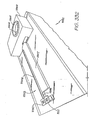
- FIG. 332 an example of an ink jet nozzle arrangement 3301 as constructed in accordance with an embodiment.
- the nozzle arrangement includes a nozzle chamber 3302 normally filled with ink and an actuator mechanism 3303 for actuating a vane 3304 for the ejection of ink from the nozzle chamber 3302 via an ink ejection port 3305.
- Fig. 332 is a perspective view of the ink jet nozzle arrangement of an embodiment in its idle or quiescent in position.
- Fig. 333 illustrates a perspective view after actuation of the actuator 3303.
- the actuator 3303 includes two arms 3306, 3307.
- the two arms can be formed from titanium di-boride (TiB 2 ) which has a high Young's modulus and therefore provides a large degree of bending strength.
- a current is passed along the arms 3306, 3307 with the arm 3307 having a substantially thicker portion along most of its length.
- the arm 3307 is stiff but for in the area of thinned portion 3308 and hence the bending moment is concentrated in the area 3308.
- the thinned arm 3306 is of a thinner form and is heated by means of resistive heating of a current passing through the arms 3306,3307.
- the arms 3306, 3307 are interconnected to electrical circuitry via connections 3310, 3311.
- the arm 3306 Upon heating of the arm 3306, the arm 3306 is expanded with the bending of the arm 3307 being concentrated in the area 3308. This results in movement of the end of the actuator mechanism 3303 which proceeds through a slot in the wall nozzle chamber 3302. The bending further causes movement of vane 3304 so as to increase the pressure of the ink within the nozzle chamber and thereby cause its subsequent ejection from ink ejection nozzle 3305.
- the nozzle chamber 3302 is refilled via an ink channel 3313 ( Fig. 334 ) formed in the wafer substrate 3314. After movement of the vane 3304, so as to cause the ejection of ink, the current to arm 3306 is turned off which results in a corresponding back movement of the end vane 3304.
- the ink within nozzle chamber 3302 is then replenished by means of wafer ink supply channel 3313 which is attached to an ink supply formed on the back of wafer 3314.
- the refill can be by means of a surface tension reduction effects of the ink within nozzle chamber 3302 across ink ejection port 3305.
- Fig. 334 illustrates an exploded perspective view of the components of the ink jet nozzle arrangement.
- an embodiment can be constructed utilising semiconductor processing techniques in addition to micro machining and micro fabrication process technology (MEMS) and a full familiarity with these technologies is hereinafter assumed.
- MEMS micro machining and micro fabrication process technology
- MEMS micro-electro mechanical system
- the nozzles can preferably be constructed by constructing a large array of nozzles on a single silicon wafer at a time.
- the array of nozzles can be divided into multiple print heads, with each print head itself having nozzles grouped into multiple colours to provide for full colour image reproduction.
- the arrangement can be constructed via the utilisation of a standard silicon wafer substrate 33-14 upon which is deposited an electrical circuitry layer 3316 which can comprise a standard CMOS circuitry layer.
- the CMOS layer can include an etched portion defining pit 3317.
- a protective layer (not shown) which comprise silicon nitride or the like.
- a sacrificial material which is initially suitably etched so as to form cavities for the portion of the thermal actuator 3303 and bottom portion of the vane 3304, in addition to the bottom rim of nozzle chamber 3302. These cavities can then be filled with titanium di-boride.
- a similar process is used to form the glass portions of the actuator.
- a further layer of sacrificial material is deposited and suitably etched so as to form the rest of the vane 3304 in addition to a portion of the nozzle chamber walls to the same height of vane 3304.
- a further sacrificial layer is deposited and etched in a suitable manner so as to form the rest of the nozzle chamber 3302.
- the top surface of the nozzle chamber is further etched so as to form the nozzle rim rounding the ejection port 3305.
- the sacrificial material is etched away so as to release the construction of an embodiment. It will be readily evident to those skilled in the art that other MEMS processing steps could be utilized.
- the thermal actuator and vane portions 3303 and 3304 in addition to the nozzle chamber 3305 are constructed from titanium di-boride.
- the utilisation of titanium di-boride is standard in the construction of semiconductor systems and, in addition, its material properties, including a high Young's modulus, is utilised to advantage in the construction of the thermal actuator 3303.
- the actuator 3303 is covered with a hydrophobic material, such as Teflon, so as to prevent any leaking of the liquid out of the slot 3319.
- the ink channel can be etched through the wafer utilising a high anisotropic silicon wafer etchers. This can be done as an anisotropic crystallographic silicon etch, or an anisotropic dry etch.
- a dry etch system capable of high aspect ratio deep silicon trench etching such as the Surface Technology Systems (STS) Advance Silicon Etch (ASE) system is recommended for volume production, as the chip size can be reduced over a wet etch.
- STS Surface Technology Systems
- ASE Advance Silicon Etch
- the wet etch is suitable for small volume production where a suitable plasma etch system is not available. Altema-tively, but undesirably, ink access can be around the sides of the print head chips.
- ink access is through the wafer higher ink flow is possible, and there is less requirement for high accuracy assembly. If ink access is around the edge of the chip, ink flow is severely limited, and the print head chips must be carefully assembled onto ink channel chips. This latter process is difficult due to the possibility of damaging the fragile nozzle plate. If plasma etching is used, the chips can be effectively diced at the same time. Separating the chips by plasma etching allows them to be spaced as little as 35 micron apart, increasing the number of chips on a wafer.
Abstract
Description
- The present invention relates to the field of ink jet printing systems.
- Many different types of printing have been invented, a large number of which are presently in use. The known forms of print have a variety of methods for marking the print media with a relevant marking media. Commonly used forms of printing include offset printing, laser printing and copying devices, dot matrix type impact printers, thermal paper printers, film recorders, thermal wax printers, dye sublimation printers and ink jet printers both of the drop on demand and continuous flow type. Each type of printer has its own advantages and problems when considering cost, speed, quality, reliability, simplicity of construction and operation etc.
- In recent years, the field of ink jet printing, wherein each individual pixel of ink is derived from one or more ink nozzles has become increasingly popular primarily due to its inexpensive and versatile nature.
- Many different techniques of ink jet printing have been invented. For a survey of the field, reference is made to an article by J Moore, "Non-Impact Printing: Introduction and Historical Perspective", Output Hard Copy Devices, Editors R Dubeck and S Sherr, pages 207 - 220 (1988).
- Ink Jet printers themselves come in many different types. The utilisation of a continuous stream ink in ink jet printing appears to date back to at least 1929 wherein
US Patent No. 1941001 by Hansell discloses a simple form of continuous stream electro-static ink jet printing. -
US Patent 3596275 by Sweet also discloses a process of a continuous ink jet printing including the step wherein the ink jet stream is modulated by a high frequency electro-static field so as to cause drop separation. This technique is still utilised by several manufacturers including Elmjet and Scitex (see alsoUS Patent No. 3373437 by Sweet et al ) - Piezo-electric ink jet printers are also one form of commonly utilised ink jet printing device. Piezo-electric systems are disclosed by
Kyser et. al. in US Patent No. 3946398 (1970 ) which utilises a diaphragm mode of operation, byZolten in US Patent 3683272 (1970 ) which discloses a squeeze mode of operation of a piezo electric crystal,Stemme in US Patent No. 3747120 (1972 ) discloses a bend mode of piezo-electric operation,Howkins in US Patent No. 4459601 discloses a Piezo electric push mode actuation of the ink jet stream andFischbeck in US 4584590 which discloses a sheer mode type of piezo-electric transducer element. - Recently, thermal ink jet printing has become an extremely popular form of ink jet printing: The ink jet printing techniques include those disclosed by
Endo et al in GB 2007162 (1979 Vaught et al in US Patent 4490728 . Both the aforementioned references disclosed ink jet printing techniques rely upon the activation of an electrothermal actuator which results in the creation of a bubble in a constricted space, such as a nozzle, which thereby causes the ejection of ink from an aperture connected to the confined space onto a relevant print media. Printing devices utilising the electro-thermal actuator are manufactured by manufacturers such as Canon and Hewlett Packard. -
EP0506232 discloses a valve for a drop on demand ink jet printer employing a lever seal in a housing to control the frequency and quantity of ink delivered to a printing material such as paper. Lever and housing of the chamber are unitary. There is no slit. Ejection is achieved by static pressure. -
WO9418010 - Neither of the documents discloses a movable vane that causes ejection of ink.
- As can be seen from the foregoing, many different types of printing technologies are available. Ideally, a printing technology should have a number of desirable attributes. These include inexpensive construction and operation, high speed operation, safe and continuous long term operation etc. Each technology may have its own advantages and disadvantages in the areas of cost, speed, quality, reliability, power usage, simplicity of construction operation, durability and consumables.
- Many ink jet printing mechanisms are known. Unfortunately, in mass production techniques, the production of ink jet heads is quite difficult. For example, often, the orifice or nozzle plate is constructed separately from the ink supply and ink ejection mechanism and bonded to the mechanism at a later stage (Hewlett-Packard Journal, Vol. 36 no 5, pp33-37 (1985)). These separate material processing steps required in handling such precision devices often adds a substantially expense in manufacturing.
- Additionally, side shooting ink jet technologies (
U.S. Patent No. 4,899,181 ) are often used but again, this limit the amount of mass production throughput given any particular capital investment. - Additionally, more esoteric techniques are also often utilised. These can include electroforming of nickel stage (Hewlett-Packard Journal, Vol. 36 no 5, pp33-37 (1985)), electro-discharge machining, laser ablation (
U.S. Patent No. 5,208,604 ), micro-punching, etc. - The utilisation of the above techniques is likely to add substantial expense to the mass production of ink jet print heads and therefore add substantially to their final cost.
- It would therefore be desirable if an efficient system for the mass production of ink jet print heads could be developed.
- Further, during the construction of micro electromechanical systems, it is common to utilize a sacrificial material to build up a mechanical system, within the sacrificial material being subsequently etched away so as to release the required mechanical structure. For example, a suitable common sacrificial material includes silicon dioxide which can be etched away in hydrofluoric acid. MEMS devices are often constructed on silicon wafers having integral electronics such as, for example, using a multi-level metal CMOS layer. Unfortunately, the CMOS process includes the construction of multiple layers which may include the utilization of materials which can be attacked by the sacrificial etchant. This often necessitates the construction of passivation layers using extra processing steps so as to protect other layers from possible unwanted attack by a sacrificial etchant.
- In micro-electro mechanical system, it is often necessary to provide for the movement of objects. In particular, it is often necessary to pivot objects in addition to providing for fulcrum arrangements where a first movement of one end of the fulcrum is translated into a corresponding measurement of a second end of the fulcrum. Obviously, such arrangements are often fundamental to mechanical apparatuses.
- Further, When constructing large integrated circuits or micro-electro mechanical systems, it is often necessary to interconnect a large number of wire to the final integrated circuit device. To this end, normally, a large number of bond pads are provided on the surface of a chip for the attachment of wires thereto. With the utilization of bond pads normally certain minimal spacings are utilized in accordance with the design technologies utilised. Where are large number of interconnects are required, an excessive amount of on chip real estate is required for providing bond pads. It is therefore desirable to minimize the amount of real estate provided for bond pads whilst ensuring the highest degree of accuracy of registration for automated attachment of interconnects such as a tape automated bonding (TAB) to the surface of a device.
- The present invention relates to ink jet printing and in particular, discloses an ink jet nozzle arrangement in accordance with the claims which follow.
- Notwithstanding any other forms which may fall within the scope of the present invention, preferred forms of the invention will now be described, by way of example only, with reference to the accompanying drawings in which:
-
Fig. 332 illustrates a perspective view of an ink jet nozzle arrangement in accordance with an embodiment; -
Fig. 333 illustrates the arrangement ofFig. 332 when the actuator is in an activated position; -
Fig. 334 illustrates an exploded perspective view of the major components of an embodiment; -
Fig. 335 provides a legend of the materials indicated inFig. 336 to Fig. 347 ; and -
Fig. 336 to Fig. 347 illustrate sectional views of the manufacturing steps in one form of construction of an ink jet printhead nozzle. - In an embodiment, there is provided an ink jet printing system wherein each nozzle has a nozzle chamber having a slotted side wall through which is formed an actuator mechanism attached to a vane within the nozzle chamber such that the actuator can be activated to move the vane within the nozzle chamber to thereby cause ejection of ink from the nozzle chamber.
- Turning now to the figures, there is illustrated in
Fig. 332 an example of an inkjet nozzle arrangement 3301 as constructed in accordance with an embodiment. The nozzle arrangement includes anozzle chamber 3302 normally filled with ink and anactuator mechanism 3303 for actuating avane 3304 for the ejection of ink from thenozzle chamber 3302 via anink ejection port 3305. -
Fig. 332 is a perspective view of the ink jet nozzle arrangement of an embodiment in its idle or quiescent in position.Fig. 333 illustrates a perspective view after actuation of theactuator 3303. - The
actuator 3303 includes twoarms arms arm 3307 having a substantially thicker portion along most of its length. Thearm 3307 is stiff but for in the area of thinnedportion 3308 and hence the bending moment is concentrated in thearea 3308. The thinnedarm 3306 is of a thinner form and is heated by means of resistive heating of a current passing through thearms arms connections - Upon heating of the
arm 3306, thearm 3306 is expanded with the bending of thearm 3307 being concentrated in thearea 3308. This results in movement of the end of theactuator mechanism 3303 which proceeds through a slot in thewall nozzle chamber 3302. The bending further causes movement ofvane 3304 so as to increase the pressure of the ink within the nozzle chamber and thereby cause its subsequent ejection fromink ejection nozzle 3305. Thenozzle chamber 3302 is refilled via an ink channel 3313 (Fig. 334 ) formed in the wafer substrate 3314. After movement of thevane 3304, so as to cause the ejection of ink, the current toarm 3306 is turned off which results in a corresponding back movement of theend vane 3304. The ink withinnozzle chamber 3302 is then replenished by means of wafer ink supply channel 3313 which is attached to an ink supply formed on the back of wafer 3314. The refill can be by means of a surface tension reduction effects of the ink withinnozzle chamber 3302 acrossink ejection port 3305. -
Fig. 334 illustrates an exploded perspective view of the components of the ink jet nozzle arrangement. - Referring now specifically to
Fig. 334 , an embodiment can be constructed utilising semiconductor processing techniques in addition to micro machining and micro fabrication process technology (MEMS) and a full familiarity with these technologies is hereinafter assumed. - For a general introduction to a micro-electro mechanical system (MEMS) reference is made to standard proceedings in this field including the proceeding of the SPIE (International Society for Optical Engineering) including volumes 2642 and 2882 which contain the proceedings of recent advances and conferences in this field.
- The nozzles can preferably be constructed by constructing a large array of nozzles on a single silicon wafer at a time. The array of nozzles can be divided into multiple print heads, with each print head itself having nozzles grouped into multiple colours to provide for full colour image reproduction. The arrangement can be constructed via the utilisation of a standard silicon wafer substrate 33-14 upon which is deposited an electrical circuitry layer 3316 which can comprise a standard CMOS circuitry layer. The CMOS layer can include an etched portion defining pit 3317. On top of the CMOS layer is initially deposited a protective layer (not shown) which comprise silicon nitride or the like. On top of this layer is deposited a sacrificial material which is initially suitably etched so as to form cavities for the portion of the
thermal actuator 3303 and bottom portion of thevane 3304, in addition to the bottom rim ofnozzle chamber 3302. These cavities can then be filled with titanium di-boride. Next, a similar process is used to form the glass portions of the actuator. Next, a further layer of sacrificial material is deposited and suitably etched so as to form the rest of thevane 3304 in addition to a portion of the nozzle chamber walls to the same height ofvane 3304. - Subsequently, a further sacrificial layer is deposited and etched in a suitable manner so as to form the rest of the
nozzle chamber 3302. The top surface of the nozzle chamber is further etched so as to form the nozzle rim rounding theejection port 3305. Subsequently, the sacrificial material is etched away so as to release the construction of an embodiment. It will be readily evident to those skilled in the art that other MEMS processing steps could be utilized. - Preferably, the thermal actuator and
vane portions nozzle chamber 3305 are constructed from titanium di-boride. The utilisation of titanium di-boride is standard in the construction of semiconductor systems and, in addition, its material properties, including a high Young's modulus, is utilised to advantage in the construction of thethermal actuator 3303. - Further, preferably the
actuator 3303 is covered with a hydrophobic material, such as Teflon, so as to prevent any leaking of the liquid out of the slot 3319. - Further, as a final processing step, the ink channel can be etched through the wafer utilising a high anisotropic silicon wafer etchers. This can be done as an anisotropic crystallographic silicon etch, or an anisotropic dry etch. A dry etch system capable of high aspect ratio deep silicon trench etching such as the Surface Technology Systems (STS) Advance Silicon Etch (ASE) system is recommended for volume production, as the chip size can be reduced over a wet etch. The wet etch is suitable for small volume production where a suitable plasma etch system is not available. Altema-tively, but undesirably, ink access can be around the sides of the print head chips. If ink access is through the wafer higher ink flow is possible, and there is less requirement for high accuracy assembly. If ink access is around the edge of the chip, ink flow is severely limited, and the print head chips must be carefully assembled onto ink channel chips. This latter process is difficult due to the possibility of damaging the fragile nozzle plate. If plasma etching is used, the chips can be effectively diced at the same time. Separating the chips by plasma etching allows them to be spaced as little as 35 micron apart, increasing the number of chips on a wafer.
- One form of detailed manufacturing process which can be used to fabricate monolithic ink jet print heads operating in accordance with the principles taught by the present embodiment can proceed utilizing the following steps:
- 1. Using a double sided polished wafer, complete drive transistors, data distribution, and timing circuits using a 0.5 micron, one poly, 2 metal CMOS process. Relevant features of the wafer at this step are shown in
Fig. 336 . For clarity, these diagrams may not be to scale, and may not represent a cross section though any single plane of the nozzle.Fig. 335 is a key to representations of various materials in these manufacturing diagrams, and those of other cross referenced ink jet configurations. - 2. Etch oxide down to silicon or aluminum using Mask 1. This mask defines the ink inlet, the heater contact vias, and the edges of the print head chips. This step is shown in
Fig. 337 . - 3. Deposit 1 micron of sacrificial material (e.g. aluminum)
- 4. Etch the sacrificial layer using Mask 2, defining the nozzle chamber wall and the actuator anchor point. This step is shown in
Fig. 338 . - 5. Deposit 1 micron of heater material, for example titanium nitride (TiN) or titanium diboride (TiB2).
- 6. Etch the heater material using Mask 3, which defines the actuator loop and the lowest layer of the nozzle wall. This step is shown in
Fig. 339 . - 7. Wafer probe. All electrical connections are complete at this point, bond pads are accessible, and the chips are not yet separated.
- 8. Deposit 1 micron of titanium nitride.
- 9. Etch the titanium
nitride using Mask 4, which defines the nozzle chamber wall, with the exception of the nozzle chamber actuator slot, and the paddle. This step is shown inFig. 340 . - 10. Deposit 8 microns of sacrificial material.
- 11. Etch the sacrificial material down to titanium nitride using Mask 5. This mask defines the nozzle chamber wall and the paddle. This step is shown in
Fig. 341 . - 12. Deposit a 0.5 micron conformal layer of titanium nitride and planarize down to the sacrificial layer using CMP.
- 13. Deposit 1 micron of sacrificial material.
- 14. Etch the sacrificial material down to titanium nitride using Mask 6. This mask defines the nozzle chamber wall. This step is shown in
Fig. 342 . - 15. Deposit 1 microns of titanium nitride.
- 16. Etch to a depth of (approx.) 0.5 micron using Mask 7. This mask defines the nozzle rim. This step is shown in
Fig. 343 . - 17. Etch down to the sacrificial layer using Mask 8. This mask defines the roof of the nozzle chamber, and the nozzle itself. This step is shown in
Fig. 344 . - 18. Back-etch completely through the silicon wafer (with, for example, an ASE Advanced Silicon Etcher from Surface Technology Systems) using Mask 9. This mask defines the ink inlets which are etched through the wafer. The wafer is also diced by this etch. This step is shown in
Fig. 345 . - 19. Etch the sacrificial material. The nozzle chambers are cleared, the actuators freed, and the chips are separated by this etch. This step is shown in
Fig. 346 . - 20. Mount the print heads in their packaging, which may be a molded plastic former incorporating ink channels which supply the appropriate color ink to the ink inlets at the back of the wafer.
- 21. Connect the print heads to their interconnect systems. For a low profile connection with minimum disruption of airflow, TAB may be used. Wire bonding may also be used if the printer is to be operated with sufficient clearance to the paper.
- 22. Hydrophobize the front surface of the print heads.
- 23. Fill the completed print heads with ink and test them. A filled nozzle is shown in
Fig. 347 .
Claims (10)
- An ink jet nozzle arrangement comprising:a nozzle chamber (3302) having a slotted sidewall in a first surface and an ink ejection port (3305) defined in a second surface thereof;an ink supply channel interconnected to said nozzle chamber for the supply of ink to said nozzle chamber;a moveable vane (3304) located within said nozzle chamber and being moveable so as to cause the ejection of ink from said nozzle chamber; andan actuator located (3303) outside said nozzle chamber and interconnected to said moveable vane through said slotted sidewall.
- An ink jet nozzle as claimed in claim 1 wherein said moveable vane, in its quiescent position, is located substantially adjacent a first end of said slot and said actuator is actuated to move said moveable vane from said first end of said slot to a second end of said slot.
- An inkjet nozzle arrangement as claimed in claim 1 or 2 wherein said actuator comprises a thermal actuator which is actuated by means of an electric current passed through the thermal actuator resulting in resistive heating of said actuator.
- An ink jet nozzle arrangement as claimed in claim 3 wherein said thermal actuator is constructed of a conductive material having a high Young's modulus.
- An ink jet nozzle arrangement as claimed in claim 3 wherein said thermal actuator includes a first (3306) and second arm (3307), said first arm undergoing resistive heating to thereby cause said first arm to bend resulting in actuation by said thermal actuator.
- An ink jet nozzle arrangement as claimed in claim 5 wherein the first arm has a thinned cross-section relative to the second arm,
- An ink jet nozzle arrangement as claimed in claim 5 wherein said arms are attached to a substrate at one end.
- An ink jet nozzle arrangement as claimed in any one of the preceding claims wherein said actuator device operates in an ambient atmosphere.
- An ink jet nozzle arrangement as claimed in any of the preceding claims wherein the portions of said actuator located adjacent the exterior of said slotted side wall are coated with a hydrophobic material.
- An ink jet nozzle arrangement as claimed in any of the preceding claims wherein said arrangement is formed on a silicon wafer and said ink supply channel is formed by etching a channel through said silicon wafer.
Applications Claiming Priority (72)
| Application Number | Priority Date | Filing Date | Title |
|---|---|---|---|
| AUPO7933A AUPO793397A0 (en) | 1997-07-15 | 1997-07-15 | A method of manufacture of an image creation_apparatus (IJM10) |
| AUPO8038A AUPO803897A0 (en) | 1997-07-15 | 1997-07-15 | Image creation method and apparatus (IJ18) |
| AUPO8001A AUPO800197A0 (en) | 1997-07-15 | 1997-07-15 | Image creation method and apparatus (IJ17) |
| AUPO8046A AUPO804697A0 (en) | 1997-07-15 | 1997-07-15 | A method of manufacture of an image creation apparatus (IJM30) |
| AUPO7945A AUPO794597A0 (en) | 1997-07-15 | 1997-07-15 | A device (MEMS08) |
| AUPO7951A AUPO795197A0 (en) | 1997-07-15 | 1997-07-15 | A method of manufacture of an image creation apparatus (IJM22) |
| AUPO8034A AUPO803497A0 (en) | 1997-07-15 | 1997-07-15 | Image creation method and apparatus (IJ23) |
| AUPO7937A AUPO793797A0 (en) | 1997-07-15 | 1997-07-15 | A method of manufacture of an image creation apparatus (IJM03) |
| AUPO7952A AUPO795297A0 (en) | 1997-07-15 | 1997-07-15 | A method of manufacture of an image creation apparatus (IJM29) |
| AUPO8007A AUPO800797A0 (en) | 1997-07-15 | 1997-07-15 | A device (MEMS03) |
| AUPO8043A AUPO804397A0 (en) | 1997-07-15 | 1997-07-15 | Image creation method and apparatus (IJ28) |
| AUPO7941A AUPO794197A0 (en) | 1997-07-15 | 1997-07-15 | A method of manufacture of an image creation apparatus (IJM24) |
| AUPO8079A AUPO807997A0 (en) | 1997-07-15 | 1997-07-15 | A method of manufacture of an image creation apparatus (IJM18) |
| AUPO8074A AUPO807497A0 (en) | 1997-07-15 | 1997-07-15 | A method of manufacture of an image creation apparatus (IJM23) |
| AUPO8051A AUPO805197A0 (en) | 1997-07-15 | 1997-07-15 | A method of manufacture of an image creation apparatus (IJM27) |
| AUPO7946A AUPO794697A0 (en) | 1997-07-15 | 1997-07-15 | A device (MEMS10) |
| AUPO7947A AUPO794797A0 (en) | 1997-07-15 | 1997-07-15 | A device (MEMS07) |
| AUPO8064A AUPO806497A0 (en) | 1997-07-15 | 1997-07-15 | Image creation method and apparatus (IJ30) |
| AUPO8050A AUPO805097A0 (en) | 1997-07-15 | 1997-07-15 | A method of manufacture of an image creation apparatus (IJM19) |
| AUPO8042A AUPO804297A0 (en) | 1997-07-15 | 1997-07-15 | Image creation method and apparatus (IJ29) |
| AUPO8002A AUPO800297A0 (en) | 1997-07-15 | 1997-07-15 | Image creation method and apparatus (IJ20) |
| AUPO8033A AUPO803397A0 (en) | 1997-07-15 | 1997-07-15 | Image creation method and apparatus (IJ19) |
| AUPO7943A AUPO794397A0 (en) | 1997-07-15 | 1997-07-15 | A device (MEMS01) |
| AUPO8006A AUPO800697A0 (en) | 1997-07-15 | 1997-07-15 | A device (MEMS02) |
| AUPO8052A AUPO805297A0 (en) | 1997-07-15 | 1997-07-15 | A method of manufacture of an image creation apparatus (IJM20) |
| AUPO8075A AUPO807597A0 (en) | 1997-07-15 | 1997-07-15 | A method of manufacture of an image creation apparatus (IJM17) |
| AUPO8057A AUPO805797A0 (en) | 1997-07-15 | 1997-07-15 | Image creation method and apparatus (IJ09) |
| AUPO8010A AUPO801097A0 (en) | 1997-07-15 | 1997-07-15 | A device (MEMS05) |
| AUPO8040A AUPO804097A0 (en) | 1997-07-15 | 1997-07-15 | Image creation method and apparatus (IJ03) |
| AUPO8056A AUPO805697A0 (en) | 1997-07-15 | 1997-07-15 | Image creation method and apparatus (IJ10) |
| AUPO7948A AUPO794897A0 (en) | 1997-07-15 | 1997-07-15 | A method of manufacture of an image creation apparatus (IJM21) |
| AUPO8011A AUPO801197A0 (en) | 1997-07-15 | 1997-07-15 | A device (MEMS06) |
| AUPO8068A AUPO806897A0 (en) | 1997-07-15 | 1997-07-15 | Image creation method and apparatus (IJ21) |
| AUPO8045A AUPO804597A0 (en) | 1997-07-15 | 1997-07-15 | A method of manufacture of an image creation apparatus (IJM28) |
| AUPO8078A AUPO807897A0 (en) | 1997-07-15 | 1997-07-15 | A method of manufacture of an image creation apparatus (IJM09) |
| AUPO8008A AUPO800897A0 (en) | 1997-07-15 | 1997-07-15 | A device (MEMS04) |
| AUPO8037A AUPO803797A0 (en) | 1997-07-15 | 1997-07-15 | Image creation method and apparatus (IJ27) |
| AUPO8039A AUPO803997A0 (en) | 1997-07-15 | 1997-07-15 | Image creation method and apparatus (IJ24) |
| AUPO7944A AUPO794497A0 (en) | 1997-07-15 | 1997-07-15 | A device (MEMS09) |
| AUPO8062A AUPO806297A0 (en) | 1997-07-15 | 1997-07-15 | Image creation method and apparatus (IJ22) |
| AUPO8503A AUPO850397A0 (en) | 1997-08-11 | 1997-08-11 | A method of manufacture of an image creation apparatus (ijm30a) |
| AUPO9390A AUPO939097A0 (en) | 1997-09-23 | 1997-09-23 | A method of manufacture of an image creation apparatus (IJM31) |
| AUPO9392A AUPO939297A0 (en) | 1997-09-23 | 1997-09-23 | A method of manufacture of an image creation apparatus (IJM32) |
| AUPO9391A AUPO939197A0 (en) | 1997-09-23 | 1997-09-23 | Image creation method and apparatus (IJ32) |
| AUPO9393A AUPO939397A0 (en) | 1997-09-23 | 1997-09-23 | A device and method (MEMS11) |
| AUPO9389A AUPO938997A0 (en) | 1997-09-23 | 1997-09-23 | Image creation method and apparatus (IJ31) |
| AUPP0875A AUPP087597A0 (en) | 1997-12-12 | 1997-12-12 | A device (MEMS12) |
| AUPP0891A AUPP089197A0 (en) | 1997-12-12 | 1997-12-12 | Image creation method and apparatus (IJ34) |
| AUPP0894A AUPP089497A0 (en) | 1997-12-12 | 1997-12-12 | An interconnection system (MEMS13) |
| AUPP0882A AUPP088297A0 (en) | 1997-12-12 | 1997-12-12 | A method of manufacture of an image creation apparatus (IJM37) |
| AUPP0893A AUPP089397A0 (en) | 1997-12-12 | 1997-12-12 | Image creation method and apparatus (IJ37) |
| AUPP0874A AUPP087497A0 (en) | 1997-12-12 | 1997-12-12 | A method of manufacture of an image creation apparatus (IJM38) |
| AUPP0888A AUPP088897A0 (en) | 1997-12-12 | 1997-12-12 | Image creation method and apparatus (IJ33) |
| AUPP0889A AUPP088997A0 (en) | 1997-12-12 | 1997-12-12 | A method of manufacture of an image creation apparatus (IJM35) |
| AUPP0873A AUPP087397A0 (en) | 1997-12-12 | 1997-12-12 | Image creation method and apparatus (IJ36) |
| AUPP0890A AUPP089097A0 (en) | 1997-12-12 | 1997-12-12 | Image creation method and apparatus (IJ35) |
| AUPP0892A AUPP089297A0 (en) | 1997-12-12 | 1997-12-12 | Image creation method and apparatus (IJ38) |
| AUPP0872A AUPP087297A0 (en) | 1997-12-12 | 1997-12-12 | Image creation method and apparatus (IJM36) |
| AUPP1396A AUPP139698A0 (en) | 1998-01-19 | 1998-01-19 | A method of manufacture of an image creation apparatus (ijm39) |
| AUPP1398A AUPP139898A0 (en) | 1998-01-19 | 1998-01-19 | An image creation method and apparatus (ij39) |
| AUPP2592A AUPP259298A0 (en) | 1998-03-25 | 1998-03-25 | Image creation method and apparatus (IJ40) |
| AUPP2591A AUPP259198A0 (en) | 1998-03-25 | 1998-03-25 | Image creation method and apparatus (IJM41) |
| AUPP2593A AUPP259398A0 (en) | 1998-03-25 | 1998-03-25 | Image creation method and apparatus (IJ41) |
| AUPP3987A AUPP398798A0 (en) | 1998-06-09 | 1998-06-09 | Image creation method and apparatus (ij43) |
| AUPP3991A AUPP399198A0 (en) | 1998-06-09 | 1998-06-09 | Image creation method and apparatus (ij42) |
| AUPP3989A AUPP398998A0 (en) | 1998-06-09 | 1998-06-09 | A method of manufacture of an image creation apparatus (ijm40) |
| AUPP3990A AUPP399098A0 (en) | 1998-06-09 | 1998-06-09 | A method of manufacture of image creation apparatus (ijm42) |
| AUPP3984A AUPP398498A0 (en) | 1998-06-09 | 1998-06-09 | A method of manufacture of an image creation apparatus (ijm44) |
| AUPP3985A AUPP398598A0 (en) | 1998-06-09 | 1998-06-09 | Image creation method and apparatus (ij44) |
| AUPP3986A AUPP398698A0 (en) | 1998-06-09 | 1998-06-09 | A method of manufacture of an image creation apparatus (ijm43) |
| AUPP3983A AUPP398398A0 (en) | 1998-06-09 | 1998-06-09 | Image creation method and apparatus (ij45) |
| EP98933352A EP0999934B1 (en) | 1997-07-15 | 1998-07-15 | A thermally actuated ink jet |
Related Parent Applications (1)
| Application Number | Title | Priority Date | Filing Date |
|---|---|---|---|
| EP98933352A Division EP0999934B1 (en) | 1997-07-15 | 1998-07-15 | A thermally actuated ink jet |
Publications (2)
| Publication Number | Publication Date |
|---|---|
| EP1650031A1 EP1650031A1 (en) | 2006-04-26 |
| EP1650031B1 true EP1650031B1 (en) | 2008-02-20 |
Family
ID=27587066
Family Applications (5)
| Application Number | Title | Priority Date | Filing Date |
|---|---|---|---|
| EP05109701A Expired - Lifetime EP1640162B1 (en) | 1997-07-15 | 1998-07-15 | Inkjet nozzle arrangement having paddle forming a portion of a wall |
| EP98933352A Expired - Lifetime EP0999934B1 (en) | 1997-07-15 | 1998-07-15 | A thermally actuated ink jet |
| EP05109707A Expired - Lifetime EP1650030B1 (en) | 1997-07-15 | 1998-07-15 | Nozzle chamber with paddle vane and externally located thermal actuator |
| EP05109756A Expired - Lifetime EP1650031B1 (en) | 1997-07-15 | 1998-07-15 | Ink jet nozzle with slotted sidewall and moveable vane |
| EP05109700A Expired - Lifetime EP1637330B1 (en) | 1997-07-15 | 1998-07-15 | Thermal actuator with corrugated heater element |
Family Applications Before (3)
| Application Number | Title | Priority Date | Filing Date |
|---|---|---|---|
| EP05109701A Expired - Lifetime EP1640162B1 (en) | 1997-07-15 | 1998-07-15 | Inkjet nozzle arrangement having paddle forming a portion of a wall |
| EP98933352A Expired - Lifetime EP0999934B1 (en) | 1997-07-15 | 1998-07-15 | A thermally actuated ink jet |
| EP05109707A Expired - Lifetime EP1650030B1 (en) | 1997-07-15 | 1998-07-15 | Nozzle chamber with paddle vane and externally located thermal actuator |
Family Applications After (1)
| Application Number | Title | Priority Date | Filing Date |
|---|---|---|---|
| EP05109700A Expired - Lifetime EP1637330B1 (en) | 1997-07-15 | 1998-07-15 | Thermal actuator with corrugated heater element |
Country Status (5)
| Country | Link |
|---|---|
| EP (5) | EP1640162B1 (en) |
| JP (1) | JP4160250B2 (en) |
| AT (4) | ATE359915T1 (en) |
| ES (1) | ES2302134T3 (en) |
| WO (1) | WO1999003681A1 (en) |
Families Citing this family (90)
| Publication number | Priority date | Publication date | Assignee | Title |
|---|---|---|---|---|
| US7334874B2 (en) * | 1997-07-15 | 2008-02-26 | Silverbrook Research Pty Ltd | Inkjet nozzle chamber with electrostatically attracted plates |
| US7527357B2 (en) | 1997-07-15 | 2009-05-05 | Silverbrook Research Pty Ltd | Inkjet nozzle array with individual feed channel for each nozzle |
| US7410243B2 (en) | 1997-07-15 | 2008-08-12 | Silverbrook Research Pty Ltd | Inkjet nozzle with resiliently biased ejection actuator |
| US6935724B2 (en) | 1997-07-15 | 2005-08-30 | Silverbrook Research Pty Ltd | Ink jet nozzle having actuator with anchor positioned between nozzle chamber and actuator connection point |
| US7556356B1 (en) | 1997-07-15 | 2009-07-07 | Silverbrook Research Pty Ltd | Inkjet printhead integrated circuit with ink spread prevention |
| US7234795B2 (en) * | 1997-07-15 | 2007-06-26 | Silverbrook Research Pty Ltd | Inkjet nozzle with CMOS compatible actuator voltage |
| US7753491B2 (en) | 1997-07-15 | 2010-07-13 | Silverbrook Research Pty Ltd | Printhead nozzle arrangement incorporating a corrugated electrode |
| US7195339B2 (en) | 1997-07-15 | 2007-03-27 | Silverbrook Research Pty Ltd | Ink jet nozzle assembly with a thermal bend actuator |
| US7328975B2 (en) * | 1997-07-15 | 2008-02-12 | Silverbrook Research Pty Ltd | Injet printhead with thermal bend arm exposed to ink flow |
| US7207654B2 (en) | 1997-07-15 | 2007-04-24 | Silverbrook Research Pty Ltd | Ink jet with narrow chamber |
| US7468139B2 (en) | 1997-07-15 | 2008-12-23 | Silverbrook Research Pty Ltd | Method of depositing heater material over a photoresist scaffold |
| US7465030B2 (en) | 1997-07-15 | 2008-12-16 | Silverbrook Research Pty Ltd | Nozzle arrangement with a magnetic field generator |
| US20040130599A1 (en) * | 1997-07-15 | 2004-07-08 | Silverbrook Research Pty Ltd | Ink jet printhead with amorphous ceramic chamber |
| US7337532B2 (en) | 1997-07-15 | 2008-03-04 | Silverbrook Research Pty Ltd | Method of manufacturing micro-electromechanical device having motion-transmitting structure |
| US6682174B2 (en) | 1998-03-25 | 2004-01-27 | Silverbrook Research Pty Ltd | Ink jet nozzle arrangement configuration |
| US6712453B2 (en) | 1997-07-15 | 2004-03-30 | Silverbrook Research Pty Ltd. | Ink jet nozzle rim |
| AUPP654598A0 (en) | 1998-10-16 | 1998-11-05 | Silverbrook Research Pty Ltd | Micromechanical device and method (ij46h) |
| US7360871B2 (en) * | 1997-07-15 | 2008-04-22 | Silverbrook Research Pty Ltd | Inkjet chamber with ejection actuator between inlet and nozzle |
| US6648453B2 (en) | 1997-07-15 | 2003-11-18 | Silverbrook Research Pty Ltd | Ink jet printhead chip with predetermined micro-electromechanical systems height |
| US6488361B2 (en) * | 1997-07-15 | 2002-12-03 | Silverbrook Research Pty Ltd. | Inkjet printhead that incorporates closure mechanisms |
| US6855264B1 (en) | 1997-07-15 | 2005-02-15 | Kia Silverbrook | Method of manufacture of an ink jet printer having a thermal actuator comprising an external coil spring |
| US6435667B1 (en) * | 1997-12-12 | 2002-08-20 | Silverbrook Research Pty Ltd. | Opposed ejection ports and ink inlets in an ink jet printhead chip |
| US6805435B2 (en) * | 1998-10-16 | 2004-10-19 | Silverbrook Research Pty Ltd | Printhead assembly with an ink distribution arrangement |
| US6623108B2 (en) * | 1998-10-16 | 2003-09-23 | Silverbrook Research Pty Ltd | Ink jet printhead having thermal bend actuator heating element electrically isolated from nozzle chamber ink |
| WO2000023279A1 (en) | 1998-10-16 | 2000-04-27 | Silverbrook Research Pty. Limited | Improvements relating to inkjet printers |
| US6984023B2 (en) | 1999-02-15 | 2006-01-10 | Silverbrook Research Pty Ltd | Micro-electromechanical displacement device |
| AUPP868699A0 (en) | 1999-02-15 | 1999-03-11 | Silverbrook Research Pty Ltd | A method and apparatus(IJ46P1A) |
| US6860107B2 (en) | 1999-02-15 | 2005-03-01 | Silverbrook Research Pty Ltd | Integrated circuit device having electrothermal actuators |
| ATE344214T1 (en) * | 1999-02-15 | 2006-11-15 | Silverbrook Res Pty Ltd | THERMAL BENDING ACTUATOR AND BLADE STRUCTURE FOR INKJET NOZZLE |
| US6792754B2 (en) | 1999-02-15 | 2004-09-21 | Silverbrook Research Pty Ltd | Integrated circuit device for fluid ejection |
| AU775594B2 (en) * | 1999-03-16 | 2004-08-05 | Silverbrook Research Pty. Ltd. | A method of manufacturing a thermal bend actuator |
| AUPP922399A0 (en) | 1999-03-16 | 1999-04-15 | Silverbrook Research Pty Ltd | A method and apparatus (ij46p2) |
| AU769819B2 (en) * | 1999-04-22 | 2004-02-05 | Memjet Technology Limited | Thermal actuator shaped for more uniform temperature profile |
| AUPP993199A0 (en) * | 1999-04-22 | 1999-05-20 | Silverbrook Research Pty Ltd | A micromechanical device and method (ij46p2a) |
| AU2004202252B2 (en) * | 1999-04-22 | 2005-06-30 | Silverbrook Research Pty Ltd | Liquid ejection using a micro-electromechanical device |
| AU2004201743B2 (en) * | 1999-04-22 | 2005-05-19 | Silverbrook Research Pty Ltd | Thermal actuator with heat sinks |
| AU770756B2 (en) * | 1999-04-22 | 2004-03-04 | Memjet Technology Limited | Actuator control in a micro electro-mechanical liquid ejection device |
| AUPP993099A0 (en) * | 1999-04-22 | 1999-05-20 | Silverbrook Research Pty Ltd | A micromechancial device and method(ij46p2b) |
| AUPQ130899A0 (en) * | 1999-06-30 | 1999-07-22 | Silverbrook Research Pty Ltd | A method and apparatus (IJ47V12) |
| AU761821B2 (en) * | 1999-06-30 | 2003-06-12 | Silverbrook Research Pty Ltd | Fault detection in a micro electro-mechanical device |
| AUPQ131099A0 (en) * | 1999-06-30 | 1999-07-22 | Silverbrook Research Pty Ltd | A method and apparatus (IJ47V8) |
| AUPQ130999A0 (en) * | 1999-06-30 | 1999-07-22 | Silverbrook Research Pty Ltd | A method and apparatus (IJ47V11) |
| US6382779B1 (en) | 1999-06-30 | 2002-05-07 | Silverbrook Research Pty Ltd | Testing a micro electro- mechanical device |
| AU761820B2 (en) * | 1999-06-30 | 2003-06-12 | Silverbrook Research Pty Ltd | Calibrating a micro electro-mechanical device |
| EP1206351B1 (en) * | 1999-06-30 | 2008-07-09 | Silverbrook Research Pty. Limited | Testing a micro electro-mechanical device |
| AUPQ130799A0 (en) * | 1999-06-30 | 1999-07-22 | Silverbrook Research Pty Ltd | A method and apparatus (IJ47V13) |
| AU761670B2 (en) * | 1999-06-30 | 2003-06-05 | Silverbrook Research Pty Ltd | Testing a micro electro-mechanical device |
| SG121872A1 (en) | 1999-09-17 | 2006-05-26 | Silverbrook Res Pty Ltd | Method and system for instruction of a computer using processing sensor |
| AUPQ595700A0 (en) | 2000-03-02 | 2000-03-23 | Silverbrook Research Pty Ltd | Alignment module for printheads |
| US6439693B1 (en) * | 2000-05-04 | 2002-08-27 | Silverbrook Research Pty Ltd. | Thermal bend actuator |
| US6557970B2 (en) | 2000-05-23 | 2003-05-06 | Silverbrook Research Pty Ltd | Nozzle guard for a printhead |
| US6428133B1 (en) | 2000-05-23 | 2002-08-06 | Silverbrook Research Pty Ltd. | Ink jet printhead having a moving nozzle with an externally arranged actuator |
| US6526658B1 (en) | 2000-05-23 | 2003-03-04 | Silverbrook Research Pty Ltd | Method of manufacture of an ink jet printhead having a moving nozzle with an externally arranged actuator |
| US6921153B2 (en) | 2000-05-23 | 2005-07-26 | Silverbrook Research Pty Ltd | Liquid displacement assembly including a fluidic sealing structure |
| US6412904B1 (en) * | 2000-05-23 | 2002-07-02 | Silverbrook Research Pty Ltd. | Residue removal from nozzle guard for ink jet printhead |
| ATE367266T1 (en) * | 2000-05-24 | 2007-08-15 | Silverbrook Res Pty Ltd | MANUFACTURING METHOD FOR A MOVING NOZZLE INK JET PRINT HEAD AND EXTERNAL ACTUATOR |
| US7237873B2 (en) | 2002-11-23 | 2007-07-03 | Silverbrook Research Pty Ltd | Inkjet printhead having low pressure ink ejection zone |
| DE60040622D1 (en) | 2000-05-24 | 2008-12-04 | Silverbrook Res Pty Ltd | FLUIDIC SEAL FOR INK JET ASSEMBLY |
| ATE362847T1 (en) | 2000-05-24 | 2007-06-15 | Silverbrook Res Pty Ltd | INKJET PRINT HEAD WITH MOVING NOZZLE AND EXTERNAL ACTUATOR |
| CN100417523C (en) * | 2000-05-24 | 2008-09-10 | 西尔弗布鲁克研究有限公司 | Ink-jet printing head with isolated nozzle controller |
| US6364460B1 (en) | 2000-06-13 | 2002-04-02 | Chad R. Sager | Liquid delivery system |
| AU2006225215B2 (en) * | 2000-06-30 | 2009-04-09 | Zamtec Limited | An ink ejector for an inkjet printer with an arm and paddle arrangement |
| EP1301346B1 (en) * | 2000-06-30 | 2007-08-15 | Silverbrook Research Pty. Limited | Buckle resistant thermal bend actuators |
| CN100335278C (en) * | 2000-06-30 | 2007-09-05 | 西尔弗布鲁克研究有限公司 | Buckle resistant thermal bend actuators |
| US7095309B1 (en) | 2000-10-20 | 2006-08-22 | Silverbrook Research Pty Ltd | Thermoelastic actuator design |
| US6402301B1 (en) * | 2000-10-27 | 2002-06-11 | Lexmark International, Inc | Ink jet printheads and methods therefor |
| US6561627B2 (en) | 2000-11-30 | 2003-05-13 | Eastman Kodak Company | Thermal actuator |
| AUPR292301A0 (en) * | 2001-02-06 | 2001-03-01 | Silverbrook Research Pty. Ltd. | A method and apparatus (ART99) |
| GB2375185A (en) * | 2001-05-04 | 2002-11-06 | Kymata Ltd | Thick wafer for MEMS fabrication |
| JP2003025564A (en) * | 2001-07-11 | 2003-01-29 | Matsushita Electric Ind Co Ltd | Ink jet head |
| US7160806B2 (en) * | 2001-08-16 | 2007-01-09 | Hewlett-Packard Development Company, L.P. | Thermal inkjet printhead processing with silicon etching |
| US6536874B1 (en) | 2002-04-12 | 2003-03-25 | Silverbrook Research Pty Ltd | Symmetrically actuated ink ejection components for an ink jet printhead chip |
| US7364269B2 (en) | 2002-04-12 | 2008-04-29 | Silverbrook Research Pty Ltd | Inkjet printhead with non-uniform width ink supply passage to nozzle |
| US6857728B2 (en) | 2002-12-02 | 2005-02-22 | Silverbrook Research Pty Ltd | Pagewidth printhead chip having symmetrically actuated fluid ejection components |
| US7575298B2 (en) | 2002-04-12 | 2009-08-18 | Silverbrook Research Pty Ltd | Inkjet printhead with ink supply passage to nozzle etched from opposing sides of wafer |
| US6885083B2 (en) | 2002-10-31 | 2005-04-26 | Hewlett-Packard Development Company, L.P. | Drop generator die processing |
| US8091984B2 (en) | 2002-12-02 | 2012-01-10 | Silverbrook Research Pty Ltd | Inkjet printhead employing active and static ink ejection structures |
| US7377620B2 (en) | 2005-05-26 | 2008-05-27 | Hewlett-Packard Development Company, L.P. | Hydrophobic nozzle exit with improved micro fluid ejection dynamics |
| JP2008012911A (en) * | 2006-06-07 | 2008-01-24 | Canon Inc | Liquid ejection head and its manufacturing method |
| JP4933629B2 (en) * | 2006-12-04 | 2012-05-16 | シルバーブルック リサーチ ピーティワイ リミテッド | Inkjet nozzle assembly having a thermal bending actuator that defines the main part of the nozzle chamber roof with an active beam |
| CN102202895B (en) | 2008-10-31 | 2014-06-25 | 惠普开发有限公司 | Electrostatic liquid-ejection actuation mechanism and electrostatic liquid-ejection device |
| US8152337B2 (en) * | 2009-05-01 | 2012-04-10 | Billboard Video, Inc. | Electronic display panel |
| US8079668B2 (en) | 2009-08-25 | 2011-12-20 | Silverbrook Research Pty Ltd | Crack-resistant thermal bend actuator |
| US8281482B2 (en) | 2009-08-25 | 2012-10-09 | Zamtec Limited | Method of fabricating crack-resistant thermal bend actuator |
| SG178479A1 (en) * | 2009-08-25 | 2012-04-27 | Silverbrook Res Pty Ltd | Crack-resistant thermal bend actuator |
| US8444255B2 (en) | 2011-05-18 | 2013-05-21 | Hewlett-Packard Development Company, L.P. | Power distribution in a thermal ink jet printhead |
| US10537913B2 (en) | 2013-04-29 | 2020-01-21 | Hewlett-Packard Development Company, L.P. | Selective slot coating |
| CN106362899B (en) * | 2016-11-16 | 2018-10-30 | 吉林大学 | A kind of imitative cilium formula high-precision nanodrop ejecting device |
| CN110970252A (en) * | 2019-12-25 | 2020-04-07 | 深圳市博微恩科技有限公司 | Keyboard bottom plate structure and bottom plate color covering area manufacturing method |
| CN111498983A (en) * | 2020-04-22 | 2020-08-07 | 图方便(苏州)环保科技有限公司 | Filter device for sewage treatment based on MBBR and treatment method |
Family Cites Families (73)
| Publication number | Priority date | Publication date | Assignee | Title |
|---|---|---|---|---|
| US1941001A (en) | 1929-01-19 | 1933-12-26 | Rca Corp | Recorder |
| GB792145A (en) * | 1953-05-20 | 1958-03-19 | Technograph Printed Circuits L | Improvements in and relating to devices for obtaining a mechanical movement from theaction of an electric current |
| US3596275A (en) | 1964-03-25 | 1971-07-27 | Richard G Sweet | Fluid droplet recorder |
| US3373437A (en) | 1964-03-25 | 1968-03-12 | Richard G. Sweet | Fluid droplet recorder with a plurality of jets |
| DE1648322A1 (en) * | 1967-07-20 | 1971-03-25 | Vdo Schindling | Measuring or switching element made of bimetal |
| US3946398A (en) | 1970-06-29 | 1976-03-23 | Silonics, Inc. | Method and apparatus for recording with writing fluids and drop projection means therefor |
| US3683212A (en) | 1970-09-09 | 1972-08-08 | Clevite Corp | Pulsed droplet ejecting system |
| SE349676B (en) | 1971-01-11 | 1972-10-02 | N Stemme | |
| FR2188389B1 (en) * | 1972-06-08 | 1975-06-13 | Cibie Projecteurs | |
| FR2231076A2 (en) * | 1973-05-24 | 1974-12-20 | Electricite De France | Driving organ operated by thermal means - esp. for use in corrosive or dangerous environments formed by two metal strips |
| CA1127227A (en) | 1977-10-03 | 1982-07-06 | Ichiro Endo | Liquid jet recording process and apparatus therefor |
| DE2905063A1 (en) * | 1979-02-10 | 1980-08-14 | Olympia Werke Ag | Ink nozzle air intake avoidance system - has vibratory pressure generator shutting bore in membrane in rest position |
| US4459601A (en) | 1981-01-30 | 1984-07-10 | Exxon Research And Engineering Co. | Ink jet method and apparatus |
| US4490728A (en) | 1981-08-14 | 1984-12-25 | Hewlett-Packard Company | Thermal ink jet printer |
| JPS58112747A (en) * | 1981-12-26 | 1983-07-05 | Fujitsu Ltd | Ink jet recording device |
| JPS58116165A (en) * | 1981-12-29 | 1983-07-11 | Canon Inc | Ink injection head |
| DE3214791A1 (en) * | 1982-04-21 | 1983-10-27 | Siemens AG, 1000 Berlin und 8000 München | WRITING DEVICE WORKING WITH LIQUID DROPS |
| DE3378966D1 (en) | 1982-05-28 | 1989-02-23 | Xerox Corp | Pressure pulse droplet ejector and array |
| US4423401A (en) * | 1982-07-21 | 1983-12-27 | Tektronix, Inc. | Thin-film electrothermal device |
| DE3245283A1 (en) * | 1982-12-07 | 1984-06-07 | Siemens AG, 1000 Berlin und 8000 München | Arrangement for expelling liquid droplets |
| US4553393A (en) * | 1983-08-26 | 1985-11-19 | The United States Of America As Represented By The Administrator Of The National Aeronautics And Space Administration | Memory metal actuator |
| JPS6125849A (en) * | 1984-07-17 | 1986-02-04 | Canon Inc | Ink jet recording device |
| DE3430155A1 (en) * | 1984-08-16 | 1986-02-27 | Siemens AG, 1000 Berlin und 8000 München | Indirectly heated bimetal |
| JPS61106259A (en) * | 1984-10-31 | 1986-05-24 | Hitachi Ltd | Ink droplet jet discharging device |
| SE447222B (en) * | 1984-12-21 | 1986-11-03 | Swedot System Ab | ELECTROMAGNETIC MANOVERABLE VALVE DEVICE, SPECIFICALLY FOR GENERATING DROPS IN A HYDRAULIC PRINTER |
| JPS61268453A (en) * | 1985-05-23 | 1986-11-27 | Olympus Optical Co Ltd | Ink jet printer head |
| US5258774A (en) * | 1985-11-26 | 1993-11-02 | Dataproducts Corporation | Compensation for aerodynamic influences in ink jet apparatuses having ink jet chambers utilizing a plurality of orifices |
| DE3716996A1 (en) * | 1987-05-21 | 1988-12-08 | Vdo Schindling | Deformation element |
| JPH01105746A (en) * | 1987-10-19 | 1989-04-24 | Ricoh Co Ltd | Ink jet head |
| JPH01115639A (en) * | 1987-10-30 | 1989-05-08 | Ricoh Co Ltd | Ink jet recording head |
| JPH01128839A (en) * | 1987-11-13 | 1989-05-22 | Ricoh Co Ltd | Inkjet recording head |
| DE8802281U1 (en) * | 1988-02-22 | 1988-05-19 | Siemens Ag, 1000 Berlin Und 8000 Muenchen, De | |
| JPH01257058A (en) * | 1988-04-07 | 1989-10-13 | Seiko Epson Corp | Ink jet head |
| DE3814150A1 (en) * | 1988-04-27 | 1989-11-09 | Draegerwerk Ag | VALVE ARRANGEMENT MADE FROM MICROSTRUCTURED COMPONENTS |
| JPH01306254A (en) * | 1988-06-03 | 1989-12-11 | Seiko Epson Corp | Ink jet head |
| JPH0250841A (en) * | 1988-08-12 | 1990-02-20 | Seiko Epson Corp | Ink jet head |
| IT1229927B (en) * | 1988-10-14 | 1991-09-16 | Cipelletti Alberto Cae | VANE PUMP. |
| US5208604A (en) | 1988-10-31 | 1993-05-04 | Canon Kabushiki Kaisha | Ink jet head and manufacturing method thereof, and ink jet apparatus with ink jet head |
| US4864824A (en) * | 1988-10-31 | 1989-09-12 | American Telephone And Telegraph Company, At&T Bell Laboratories | Thin film shape memory alloy and method for producing |
| JP2697041B2 (en) * | 1988-12-10 | 1998-01-14 | ミノルタ株式会社 | Inkjet printer |
| JPH02162049A (en) * | 1988-12-16 | 1990-06-21 | Seiko Epson Corp | Printer head |
| US4899181A (en) | 1989-01-30 | 1990-02-06 | Xerox Corporation | Large monolithic thermal ink jet printhead |
| EP0398031A1 (en) * | 1989-04-19 | 1990-11-22 | Seiko Epson Corporation | Ink jet head |
| JPH0365348A (en) * | 1989-08-04 | 1991-03-20 | Matsushita Electric Ind Co Ltd | Ink jet head |
| JP2746703B2 (en) * | 1989-11-09 | 1998-05-06 | 松下電器産業株式会社 | Ink jet head device and method of manufacturing the same |
| JPH03112662A (en) * | 1989-09-27 | 1991-05-14 | Seiko Epson Corp | Ink jet printer |
| JP2964618B2 (en) * | 1989-11-10 | 1999-10-18 | セイコーエプソン株式会社 | Head for inkjet printer |
| JPH03180350A (en) * | 1989-12-08 | 1991-08-06 | Seiko Epson Corp | Ink jet head |
| JPH04118241A (en) * | 1990-09-10 | 1992-04-20 | Seiko Epson Corp | Amplitude conversion actuator for ink jet printer head |
| JPH04126255A (en) * | 1990-09-18 | 1992-04-27 | Seiko Epson Corp | Ink jet head |
| JPH04141429A (en) * | 1990-10-03 | 1992-05-14 | Seiko Epson Corp | Ink jet head |
| DE4031248A1 (en) * | 1990-10-04 | 1992-04-09 | Kernforschungsz Karlsruhe | MICROMECHANICAL ELEMENT |
| US5126755A (en) * | 1991-03-26 | 1992-06-30 | Videojet Systems International, Inc. | Print head assembly for ink jet printer |
| US5164740A (en) * | 1991-04-24 | 1992-11-17 | Yehuda Ivri | High frequency printing mechanism |
| JPH04368851A (en) * | 1991-06-17 | 1992-12-21 | Seiko Epson Corp | Magnetic field generating substrate and ink jet head equipped therewith |
| GB9121851D0 (en) * | 1991-10-15 | 1991-11-27 | Willett Int Ltd | Device |
| JP3450349B2 (en) * | 1992-03-31 | 2003-09-22 | キヤノン株式会社 | Cantilever probe |
| JPH05318724A (en) * | 1992-05-19 | 1993-12-03 | Seikosha Co Ltd | Ink jet recorder |
| GB9302170D0 (en) * | 1993-02-04 | 1993-03-24 | Domino Printing Sciences Plc | Ink jet printer |
| IT1270861B (en) * | 1993-05-31 | 1997-05-13 | Olivetti Canon Ind Spa | IMPROVED INK JET HEAD FOR A POINT PRINTER |
| US5666141A (en) * | 1993-07-13 | 1997-09-09 | Sharp Kabushiki Kaisha | Ink jet head and a method of manufacturing thereof |
| DE4328433A1 (en) * | 1993-08-24 | 1995-03-02 | Heidelberger Druckmasch Ag | Ink jet spray method, and ink jet spray device |
| DE19516997C2 (en) * | 1994-05-10 | 1998-02-26 | Sharp Kk | Ink jet head and method of manufacturing the same |
| JPH07314665A (en) * | 1994-05-27 | 1995-12-05 | Canon Inc | Ink jet recording head, recorder using the same and recording method therefor |
| JPH07314673A (en) * | 1994-05-27 | 1995-12-05 | Sharp Corp | Ink-jet head |
| JPH0890769A (en) * | 1994-09-27 | 1996-04-09 | Sharp Corp | Gusseted diaphragm type ink-jet head |
| JPH08142323A (en) * | 1994-11-24 | 1996-06-04 | Sharp Corp | Ink jet head and manufacture thereof |
| JP3706671B2 (en) * | 1995-04-14 | 2005-10-12 | キヤノン株式会社 | Liquid ejection head, head cartridge using liquid ejection head, liquid ejection apparatus, and liquid ejection method |
| JPH08336965A (en) * | 1995-06-14 | 1996-12-24 | Sharp Corp | Ink-jet head |
| US5815181A (en) * | 1995-06-28 | 1998-09-29 | Canon Kabushiki Kaisha | Micromachine, liquid jet recording head using such micromachine, and liquid jet recording apparatus having such liquid jet recording headmounted thereon |
| US5828394A (en) * | 1995-09-20 | 1998-10-27 | The Board Of Trustees Of The Leland Stanford Junior University | Fluid drop ejector and method |
| JPH09104109A (en) * | 1995-10-12 | 1997-04-22 | Sharp Corp | Ink jet head and production thereof |
| US6331043B1 (en) * | 1997-06-06 | 2001-12-18 | Canon Kabushiki Kaisha | Liquid discharging method, a liquid discharge head, and a liquid discharger apparatus |
-
1998
- 1998-07-15 JP JP2000502942A patent/JP4160250B2/en not_active Expired - Fee Related
- 1998-07-15 AT AT05109700T patent/ATE359915T1/en not_active IP Right Cessation
- 1998-07-15 EP EP05109701A patent/EP1640162B1/en not_active Expired - Lifetime
- 1998-07-15 WO PCT/AU1998/000550 patent/WO1999003681A1/en active IP Right Grant
- 1998-07-15 EP EP98933352A patent/EP0999934B1/en not_active Expired - Lifetime
- 1998-07-15 EP EP05109707A patent/EP1650030B1/en not_active Expired - Lifetime
- 1998-07-15 ES ES05109756T patent/ES2302134T3/en not_active Expired - Lifetime
- 1998-07-15 AT AT05109707T patent/ATE409119T1/en not_active IP Right Cessation
- 1998-07-15 EP EP05109756A patent/EP1650031B1/en not_active Expired - Lifetime
- 1998-07-15 EP EP05109700A patent/EP1637330B1/en not_active Expired - Lifetime
- 1998-07-15 AT AT05109756T patent/ATE386638T1/en not_active IP Right Cessation
- 1998-07-15 AT AT05109701T patent/ATE358019T1/en not_active IP Right Cessation
Also Published As
| Publication number | Publication date |
|---|---|
| ATE409119T1 (en) | 2008-10-15 |
| EP1640162A1 (en) | 2006-03-29 |
| EP1650031A1 (en) | 2006-04-26 |
| EP1640162B1 (en) | 2007-03-28 |
| ATE359915T1 (en) | 2007-05-15 |
| JP2003521389A (en) | 2003-07-15 |
| ES2302134T3 (en) | 2008-07-01 |
| EP1650030A1 (en) | 2006-04-26 |
| EP1637330A1 (en) | 2006-03-22 |
| EP0999934A1 (en) | 2000-05-17 |
| EP1650030B1 (en) | 2008-09-24 |
| JP4160250B2 (en) | 2008-10-01 |
| EP0999934A4 (en) | 2001-06-27 |
| ATE358019T1 (en) | 2007-04-15 |
| WO1999003681A1 (en) | 1999-01-28 |
| ATE386638T1 (en) | 2008-03-15 |
| EP0999934B1 (en) | 2005-10-26 |
| EP1637330B1 (en) | 2007-04-18 |
Similar Documents
| Publication | Publication Date | Title |
|---|---|---|
| EP1650031B1 (en) | Ink jet nozzle with slotted sidewall and moveable vane | |
| US6988788B2 (en) | Ink jet printhead chip with planar actuators | |
| US7753486B2 (en) | Inkjet printhead having nozzle arrangements with hydrophobically treated actuators and nozzles | |
| US8083326B2 (en) | Nozzle arrangement with an actuator having iris vanes | |
| AU2002325636B2 (en) | Ink jet nozzle arrangement configuration | |
| US6464340B2 (en) | Ink jet printing apparatus with balanced thermal actuator | |
| US6416170B2 (en) | Differential thermal ink jet printing mechanism | |
| US6402300B1 (en) | Ink jet nozzle assembly including meniscus pinning of a fluidic seal | |
| EP1647402B1 (en) | Ink jet nozzle arrangement with actuator mechanism in chamber between nozzle and ink supply | |
| EP1652671B1 (en) | Ink jet nozzle having two fluid ejection apertures and a moveable paddle vane | |
| US7022250B2 (en) | Method of fabricating an ink jet printhead chip with differential expansion actuators |
Legal Events
| Date | Code | Title | Description |
|---|---|---|---|
| PUAI | Public reference made under article 153(3) epc to a published international application that has entered the european phase |
Free format text: ORIGINAL CODE: 0009012 |
|
| 17P | Request for examination filed |
Effective date: 20051019 |
|
| AC | Divisional application: reference to earlier application |
Ref document number: 0999934 Country of ref document: EP Kind code of ref document: P |
|
| AK | Designated contracting states |
Kind code of ref document: A1 Designated state(s): AT BE CH DE DK ES FI FR GB GR IE IT LI NL PT SE |
|
| R17C | First examination report despatched (corrected) |
Effective date: 20060727 |
|
| AKX | Designation fees paid |
Designated state(s): AT BE CH DE DK ES FI FR GB GR IE IT LI NL PT SE |
|
| GRAP | Despatch of communication of intention to grant a patent |
Free format text: ORIGINAL CODE: EPIDOSNIGR1 |
|
| GRAS | Grant fee paid |
Free format text: ORIGINAL CODE: EPIDOSNIGR3 |
|
| GRAA | (expected) grant |
Free format text: ORIGINAL CODE: 0009210 |
|
| AC | Divisional application: reference to earlier application |
Ref document number: 0999934 Country of ref document: EP Kind code of ref document: P |
|
| AK | Designated contracting states |
Kind code of ref document: B1 Designated state(s): AT BE CH DE DK ES FI FR GB GR IE IT LI NL PT SE |
|
| REG | Reference to a national code |
Ref country code: GB Ref legal event code: FG4D |
|
| REG | Reference to a national code |
Ref country code: CH Ref legal event code: EP |
|
| REG | Reference to a national code |
Ref country code: IE Ref legal event code: FG4D |
|
| REF | Corresponds to: |
Ref document number: 69839166 Country of ref document: DE Date of ref document: 20080403 Kind code of ref document: P |
|
| REG | Reference to a national code |
Ref country code: ES Ref legal event code: FG2A Ref document number: 2302134 Country of ref document: ES Kind code of ref document: T3 |
|
| PG25 | Lapsed in a contracting state [announced via postgrant information from national office to epo] |
Ref country code: FI Free format text: LAPSE BECAUSE OF FAILURE TO SUBMIT A TRANSLATION OF THE DESCRIPTION OR TO PAY THE FEE WITHIN THE PRESCRIBED TIME-LIMIT Effective date: 20080220 |
|
| PG25 | Lapsed in a contracting state [announced via postgrant information from national office to epo] |
Ref country code: AT Free format text: LAPSE BECAUSE OF FAILURE TO SUBMIT A TRANSLATION OF THE DESCRIPTION OR TO PAY THE FEE WITHIN THE PRESCRIBED TIME-LIMIT Effective date: 20080220 |
|
| PG25 | Lapsed in a contracting state [announced via postgrant information from national office to epo] |
Ref country code: BE Free format text: LAPSE BECAUSE OF FAILURE TO SUBMIT A TRANSLATION OF THE DESCRIPTION OR TO PAY THE FEE WITHIN THE PRESCRIBED TIME-LIMIT Effective date: 20080220 |
|
| PG25 | Lapsed in a contracting state [announced via postgrant information from national office to epo] |
Ref country code: PT Free format text: LAPSE BECAUSE OF FAILURE TO SUBMIT A TRANSLATION OF THE DESCRIPTION OR TO PAY THE FEE WITHIN THE PRESCRIBED TIME-LIMIT Effective date: 20080721 Ref country code: SE Free format text: LAPSE BECAUSE OF FAILURE TO SUBMIT A TRANSLATION OF THE DESCRIPTION OR TO PAY THE FEE WITHIN THE PRESCRIBED TIME-LIMIT Effective date: 20080520 Ref country code: DK Free format text: LAPSE BECAUSE OF FAILURE TO SUBMIT A TRANSLATION OF THE DESCRIPTION OR TO PAY THE FEE WITHIN THE PRESCRIBED TIME-LIMIT Effective date: 20080220 |
|
| ET | Fr: translation filed | ||
| PLBE | No opposition filed within time limit |
Free format text: ORIGINAL CODE: 0009261 |
|
| STAA | Information on the status of an ep patent application or granted ep patent |
Free format text: STATUS: NO OPPOSITION FILED WITHIN TIME LIMIT |
|
| 26N | No opposition filed |
Effective date: 20081121 |
|
| REG | Reference to a national code |
Ref country code: CH Ref legal event code: PL |
|
| PG25 | Lapsed in a contracting state [announced via postgrant information from national office to epo] |
Ref country code: LI Free format text: LAPSE BECAUSE OF NON-PAYMENT OF DUE FEES Effective date: 20080731 Ref country code: CH Free format text: LAPSE BECAUSE OF NON-PAYMENT OF DUE FEES Effective date: 20080731 |
|
| PG25 | Lapsed in a contracting state [announced via postgrant information from national office to epo] |
Ref country code: GR Free format text: LAPSE BECAUSE OF FAILURE TO SUBMIT A TRANSLATION OF THE DESCRIPTION OR TO PAY THE FEE WITHIN THE PRESCRIBED TIME-LIMIT Effective date: 20080521 |
|
| PGFP | Annual fee paid to national office [announced via postgrant information from national office to epo] |
Ref country code: IE Payment date: 20120727 Year of fee payment: 15 Ref country code: GB Payment date: 20120727 Year of fee payment: 15 |
|
| PGFP | Annual fee paid to national office [announced via postgrant information from national office to epo] |
Ref country code: ES Payment date: 20120828 Year of fee payment: 15 Ref country code: FR Payment date: 20120823 Year of fee payment: 15 Ref country code: DE Payment date: 20120730 Year of fee payment: 15 Ref country code: IT Payment date: 20120730 Year of fee payment: 15 |
|
| PGFP | Annual fee paid to national office [announced via postgrant information from national office to epo] |
Ref country code: NL Payment date: 20120730 Year of fee payment: 15 |
|
| REG | Reference to a national code |
Ref country code: NL Ref legal event code: V1 Effective date: 20140201 |
|
| GBPC | Gb: european patent ceased through non-payment of renewal fee |
Effective date: 20130715 |
|
| REG | Reference to a national code |
Ref country code: IE Ref legal event code: MM4A |
|
| REG | Reference to a national code |
Ref country code: FR Ref legal event code: ST Effective date: 20140331 |
|
| PG25 | Lapsed in a contracting state [announced via postgrant information from national office to epo] |
Ref country code: GB Free format text: LAPSE BECAUSE OF NON-PAYMENT OF DUE FEES Effective date: 20130715 Ref country code: DE Free format text: LAPSE BECAUSE OF NON-PAYMENT OF DUE FEES Effective date: 20140201 Ref country code: NL Free format text: LAPSE BECAUSE OF NON-PAYMENT OF DUE FEES Effective date: 20140201 |
|
| REG | Reference to a national code |
Ref country code: DE Ref legal event code: R119 Ref document number: 69839166 Country of ref document: DE Effective date: 20140201 |
|
| PG25 | Lapsed in a contracting state [announced via postgrant information from national office to epo] |
Ref country code: FR Free format text: LAPSE BECAUSE OF NON-PAYMENT OF DUE FEES Effective date: 20130731 Ref country code: IT Free format text: LAPSE BECAUSE OF NON-PAYMENT OF DUE FEES Effective date: 20130715 |
|
| REG | Reference to a national code |
Ref country code: GB Ref legal event code: 732E Free format text: REGISTERED BETWEEN 20140619 AND 20140625 |
|
| PG25 | Lapsed in a contracting state [announced via postgrant information from national office to epo] |
Ref country code: IE Free format text: LAPSE BECAUSE OF NON-PAYMENT OF DUE FEES Effective date: 20130715 |
|
| REG | Reference to a national code |
Ref country code: ES Ref legal event code: FD2A Effective date: 20140911 |
|
| PG25 | Lapsed in a contracting state [announced via postgrant information from national office to epo] |
Ref country code: ES Free format text: LAPSE BECAUSE OF NON-PAYMENT OF DUE FEES Effective date: 20130716 |