EP1667226A2 - Thermal management of surface-mount circuit devices - Google Patents
Thermal management of surface-mount circuit devices Download PDFInfo
- Publication number
- EP1667226A2 EP1667226A2 EP05077632A EP05077632A EP1667226A2 EP 1667226 A2 EP1667226 A2 EP 1667226A2 EP 05077632 A EP05077632 A EP 05077632A EP 05077632 A EP05077632 A EP 05077632A EP 1667226 A2 EP1667226 A2 EP 1667226A2
- Authority
- EP
- European Patent Office
- Prior art keywords
- substrate
- cavity
- heat sink
- circuit board
- board assembly
- Prior art date
- Legal status (The legal status is an assumption and is not a legal conclusion. Google has not performed a legal analysis and makes no representation as to the accuracy of the status listed.)
- Withdrawn
Links
Images

Classifications
-
- H—ELECTRICITY
- H05—ELECTRIC TECHNIQUES NOT OTHERWISE PROVIDED FOR
- H05K—PRINTED CIRCUITS; CASINGS OR CONSTRUCTIONAL DETAILS OF ELECTRIC APPARATUS; MANUFACTURE OF ASSEMBLAGES OF ELECTRICAL COMPONENTS
- H05K1/00—Printed circuits
- H05K1/02—Details
- H05K1/0201—Thermal arrangements, e.g. for cooling, heating or preventing overheating
- H05K1/0203—Cooling of mounted components
- H05K1/021—Components thermally connected to metal substrates or heat-sinks by insert mounting
-
- H—ELECTRICITY
- H01—ELECTRIC ELEMENTS
- H01L—SEMICONDUCTOR DEVICES NOT COVERED BY CLASS H10
- H01L23/00—Details of semiconductor or other solid state devices
- H01L23/12—Mountings, e.g. non-detachable insulating substrates
- H01L23/13—Mountings, e.g. non-detachable insulating substrates characterised by the shape
-
- H—ELECTRICITY
- H01—ELECTRIC ELEMENTS
- H01L—SEMICONDUCTOR DEVICES NOT COVERED BY CLASS H10
- H01L23/00—Details of semiconductor or other solid state devices
- H01L23/34—Arrangements for cooling, heating, ventilating or temperature compensation ; Temperature sensing arrangements
- H01L23/36—Selection of materials, or shaping, to facilitate cooling or heating, e.g. heatsinks
- H01L23/367—Cooling facilitated by shape of device
- H01L23/3675—Cooling facilitated by shape of device characterised by the shape of the housing
-
- H—ELECTRICITY
- H01—ELECTRIC ELEMENTS
- H01L—SEMICONDUCTOR DEVICES NOT COVERED BY CLASS H10
- H01L2224/00—Indexing scheme for arrangements for connecting or disconnecting semiconductor or solid-state bodies and methods related thereto as covered by H01L24/00
- H01L2224/01—Means for bonding being attached to, or being formed on, the surface to be connected, e.g. chip-to-package, die-attach, "first-level" interconnects; Manufacturing methods related thereto
- H01L2224/10—Bump connectors; Manufacturing methods related thereto
- H01L2224/15—Structure, shape, material or disposition of the bump connectors after the connecting process
- H01L2224/16—Structure, shape, material or disposition of the bump connectors after the connecting process of an individual bump connector
- H01L2224/161—Disposition
- H01L2224/16151—Disposition the bump connector connecting between a semiconductor or solid-state body and an item not being a semiconductor or solid-state body, e.g. chip-to-substrate, chip-to-passive
- H01L2224/16221—Disposition the bump connector connecting between a semiconductor or solid-state body and an item not being a semiconductor or solid-state body, e.g. chip-to-substrate, chip-to-passive the body and the item being stacked
- H01L2224/16225—Disposition the bump connector connecting between a semiconductor or solid-state body and an item not being a semiconductor or solid-state body, e.g. chip-to-substrate, chip-to-passive the body and the item being stacked the item being non-metallic, e.g. insulating substrate with or without metallisation
-
- H—ELECTRICITY
- H01—ELECTRIC ELEMENTS
- H01L—SEMICONDUCTOR DEVICES NOT COVERED BY CLASS H10
- H01L2224/00—Indexing scheme for arrangements for connecting or disconnecting semiconductor or solid-state bodies and methods related thereto as covered by H01L24/00
- H01L2224/01—Means for bonding being attached to, or being formed on, the surface to be connected, e.g. chip-to-package, die-attach, "first-level" interconnects; Manufacturing methods related thereto
- H01L2224/26—Layer connectors, e.g. plate connectors, solder or adhesive layers; Manufacturing methods related thereto
- H01L2224/31—Structure, shape, material or disposition of the layer connectors after the connecting process
- H01L2224/32—Structure, shape, material or disposition of the layer connectors after the connecting process of an individual layer connector
- H01L2224/321—Disposition
- H01L2224/32151—Disposition the layer connector connecting between a semiconductor or solid-state body and an item not being a semiconductor or solid-state body, e.g. chip-to-substrate, chip-to-passive
- H01L2224/32221—Disposition the layer connector connecting between a semiconductor or solid-state body and an item not being a semiconductor or solid-state body, e.g. chip-to-substrate, chip-to-passive the body and the item being stacked
- H01L2224/32225—Disposition the layer connector connecting between a semiconductor or solid-state body and an item not being a semiconductor or solid-state body, e.g. chip-to-substrate, chip-to-passive the body and the item being stacked the item being non-metallic, e.g. insulating substrate with or without metallisation
-
- H—ELECTRICITY
- H01—ELECTRIC ELEMENTS
- H01L—SEMICONDUCTOR DEVICES NOT COVERED BY CLASS H10
- H01L2224/00—Indexing scheme for arrangements for connecting or disconnecting semiconductor or solid-state bodies and methods related thereto as covered by H01L24/00
- H01L2224/01—Means for bonding being attached to, or being formed on, the surface to be connected, e.g. chip-to-package, die-attach, "first-level" interconnects; Manufacturing methods related thereto
- H01L2224/42—Wire connectors; Manufacturing methods related thereto
- H01L2224/47—Structure, shape, material or disposition of the wire connectors after the connecting process
- H01L2224/48—Structure, shape, material or disposition of the wire connectors after the connecting process of an individual wire connector
- H01L2224/484—Connecting portions
- H01L2224/4847—Connecting portions the connecting portion on the bonding area of the semiconductor or solid-state body being a wedge bond
-
- H—ELECTRICITY
- H01—ELECTRIC ELEMENTS
- H01L—SEMICONDUCTOR DEVICES NOT COVERED BY CLASS H10
- H01L2224/00—Indexing scheme for arrangements for connecting or disconnecting semiconductor or solid-state bodies and methods related thereto as covered by H01L24/00
- H01L2224/73—Means for bonding being of different types provided for in two or more of groups H01L2224/10, H01L2224/18, H01L2224/26, H01L2224/34, H01L2224/42, H01L2224/50, H01L2224/63, H01L2224/71
- H01L2224/732—Location after the connecting process
- H01L2224/73251—Location after the connecting process on different surfaces
- H01L2224/73265—Layer and wire connectors
-
- H—ELECTRICITY
- H01—ELECTRIC ELEMENTS
- H01L—SEMICONDUCTOR DEVICES NOT COVERED BY CLASS H10
- H01L23/00—Details of semiconductor or other solid state devices
- H01L23/34—Arrangements for cooling, heating, ventilating or temperature compensation ; Temperature sensing arrangements
- H01L23/36—Selection of materials, or shaping, to facilitate cooling or heating, e.g. heatsinks
-
- H—ELECTRICITY
- H01—ELECTRIC ELEMENTS
- H01L—SEMICONDUCTOR DEVICES NOT COVERED BY CLASS H10
- H01L23/00—Details of semiconductor or other solid state devices
- H01L23/52—Arrangements for conducting electric current within the device in operation from one component to another, i.e. interconnections, e.g. wires, lead frames
- H01L23/538—Arrangements for conducting electric current within the device in operation from one component to another, i.e. interconnections, e.g. wires, lead frames the interconnection structure between a plurality of semiconductor chips being formed on, or in, insulating substrates
- H01L23/5389—Arrangements for conducting electric current within the device in operation from one component to another, i.e. interconnections, e.g. wires, lead frames the interconnection structure between a plurality of semiconductor chips being formed on, or in, insulating substrates the chips being integrally enclosed by the interconnect and support structures
-
- H—ELECTRICITY
- H01—ELECTRIC ELEMENTS
- H01L—SEMICONDUCTOR DEVICES NOT COVERED BY CLASS H10
- H01L24/00—Arrangements for connecting or disconnecting semiconductor or solid-state bodies; Methods or apparatus related thereto
- H01L24/01—Means for bonding being attached to, or being formed on, the surface to be connected, e.g. chip-to-package, die-attach, "first-level" interconnects; Manufacturing methods related thereto
- H01L24/42—Wire connectors; Manufacturing methods related thereto
- H01L24/47—Structure, shape, material or disposition of the wire connectors after the connecting process
- H01L24/48—Structure, shape, material or disposition of the wire connectors after the connecting process of an individual wire connector
-
- H—ELECTRICITY
- H01—ELECTRIC ELEMENTS
- H01L—SEMICONDUCTOR DEVICES NOT COVERED BY CLASS H10
- H01L25/00—Assemblies consisting of a plurality of individual semiconductor or other solid state devices ; Multistep manufacturing processes thereof
- H01L25/16—Assemblies consisting of a plurality of individual semiconductor or other solid state devices ; Multistep manufacturing processes thereof the devices being of types provided for in two or more different main groups of groups H01L27/00 - H01L33/00, or in a single subclass of H10K, H10N, e.g. forming hybrid circuits
-
- H—ELECTRICITY
- H01—ELECTRIC ELEMENTS
- H01L—SEMICONDUCTOR DEVICES NOT COVERED BY CLASS H10
- H01L2924/00—Indexing scheme for arrangements or methods for connecting or disconnecting semiconductor or solid-state bodies as covered by H01L24/00
- H01L2924/0001—Technical content checked by a classifier
- H01L2924/00011—Not relevant to the scope of the group, the symbol of which is combined with the symbol of this group
-
- H—ELECTRICITY
- H01—ELECTRIC ELEMENTS
- H01L—SEMICONDUCTOR DEVICES NOT COVERED BY CLASS H10
- H01L2924/00—Indexing scheme for arrangements or methods for connecting or disconnecting semiconductor or solid-state bodies as covered by H01L24/00
- H01L2924/0001—Technical content checked by a classifier
- H01L2924/00014—Technical content checked by a classifier the subject-matter covered by the group, the symbol of which is combined with the symbol of this group, being disclosed without further technical details
-
- H—ELECTRICITY
- H01—ELECTRIC ELEMENTS
- H01L—SEMICONDUCTOR DEVICES NOT COVERED BY CLASS H10
- H01L2924/00—Indexing scheme for arrangements or methods for connecting or disconnecting semiconductor or solid-state bodies as covered by H01L24/00
- H01L2924/01—Chemical elements
- H01L2924/01087—Francium [Fr]
-
- H—ELECTRICITY
- H01—ELECTRIC ELEMENTS
- H01L—SEMICONDUCTOR DEVICES NOT COVERED BY CLASS H10
- H01L2924/00—Indexing scheme for arrangements or methods for connecting or disconnecting semiconductor or solid-state bodies as covered by H01L24/00
- H01L2924/095—Indexing scheme for arrangements or methods for connecting or disconnecting semiconductor or solid-state bodies as covered by H01L24/00 with a principal constituent of the material being a combination of two or more materials provided in the groups H01L2924/013 - H01L2924/0715
- H01L2924/097—Glass-ceramics, e.g. devitrified glass
- H01L2924/09701—Low temperature co-fired ceramic [LTCC]
-
- H—ELECTRICITY
- H01—ELECTRIC ELEMENTS
- H01L—SEMICONDUCTOR DEVICES NOT COVERED BY CLASS H10
- H01L2924/00—Indexing scheme for arrangements or methods for connecting or disconnecting semiconductor or solid-state bodies as covered by H01L24/00
- H01L2924/10—Details of semiconductor or other solid state devices to be connected
- H01L2924/11—Device type
- H01L2924/14—Integrated circuits
-
- H—ELECTRICITY
- H01—ELECTRIC ELEMENTS
- H01L—SEMICONDUCTOR DEVICES NOT COVERED BY CLASS H10
- H01L2924/00—Indexing scheme for arrangements or methods for connecting or disconnecting semiconductor or solid-state bodies as covered by H01L24/00
- H01L2924/19—Details of hybrid assemblies other than the semiconductor or other solid state devices to be connected
- H01L2924/1901—Structure
- H01L2924/1904—Component type
- H01L2924/19041—Component type being a capacitor
-
- H—ELECTRICITY
- H01—ELECTRIC ELEMENTS
- H01L—SEMICONDUCTOR DEVICES NOT COVERED BY CLASS H10
- H01L2924/00—Indexing scheme for arrangements or methods for connecting or disconnecting semiconductor or solid-state bodies as covered by H01L24/00
- H01L2924/19—Details of hybrid assemblies other than the semiconductor or other solid state devices to be connected
- H01L2924/191—Disposition
- H01L2924/19101—Disposition of discrete passive components
- H01L2924/19107—Disposition of discrete passive components off-chip wires
-
- H—ELECTRICITY
- H05—ELECTRIC TECHNIQUES NOT OTHERWISE PROVIDED FOR
- H05K—PRINTED CIRCUITS; CASINGS OR CONSTRUCTIONAL DETAILS OF ELECTRIC APPARATUS; MANUFACTURE OF ASSEMBLAGES OF ELECTRICAL COMPONENTS
- H05K1/00—Printed circuits
- H05K1/02—Details
- H05K1/03—Use of materials for the substrate
- H05K1/0306—Inorganic insulating substrates, e.g. ceramic, glass
-
- H—ELECTRICITY
- H05—ELECTRIC TECHNIQUES NOT OTHERWISE PROVIDED FOR
- H05K—PRINTED CIRCUITS; CASINGS OR CONSTRUCTIONAL DETAILS OF ELECTRIC APPARATUS; MANUFACTURE OF ASSEMBLAGES OF ELECTRICAL COMPONENTS
- H05K1/00—Printed circuits
- H05K1/18—Printed circuits structurally associated with non-printed electric components
- H05K1/182—Printed circuits structurally associated with non-printed electric components associated with components mounted in the printed circuit board, e.g. insert mounted components [IMC]
- H05K1/183—Components mounted in and supported by recessed areas of the printed circuit board
-
- H—ELECTRICITY
- H05—ELECTRIC TECHNIQUES NOT OTHERWISE PROVIDED FOR
- H05K—PRINTED CIRCUITS; CASINGS OR CONSTRUCTIONAL DETAILS OF ELECTRIC APPARATUS; MANUFACTURE OF ASSEMBLAGES OF ELECTRICAL COMPONENTS
- H05K2201/00—Indexing scheme relating to printed circuits covered by H05K1/00
- H05K2201/09—Shape and layout
- H05K2201/09209—Shape and layout details of conductors
- H05K2201/09654—Shape and layout details of conductors covering at least two types of conductors provided for in H05K2201/09218 - H05K2201/095
- H05K2201/09745—Recess in conductor, e.g. in pad or in metallic substrate
-
- H—ELECTRICITY
- H05—ELECTRIC TECHNIQUES NOT OTHERWISE PROVIDED FOR
- H05K—PRINTED CIRCUITS; CASINGS OR CONSTRUCTIONAL DETAILS OF ELECTRIC APPARATUS; MANUFACTURE OF ASSEMBLAGES OF ELECTRICAL COMPONENTS
- H05K2201/00—Indexing scheme relating to printed circuits covered by H05K1/00
- H05K2201/10—Details of components or other objects attached to or integrated in a printed circuit board
- H05K2201/10431—Details of mounted components
- H05K2201/1056—Metal over component, i.e. metal plate over component mounted on or embedded in PCB
-
- H—ELECTRICITY
- H05—ELECTRIC TECHNIQUES NOT OTHERWISE PROVIDED FOR
- H05K—PRINTED CIRCUITS; CASINGS OR CONSTRUCTIONAL DETAILS OF ELECTRIC APPARATUS; MANUFACTURE OF ASSEMBLAGES OF ELECTRICAL COMPONENTS
- H05K3/00—Apparatus or processes for manufacturing printed circuits
- H05K3/0058—Laminating printed circuit boards onto other substrates, e.g. metallic substrates
- H05K3/0061—Laminating printed circuit boards onto other substrates, e.g. metallic substrates onto a metallic substrate, e.g. a heat sink
-
- H—ELECTRICITY
- H05—ELECTRIC TECHNIQUES NOT OTHERWISE PROVIDED FOR
- H05K—PRINTED CIRCUITS; CASINGS OR CONSTRUCTIONAL DETAILS OF ELECTRIC APPARATUS; MANUFACTURE OF ASSEMBLAGES OF ELECTRICAL COMPONENTS
- H05K3/00—Apparatus or processes for manufacturing printed circuits
- H05K3/46—Manufacturing multilayer circuits
- H05K3/4611—Manufacturing multilayer circuits by laminating two or more circuit boards
- H05K3/4626—Manufacturing multilayer circuits by laminating two or more circuit boards characterised by the insulating layers or materials
- H05K3/4629—Manufacturing multilayer circuits by laminating two or more circuit boards characterised by the insulating layers or materials laminating inorganic sheets comprising printed circuits, e.g. green ceramic sheets
Definitions
- the present invention generally relates to thermal management of electronic circuit components. More particularly, this invention relates to a circuit board-heat sink structure with an interior cavity containing a surface-mount device thermally coupled to the heat sink to provide enhanced thermal management of the device.
- a variety of approaches are known for dissipating heat generated by semiconductor devices, such as integrated circuit (IC) chips.
- One method is to use a flex circuit laminated or bonded to a heat sink. If the flex circuit material is sufficiently thin, this approach can employ a highly conductive path formed by plated vias through the flex circuit to the heat sink.
- Another method is to equip a printed circuit board (PCB) with an innerlayer heat sink that is the same size or larger than the PCB to provide a large heat sink for the entire board, and rely on conduction through the PCB material to the heat sink beneath.
- High-power IC chips such as power flip chips, are often mounted to substrates formed of a ceramic material such as alumina (Al 2 O 3 ) or another ceramic material.
- Laminate-type ceramic substrates known as low temperature co-fired ceramics have a number of process-related advantages over conventional ceramic substrates.
- LTCC substrates are conventionally made up of multiple green tapes containing a mixture of glass and ceramic fillers in an organic binder. The tapes are collated (stacked), laminated, and then fired (co-fired), during which the organic binders within the laminate stack are burned off and the remaining materials form, according to the combined composition, a monolithic ceramic substrate.
- LTCC substrates have relatively low thermal conductivities, typically about 3 W/mK as compared to about 20 W/mK for alumina.
- LTCC substrates have been formed with green tapes containing a metal powder to promote heat dissipation through the substrate.
- a limitation of this approach is that the resulting metal-containing layers of the LTCC substrate are also electrically conductive to some degree.
- U.S. Patent No. 6,690,583 to Bergstedt et al. discloses a thermally-conductive LTCC substrate formed of a metal-containing tape and having surface cavities in which circuit devices are contained. Because of the electrical conductivity of the LTCC substrate, electrical connections must be made to the devices by depositing a dielectric layer over the substrate and the devices within its cavities, and then forming contacts through the dielectric layer to the devices.
- 5,386,339 to Polinski, Sr. is to form a limited thermally-conductive path through an otherwise conventional (dielectric) LTCC by defining a hole in a stack of dielectric green tapes, and then filling the hole with green tapes containing a thermally conductive material. On firing, the tapes form an LTCC substrate in which a vertical thermally-conductive path is present for conducting heat through the thickness of the substrate.
- each ceramic layer is formed by a green tape containing only a mixture of glass and ceramic fillers in a binder. Thick-film conductors, resistors, etc., are printed on individual tapes prior to collating and laminating the tapes. The tapes, along with their conductors and resistors, are then co-fired, during which their respective binders burn off and the remaining materials form, according to their compositions, ceramic (dielectric) and metallic (conductive) materials. Because of the circuit components and their associated interconnect vias within the LTCC substrate, improved thermal conductivity cannot be obtained by the use of metal-containing ceramic layers.
- a solution to this problem is represented in Figure 1, and involves forming multiple vias 116 through the thickness of an LTCC substrate 110 to conduct heat in a vertical direction from a die-and-wire type power chip 114.
- the thermal vias 116 are formed by punching vias in each green tape and then filling the vias with a metal such as silver prior to printing the conductors, resistors, etc.
- Interconnect vias 118 required to electrically interconnect components on different layers of the LTCC substrate 110 can be formed and filled at the same time as the thermal vias 116.
- the tapes are then laminated so that the filled vias are aligned to form through-vias, after which the tapes are fired such that the via fill material is co-fired along with conductor and resistor materials printed on surfaces of individual tapes.
- the entire LTCC substrate 110 (composed of bonded ceramic layers 112) is then bonded with an adhesive 120 to a heat sink 122 so that the thermal vias 116 conduct heat from the chip 114 to the heat sink 122.
- thermal vias While able to promote the conduction of heat away from power devices, thermal vias incur additional processing and material costs, reduce routing density, and can limit design flexibility. Furthermore, thermal vias may be inadequate to achieve suitable thermal management of certain power devices, particularly devices of the flip-chip type. For example, thermal vias alone can be inadequate because the solder bumps of a flip-chip device provide the primary thermal path from the device through the substrate. Compared to the overall die size, the contact area of each bump is relatively small, such that the bumps provide a limited thermal path to the substrate. Furthermore, the number of thermal vias that can be employed to conduct heat to and through the substrate is limited by the number of solder bumps and the configuration of the solder bump pattern. In addition, the use of thermal vias is complicated by the fact that the solder bumps usually require electrical isolation as a result of also providing the electrical connection between the device and the substrate.
- the present invention provides a circuit board assembly having a laminate construction, such as an LTCC ceramic substrate.
- the substrate is assembled with a heat sink to yield an assembly that provides improved thermal management of one or more power circuit devices mounted to the substrate.
- the substrate is made up of a plurality of layers bonded to each other, such as a co-fired substrate made up of a plurality of ceramic layers. Conductor lines are present on at least some of the substrate layers so as to be between adjacent pairs of the substrate layers.
- a heat sink is bonded to a first surface of the substrate, and a cavity is defined by and between the heat sink and the substrate. For example, the cavity may be defined entirely within the first surface of the substrate, entirely within the opposing surface of the heat sink, or partially in both.
- the surface of the device is preferably at least coplanar with the first surface of the substrate, i.e., the surface of the device is approximately coplanar with or projects beyond the first surface of the substrate.
- a base wall of the cavity is defined by one of the substrate layers so that conductor lines thereof are present on the base wall.
- a surface-mount circuit device is received within the cavity, mounted to the cavity base wall, and electrically connected to the conductor lines on the base wall. The device is received within the cavity such that a surface of the device contacts a surface region of the heat sink. The surface of the device is bonded to the surface region of the heat sink to provide a substantially direct thermal path from the device to the heat sink.
- the substrate as described above does not require thermal vias that extend through the substrate from the surface-mount circuit device to one of the surfaces of the substrate. Instead, thermal management is achieved by providing a short thermal path directly from the device to the heat sink bonded to the surface of the substrate.
- the thermal path may include the material with which the heat sink is bonded to the substrate, or another material with better thermal conductivity.
- thermal management is not limited by the number of solder bumps, the configuration of the solder bump pattern, or the requirement for electrical isolation of the solder bumps.
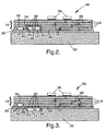
- FIG. 2 depicts a circuit board assembly 40 in which a power flip chip 14 is mounted on a low-temperature co-fired ceramic (LTCC) substrate 10 in accordance with a first embodiment of the present invention. While a circuit board assembly comprising an LTCC substrate 10 is preferred, the use of other laminate substrates, for example, organic circuit board substrate materials such as FR-4, is also within the scope of this invention.
- LTCC low-temperature co-fired ceramic
- the substrate 10 is a monolithic structure made up of multiple ceramic layers 12 bonded to each other, with thick-film conductors 30 located within the substrate 10 between adjacent layers 12.
- the substrate 10 is fabricated using individual green tapes on which the thick-film conductor pastes are deposited which, after stacking and firing at a temperature of, for example up to about 900°C, form the ceramic layers 12 and conductors 30, respectively.
- Other passive circuit components such as resistors and capacitors, may also be fabricated within the substrate 10 in this manner.
- conductors 30 on adjacent layers 12 are electrically interconnected with conductive interconnect vias 18.
- each of the ceramic layers 12 preferably contains a mixture of electrically-nonconductive materials, typically glass and ceramic particles that, when fired, fuse to form a rigid monolithic structure.
- a suitable fired composition for the ceramic layers 12 include, by weight, about 30% to about 100% of a glass frit material such as BaO-CaO-SiO 2- Al 2 O 3 -TiO 2 , with the balance being essentially a ceramic material such as Al 2 O 3 .
- Suitable thicknesses for the individual ceramic layers 12 are about 50 to about 250 micrometers, and a suitable thickness for the substrate 10 is about 250 to about 1500 micrometers.
- the flip chip 14 is shown located within a cavity 24 in a surface 26 of the substrate 10.
- the cavity 24 is defined by aligned openings through the two ceramic layers 12 nearest the substrate surface 26.
- the depth of the cavity 24 is determined by the number of ceramic layers 12 in which the aligned openings were made.
- the openings can be formed by, for example, punching the green tapes (not shown) used to form the two ceramic layers 12. In this manner, the width, length, and depth of the cavity 24 can be readily sized for the chip 14 to be placed in the cavity 24.
- the non-active backside surface of the chip 14 is substantially coplanar with the surface 26 of the substrate 10.
- the bottom of the cavity 24 is formed by a base wall 28 defined by the ceramic layer 12 next to the innermost ceramic layer 12 in which the aligned openings were formed (in the embodiment shown, the ceramic layer 12 that is third closest to the substrate surface 26).
- Conductors 30 present on the base wall 28 (and therefore between the second and third ceramic layers 12) are exposed within the cavity 24.
- the flip chip 14 is electrically connected and physically attached to the conductors 30 on the base wall 28 with multiple solder bumps 32 located on the active frontside of the chip 14.
- the flip chip 14 is preferably underfilled with a suitable underfill material 34 to reduce thermal stresses on the solder bumps 32.
- the preferred underfill material 34 is either an unfilled no-flow or capillary underfill material. If a no-flow material, the underfill material 34 is deposited (dispensed) onto the surface of the cavity base wall 28, the flip chip 14 is then placed through the underfill material 34 and onto the base wall 28 to allow the solder bumps 32 to be attached (reflow soldered) to the conductors 30. If the underfill material 34 is a capillary material, the flip chip 14 is attached to the conductors 30 on the substrate 10 by a reflow solder process, after which the substrate 10 is placed on a heated surface and the capillary underfill material 34 is dispensed around the perimeter of the flip chip 14, all within the confines of the walls of the cavity 24.
- the heat applied to the substrate 10 causes the underfill material 34 to spread between the flip chip 14 and the substrate 10, preferably to the extent that the underfill material 34 covers the entire surface area of the chip 14 and surrounds solder bumps 32.
- a secondary dispense of underfill material 34 may be necessary to fill the cavity 24.
- the chip 14 and a capillary-type underfill 34 may substantially fill the cavity 24, such that the cavity 24 is void-free.
- heat dissipated by the flip chip 14 is conducted away from the flip chip 14 to a heat sink 22 to which the substrate 10 is bonded with an adhesive 20.
- a suitable bondline thickness for the adhesive 20 is in a range of about 75 to about 375 micrometers.
- the bondline thickness of the adhesive 20 between the chip 14 and heat sink 22 is dependent on the ratio of the contact area of the chip 14 with the adhesive 22 to the contact area between the substrate 10 and the adhesive 20.
- the backside of the chip 14 is directly attached to the heat sink 22 with a solder material 36, such that the thermal path is directly between the chip 14 and heat sink 22 through the solder material 36.
- solder material 36 preferred materials for the heat sink 22 include plated or unplated aluminum and its alloys, copper and its alloys, plated steel, or a composite such as Cu/Mo/Cu, though other materials could be used.
- the solder material 36 preferably has a lower melting temperature than the solder bumps 32.
- the solder material 36 could be eliminated, such that heat dissipated by the flip chip 14 is conducted to the heat sink 22 solely through the adhesive 20.
- the heat sink 22 is not required to be formed of a solderable material.
- the thermal conductivity of the adhesive 20 becomes of greater importance.
- Heat transfer through the adhesive 20 can be promoted by forming the adhesive 20 of an adhesive matrix material (e.g., an epoxy) that contains a dispersion of metal and/or ceramic particles.
- heat transfer through the adhesive 20 can be promoted by minimizing the thickness of the adhesive 20 through which heat is conducted.
- a sufficient adhesive bondline thickness must exist to ensure a reliable bond between the chip 14 and heat sink 22. In the absence of the solder material 36, a suitable bondline thickness for the adhesive 20 between the chip 14 and heat sink 22 is believed to be about 25 to about 125 micrometers.
- FIG. 1 In addition to the power flip chip 14, other circuit devices are shown as being mounted to the substrate 10.
- various passive and active devices 38 are shown attached to the surface of the substrate 10 opposite the heat sink 22.
- Figure 2 also depicts a passive device 42 within a second cavity 44 formed in the surface 26 of the substrate 10.
- the cavity 44 can be fabricated in essentially the same manner as the cavity 24 for the flip chip 14, with electrical connection of the device 42 being through conductors 30 between the ceramic layers 12 nearest the heat sink 22.
- a surface of the device 42 is substantially coplanar with the surface 26 of the substrate 10, providing a thermal path from the device 42 to the heat sink 22 through the adhesive 20.
- the embodiment of Figure 2 does not rely on thermal vias that extend through the substrate 10 to conduct heat from the chip 14 to the heat sink 22. Instead, the layer of solder material 36 provides a direct path for heat transfer between the chip 14 and the heat sink 22, such that the relatively poor heat transfer characteristics of the substrate 10 do not pose a limitation to the thermal management of the chip 14.
- Figure 3 depicts a circuit board assembly 50 in accordance with a second embodiment of the invention in which, for convenience, corresponding components are identified with the same reference numbers as those used in Figure 2.
- a power flip chip 14 is mounted on an LTCC substrate 10 made up of multiple ceramic layers 12.
- the embodiment of Figure 3 primarily differs from Figure 2 by its location of the cavity 24 within the heat sink 22 instead of the substrate 10.
- Multiple solder bumps 32 on the active frontside of the chip 14 electrically and physically attach the chip 14 to conductors 30 on the surface 26 of the substrate 10.
- the non-active backside of the chip 14 may be bonded to the bottom of the cavity 24 with solder (not shown) or a portion of the adhesive 20 that bonds the heat sink 22 to the substrate 10.
- An advantage of this embodiment is that heat transfer occurs vertically from the chip 14 to the heat sink 22, as well as laterally into the heat sink 22 through the walls of the cavity 24.
- a desired effect is that the primary thermal path for the power flip chip 14 is through a solder material 36 or a thermally-conductive adhesive 20, and not through the LTCC substrate 10 on which the chip 14 is mounted.
- the relatively poor heat transfer characteristics of the substrate 10 do not pose a limitation to the thermal management of the chip 14, and the maximum steady-state and transient temperatures of the chip 14 can be significantly reduced in comparison to prior art LTCC substrates that rely on thermal vias ( Figure 1).
- the process of making the substrate 10 can be achieved without changing any of the fundamental steps of a conventional LTCC process. As such, the process of this invention will not be described in any detail.
- individual green tapes are blanked from a green ceramic tape roll formulated to contain a binder along with the appropriate glass frit, ceramic, etc., so that when fired the tapes will yield the desired composition for the ceramic layers 12 of the substrate 10.
- the green tapes undergo via punching to yield through-hole vias for the interconnect vias 18.
- the openings can also be formed that will define the cavities 24 and 44 in the substrate 10 depicted in Figure 2.
- the through-hole vias are then filled with a suitable conductive paste, which on firing will yield the interconnect vias 18.
- conductive paste is printed on the green tapes to form, on firing, the conductors 30.
- Suitable pastes can also be deposited at this time to form any thick-film resistors, etc., required for the circuitry of the substrate 10.
- Conventional LTCC processing can then be performed, including collating and laminating the tapes, so that the tapes are superimposed, i.e., the edges of the tapes are aligned.
- the resulting green substrate is then co-fired, during which the binders within the tapes and their components (e.g., vias 18, conductors 30, etc.) are burned off and the remaining inorganic components are fused.
- the flip chip 14 is reflow soldered to the substrate 10 and the heat sink 22 is bonded to the substrate 10 with the adhesive 20. If the cavity 24 is located in the substrate 10 ( Figure 2), the flip chip 14 is placed in the cavity 24 (after dispensing the underfill material 34 if a no-flow underfill is used, or before dispensing the underfill material 34 if a capillary-type underfill is used) so that its solder bumps 32 register with their respective conductors 30 on the cavity base wall 28.
- the flip chip 14 is placed on the substrate surface 26 so that its solder bumps 32 register with their respective conductors 30 on the substrate surface 26. Thereafter, the chip 14 and any other surface-mount devices 38 are reflow soldered to their respective conductors 30, followed by bonding of the heat sink 22 to the substrate 10.
Abstract

Description
- The present invention generally relates to thermal management of electronic circuit components. More particularly, this invention relates to a circuit board-heat sink structure with an interior cavity containing a surface-mount device thermally coupled to the heat sink to provide enhanced thermal management of the device.
- A variety of approaches are known for dissipating heat generated by semiconductor devices, such as integrated circuit (IC) chips. One method is to use a flex circuit laminated or bonded to a heat sink. If the flex circuit material is sufficiently thin, this approach can employ a highly conductive path formed by plated vias through the flex circuit to the heat sink. Another method is to equip a printed circuit board (PCB) with an innerlayer heat sink that is the same size or larger than the PCB to provide a large heat sink for the entire board, and rely on conduction through the PCB material to the heat sink beneath. High-power IC chips, such as power flip chips, are often mounted to substrates formed of a ceramic material such as alumina (Al2O3) or another ceramic material.
- Laminate-type ceramic substrates known as low temperature co-fired ceramics (LTCC) have a number of process-related advantages over conventional ceramic substrates. LTCC substrates are conventionally made up of multiple green tapes containing a mixture of glass and ceramic fillers in an organic binder. The tapes are collated (stacked), laminated, and then fired (co-fired), during which the organic binders within the laminate stack are burned off and the remaining materials form, according to the combined composition, a monolithic ceramic substrate. Though having the above-noted processing advantages, LTCC substrates have relatively low thermal conductivities, typically about 3 W/mK as compared to about 20 W/mK for alumina.
Consequently, LTCC substrates have been formed with green tapes containing a metal powder to promote heat dissipation through the substrate. However, a limitation of this approach is that the resulting metal-containing layers of the LTCC substrate are also electrically conductive to some degree. As an example, U.S. Patent No. 6,690,583 to Bergstedt et al. discloses a thermally-conductive LTCC substrate formed of a metal-containing tape and having surface cavities in which circuit devices are contained. Because of the electrical conductivity of the LTCC substrate, electrical connections must be made to the devices by depositing a dielectric layer over the substrate and the devices within its cavities, and then forming contacts through the dielectric layer to the devices. An alternative approach disclosed in U.S. Patent No. 5,386,339 to Polinski, Sr., is to form a limited thermally-conductive path through an otherwise conventional (dielectric) LTCC by defining a hole in a stack of dielectric green tapes, and then filling the hole with green tapes containing a thermally conductive material. On firing, the tapes form an LTCC substrate in which a vertical thermally-conductive path is present for conducting heat through the thickness of the substrate. - In other applications where individual layers of an LTCC substrate are to carry conductor patterns, resistors, etc., each ceramic layer is formed by a green tape containing only a mixture of glass and ceramic fillers in a binder. Thick-film conductors, resistors, etc., are printed on individual tapes prior to collating and laminating the tapes. The tapes, along with their conductors and resistors, are then co-fired, during which their respective binders burn off and the remaining materials form, according to their compositions, ceramic (dielectric) and metallic (conductive) materials. Because of the circuit components and their associated interconnect vias within the LTCC substrate, improved thermal conductivity cannot be obtained by the use of metal-containing ceramic layers. A solution to this problem is represented in Figure 1, and involves forming
multiple vias 116 through the thickness of anLTCC substrate 110 to conduct heat in a vertical direction from a die-and-wiretype power chip 114. Thethermal vias 116 are formed by punching vias in each green tape and then filling the vias with a metal such as silver prior to printing the conductors, resistors, etc.Interconnect vias 118 required to electrically interconnect components on different layers of theLTCC substrate 110 can be formed and filled at the same time as thethermal vias 116. The tapes are then laminated so that the filled vias are aligned to form through-vias, after which the tapes are fired such that the via fill material is co-fired along with conductor and resistor materials printed on surfaces of individual tapes. The entire LTCC substrate 110 (composed of bonded ceramic layers 112) is then bonded with an adhesive 120 to aheat sink 122 so that thethermal vias 116 conduct heat from thechip 114 to theheat sink 122. - While able to promote the conduction of heat away from power devices, thermal vias incur additional processing and material costs, reduce routing density, and can limit design flexibility. Furthermore, thermal vias may be inadequate to achieve suitable thermal management of certain power devices, particularly devices of the flip-chip type. For example, thermal vias alone can be inadequate because the solder bumps of a flip-chip device provide the primary thermal path from the device through the substrate. Compared to the overall die size, the contact area of each bump is relatively small, such that the bumps provide a limited thermal path to the substrate. Furthermore, the number of thermal vias that can be employed to conduct heat to and through the substrate is limited by the number of solder bumps and the configuration of the solder bump pattern. In addition, the use of thermal vias is complicated by the fact that the solder bumps usually require electrical isolation as a result of also providing the electrical connection between the device and the substrate.
- In view of the above, further improvements in the construction and processing of LTCC substrates would be desirable to improve thermal management of power IC's, and particularly flip-chip power IC's, while retaining the process-related advantages of LTCC's.
- The present invention provides a circuit board assembly having a laminate construction, such as an LTCC ceramic substrate. The substrate is assembled with a heat sink to yield an assembly that provides improved thermal management of one or more power circuit devices mounted to the substrate.
- According to a first aspect of the invention, the substrate is made up of a plurality of layers bonded to each other, such as a co-fired substrate made up of a plurality of ceramic layers. Conductor lines are present on at least some of the substrate layers so as to be between adjacent pairs of the substrate layers. A heat sink is bonded to a first surface of the substrate, and a cavity is defined by and between the heat sink and the substrate. For example, the cavity may be defined entirely within the first surface of the substrate, entirely within the opposing surface of the heat sink, or partially in both. If the cavity is formed entirely within the substrate, the surface of the device is preferably at least coplanar with the first surface of the substrate, i.e., the surface of the device is approximately coplanar with or projects beyond the first surface of the substrate. A base wall of the cavity is defined by one of the substrate layers so that conductor lines thereof are present on the base wall. A surface-mount circuit device is received within the cavity, mounted to the cavity base wall, and electrically connected to the conductor lines on the base wall. The device is received within the cavity such that a surface of the device contacts a surface region of the heat sink. The surface of the device is bonded to the surface region of the heat sink to provide a substantially direct thermal path from the device to the heat sink.
- According to the invention, the substrate as described above does not require thermal vias that extend through the substrate from the surface-mount circuit device to one of the surfaces of the substrate. Instead, thermal management is achieved by providing a short thermal path directly from the device to the heat sink bonded to the surface of the substrate. The thermal path may include the material with which the heat sink is bonded to the substrate, or another material with better thermal conductivity. By eliminating the requirement for thermal vias, the routing densities of the conductor lines within the substrate are not compromised. Furthermore, if the device is a flip-chip, thermal management is not limited by the number of solder bumps, the configuration of the solder bump pattern, or the requirement for electrical isolation of the solder bumps.
- The above advantages of the invention can be achieved without changing any of the fundamental steps of the LTCC process. As such, the processing and structural advantages of LTCC substrates, including the ability to produce conductor lines and other circuit components by photoimaging techniques, can be retained by the invention.
- Other objects and advantages of this invention will be better appreciated from the following detailed description.
-
- Figure 1 shows an LTCC substrate with thermal vias in accordance with the prior art.
- Figures 2 and 3 show circuit board assemblies in accordance with three embodiments of the present invention.
- Figure 2 depicts a
circuit board assembly 40 in which apower flip chip 14 is mounted on a low-temperature co-fired ceramic (LTCC)substrate 10 in accordance with a first embodiment of the present invention. While a circuit board assembly comprising anLTCC substrate 10 is preferred, the use of other laminate substrates, for example, organic circuit board substrate materials such as FR-4, is also within the scope of this invention. - As an LTCC, the
substrate 10 is a monolithic structure made up of multipleceramic layers 12 bonded to each other, with thick-film conductors 30 located within thesubstrate 10 betweenadjacent layers 12. As with known LTCC processes, thesubstrate 10 is fabricated using individual green tapes on which the thick-film conductor pastes are deposited which, after stacking and firing at a temperature of, for example up to about 900°C, form theceramic layers 12 andconductors 30, respectively. Other passive circuit components, such as resistors and capacitors, may also be fabricated within thesubstrate 10 in this manner. Also consistent with LTCC substrates of the past,conductors 30 onadjacent layers 12 are electrically interconnected withconductive interconnect vias 18. Thevias 18 are preferably filled through-holes, wherein holes having a diameter of about 3 to about 20 mils (about 75 to about 500 micrometers) are formed in the green tapes and then filled with a suitable conductive material prior to stacking and firing the green tapes. As with prior art LTCC substrates, each of theceramic layers 12 preferably contains a mixture of electrically-nonconductive materials, typically glass and ceramic particles that, when fired, fuse to form a rigid monolithic structure. A suitable fired composition for theceramic layers 12 include, by weight, about 30% to about 100% of a glass frit material such as BaO-CaO-SiO2-Al2O3-TiO2, with the balance being essentially a ceramic material such as Al2O3. Suitable thicknesses for the individualceramic layers 12 are about 50 to about 250 micrometers, and a suitable thickness for thesubstrate 10 is about 250 to about 1500 micrometers. - The
flip chip 14 is shown located within a cavity 24 in asurface 26 of thesubstrate 10. As evident from Figure 2, the cavity 24 is defined by aligned openings through the twoceramic layers 12 nearest thesubstrate surface 26. The depth of the cavity 24 is determined by the number ofceramic layers 12 in which the aligned openings were made. The openings can be formed by, for example, punching the green tapes (not shown) used to form the twoceramic layers 12. In this manner, the width, length, and depth of the cavity 24 can be readily sized for thechip 14 to be placed in the cavity 24. In Figure 2, the non-active backside surface of thechip 14 is substantially coplanar with thesurface 26 of thesubstrate 10. - In the embodiment shown, the bottom of the cavity 24 is formed by a
base wall 28 defined by theceramic layer 12 next to the innermostceramic layer 12 in which the aligned openings were formed (in the embodiment shown, theceramic layer 12 that is third closest to the substrate surface 26).Conductors 30 present on the base wall 28 (and therefore between the second and third ceramic layers 12) are exposed within the cavity 24. According to known flip chip procedures, theflip chip 14 is electrically connected and physically attached to theconductors 30 on thebase wall 28 with multiple solder bumps 32 located on the active frontside of thechip 14. Also in accordance with known flip chip practices, theflip chip 14 is preferably underfilled with asuitable underfill material 34 to reduce thermal stresses on the solder bumps 32. Thepreferred underfill material 34 is either an unfilled no-flow or capillary underfill material. If a no-flow material, theunderfill material 34 is deposited (dispensed) onto the surface of thecavity base wall 28, theflip chip 14 is then placed through theunderfill material 34 and onto thebase wall 28 to allow the solder bumps 32 to be attached (reflow soldered) to theconductors 30. If theunderfill material 34 is a capillary material, theflip chip 14 is attached to theconductors 30 on thesubstrate 10 by a reflow solder process, after which thesubstrate 10 is placed on a heated surface and thecapillary underfill material 34 is dispensed around the perimeter of theflip chip 14, all within the confines of the walls of the cavity 24. The heat applied to thesubstrate 10 causes theunderfill material 34 to spread between theflip chip 14 and thesubstrate 10, preferably to the extent that theunderfill material 34 covers the entire surface area of thechip 14 and surrounds solder bumps 32. A secondary dispense ofunderfill material 34 may be necessary to fill the cavity 24. As seen in Figure 2, thechip 14 and a capillary-type underfill 34 may substantially fill the cavity 24, such that the cavity 24 is void-free. - According to a preferred aspect of the invention, heat dissipated by the
flip chip 14 is conducted away from theflip chip 14 to aheat sink 22 to which thesubstrate 10 is bonded with an adhesive 20. A suitable bondline thickness for the adhesive 20 is in a range of about 75 to about 375 micrometers. Generally, the bondline thickness of the adhesive 20 between thechip 14 andheat sink 22 is dependent on the ratio of the contact area of thechip 14 with the adhesive 22 to the contact area between thesubstrate 10 and the adhesive 20. - As depicted in Figure 2, the backside of the
chip 14 is directly attached to theheat sink 22 with asolder material 36, such that the thermal path is directly between thechip 14 andheat sink 22 through thesolder material 36. For use with thesolder material 36, preferred materials for theheat sink 22 include plated or unplated aluminum and its alloys, copper and its alloys, plated steel, or a composite such as Cu/Mo/Cu, though other materials could be used. To prevent reflowing the solder bumps 32 on the frontside of thechip 14 during soldering of thechip 14 to theheat sink 22, thesolder material 36 preferably has a lower melting temperature than the solder bumps 32. - As an alternative, the
solder material 36 could be eliminated, such that heat dissipated by theflip chip 14 is conducted to theheat sink 22 solely through the adhesive 20. In such an embodiment, theheat sink 22 is not required to be formed of a solderable material. However, the thermal conductivity of the adhesive 20 becomes of greater importance. Heat transfer through the adhesive 20 can be promoted by forming the adhesive 20 of an adhesive matrix material (e.g., an epoxy) that contains a dispersion of metal and/or ceramic particles. Alternatively or in addition, heat transfer through the adhesive 20 can be promoted by minimizing the thickness of the adhesive 20 through which heat is conducted. However, if thesolder material 36 is not employed, a sufficient adhesive bondline thickness must exist to ensure a reliable bond between thechip 14 andheat sink 22. In the absence of thesolder material 36, a suitable bondline thickness for the adhesive 20 between thechip 14 andheat sink 22 is believed to be about 25 to about 125 micrometers. - In addition to the
power flip chip 14, other circuit devices are shown as being mounted to thesubstrate 10. For example, various passive andactive devices 38 are shown attached to the surface of thesubstrate 10 opposite theheat sink 22. Figure 2 also depicts apassive device 42 within a second cavity 44 formed in thesurface 26 of thesubstrate 10. The cavity 44 can be fabricated in essentially the same manner as the cavity 24 for theflip chip 14, with electrical connection of thedevice 42 being throughconductors 30 between theceramic layers 12 nearest theheat sink 22. A surface of thedevice 42 is substantially coplanar with thesurface 26 of thesubstrate 10, providing a thermal path from thedevice 42 to theheat sink 22 through the adhesive 20. - In view of the above, the embodiment of Figure 2 does not rely on thermal vias that extend through the
substrate 10 to conduct heat from thechip 14 to theheat sink 22. Instead, the layer ofsolder material 36 provides a direct path for heat transfer between thechip 14 and theheat sink 22, such that the relatively poor heat transfer characteristics of thesubstrate 10 do not pose a limitation to the thermal management of thechip 14. - Figure 3 depicts a
circuit board assembly 50 in accordance with a second embodiment of the invention in which, for convenience, corresponding components are identified with the same reference numbers as those used in Figure 2. As such, apower flip chip 14 is mounted on anLTCC substrate 10 made up of multipleceramic layers 12. The embodiment of Figure 3 primarily differs from Figure 2 by its location of the cavity 24 within theheat sink 22 instead of thesubstrate 10. Multiple solder bumps 32 on the active frontside of thechip 14 electrically and physically attach thechip 14 toconductors 30 on thesurface 26 of thesubstrate 10. The non-active backside of thechip 14 may be bonded to the bottom of the cavity 24 with solder (not shown) or a portion of the adhesive 20 that bonds theheat sink 22 to thesubstrate 10. An advantage of this embodiment is that heat transfer occurs vertically from thechip 14 to theheat sink 22, as well as laterally into theheat sink 22 through the walls of the cavity 24. - With each of the embodiments represented in Figures 2 and 3, a desired effect is that the primary thermal path for the
power flip chip 14 is through asolder material 36 or a thermally-conductive adhesive 20, and not through theLTCC substrate 10 on which thechip 14 is mounted. As such, the relatively poor heat transfer characteristics of thesubstrate 10 do not pose a limitation to the thermal management of thechip 14, and the maximum steady-state and transient temperatures of thechip 14 can be significantly reduced in comparison to prior art LTCC substrates that rely on thermal vias (Figure 1). - The process of making the
substrate 10 can be achieved without changing any of the fundamental steps of a conventional LTCC process. As such, the process of this invention will not be described in any detail. In a suitable process consistent with LTCC processes, individual green tapes are blanked from a green ceramic tape roll formulated to contain a binder along with the appropriate glass frit, ceramic, etc., so that when fired the tapes will yield the desired composition for theceramic layers 12 of thesubstrate 10. Following blanking, the green tapes undergo via punching to yield through-hole vias for theinterconnect vias 18. At this time, the openings can also be formed that will define the cavities 24 and 44 in thesubstrate 10 depicted in Figure 2. The through-hole vias are then filled with a suitable conductive paste, which on firing will yield theinterconnect vias 18. Thereafter, conductive paste is printed on the green tapes to form, on firing, theconductors 30. Suitable pastes can also be deposited at this time to form any thick-film resistors, etc., required for the circuitry of thesubstrate 10. Conventional LTCC processing can then be performed, including collating and laminating the tapes, so that the tapes are superimposed, i.e., the edges of the tapes are aligned. The resulting green substrate is then co-fired, during which the binders within the tapes and their components (e.g., vias 18,conductors 30, etc.) are burned off and the remaining inorganic components are fused. - After conventional post-printing and post-firing process steps such as resistor trimming and electrical testing are carried out, the
flip chip 14 is reflow soldered to thesubstrate 10 and theheat sink 22 is bonded to thesubstrate 10 with the adhesive 20. If the cavity 24 is located in the substrate 10 (Figure 2), theflip chip 14 is placed in the cavity 24 (after dispensing theunderfill material 34 if a no-flow underfill is used, or before dispensing theunderfill material 34 if a capillary-type underfill is used) so that its solder bumps 32 register with theirrespective conductors 30 on thecavity base wall 28. If the cavity 24 is located in the heat sink 22 (Figure 3), theflip chip 14 is placed on thesubstrate surface 26 so that its solder bumps 32 register with theirrespective conductors 30 on thesubstrate surface 26. Thereafter, thechip 14 and any other surface-mount devices 38 are reflow soldered to theirrespective conductors 30, followed by bonding of theheat sink 22 to thesubstrate 10. - While the invention has been described in terms of particular embodiments, it is apparent that other forms could be adopted by one skilled in the art. Accordingly, the scope of the invention is to be limited only by the following claims.
Claims (20)
- A circuit board assembly (40,50) comprising a substrate (10), a heat sink (22) bonded to a first surface (26) of the substrate (10), and a surface-mount circuit device (14) mounted on the substrate (10), the substrate (10) comprising a plurality of layers (12) bonded to each other and conductor lines (30) on at least some of the layers (12) so as to be between adjacent pairs of the layers (12), characterized in that:the heat sink (22) and the substrate (10) define a cavity (24) therebetween, the cavity (24) having a base wall (28) defined by one of the layers (12) with conductor lines (30) thereof being present on the base wall (28), the device (14) is mounted to the base wall (28) of the cavity (24) so as to be received within the cavity (24), the device (14) is electrically connected to the conductor lines (30) on the base wall (28) of the cavity (24), and the device (14) has a surface bonded to the heat sink (22) to provide a thermal path from the device (14) to the heat sink (22).
- A circuit board assembly (40,50) according to claim 1, further comprising solder material (36) that directly bonds the surface of the device (14) to the heat sink (22), the thermal path from the device (14) to the heat sink (22) being through the solder material (36).
- A circuit board assembly (40,50) according to claim 1, characterized in that the thermal path from the device (14) to the heat sink (22) is through an adhesive bonding material (20) that also bonds the substrate (10) to the heat sink (22).
- A circuit board assembly (40,50) according to claim 3, characterized in that the adhesive bonding material (20) comprises an adhesive matrix containing particles that are more thermally conductive than the adhesive matrix.
- A circuit board assembly (40,50) according to claim 1, characterized in that the device (14) is a flip chip device (14) electrically connected to the conductor lines (30) on the base wall (28) of the cavity (24) with a plurality of solder connections (32).
- A circuit board assembly (40) according to claim 1, characterized in that the cavity (24) is defined entirely within the substrate (10), the base wall (28) of the cavity (24) is defined by one of the layers (12) beneath the first surface (26) of the substrate (10), and the surface of the device (14) is substantially coplanar with the first surface (26) of the substrate (10).
- A circuit board assembly (50) according to claim 1, characterized in that the cavity (24) is defined entirely within the heat sink (22), the base wall (28) of the cavity (24) is defined by the first surface (26) of the substrate (10), and the surface of the device (14) projects beyond the first surface (26) of the substrate (10).
- A circuit board assembly (40,50) according to claim 1, further comprising a circuit device (38) mounted to a second surface of the substrate (10) opposite the first surface (26).
- A circuit board assembly (40,50) according to claim 1, characterized in that the substrate (10) is a low-temperature co-fired ceramic substrate (10).
- A circuit board assembly (40,50) according to claim 1, characterized in that the substrate (10) does not contain any thermal vias extending through the substrate (10) from the device (14) to the first surface (26).
- A circuit board assembly (40,50) according to claim 1, further comprising:a second cavity (44) in the first surface (26) of the substrate (10), the second cavity (44) having a wall defined by one of the layers (12) with conductor lines (30) thereof on the wall; anda passive electronic component (42) mounted to the wall of the second cavity (44) so as to be received entirely within the second cavity (44), the passive electronic component (42) being electrically connected to the conductor lines (30) on the wall of the second cavity (44).
- A circuit board assembly (40,50) according to claim 11, characterized in that the passive electronic component (42) has a surface substantially coplanar with the first surface (26) of the substrate (10).
- A circuit board assembly (40,50) according to claim 12, characterized in that the heat sink (22) is bonded with a bonding material (20) to the surface of the passive electronic component (42) to provide a thermal path from the passive electronic component (42) to the heat sink (22) through the bonding material (20).
- A circuit board assembly (40,50) comprising a substrate (10), a heat sink (22) bonded to a first surface (26) of the substrate (10), and a flip-chip circuit device (14) mounted on the substrate (10), the substrate (10) comprising a plurality of layers (12) bonded to each other and conductor lines (30) on at least some of the layers (12) so as to be between adjacent pairs of the layers (12), characterized in that:the substrate (10) is a low-temperature co-fired ceramic substrate (10) and the layers (12) thereof are ceramic layers (12), the heat sink (22) and the substrate (10) define a cavity (24) therebetween in the first surface (26) of the substrate (10), the cavity (24) having a base wall (28) defined by one of the ceramic layers (12) with conductor lines (30) thereof on the base wall (28), the device (14) is mounted to the base wall (28) of the cavity (24) so as to be received within the cavity (24), the device (14) is electrically connected to the conductor lines (30) on the base wall (28) of the cavity (24) with a plurality of solder connections (32), the device (14) has a surface that sufficiently projects from the base wall (28) of the cavity (24) so as to be at least approximately coplanar with the first surface (26) of the substrate (10), the heat sink (22) is bonded to the surface of the device (14) to provide a thermal path from the device (14) to the heat sink (22), and the cavity (24) is substantially entirely filled by the device (14) and an underfill material (34).
- A circuit board assembly (40,50) according to claim 14, characterized in that the surface of the device (14) projects beyond the first surface (26) of the substrate (10), the circuit board assembly (40,50) further comprising solder material (34) that directly bonds the surface of the device (14) to the heat sink (22), the thermal path from the device (14) to the heat sink (22) being through the solder material (34).
- A circuit board assembly (40,50) according to claim 14, characterized in that the surface of the device (14) is substantially coplanar with the first surface (26) of the substrate (10), and the thermal path from the device (14) to the heat sink (22) is through an adhesive bonding material (20) that also bonds the substrate (10) to the heat sink (22).
- A circuit board assembly (40,50) according to claim 14, further comprising a circuit device (38) mounted to a second surface of the substrate (10) opposite the first surface (26).
- A circuit board assembly (40,50) according to claim 14, characterized in that the substrate (10) does not contain any thermal vias extending through the substrate (10) from the device (14) to the first surface (26).
- A circuit board assembly (40,50) according to claim 14, further comprising:a second cavity (44) in the first surface (26) of the substrate (10), the second cavity (44) having a wall defined by one of the ceramic layers (12) with conductor lines (30) thereof on the wall; anda passive electronic component (42) mounted to the wall of the second cavity (44) so as to be received entirely within the second cavity (44), the passive electronic component (42) being electrically connected to the conductor lines (30) on the wall of the second cavity (44).
- A circuit board assembly (40,50) according to claim 19, characterized in that the passive electronic component (42) has a surface substantially coplanar with the first surface (26) of the substrate (10), and the heat sink (22) is bonded with an adhesive bonding material (20) to the surface of the passive electronic component (42) to provide a thermal path from the passive electronic component (42) to the heat sink (22) through the adhesive bonding material (20).
Applications Claiming Priority (1)
| Application Number | Priority Date | Filing Date | Title |
|---|---|---|---|
| US10/904,904 US7365273B2 (en) | 2004-12-03 | 2004-12-03 | Thermal management of surface-mount circuit devices |
Publications (2)
| Publication Number | Publication Date |
|---|---|
| EP1667226A2 true EP1667226A2 (en) | 2006-06-07 |
| EP1667226A3 EP1667226A3 (en) | 2008-10-22 |
Family
ID=35883811
Family Applications (1)
| Application Number | Title | Priority Date | Filing Date |
|---|---|---|---|
| EP05077632A Withdrawn EP1667226A3 (en) | 2004-12-03 | 2005-11-18 | Thermal management of surface-mount circuit devices |
Country Status (2)
| Country | Link |
|---|---|
| US (1) | US7365273B2 (en) |
| EP (1) | EP1667226A3 (en) |
Cited By (1)
| Publication number | Priority date | Publication date | Assignee | Title |
|---|---|---|---|---|
| WO2009016039A1 (en) * | 2007-08-01 | 2009-02-05 | Siemens Aktiengesellschaft | Electronic module having at least one component, particularly a semiconductor component, and method for the production thereof |
Families Citing this family (37)
| Publication number | Priority date | Publication date | Assignee | Title |
|---|---|---|---|---|
| TW503496B (en) | 2001-12-31 | 2002-09-21 | Megic Corp | Chip packaging structure and manufacturing process of the same |
| TW544882B (en) | 2001-12-31 | 2003-08-01 | Megic Corp | Chip package structure and process thereof |
| TW517361B (en) * | 2001-12-31 | 2003-01-11 | Megic Corp | Chip package structure and its manufacture process |
| TW584950B (en) | 2001-12-31 | 2004-04-21 | Megic Corp | Chip packaging structure and process thereof |
| US6673698B1 (en) | 2002-01-19 | 2004-01-06 | Megic Corporation | Thin film semiconductor package utilizing a glass substrate with composite polymer/metal interconnect layers |
| CN100508701C (en) * | 2004-10-22 | 2009-07-01 | 株式会社村田制作所 | Hybrid multilayer substrate and preparation method thereof |
| JP2006165175A (en) * | 2004-12-06 | 2006-06-22 | Alps Electric Co Ltd | Circuit component module, electronic circuit device, and circuit component module manufacturing method |
| US7310036B2 (en) | 2005-01-10 | 2007-12-18 | International Business Machines Corporation | Heat sink for integrated circuit devices |
| KR100737098B1 (en) * | 2006-03-16 | 2007-07-06 | 엘지이노텍 주식회사 | Shield device of electromagnetic inteference and production progress thereof |
| US9713258B2 (en) * | 2006-04-27 | 2017-07-18 | International Business Machines Corporation | Integrated circuit chip packaging |
| JP4821537B2 (en) * | 2006-09-26 | 2011-11-24 | 株式会社デンソー | Electronic control unit |
| US7808797B2 (en) * | 2006-12-11 | 2010-10-05 | Intel Corporation | Microelectronic substrate including embedded components and spacer layer and method of forming same |
| KR100825766B1 (en) * | 2007-04-26 | 2008-04-29 | 한국전자통신연구원 | Low temperature co-fired ceramic package and method of manufacturing the same |
| DE102007038514A1 (en) * | 2007-08-16 | 2009-02-19 | Robert Bosch Gmbh | Electrical circuit arrangement and method for producing an electrical circuit arrangement |
| JP5070014B2 (en) * | 2007-11-21 | 2012-11-07 | 株式会社豊田自動織機 | Heat dissipation device |
| JP2009130060A (en) * | 2007-11-21 | 2009-06-11 | Toyota Industries Corp | Heat dissipater |
| US8749038B2 (en) * | 2008-01-25 | 2014-06-10 | Azurewave Technologies, Inc. | Substrate module having an embedded phase-locked loop, integerated system using the same, and fabricating method thereof |
| WO2009118925A1 (en) * | 2008-03-27 | 2009-10-01 | イビデン株式会社 | Circuit board having built-in electronic parts and its manufacturing method |
| KR101089840B1 (en) * | 2009-04-01 | 2011-12-05 | 삼성전기주식회사 | Circuit board module and manufacturing method for the same |
| KR101015735B1 (en) * | 2009-07-02 | 2011-02-22 | 삼성전기주식회사 | Ceramic elements module and the manufacturing method |
| US8237252B2 (en) | 2009-07-22 | 2012-08-07 | Stats Chippac, Ltd. | Semiconductor device and method of embedding thermally conductive layer in interconnect structure for heat dissipation |
| US8848375B2 (en) * | 2009-09-24 | 2014-09-30 | Lear Corporation | System and method for reduced thermal resistance between a power electronics printed circuit board and a base plate |
| DE102010030525A1 (en) * | 2010-06-25 | 2011-12-29 | Zf Friedrichshafen Ag | Electronic control module |
| KR101289140B1 (en) * | 2010-09-28 | 2013-07-23 | 삼성전기주식회사 | Embedded substrate and a method for manufacturing the same |
| US9277645B2 (en) * | 2012-01-18 | 2016-03-01 | Covidien Lp | Method of manufacturing a printed circuit board |
| US20130229777A1 (en) * | 2012-03-01 | 2013-09-05 | Infineon Technologies Ag | Chip arrangements and methods for forming a chip arrangement |
| KR101928814B1 (en) | 2012-05-04 | 2018-12-14 | 한국전자통신연구원 | Wafer level packaged GaN power device and the manufacturing method thereof |
| JP6251739B2 (en) * | 2013-05-22 | 2017-12-20 | 株式会社カネカ | Heat dissipation structure |
| JP6341822B2 (en) * | 2014-09-26 | 2018-06-13 | 三菱電機株式会社 | Semiconductor device |
| US9496194B2 (en) * | 2014-11-07 | 2016-11-15 | International Business Machines Corporation | Customized module lid |
| FR3036917B1 (en) * | 2015-05-28 | 2018-11-02 | IFP Energies Nouvelles | ELECTRONIC DEVICE COMPRISING A PRINTED CIRCUIT BOARD WITH IMPROVED COOLING. |
| KR101666757B1 (en) * | 2015-07-13 | 2016-10-24 | 앰코 테크놀로지 코리아 주식회사 | Semiconductor package |
| US20170325327A1 (en) * | 2016-04-07 | 2017-11-09 | Massachusetts Institute Of Technology | Printed circuit board for high power components |
| US11355427B2 (en) * | 2016-07-01 | 2022-06-07 | Intel Corporation | Device, method and system for providing recessed interconnect structures of a substrate |
| DE102016222631A1 (en) * | 2016-11-17 | 2018-05-17 | Zf Friedrichshafen Ag | Printed circuit board assembly with an electrical component and a heat sink |
| DE102019100802A1 (en) * | 2019-01-14 | 2020-07-16 | Tdk Electronics Ag | LED module and use of the LED module |
| US11641720B2 (en) * | 2020-09-18 | 2023-05-02 | Unimicron Technology Corp. | Circuit board and manufacturing method thereof |
Citations (13)
| Publication number | Priority date | Publication date | Assignee | Title |
|---|---|---|---|---|
| EP0449640A1 (en) * | 1990-03-28 | 1991-10-02 | Mitsubishi Denki Kabushiki Kaisha | Method for mounting electrical components. |
| EP0865082A1 (en) * | 1995-11-28 | 1998-09-16 | Hitachi, Ltd. | Semiconductor device, process for producing the same, and packaged substrate |
| EP0883175A2 (en) * | 1997-06-03 | 1998-12-09 | Lsi Logic Corporation | High performance heat spreader for flip chip packages |
| US5905636A (en) * | 1995-11-06 | 1999-05-18 | International Business Machines Corporation | Heat dissipation apparatus and method for attaching a heat dissipation apparatus to an electronic device |
| EP0933816A2 (en) * | 1998-01-30 | 1999-08-04 | Taiyo Yuden Co., Ltd. | Hybrid module and methods for manufacturing and mounting thereof |
| US6008536A (en) * | 1997-06-23 | 1999-12-28 | Lsi Logic Corporation | Grid array device package including advanced heat transfer mechanisms |
| US6118177A (en) * | 1998-11-17 | 2000-09-12 | Lucent Technologies, Inc. | Heatspreader for a flip chip device, and method for connecting the heatspreader |
| US20010026957A1 (en) * | 1998-03-31 | 2001-10-04 | International Business Machines Corporation | Thermal enhancement approach using solder compositions in the liquid state |
| US20020033528A1 (en) * | 1998-11-16 | 2002-03-21 | Nec Corporation | Multichip module and method for manufacturing |
| US6411507B1 (en) * | 1998-02-13 | 2002-06-25 | Micron Technology, Inc. | Removing heat from integrated circuit devices mounted on a support structure |
| US20030134454A1 (en) * | 2002-01-16 | 2003-07-17 | Intel Corporation | Apparatus and method for containing excess thermal interface material |
| US6602739B1 (en) * | 2001-10-31 | 2003-08-05 | Lockheed Martin Corporation | Method for making multichip module substrates by encapsulating electrical conductors and filling gaps |
| US20030169575A1 (en) * | 2002-02-26 | 2003-09-11 | Kyocera Corporation | High frequency module |
Family Cites Families (17)
| Publication number | Priority date | Publication date | Assignee | Title |
|---|---|---|---|---|
| JPH0548000A (en) * | 1991-08-13 | 1993-02-26 | Fujitsu Ltd | Semiconductor device |
| US5386339A (en) | 1993-07-29 | 1995-01-31 | Hughes Aircraft Company | Monolithic microelectronic circuit package including low-temperature-cofired-ceramic (LTCC) tape dielectric structure and in-situ heat sink |
| TW373308B (en) * | 1995-02-24 | 1999-11-01 | Agere Systems Inc | Thin packaging of multi-chip modules with enhanced thermal/power management |
| US6125039A (en) * | 1996-07-31 | 2000-09-26 | Taiyo Yuden Co., Ltd. | Hybrid module |
| US5926371A (en) * | 1997-04-25 | 1999-07-20 | Advanced Micro Devices, Inc. | Heat transfer apparatus which accommodates elevational disparity across an upper surface of a surface-mounted semiconductor device |
| US6159764A (en) * | 1997-07-02 | 2000-12-12 | Micron Technology, Inc. | Varied-thickness heat sink for integrated circuit (IC) packages and method of fabricating IC packages |
| WO2000019516A1 (en) * | 1998-09-30 | 2000-04-06 | Seiko Epson Corporation | Semiconductor device, connection method for semiconductor chip, circuit board and electronic apparatus |
| SE515856C2 (en) | 1999-05-19 | 2001-10-22 | Ericsson Telefon Ab L M | Carrier for electronic components |
| US6487083B1 (en) * | 2000-08-10 | 2002-11-26 | Nortel Networks Ltd. | Multilayer circuit board |
| JP2002246503A (en) * | 2001-02-16 | 2002-08-30 | Philips Japan Ltd | Electronic component and its manufacturing method |
| US6742248B2 (en) * | 2001-05-14 | 2004-06-01 | The Boeing Company | Method of forming a soldered electrical connection |
| US6680441B2 (en) * | 2001-06-13 | 2004-01-20 | Denso Corporation | Printed wiring board with embedded electric device and method for manufacturing printed wiring board with embedded electric device |
| US6607942B1 (en) * | 2001-07-26 | 2003-08-19 | Taiwan Semiconductor Manufacturing Company | Method of fabricating as grooved heat spreader for stress reduction in an IC package |
| US6535388B1 (en) * | 2001-10-04 | 2003-03-18 | Intel Corporation | Wirebonded microelectronic packages including heat dissipation devices for heat removal from active surfaces thereof |
| US6933603B2 (en) * | 2002-07-11 | 2005-08-23 | Teledyne Technologies Incorporated | Multi-substrate layer semiconductor packages and method for making same |
| US7057896B2 (en) * | 2002-08-21 | 2006-06-06 | Matsushita Electric Industrial Co., Ltd. | Power module and production method thereof |
| US6816378B1 (en) * | 2003-04-28 | 2004-11-09 | Hewlett-Packard Development Company, L.P. | Stack up assembly |
-
2004
- 2004-12-03 US US10/904,904 patent/US7365273B2/en active Active
-
2005
- 2005-11-18 EP EP05077632A patent/EP1667226A3/en not_active Withdrawn
Patent Citations (13)
| Publication number | Priority date | Publication date | Assignee | Title |
|---|---|---|---|---|
| EP0449640A1 (en) * | 1990-03-28 | 1991-10-02 | Mitsubishi Denki Kabushiki Kaisha | Method for mounting electrical components. |
| US5905636A (en) * | 1995-11-06 | 1999-05-18 | International Business Machines Corporation | Heat dissipation apparatus and method for attaching a heat dissipation apparatus to an electronic device |
| EP0865082A1 (en) * | 1995-11-28 | 1998-09-16 | Hitachi, Ltd. | Semiconductor device, process for producing the same, and packaged substrate |
| EP0883175A2 (en) * | 1997-06-03 | 1998-12-09 | Lsi Logic Corporation | High performance heat spreader for flip chip packages |
| US6008536A (en) * | 1997-06-23 | 1999-12-28 | Lsi Logic Corporation | Grid array device package including advanced heat transfer mechanisms |
| EP0933816A2 (en) * | 1998-01-30 | 1999-08-04 | Taiyo Yuden Co., Ltd. | Hybrid module and methods for manufacturing and mounting thereof |
| US6411507B1 (en) * | 1998-02-13 | 2002-06-25 | Micron Technology, Inc. | Removing heat from integrated circuit devices mounted on a support structure |
| US20010026957A1 (en) * | 1998-03-31 | 2001-10-04 | International Business Machines Corporation | Thermal enhancement approach using solder compositions in the liquid state |
| US20020033528A1 (en) * | 1998-11-16 | 2002-03-21 | Nec Corporation | Multichip module and method for manufacturing |
| US6118177A (en) * | 1998-11-17 | 2000-09-12 | Lucent Technologies, Inc. | Heatspreader for a flip chip device, and method for connecting the heatspreader |
| US6602739B1 (en) * | 2001-10-31 | 2003-08-05 | Lockheed Martin Corporation | Method for making multichip module substrates by encapsulating electrical conductors and filling gaps |
| US20030134454A1 (en) * | 2002-01-16 | 2003-07-17 | Intel Corporation | Apparatus and method for containing excess thermal interface material |
| US20030169575A1 (en) * | 2002-02-26 | 2003-09-11 | Kyocera Corporation | High frequency module |
Cited By (1)
| Publication number | Priority date | Publication date | Assignee | Title |
|---|---|---|---|---|
| WO2009016039A1 (en) * | 2007-08-01 | 2009-02-05 | Siemens Aktiengesellschaft | Electronic module having at least one component, particularly a semiconductor component, and method for the production thereof |
Also Published As
| Publication number | Publication date |
|---|---|
| US20060120058A1 (en) | 2006-06-08 |
| US7365273B2 (en) | 2008-04-29 |
| EP1667226A3 (en) | 2008-10-22 |
Similar Documents
| Publication | Publication Date | Title |
|---|---|---|
| US7365273B2 (en) | Thermal management of surface-mount circuit devices | |
| US7269017B2 (en) | Thermal management of surface-mount circuit devices on laminate ceramic substrate | |
| US7574793B2 (en) | Process of forming a laminate ceramic circuit board | |
| US8139368B2 (en) | Component-containing module | |
| JP2548602B2 (en) | Semiconductor mounting module | |
| US6262477B1 (en) | Ball grid array electronic package | |
| US7650694B2 (en) | Method for forming multilayer substrate | |
| US6395582B1 (en) | Methods for forming ground vias in semiconductor packages | |
| JP4310467B2 (en) | Composite multilayer substrate and manufacturing method thereof | |
| US6739047B2 (en) | Method of making ceramic multilayer circuit boards mounted in a patterned metal support substrate | |
| US6219253B1 (en) | Molded electronic package, method of preparation using build up technology and method of shielding | |
| JPH06291216A (en) | Substrate and ceramic package | |
| JP3266505B2 (en) | Multilayer circuit board | |
| EP1387403A2 (en) | Semiconductor packaging | |
| US9269685B2 (en) | Integrated circuit package and packaging methods | |
| US6441486B1 (en) | BGA substrate via structure | |
| EP0987748A2 (en) | Multilayered circuit board for semiconductor chip module, and method of manufacturing the same | |
| US9105562B2 (en) | Integrated circuit package and packaging methods | |
| EP1240667B1 (en) | Integrated circuit package | |
| US6408511B1 (en) | Method of creating an enhanced BGA attachment in a low-temperature co-fired ceramic (LTCC) substrate | |
| US7820490B2 (en) | Method for LTCC circuitry | |
| JP2703426B2 (en) | Circuit board | |
| KR100393592B1 (en) | A conductive paste and intergarated circuit device using conductive paste | |
| JP5058071B2 (en) | Electronic component mounting board | |
| JP2000164996A (en) | Ceramic wiring board |
Legal Events
| Date | Code | Title | Description |
|---|---|---|---|
| PUAI | Public reference made under article 153(3) epc to a published international application that has entered the european phase |
Free format text: ORIGINAL CODE: 0009012 |
|
| AK | Designated contracting states |
Kind code of ref document: A2 Designated state(s): AT BE BG CH CY CZ DE DK EE ES FI FR GB GR HU IE IS IT LI LT LU LV MC NL PL PT RO SE SI SK TR |
|
| AX | Request for extension of the european patent |
Extension state: AL BA HR MK YU |
|
| PUAL | Search report despatched |
Free format text: ORIGINAL CODE: 0009013 |
|
| AK | Designated contracting states |
Kind code of ref document: A3 Designated state(s): AT BE BG CH CY CZ DE DK EE ES FI FR GB GR HU IE IS IT LI LT LU LV MC NL PL PT RO SE SI SK TR |
|
| AX | Request for extension of the european patent |
Extension state: AL BA HR MK YU |
|
| 17P | Request for examination filed |
Effective date: 20090422 |
|
| AKX | Designation fees paid |
Designated state(s): AT BE BG CH CY CZ DE DK EE ES FI FR GB GR HU IE IS IT LI LT LU LV MC NL PL PT RO SE SI SK TR |
|
| 17Q | First examination report despatched |
Effective date: 20090612 |
|
| STAA | Information on the status of an ep patent application or granted ep patent |
Free format text: STATUS: THE APPLICATION IS DEEMED TO BE WITHDRAWN |
|
| 18D | Application deemed to be withdrawn |
Effective date: 20091223 |