EP1675178A2 - Connection arrangement for micro lead frame plastic packages - Google Patents
Connection arrangement for micro lead frame plastic packages Download PDFInfo
- Publication number
- EP1675178A2 EP1675178A2 EP05111431A EP05111431A EP1675178A2 EP 1675178 A2 EP1675178 A2 EP 1675178A2 EP 05111431 A EP05111431 A EP 05111431A EP 05111431 A EP05111431 A EP 05111431A EP 1675178 A2 EP1675178 A2 EP 1675178A2
- Authority
- EP
- European Patent Office
- Prior art keywords
- paddle
- ground
- mlp
- accordance
- package
- Prior art date
- Legal status (The legal status is an assumption and is not a legal conclusion. Google has not performed a legal analysis and makes no representation as to the accuracy of the status listed.)
- Withdrawn
Links
Images


Classifications
-
- H—ELECTRICITY
- H01—ELECTRIC ELEMENTS
- H01L—SEMICONDUCTOR DEVICES NOT COVERED BY CLASS H10
- H01L23/00—Details of semiconductor or other solid state devices
- H01L23/48—Arrangements for conducting electric current to or from the solid state body in operation, e.g. leads, terminal arrangements ; Selection of materials therefor
- H01L23/488—Arrangements for conducting electric current to or from the solid state body in operation, e.g. leads, terminal arrangements ; Selection of materials therefor consisting of soldered or bonded constructions
- H01L23/495—Lead-frames or other flat leads
- H01L23/49503—Lead-frames or other flat leads characterised by the die pad
-
- H—ELECTRICITY
- H05—ELECTRIC TECHNIQUES NOT OTHERWISE PROVIDED FOR
- H05K—PRINTED CIRCUITS; CASINGS OR CONSTRUCTIONAL DETAILS OF ELECTRIC APPARATUS; MANUFACTURE OF ASSEMBLAGES OF ELECTRICAL COMPONENTS
- H05K1/00—Printed circuits
- H05K1/02—Details
- H05K1/0213—Electrical arrangements not otherwise provided for
- H05K1/0237—High frequency adaptations
- H05K1/0243—Printed circuits associated with mounted high frequency components
-
- H—ELECTRICITY
- H01—ELECTRIC ELEMENTS
- H01L—SEMICONDUCTOR DEVICES NOT COVERED BY CLASS H10
- H01L2224/00—Indexing scheme for arrangements for connecting or disconnecting semiconductor or solid-state bodies and methods related thereto as covered by H01L24/00
- H01L2224/01—Means for bonding being attached to, or being formed on, the surface to be connected, e.g. chip-to-package, die-attach, "first-level" interconnects; Manufacturing methods related thereto
- H01L2224/42—Wire connectors; Manufacturing methods related thereto
- H01L2224/47—Structure, shape, material or disposition of the wire connectors after the connecting process
- H01L2224/48—Structure, shape, material or disposition of the wire connectors after the connecting process of an individual wire connector
- H01L2224/4805—Shape
- H01L2224/4809—Loop shape
- H01L2224/48091—Arched
-
- H—ELECTRICITY
- H01—ELECTRIC ELEMENTS
- H01L—SEMICONDUCTOR DEVICES NOT COVERED BY CLASS H10
- H01L2224/00—Indexing scheme for arrangements for connecting or disconnecting semiconductor or solid-state bodies and methods related thereto as covered by H01L24/00
- H01L2224/01—Means for bonding being attached to, or being formed on, the surface to be connected, e.g. chip-to-package, die-attach, "first-level" interconnects; Manufacturing methods related thereto
- H01L2224/42—Wire connectors; Manufacturing methods related thereto
- H01L2224/47—Structure, shape, material or disposition of the wire connectors after the connecting process
- H01L2224/48—Structure, shape, material or disposition of the wire connectors after the connecting process of an individual wire connector
- H01L2224/481—Disposition
- H01L2224/48151—Connecting between a semiconductor or solid-state body and an item not being a semiconductor or solid-state body, e.g. chip-to-substrate, chip-to-passive
- H01L2224/48221—Connecting between a semiconductor or solid-state body and an item not being a semiconductor or solid-state body, e.g. chip-to-substrate, chip-to-passive the body and the item being stacked
- H01L2224/48245—Connecting between a semiconductor or solid-state body and an item not being a semiconductor or solid-state body, e.g. chip-to-substrate, chip-to-passive the body and the item being stacked the item being metallic
- H01L2224/48247—Connecting between a semiconductor or solid-state body and an item not being a semiconductor or solid-state body, e.g. chip-to-substrate, chip-to-passive the body and the item being stacked the item being metallic connecting the wire to a bond pad of the item
-
- H—ELECTRICITY
- H01—ELECTRIC ELEMENTS
- H01L—SEMICONDUCTOR DEVICES NOT COVERED BY CLASS H10
- H01L2224/00—Indexing scheme for arrangements for connecting or disconnecting semiconductor or solid-state bodies and methods related thereto as covered by H01L24/00
- H01L2224/01—Means for bonding being attached to, or being formed on, the surface to be connected, e.g. chip-to-package, die-attach, "first-level" interconnects; Manufacturing methods related thereto
- H01L2224/42—Wire connectors; Manufacturing methods related thereto
- H01L2224/47—Structure, shape, material or disposition of the wire connectors after the connecting process
- H01L2224/48—Structure, shape, material or disposition of the wire connectors after the connecting process of an individual wire connector
- H01L2224/484—Connecting portions
- H01L2224/48463—Connecting portions the connecting portion on the bonding area of the semiconductor or solid-state body being a ball bond
- H01L2224/48465—Connecting portions the connecting portion on the bonding area of the semiconductor or solid-state body being a ball bond the other connecting portion not on the bonding area being a wedge bond, i.e. ball-to-wedge, regular stitch
-
- H—ELECTRICITY
- H01—ELECTRIC ELEMENTS
- H01L—SEMICONDUCTOR DEVICES NOT COVERED BY CLASS H10
- H01L2224/00—Indexing scheme for arrangements for connecting or disconnecting semiconductor or solid-state bodies and methods related thereto as covered by H01L24/00
- H01L2224/01—Means for bonding being attached to, or being formed on, the surface to be connected, e.g. chip-to-package, die-attach, "first-level" interconnects; Manufacturing methods related thereto
- H01L2224/42—Wire connectors; Manufacturing methods related thereto
- H01L2224/47—Structure, shape, material or disposition of the wire connectors after the connecting process
- H01L2224/49—Structure, shape, material or disposition of the wire connectors after the connecting process of a plurality of wire connectors
- H01L2224/491—Disposition
- H01L2224/4912—Layout
- H01L2224/49171—Fan-out arrangements
-
- H—ELECTRICITY
- H01—ELECTRIC ELEMENTS
- H01L—SEMICONDUCTOR DEVICES NOT COVERED BY CLASS H10
- H01L2224/00—Indexing scheme for arrangements for connecting or disconnecting semiconductor or solid-state bodies and methods related thereto as covered by H01L24/00
- H01L2224/01—Means for bonding being attached to, or being formed on, the surface to be connected, e.g. chip-to-package, die-attach, "first-level" interconnects; Manufacturing methods related thereto
- H01L2224/42—Wire connectors; Manufacturing methods related thereto
- H01L2224/47—Structure, shape, material or disposition of the wire connectors after the connecting process
- H01L2224/49—Structure, shape, material or disposition of the wire connectors after the connecting process of a plurality of wire connectors
- H01L2224/491—Disposition
- H01L2224/4912—Layout
- H01L2224/49175—Parallel arrangements
-
- H—ELECTRICITY
- H01—ELECTRIC ELEMENTS
- H01L—SEMICONDUCTOR DEVICES NOT COVERED BY CLASS H10
- H01L24/00—Arrangements for connecting or disconnecting semiconductor or solid-state bodies; Methods or apparatus related thereto
- H01L24/01—Means for bonding being attached to, or being formed on, the surface to be connected, e.g. chip-to-package, die-attach, "first-level" interconnects; Manufacturing methods related thereto
- H01L24/42—Wire connectors; Manufacturing methods related thereto
- H01L24/47—Structure, shape, material or disposition of the wire connectors after the connecting process
- H01L24/48—Structure, shape, material or disposition of the wire connectors after the connecting process of an individual wire connector
-
- H—ELECTRICITY
- H01—ELECTRIC ELEMENTS
- H01L—SEMICONDUCTOR DEVICES NOT COVERED BY CLASS H10
- H01L24/00—Arrangements for connecting or disconnecting semiconductor or solid-state bodies; Methods or apparatus related thereto
- H01L24/01—Means for bonding being attached to, or being formed on, the surface to be connected, e.g. chip-to-package, die-attach, "first-level" interconnects; Manufacturing methods related thereto
- H01L24/42—Wire connectors; Manufacturing methods related thereto
- H01L24/47—Structure, shape, material or disposition of the wire connectors after the connecting process
- H01L24/49—Structure, shape, material or disposition of the wire connectors after the connecting process of a plurality of wire connectors
-
- H—ELECTRICITY
- H01—ELECTRIC ELEMENTS
- H01L—SEMICONDUCTOR DEVICES NOT COVERED BY CLASS H10
- H01L2924/00—Indexing scheme for arrangements or methods for connecting or disconnecting semiconductor or solid-state bodies as covered by H01L24/00
- H01L2924/0001—Technical content checked by a classifier
- H01L2924/00014—Technical content checked by a classifier the subject-matter covered by the group, the symbol of which is combined with the symbol of this group, being disclosed without further technical details
-
- H—ELECTRICITY
- H01—ELECTRIC ELEMENTS
- H01L—SEMICONDUCTOR DEVICES NOT COVERED BY CLASS H10
- H01L2924/00—Indexing scheme for arrangements or methods for connecting or disconnecting semiconductor or solid-state bodies as covered by H01L24/00
- H01L2924/01—Chemical elements
- H01L2924/01004—Beryllium [Be]
-
- H—ELECTRICITY
- H01—ELECTRIC ELEMENTS
- H01L—SEMICONDUCTOR DEVICES NOT COVERED BY CLASS H10
- H01L2924/00—Indexing scheme for arrangements or methods for connecting or disconnecting semiconductor or solid-state bodies as covered by H01L24/00
- H01L2924/01—Chemical elements
- H01L2924/01029—Copper [Cu]
-
- H—ELECTRICITY
- H01—ELECTRIC ELEMENTS
- H01L—SEMICONDUCTOR DEVICES NOT COVERED BY CLASS H10
- H01L2924/00—Indexing scheme for arrangements or methods for connecting or disconnecting semiconductor or solid-state bodies as covered by H01L24/00
- H01L2924/10—Details of semiconductor or other solid state devices to be connected
- H01L2924/11—Device type
- H01L2924/14—Integrated circuits
- H01L2924/141—Analog devices
- H01L2924/1423—Monolithic Microwave Integrated Circuit [MMIC]
-
- H—ELECTRICITY
- H01—ELECTRIC ELEMENTS
- H01L—SEMICONDUCTOR DEVICES NOT COVERED BY CLASS H10
- H01L2924/00—Indexing scheme for arrangements or methods for connecting or disconnecting semiconductor or solid-state bodies as covered by H01L24/00
- H01L2924/15—Details of package parts other than the semiconductor or other solid state devices to be connected
- H01L2924/181—Encapsulation
-
- H—ELECTRICITY
- H01—ELECTRIC ELEMENTS
- H01L—SEMICONDUCTOR DEVICES NOT COVERED BY CLASS H10
- H01L2924/00—Indexing scheme for arrangements or methods for connecting or disconnecting semiconductor or solid-state bodies as covered by H01L24/00
- H01L2924/30—Technical effects
- H01L2924/301—Electrical effects
- H01L2924/30107—Inductance
-
- H—ELECTRICITY
- H01—ELECTRIC ELEMENTS
- H01L—SEMICONDUCTOR DEVICES NOT COVERED BY CLASS H10
- H01L2924/00—Indexing scheme for arrangements or methods for connecting or disconnecting semiconductor or solid-state bodies as covered by H01L24/00
- H01L2924/30—Technical effects
- H01L2924/301—Electrical effects
- H01L2924/3011—Impedance
- H01L2924/30111—Impedance matching
-
- H—ELECTRICITY
- H05—ELECTRIC TECHNIQUES NOT OTHERWISE PROVIDED FOR
- H05K—PRINTED CIRCUITS; CASINGS OR CONSTRUCTIONAL DETAILS OF ELECTRIC APPARATUS; MANUFACTURE OF ASSEMBLAGES OF ELECTRICAL COMPONENTS
- H05K1/00—Printed circuits
- H05K1/02—Details
- H05K1/0201—Thermal arrangements, e.g. for cooling, heating or preventing overheating
- H05K1/0203—Cooling of mounted components
- H05K1/0204—Cooling of mounted components using means for thermal conduction connection in the thickness direction of the substrate
- H05K1/0206—Cooling of mounted components using means for thermal conduction connection in the thickness direction of the substrate by printed thermal vias
-
- H—ELECTRICITY
- H05—ELECTRIC TECHNIQUES NOT OTHERWISE PROVIDED FOR
- H05K—PRINTED CIRCUITS; CASINGS OR CONSTRUCTIONAL DETAILS OF ELECTRIC APPARATUS; MANUFACTURE OF ASSEMBLAGES OF ELECTRICAL COMPONENTS
- H05K1/00—Printed circuits
- H05K1/02—Details
- H05K1/0213—Electrical arrangements not otherwise provided for
- H05K1/0216—Reduction of cross-talk, noise or electromagnetic interference
- H05K1/0218—Reduction of cross-talk, noise or electromagnetic interference by printed shielding conductors, ground planes or power plane
- H05K1/0219—Printed shielding conductors for shielding around or between signal conductors, e.g. coplanar or coaxial printed shielding conductors
-
- H—ELECTRICITY
- H05—ELECTRIC TECHNIQUES NOT OTHERWISE PROVIDED FOR
- H05K—PRINTED CIRCUITS; CASINGS OR CONSTRUCTIONAL DETAILS OF ELECTRIC APPARATUS; MANUFACTURE OF ASSEMBLAGES OF ELECTRICAL COMPONENTS
- H05K2201/00—Indexing scheme relating to printed circuits covered by H05K1/00
- H05K2201/10—Details of components or other objects attached to or integrated in a printed circuit board
- H05K2201/10613—Details of electrical connections of non-printed components, e.g. special leads
- H05K2201/10621—Components characterised by their electrical contacts
- H05K2201/10727—Leadless chip carrier [LCC], e.g. chip-modules for cards
-
- H—ELECTRICITY
- H05—ELECTRIC TECHNIQUES NOT OTHERWISE PROVIDED FOR
- H05K—PRINTED CIRCUITS; CASINGS OR CONSTRUCTIONAL DETAILS OF ELECTRIC APPARATUS; MANUFACTURE OF ASSEMBLAGES OF ELECTRICAL COMPONENTS
- H05K2201/00—Indexing scheme relating to printed circuits covered by H05K1/00
- H05K2201/10—Details of components or other objects attached to or integrated in a printed circuit board
- H05K2201/10613—Details of electrical connections of non-printed components, e.g. special leads
- H05K2201/10954—Other details of electrical connections
- H05K2201/10969—Metallic case or integral heatsink of component electrically connected to a pad on PCB
Definitions
- This invention relates generally to micro lead frame plastic (MLP) packages, and more particularly, to a connection arrangement for MLP packages.
- MLP micro lead frame plastic
- plastic packages are preferred because of the low cost and ease of manufacturing.
- lead frames are much lower in cost compared to substrates used in Ball Grid Array packages.
- the effect of the package on the component/circuit overall RF performance becomes increasingly important.
- plastic packages are currently limited to low frequency applications, for example, applications with a maximum frequency of about 5 GHz.
- parasitics are particularly severe at higher frequencies, such as, for example, at 24 GHz.
- the parasitics are also caused by the use of a paddle and ground pads that are not connected and thereby fail to provide a continuity of ground, particularly at the higher frequencies.
- These parasitics result in high insertion loss, poor impedance matching and a large response over the required frequency band.
- the RF behavior of the chip-package-motherboard transition also results in a large power drop off with frequency.
- the parasitic effects are sometimes overcome by including additional matching stubs on, for example, the Monolithic Microwave Integrated Circuit (MMIC) chip itself.
- MMIC Monolithic Microwave Integrated Circuit
- HRR High Resolution Radar
- Other solutions are also known and include using the parasitics for matching the amplifiers on the chip. However, these solutions also can be difficult to implement.
- Flip-chip versions of MLP packages are also known for addressing the operating frequency problems.
- a bumped die is flipped onto a lead frame paddle and then molded using a standard plastic package assembly process.
- Flip chip designs reduce signal inductance because the interconnect is much shorter when compared to a bond wire (e.g., 0.1 mm versus 1 mm).
- the manufacturing processes for such flip chip processes may not be satisfactory for mass production in large quantities.
- a connection arrangement for a micro lead frame plastic (MLP) package includes a paddle configured to be connected to a circuit board and a first ground pad and a second ground pad each connected to the paddle.
- the first and second ground pads together with the paddle are configured to provide a continuous of ground between the circuit board and a chip mounted to the paddle.
- a micro lead frame plastic (MLP) package board includes a paddle configured to be grounded using a plurality of vias, an RF circuit, and a first ground pad and a second ground pad connected to the paddle.
- the first and second ground pads together with the paddle are configured to provide a continuous ground path between the RF circuit and a chip mounted to the paddle.
- a method of connecting a micro lead frame plastic (MLP) package to a circuit board includes providing a paddle on the circuit board and configuring a first ground pad and a second ground pad of the circuit board to connect to the paddle to provide a continuous ground between the circuit board and a chip mounted to the paddle.
- MLP micro lead frame plastic
- FIG. 1 is a schematic block diagram of a micro lead frame (MLP) package in connection with which various embodiments of the present invention may be implemented;
- MLP micro lead frame
- Figure 2 is a perspective view of an MLP package mounted to a circuit board in accordance with an embodiment of the invention
- Figure 3 is a perspective view of a circuit board layout in accordance with an embodiment of the invention for an MLP package
- Figure 4 is an elevational cross-sectional view of an MLP package mounted to a circuit board in accordance with an embodiment of the invention
- Figure 5 is a schematic plan view of an MLP package mounted to a circuit board in accordance with an embodiment of the invention
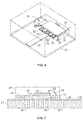
- Figure 6 is a perspective view of a circuit board layout in accordance with another embodiment of the invention for an MLP package.
- Figure 7 is an elevational cross-sectional view of an MLP package mounted to a circuit board in accordance with another embodiment of the invention.
- Various embodiments of the invention provide a connection arrangement, and more particularly, wide-band transitions for use with micro lead frame plastic (MLP) packages, including millimeter-wave MLP packages. These packages also are referred to as Quad Flat No-Lead (QFN) packages.
- MLP micro lead frame plastic
- QFN Quad Flat No-Lead
- the various embodiments include (i) matching circuits or arrangements that are either on a circuit board to which the MLP package is connected to, or on the lead frame itself, and (ii) a lead frame configuration to compensate for bond wire inductance.
- two pads, and specifically, two metal grounding pads on a motherboard connect paddle grounds to leads around an RF pad in a coplanar configuration.
- This arrangement provides a continuity of ground between the RF signal of the chip (e.g., integrated circuit (IC) chip) within the MLP package and the RF signal on the motherboard (e.g., RF board) to which the MLP package with chip is mounted.
- IC integrated circuit
- various embodiments of the present invention provide a connection arrangement for mounting a chip within an MLP package 20 having a plurality of leads 22 (e.g., copper leads).
- leads 22 e.g., copper leads.
- the size and shape of the MLP package 20 may be modified as desired or needed, for example, based on the size and shape of the chip to be mounted therein or the particular application or system in which the MLP package 20 is to be used.
- the number and positioning of the leads 22 provided may be modified as desired or needed, for example, based on the chip to be mounted within the MLP package 20.
- a connection arrangement is provided for an MLP package 20 that is to be mounted to a circuit board, such as, for example, a motherboard 24.
- a circuit board such as, for example, a motherboard 24.
- two ground pads 26 such as, for example, copper pads on the motherboard 24, are connected to a paddle 28 (e.g., copper plate), sometimes referred to as a ground paddle, through a ground pad 44 (shown more clearly in Figure 3).
- the paddle 28 may be mounted, for example, on top of the ground pad 44 using a soldering process.
- a plurality of vias 30 may be provided through the motherboard 24, for example, under the ground pad 44, to provide a common ground between the paddle 28 and the ground plane of the motherboard 24.
- the vias 30 may be hollow and metal plated or may be metal filled.
- the vias 30 also may provide a heat conduction path, for example, for heat generated in the MLP package 20 by and integrated circuit (IC) chip.
- IC integrated circuit
- the ground pads 26 and paddle 28 may be constructed of any suitable material and configured in any suitable manner to provide a grounding connection, such as, for example, with copper traces. It should be noted that the number and size of the vias 30 may be modified as desired or needed, for example, based on the size and shape of the paddle 28.
- the ground pads 26 connect two of the leads 22 through the paddle 28 and the vias 30 to the motherboard 24 to provide a continuity of ground. In various embodiments, the ground pads 26 may be connected or integrated with the paddle 28 on the motherboard 24 in any suitable manner such that a continuous of ground is provided.
- An RF line 32 (e.g., copper trace, microstrip line, etc.) or other RF circuit extends from an edge 34 of the motherboard 24 to a coplanar section 36 defined by the RF line 32 and the grounding pads 26. Further, the RF line 32 is connected to a chip 40 within the MLP package 20 through a lead 22 of the MLP package 20 using a bond wire 35 as shown more clearly in Figures 2 and 4. As shown in Figures 4 and 7, the chip 40 (e.g., GaAs IC, SiGe IC or CMOS IC) may be mounted to the paddle 28 in any manner as is known. A die coating 42 also may be provided to the chip 40 to protect the chip, for example, from the environment. Additionally, the paddle 28 is shown mounted to the ground pad 44 of the motherboard 24 using, for example, a soldering process. It should be noted that the motherboard 24 may be constructed of any suitable material or substrate.
- the shape and size of the ground pads 26 and the space provided by a gap 38 between the RF line 32 and each of the ground pads 26 is configured such that a capacitance generated at the coplanar section 36 generally matches the inductance created by the bond wires 35 (shown in Figures 4 and 7).
- a gap 38 of about 4 mils may be provided to provide a very good impedance match over a 30 GHz frequency band.
- a continuous ground is provided between an RF signal on the chip 40 and an RF signal on the motherboard 24.
- the connection of the ground pads 26 directly to the paddle 28 provides this continuity of ground (i.e., a continuous ground path) from the RF line 32 to the ground on the motherboard 24, from the ground pads 26 to the paddle 28, and through the vias 30.
- the coplanar configuration of the RF line 32 and the ground pads 26 creates a capacitance to match the inductance generated by the wire bonds 35 in the MLP package 20.
- the shape and arrangement of the RF line 32 and ground pads 26 in the coplanar section 36, and the size of the gap 38 between the RF line 32 and the ground pads 26 in the coplanar section 36 are configured as described herein to provide the matching.
- various embodiments of the present invention provide a chip-package-motherboard transition, and more particularly, a grounding arrangement and matching configuration using a coplanar section allowing for improved operation of MLP packages, and specifically, plastic MLP packages, at higher frequency ranges.
- the configuration compensates for wire bond discontinuities by providing a continuous ground between the RF line on the chip mounted in the MLP package and the RF line on the motherboard to which the MLP package is mounted. Improved scattering parameters of the transition between motherboard and MLP package, and reduced insertion losses are thereby provided. Further, constant power output at different frequency ranges is also provided.
- an MLP package may be provided that can be used for applications at millimeter-wave frequencies.
- the various embodiments of the present invention may be implemented to construct a 24 GHz MLP package for ultra-wideband frequency systems.
- MLP packages constructed according to the various embodiments of the invention can be used in different applications, for example in opto-electrical systems.
Abstract
Description
- This invention relates generally to micro lead frame plastic (MLP) packages, and more particularly, to a connection arrangement for MLP packages.
- At RF, microwave and millimeter-wave frequencies, plastic packages are preferred because of the low cost and ease of manufacturing. For example, lead frames are much lower in cost compared to substrates used in Ball Grid Array packages. However, as the operating frequency increases, the effect of the package on the component/circuit overall RF performance becomes increasingly important. In addition to good electrical characteristics, when designing a package, it is also important to consider thermal dissipation paths, space requirements or limitations, environmental protection and component reliability.
- The use of plastic packages is currently limited to low frequency applications, for example, applications with a maximum frequency of about 5 GHz. This is due mainly to the parasitics (e.g., large inductance) associated with bond wire discontinuity of the chip-package-motherboard transition. These parasitics are particularly severe at higher frequencies, such as, for example, at 24 GHz. The parasitics are also caused by the use of a paddle and ground pads that are not connected and thereby fail to provide a continuity of ground, particularly at the higher frequencies. These parasitics result in high insertion loss, poor impedance matching and a large response over the required frequency band. The RF behavior of the chip-package-motherboard transition also results in a large power drop off with frequency.
- The parasitic effects are sometimes overcome by including additional matching stubs on, for example, the Monolithic Microwave Integrated Circuit (MMIC) chip itself. However, as the space on the chip is often very limited, this on-chip matching can be complex and can be very expensive to implement. Moreover, using the matching stubs, the frequency bandwidth is very limited, making these configurations unacceptable for ultra broadband systems such as High Resolution Radar (HRR). Other solutions are also known and include using the parasitics for matching the amplifiers on the chip. However, these solutions also can be difficult to implement.
- Flip-chip versions of MLP packages are also known for addressing the operating frequency problems. In these packages, a bumped die is flipped onto a lead frame paddle and then molded using a standard plastic package assembly process. Flip chip designs reduce signal inductance because the interconnect is much shorter when compared to a bond wire (e.g., 0.1 mm versus 1 mm). However, the manufacturing processes for such flip chip processes may not be satisfactory for mass production in large quantities.
- Thus, known MLP packages either do not operate satisfactorily at higher frequencies or are complex and expensive to implement.
- According to an aspect of the present invention there is provided a connection arrangement for a micro lead frame plastic (MLP) package is provided that includes a paddle configured to be connected to a circuit board and a first ground pad and a second ground pad each connected to the paddle. The first and second ground pads together with the paddle are configured to provide a continuous of ground between the circuit board and a chip mounted to the paddle.
- According to another aspect of the present invention there is provided a micro lead frame plastic (MLP) package board is provided that includes a paddle configured to be grounded using a plurality of vias, an RF circuit, and a first ground pad and a second ground pad connected to the paddle. The first and second ground pads together with the paddle are configured to provide a continuous ground path between the RF circuit and a chip mounted to the paddle.
- According to a further aspect of the present invention there is provided a method of connecting a micro lead frame plastic (MLP) package to a circuit board is provided. The method includes providing a paddle on the circuit board and configuring a first ground pad and a second ground pad of the circuit board to connect to the paddle to provide a continuous ground between the circuit board and a chip mounted to the paddle.
- Figure 1 is a schematic block diagram of a micro lead frame (MLP) package in connection with which various embodiments of the present invention may be implemented;
- Figure 2 is a perspective view of an MLP package mounted to a circuit board in accordance with an embodiment of the invention;
- Figure 3 is a perspective view of a circuit board layout in accordance with an embodiment of the invention for an MLP package;
- Figure 4 is an elevational cross-sectional view of an MLP package mounted to a circuit board in accordance with an embodiment of the invention;
- Figure 5 is a schematic plan view of an MLP package mounted to a circuit board in accordance with an embodiment of the invention;
- Figure 6 is a perspective view of a circuit board layout in accordance with another embodiment of the invention for an MLP package; and
- Figure 7 is an elevational cross-sectional view of an MLP package mounted to a circuit board in accordance with another embodiment of the invention.
- Various embodiments of the invention provide a connection arrangement, and more particularly, wide-band transitions for use with micro lead frame plastic (MLP) packages, including millimeter-wave MLP packages. These packages also are referred to as Quad Flat No-Lead (QFN) packages. The various embodiments include (i) matching circuits or arrangements that are either on a circuit board to which the MLP package is connected to, or on the lead frame itself, and (ii) a lead frame configuration to compensate for bond wire inductance. In general, and as described in more detail herein, two pads, and specifically, two metal grounding pads on a motherboard connect paddle grounds to leads around an RF pad in a coplanar configuration. This arrangement provides a continuity of ground between the RF signal of the chip (e.g., integrated circuit (IC) chip) within the MLP package and the RF signal on the motherboard (e.g., RF board) to which the MLP package with chip is mounted.
- More particularly, and as shown in Figure 1, various embodiments of the present invention provide a connection arrangement for mounting a chip within an
MLP package 20 having a plurality of leads 22 (e.g., copper leads). It should be noted that the size and shape of theMLP package 20 may be modified as desired or needed, for example, based on the size and shape of the chip to be mounted therein or the particular application or system in which theMLP package 20 is to be used. Additionally, the number and positioning of theleads 22 provided may be modified as desired or needed, for example, based on the chip to be mounted within theMLP package 20. - Specifically, and as shown in Figures 2 and 3, in an exemplary embodiment, a connection arrangement is provided for an
MLP package 20 that is to be mounted to a circuit board, such as, for example, amotherboard 24. In this embodiment, two ground pads 26 (shown more clearly in Figure 3), such as, for example, copper pads on themotherboard 24, are connected to a paddle 28 (e.g., copper plate), sometimes referred to as a ground paddle, through a ground pad 44 (shown more clearly in Figure 3). Thus, thepaddle 28 may be mounted, for example, on top of theground pad 44 using a soldering process. A plurality of vias 30 (e.g., copper connections) may be provided through themotherboard 24, for example, under theground pad 44, to provide a common ground between thepaddle 28 and the ground plane of themotherboard 24. Thevias 30 may be hollow and metal plated or may be metal filled. Thevias 30 also may provide a heat conduction path, for example, for heat generated in theMLP package 20 by and integrated circuit (IC) chip. - The
ground pads 26 andpaddle 28 may be constructed of any suitable material and configured in any suitable manner to provide a grounding connection, such as, for example, with copper traces. It should be noted that the number and size of thevias 30 may be modified as desired or needed, for example, based on the size and shape of thepaddle 28. Theground pads 26 connect two of theleads 22 through thepaddle 28 and thevias 30 to themotherboard 24 to provide a continuity of ground. In various embodiments, theground pads 26 may be connected or integrated with thepaddle 28 on themotherboard 24 in any suitable manner such that a continuous of ground is provided. - It should be noted that only a portion of the
MLP package 20 is shown in Figures 2 and 3. Thus,additional leads 22, etc. may be provided as part of theMLP package 20. - An RF line 32 (e.g., copper trace, microstrip line, etc.) or other RF circuit extends from an
edge 34 of themotherboard 24 to acoplanar section 36 defined by theRF line 32 and thegrounding pads 26. Further, theRF line 32 is connected to achip 40 within theMLP package 20 through alead 22 of theMLP package 20 using abond wire 35 as shown more clearly in Figures 2 and 4. As shown in Figures 4 and 7, the chip 40 (e.g., GaAs IC, SiGe IC or CMOS IC) may be mounted to thepaddle 28 in any manner as is known. Adie coating 42 also may be provided to thechip 40 to protect the chip, for example, from the environment. Additionally, thepaddle 28 is shown mounted to theground pad 44 of themotherboard 24 using, for example, a soldering process. It should be noted that themotherboard 24 may be constructed of any suitable material or substrate. - Referring again to Figure 3, the shape and size of the
ground pads 26 and the space provided by a gap 38 between theRF line 32 and each of theground pads 26 is configured such that a capacitance generated at thecoplanar section 36 generally matches the inductance created by the bond wires 35 (shown in Figures 4 and 7). For example, a gap 38 of about 4 mils may be provided to provide a very good impedance match over a 30 GHz frequency band. - In another embodiment of the invention as shown in Figures 6 and 7, instead of providing a chip-package-board interconnect on the
motherboard 24 as shown in Figures 2 through 5, a connection only to the lead frame (e.g., directly to the leads 22) is provided. This configuration is similar to that shown in Figures 2 through 5, however, in this embodiment, theleads 22 are connected directly to thepaddle 28 such that no gap 46 (as shown in Figure 4) is provided between theleads 22 and thepaddle 28. However, in this embodiment, there is agap 65 between theRF line 32 and theground pad 44. - In operation, a continuous ground is provided between an RF signal on the
chip 40 and an RF signal on themotherboard 24. Specifically, the connection of theground pads 26 directly to thepaddle 28 provides this continuity of ground (i.e., a continuous ground path) from theRF line 32 to the ground on themotherboard 24, from theground pads 26 to thepaddle 28, and through thevias 30. Further, the coplanar configuration of theRF line 32 and theground pads 26 creates a capacitance to match the inductance generated by thewire bonds 35 in theMLP package 20. The shape and arrangement of theRF line 32 andground pads 26 in thecoplanar section 36, and the size of the gap 38 between theRF line 32 and theground pads 26 in thecoplanar section 36 are configured as described herein to provide the matching. - Thus, various embodiments of the present invention provide a chip-package-motherboard transition, and more particularly, a grounding arrangement and matching configuration using a coplanar section allowing for improved operation of MLP packages, and specifically, plastic MLP packages, at higher frequency ranges. The configuration compensates for wire bond discontinuities by providing a continuous ground between the RF line on the chip mounted in the MLP package and the RF line on the motherboard to which the MLP package is mounted. Improved scattering parameters of the transition between motherboard and MLP package, and reduced insertion losses are thereby provided. Further, constant power output at different frequency ranges is also provided.
- Using various embodiments of the invention, an MLP package may be provided that can be used for applications at millimeter-wave frequencies. For example, the various embodiments of the present invention may be implemented to construct a 24 GHz MLP package for ultra-wideband frequency systems. Further, because the bandwidth of these transitions is very wide, MLP packages constructed according to the various embodiments of the invention can be used in different applications, for example in opto-electrical systems.
Claims (20)
- A connection arrangement for a micro lead frame plastic (MLP) package (20), the connection arrangement comprising:a paddle (28) configured to be connected to a circuit board (24); anda first ground pad (26) and a second ground pad (26) each connected to the paddle (28) and together with the paddle (28) configured to a continuous ground between the circuit board (24) and a chip (40) mounted to the paddle (28).
- A connection arrangement in accordance with claim 1 further comprising an RF line (32) on the circuit board (24) and an RF line on the chip (40), and wherein the continuous ground is provided between the RF line (32) on the circuit board (24) and the RF line on the chip (40).
- A connection arrangement in accordance with claim 1 or 2 further comprising a plurality of leads (22) with at least a first lead configured to connect to the first ground pad (26) and at least a second lead configured to connect to the second ground pad (26).
- A connection arrangement in accordance with claim 1 further comprising an RF line (32) on the circuit board (24) and wherein the RF line (32) and first and second ground pads (26, 26) are arranged in a coplanar configuration.
- A connection arrangement in accordance with claim 1 further comprising an RF line (32) on the circuit board (24) and at least one wire bond (35) to connect a chip (40) to the circuit board (24), and wherein the RF line (32) and first and second ground pads (26, 26) are configured to generate a capacitance to match an inductance generated by the at least one wire bond (35).
- A connection arrangement in accordance with claim 5 further comprising a gap (38) between each of the first and second ground pads (26, 26) and the RF line (32).
- A connection arrangement in accordance with claim 5 further comprising a gap (65) between the paddle (28) and the RF line (32).
- A connection arrangement in accordance with claim 1 further comprising a third ground pad (44) below the paddle and wherein the first and second ground pads (26, 26) are connected to the paddle (28) through the third ground pad (44).
- A connection arrangement in accordance with claim 1 wherein the first and second ground pads (26, 26) are connected to the paddle (28) via a lead from the MLP package (20).
- A connection arrangement in accordance with claim 1 wherein the first and second ground pads (26, 26) are each integrally formed on the circuit board (24) with a third ground pad (44) for connection to the paddle (28).
- A connection arrangement in accordance with claim 1 further comprising a gap (46) between the paddle (28) and a lead (22) of the MLP package (22), and wherein a wire bond (35) connects the lead to the paddle.
- A connection arrangement in accordance with claim 1 further comprising an RF line (32) on the circuit board (24) and wherein the RF line (32) and the first and second ground pads (26, 26) are configured to provide a matching circuit.
- A micro lead frame plastic (MLP) package board comprising:a paddle (28) configured to be grounded using a plurality of vias (30);an RF circuit; anda first ground pad (26) and a second ground pad (26) connected to the paddle (28) through a third ground pad (44) and together with the paddle (28) configured to provide a continuous ground path between the RF circuit and a chip (40) mounted to the paddle (28).
- An MLP package board in accordance with claim 13 wherein the RF circuit and first and second ground pads (26, 26) are configured to generate a capacitance to match an inductance generated within the MLP package (20).
- An MLP package board in accordance with claim 13 or 14 further comprising a wire bond (35) to connect the RF circuit to a chip (40) within the MLP package (20).
- An MLP package board in accordance with claim 15 wherein the RF circuit and first and second ground pads (26, 26) are configured to generate a capacitance to match an inductance generated by the wire bond (35).
- An MLP package board in accordance with any of claims 13 to 16 wherein the RF circuit and first and second ground pads (26, 26) are configured in a coplanar arrangement.
- An MLP package board in accordance with claim 13 wherein the MLP package (20) comprises leads (22) and the ground pads are connected to the leads via a lead frame of the MLP package (20).
- A method of connecting a micro lead frame plastic (MLP) package (20) to a circuit board (24), the method comprising:providing a paddle (28) on the circuit board (24); andconfiguring a first ground pad (26) and a second ground pad (26) of the circuit board to connect to the paddle (28) to provide a continuous ground between the circuit board (24) and a chip (40) mounted to the paddle (28).
- A method in accordance with claim 19 further comprising configuring an RF circuit formed on the circuit board (24) in a coplanar arrangement with the first and second ground pads (26, 26).
Applications Claiming Priority (1)
| Application Number | Priority Date | Filing Date | Title |
|---|---|---|---|
| US10/999,591 US7211887B2 (en) | 2004-11-30 | 2004-11-30 | connection arrangement for micro lead frame plastic packages |
Publications (2)
| Publication Number | Publication Date |
|---|---|
| EP1675178A2 true EP1675178A2 (en) | 2006-06-28 |
| EP1675178A3 EP1675178A3 (en) | 2008-05-28 |
Family
ID=36353337
Family Applications (1)
| Application Number | Title | Priority Date | Filing Date |
|---|---|---|---|
| EP05111431A Withdrawn EP1675178A3 (en) | 2004-11-30 | 2005-11-29 | Connection arrangement for micro lead frame plastic packages |
Country Status (4)
| Country | Link |
|---|---|
| US (1) | US7211887B2 (en) |
| EP (1) | EP1675178A3 (en) |
| JP (1) | JP2006157011A (en) |
| CN (1) | CN1797760A (en) |
Families Citing this family (12)
| Publication number | Priority date | Publication date | Assignee | Title |
|---|---|---|---|---|
| US8399968B2 (en) * | 2005-11-18 | 2013-03-19 | Stats Chippac Ltd. | Non-leaded integrated circuit package system |
| TWI302813B (en) * | 2006-01-11 | 2008-11-01 | Via Tech Inc | Circuit board and electronic assembly |
| US8003443B2 (en) | 2006-03-10 | 2011-08-23 | Stats Chippac Ltd. | Non-leaded integrated circuit package system with multiple ground sites |
| US8062934B2 (en) * | 2006-06-22 | 2011-11-22 | Stats Chippac Ltd. | Integrated circuit package system with ground bonds |
| TWI315567B (en) * | 2006-11-10 | 2009-10-01 | Via Tech Inc | Electronic assembly and circuit board |
| US7768105B2 (en) * | 2007-01-24 | 2010-08-03 | Fairchild Semiconductor Corporation | Pre-molded clip structure |
| US7755173B2 (en) * | 2007-06-26 | 2010-07-13 | M/A-Com Technology Solutions Holdings, Inc. | Series-shunt switch with thermal terminal |
| US8664038B2 (en) * | 2008-12-04 | 2014-03-04 | Stats Chippac Ltd. | Integrated circuit packaging system with stacked paddle and method of manufacture thereof |
| US20110115063A1 (en) * | 2009-11-18 | 2011-05-19 | Entropic Communications, Inc. | Integrated Circuit Packaging with Split Paddle |
| US10271448B2 (en) * | 2012-08-06 | 2019-04-23 | Investar Corporation | Thin leadframe QFN package design of RF front-ends for mobile wireless communication |
| US9515032B1 (en) | 2015-08-13 | 2016-12-06 | Win Semiconductors Corp. | High-frequency package |
| US10128170B2 (en) | 2017-01-09 | 2018-11-13 | Silanna Asia Pte Ltd | Conductive clip connection arrangements for semiconductor packages |
Citations (9)
| Publication number | Priority date | Publication date | Assignee | Title |
|---|---|---|---|---|
| US4172261A (en) * | 1977-01-10 | 1979-10-23 | Nippon Electric Co., Ltd. | Semiconductor device having a highly air-tight package |
| US4975761A (en) * | 1989-09-05 | 1990-12-04 | Advanced Micro Devices, Inc. | High performance plastic encapsulated package for integrated circuit die |
| US5153379A (en) * | 1990-10-09 | 1992-10-06 | Motorola, Inc. | Shielded low-profile electronic component assembly |
| WO1994017552A1 (en) * | 1993-01-29 | 1994-08-04 | Anadigics, Inc. | Plastic packages for microwave frequency applications |
| US5612853A (en) * | 1993-07-12 | 1997-03-18 | Electronics And Telecommunications Research Institute | Package for a power semiconductor device |
| GB2329068A (en) * | 1997-09-08 | 1999-03-10 | Hewlett Packard Co | A vertical interconnect package for electronic components |
| US20020166689A1 (en) * | 2001-03-27 | 2002-11-14 | Maraki Maetani | High frequency semiconductor device housing package and mounting structure for mounting the same |
| US20030209784A1 (en) * | 2002-05-09 | 2003-11-13 | Schmitz Norbert A. | Package for integrated circuit with internal matching |
| WO2004075336A1 (en) * | 2003-02-21 | 2004-09-02 | Matsushita Electric Industrial Co., Ltd. | High frequency circuit |
Family Cites Families (5)
| Publication number | Priority date | Publication date | Assignee | Title |
|---|---|---|---|---|
| US5422664A (en) * | 1993-06-25 | 1995-06-06 | Xerox Corporation | Method and apparatus for maintaining constant drop size mass in thermal ink jet printers |
| US6791166B1 (en) * | 2001-04-09 | 2004-09-14 | Amkor Technology, Inc. | Stackable lead frame package using exposed internal lead traces |
| US7026664B2 (en) * | 2003-04-24 | 2006-04-11 | Power-One, Inc. | DC-DC converter implemented in a land grid array package |
| TWI249832B (en) * | 2003-11-10 | 2006-02-21 | Siliconware Precision Industries Co Ltd | Lead frame and semiconductor package with the lead frame |
| US7261793B2 (en) * | 2004-08-13 | 2007-08-28 | Hewlett-Packard Development Company, L.P. | System and method for low temperature plasma-enhanced bonding |
-
2004
- 2004-11-30 US US10/999,591 patent/US7211887B2/en not_active Expired - Fee Related
-
2005
- 2005-11-28 JP JP2005341592A patent/JP2006157011A/en active Pending
- 2005-11-29 EP EP05111431A patent/EP1675178A3/en not_active Withdrawn
- 2005-11-30 CN CNA2005101270723A patent/CN1797760A/en active Pending
Patent Citations (9)
| Publication number | Priority date | Publication date | Assignee | Title |
|---|---|---|---|---|
| US4172261A (en) * | 1977-01-10 | 1979-10-23 | Nippon Electric Co., Ltd. | Semiconductor device having a highly air-tight package |
| US4975761A (en) * | 1989-09-05 | 1990-12-04 | Advanced Micro Devices, Inc. | High performance plastic encapsulated package for integrated circuit die |
| US5153379A (en) * | 1990-10-09 | 1992-10-06 | Motorola, Inc. | Shielded low-profile electronic component assembly |
| WO1994017552A1 (en) * | 1993-01-29 | 1994-08-04 | Anadigics, Inc. | Plastic packages for microwave frequency applications |
| US5612853A (en) * | 1993-07-12 | 1997-03-18 | Electronics And Telecommunications Research Institute | Package for a power semiconductor device |
| GB2329068A (en) * | 1997-09-08 | 1999-03-10 | Hewlett Packard Co | A vertical interconnect package for electronic components |
| US20020166689A1 (en) * | 2001-03-27 | 2002-11-14 | Maraki Maetani | High frequency semiconductor device housing package and mounting structure for mounting the same |
| US20030209784A1 (en) * | 2002-05-09 | 2003-11-13 | Schmitz Norbert A. | Package for integrated circuit with internal matching |
| WO2004075336A1 (en) * | 2003-02-21 | 2004-09-02 | Matsushita Electric Industrial Co., Ltd. | High frequency circuit |
Also Published As
| Publication number | Publication date |
|---|---|
| JP2006157011A (en) | 2006-06-15 |
| CN1797760A (en) | 2006-07-05 |
| US20060113646A1 (en) | 2006-06-01 |
| US7211887B2 (en) | 2007-05-01 |
| EP1675178A3 (en) | 2008-05-28 |
Similar Documents
| Publication | Publication Date | Title |
|---|---|---|
| EP1675178A2 (en) | Connection arrangement for micro lead frame plastic packages | |
| US7911066B2 (en) | Through-chip via interconnects for stacked integrated circuit structures | |
| US8035203B2 (en) | Radio frequency over-molded leadframe package | |
| US20030198032A1 (en) | Integrated circuit assembly and method for making same | |
| KR20010110421A (en) | Multiple chip module with integrated rf capabilities | |
| KR20120035394A (en) | Apparatus for system-on-package using vertical transmission line transition and land grid array connection | |
| CN110556365B (en) | Matching circuit for integrated circuit wafer | |
| US6130478A (en) | Polymer stud grid array for microwave circuit arrangements | |
| US6507110B1 (en) | Microwave device and method for making same | |
| US6414387B1 (en) | Semiconductor device including a chip having high-frequency circuit blocks | |
| US6998292B2 (en) | Apparatus and method for inter-chip or chip-to-substrate connection with a sub-carrier | |
| KR100270954B1 (en) | Wire-bond free input/output interface for gaas ics with means of determining known good die | |
| US20010048155A1 (en) | Interchangeable bond-wire interconnects | |
| Namaki et al. | A tunable macro-modeling method for signal transition in mm-wave flip-chip technology | |
| KR20040063784A (en) | Semiconductor apparatus | |
| Mahon et al. | A surface mount 45 to 90 GHz low noise amplifier using novel hot-via interconnection | |
| JP3998562B2 (en) | Semiconductor device | |
| US7105924B2 (en) | Integrated circuit housing | |
| JPH0936617A (en) | High frequency module | |
| JP3933601B2 (en) | High frequency integrated circuit package and electronic device | |
| Bessemoulin et al. | Demonstration of reproducible Millimeter-wave SMT Chip Scale Package using Hot-via MMICs and Plastic BGA Encapsulation | |
| JP2007235149A (en) | Semiconductor device and electronic device | |
| CN116153859A (en) | Wafer level packaging method of monolithic microwave integrated circuit | |
| JP2001284490A (en) | Grounding structure for high-frequency wave | |
| TWI528507B (en) | Chip package structure |
Legal Events
| Date | Code | Title | Description |
|---|---|---|---|
| PUAI | Public reference made under article 153(3) epc to a published international application that has entered the european phase |
Free format text: ORIGINAL CODE: 0009012 |
|
| AK | Designated contracting states |
Kind code of ref document: A2 Designated state(s): AT BE BG CH CY CZ DE DK EE ES FI FR GB GR HU IE IS IT LI LT LU LV MC NL PL PT RO SE SI SK TR |
|
| AX | Request for extension of the european patent |
Extension state: AL BA HR MK YU |
|
| PUAL | Search report despatched |
Free format text: ORIGINAL CODE: 0009013 |
|
| AK | Designated contracting states |
Kind code of ref document: A3 Designated state(s): AT BE BG CH CY CZ DE DK EE ES FI FR GB GR HU IE IS IT LI LT LU LV MC NL PL PT RO SE SI SK TR |
|
| AX | Request for extension of the european patent |
Extension state: AL BA HR MK YU |
|
| AKX | Designation fees paid | ||
| REG | Reference to a national code |
Ref country code: DE Ref legal event code: 8566 |
|
| RAP1 | Party data changed (applicant data changed or rights of an application transferred) |
Owner name: COBHAM DEFENSE ELECTRONIC SYSTEMS CORPORATION |
|
| STAA | Information on the status of an ep patent application or granted ep patent |
Free format text: STATUS: THE APPLICATION IS DEEMED TO BE WITHDRAWN |
|
| 18D | Application deemed to be withdrawn |
Effective date: 20081201 |