EP1684342A2 - Method for manufacturing a semiconductor memory device - Google Patents
Method for manufacturing a semiconductor memory device Download PDFInfo
- Publication number
- EP1684342A2 EP1684342A2 EP06075802A EP06075802A EP1684342A2 EP 1684342 A2 EP1684342 A2 EP 1684342A2 EP 06075802 A EP06075802 A EP 06075802A EP 06075802 A EP06075802 A EP 06075802A EP 1684342 A2 EP1684342 A2 EP 1684342A2
- Authority
- EP
- European Patent Office
- Prior art keywords
- landing pad
- layer
- semiconductor substrate
- ild
- film
- Prior art date
- Legal status (The legal status is an assumption and is not a legal conclusion. Google has not performed a legal analysis and makes no representation as to the accuracy of the status listed.)
- Granted
Links
Images


Classifications
-
- H—ELECTRICITY
- H10—SEMICONDUCTOR DEVICES; ELECTRIC SOLID-STATE DEVICES NOT OTHERWISE PROVIDED FOR
- H10B—ELECTRONIC MEMORY DEVICES
- H10B12/00—Dynamic random access memory [DRAM] devices
- H10B12/01—Manufacture or treatment
- H10B12/02—Manufacture or treatment for one transistor one-capacitor [1T-1C] memory cells
- H10B12/03—Making the capacitor or connections thereto
- H10B12/033—Making the capacitor or connections thereto the capacitor extending over the transistor
- H10B12/0335—Making a connection between the transistor and the capacitor, e.g. plug
-
- H—ELECTRICITY
- H10—SEMICONDUCTOR DEVICES; ELECTRIC SOLID-STATE DEVICES NOT OTHERWISE PROVIDED FOR
- H10B—ELECTRONIC MEMORY DEVICES
- H10B12/00—Dynamic random access memory [DRAM] devices
- H10B12/01—Manufacture or treatment
- H10B12/09—Manufacture or treatment with simultaneous manufacture of the peripheral circuit region and memory cells
-
- H—ELECTRICITY
- H10—SEMICONDUCTOR DEVICES; ELECTRIC SOLID-STATE DEVICES NOT OTHERWISE PROVIDED FOR
- H10B—ELECTRONIC MEMORY DEVICES
- H10B12/00—Dynamic random access memory [DRAM] devices
- H10B12/30—DRAM devices comprising one-transistor - one-capacitor [1T-1C] memory cells
- H10B12/48—Data lines or contacts therefor
- H10B12/485—Bit line contacts
-
- H—ELECTRICITY
- H01—ELECTRIC ELEMENTS
- H01L—SEMICONDUCTOR DEVICES NOT COVERED BY CLASS H10
- H01L27/00—Devices consisting of a plurality of semiconductor or other solid-state components formed in or on a common substrate
- H01L27/02—Devices consisting of a plurality of semiconductor or other solid-state components formed in or on a common substrate including semiconductor components specially adapted for rectifying, oscillating, amplifying or switching and having at least one potential-jump barrier or surface barrier; including integrated passive circuit elements with at least one potential-jump barrier or surface barrier
- H01L27/04—Devices consisting of a plurality of semiconductor or other solid-state components formed in or on a common substrate including semiconductor components specially adapted for rectifying, oscillating, amplifying or switching and having at least one potential-jump barrier or surface barrier; including integrated passive circuit elements with at least one potential-jump barrier or surface barrier the substrate being a semiconductor body
- H01L27/10—Devices consisting of a plurality of semiconductor or other solid-state components formed in or on a common substrate including semiconductor components specially adapted for rectifying, oscillating, amplifying or switching and having at least one potential-jump barrier or surface barrier; including integrated passive circuit elements with at least one potential-jump barrier or surface barrier the substrate being a semiconductor body including a plurality of individual components in a repetitive configuration
- H01L27/105—Devices consisting of a plurality of semiconductor or other solid-state components formed in or on a common substrate including semiconductor components specially adapted for rectifying, oscillating, amplifying or switching and having at least one potential-jump barrier or surface barrier; including integrated passive circuit elements with at least one potential-jump barrier or surface barrier the substrate being a semiconductor body including a plurality of individual components in a repetitive configuration including field-effect components
-
- H—ELECTRICITY
- H10—SEMICONDUCTOR DEVICES; ELECTRIC SOLID-STATE DEVICES NOT OTHERWISE PROVIDED FOR
- H10B—ELECTRONIC MEMORY DEVICES
- H10B12/00—Dynamic random access memory [DRAM] devices
- H10B12/30—DRAM devices comprising one-transistor - one-capacitor [1T-1C] memory cells
- H10B12/31—DRAM devices comprising one-transistor - one-capacitor [1T-1C] memory cells having a storage electrode stacked over the transistor
- H10B12/315—DRAM devices comprising one-transistor - one-capacitor [1T-1C] memory cells having a storage electrode stacked over the transistor with the capacitor higher than a bit line
Definitions
- the present invention relates to a semiconductor memory device manufacturing method, and more particularly, to a method for manufacturing a semiconductor memory device having improved contact alignment
- DRAM dynamic random access memory
- a contact in a cell array portion such as a contact for connecting a storage electrode of a capacitor to a semiconductor substrate, is usually formed between a bit line and a gate electrode line.
- a semiconductor memory device of 64M DRAM or more adopts a capacitor on bit-line (COB) structure, which results in an increase of a step difference between a cell array region and a peripheral circuit region. Accordingly, it is very difficult to secure an appropriate focus margin and form a fine pattern.
- COB capacitor on bit-line
- An aim of at least preferred embodiments of the present invention is to provide a method for manufacturing a semiconductor memory device, allowing an alignment margin for a contact.
- a method for manufacturing a semiconductor memory device comprising the steps of forming gate electrodes on a semiconductor substrate, the gate electrodes being covered with a nitride spacer. Then, a thermal oxide layer is formed on the exposed surface of the semiconductor substrate between the gate electrodes, and an etch stop layer is then formed on the entire surface of the resultant structure having the thermal oxide layer to an appropriate thickness such that the space between the gate electrodes is not buried. Then, a first interlayer dielectric (ILD) film covering the space is formed between the gate electrodes and the top of the gate electrodes, and the first ILD film is then patterned to form a landing pad hole which exposes the spacer and the etch stop layer. Then, the etch stop layer and the thermal oxide layer are removed to expose the surface of the semiconductor substrate, and then the landing pad hole is filled with a conductive material to form a contact plug, resulting in landing pads.
- ILD interlayer dielectric
- a first conductive layer is formed on the entire surface of the resultant structure having the landing pad hole, and the first conductive layer is etched until the surface of the first ILD film is exposed, to form the contact plug in the landing pad hole.
- the first conductive layer is preferably formed by a chemical mechanical polishing (CMP) method or by etching back the first conductive layer.
- the method for manufacturing the semiconductor memory device further comprises the steps of forming a second ILD film on the resultant structure having the landing pads. Then, the second ILD film is patterned to form a bit line contact hole which exposes the surface of a part of the landing pads, and a bit line contact plug is then formed in the bit line contact hole. Then, a bit line which is connected to the bit line contact plug is formed on the resultant structure having the bit line contact plug.
- the manufacturing method further comprises the steps of forming a third ILD film on the resultant structure having the bit line. Then, the third ILD film is patterned to form a storage electrode contact hole which exposes the surface of the other part of the landing pads, and a storage electrode is then formed, which is connected to the semiconductor substrate via the storage electrode contact hole and the other part of the landing pads. Then, a dielectric film is formed on the storage electrode, and then an upper electrode is formed on the dielectric layer to complete a capacitor.
- a method for manufacturing a semiconductor memory device comprising the steps of forming a gate electrode on a semiconductor substrate having a cell array region and a peripheral circuit region, the gate electrode being covered with a spacer. Then, a planarized first interlayer dielectric (ILD) film is formed on the semiconductor substrate having the gate electrode, and a second ILD film is then formed on the first ILD film. Then, a remaining preventing layer is formed on the second ILD film, and the remaining preventing layer, the second ILD film and the first ILD film are patterned in sequence to form a landing pad hole which simultaneously exposes an active region of the semiconductor substrate, and a part of the spacer in the cell array region. Then, a contact plug is formed in the landing pad hole, resulting in landing pads.
- ILD interlayer dielectric
- a method for manufacturing a semiconductor memory device comprising the steps of forming gate electrodes on a semiconductor substrate, the gate electrodes being covered with a nitride spacer. Then, a thermal oxide layer is formed on the surface of the semiconductor substrate which is exposed between the gate electrodes. Then, an etch stop layer is formed on the entire surface of the resultant structure having the thermal oxide layer to an appropriate thickness such that the space between the gate electrodes is not buried. Then, a first oxide layer is formed in the space between the gate electrodes, and then a second oxide layer is formed on the first oxide layer.
- a polysilicon layer is formed on the second oxide layer, and the polysilicon layer, the second oxide layer, the first oxide layer, the etch stop layer and the thermal oxide layer are partially etched in sequence, to form a landing pad hole which simultaneously exposes the surface of the semiconductor substrate and a part of the spacer. Then, a landing pad is formed in the landing pad hole.
- a sufficient alignment margin can be secured in the formation of a landing pad without damaging the semiconductor substrate, and the step difference in the semiconductor substrate can be minimized.
- a bit line and a storage electrode of a capacitor are connected to an active region of a semiconductor substrate via self-aligned landing pads.
- Figure 1 shows the layout of a cell array region of a semiconductor memory device manufactured by a method according to a first embodiment.
- Figure 1 shows the state where landing pads 117a and 117b are formed on a gate electrode 105 in a self-aligning manner, and the formation of a bit line thereon is completed.
- reference character "AA" represents an active region
- reference numeral 105 represents a gate electrode
- reference numeral 107 represents a spacer for capping the gate electrode 105
- reference numeral 117a represents a landing pad for connecting a storage electrode of a capacitor to a semiconductor substrate
- reference numeral 117b represents a landing pad for connecting the bit line to the semiconductor substrate.
- reference numeral 120 represents a bit line contact hole
- reference numeral 123 represents a bit line.
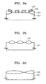
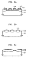
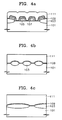
- Figures 2a, 3a to 14a are section views cut along line A-A' of Figure 1
- Figures 2b to 14b are section views cut along line B-B' of Figure 1
- Figures 2c to 14c are section views cut along line C-C' of Figure 1.
- a gate electrode 105 and a spacer 107 for capping the gate electrode 105 are formed in sequence on a semiconductor substrate 101 in which an active region and a non-active region are divided by an isolation film 103 such as a field oxide layer. Then, a source/drain (not shown) is formed in the active region between the gate electrodes 105 by an ion implantation process, thereby completing a transistor consisting of the gate electrode 105 and the source/drain.
- a thermal oxide layer (not shown) is formed on the semiconductor substrate 101 to a thickness of approximately 50-150A. If the thickness of the thermal oxide layer exceeds the above range, the thermal oxide layer should be partially etched when etching the silicon nitride layer as an etch stop layer in a subsequent step.
- a field oxide layer may be etched together, so that the thermal oxide layer can be grown to a minimum thickness.
- an etch stop layer 109 made of silicon nitride is formed on the entire surface of the resultant structure having the thermal oxide layer to a thickness of at least 100A.
- the etch stop layer 109 is formed to the optimum thickness, to at least 100A, such that the space between the gate electrodes 105 is not buried.
- a first oxide layer 111 is formed on the resultant structure having the etch stop layer 109 to a thickness that is sufficient to completely bury the space between the gate electrodes 105.
- the first oxide layer 111 is planarized by a chemical mechanical polishing (CMP) process, using the etch stop layer 109 as an etching end point, thereby resulting in a planarized first oxide layer 111a.
- CMP chemical mechanical polishing
- a second oxide layer 113 e.g., an oxide layer formed by chemical vapor deposition (CVD) is formed on the planarized first oxide layer 111a to a predetermined thickness, to form a first interlayer dielectric (ILD) film 114 consisting of the first oxide layer 111a and the second oxide layer 113.
- the thickness of the second oxide layer 113 is controlled such that the thickness of the first ILD film 114 is the same as that of landing pads to be formed in a subsequent step.
- the first ILD film 114 and the etch stop layer 109 are patterned by photolithography, to form a first ILD film pattern 114a.
- a landing pad hole 116 is also formed, which exposes the spacer 107 covering the gate electrode 105 and the etch stop layer 109 formed on the semiconductor substrate 101.
- the exposed thermal oxide layer (not shown) is removed by dry or wet etching so that the surface of the semiconductor substrate 101 is exposed by the landing pad hole 116.
- a first conductive layer 117 e.g., an impurity-doped polysilicon layer, is formed in the landing pad hole 116 and on the first ILD pattern 114a.
- the first conductive layer 117 is etched by CMP or an etch back process until the surface of the first ILD pattern 114a is exposed, thereby forming landing pads 117a and 117b in the landing pad holes 116.
- a conductive material e.g., impurity-doped polysilicon
- the landing pad hole 116 is first formed, and then the first conductive layer 117 is deposited and planarized, resulting in self-aligned landing pads 117a and 117b.
- the first ILD film 114 made of an oxide having a high etching selectivity to the semiconductor substrate 101 is etched so that damage to the semiconductor substrate can be prevented even though it may be mis-aligned. Also, when etching the first conductive layer 117 by a CMP process to form the landing pads 117a and 117b, the surface of the semiconductor substrate is precisely planarized after the landing pads 117a and 117b are formed. Thus, when forming an ILD film on the surface of the semiconductor substrate, the ILD film can be formed by only a deposition step, without a need for a step of reflowing insulation material such as borophosphosilicate glass (BPSG) or an additional planarizing step.
- BPSG borophosphosilicate glass
- a second ILD film 119 e.g., an oxide layer such as BPSG, is deposited to a thickness of approximately 500 ⁇ 3,000A on the resultant structure having the landing pads 117a and 117b.
- the landing pads 117a and 117b are formed by the above-described patterning method, there is no need for an extra step for planarizing the insulation film.
- the second ILD film 119 is patterned to form a second ILD film pattern 119a having a bit line contact hole 120 which exposes the landing pad 117b connected to the drain in the cell array region of the semiconductor substrate 101, and a landing pad connected to the active region and a landing pad connected to the gate electrode in the peripheral circuit region.
- a second conductive layer e.g., an impurity-doped polysilicon layer, is formed on the entire surface of the resultant structure, to a thickness sufficient to bury the bit line contact hole 120.
- the second conductive layer 121 is etched by a CMP process or an etch back process until the second ILD film pattern 119a is exposed, thereby forming a bit line contact plug 121a.
- a third conductive layer e.g., an amorphous tungsten silicide (WSi x ) layer, is formed by a CVD process or a physical vapor deposition method, and then patterned to form a bit line 123.
- WSi x amorphous tungsten silicide
- the reason for depositing the tungsten silicide forming the bit line 123 in an amorphous state is to free the same from stress in a subsequent thermal process. That is, if a crystallized tungsten silicide is deposited, lifting occurs in the interface with the upper layer due to stress in a high-temperature thermal process performed at 600°C or higher.
- a third ILD film 125 is formed on the entire surface of the semiconductor substrate 101 having the bit line 123.
- the third ILD film 125 is formed of an oxide layer which can be deposited at a lower temperature, i.e., at 500°C or less, that is, a low-temperature oxide layer.
- the third ILD film 125 may be formed, for example, by forming an O 3 -tetraethyl ortho silicate (TEOS) undoped silicate glass (USG) layer by an atmosphere pressure chemical vapor deposition (APCVD) method.
- TEOS O 3 -tetraethyl ortho silicate
- USG undoped silicate glass
- APCVD atmosphere pressure chemical vapor deposition
- a plasma type oxide layer may be deposited on the semiconductor substrate 101 having the bit line 123 to a thickenss of 100 ⁇ 2,000A, and BPSG is then deposited on the plasma type oxide layer, and then reflowing is performed.
- the second example requires an additional planarization step since the plasma type oxide layer without flow characteristics is used.
- a good planarized layer can be formed even though the thickness of the deposited layer is 3,500A or less due to its excellent filling characteristics so that an additional process such as flowing is unnecessary.
- the amorphous tungsten silicide is crystallized via a phase shift at near 600°C, thereby increasing stress.
- the third ILD film 125 is composed of a low-temperature oxide layer which is formed at a lower temperature of 500°C, the lifting phenomenon in the interface between the tungsten silicide layer and the upper layer thereof can be prevented.
- the third ILD film 125 and the second ILD film pattern 119a are patterned to form a third ILD film pattern 125a and the second ILD film pattern 119b, resulting in a storage electrode contact hole 126 which exposes the surface of the landing pad 117a connected to the source of the transistor.
- a fourth conductive layer i.e., an impurity-doped polysilicon layer, is formed on the entire surface of the resultant structure having the storage electrode contact hole 126, and then patterned to form a storage electrode 127.
- a step difference corresponding to only the thickness of the storage electrode 127 exists on the semiconductor substrate 101.
- a dielectric film 131 and a plate electrode 133 are sequentially formed on the storage electrode 127, completing a capacitor.
- a nitride layer is formed on the storage electrode 127 prior to the formation of the dielectric layer 131.
- the resultant structure is heated to approximately 750°C under a nitrogen atmophere, and then an oxidation process is performed on the resultant structure when the temperature exceeds 750°C, thereby forming the dielectric film 131 having a nitride/oxide structure.
- the dielectric film 131 is formed by the above method, oxidation of the bit line 123 during an oxidation process can be prevented.
- a patterning method is used for forming the landing pad, and the bit line is formed after the bit line contact pad is formed so that the step difference on the semiconductor substrate can be minimized and the semiconductor substrate can be planarized by a simpler process. As a result, the step difference between the cell array region and the peripheral circuit region are decreased to the thickness of the storage electrode.
- a method capable of solving the problem of a dishing phenomenon is provided. Dishing may occur in a peripheral circuit region when the conductive layer deposited on a portion other than the inside of the landing pad hole is etched by a CMP method.
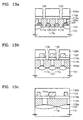
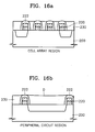
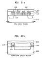
- Figures 15a and 15b through Figures 21a and 21b are section views illustrating a semiconductor memory device manufacturing method according to the second embodiment.
- Figures 15a to 21a show a cell array region
- Figures 15b to 21b show a peripheral circuit region.
- a gate electrode 220 is formed on a semiconductor substrate 200 by a shallow trench isolation (STI) method, in which an isolation region and an active region is divided.
- the gate electrode 220 may be formed to have a polycide structure consisting of a polysilicon layer and a tungsten silicide layer.
- the interval between the gate electrodes 220 is less than 0.5 ⁇ m in the cell array region while that in the peripheral circuit region may be several tens of ⁇ m.
- a spacer 222 covering the gate electrode 220 is formed using a silicon nitride layer in a subsequent step in consideration of the etching selectivity of the silicon nitride layer to an oxide layer used as an ILD film.
- a source/drain (not shown) is formed in the active region between the gate electrodes 220 in the cell array region by an ion implantation process, thereby completing a transistor consisting of the gate electrode 220 and the source/drain.
- BPSG is deposited on the resultant structure to a thickness of 4,000A or more, and then flowed at a higher temperature. Then, planarization is performed by a CMP process, using the spacer 222 as an etching end point, thereby forming a first ILD film 230.
- the gate electrodes 220 are formed with a narrower interval in the cell array region, dishing does not occur on the surface of the first ILD film 230 after the planarization using the CMP process.
- the interval between the gate electrodes 220 is comparatively wider in the peripheral circuit region, so that dishing represented by "D" in Figure 16b, occurs on the surface of the first ILD film 230 after the CMP process.
- an oxide layer is deposited to a predetermined thickness on the first ILD film 230 to form a second ILD film 240.
- dishing is reflected on the second ILD film 240 in the peripheral circuit region.
- impurity-undoped polysilicon material is deposited on the second ILD film 240 to a thickness of several hundred A, to form a remaining preventing layer 245.
- the thickness of the remaining preventing layer 245 may differ according to the degree of dishing on the second ILD film 240, however, the thickness is preferably 200 ⁇ 1,000A.
- the impurity-undoped polysilicon forming the remaining preventing layer 245 is very rapidly etched compared to the impurity-doped polysilicon. Thus, when etching back the impurity-doped polysilicon layer in a subsequent step, no residue remains in the portion in which the dishing occured.
- the remaining preventing layer 245 prevents diffused reflection of incident beams from the tungsten silicide layer of the gate electrode during a photolithography process for forming the contact, so that the deformation of a photoresist material is also prevented. Also, an increase in the contact size, caused by a poor etching selectivity between the photoresist material used for forming a contact in a subsequent step and the oxide layer forming the second ILD film 240, is prevented by the remaining preventing layer 245.
- a landing pad hole h 2 is formed by sequentially etching the remaining preventing layer 245, the second ILD film 240 and the first ILD film 230 using a general photolithography process, such that the active region of the semiconductor substrate 200 and the spacer 222 are partially exposed at the same time.
- the second ILD film 240 is etched using an equipment which provides excellent etching selectivity to the spacer 222 covering the gate electrode 220, such that the spacer 222 is protected and a short between the gate electrode 220 and the landing pad is prevented.
- a conductive layer 250 for forming a landing pad e.g., an impurity-doped polysilicon layer, is deposited on the entire surface of the resultant structure having the landing pad hole h 2 , to a thickness sufficient to completely bury the landing pad hole h 2 .
- a portion of the conductive layer 250 other than the portion formed in the landing pad hole h 2 , and the remaining preventing layer 245 are all removed by a CMP process, thereby forming a landing pad 260 in a self-align manner.
- the remaining preventing layer 245 may remain in the peripheral circuit region in which dishing occurred.
- the impurity-undoped polysilicon is removed by as much as 4-5 times faster than the impurity-doped polysilicon, the doped polysilicon material and the remaining preventing layer 245 are completely removed from all regions of the cell array region and peripheral circuit region except the landing pad 260. As a result, any remaining layer is not formed on the second ILD film 240.
- the unintended material on the ILD film, caused by the dishing can be prevented from remaining.
- Figures 22 through 28 are section views illustrating a semiconductor memory device manufactured according to the method of a third embodiment.
- a gate electrode 320 is formed on a semiconductor substrate 310 by an STI method, in which an isolation region 312 and an active region are divided.
- the gate electrode 320 is formed to have a polycide structure consisting of, e.g., a polysilicon layer and a tungsten silicide layer.
- a spacer 322 covering the gate electrode 320 is formed using a silicon nitride layer in a subsequent step in consideration of the etching selectivity of the silicon nitride layer to an oxide layer used as an ILD film.
- a source/drain (not shown) is formed in the active region between the gate electrodes 320 in the cell array region by an ion implantation process, thereby completing a transistor consisting of the gate electrode 320 and source/drain.
- a thermal oxide layer 323 is formed to a thickness of 50-150A on the semiconductor substrate 310.
- an etch stop layer 325 made of silicon nitride is formed on the entire surface of the resultant structure having the thermal oxide layer 323 to a thickness of approximately 100A.
- the etch stop layer 325 is formed to a thickness at least 100A such that the space between the gate electrodes 320 is not buried.
- a first oxide layer 327 is formed on the space between the gate electrodes 320 in the resultant structure having the etch stop layer 325.
- the distance between the gate electrodes is 0.15 ⁇ m or less.
- a material having excellent flow characteristics e.g., BPSG or spin-on glass (SOG) is first deposited on the resultant structure having the etch stop layer 325, to a thickness of approximately 1,000A, and the deposited layer is then etched at 45° angle to widen the opening between the gate electrodes 320.
- BPSG or SOG is deposited thereon to a thickness of 5,000A, and then planarized by a flowing process, thereby resulting in a BPSG layer or an SOG layer. Then, the BPSG layer or the SOG layer is planarized by a CMP process, using the etch stop layer 325 as an etching end point, thereby completing the first oxide layer 327.
- a second oxide layer 329 e.g., a P-TEOS layer capable of being deposited at a lower temperature, is deposited on the entire surface of the resultant structure having the first oxide layer 327 to a thickness of approximately 2,500A. Also, in order to prevent the entrance of the landing pad hole from being widened during a subsequent etching process for forming a landing pad hole, a polysilicon layer 331 is deposited to a thickness of approximately 500A.
- a photoresist pattern 333 is formed on the polysilicon layer 331 to define a region in which a landing pad is to be formed.
- the polysilicon layer 331, the second oxide layer 329, the first oxide layer 327, the etch stop layer 325 and the thermal oxide layer 323 are sequentially etched using the photoresist pattern 333 as a mask, thereby forming a polysilicon layer pattern 331a, a second oxide layer pattern 329a and an etch stop layer pattern 325a.
- a landing pad hole A which simultaneously exposes the surface of the semiconductor substrate 310 and the spacer 322 is formed.
- the etching process is performed under the condition for an oxide layer, so that the spacer 322 made of nitride and the surface of the semiconductor substrate 310 made of silicon are not damaged. Then, the photoresist pattern 333 is removed.
- a conductive layer e.g., an impurity-doped polysilicon layer
- a conductive layer is deposited on the resultant structure having the landing pad hole A, to a thickness sufficient to fill the landing pad hole A.
- the conductive layer and the polysilicon layer pattern 331 are etched by a CMP process, using the second oxide layer pattern 329a as an etch stop layer, thereby forming a planarized landing pad 340 in the landing pad hole A.
- a second oxide layer pattern formed in the space of each landing pad, using a P-TEOS is repeatedly formed in the cell array region, and the second oxide pattern made of P-TEOS also exists in the region other than the cell array region, so that the surface of the semiconductor substrate is accurately planarized without dishing.
- a landing pad is formed by a patterning method so that a sufficient alignment margin can be secured without damaging the semiconductor substrate. Also, after a bit line contact pad is formed, a bit line is formed thereon, so that the step difference in the semiconductor substrate is minimized and the semiconductor substrate is planarized by a simpler process. As a result, the step difference between the cell array region and the peripheral circuit region is decreased to the thickness of a storage electrode.
Abstract
Description
- The present invention relates to a semiconductor memory device manufacturing method, and more particularly, to a method for manufacturing a semiconductor memory device having improved contact alignment
- In general, as dynamic random access memory (DRAM) becomes more highly integrated, the size of a cell gradually decreases, thereby decreasing the process margin in manufacturing a semiconductor device. Thus, precision in the alignment in forming a contact in the cell becomes more important.
- In a DRAM, a contact in a cell array portion, such as a contact for connecting a storage electrode of a capacitor to a semiconductor substrate, is usually formed between a bit line and a gate electrode line. Thus, securing an alignment margin to form a contact in such condition directly affects the inferiority ratio of the device.
- Also, a semiconductor memory device of 64M DRAM or more adopts a capacitor on bit-line (COB) structure, which results in an increase of a step difference between a cell array region and a peripheral circuit region. Accordingly, it is very difficult to secure an appropriate focus margin and form a fine pattern.
- An aim of at least preferred embodiments of the present invention is to provide a method for manufacturing a semiconductor memory device, allowing an alignment margin for a contact.
- It is another preferred aim to provide a semiconductor memory device manufacturing method capable of reducing the step difference between a cell array region and a peripheral region.
- According to the present invention there is provided an apparatus and method as set forth in the appended claims. Preferred features of the invention will be apparent from the dependent claims, and the description which follows.
- According to a first aspect of the present invention, there is provided a method for manufacturing a semiconductor memory device comprising the steps of forming gate electrodes on a semiconductor substrate, the gate electrodes being covered with a nitride spacer. Then, a thermal oxide layer is formed on the exposed surface of the semiconductor substrate between the gate electrodes, and an etch stop layer is then formed on the entire surface of the resultant structure having the thermal oxide layer to an appropriate thickness such that the space between the gate electrodes is not buried. Then, a first interlayer dielectric (ILD) film covering the space is formed between the gate electrodes and the top of the gate electrodes, and the first ILD film is then patterned to form a landing pad hole which exposes the spacer and the etch stop layer. Then, the etch stop layer and the thermal oxide layer are removed to expose the surface of the semiconductor substrate, and then the landing pad hole is filled with a conductive material to form a contact plug, resulting in landing pads.
- Preferably, to form the landing pad hole, a first conductive layer is formed on the entire surface of the resultant structure having the landing pad hole, and the first conductive layer is etched until the surface of the first ILD film is exposed, to form the contact plug in the landing pad hole. Here, the first conductive layer is preferably formed by a chemical mechanical polishing (CMP) method or by etching back the first conductive layer.
- Preferably, after forming the landing pads, the method for manufacturing the semiconductor memory device further comprises the steps of forming a second ILD film on the resultant structure having the landing pads. Then, the second ILD film is patterned to form a bit line contact hole which exposes the surface of a part of the landing pads, and a bit line contact plug is then formed in the bit line contact hole. Then, a bit line which is connected to the bit line contact plug is formed on the resultant structure having the bit line contact plug.
- Also, preferably, after the step of forming the bit line, the manufacturing method further comprises the steps of forming a third ILD film on the resultant structure having the bit line. Then, the third ILD film is patterned to form a storage electrode contact hole which exposes the surface of the other part of the landing pads, and a storage electrode is then formed, which is connected to the semiconductor substrate via the storage electrode contact hole and the other part of the landing pads. Then, a dielectric film is formed on the storage electrode, and then an upper electrode is formed on the dielectric layer to complete a capacitor.
- According to another aspect of the present invention, there is provided a method for manufacturing a semiconductor memory device comprising the steps of forming a gate electrode on a semiconductor substrate having a cell array region and a peripheral circuit region, the gate electrode being covered with a spacer. Then, a planarized first interlayer dielectric (ILD) film is formed on the semiconductor substrate having the gate electrode, and a second ILD film is then formed on the first ILD film. Then, a remaining preventing layer is formed on the second ILD film, and the remaining preventing layer, the second ILD film and the first ILD film are patterned in sequence to form a landing pad hole which simultaneously exposes an active region of the semiconductor substrate, and a part of the spacer in the cell array region. Then, a contact plug is formed in the landing pad hole, resulting in landing pads.
- According to still another aspect of the present invention, there is provided a method for manufacturing a semiconductor memory device comprising the steps of forming gate electrodes on a semiconductor substrate, the gate electrodes being covered with a nitride spacer. Then, a thermal oxide layer is formed on the surface of the semiconductor substrate which is exposed between the gate electrodes. Then, an etch stop layer is formed on the entire surface of the resultant structure having the thermal oxide layer to an appropriate thickness such that the space between the gate electrodes is not buried. Then, a first oxide layer is formed in the space between the gate electrodes, and then a second oxide layer is formed on the first oxide layer. Then, a polysilicon layer is formed on the second oxide layer, and the polysilicon layer, the second oxide layer, the first oxide layer, the etch stop layer and the thermal oxide layer are partially etched in sequence, to form a landing pad hole which simultaneously exposes the surface of the semiconductor substrate and a part of the spacer. Then, a landing pad is formed in the landing pad hole.
- In the preferred method, a sufficient alignment margin can be secured in the formation of a landing pad without damaging the semiconductor substrate, and the step difference in the semiconductor substrate can be minimized.
- For a better understanding of the invention, and to show how embodiments of the same may be carried into effect, reference will now be made, by way of example, to the accompanying diagrammatic drawings, in which:
- Figure 1 shows the layout of a cell array region of a semiconductor memory device manufactured by a method according to a first preferred embodiment;
- Figures 2 through 14 are section views illustrating the semiconductor memory device manufactured by a method according to the first preferred embodiment;
- Figures 15 through 21 are section views illustrating a semiconductor memory device manufactured by a method according to a second preferred embodiment; and
- Figures 22 through 28 are section views illustrating a semiconductor memory device manufactured by a method according to a third preferred embodiment.
- In the preferred embodiment of the semiconductor memory device manufacturing method, a bit line and a storage electrode of a capacitor are connected to an active region of a semiconductor substrate via self-aligned landing pads.
- Figure 1 shows the layout of a cell array region of a semiconductor memory device manufactured by a method according to a first embodiment. Figure 1 shows the state where
landing pads gate electrode 105 in a self-aligning manner, and the formation of a bit line thereon is completed. - In Figure 1, reference character "AA" represents an active region,
reference numeral 105 represents a gate electrode,reference numeral 107 represents a spacer for capping thegate electrode 105,reference numeral 117a represents a landing pad for connecting a storage electrode of a capacitor to a semiconductor substrate,reference numeral 117b represents a landing pad for connecting the bit line to the semiconductor substrate. Also,reference numeral 120 represents a bit line contact hole, andreference numeral 123 represents a bit line. - Next, the semiconductor memory device manufacturing method according to the first embodiment will be described in detail with reference to Figure 1 and, Figures 2 through 14.
- Figures 2a, 3a to 14a are section views cut along line A-A' of Figure 1, Figures 2b to 14b are section views cut along line B-B' of Figure 1, and Figures 2c to 14c are section views cut along line C-C' of Figure 1.
- Referring to Figures 2a, 2b and 2c, a
gate electrode 105 and aspacer 107 for capping thegate electrode 105, e.g., a silicon nitride spacer, are formed in sequence on asemiconductor substrate 101 in which an active region and a non-active region are divided by anisolation film 103 such as a field oxide layer. Then, a source/drain (not shown) is formed in the active region between thegate electrodes 105 by an ion implantation process, thereby completing a transistor consisting of thegate electrode 105 and the source/drain. - Then, in order to protect the surface of the active region of the
semiconductor substrate 101 which is exposed during the formation of the transistor from an etch stop layer formed of a nitride layer, to be formed in a subsequent step, a thermal oxide layer (not shown) is formed on thesemiconductor substrate 101 to a thickness of approximately 50-150A. If the thickness of the thermal oxide layer exceeds the above range, the thermal oxide layer should be partially etched when etching the silicon nitride layer as an etch stop layer in a subsequent step. Here, a field oxide layer may be etched together, so that the thermal oxide layer can be grown to a minimum thickness. - Referring to Figures 3a, 3b and 3c, an
etch stop layer 109 made of silicon nitride is formed on the entire surface of the resultant structure having the thermal oxide layer to a thickness of at least 100A. In consideration of the etching selectivity of theetch stop layer 109 to an oxide layer, theetch stop layer 109 is formed to the optimum thickness, to at least 100A, such that the space between thegate electrodes 105 is not buried. - Referring to Figures 4a, 4b and 4c, a
first oxide layer 111 is formed on the resultant structure having theetch stop layer 109 to a thickness that is sufficient to completely bury the space between thegate electrodes 105. - Referring to Figures 5a, 5b and 5c, the
first oxide layer 111 is planarized by a chemical mechanical polishing (CMP) process, using theetch stop layer 109 as an etching end point, thereby resulting in a planarizedfirst oxide layer 111a. Then, asecond oxide layer 113, e.g., an oxide layer formed by chemical vapor deposition (CVD), is formed on the planarizedfirst oxide layer 111a to a predetermined thickness, to form a first interlayer dielectric (ILD)film 114 consisting of thefirst oxide layer 111a and thesecond oxide layer 113. Here, the thickness of thesecond oxide layer 113 is controlled such that the thickness of thefirst ILD film 114 is the same as that of landing pads to be formed in a subsequent step. - Referring to Figures 6a, 6b and 6c, the
first ILD film 114 and theetch stop layer 109 are patterned by photolithography, to form a firstILD film pattern 114a. At this time, alanding pad hole 116 is also formed, which exposes thespacer 107 covering thegate electrode 105 and theetch stop layer 109 formed on thesemiconductor substrate 101. Then, the exposed thermal oxide layer (not shown) is removed by dry or wet etching so that the surface of thesemiconductor substrate 101 is exposed by thelanding pad hole 116. - Referring to Figures 7a, 7b and 7c, a first
conductive layer 117, e.g., an impurity-doped polysilicon layer, is formed in thelanding pad hole 116 and on thefirst ILD pattern 114a. - Referring to Figures 8a, 8b and 8c, the first
conductive layer 117 is etched by CMP or an etch back process until the surface of thefirst ILD pattern 114a is exposed, thereby forminglanding pads landing pad holes 116. - According to a conventional semiconductor memory device manufacturing method, a conductive material, e.g., impurity-doped polysilicon, is deposited on the semiconductor substrate, and then patterned such that a portion in which a pad is to be formed remains. On the contrary, according to the method of the present invention, the
landing pad hole 116 is first formed, and then the firstconductive layer 117 is deposited and planarized, resulting in self-alignedlanding pads landing pads first ILD film 114 made of an oxide having a high etching selectivity to thesemiconductor substrate 101 is etched so that damage to the semiconductor substrate can be prevented even though it may be mis-aligned. Also, when etching the firstconductive layer 117 by a CMP process to form thelanding pads landing pads - Referring to Figures 9a, 9b and 9c, a
second ILD film 119, e.g., an oxide layer such as BPSG, is deposited to a thickness of approximately 500~3,000A on the resultant structure having thelanding pads landing pads - Referring to Figures 10a, 10b and 10c, the
second ILD film 119 is patterned to form a secondILD film pattern 119a having a bitline contact hole 120 which exposes thelanding pad 117b connected to the drain in the cell array region of thesemiconductor substrate 101, and a landing pad connected to the active region and a landing pad connected to the gate electrode in the peripheral circuit region. Then, a second conductive layer, e.g., an impurity-doped polysilicon layer, is formed on the entire surface of the resultant structure, to a thickness sufficient to bury the bitline contact hole 120. - Referring to Figures 11a, 11b and 11c, the second
conductive layer 121 is etched by a CMP process or an etch back process until the secondILD film pattern 119a is exposed, thereby forming a bitline contact plug 121a. Then, a third conductive layer, e.g., an amorphous tungsten silicide (WSix) layer, is formed by a CVD process or a physical vapor deposition method, and then patterned to form abit line 123. As a result, the step difference corresponding to the thickness of thebit line 123, which is less than that of the conventional case, exists on thesemiconductor substrate 101. - The reason for depositing the tungsten silicide forming the
bit line 123 in an amorphous state is to free the same from stress in a subsequent thermal process. That is, if a crystallized tungsten silicide is deposited, lifting occurs in the interface with the upper layer due to stress in a high-temperature thermal process performed at 600°C or higher. - Referring to Figures 12a, 12b and 12c, a
third ILD film 125 is formed on the entire surface of thesemiconductor substrate 101 having thebit line 123. Thethird ILD film 125 is formed of an oxide layer which can be deposited at a lower temperature, i.e., at 500°C or less, that is, a low-temperature oxide layer. Thethird ILD film 125, may be formed, for example, by forming an O3-tetraethyl ortho silicate (TEOS) undoped silicate glass (USG) layer by an atmosphere pressure chemical vapor deposition (APCVD) method. As another example, a plasma type oxide layer may be deposited on thesemiconductor substrate 101 having thebit line 123 to a thickenss of 100~2,000A, and BPSG is then deposited on the plasma type oxide layer, and then reflowing is performed. Here, the second example requires an additional planarization step since the plasma type oxide layer without flow characteristics is used. However, in the first exemplary method using an O3-TEOS USG layer, a good planarized layer can be formed even though the thickness of the deposited layer is 3,500A or less due to its excellent filling characteristics so that an additional process such as flowing is unnecessary. The amorphous tungsten silicide is crystallized via a phase shift at near 600°C, thereby increasing stress. Thus, when thethird ILD film 125 is composed of a low-temperature oxide layer which is formed at a lower temperature of 500°C, the lifting phenomenon in the interface between the tungsten silicide layer and the upper layer thereof can be prevented. - Referring to Figures 13a, 13b and 13c, the
third ILD film 125 and the secondILD film pattern 119a are patterned to form a thirdILD film pattern 125a and the secondILD film pattern 119b, resulting in a storageelectrode contact hole 126 which exposes the surface of thelanding pad 117a connected to the source of the transistor. - Referring to Figures 14a, 14b and 14c, a fourth conductive layer, i.e., an impurity-doped polysilicon layer, is formed on the entire surface of the resultant structure having the storage
electrode contact hole 126, and then patterned to form astorage electrode 127. As a result, a step difference corresponding to only the thickness of thestorage electrode 127 exists on thesemiconductor substrate 101. - Then, a
dielectric film 131 and aplate electrode 133 are sequentially formed on thestorage electrode 127, completing a capacitor. Here, a nitride layer is formed on thestorage electrode 127 prior to the formation of thedielectric layer 131. Then, the resultant structure is heated to approximately 750°C under a nitrogen atmophere, and then an oxidation process is performed on the resultant structure when the temperature exceeds 750°C, thereby forming thedielectric film 131 having a nitride/oxide structure. When thedielectric film 131 is formed by the above method, oxidation of thebit line 123 during an oxidation process can be prevented. - As described above, a patterning method is used for forming the landing pad, and the bit line is formed after the bit line contact pad is formed so that the step difference on the semiconductor substrate can be minimized and the semiconductor substrate can be planarized by a simpler process. As a result, the step difference between the cell array region and the peripheral circuit region are decreased to the thickness of the storage electrode.
- Next, a second embodiment of the preferred method for manufacturing semiconductor memory device will be described.
- In the second embodiment, a method capable of solving the problem of a dishing phenomenon is provided. Dishing may occur in a peripheral circuit region when the conductive layer deposited on a portion other than the inside of the landing pad hole is etched by a CMP method.
- Figures 15a and 15b through Figures 21a and 21b are section views illustrating a semiconductor memory device manufacturing method according to the second embodiment. Here, Figures 15a to 21a show a cell array region, and Figures 15b to 21b show a peripheral circuit region.
- Referring to Figures 15a and 15b, in the cell array region and peripheral circuit region, a
gate electrode 220 is formed on asemiconductor substrate 200 by a shallow trench isolation (STI) method, in which an isolation region and an active region is divided. Thegate electrode 220 may be formed to have a polycide structure consisting of a polysilicon layer and a tungsten silicide layer. Here, the interval between thegate electrodes 220 is less than 0.5µm in the cell array region while that in the peripheral circuit region may be several tens of µm. Then, aspacer 222 covering thegate electrode 220 is formed using a silicon nitride layer in a subsequent step in consideration of the etching selectivity of the silicon nitride layer to an oxide layer used as an ILD film. Then, a source/drain (not shown) is formed in the active region between thegate electrodes 220 in the cell array region by an ion implantation process, thereby completing a transistor consisting of thegate electrode 220 and the source/drain. - Referring to Figures 16a and 16b, in order to remove the step difference formed by the
gate electrode 220 on thesemiconductor substrate 200, BPSG is deposited on the resultant structure to a thickness of 4,000A or more, and then flowed at a higher temperature. Then, planarization is performed by a CMP process, using thespacer 222 as an etching end point, thereby forming afirst ILD film 230. Here, since thegate electrodes 220 are formed with a narrower interval in the cell array region, dishing does not occur on the surface of thefirst ILD film 230 after the planarization using the CMP process. However, the interval between thegate electrodes 220 is comparatively wider in the peripheral circuit region, so that dishing represented by "D" in Figure 16b, occurs on the surface of thefirst ILD film 230 after the CMP process. - Referring to Figures 17a and 17b, in order to strengthen resistance of the
first ILD film 230 to chemicals during a cleaning process, an oxide layer is deposited to a predetermined thickness on thefirst ILD film 230 to form asecond ILD film 240. Here, dishing is reflected on thesecond ILD film 240 in the peripheral circuit region. - Referring to Figures 18a and 18b, impurity-undoped polysilicon material is deposited on the
second ILD film 240 to a thickness of several hundred A, to form a remaining preventinglayer 245. The thickness of the remaining preventinglayer 245 may differ according to the degree of dishing on thesecond ILD film 240, however, the thickness is preferably 200~1,000A. The impurity-undoped polysilicon forming the remaining preventinglayer 245 is very rapidly etched compared to the impurity-doped polysilicon. Thus, when etching back the impurity-doped polysilicon layer in a subsequent step, no residue remains in the portion in which the dishing occured. Also, the remaining preventinglayer 245 prevents diffused reflection of incident beams from the tungsten silicide layer of the gate electrode during a photolithography process for forming the contact, so that the deformation of a photoresist material is also prevented. Also, an increase in the contact size, caused by a poor etching selectivity between the photoresist material used for forming a contact in a subsequent step and the oxide layer forming thesecond ILD film 240, is prevented by the remaining preventinglayer 245. - Referring to Figures 19a and 19b, in order to form a landing pad in the cell array region of the resultant structure having the remaining preventing
layer 245, a landing pad hole h2 is formed by sequentially etching the remaining preventinglayer 245, thesecond ILD film 240 and thefirst ILD film 230 using a general photolithography process, such that the active region of thesemiconductor substrate 200 and thespacer 222 are partially exposed at the same time. Here, thesecond ILD film 240 is etched using an equipment which provides excellent etching selectivity to thespacer 222 covering thegate electrode 220, such that thespacer 222 is protected and a short between thegate electrode 220 and the landing pad is prevented. - Referring to Figures 20a and 20b, a
conductive layer 250 for forming a landing pad, e.g., an impurity-doped polysilicon layer, is deposited on the entire surface of the resultant structure having the landing pad hole h2, to a thickness sufficient to completely bury the landing pad hole h2. - Referring to Figures 21a and 21b, a portion of the
conductive layer 250 other than the portion formed in the landing pad hole h2, and the remaining preventinglayer 245 are all removed by a CMP process, thereby forming alanding pad 260 in a self-align manner. As a result, the remaining preventinglayer 245 may remain in the peripheral circuit region in which dishing occurred. However, since the impurity-undoped polysilicon is removed by as much as 4-5 times faster than the impurity-doped polysilicon, the doped polysilicon material and the remaining preventinglayer 245 are completely removed from all regions of the cell array region and peripheral circuit region except thelanding pad 260. As a result, any remaining layer is not formed on thesecond ILD film 240. - Thereafter, a semiconductor memory device is completed by the same method as that of the first embodiment, illustrated with reference to Figures 9 through 14.
- As described above, in the semiconductor memory device manufacturing method according to the second embodiment, even though dishing occurs on the ILD film in the peripheral circuit region when the CMP process is performed for forming the landing pad, the unintended material on the ILD film, caused by the dishing, can be prevented from remaining.
- Next, a semiconductor memory device manufacturing method according to the third embodiment will be described.
- Figures 22 through 28 are section views illustrating a semiconductor memory device manufactured according to the method of a third embodiment.
- Referring to Figure 22, a
gate electrode 320 is formed on asemiconductor substrate 310 by an STI method, in which anisolation region 312 and an active region are divided. Thegate electrode 320 is formed to have a polycide structure consisting of, e.g., a polysilicon layer and a tungsten silicide layer. Then, aspacer 322 covering thegate electrode 320 is formed using a silicon nitride layer in a subsequent step in consideration of the etching selectivity of the silicon nitride layer to an oxide layer used as an ILD film. Then, a source/drain (not shown) is formed in the active region between thegate electrodes 320 in the cell array region by an ion implantation process, thereby completing a transistor consisting of thegate electrode 320 and source/drain. - Referring to Figure 23, in order to protect the surface of the active region of the
semiconductor substrate 310, which is exposed during formation of the transistor, from an etch stop layer to be formed of a nitride layer in a subsequent step, athermal oxide layer 323 is formed to a thickness of 50-150A on thesemiconductor substrate 310. Then, anetch stop layer 325 made of silicon nitride is formed on the entire surface of the resultant structure having thethermal oxide layer 323 to a thickness of approximately 100A. In consideration of the etching selectivity to the oxide layer, theetch stop layer 325 is formed to a thickness at least 100A such that the space between thegate electrodes 320 is not buried. - Referring to Figure 24, a
first oxide layer 327 is formed on the space between thegate electrodes 320 in the resultant structure having theetch stop layer 325. In a highly integrated semiconductor device, the distance between the gate electrodes is 0.15µm or less. Thus, if a void exists in such small space, a short caused by the void occurs. Thus, it is important to fill the space between the gate electrodes without a void. To achieve this, a material having excellent flow characteristics, e.g., BPSG or spin-on glass (SOG), is first deposited on the resultant structure having theetch stop layer 325, to a thickness of approximately 1,000A, and the deposited layer is then etched at 45° angle to widen the opening between thegate electrodes 320. Then, BPSG or SOG is deposited thereon to a thickness of 5,000A, and then planarized by a flowing process, thereby resulting in a BPSG layer or an SOG layer. Then, the BPSG layer or the SOG layer is planarized by a CMP process, using theetch stop layer 325 as an etching end point, thereby completing thefirst oxide layer 327. - Referring to Figure 25, a
second oxide layer 329, e.g., a P-TEOS layer capable of being deposited at a lower temperature, is deposited on the entire surface of the resultant structure having thefirst oxide layer 327 to a thickness of approximately 2,500A. Also, in order to prevent the entrance of the landing pad hole from being widened during a subsequent etching process for forming a landing pad hole, apolysilicon layer 331 is deposited to a thickness of approximately 500A. - Referring to Figure 26, a
photoresist pattern 333 is formed on thepolysilicon layer 331 to define a region in which a landing pad is to be formed. - Referring to Figure 27, the
polysilicon layer 331, thesecond oxide layer 329, thefirst oxide layer 327, theetch stop layer 325 and thethermal oxide layer 323 are sequentially etched using thephotoresist pattern 333 as a mask, thereby forming apolysilicon layer pattern 331a, a secondoxide layer pattern 329a and an etchstop layer pattern 325a. At the same time, a landing pad hole A which simultaneously exposes the surface of thesemiconductor substrate 310 and thespacer 322 is formed. Here, even though a slight mis-alignment occurs in the etching process for forming the landing pad hole A, the etching process is performed under the condition for an oxide layer, so that thespacer 322 made of nitride and the surface of thesemiconductor substrate 310 made of silicon are not damaged. Then, thephotoresist pattern 333 is removed. - Referring to Figure 28, a conductive layer, e.g., an impurity-doped polysilicon layer, is deposited on the resultant structure having the landing pad hole A, to a thickness sufficient to fill the landing pad hole A. Then, the conductive layer and the
polysilicon layer pattern 331 are etched by a CMP process, using the secondoxide layer pattern 329a as an etch stop layer, thereby forming aplanarized landing pad 340 in the landing pad hole A. - Then, a semiconductor memory device is completed by the same method as that of the first embodiment, illustrated with reference to Figures 9 through 14.
- In the third embodiment, a second oxide layer pattern formed in the space of each landing pad, using a P-TEOS, is repeatedly formed in the cell array region, and the second oxide pattern made of P-TEOS also exists in the region other than the cell array region, so that the surface of the semiconductor substrate is accurately planarized without dishing.
- As described above, according to the preferred embodiments a landing pad is formed by a patterning method so that a sufficient alignment margin can be secured without damaging the semiconductor substrate. Also, after a bit line contact pad is formed, a bit line is formed thereon, so that the step difference in the semiconductor substrate is minimized and the semiconductor substrate is planarized by a simpler process. As a result, the step difference between the cell array region and the peripheral circuit region is decreased to the thickness of a storage electrode.
- The reader's attention is directed to all papers and documents which are filed concurrently with or previous to this specification in connection with this application and which are open to public inspection with this specification, and the contents of all such papers and documents are incorporated herein by reference.
- All of the features disclosed in this specification (including any accompanying claims, abstract and drawings), and/or all of the steps of any method or process so disclosed, may be combined in any combination, except combinations where at least some of such features and/or steps are mutually exclusive.
- Each feature disclosed in this specification (including any accompanying claims, abstract and drawings), may be replaced by alternative features serving the same, equivalent or similar purpose, unless expressly stated otherwise. Thus, unless expressly stated otherwise, each feature disclosed is one example only of a generic series of equivalent or similar features.
- The invention is not restricted to the details of the foregoing embodiment(s). The invention extends to any novel one, or any novel combination, of the features disclosed in this specification (including any accompanying claims, abstract and drawings), or to any novel one, or any novel combination, of the steps of any method or process so disclosed.
Claims (9)
- A method for manufacturing a semiconductor memory device comprising the steps:(a) forming a gate electrode (220) on a semiconductor substrate (200) having a cell array region and a peripheral circuit region, the gate electrode being covered with a spacer (222);
characterised by:(b) forming a planarized first interlayer dielectric ILD (230) film on the semiconductor substrate having the gate electrode;(c) forming a second ILD film (240) on the first ILD film (230);(d) forming a remaining preventing layer (245) on the second ILD film;(e) patterning the remaining preventing layer, the second ILD film and the first ILD film in sequence to form a landing pad hole (h2) which simultaneously exposes an active region of the semiconductor substrate, and a part of the spacer in the cell array region; and(f) forming a landing pad (260) in the landing pad hole. - The method of claim 1, wherein the spacer (222) is formed of nitride.
- The method of claim 1 or 2, wherein the first ILD film (230) is formed of borophosphosilicate glass (BPSG).
- The method of claim 1, 2 or 3 wherein the first ILD film is planarized by a chemical mechanical polishing (CMP) method.
- The method of any of claims 1 to 4, wherein the second ILD film (240) is formed of an oxide.
- The method of any of claims 1 to 5, wherein the remaining preventing layer (245) is formed of an impurity-undoped polysilicon.
- The method of claim 6, wherein the remaining preventing layer is formed to a thickness of 200~1,000A.
- The method of any of claims 1 to 7, wherein the step (f) comprises the sub-steps of:(f1) depositing an impurity-doped polysilicon (250) on the entire surface of the resultant structure having the landing pad hole to a thickness sufficient to fill the landing pad hole;(f2) removing the impurity-doped polysilicon of the portion exclusive of the inside of the landing pad hole, and the remaining preventing layer to form the landing pad (260) in the landing pad hole.
- The method of claim 8, wherein the step (f2) is performed by a chemical mechanical polishing (CMP) method.
Applications Claiming Priority (3)
| Application Number | Priority Date | Filing Date | Title |
|---|---|---|---|
| KR1019960050492A KR100200748B1 (en) | 1996-10-30 | 1996-10-30 | Method of manufacturing semiconductor device |
| KR1019960069320A KR100230396B1 (en) | 1996-12-20 | 1996-12-20 | Semiconductor device making method |
| EP97308636A EP0840371B1 (en) | 1996-10-30 | 1997-10-29 | Method for manufacturing a semiconductor memory device |
Related Parent Applications (2)
| Application Number | Title | Priority Date | Filing Date |
|---|---|---|---|
| EP97308636A Division EP0840371B1 (en) | 1996-10-30 | 1997-10-29 | Method for manufacturing a semiconductor memory device |
| EP97308636.6 Division | 1997-10-29 |
Publications (3)
| Publication Number | Publication Date |
|---|---|
| EP1684342A2 true EP1684342A2 (en) | 2006-07-26 |
| EP1684342A3 EP1684342A3 (en) | 2010-03-03 |
| EP1684342B1 EP1684342B1 (en) | 2011-06-01 |
Family
ID=26632242
Family Applications (3)
| Application Number | Title | Priority Date | Filing Date |
|---|---|---|---|
| EP97308636A Expired - Lifetime EP0840371B1 (en) | 1996-10-30 | 1997-10-29 | Method for manufacturing a semiconductor memory device |
| EP06075803A Withdrawn EP1684343A3 (en) | 1996-10-30 | 1997-10-29 | Method for manufacturing a semiconductor memory device |
| EP06075802A Expired - Lifetime EP1684342B1 (en) | 1996-10-30 | 1997-10-29 | Method for manufacturing a semiconductor memory device |
Family Applications Before (2)
| Application Number | Title | Priority Date | Filing Date |
|---|---|---|---|
| EP97308636A Expired - Lifetime EP0840371B1 (en) | 1996-10-30 | 1997-10-29 | Method for manufacturing a semiconductor memory device |
| EP06075803A Withdrawn EP1684343A3 (en) | 1996-10-30 | 1997-10-29 | Method for manufacturing a semiconductor memory device |
Country Status (7)
| Country | Link |
|---|---|
| US (2) | US6071802A (en) |
| EP (3) | EP0840371B1 (en) |
| JP (2) | JPH10135333A (en) |
| CN (2) | CN1123927C (en) |
| DE (1) | DE69737783T2 (en) |
| RU (1) | RU2190897C2 (en) |
| TW (1) | TW405236B (en) |
Families Citing this family (31)
| Publication number | Priority date | Publication date | Assignee | Title |
|---|---|---|---|---|
| US6649308B1 (en) * | 1998-03-30 | 2003-11-18 | Texas Instruments-Acer Incorporated | Ultra-short channel NMOSFETS with self-aligned silicide contact |
| US6342419B1 (en) * | 1999-04-19 | 2002-01-29 | Taiwan Semiconductor Manufacturing Co., Ltd. | DRAM capacitor and a method of fabricating the same |
| KR100351890B1 (en) * | 1999-05-08 | 2002-09-12 | 주식회사 하이닉스반도체 | Method for forming plug of semiconductor device |
| KR100334393B1 (en) * | 1999-06-30 | 2002-05-03 | 박종섭 | Fabricating method for semiconductor device |
| TW417245B (en) * | 1999-07-16 | 2001-01-01 | Taiwan Semiconductor Mfg | Method of producing bitline |
| KR100331848B1 (en) * | 1999-07-20 | 2002-04-09 | 박종섭 | Method for forming contact pad of semiconductor device |
| JP2001102550A (en) * | 1999-09-02 | 2001-04-13 | Samsung Electronics Co Ltd | Semiconductor memory having self-aligned contact and manufacturing method therefor |
| KR100366620B1 (en) * | 1999-09-02 | 2003-01-09 | 삼성전자 주식회사 | Semiconductor memory device having a self-aligned contact and fabricating method thereof |
| JP4667551B2 (en) * | 1999-10-19 | 2011-04-13 | ルネサスエレクトロニクス株式会社 | Semiconductor device |
| US6511879B1 (en) * | 2000-06-16 | 2003-01-28 | Micron Technology, Inc. | Interconnect line selectively isolated from an underlying contact plug |
| US20050026412A1 (en) * | 2000-06-16 | 2005-02-03 | Drynan John M. | Interconnect line selectively isolated from an underlying contact plug |
| KR100343148B1 (en) * | 2000-11-10 | 2002-07-06 | 윤종용 | Method for fabricating a contact pad of semiconductor device |
| JP2002319632A (en) * | 2001-04-20 | 2002-10-31 | Mitsubishi Electric Corp | Semiconductor device and manufacturing method therefor |
| JP2002319551A (en) * | 2001-04-23 | 2002-10-31 | Nec Corp | Semiconductor device and its manufacturing method |
| US6861698B2 (en) * | 2002-01-24 | 2005-03-01 | Silicon Storage Technology, Inc. | Array of floating gate memory cells having strap regions and a peripheral logic device region |
| KR100583118B1 (en) * | 2003-12-19 | 2006-05-23 | 주식회사 하이닉스반도체 | Method for Forming Capacitor of Semiconductor Device |
| JP2007294618A (en) * | 2006-04-24 | 2007-11-08 | Elpida Memory Inc | Method of manufacturing semiconductor device, and semiconductor device |
| US7709367B2 (en) * | 2006-06-30 | 2010-05-04 | Hynix Semiconductor Inc. | Method for fabricating storage node contact in semiconductor device |
| US7666343B2 (en) * | 2006-10-18 | 2010-02-23 | Polymer Group, Inc. | Process and apparatus for producing sub-micron fibers, and nonwovens and articles containing same |
| JP2007158370A (en) * | 2007-01-31 | 2007-06-21 | Oki Electric Ind Co Ltd | Method of manufacturing semiconductor device having gate with nitride film sidewalls |
| JP2010080798A (en) * | 2008-09-29 | 2010-04-08 | Renesas Technology Corp | Semiconductor integrated circuit device and method of manufacturing the same |
| JP5268618B2 (en) * | 2008-12-18 | 2013-08-21 | 株式会社東芝 | Semiconductor device |
| KR20110120695A (en) * | 2010-04-29 | 2011-11-04 | 삼성전자주식회사 | Semiconductor device |
| JP5127907B2 (en) * | 2010-11-11 | 2013-01-23 | ルネサスエレクトロニクス株式会社 | Semiconductor device |
| US8440533B2 (en) * | 2011-03-04 | 2013-05-14 | Globalfoundries Singapore Pte. Ltd. | Self-aligned contact for replacement metal gate and silicide last processes |
| JP5858952B2 (en) * | 2013-05-20 | 2016-02-10 | 三菱電機株式会社 | Manufacturing method of semiconductor device |
| US9716160B2 (en) | 2014-08-01 | 2017-07-25 | International Business Machines Corporation | Extended contact area using undercut silicide extensions |
| US9431455B2 (en) * | 2014-11-09 | 2016-08-30 | Tower Semiconductor, Ltd. | Back-end processing using low-moisture content oxide cap layer |
| US9379194B2 (en) * | 2014-11-09 | 2016-06-28 | Tower Semiconductor Ltd. | Floating gate NVM with low-moisture-content oxide cap layer |
| CN106847670A (en) * | 2017-02-14 | 2017-06-13 | 上海华虹宏力半导体制造有限公司 | The manufacture method of semiconductor devices |
| US20230049896A1 (en) * | 2021-08-06 | 2023-02-16 | Taiwan Semiconductor Manufacturing Company, Ltd. | Method of manufacturing a semiconductor device |
Citations (5)
| Publication number | Priority date | Publication date | Assignee | Title |
|---|---|---|---|---|
| US5137842A (en) * | 1991-05-10 | 1992-08-11 | Micron Technology, Inc. | Stacked H-cell capacitor and process to fabricate same |
| US5144579A (en) * | 1989-09-08 | 1992-09-01 | Kabushiki Kaisha Toshiba | Semiconductor memory device and its fabricating method |
| US5279989A (en) * | 1992-02-29 | 1994-01-18 | Hyundai Electronics Industries Co., Ltd. | Method for forming miniature contacts of highly integrated semiconductor devices |
| US5340763A (en) * | 1993-02-12 | 1994-08-23 | Micron Semiconductor, Inc. | Multi-pin stacked capacitor utilizing micro villus patterning in a container cell and method to fabricate same |
| US5389560A (en) * | 1992-12-31 | 1995-02-14 | Hyundai Electronics Industries Co., Ltd. | Process for production of stacked capacitor of semiconductor device |
Family Cites Families (8)
| Publication number | Priority date | Publication date | Assignee | Title |
|---|---|---|---|---|
| JPS61156883A (en) * | 1984-12-28 | 1986-07-16 | Toshiba Corp | Manufacture of semiconductor device |
| US5235199A (en) * | 1988-03-25 | 1993-08-10 | Kabushiki Kaisha Toshiba | Semiconductor memory with pad electrode and bit line under stacked capacitor |
| JPH04181769A (en) * | 1990-11-15 | 1992-06-29 | Matsushita Electric Ind Co Ltd | Semiconductor memory cell and its manufacture |
| US5296400A (en) * | 1991-12-14 | 1994-03-22 | Hyundai Electronics Industries Co., Ltd. | Method of manufacturing a contact of a highly integrated semiconductor device |
| US5292677A (en) * | 1992-09-18 | 1994-03-08 | Micron Technology, Inc. | Reduced mask CMOS process for fabricating stacked capacitor multi-megabit dynamic random access memories utilizing single etch stop layer for contacts |
| KR0161731B1 (en) * | 1994-10-28 | 1999-02-01 | 김주용 | Method of fabricating fine contact of semiconductor device |
| US5858865A (en) * | 1995-12-07 | 1999-01-12 | Micron Technology, Inc. | Method of forming contact plugs |
| US6015986A (en) * | 1995-12-22 | 2000-01-18 | Micron Technology, Inc. | Rugged metal electrodes for metal-insulator-metal capacitors |
-
1997
- 1997-10-29 EP EP97308636A patent/EP0840371B1/en not_active Expired - Lifetime
- 1997-10-29 RU RU97118478/28A patent/RU2190897C2/en active
- 1997-10-29 DE DE69737783T patent/DE69737783T2/en not_active Expired - Lifetime
- 1997-10-29 EP EP06075803A patent/EP1684343A3/en not_active Withdrawn
- 1997-10-29 EP EP06075802A patent/EP1684342B1/en not_active Expired - Lifetime
- 1997-10-30 US US08/961,453 patent/US6071802A/en not_active Expired - Lifetime
- 1997-10-30 JP JP9298970A patent/JPH10135333A/en active Pending
- 1997-10-30 TW TW086116225A patent/TW405236B/en not_active IP Right Cessation
- 1997-10-30 CN CN97121269A patent/CN1123927C/en not_active Expired - Lifetime
-
2000
- 2000-03-27 US US09/536,216 patent/US6316803B1/en not_active Expired - Lifetime
- 2000-04-11 JP JP2000109865A patent/JP3236001B2/en not_active Expired - Fee Related
-
2002
- 2002-11-07 CN CNB02150265XA patent/CN1200457C/en not_active Expired - Lifetime
Patent Citations (5)
| Publication number | Priority date | Publication date | Assignee | Title |
|---|---|---|---|---|
| US5144579A (en) * | 1989-09-08 | 1992-09-01 | Kabushiki Kaisha Toshiba | Semiconductor memory device and its fabricating method |
| US5137842A (en) * | 1991-05-10 | 1992-08-11 | Micron Technology, Inc. | Stacked H-cell capacitor and process to fabricate same |
| US5279989A (en) * | 1992-02-29 | 1994-01-18 | Hyundai Electronics Industries Co., Ltd. | Method for forming miniature contacts of highly integrated semiconductor devices |
| US5389560A (en) * | 1992-12-31 | 1995-02-14 | Hyundai Electronics Industries Co., Ltd. | Process for production of stacked capacitor of semiconductor device |
| US5340763A (en) * | 1993-02-12 | 1994-08-23 | Micron Semiconductor, Inc. | Multi-pin stacked capacitor utilizing micro villus patterning in a container cell and method to fabricate same |
Also Published As
| Publication number | Publication date |
|---|---|
| EP1684343A2 (en) | 2006-07-26 |
| JP2000323573A (en) | 2000-11-24 |
| CN1200457C (en) | 2005-05-04 |
| EP0840371A2 (en) | 1998-05-06 |
| EP1684343A3 (en) | 2010-03-03 |
| EP1684342A3 (en) | 2010-03-03 |
| CN1123927C (en) | 2003-10-08 |
| EP1684342B1 (en) | 2011-06-01 |
| US6316803B1 (en) | 2001-11-13 |
| JP3236001B2 (en) | 2001-12-04 |
| DE69737783T2 (en) | 2008-02-28 |
| TW405236B (en) | 2000-09-11 |
| DE69737783D1 (en) | 2007-07-19 |
| CN1426101A (en) | 2003-06-25 |
| US6071802A (en) | 2000-06-06 |
| EP0840371A3 (en) | 2005-02-16 |
| JPH10135333A (en) | 1998-05-22 |
| CN1181628A (en) | 1998-05-13 |
| RU2190897C2 (en) | 2002-10-10 |
| EP0840371B1 (en) | 2007-06-06 |
Similar Documents
| Publication | Publication Date | Title |
|---|---|---|
| EP0840371B1 (en) | Method for manufacturing a semiconductor memory device | |
| US6974986B2 (en) | Semiconductor memory device and method of manufacturing the same | |
| US6759704B2 (en) | Method for fabricating semiconductor device, and semiconductor device, having storage node contact plugs | |
| US6881659B2 (en) | Methods of forming self-aligned contact structures in semiconductor integrated circuit devices | |
| KR100503519B1 (en) | Semiconductor device and Method of manufacturing the same | |
| US6074918A (en) | Methods of fabrication DRAM transistor cells with a self-aligned storage electrode contact | |
| US7126180B2 (en) | Semiconductor device including a capacitor having improved structural stability and enhanced capacitance, and method of manufacturing the semiconductor device | |
| US6479341B1 (en) | Capacitor over metal DRAM structure | |
| US6091154A (en) | Semiconductor device with self-aligned contact and manufacturing method thereof | |
| US7273807B2 (en) | Method for fabricating semiconductor device by forming damascene interconnections | |
| US20060261392A1 (en) | Semiconductor device and method of manufacturing the same | |
| KR100726145B1 (en) | Method for fabricating semiconductor device | |
| US20030048679A1 (en) | Methods of forming contact holes using multiple insulating layers and integrated circuit devices having the same | |
| US7851354B2 (en) | Semiconductor memory device having local etch stopper and method of manufacturing the same | |
| US7056786B2 (en) | Self-aligned buried contact pair and method of forming the same | |
| US6100137A (en) | Etch stop layer used for the fabrication of an overlying crown shaped storage node structure | |
| US20020146899A1 (en) | Method of forming metal contact in semiconductor device | |
| US6207574B1 (en) | Method for fabricating a DRAM cell storage node | |
| US6607955B2 (en) | Method of forming self-aligned contacts in a semiconductor device | |
| US6037211A (en) | Method of fabricating contact holes in high density integrated circuits using polysilicon landing plug and self-aligned etching processes | |
| US5998249A (en) | Static random access memory design and fabrication process featuring dual self-aligned contact structures | |
| US6589837B1 (en) | Buried contact structure in semiconductor device and method of making the same | |
| US6404020B1 (en) | Method of forming contact pads in a semiconductor device and a semiconductor device formed using the method | |
| US20020110979A1 (en) | Method for forming a dram contact plug | |
| KR20010036748A (en) | Method for fabricating a dram in a smeiconductor device with minimized underlayer consumption |
Legal Events
| Date | Code | Title | Description |
|---|---|---|---|
| PUAI | Public reference made under article 153(3) epc to a published international application that has entered the european phase |
Free format text: ORIGINAL CODE: 0009012 |
|
| 17P | Request for examination filed |
Effective date: 20060404 |
|
| AC | Divisional application: reference to earlier application |
Ref document number: 0840371 Country of ref document: EP Kind code of ref document: P |
|
| AK | Designated contracting states |
Kind code of ref document: A2 Designated state(s): DE FR GB NL |
|
| AX | Request for extension of the european patent |
Extension state: AL LT LV RO SI |
|
| PUAL | Search report despatched |
Free format text: ORIGINAL CODE: 0009013 |
|
| AK | Designated contracting states |
Kind code of ref document: A3 Designated state(s): DE FR GB NL |
|
| AX | Request for extension of the european patent |
Extension state: AL LT LV RO SI |
|
| 17Q | First examination report despatched |
Effective date: 20100305 |
|
| AKX | Designation fees paid |
Designated state(s): DE FR GB NL |
|
| GRAP | Despatch of communication of intention to grant a patent |
Free format text: ORIGINAL CODE: EPIDOSNIGR1 |
|
| RIC1 | Information provided on ipc code assigned before grant |
Ipc: H01L 21/8242 20060101AFI20110107BHEP |
|
| GRAS | Grant fee paid |
Free format text: ORIGINAL CODE: EPIDOSNIGR3 |
|
| GRAA | (expected) grant |
Free format text: ORIGINAL CODE: 0009210 |
|
| AC | Divisional application: reference to earlier application |
Ref document number: 0840371 Country of ref document: EP Kind code of ref document: P |
|
| AK | Designated contracting states |
Kind code of ref document: B1 Designated state(s): DE FR GB NL |
|
| REG | Reference to a national code |
Ref country code: GB Ref legal event code: FG4D |
|
| REG | Reference to a national code |
Ref country code: DE Ref legal event code: R096 Ref document number: 69740213 Country of ref document: DE Effective date: 20110714 |
|
| REG | Reference to a national code |
Ref country code: NL Ref legal event code: T3 |
|
| PLBE | No opposition filed within time limit |
Free format text: ORIGINAL CODE: 0009261 |
|
| STAA | Information on the status of an ep patent application or granted ep patent |
Free format text: STATUS: NO OPPOSITION FILED WITHIN TIME LIMIT |
|
| 26N | No opposition filed |
Effective date: 20120302 |
|
| REG | Reference to a national code |
Ref country code: DE Ref legal event code: R097 Ref document number: 69740213 Country of ref document: DE Effective date: 20120302 |
|
| REG | Reference to a national code |
Ref country code: FR Ref legal event code: PLFP Year of fee payment: 20 |
|
| PGFP | Annual fee paid to national office [announced via postgrant information from national office to epo] |
Ref country code: NL Payment date: 20160923 Year of fee payment: 20 Ref country code: GB Payment date: 20160928 Year of fee payment: 20 |
|
| PGFP | Annual fee paid to national office [announced via postgrant information from national office to epo] |
Ref country code: FR Payment date: 20160921 Year of fee payment: 20 |
|
| PGFP | Annual fee paid to national office [announced via postgrant information from national office to epo] |
Ref country code: DE Payment date: 20160922 Year of fee payment: 20 |
|
| REG | Reference to a national code |
Ref country code: DE Ref legal event code: R071 Ref document number: 69740213 Country of ref document: DE |
|
| REG | Reference to a national code |
Ref country code: NL Ref legal event code: MK Effective date: 20171028 |
|
| REG | Reference to a national code |
Ref country code: GB Ref legal event code: PE20 Expiry date: 20171028 |
|
| PG25 | Lapsed in a contracting state [announced via postgrant information from national office to epo] |
Ref country code: GB Free format text: LAPSE BECAUSE OF EXPIRATION OF PROTECTION Effective date: 20171028 |