EP1715385A2 - Measuring apparatus and exposure apparatus having the same - Google Patents
Measuring apparatus and exposure apparatus having the same Download PDFInfo
- Publication number
- EP1715385A2 EP1715385A2 EP06112610A EP06112610A EP1715385A2 EP 1715385 A2 EP1715385 A2 EP 1715385A2 EP 06112610 A EP06112610 A EP 06112610A EP 06112610 A EP06112610 A EP 06112610A EP 1715385 A2 EP1715385 A2 EP 1715385A2
- Authority
- EP
- European Patent Office
- Prior art keywords
- optical system
- reticle
- measuring apparatus
- light
- light source
- Prior art date
- Legal status (The legal status is an assumption and is not a legal conclusion. Google has not performed a legal analysis and makes no representation as to the accuracy of the status listed.)
- Withdrawn
Links
- 230000003287 optical effect Effects 0.000 claims abstract description 97
- 238000009826 distribution Methods 0.000 claims abstract description 96
- 238000005286 illumination Methods 0.000 claims abstract description 70
- 238000005259 measurement Methods 0.000 claims description 22
- 210000001747 pupil Anatomy 0.000 claims description 18
- 238000003384 imaging method Methods 0.000 claims description 16
- 238000000034 method Methods 0.000 claims description 15
- 238000004519 manufacturing process Methods 0.000 claims description 10
- 230000001131 transforming effect Effects 0.000 claims description 7
- 238000002834 transmittance Methods 0.000 claims description 7
- 230000032258 transport Effects 0.000 claims description 3
- 230000004075 alteration Effects 0.000 description 10
- 239000004065 semiconductor Substances 0.000 description 8
- 238000007654 immersion Methods 0.000 description 6
- 230000000873 masking effect Effects 0.000 description 5
- 230000004304 visual acuity Effects 0.000 description 5
- 238000005530 etching Methods 0.000 description 4
- 230000008569 process Effects 0.000 description 4
- 238000004891 communication Methods 0.000 description 3
- 239000000463 material Substances 0.000 description 3
- 238000012360 testing method Methods 0.000 description 3
- 238000009825 accumulation Methods 0.000 description 2
- 238000004364 calculation method Methods 0.000 description 2
- 238000001444 catalytic combustion detection Methods 0.000 description 2
- 238000013461 design Methods 0.000 description 2
- 238000000691 measurement method Methods 0.000 description 2
- 230000007246 mechanism Effects 0.000 description 2
- 238000005457 optimization Methods 0.000 description 2
- 230000035945 sensitivity Effects 0.000 description 2
- 230000004308 accommodation Effects 0.000 description 1
- 230000005540 biological transmission Effects 0.000 description 1
- 230000015572 biosynthetic process Effects 0.000 description 1
- 238000006243 chemical reaction Methods 0.000 description 1
- 238000007796 conventional method Methods 0.000 description 1
- 238000012937 correction Methods 0.000 description 1
- 238000011161 development Methods 0.000 description 1
- 238000010586 diagram Methods 0.000 description 1
- 239000012467 final product Substances 0.000 description 1
- 239000011521 glass Substances 0.000 description 1
- 230000005484 gravity Effects 0.000 description 1
- 239000007943 implant Substances 0.000 description 1
- 238000007689 inspection Methods 0.000 description 1
- 238000005468 ion implantation Methods 0.000 description 1
- 239000007788 liquid Substances 0.000 description 1
- 238000001459 lithography Methods 0.000 description 1
- 239000002184 metal Substances 0.000 description 1
- 238000012986 modification Methods 0.000 description 1
- 230000004048 modification Effects 0.000 description 1
- 230000003647 oxidation Effects 0.000 description 1
- 238000007254 oxidation reaction Methods 0.000 description 1
- 238000004806 packaging method and process Methods 0.000 description 1
- 239000002245 particle Substances 0.000 description 1
- 238000000206 photolithography Methods 0.000 description 1
- 230000010287 polarization Effects 0.000 description 1
- 238000002360 preparation method Methods 0.000 description 1
- 238000012545 processing Methods 0.000 description 1
- 230000009467 reduction Effects 0.000 description 1
- 238000007789 sealing Methods 0.000 description 1
- 229910052710 silicon Inorganic materials 0.000 description 1
- 239000010703 silicon Substances 0.000 description 1
- 238000004088 simulation Methods 0.000 description 1
Images


Classifications
-
- G—PHYSICS
- G03—PHOTOGRAPHY; CINEMATOGRAPHY; ANALOGOUS TECHNIQUES USING WAVES OTHER THAN OPTICAL WAVES; ELECTROGRAPHY; HOLOGRAPHY
- G03F—PHOTOMECHANICAL PRODUCTION OF TEXTURED OR PATTERNED SURFACES, e.g. FOR PRINTING, FOR PROCESSING OF SEMICONDUCTOR DEVICES; MATERIALS THEREFOR; ORIGINALS THEREFOR; APPARATUS SPECIALLY ADAPTED THEREFOR
- G03F7/00—Photomechanical, e.g. photolithographic, production of textured or patterned surfaces, e.g. printing surfaces; Materials therefor, e.g. comprising photoresists; Apparatus specially adapted therefor
- G03F7/70—Microphotolithographic exposure; Apparatus therefor
- G03F7/70058—Mask illumination systems
- G03F7/70133—Measurement of illumination distribution, in pupil plane or field plane
-
- G—PHYSICS
- G01—MEASURING; TESTING
- G01J—MEASUREMENT OF INTENSITY, VELOCITY, SPECTRAL CONTENT, POLARISATION, PHASE OR PULSE CHARACTERISTICS OF INFRARED, VISIBLE OR ULTRAVIOLET LIGHT; COLORIMETRY; RADIATION PYROMETRY
- G01J3/00—Spectrometry; Spectrophotometry; Monochromators; Measuring colours
- G01J3/02—Details
-
- G—PHYSICS
- G03—PHOTOGRAPHY; CINEMATOGRAPHY; ANALOGOUS TECHNIQUES USING WAVES OTHER THAN OPTICAL WAVES; ELECTROGRAPHY; HOLOGRAPHY
- G03F—PHOTOMECHANICAL PRODUCTION OF TEXTURED OR PATTERNED SURFACES, e.g. FOR PRINTING, FOR PROCESSING OF SEMICONDUCTOR DEVICES; MATERIALS THEREFOR; ORIGINALS THEREFOR; APPARATUS SPECIALLY ADAPTED THEREFOR
- G03F7/00—Photomechanical, e.g. photolithographic, production of textured or patterned surfaces, e.g. printing surfaces; Materials therefor, e.g. comprising photoresists; Apparatus specially adapted therefor
- G03F7/70—Microphotolithographic exposure; Apparatus therefor
- G03F7/70483—Information management; Active and passive control; Testing; Wafer monitoring, e.g. pattern monitoring
- G03F7/70591—Testing optical components
- G03F7/706—Aberration measurement
Definitions
- the present invention relates generally to a measuring apparatus, and more particularly to a measuring apparatus of an incident angular distribution or a light distribution characteristic (also called “an effective light source” and "a ⁇ distribution”) on an illuminated plane.
- a measurement of an effective light source distribution of an illumination optical system intends to cover not only a measurement of the ⁇ distribution but also a measurement of the centroid (or center of gravity) of illumination light.
- a projection exposure apparatus which is conventionally used for the photolithography technique to manufacture fine semiconductor devices, projects a circuit pattern of a reticle (mask) onto a wafer and the like via a projection optical system, thus transferring the circuit pattern.
- a higher quality exposure requires an effective light source optimal to a reticle pattern.
- An effective light source distribution depends upon an adjustment of a light intensity distribution near an exit plane of, e.g., a fly-eye lens to a desired shape such as a normal illumination shape, an annular illumination shape, and a quadrupole illumination shape.
- a projection exposure apparatus is demanded to control its numerical aperture ("NA"), coherence factor ⁇ (which is an illumination optical system's NA / a projection optical system's NA), and an effective light source, thus setting up a condition optimal to each of various characteristics.
- Control over the coherence factor ⁇ needs a more accurate measurement of an effective light source distribution.
- a measurement of a light intensity distribution on a lens' incident pupil plane will provides the effective light source distribution.
- the measurement of the effective light source distribution also provides a measurement of the centroid of illumination light on the incident pupil plane, which causes an asymmetry of the imaging performance, i.e., the so-called telecentricity.
- the conventional method of measuring the light intensity distribution on the pupil plane is seen, for example, in Japanese Patent No. 2,928,277 , Japanese Patent Applications, Publication Nos. 2000-19012 , 5-74687 , and 2002-110540 .
- the present invention is directed to a measuring apparatus, as well as an exposure apparatus having the same, that can measure a light source distribution without an additional space.
- a measuring apparatus used for an exposure apparatus that includes an illumination optical system that illuminates a reticle using light from a light source, a reticle stage that supports and drives the reticle, and a projection optical system that projects a pattern of the reticle onto a plate measures an effective light source distribution as an incident angular distribution of the light on a reticle plane of the reticle includes a relaying optical system configured to guide the light that has passed the illumination optical system, and a housing that contains the relaying optical system and is mounted on the reticle stage in place of the reticle.
- a measuring apparatus in an exposure apparatus that includes an illumination optical system that illuminates a reticle by using a light from a light source, and a projection optical system that projects a pattern of the reticle onto a plate measures an effective light source distribution as an incident angular distribution on a reticle plane of the light, and includes a pinhole member configured to transmit the light that has passed the illumination optical system into a pinhole with a diameter determined by a blur of a geometrical optics and wave optics, and a deflector configured to deflect the light that has passed through the pinhole.
- An exposure apparatus having the above measuring apparatus constitutes still another aspect of the present invention.
- An exposure method includes the steps of calculating a pupil transmittance distribution in a projection optical system based on a first effective light source distribution of the projection optical system acquired by the above measuring apparatus, and a second effective light source distribution derived from a pupil plane light intensity distribution measured on a plate plane using a light that has passed the projection optical system without a reticle, calculating an imaging performance by using a result of the calculating step and the first or second effective light source distributions, adjusting the effective light source distribution and/or the projection optical system by using the imaging performance, and exposing the plate based on the effective light source distribution and/or the projection optical system that have been adjusted.
- a device manufacturing method including the steps of exposing a plate using the above exposure apparatus, and developing the plate exposed constitutes another aspect of the present invention.
- exposure apparatuses are step-and-scan projection exposure apparatuses, but they are also applicable to a step-and-repeat type and other types.
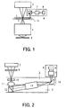
- FIG. 1 is a schematic sectional diagram of an exposure apparatus according to a first embodiment.
- 1 denotes an illumination optical system.
- a light from a laser is relayed by the illumination optical system 1, entering the reticle plane with a desirable light intensity distribution.
- a pellicle 3 is provided under a reticle 2 and prevents particles from adhering to a reticle plane.
- the reticle 2 is mounted on and driven by a reticle stage 2a.
- a light that has passed the reticle goes through a reduction projection optical system 4, and is imaged onto a wafer 5.
- a device (alignment scope) 6 observes a mark formed on the reticle plane.
- the reticle plane observing device 6 includes an optical system 7 and an image sensor 8.
- the optical system 7 has an objective lens, a relay lens, and a magnification-variable erector lens, and the image sensor 8 uses a two-dimensional charge-coupled device (CCD).
- the first embodiment measures an effective light source distribution using this configuration.
- a tool conjugate with the size of the reticle 2 and pellicle 3 is transported.
- the tool is located in a space from where the reticle 2 and the pellicle 3 are removed, thus needing no additional spaces.
- FIG. 2 is a partially enlarged transverse sectional view of the tool, and it can be understood that the optical system is stored in a housing conjugate with the reticle 2 and the pellicle 3 in size.
- the housing is mounted on and driven by the reticle stage.
- This embodiment includes a collimator lens 11 explained later configured to collimate the light and a deflector 12 configured to bent the light, and reduces a thickness of the housing within the size of the reticle 2 and the pellicle 3.
- the tool uses a driving mechanism for the reticle stage 2a and the alignment scope 6, and requires no dedicated driving mechanism.
- the light relayed from the light source by the illumination optical system 1 narrows down to a necessary area through a masking blade 9 that restricts the illumination area on the reticle plane, and enters a pinhole 10.
- the pinhole 10 may be slightly defocused from a plane conjugate with the reticle plane for spatial convenience.
- the collimator lens 11 substantially collimates the light that has passed through the pinhole 10.
- the deflector 12 such as a mirror or prism, the illumination light having been turned into collimated light enters a Fourier transforming optical system 13.
- An aerial pupil image is formed by the Fourier transforming optical system 13 at a position conjugate with the observation plane of the reticle plane observing element 6, and it is imaged at an approximately conjugate image sensor 8, thus measuring a light amount distribution through image processing. Based on this light amount and an observation diameter in the image sensor 8, a coordinate is calculated for a conversion into an effective light source distribution of an illumination optical system.
- the first embodiment observes an image using the image sensor 8, and the position of the pinhole 10 and the observation position of the image sensor 8 may be in an imaging relationship.
- Stopping down the illumination light by the masking blade 9 reduces the influence by the stray light (unnecessary light).
- An aperture of the masking blade 9 should not be so small as to shut out the light incident upon the pinhole 10, and it should be, desirably, set as small as possible.
- the pinhole 10 is formed on a Cr surface through etching. Desirably, the size and density of the Cr surface should be so large that stray light does not leak from illumination light stopped down by the masking blade 9.
- a mechanical light shield is provided with a sheet metal tiger-den material with holes around the pinhole 10.
- FIG. 3 briefly shows an optical system for the illumination light that is condensed by a condenser lens 16 from a fly-eye lens 15 to a pinhole 17 in a plane conjugate with the reticle plane in the illumination optical system.
- FIG. 3 shows a light that exits from the fly-eye lens 15 with a certain angle.
- the illumination light that passes the fly-eye lens 15 has a discrete angular distribution characteristic at one point on the reticle plane. This angular distribution characteristic depends upon the configuration of the fly-eye 15.
- L is an external diameter 18 of the fly-eye lens
- S is an outer diameter 20 of each fine lens comprising the fly-eye lens
- IllNA is an illumination system's NA conjugate with half of the outer diameter L
- the illumination light that has passed the pinhole 17 with a discrete angular distribution characteristic has a divergent angle due to diffraction, i.e., an airy disk 22.
- D can geometrically-optically separate each light when satisfying the following formula: D ⁇ 2 ⁇ H ⁇ S / L
- a pinhole diameter with a desired resolving power.
- An objective of setting a pinhole diameter is to separate light from a fly-eye lens for measurement, or to specify an amount of blurring at the beginning so as to set a pinhole diameter. In view of a dynamic range of the image sensor 8, light from the fly-eye lens may not be separated.
- the first embodiment sets the diameter of the pinhole 10 to ⁇ 50 ⁇ m. In order to control blurring caused by an aberration of a lens system, a tolerance for a lens system's distortion is relaxed, and the distortion is corrected by using image processing software.
- the above pinhole diameter determination method can be applied across all the pupil plane light intensity distribution measurements for an exposure apparatus using a pinhole.
- the illumination light on a reticle plane contemplates a maximum NA of 0.25 to 0.35 for an immersion exposure apparatus, although depending on an illumination condition.
- the first embodiment has prepared a collimator lens 11 that collimates the illumination light that has passed through the pinhole 10. Besides using a collimator lens, it is possible to use a deflector having a curvature.
- FIG. 4 is a plan view when the tool for measuring the effective light source distribution is viewed from the laser incident side.
- An area 24 is a size of a plane conjugate with the reticle plane.
- An optical system 25b shows a profile of the tool shown in FIG. 2, which measures the illumination system's on-axis effective light source distribution.
- Optical systems 25a and 25c measure the illumination system's off-axis effective light source distribution.
- the optical system 25 includes a pinhole 26 for the illumination light and a light exit position 27 that introduces the illumination light into the reticle plane observing device 6.
- the reticle stage supports the reticle and moves in a y direction or a scanning direction in FIG. 4:
- the reticle plane observing device 6 moves in an x direction. Since the pinhole 10 and the optical system 25 are housed within the tool, the two-dimensional movements guide the tool to a measuring position.
- a method of moving the tool to a measuring position may be a scanning search for a light source, or may use an alignment mark.
- the scanning search for the light source takes time before measuring.
- the alignment mark has a high reproducibility, and enables a light intensity distribution to be measured by a designated coordinate.
- the optical system 25 can move in the X direction, and provides an measurement of an illuminating system's effective light source distribution with a required image height. If each optical system 25 uses the same optical system, they are viable even if rotated by 180°. This configuration calibrates the optical system 7 of the reticle plane observing device 6 and the optical system 25 of the tool.
- the first embodiment almost maintains telecentric an aerial pupil image of the Fourier transforming optical system 13.
- the collimated light at the observation position of the reticle plane observing device 6 controls a size measurement error caused by a defocus.
- a known aperture stop and the like calculate an absolute value of a ⁇ distribution observable by the image sensor 8 and the central position of the image sensor 8, and correct an optical system's aberration such as a distortion.
- the reticle plane observing device 6 can defocus the observation position. Defocusing the observation position, measuring two or more pupil plane illumination distributions, and finding its centroid shift can measure the inclination of illumination light. This result represents an inclination of the illumination light on the reticle plane, and the so-called telecentricity is obtained by subtracting telecentricity of the projection optical system from it.
- a reference position of the image sensor is previously measured for each image height, an measurement at only the best focus position provides the inclination of the illumination light.
- the tool or reticle plane observing device 6 houses a beam splitter and analyzer, and they are switched, an effective light source distribution can be measured for each polarized light at the time of polarization illumination.
- the configuration of the present embodiment can provide a measurement of an illumination system's effective light source distribution corresponding to a scan o.
- the light intensity distribution at each position imaged on a wafer will become a scanning accumulation with the entire illumination slit.
- a scanning effective light source distribution is different from a stationary effective light source distribution. It is important to measure an actual effective light source distribution corresponding to the scan ⁇ .
- a scanning effective light source distribution can be measured with a slit that elongates in the scanning direction instead of a pinhole. An accumulation of obtained light intensity distributions in the scanning direction provides an actual scanning effective light source distribution. Use of a slit that is longer in the scanning direction than the illuminated area may provide a scanning effective light source distribution through only one measurement.
- the effective light source distribution of an illumination optical system measured in this embodiment can be utilized to adjust and correct the illumination optical system. Since measurement results are outputted from the reticle plane observing device 6, its calibration with the exposure apparatus body is easy.
- the projection optical system's transmittance can be obtained when an effective light source distribution on a wafer plane is compared with an effective light source distribution on a reticle plane of this embodiment.
- an effective light source distribution measuring tool which also includes an image sensor according to the present invention, to measure an effective light source distribution of an illumination system.
- the second embodiment is different from the first embodiment in that the tool also includes the image sensor, and measures an effective light source distribution without using the reticle plane observing device 6.
- This embodiment transports a tool that is as large as the reticle 2 and pellicle 3 in place of the ordinary reticle, and has a pinhole, an optical system, and an image sensor.
- FIG. 5 shows a transverse sectional view of the tool.
- a light relayed from a light source by an illumination optical system 1 narrows down to a necessary area through the masking blade 9 that limits the illumination area on a reticle plane, and enters the pinhole 10.
- the light that has passed through the pinhole 10 becomes almost collimated light via the collimator lens 11.
- the collimated illumination light is incident on the Fourier transforming optical system 13 through the deflector 12 such as a mirror and prism.
- a light source image is formed by the Fourier transforming optical system that is equivalent with a light intensity distribution on an exit pupil plane of the optical system, and an effective light source distribution is measured by the image sensor 28.
- This embodiment uses a wireless communication as a data communication means. Data acquired by the image sensor 28 is sent directly to the apparatus body using a wireless communication unit 29.
- a third embodiment of the present invention uses the effective light source distribution obtained in the first and second embodiments to adjust an illumination system and evaluate the imaging performance.
- step 1010 provides two wafer stages - one for exposure and one for measurement.
- the stage for measurement can be driven for measurements during exposure, and the throughput improves.
- the wafer stage for exposure is for immersion in this embodiment, but the stage for measurement is not provided for immersion. Therefore, even if a pinhole that is formed by etching glass with Cr is used, no problems occur about the concentration and durability of Cr against the immersion liquid.
- the transmittance distribution of the pupil in the projection optical system 4 is calculated from the results of steps 1006 and 1010 (Step 1012).
- an aberration of the projection optical system is measured in the exposure apparatus simultaneously (Step 1014).
- the imaging performance is calculated based on the effective light source distribution is calculated on the reticle plane or the wafer plane, the transmittance distribution of the projection optical system's pupil, the projection optical system's aberration, the projection optical system's NA, the reticle pattern to be used, and the wavelength to be used (Step 1016).
- This imaging performance is compared with a target imaging performance (Step 1018), and if out of the permissible range, at least one of the effective light source distribution, the projection optical system's aberration, and its NA are adjusted (Step 1020).
- the comparing items with the target imaging performance include the critical dimension ("CD") uniformity and the HV difference, OPE calculation, etc.
- the second and subsequent adjustments direct to the target values by calculating sensitivity.
- the adjustment ends (Step 1022).
- An automatic series of adjustments are preferable.
- the pupil's transmittance and aberration of the projection optical system need not be measured in the exposure apparatus body. However, they may be measured when the exposure apparatus is assembled, and the data may be used for calculation.
- This embodiment can quickly adjust the effective light source distribution of an illumination system and aberration of a projection optical system.
- This optimization which is not for each unit such as an illumination system or projection system, but for a whole exposure apparatus that is installed with an illumination system and projection system, is suitable for actual exposure of a wafer.
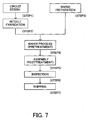
- FIG. 7 is a flowchart for explaining a fabrication of devices (semiconductor chips such as IC and LSI, LCDs, CCDs, etc.).
- a description will be given of a fabrication of a semiconductor chip as an example.
- Step 1 circuit design
- Step 2 reticle fabrication
- Step 3 wafer preparation
- Step 4 wafer process
- Step 5 assembly
- Step 6 inspection
- FIG. 8 is a detailed flowchart of the wafer process in Step 4.
- Step 11 oxidation
- Step 12 CVD
- Step 13 electrode formation
- Step 14 ion implantation
- Step 15 resist process
- Step 16 exposure
- Step 17 development
- Step 18 etching
- Step 19 resist stripping
- the above embodiments can measure an effective light source distribution without an additional space. These embodiments can be applied to existing exposure apparatuses having no means for accurately measuring effective light distributions. These embodiments calculate a blur of a light that passes a pinhole, and correct it in accordance with the geometrical optics and wave optics, thus providing a measurement of the original light source distribution. Since the illumination light is maintained almost telecentric at the observation position of the image sensor, the incidence sensitivity characteristic on the image sensor is small, and the measurement can be more accurate than ever.
- the illumination system's effective light source distribution acquired from these embodiments can be utilized as an index in adjusting a coherence factor ⁇ and telecentricity obtained from the effective light source distribution.
- Use of an acquired light intensity distribution for an imaging simulation enables the imaging performance to be evaluated.
- Actually measured data can be directly used as an illumination system's light intensity distribution in designing a diffraction optical element.
- a measuring apparatus used for an exposure apparatus that includes an illumination optical system that illuminates a reticle using light from a light source, a reticle stage that supports and drives the reticle, and a projection optical system that projects a pattern of the reticle onto a plate measures an effective light source distribution as an incident angular distribution of the light on a reticle plane of the reticle includes a relaying optical system configured to guide the light that has passed the illumination optical system, and a housing that contains the relaying optical system and is mounted on the reticle stage in place of the reticle.
Abstract
Description
- The present invention relates generally to a measuring apparatus, and more particularly to a measuring apparatus of an incident angular distribution or a light distribution characteristic (also called "an effective light source" and "a σ distribution") on an illuminated plane. Here, a measurement of an effective light source distribution of an illumination optical system intends to cover not only a measurement of the σ distribution but also a measurement of the centroid (or center of gravity) of illumination light.
- A projection exposure apparatus, which is conventionally used for the photolithography technique to manufacture fine semiconductor devices, projects a circuit pattern of a reticle (mask) onto a wafer and the like via a projection optical system, thus transferring the circuit pattern.
- Along with the recent demand on finer and lower profile electronic devices, finer semiconductor devices mounted on these electronic devices are increasingly demanded. A higher quality exposure requires an effective light source optimal to a reticle pattern. An effective light source distribution depends upon an adjustment of a light intensity distribution near an exit plane of, e.g., a fly-eye lens to a desired shape such as a normal illumination shape, an annular illumination shape, and a quadrupole illumination shape. Moreover, a projection exposure apparatus is demanded to control its numerical aperture ("NA"), coherence factor σ (which is an illumination optical system's NA / a projection optical system's NA), and an effective light source, thus setting up a condition optimal to each of various characteristics.
- Control over the coherence factor σ needs a more accurate measurement of an effective light source distribution. A measurement of a light intensity distribution on a lens' incident pupil plane will provides the effective light source distribution. The measurement of the effective light source distribution also provides a measurement of the centroid of illumination light on the incident pupil plane, which causes an asymmetry of the imaging performance, i.e., the so-called telecentricity.
- The conventional method of measuring the light intensity distribution on the pupil plane is seen, for example, in
Japanese Patent No. 2,928,277 Japanese Patent Applications, Publication Nos. 2000-19012 5-74687 2002-110540 - These conventional measurement methods require, in addition to a reticle, etc., a measuring apparatus such as a mirror, a condenser optical system, a relaying optical system, an image sensor and the like to be arranged on a plane or planes conjugate with reticle and wafer planes. However, an accommodation of these components in an exposure apparatus would increase the cost due to its limited capacity. In addition, such measurement methods should be applicable to an immersion exposure apparatus.
- The present invention is directed to a measuring apparatus, as well as an exposure apparatus having the same, that can measure a light source distribution without an additional space.
- A measuring apparatus according to one aspect of the present invention used for an exposure apparatus that includes an illumination optical system that illuminates a reticle using light from a light source, a reticle stage that supports and drives the reticle, and a projection optical system that projects a pattern of the reticle onto a plate measures an effective light source distribution as an incident angular distribution of the light on a reticle plane of the reticle includes a relaying optical system configured to guide the light that has passed the illumination optical system, and a housing that contains the relaying optical system and is mounted on the reticle stage in place of the reticle.
- A measuring apparatus according to another aspect of the present invention in an exposure apparatus that includes an illumination optical system that illuminates a reticle by using a light from a light source, and a projection optical system that projects a pattern of the reticle onto a plate measures an effective light source distribution as an incident angular distribution on a reticle plane of the light, and includes a pinhole member configured to transmit the light that has passed the illumination optical system into a pinhole with a diameter determined by a blur of a geometrical optics and wave optics, and a deflector configured to deflect the light that has passed through the pinhole.
- An exposure apparatus having the above measuring apparatus constitutes still another aspect of the present invention.
- An exposure method according to another aspect of the present invention includes the steps of calculating a pupil transmittance distribution in a projection optical system based on a first effective light source distribution of the projection optical system acquired by the above measuring apparatus, and a second effective light source distribution derived from a pupil plane light intensity distribution measured on a plate plane using a light that has passed the projection optical system without a reticle, calculating an imaging performance by using a result of the calculating step and the first or second effective light source distributions, adjusting the effective light source distribution and/or the projection optical system by using the imaging performance, and exposing the plate based on the effective light source distribution and/or the projection optical system that have been adjusted.
- A device manufacturing method including the steps of exposing a plate using the above exposure apparatus, and developing the plate exposed constitutes another aspect of the present invention.
- Other objects and further features of the present invention will become readily apparent from the following description of the preferred embodiments with reference to the accompanying drawings.
- FIG. 1 is a schematic sectional view of an exposure apparatus according to one aspect of the present invention.
- FIG. 2 is a transverse sectional view of a tool for measuring a light intensity distribution, applicable to a first embodiment of the present invention.
- FIG. 3 is a schematic view showing setting conditions for the diameter of a pinhole shown FIG. 2.
- FIG. 4 is a plan view of the tool shown in FIG. 2.
- FIG. 5 is a transverse sectional view of a tool for measuring a light intensity distribution, applicable to a second embodiment of the present invention.
- FIG. 6 is a flowchart for a σ adjustment and aberration correction method in a third embodiment of the present invention.
- FIG. 7 is a flowchart for explaining a fabrication of devices (such semiconductor chips as Ics, LSIs, and the like, LCDs, CCDs, etc.).
- FIG. 8 is a flowchart for a wafer process shown in FIG. 8.
- Referring to the accompanying drawings, a description will be now given of exposure apparatuses according to various embodiments of the present invention. These exposure apparatuses are step-and-scan projection exposure apparatuses, but they are also applicable to a step-and-repeat type and other types.
- FIG. 1 is a schematic sectional diagram of an exposure apparatus according to a first embodiment. In FIG. 1, 1 denotes an illumination optical system. A light from a laser is relayed by the illumination
optical system 1, entering the reticle plane with a desirable light intensity distribution. Apellicle 3 is provided under areticle 2 and prevents particles from adhering to a reticle plane. Thereticle 2 is mounted on and driven by areticle stage 2a. - A light that has passed the reticle goes through a reduction projection
optical system 4, and is imaged onto awafer 5. In order to adjust the positioning and focusing of thereticle 2, a device (alignment scope) 6 observes a mark formed on the reticle plane. The reticleplane observing device 6 includes anoptical system 7 and animage sensor 8. Theoptical system 7 has an objective lens, a relay lens, and a magnification-variable erector lens, and theimage sensor 8 uses a two-dimensional charge-coupled device (CCD). - The first embodiment measures an effective light source distribution using this configuration. In place of a usual reticle, a tool conjugate with the size of the
reticle 2 andpellicle 3 is transported. The tool is located in a space from where thereticle 2 and thepellicle 3 are removed, thus needing no additional spaces. FIG. 2 is a partially enlarged transverse sectional view of the tool, and it can be understood that the optical system is stored in a housing conjugate with thereticle 2 and thepellicle 3 in size. The housing is mounted on and driven by the reticle stage. - This embodiment includes a
collimator lens 11 explained later configured to collimate the light and adeflector 12 configured to bent the light, and reduces a thickness of the housing within the size of thereticle 2 and thepellicle 3. The tool uses a driving mechanism for thereticle stage 2a and thealignment scope 6, and requires no dedicated driving mechanism. - The light relayed from the light source by the illumination
optical system 1 narrows down to a necessary area through amasking blade 9 that restricts the illumination area on the reticle plane, and enters apinhole 10. Thepinhole 10 may be slightly defocused from a plane conjugate with the reticle plane for spatial convenience. Thecollimator lens 11 substantially collimates the light that has passed through thepinhole 10. By using thedeflector 12 such as a mirror or prism, the illumination light having been turned into collimated light enters a Fourier transformingoptical system 13. An aerial pupil image is formed by the Fourier transformingoptical system 13 at a position conjugate with the observation plane of the reticleplane observing element 6, and it is imaged at an approximatelyconjugate image sensor 8, thus measuring a light amount distribution through image processing. Based on this light amount and an observation diameter in theimage sensor 8, a coordinate is calculated for a conversion into an effective light source distribution of an illumination optical system. The first embodiment observes an image using theimage sensor 8, and the position of thepinhole 10 and the observation position of theimage sensor 8 may be in an imaging relationship. - Stopping down the illumination light by the
masking blade 9 reduces the influence by the stray light (unnecessary light). An aperture of themasking blade 9 should not be so small as to shut out the light incident upon thepinhole 10, and it should be, desirably, set as small as possible. Thepinhole 10 is formed on a Cr surface through etching. Desirably, the size and density of the Cr surface should be so large that stray light does not leak from illumination light stopped down by themasking blade 9. For control over the largely remaining Cr surface transmission, a mechanical light shield is provided with a sheet metal tiger-den material with holes around thepinhole 10. - It is desirable that the diameter of the
pinhole 10 be so large as to measure a light intensity distribution with sufficient resolving power. As a factor for determining the resolving power, a blur of the distribution and the image sensor's resolving power can be considered. Here, using FIG. 3, an explanation is given of a blur of a distribution. FIG. 3 briefly shows an optical system for the illumination light that is condensed by acondenser lens 16 from a fly-eye lens 15 to apinhole 17 in a plane conjugate with the reticle plane in the illumination optical system. FIG. 3 shows a light that exits from the fly-eye lens 15 with a certain angle. The illumination light that passes the fly-eye lens 15 has a discrete angular distribution characteristic at one point on the reticle plane. This angular distribution characteristic depends upon the configuration of the fly-eye 15. The following equation is met where L is anexternal diameter 18 of the fly-eye lens 15, S is anouter diameter 20 of each fine lens comprising the fly-eye lens 15, IllNA is an illumination system's NA conjugate with half of the outer diameter L, and P is an NA's interval 21 of illumination light at the reticle plane:
- The illumination light that has passed the
pinhole 17 with a discrete angular distribution characteristic has a divergent angle due to diffraction, i.e., anairy disk 22. The following equation is met with a wavelength A and a pinhole's diameter ϕ, where A is adivergence angle 23 that corresponds to a first zero-point radius of this airy disk 22:
- Since respective light that has passed through the fly-
eye lens 15 are each affected by the diffraction, use of a pinhole diameter satisfying the following formula enables a light from each fly-eye lens to be wave-optically separated and measured:
- When using a lens system for measuring an effective light source distribution, a blur due to an aberration needs to be considered. Assume that the
image sensor 8's observation range radius corresponding to the illumination system'sNA 19 is H, and an RMS spot diameter due to an aberration is D. D can geometrically-optically separate each light when satisfying the following formula:
- Besides these items, it is desirable to consider the dose incident on the image sensor, and the image sensor's resolving power.
- These formulas define a pinhole diameter with a desired resolving power. An objective of setting a pinhole diameter is to separate light from a fly-eye lens for measurement, or to specify an amount of blurring at the beginning so as to set a pinhole diameter. In view of a dynamic range of the
image sensor 8, light from the fly-eye lens may not be separated. The first embodiment sets the diameter of thepinhole 10 to ϕ50µm. In order to control blurring caused by an aberration of a lens system, a tolerance for a lens system's distortion is relaxed, and the distortion is corrected by using image processing software. - The above pinhole diameter determination method can be applied across all the pupil plane light intensity distribution measurements for an exposure apparatus using a pinhole.
- The illumination light on a reticle plane contemplates a maximum NA of 0.25 to 0.35 for an immersion exposure apparatus, although depending on an illumination condition. In order to keep the tool within the size of the reticle and pellicle, it is necessary to control a spread of the effective diameter of the illumination light that has passed the
pinhole 10. For this purpose, the first embodiment has prepared acollimator lens 11 that collimates the illumination light that has passed through thepinhole 10. Besides using a collimator lens, it is possible to use a deflector having a curvature. - FIG. 4 is a plan view when the tool for measuring the effective light source distribution is viewed from the laser incident side. Although this embodiment uses two reticle plane observation systems, only one may be used. An
area 24 is a size of a plane conjugate with the reticle plane. An optical system 25b shows a profile of the tool shown in FIG. 2, which measures the illumination system's on-axis effective light source distribution.Optical systems 25a and 25c measure the illumination system's off-axis effective light source distribution. The optical system 25 includes a pinhole 26 for the illumination light and a light exit position 27 that introduces the illumination light into the reticleplane observing device 6. - In this embodiment, the reticle stage supports the reticle and moves in a y direction or a scanning direction in FIG. 4: The reticle
plane observing device 6 moves in an x direction. Since thepinhole 10 and the optical system 25 are housed within the tool, the two-dimensional movements guide the tool to a measuring position. - A method of moving the tool to a measuring position may be a scanning search for a light source, or may use an alignment mark. The scanning search for the light source takes time before measuring. On the other hand, the alignment mark has a high reproducibility, and enables a light intensity distribution to be measured by a designated coordinate.
- The optical system 25 can move in the X direction, and provides an measurement of an illuminating system's effective light source distribution with a required image height. If each optical system 25 uses the same optical system, they are viable even if rotated by 180°. This configuration calibrates the
optical system 7 of the reticleplane observing device 6 and the optical system 25 of the tool. - The first embodiment almost maintains telecentric an aerial pupil image of the Fourier transforming
optical system 13. The collimated light at the observation position of the reticleplane observing device 6 controls a size measurement error caused by a defocus. A known aperture stop and the like calculate an absolute value of a σ distribution observable by theimage sensor 8 and the central position of theimage sensor 8, and correct an optical system's aberration such as a distortion. - The reticle
plane observing device 6 can defocus the observation position. Defocusing the observation position, measuring two or more pupil plane illumination distributions, and finding its centroid shift can measure the inclination of illumination light. This result represents an inclination of the illumination light on the reticle plane, and the so-called telecentricity is obtained by subtracting telecentricity of the projection optical system from it. Of course, when a reference position of the image sensor is previously measured for each image height, an measurement at only the best focus position provides the inclination of the illumination light. - When the tool or reticle
plane observing device 6 houses a beam splitter and analyzer, and they are switched, an effective light source distribution can be measured for each polarized light at the time of polarization illumination. - The configuration of the present embodiment can provide a measurement of an illumination system's effective light source distribution corresponding to a scan o. In a step-and-scan exposure apparatus, the light intensity distribution at each position imaged on a wafer will become a scanning accumulation with the entire illumination slit. A scanning effective light source distribution is different from a stationary effective light source distribution. It is important to measure an actual effective light source distribution corresponding to the scan σ.
- A scanning effective light source distribution can be measured with a slit that elongates in the scanning direction instead of a pinhole. An accumulation of obtained light intensity distributions in the scanning direction provides an actual scanning effective light source distribution. Use of a slit that is longer in the scanning direction than the illuminated area may provide a scanning effective light source distribution through only one measurement.
- The effective light source distribution of an illumination optical system measured in this embodiment can be utilized to adjust and correct the illumination optical system. Since measurement results are outputted from the reticle
plane observing device 6, its calibration with the exposure apparatus body is easy. The projection optical system's transmittance can be obtained when an effective light source distribution on a wafer plane is compared with an effective light source distribution on a reticle plane of this embodiment. - Next follows a second embodiment that uses an effective light source distribution measuring tool, which also includes an image sensor according to the present invention, to measure an effective light source distribution of an illumination system. The second embodiment is different from the first embodiment in that the tool also includes the image sensor, and measures an effective light source distribution without using the reticle
plane observing device 6. - This embodiment transports a tool that is as large as the
reticle 2 andpellicle 3 in place of the ordinary reticle, and has a pinhole, an optical system, and an image sensor. FIG. 5 shows a transverse sectional view of the tool. A light relayed from a light source by an illuminationoptical system 1 narrows down to a necessary area through themasking blade 9 that limits the illumination area on a reticle plane, and enters thepinhole 10. The light that has passed through thepinhole 10 becomes almost collimated light via thecollimator lens 11. The collimated illumination light is incident on the Fourier transformingoptical system 13 through thedeflector 12 such as a mirror and prism. A light source image is formed by the Fourier transforming optical system that is equivalent with a light intensity distribution on an exit pupil plane of the optical system, and an effective light source distribution is measured by theimage sensor 28. - This embodiment uses a wireless communication as a data communication means. Data acquired by the
image sensor 28 is sent directly to the apparatus body using awireless communication unit 29. - A third embodiment of the present invention uses the effective light source distribution obtained in the first and second embodiments to adjust an illumination system and evaluate the imaging performance. FIG. 6 shows a flowchart of this method. Initially, an illumination condition for optimization is determined. In order to define the size of σ = 1, an illumination optical system's condition is set for σ = 1 (Step 1002). Next follows a transportation of the above tool (Step 1004). Then, an effective light source distribution is set for the illumination system (Step 1006). Then, the tool is taken out (Step 1008).
- Next, the light intensity distribution on the pupil plane is measured while the
reticle 2 and thepellicle 3 are removed (Step 1010). For an immersion exposure apparatus,step 1010 provides two wafer stages - one for exposure and one for measurement. Thus, the stage for measurement can be driven for measurements during exposure, and the throughput improves. In addition, the wafer stage for exposure is for immersion in this embodiment, but the stage for measurement is not provided for immersion. Therefore, even if a pinhole that is formed by etching glass with Cr is used, no problems occur about the concentration and durability of Cr against the immersion liquid. - The transmittance distribution of the pupil in the projection
optical system 4 is calculated from the results ofsteps 1006 and 1010 (Step 1012). In addition, an aberration of the projection optical system is measured in the exposure apparatus simultaneously (Step 1014). - The imaging performance is calculated based on the effective light source distribution is calculated on the reticle plane or the wafer plane, the transmittance distribution of the projection optical system's pupil, the projection optical system's aberration, the projection optical system's NA, the reticle pattern to be used, and the wavelength to be used (Step 1016). This imaging performance is compared with a target imaging performance (Step 1018), and if out of the permissible range, at least one of the effective light source distribution, the projection optical system's aberration, and its NA are adjusted (Step 1020). The comparing items with the target imaging performance include the critical dimension ("CD") uniformity and the HV difference, OPE calculation, etc. The second and subsequent adjustments direct to the target values by calculating sensitivity. When the current imaging performance is permissible range from the target imaging performance, the adjustment ends (Step 1022). An automatic series of adjustments are preferable. The pupil's transmittance and aberration of the projection optical system need not be measured in the exposure apparatus body. However, they may be measured when the exposure apparatus is assembled, and the data may be used for calculation.
- This embodiment can quickly adjust the effective light source distribution of an illumination system and aberration of a projection optical system. This optimization, which is not for each unit such as an illumination system or projection system, but for a whole exposure apparatus that is installed with an illumination system and projection system, is suitable for actual exposure of a wafer.
- Next, referring to FIGs. 7 and 8, a description will be given of an embodiment of a device manufacturing method using the exposure apparatus described above. FIG. 7 is a flowchart for explaining a fabrication of devices (semiconductor chips such as IC and LSI, LCDs, CCDs, etc.). Here, a description will be given of a fabrication of a semiconductor chip as an example. Step 1 (circuit design) designs a device circuit. Step 2 (reticle fabrication) forms a reticle having a designed circuit pattern. Step 3 (wafer preparation) manufactures a wafer using materials such as silicon. Step 4 (wafer process), which is referred to as a pretreatment, forms actual circuitry on the wafer through a lithography technique using the reticle and wafer. Step 5 (assembly), which is also referred to as a post-treatment, forms into a semiconductor chip the wafer formed in
Step 4 and includes an assembly step (e.g., dicing, bonding), a packaging step (chip sealing), and the like. Step 6 (inspection) performs various tests for the semiconductor device made inStep 5, such as a validity test and a durability test. Through these steps, a semiconductor device is finished and shipped (Step 7). - FIG. 8 is a detailed flowchart of the wafer process in
Step 4. Step 11 (oxidation) oxidizes the wafer's surface. Step 12 (CVD) forms an insulating film on the wafer's surface. Step 13 (electrode formation) forms electrodes on the wafer by vapor disposition and the like. Step 14 (ion implantation) implants ion into the wafer. Step 15 (resist process) applies a photosensitive material onto the wafer. Step 16 (exposure) uses the exposure apparatus to expose a circuit pattern of the reticle onto the wafer. Step 17 (development) develops the exposed wafer. Step 18 (etching) etches parts other than a developed resist image. Step 19 (resist stripping) removes disused resist after etching. These steps are repeated, and multilayer circuit patterns are formed on the wafer. Use of such a device manufacturing method enables higher quality devices to be manufactured than the prior art. In this manner, the device manufacturing method that uses the exposure apparatus, and the devices as a final product serve as other aspects according to the present invention. - The above embodiments can measure an effective light source distribution without an additional space. These embodiments can be applied to existing exposure apparatuses having no means for accurately measuring effective light distributions. These embodiments calculate a blur of a light that passes a pinhole, and correct it in accordance with the geometrical optics and wave optics, thus providing a measurement of the original light source distribution. Since the illumination light is maintained almost telecentric at the observation position of the image sensor, the incidence sensitivity characteristic on the image sensor is small, and the measurement can be more accurate than ever.
- The illumination system's effective light source distribution acquired from these embodiments can be utilized as an index in adjusting a coherence factor σ and telecentricity obtained from the effective light source distribution. Use of an acquired light intensity distribution for an imaging simulation enables the imaging performance to be evaluated. Actually measured data can be directly used as an illumination system's light intensity distribution in designing a diffraction optical element.
- Further, the present invention is not limited to these preferred embodiments, and various variations and modifications may be made without departing from the scope of the present invention.
- A measuring apparatus used for an exposure apparatus that includes an illumination optical system that illuminates a reticle using light from a light source, a reticle stage that supports and drives the reticle, and a projection optical system that projects a pattern of the reticle onto a plate measures an effective light source distribution as an incident angular distribution of the light on a reticle plane of the reticle includes a relaying optical system configured to guide the light that has passed the illumination optical system, and a housing that contains the relaying optical system and is mounted on the reticle stage in place of the reticle.
Claims (19)
- A measuring apparatus used for an exposure apparatus that includes an illumination optical system that illuminates a reticle using light from a light source, a reticle stage that supports and drives the reticle, and a projection optical system that projects a pattern of the reticle onto a plate, said measuring apparatus measuring an effective light source distribution as an incident angular distribution of the light on a reticle plane of the reticle, characterized in that said measuring apparatus comprises:a relaying optical system configured to guide the light that has passed the illumination optical system, and a housing that contains the relaying optical system and is mounted on the reticle stage in place of the reticle.
- A measuring apparatus according to claim 1, characterized in that the exposure apparatus further includes an alignment scope configured to observe an alignment mark used to align the reticle and the plate, and the relaying optical system guides the light that has passed the illumination optical system to the alignment scope.
- A measuring apparatus according to claim 1, characterized in that the relaying optical system includes a Fourier transforming optical system configured to generate an aerial pupil image from the light that has passed through a pinhole.
- A measuring apparatus according to claim 3, characterized in that a light exit end of the Fourier transforming optical system is conjugate with an image sensor of the alignment optical system.
- A measuring apparatus according to claim 3, characterized in that the pinhole is conjugate with an image sensor of the alignment optical system.
- A measuring apparatus according to claim 2, characterized in that said housing moves to a measuring position when the reticle stage moves in a scanning direction and the alignment optical system moves in a direction perpendicular to the scanning.
- A measuring apparatus according to claim 3, characterized in that said measuring apparatus further comprises a lens configured to collimate the light that has passed the pinhole.
- A measuring apparatus according to claim 1, characterized in that said housing includes an alignment mark for an alignment between the reticle and the plate.
- A measuring apparatus according to claim 1, characterized in that said housing can be transported by a transport system that transports the reticle.
- A measuring apparatus according to claim 1, characterized in that the reticle stage drives the relaying optical system and makes a measurement image height variable.
- A measuring apparatus according to claim 1, characterized in that said measuring apparatus further comprises a beam splitter configured to split the light, and an analyzer configured to generate a plane polarized light.
- A measuring apparatus according to claim 2, characterized in that the alignment optical system includes a beam splitter configured to split the light, and an analyzer configured to generate a plane polarized light.
- A measuring apparatus according to claim 3, characterized in that the pinhole has a slit shape that elongates in a scanning direction.
- A measuring apparatus according to claim 1, characterized in that the measuring apparatus further comprises an image sensor that senses an image of the effective light source distribution, and the relaying optical system guides the light that has passed the illumination optical system to said image sensor.
- A measuring apparatus in an exposure apparatus that includes an illumination optical system that illuminates a reticle by using a light from a light source, and a projection optical system that projects a pattern of the reticle onto a plate, said measuring apparatus measuring an effective light source distribution as an incident angular distribution on a reticle plane of the light, characterized in that said measuring apparatus comprises a pinhole member configured to transmit the light that has passed the illumination optical system into a pinhole with a diameter determined by a blur of a geometrical optics and wave optics, and a deflector configured to deflect the light that has passed through the pinhole.
- An exposure apparatus characterized in comprising the measuring apparatus according to any one of claims 1 to 15.
- An exposure method for adjusting an effective light source distribution and/or a projection optical system by using a imaging performance, and for exposing a plate based on the effective light source distribution and/or the projection optical system that have been adjusted, characterized in that said exposure method comprises the steps of:calculating a pupil transmittance distribution in the projection optical system based on a first effective light source distribution of the projection optical system acquired by a measuring apparatus according to any one of claims 1 to 15, and a second effective light source distribution derived from a pupil plane light intensity distribution measured on a plate plane using a light that has passed the projection optical system without a reticle, and calculating an imaging performance by using a result of said distribution calculating step and the first or second effective light source distributions;
- An exposure method according to claim 17, characterized in that said exposure method further comprises the steps of:determining whether an illumination condition, with which the illumination optical system illuminates the reticle, has been set or changed, and executing said pupil transmittance distribution calculating step, said imaging performance calculating step, and said adjusting step, when said determining step determines that the illumination condition has been set or changed.
- A device manufacturing method comprising the steps exposing a plate, and developing the plate exposed, characterized in that said exposing step uses an exposure apparatus according to claim 16.
Applications Claiming Priority (1)
| Application Number | Priority Date | Filing Date | Title |
|---|---|---|---|
| JP2005123006A JP2006303196A (en) | 2005-04-20 | 2005-04-20 | Measuring device and aligner having the same |
Publications (2)
| Publication Number | Publication Date |
|---|---|
| EP1715385A2 true EP1715385A2 (en) | 2006-10-25 |
| EP1715385A3 EP1715385A3 (en) | 2008-04-09 |
Family
ID=36754275
Family Applications (1)
| Application Number | Title | Priority Date | Filing Date |
|---|---|---|---|
| EP06112610A Withdrawn EP1715385A3 (en) | 2005-04-20 | 2006-04-13 | Measuring apparatus and exposure apparatus having the same |
Country Status (5)
| Country | Link |
|---|---|
| US (1) | US7671967B2 (en) |
| EP (1) | EP1715385A3 (en) |
| JP (1) | JP2006303196A (en) |
| KR (1) | KR100819240B1 (en) |
| TW (1) | TWI301635B (en) |
Cited By (1)
| Publication number | Priority date | Publication date | Assignee | Title |
|---|---|---|---|---|
| TWI594085B (en) * | 2014-11-21 | 2017-08-01 | 佳能股份有限公司 | Illumination optical apparatus and device manufacturing method |
Families Citing this family (7)
| Publication number | Priority date | Publication date | Assignee | Title |
|---|---|---|---|---|
| JP2006303196A (en) | 2005-04-20 | 2006-11-02 | Canon Inc | Measuring device and aligner having the same |
| JP2006332363A (en) * | 2005-05-26 | 2006-12-07 | Nikon Corp | Exposure device and illumination light intensity distribution measuring device thereof |
| JP2008108851A (en) * | 2006-10-24 | 2008-05-08 | Canon Inc | Illuminating means, exposure apparatus having the illuminating means, and manufacturing method of device |
| US20090002656A1 (en) | 2007-06-29 | 2009-01-01 | Asml Netherlands B.V. | Device and method for transmission image detection, lithographic apparatus and mask for use in a lithographic apparatus |
| JP5063229B2 (en) * | 2007-07-12 | 2012-10-31 | キヤノン株式会社 | Exposure apparatus and device manufacturing method |
| JP2009025553A (en) | 2007-07-19 | 2009-02-05 | Canon Inc | Phase shift mask |
| WO2019166183A1 (en) * | 2018-02-28 | 2019-09-06 | Asml Netherlands B.V. | Apodization measurement for lithographic apparatus |
Citations (2)
| Publication number | Priority date | Publication date | Assignee | Title |
|---|---|---|---|---|
| US20020085190A1 (en) * | 2000-12-28 | 2002-07-04 | Nikon Corporation | Manufacturing method in manufacturing line, manufacturing method for exposure apparatus, and exposure apparatus |
| US20040119973A1 (en) | 2002-08-30 | 2004-06-24 | Kazuya Fukuhara | Exposure apparatus inspection method and exposure apparatus |
Family Cites Families (24)
| Publication number | Priority date | Publication date | Assignee | Title |
|---|---|---|---|---|
| US5140366A (en) | 1987-05-29 | 1992-08-18 | Canon Kabushiki Kaisha | Exposure apparatus with a function for controlling alignment by use of latent images |
| US5475491A (en) | 1989-02-10 | 1995-12-12 | Canon Kabushiki Kaisha | Exposure apparatus |
| US5121160A (en) | 1989-03-09 | 1992-06-09 | Canon Kabushiki Kaisha | Exposure method and apparatus |
| JP2928277B2 (en) | 1989-08-03 | 1999-08-03 | 株式会社日立製作所 | Projection exposure method and apparatus |
| JPH0574687A (en) | 1991-09-18 | 1993-03-26 | Hitachi Ltd | Projection exposing device |
| JP3278896B2 (en) | 1992-03-31 | 2002-04-30 | キヤノン株式会社 | Illumination apparatus and projection exposure apparatus using the same |
| JP2946950B2 (en) | 1992-06-25 | 1999-09-13 | キヤノン株式会社 | Illumination apparatus and exposure apparatus using the same |
| JP2698521B2 (en) * | 1992-12-14 | 1998-01-19 | キヤノン株式会社 | Catadioptric optical system and projection exposure apparatus having the optical system |
| US6757050B1 (en) | 1992-12-28 | 2004-06-29 | Canon Kabushiki Kaisha | Exposure method and apparatus for detecting an exposure amount and for calculating a correction value based on the detected exposure amount |
| JP2862477B2 (en) | 1993-06-29 | 1999-03-03 | キヤノン株式会社 | Exposure apparatus and method for manufacturing device using the exposure apparatus |
| JP3057998B2 (en) | 1994-02-16 | 2000-07-04 | キヤノン株式会社 | Illumination device and projection exposure apparatus using the same |
| JP3060357B2 (en) | 1994-06-22 | 2000-07-10 | キヤノン株式会社 | Scanning exposure apparatus and device manufacturing method using the scanning exposure apparatus |
| JP3412981B2 (en) * | 1995-08-29 | 2003-06-03 | キヤノン株式会社 | Projection exposure apparatus and projection exposure method |
| KR100210569B1 (en) | 1995-09-29 | 1999-07-15 | 미따라이 하지메 | Exposure method and exposure apparatus and method for manufacturing device using the same |
| KR970028865A (en) * | 1995-11-16 | 1997-06-24 | 오노 시게오 | Exposure apparatus and exposure method |
| JPH09180989A (en) * | 1995-12-26 | 1997-07-11 | Toshiba Corp | Exposure system and method |
| JP2691341B2 (en) * | 1996-05-27 | 1997-12-17 | 株式会社ニコン | Projection exposure equipment |
| KR100525067B1 (en) * | 1997-01-20 | 2005-12-21 | 가부시키가이샤 니콘 | Method for measuring optical feature of exposure apparatus and exposure apparatus having means for measuring optical feature |
| JP2000019012A (en) | 1998-07-03 | 2000-01-21 | Nikon Corp | Lighting system brightness distribution measuring device |
| JP3927753B2 (en) | 2000-03-31 | 2007-06-13 | キヤノン株式会社 | Exposure apparatus and device manufacturing method |
| US6710856B2 (en) * | 2000-09-01 | 2004-03-23 | Asml Netherlands B.V. | Method of operating a lithographic apparatus, lithographic apparatus, method of manufacturing a device, and device manufactured thereby |
| JP4343685B2 (en) * | 2001-08-31 | 2009-10-14 | キヤノン株式会社 | Reticle and optical property measurement method |
| JP5143331B2 (en) | 2003-05-28 | 2013-02-13 | 株式会社ニコン | Exposure method, exposure apparatus, and device manufacturing method |
| JP2006303196A (en) | 2005-04-20 | 2006-11-02 | Canon Inc | Measuring device and aligner having the same |
-
2005
- 2005-04-20 JP JP2005123006A patent/JP2006303196A/en not_active Abandoned
-
2006
- 2006-04-13 EP EP06112610A patent/EP1715385A3/en not_active Withdrawn
- 2006-04-14 TW TW095113447A patent/TWI301635B/en not_active IP Right Cessation
- 2006-04-18 US US11/405,472 patent/US7671967B2/en not_active Expired - Fee Related
- 2006-04-20 KR KR1020060035535A patent/KR100819240B1/en not_active IP Right Cessation
Patent Citations (2)
| Publication number | Priority date | Publication date | Assignee | Title |
|---|---|---|---|---|
| US20020085190A1 (en) * | 2000-12-28 | 2002-07-04 | Nikon Corporation | Manufacturing method in manufacturing line, manufacturing method for exposure apparatus, and exposure apparatus |
| US20040119973A1 (en) | 2002-08-30 | 2004-06-24 | Kazuya Fukuhara | Exposure apparatus inspection method and exposure apparatus |
Cited By (2)
| Publication number | Priority date | Publication date | Assignee | Title |
|---|---|---|---|---|
| TWI594085B (en) * | 2014-11-21 | 2017-08-01 | 佳能股份有限公司 | Illumination optical apparatus and device manufacturing method |
| US10133185B2 (en) | 2014-11-21 | 2018-11-20 | Canon Kabushiki Kaisha | Illumination optical apparatus and device manufacturing method |
Also Published As
| Publication number | Publication date |
|---|---|
| KR20060110809A (en) | 2006-10-25 |
| EP1715385A3 (en) | 2008-04-09 |
| TWI301635B (en) | 2008-10-01 |
| KR100819240B1 (en) | 2008-04-02 |
| JP2006303196A (en) | 2006-11-02 |
| US7671967B2 (en) | 2010-03-02 |
| US20060238736A1 (en) | 2006-10-26 |
| TW200705547A (en) | 2007-02-01 |
Similar Documents
| Publication | Publication Date | Title |
|---|---|---|
| US7423740B2 (en) | Reticle and optical characteristic measuring method | |
| US7619748B2 (en) | Exposure apparatus mounted with measuring apparatus | |
| US7088426B2 (en) | Projection optical system adjustment method, prediction method, evaluation method, adjustment method, exposure method and exposure apparatus, program, and device manufacturing method | |
| JP4343706B2 (en) | Reticle and optical property measurement method | |
| US6960415B2 (en) | Aberration measuring method and projection exposure apparatus | |
| US7671967B2 (en) | Exposure apparatus and exposure method | |
| US7304749B2 (en) | Point diffraction interferometer and exposure apparatus and method using the same | |
| JP2002198303A (en) | Aligner, optical characteristic measuring method and method for manufacturing device | |
| KR100756139B1 (en) | Exposure apparatus and device manufacturing method using the same | |
| US7295326B2 (en) | Apparatus and method for measuring the optical performance of an optical element | |
| US7826044B2 (en) | Measurement method and apparatus, and exposure apparatus | |
| JP3994209B2 (en) | Optical system inspection apparatus and inspection method, and alignment apparatus and projection exposure apparatus provided with the inspection apparatus | |
| JP5503193B2 (en) | Wavefront aberration measuring apparatus, exposure apparatus, and device manufacturing method | |
| JP2008186912A (en) | Method for evaluating aberration, adjusting method, exposure device, exposure method and manufacturing method for device | |
| JP4143614B2 (en) | Measuring method | |
| KR20080088480A (en) | Aberration measurement method, exposure apparatus, and device manufacturing method | |
| JP2002195913A (en) | Apparatus and method for measuring aberration, exposure apparatus and method for producing device | |
| JP3673783B2 (en) | Aberration measuring method and projection exposure apparatus | |
| JPH0949781A (en) | Inspecting device for optical system and projection exposure apparatus with the inspecting device | |
| JP2008172004A (en) | Aberration evaluating method, adjusting method, exposure device, exposure method and device manufacturing method | |
| JPH10284414A (en) | Imaging position detecting apparatus and manufacture of semiconductor device | |
| JP2006053056A (en) | Position measuring method, position measuring instrument, aligner, and device manufacturing method | |
| JP2004128149A (en) | Aberration measuring method, exposure method and aligner | |
| US20230050291A1 (en) | Method and device for correcting a telecentricity error of an imaging device | |
| JP2000214047A (en) | Inspecting device for optical system, alignment device equipped with this inspecting device, and projection aligner |
Legal Events
| Date | Code | Title | Description |
|---|---|---|---|
| PUAI | Public reference made under article 153(3) epc to a published international application that has entered the european phase |
Free format text: ORIGINAL CODE: 0009012 |
|
| AK | Designated contracting states |
Kind code of ref document: A2 Designated state(s): AT BE BG CH CY CZ DE DK EE ES FI FR GB GR HU IE IS IT LI LT LU LV MC NL PL PT RO SE SI SK TR |
|
| AX | Request for extension of the european patent |
Extension state: AL BA HR MK YU |
|
| PUAL | Search report despatched |
Free format text: ORIGINAL CODE: 0009013 |
|
| AK | Designated contracting states |
Kind code of ref document: A3 Designated state(s): AT BE BG CH CY CZ DE DK EE ES FI FR GB GR HU IE IS IT LI LT LU LV MC NL PL PT RO SE SI SK TR |
|
| AX | Request for extension of the european patent |
Extension state: AL BA HR MK YU |
|
| 17P | Request for examination filed |
Effective date: 20081009 |
|
| AKX | Designation fees paid |
Designated state(s): DE IT NL |
|
| 17Q | First examination report despatched |
Effective date: 20100917 |
|
| STAA | Information on the status of an ep patent application or granted ep patent |
Free format text: STATUS: THE APPLICATION HAS BEEN WITHDRAWN |
|
| 18W | Application withdrawn |
Effective date: 20101025 |