EP1717912B1 - Low cross talk and impedance controlled electrical connector - Google Patents
Low cross talk and impedance controlled electrical connector Download PDFInfo
- Publication number
- EP1717912B1 EP1717912B1 EP06007681.7A EP06007681A EP1717912B1 EP 1717912 B1 EP1717912 B1 EP 1717912B1 EP 06007681 A EP06007681 A EP 06007681A EP 1717912 B1 EP1717912 B1 EP 1717912B1
- Authority
- EP
- European Patent Office
- Prior art keywords
- dielectric
- receptacle
- plug
- ground
- metallic pins
- Prior art date
- Legal status (The legal status is an assumption and is not a legal conclusion. Google has not performed a legal analysis and makes no representation as to the accuracy of the status listed.)
- Expired - Lifetime
Links
Images


Classifications
-
- H—ELECTRICITY
- H01—ELECTRIC ELEMENTS
- H01R—ELECTRICALLY-CONDUCTIVE CONNECTIONS; STRUCTURAL ASSOCIATIONS OF A PLURALITY OF MUTUALLY-INSULATED ELECTRICAL CONNECTING ELEMENTS; COUPLING DEVICES; CURRENT COLLECTORS
- H01R13/00—Details of coupling devices of the kinds covered by groups H01R12/70 or H01R24/00 - H01R33/00
- H01R13/648—Protective earth or shield arrangements on coupling devices, e.g. anti-static shielding
- H01R13/652—Protective earth or shield arrangements on coupling devices, e.g. anti-static shielding with earth pin, blade or socket
-
- H—ELECTRICITY
- H01—ELECTRIC ELEMENTS
- H01P—WAVEGUIDES; RESONATORS, LINES, OR OTHER DEVICES OF THE WAVEGUIDE TYPE
- H01P3/00—Waveguides; Transmission lines of the waveguide type
- H01P3/02—Waveguides; Transmission lines of the waveguide type with two longitudinal conductors
- H01P3/08—Microstrips; Strip lines
- H01P3/085—Triplate lines
-
- H—ELECTRICITY
- H01—ELECTRIC ELEMENTS
- H01R—ELECTRICALLY-CONDUCTIVE CONNECTIONS; STRUCTURAL ASSOCIATIONS OF A PLURALITY OF MUTUALLY-INSULATED ELECTRICAL CONNECTING ELEMENTS; COUPLING DEVICES; CURRENT COLLECTORS
- H01R12/00—Structural associations of a plurality of mutually-insulated electrical connecting elements, specially adapted for printed circuits, e.g. printed circuit boards [PCB], flat or ribbon cables, or like generally planar structures, e.g. terminal strips, terminal blocks; Coupling devices specially adapted for printed circuits, flat or ribbon cables, or like generally planar structures; Terminals specially adapted for contact with, or insertion into, printed circuits, flat or ribbon cables, or like generally planar structures
- H01R12/70—Coupling devices
- H01R12/71—Coupling devices for rigid printing circuits or like structures
- H01R12/712—Coupling devices for rigid printing circuits or like structures co-operating with the surface of the printed circuit or with a coupling device exclusively provided on the surface of the printed circuit
- H01R12/716—Coupling device provided on the PCB
-
- H—ELECTRICITY
- H01—ELECTRIC ELEMENTS
- H01R—ELECTRICALLY-CONDUCTIVE CONNECTIONS; STRUCTURAL ASSOCIATIONS OF A PLURALITY OF MUTUALLY-INSULATED ELECTRICAL CONNECTING ELEMENTS; COUPLING DEVICES; CURRENT COLLECTORS
- H01R13/00—Details of coupling devices of the kinds covered by groups H01R12/70 or H01R24/00 - H01R33/00
- H01R13/646—Details of coupling devices of the kinds covered by groups H01R12/70 or H01R24/00 - H01R33/00 specially adapted for high-frequency, e.g. structures providing an impedance match or phase match
- H01R13/6461—Means for preventing cross-talk
- H01R13/6471—Means for preventing cross-talk by special arrangement of ground and signal conductors, e.g. GSGS [Ground-Signal-Ground-Signal]
-
- H—ELECTRICITY
- H01—ELECTRIC ELEMENTS
- H01R—ELECTRICALLY-CONDUCTIVE CONNECTIONS; STRUCTURAL ASSOCIATIONS OF A PLURALITY OF MUTUALLY-INSULATED ELECTRICAL CONNECTING ELEMENTS; COUPLING DEVICES; CURRENT COLLECTORS
- H01R43/00—Apparatus or processes specially adapted for manufacturing, assembling, maintaining, or repairing of line connectors or current collectors or for joining electric conductors
- H01R43/02—Apparatus or processes specially adapted for manufacturing, assembling, maintaining, or repairing of line connectors or current collectors or for joining electric conductors for soldered or welded connections
Definitions
- Document US 4,605,278 relates to solder-bearing lead useful as a terminal or contact, which may be fabricated by rapid progressive stamping techniques, for use with multiple contact connectors and electronic circuit boards.
- Document 4,679,889 is a continuation of the above mentioned US 4,605,278 and relates to the same technology.
- Document JP 6243936 relates to an impedance matching type electric connector according to the preamble of claim 1, for connecting for example printed circuit boards with each other.
- a plug member comprising a metallic contact means and a dielectric base means.
- the metallic contact means extend perpendicularly from the dielectric base means.
- the metallic contact means connects to form what is referred to herein as a generally "I-beam" shaped geometry.
- the concept behind the I-beam geometry is the use of strong dielectric loading through the structural dielectric to ground on the top and bottom of the mated contact edges and a relatively light loading through air on the mated contact sides. These different dielectric loadings are balanced in such a way as to maintain a controlled impedance and yet minimize coupling (and cross talk) between adjacent contacts.
- Typical rise time-cross talk values for existing 1,27 - 0,635 mm (.05 to .025 inch) pitch controlled impedance interconnects range from 2.5 to 4 nano-second percent.
- rise time cross-talk product will be independent of signal density for signal to ground ratios greater than 1:1.
- the basic I-beam transmission line geometry is shown in Fig. 1 .
- the description of this transmission line geometry as an I-beam comes from the vertical arrangement of the signal conductor shown generally at numeral 10 between the two horizontal dielectric 12 and 14 having a dielectric constant ⁇ and ground planes 13 and 15 symmetrically placed at the top and bottom edges of the conductor.
- the sides 20 and 22 of the conductor are open to the air 24 having an air dielectric constant ⁇ 0 .
- the conductor would be comprised of two sections 26 and 28 which abut end to end or face to face.
- the aspect ratio to minimize coupling beyond A and B is approximately unity as illustrated in Fig. 1 .
- the lines 30, 32, 34, 36 and 38 in Fig. 1 are equipotentials of voltage in the air-dielectric space. Taking an equipotential line close to one of the ground planes and following it out towards the boundaries A and B, it will be seen that both boundary A are very close to the ground potential.
- boundary A and boundary B we have virtual ground surfaces and if two or more I-beam modules are placed side by side, a virtual ground surface exists between the modules and there will be no coupling between the modules.
- the conductor width w C and dielectric thickness should be small compared to the dielectric width or module pitch.
- Fig. 1a an alternate example is shown in which the dielectric is shown at 12' and 14' with their respective ground planes at 13' and 15'.
- the conductor 26' and 28' extend respectively from dielectric layers 12' and 14', but the conductors 26' and 28' abut side to side rather than end to end.
- FIG. 2 An example of a practical electrical and mechanical I-beam design for a 0,635 mm (.025 inch) pitch connector uses 8 x 8 mil beams 26" and 8 x 8 mil blades 28", which when mated, form an 8 x 16 mil signal contact and the contact cross-section is shown in Fig. 2 .
- the dielectric thickness, t is 12 mils.
- the voltage equipotentials for this geometry are shown in Fig. 3 where virtual grounds are at the adjacent contact locations and some coupling will now exist between adjacent contacts.
- the I-beam transmission geometry is shown as being adapted to a less than ideally proportioned multi-conductor system.
- Signal conductors 40, 42, 44, 46 and 48 extend perpendicularly between two dielectric and horizontal ground planes 50 and 52 which have a dielectric ⁇ .
- To the sides of the conductors are air spaces 54, 56, 58, 60, 62 and 64.
- FIG. 3 another multi-conductor connector is shown wherein there are parallel conductors 66, 68 and 70 which extend perpendicularly between two dielectric and horizontal ground planes 72 and 74. To the sides of the conductors are air spaces 76, 78, 80 and 82.
- the connector is generally comprised of a plug shown generally at numeral 90 and a receptacle shown generally at numeral 92.
- the plug consists of a preferably metallic plug housing 94 which has a narrow front section 96 and a wide rear section 98.
- the front section has a top side 100 and a bottom side 102.
- the wide rear section has a top side 104 and a bottom side 106.
- the plug also has end surfaces 108 and 110.
- the plug includes a dielectric element 140 which has a rear upward extension 142 and a rear downward extension 144 as well as a major forward extension 146 and a minor forward extension 148.
- the housing also includes opposed downwardly extending projection 150 and upwardly extending projection 152 which assist in retaining the dielectric in its position.
- transverse groove there is also a top transverse ground spring 164.
- This transverse ground spring is fixed to the housing by means of ground spring fasteners 166, 168, 170 and 172.
- top grounding contacts 176, 178, 180, 182 and 184 At the rearward terminal ends of the longitudinal ground springs there are top grounding contacts 176, 178, 180, 182 and 184.
- bottom transverse ground spring 196 In the bottom transverse groove there is a bottom transverse ground spring 196 as with the top transverse ground spring, this spring is fixed in the housing by means of ground spring fasteners 198, 200, 202, 204 and 206. At the rear terminal ends of the ground springs there are bottom ground contacts 208, 210, 212, 214 and 216.
- the plug also includes a metallic contact section shown generally at 218 which includes a front recessed section 220, a medial contact section 222 and a rearward signal pin 224. An adjacent signal pin is shown at 226. Other signal pins are shown, for example, in Fig. 7 at 228, 230, 232, 234 and 236.
- the plug includes a front plug opening 260 and top and bottom interior plug walls 262 and 264. It will also be seen from Fig. 9 that a convex section of the ground springs as at 266 and 268 extend through the apertures in the longitudinal grooves.
- the receptacle includes a preferably metallic receptacle housing 270 with a narrow front section 272 and a wider rear section 274.
- the front section has a topside 276 and a bottom side 278 and the rear section has a topside 280 and 282.
- the receptacle also has opposed ends 284 and 286. On the top sides of the receptacle there are longitudinal grooves 288, 290 and 292. Similarly on the bottom surface there are longitudinal grooves as at 294, 296 and 298. On the top surface there are also apertures as at 300, 302 and 304. On the bottom surface there are several apertures as at 306, 308 and 310.
- the receptacle also includes rear standoffs 312 and 314. Referring particularly to Fig.
- the receptacle includes a dielectric element shown generally at numeral 316 which has a rear upward extension 318, a rear downward extension 320, a major forward extension 322 and a minor forward extension 324.
- the dielectric is retained in position by means of downward housing projection 326 and upward interior housing projection 328 along with rear retaining plate 330.
- a ground spring as at 332 which connects to a top ground post 334.
- Other top ground posts as at 336 and 338 are similarly positioned.
- Bottom ground springs as at 340 are connected to ground posts as at 342 while other ground posts as at 344 and 346 are positioned adjacent to similar ground springs. Referring particularly to Fig.
- the receptacle also includes a metallic contact section shown generally at numeral 348 which has a front recess section 350, a medial contact section 352 and a rearward signal pin 354. An adjacent pin is shown at 356. These pins extend rearwardly through slots as at 358 and 360.
- the dielectric is further retained in the housing by dielectric locks as at 362 and 364.
- the receptacle also includes a front opening 365 and an interior housing surface 366. Referring particularly to Fig. 13 , this perspective view of the receptacle shows the structure of the metallic contact section 350 in greater detail to reveal a plurality of alternating longitudinal ridges as at 367 and grooves 368 as at which engage similar structures on metallic contact 218 of the receptacle.
- the plug and receptacle are shown respectively in a disengaged and in an engaged configuration. It will be observed that the major forward extension 146 of the dielectric section of the plug abuts the minor forward extension of the dielectric section of the receptacle end to end. The major forward extension of the dielectric section of the receptacle abuts the minor forward extension of the dielectric section of the plug end to end. It will also be observed on the metallic section of the plug the terminal recess receives the metallic element of the receptacle in side by side abutting relation. The terminal recess of the metallic contact element of the receptacle receives the metallic contact element of the plug in side by side abutting relation.
- the front end of the terminal housing abuts the inner wall of the plug.
- the ground springs of the plug also abut and make electrical contact with the approved front side walls of the receptacle.
- an alternate embodiment is generally comprised of a plug shown generally at numerals 590 and a receptacle shown generally at numerals 592.
- the plug consists of a plug housing 594.
- the receptacle consists of receptacle housing 610, receptacle ground contact 612, receptacle ground springs 614 and receptacle contact 616.
- An alignment frame 618 and receptacle signal pins 620 and 622 are also provided. It will be appreciated that this arrangement affords the same I-beam geometry as was described above.
- the measured near end (NEXT) and far end (FEXT) cross talk at the rise time of 35p sec, for a 0,635 mm (.05") pitch scaled up model of a connector made according to the foregoing first described embodiment are shown in Fig. 17 .
- the valley in the NEXT wave form of approximately 7% is the near end cross talk arising in the I-beam section of the connector.
- the leading and trailing peaks come from cross talk at the input and output sections of the connector where the I-beam geometry cannot be maintained because of mechanical constraints.
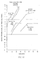
- the cross talk performance for a range of risetimes greater than twice the delay through the connector of the connector relative to other connector systems is best illustrated by a plot of the measured rise time-cross talk product (nanoseconds percent) versus signal density (signals/inch).
- the different signal densities correspond to different signal to ground ratio connections in the connector.
- the measured rise time-cross talk product of the scaled up 1,27 mm (.05") pitch model I-beam connector is shown in Fig. 18 for three signal to ground ratios; 1:1, 2:1, and all signals.
- the rise time cross talk product of the 0,635 mm (.025 inch) pitch I-beam connector for all signals is .75 and is much less than that of the other interconnects at correspondingly high signal to ground ratios.
- the rise time cross talk product of the .025 inch pitch I-beam connector for all signals is .75 and is much less than that of the other interconnects at correspondingly high signal to ground ratios.
- the rise time cross-talk product is independent of signal density for signal to ground ratios greater than 1:1.
- a dielectric may be extruded in an I-beam shape and a conductor may be positioned on that I-beam on the web and the horizontal flanges so as to achieve low cross talk as was described above.
- I-beam dielectric extrusions are shown at numerals 369 and 370.
- Each of these extensions has a web 371 which is perpendicularly interposed at its upper and lower edges between flanges as at 372 and 373.
- the flanges have inwardly facing interior surfaces and outwardly facing exterior surfaces which have metallized top ground planes sections 374 and 376 and metallized bottom ground plane sections respectively at 378 and 380.
- the webs also have conductive layers on their lateral sides.
- I-beam extrusion 370 has vertical signal lines 382 and 384 and I-beam extrusion 374 has vertical signal lines 386 and 388. These vertical signal lines and ground plane sections will preferably be metallized as for example, metal tape. It will be understood that the pair of vertical metallized sections on each extrusion will form one signal line.
- the property of the I-beam geometry as it relates to impedance and cross talk control will be generally the same as is discussed above in connection with the connector of the present invention.
- I-beam extrusions have interlocking steps as at 390 and 392 to maintain alignment of each I-beam element in the assembly.
- I-beam elements shown generally at 394, 396 and 398 are metallized (not shown) as described above and may be wrapped in a foil and elastic insulative jacket shown generally at numeral 400. Because of the regular alignment of the I-beam element in a collinear array, the I-beam cable assembly can be directly plugged to a receptacle without any fixturing of the cable except for removing the outer jacket of foil at the pluggable end.
- the receptacle can have contact beams which mate with blade elements made up of the ground and signal metallizations.
- the receptacle is shown generally at numeral 402 having signal contacts 404 and 406 received respectively vertical sections of I-beam elements 408 and 410.
- the receptacle also includes ground contacts 412 and 414 which contact respectively the metallized top ground plane sections 416 and 418. It is believed that for the cable assembly described above rise time cross-talk product will be independent of signal density for signal to ground ratios greater than 1:1.
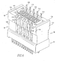
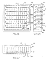
- the arrangement of dielectric and conductor elements in the I-beam geometry described herein is adapted for use in a ball grid array type electrical connector.
- a plug for use in such a connector is shown in Figs. 24 - 27 .
- the plug is shown generally at numeral 420.
- This plug includes a dielectric base section 422, a dielectric peripheral wall 424, metallic signal pins as at 426, 428, 430, 432 and 434 are arranged in a plurality of rows and extend perpendicularly upwardly from the base section. Longitudinally extending metallic grounding elements 436, 438, 440, 442, 444 and 446 are positioned between the rows of signal pins and extend perpendicularly from the base section.
- the plug also includes alignment and mounting pins 448 and 450. On its bottom side the plug also includes a plurality of rows of solder conductive tabs as at 452 and 454.
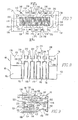
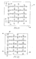
- a receptacle which mates with the plug 420 is shown generally at numeral 456.
- This receptacle includes a base section dielectric 458, a peripheral recess 460 and rows of metallic pin receiving recesses as at 462, 464, 466, 468 and 470.
- Metallic grounding elements receiving structures 472, 474, 476, 478, 480 and 482 are interposed between the rows of pin receiving recesses.
- the receptacle On its bottom side the receptacle also includes alignment and mounting pins 484 and 486
Description
-
- 1. Field of the Invention: The present invention relates to electrical connectors and more particularly to electrical connectors including means for controlling electrical cross talk and impedance.
- 2. Brief Description of Prior Developments: As the density of interconnects increases and the pitch between contacts approaches .5mm (.025 inches), the close proximity of the contacts increases the likelihood of strong electrical cross talk coupling between the contacts. In addition, maintaining design control over the electrical characteristic impedance of the contacts becomes increasingly difficult. In most interconnects, the mated plug/receptacle contact is surrounded by structural plastic with air spaces to provide mechanical clearances for the contact beam. As is disclosed in
U.S. Patent No. 5,046,960 to Fedder , these air spaces can be used to provide some control over the characteristic impedance of the mated contact. Heretofore, however, these air spaces have not been used, in conjunction with the plastic geometry, to control both impedance and, more importantly, cross talk. - Document
US 4,605,278 relates to solder-bearing lead useful as a terminal or contact, which may be fabricated by rapid progressive stamping techniques, for use with multiple contact connectors and electronic circuit boards. Document 4,679,889 is a continuation of the above mentionedUS 4,605,278 and relates to the same technology. - Document
JP 6243936 claim 1, for connecting for example printed circuit boards with each other. - In the connector of the present invention there is a plug member comprising a metallic contact means and a dielectric base means. The metallic contact means extend perpendicularly from the dielectric base means. The metallic contact means connects to form what is referred to herein as a generally "I-beam" shaped geometry. The concept behind the I-beam geometry is the use of strong dielectric loading through the structural dielectric to ground on the top and bottom of the mated contact edges and a relatively light loading through air on the mated contact sides. These different dielectric loadings are balanced in such a way as to maintain a controlled impedance and yet minimize coupling (and cross talk) between adjacent contacts. In this way, all lines of the interconnect can be dedicated to signals while maintaining a controlled impedance and a relatively low rise time-cross talk product of less than 1 nano-second percent. Typical rise time-cross talk values for existing 1,27 - 0,635 mm (.05 to .025 inch) pitch controlled impedance interconnects range from 2.5 to 4 nano-second percent.
- For connectors having the I-beam geometry of this invention, it is believed that rise time cross-talk product will be independent of signal density for signal to ground ratios greater than 1:1.
- The invention is further described with reference to the accompanying drawings in which:
-
Figs. 1-23 are explanatory examples for better understanding of the invention andFigs. 24-33 show an inventive example. -
Fig. 1 is a schematic illustration of the I-beam concept; -
Fig. 1a is a schematic illustration of the I-beam transmission geometry; -
Fig. 2 is a schematic illustration of another I-beam geometry; -
Fig. 3 is another schematic illustration of the I-beam geometry; -
Fig. 4 is a side elevational view of a connector; -
Fig. 5 is an end view of the connector shown inFig. 4 ; -
Fig. 6 is a perspective view of the connector shown inFig. 4 ; -
Fig. 7 is a bottom plan view of the receptacle element shown inFig. 4 ; -
Fig. 8 is an end view of the receptacle element of the connector shown inFig. 7 ; -
Fig. 9 is a cross sectional view taken through IX - IX inFig. 7 ; -
Fig. 10 is a bottom plan view of the receptacle element shown inFig. 4 ; -
Fig. 11 is an end view of the receptacle shown inFig. 10 ; -
Fig. 12 is a cross sectional view taken through XII - XII inFig. 10 ; -
Fig. 13 is a perspective view of the receptacle element shown inFig. 10 ; -
Fig. 14 is a cross sectional view of the plug and receptacle elements of the connector shown inFig. 4 prior to engagement; -
Fig. 15 is a cross sectional view; -
Fig. 16 is a cross sectional view corresponding toFig. 15 of another connector; -
Figs. 17 and18 are graphs illustrating the results of comparative tests described hereafter; -
Fig. 19 is a perspective view of a cable assembly; -
Fig. 20 is a detailed view of the area within circle XX inFig. 19 ; -
Fig. 21 is a schematic view of another cable assembly; -
Fig. 22 is a schematic side elevational view of a receptacle; -
Fig. 23 is a bottom plan view of the receptacle shown inFig. 22 . -
Fig. 24 is a top plan view of a plug section of an embodiment of the connector of the present invention; -
Fig. 25 is a bottom plan view of the plug section shown inFig. 24 ; -
Fig. 26 is an end view of the plug section shown inFig. 24 ; -
Fig. 27 is a side elevational view of the plug section shown inFig. 24 ; -
Fig. 28 is a top plan view of a receptacle section which is engageable with the plug section of the embodiment of the present invention shown inFig. 24 ; -
Fig. 29 is a bottom plan view of the receptacle shown inFig. 28 ; -
Fig. 30 is an end view of the receptacle shown inFig. 28 ; -
Fig. 31 is a side elevational view of the receptacle shown inFig. 28 ; -
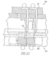
Fig. 32 is a fragmented cross sectional view as taken through lines XXXII-XXXII inFigs. 24 and28 showing those portions of the plug and receptacle shown in those drawings in an unengaged position; and -
Fig. 33 is a fragmented cross sectional view as would be shown as taken through lines XXXIII - XXXIII inFigs. 24 and28 if those elements were engaged. - The basic I-beam transmission line geometry is shown in
Fig. 1 . The description of this transmission line geometry as an I-beam comes from the vertical arrangement of the signal conductor shown generally atnumeral 10 between the two horizontal dielectric 12 and 14 having a dielectric constant ε andground planes sides air 24 having an air dielectric constant ε0. In a connector application the conductor would be comprised of twosections dielectric layers Fig. 1 . Thelines Fig. 1 are equipotentials of voltage in the air-dielectric space. Taking an equipotential line close to one of the ground planes and following it out towards the boundaries A and B, it will be seen that both boundary A are very close to the ground potential. This means that at both boundary A and boundary B we have virtual ground surfaces and if two or more I-beam modules are placed side by side, a virtual ground surface exists between the modules and there will be no coupling between the modules. In general, the conductor width wC and dielectric thickness should be small compared to the dielectric width or module pitch. - Given the mechanical constraints on a practical connector design, the proportioning of the signal conductor (blade/beam contact) width and dielectric thicknesses will, of necessity, deviate somewhat from the preferred ratios and some minimal coupling will exist between adjacent signal conductors. However, designs using the basic I-beam guidelines will have lower cross talk than more conventional approaches. Referring to
Fig. 1a , an alternate example is shown in which the dielectric is shown at 12' and 14' with their respective ground planes at 13' and 15'. In this embodiment the conductor 26' and 28' extend respectively from dielectric layers 12' and 14', but the conductors 26' and 28' abut side to side rather than end to end. An example of a practical electrical and mechanical I-beam design for a 0,635 mm (.025 inch) pitch connector uses 8 x 8 mil beams 26" and 8 x 8mil blades 28", which when mated, form an 8 x 16 mil signal contact and the contact cross-section is shown inFig. 2 . The dielectric thickness, t, is 12 mils. The voltage equipotentials for this geometry are shown inFig. 3 where virtual grounds are at the adjacent contact locations and some coupling will now exist between adjacent contacts. - Referring to
Fig. 2 , the I-beam transmission geometry is shown as being adapted to a less than ideally proportioned multi-conductor system.Signal conductors air spaces - Referring to
Fig. 3 , another multi-conductor connector is shown wherein there areparallel conductors air spaces - Referring particularly to
Figs. 4 to 12 it will be seen that the connector is generally comprised of a plug shown generally atnumeral 90 and a receptacle shown generally atnumeral 92. The plug consists of a preferably metallic plug housing 94 which has anarrow front section 96 and a widerear section 98. The front section has atop side 100 and abottom side 102. The wide rear section has atop side 104 and abottom side 106. The plug also hasend surfaces longitudinal grooves apertures transverse groove 132, while on the bottom side there is a similarly positioned bottomtransverse groove 134. The plug also hasrear standoffs Fig. 9 it will be seen that the plug includes adielectric element 140 which has a rearupward extension 142 and a reardownward extension 144 as well as a majorforward extension 146 and a minorforward extension 148. The housing also includes opposed downwardly extendingprojection 150 and upwardly extendingprojection 152 which assist in retaining the dielectric in its position. In the longitudinal grooves on the top side of the plug there are top axial ground springs 154, 156, 158, 160 and 162. In the transverse groove there is also a toptransverse ground spring 164. This transverse ground spring is fixed to the housing by means ofground spring fasteners top grounding contacts transverse ground spring 196 as with the top transverse ground spring, this spring is fixed in the housing by means ofground spring fasteners bottom ground contacts medial contact section 222 and arearward signal pin 224. An adjacent signal pin is shown at 226. Other signal pins are shown, for example, inFig. 7 at 228, 230, 232, 234 and 236. These pins pass through slots in the dielectric as at 238, 240, 242, 244, 246, 248 and 250. The dielectric is locked in place by means oflocks Fig. 9 the plug includes afront plug opening 260 and top and bottominterior plug walls Fig. 9 that a convex section of the ground springs as at 266 and 268 extend through the apertures in the longitudinal grooves. Referring particularly toFigs. 10 through 12 , it will be seen that the receptacle includes a preferablymetallic receptacle housing 270 with anarrow front section 272 and a widerrear section 274. The front section has a topside 276 and abottom side 278 and the rear section has a topside 280 and 282. The receptacle also has opposed ends 284 and 286. On the top sides of the receptacle there arelongitudinal grooves rear standoffs Fig. 12 , the receptacle includes a dielectric element shown generally at numeral 316 which has a rearupward extension 318, a reardownward extension 320, a majorforward extension 322 and a minorforward extension 324. The dielectric is retained in position by means of downward housing projection 326 and upward interior housing projection 328 along with rear retaining plate 330. Retained within each of the apertures there is a ground spring as at 332 which connects to atop ground post 334. Other top ground posts as at 336 and 338 are similarly positioned. Bottom ground springs as at 340 are connected to ground posts as at 342 while other ground posts as at 344 and 346 are positioned adjacent to similar ground springs. Referring particularly toFig. 12 , the receptacle also includes a metallic contact section shown generally at numeral 348 which has afront recess section 350, amedial contact section 352 and arearward signal pin 354. An adjacent pin is shown at 356. These pins extend rearwardly through slots as at 358 and 360. The dielectric is further retained in the housing by dielectric locks as at 362 and 364. The receptacle also includes afront opening 365 and aninterior housing surface 366. Referring particularly toFig. 13 , this perspective view of the receptacle shows the structure of themetallic contact section 350 in greater detail to reveal a plurality of alternating longitudinal ridges as at 367 andgrooves 368 as at which engage similar structures onmetallic contact 218 of the receptacle. - Referring particularly to
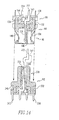
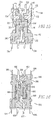
Figs. 14 and15 , the plug and receptacle are shown respectively in a disengaged and in an engaged configuration. It will be observed that the majorforward extension 146 of the dielectric section of the plug abuts the minor forward extension of the dielectric section of the receptacle end to end. The major forward extension of the dielectric section of the receptacle abuts the minor forward extension of the dielectric section of the plug end to end. It will also be observed on the metallic section of the plug the terminal recess receives the metallic element of the receptacle in side by side abutting relation. The terminal recess of the metallic contact element of the receptacle receives the metallic contact element of the plug in side by side abutting relation. The front end of the terminal housing abuts the inner wall of the plug. The ground springs of the plug also abut and make electrical contact with the approved front side walls of the receptacle. It will be noted that when the connector shown inFig. 15 where the plug and receptacle housings are axially engaged, the plug metallic contact and receptacle metallic contact extend axially inwardly respectively from the plug dielectric element and the receptacle dielectric element to abut each other. It will also be noted that the plug and receptacle dielectric elements extend radially outwardly respectfully from the plug and receptacle metallic contact elements. - Referring to
Fig. 16 , it will be seen that an alternate embodiment is generally comprised of a plug shown generally atnumerals 590 and a receptacle shown generally atnumerals 592. The plug consists of aplug housing 594. There is also aplug ground contact 596, plugground spring 598, plug signal pins 600 and 602,plug contact 606 anddielectric insert 608. The receptacle consists ofreceptacle housing 610,receptacle ground contact 612, receptacle ground springs 614 andreceptacle contact 616. Analignment frame 618 and receptacle signal pins 620 and 622 are also provided. It will be appreciated that this arrangement affords the same I-beam geometry as was described above. - The measured near end (NEXT) and far end (FEXT) cross talk at the rise time of 35p sec, for a 0,635 mm (.05") pitch scaled up model of a connector made according to the foregoing first described embodiment are shown in
Fig. 17 . The valley in the NEXT wave form of approximately 7% is the near end cross talk arising in the I-beam section of the connector. The leading and trailing peaks come from cross talk at the input and output sections of the connector where the I-beam geometry cannot be maintained because of mechanical constraints. - The cross talk performance for a range of risetimes greater than twice the delay through the connector of the connector relative to other connector systems is best illustrated by a plot of the measured rise time-cross talk product (nanoseconds percent) versus signal density (signals/inch). The different signal densities correspond to different signal to ground ratio connections in the connector. The measured rise time-cross talk product of the scaled up 1,27 mm (.05") pitch model I-beam connector is shown in
Fig. 18 for three signal to ground ratios; 1:1, 2:1, and all signals. Since the cross talk of the scaled up model is twice that of the 0,635 mm (.025 inch) design, the performance of the 0,635 mm (.025 inch) pitch, single row design is easily extrapolated to twice the density and one half the model cross talk. For the two row design, the density is four times that of the model and the cross talk is again one half. The extrapolated performance of the one row and two row 0,635 mm (.025 inch) pitch connectors are also shown inFig. 18 relative to that of a number of conventional connectors as are identified in that figure. The rise time cross talk product of the 0,635 mm (.025 inch) pitch I-beam connector for all signals is .75 and is much less than that of the other interconnects at correspondingly high signal to ground ratios. Referring particularly to the 0,635 mm (.05 inch) pitch model curve inFig. 18 , it will beFig. 18 relative to that of a number of conventional connectors as are identified in that figure. The rise time cross talk product of the .025 inch pitch I-beam connector for all signals is .75 and is much less than that of the other interconnects at correspondingly high signal to ground ratios. Referring particularly to the .05 inch pitch model curve inFig. 18 , it will be observed that the rise time cross-talk product is independent of signal density for signal to ground ratios greater than 1:1. - Referring to
Figs. 19 and 20 , it will be seen that the beneficial results achieved may also be achieved in a cable assembly. That is, a dielectric may be extruded in an I-beam shape and a conductor may be positioned on that I-beam on the web and the horizontal flanges so as to achieve low cross talk as was described above. I-beam dielectric extrusions are shown atnumerals web 371 which is perpendicularly interposed at its upper and lower edges between flanges as at 372 and 373. The flanges have inwardly facing interior surfaces and outwardly facing exterior surfaces which have metallized topground planes sections beam extrusion 370 hasvertical signal lines beam extrusion 374 hasvertical signal lines Fig. 20 , it will be seen that the I-beam extrusions have interlocking steps as at 390 and 392 to maintain alignment of each I-beam element in the assembly. Referring toFig. 21 , I-beam elements shown generally at 394, 396 and 398 are metallized (not shown) as described above and may be wrapped in a foil and elastic insulative jacket shown generally atnumeral 400. Because of the regular alignment of the I-beam element in a collinear array, the I-beam cable assembly can be directly plugged to a receptacle without any fixturing of the cable except for removing the outer jacket of foil at the pluggable end. The receptacle can have contact beams which mate with blade elements made up of the ground and signal metallizations. Referring particularly toFig. 22 , it will be seen, for example, that the receptacle is shown generally at numeral 402 havingsignal contacts 404 and 406 received respectively vertical sections of I-beam elements Fig. 23 , the receptacle also includesground contacts ground plane sections - In the following a connector according to the invention will be described:
- The arrangement of dielectric and conductor elements in the I-beam geometry described herein is adapted for use in a ball grid array type electrical connector. A plug for use in such a connector is shown in
Figs. 24 - 27 . Referring to these figures, the plug is shown generally atnumeral 420. This plug includes adielectric base section 422, a dielectricperipheral wall 424, metallic signal pins as at 426, 428, 430, 432 and 434 are arranged in a plurality of rows and extend perpendicularly upwardly from the base section. Longitudinally extendingmetallic grounding elements pins - Referring to
Figs. 28 - 31 , a receptacle which mates with theplug 420 is shown generally atnumeral 456. This receptacle includes abase section dielectric 458, aperipheral recess 460 and rows of metallic pin receiving recesses as at 462, 464, 466, 468 and 470. Metallic groundingelements receiving structures pins - An electrical connector has been described which by virtue of its I-beam shaped geometry allows for low cross talk and impedance control.
- Also an electrical cable has been described which affords low cross talk and impedance control by reason of this same geometry.
- While the present invention has been described in connection with the preferred embodiments of
Figures 24-27 ,32 and33 , it is to be understood that other similar embodiments may be used or modifications and additions may be made to the described embodiment for performing the same function of the present invention without deviating therefrom. Therefore, the present invention should not be limited to any single embodiment, but rather construed in scope of the appended claims.
Claims (2)
- An electrical connector comprising:a) a plug member (420) including a dielectric base section (422) and a dielectric peripheral wall (424) extending perpendicular from the dielectric base section (422) in mating direction of the plug member (420);b) metallic pins (426, 428, 430, 432, 434) arranged in a plurality of rows, which metallic pins (426, 428, 430, 432, 434) are carried by said dielectric base section (422) and extend perpendicularly thereto; andc) longitudinally extending grounding elements ((436, 438, 440, 442, 444, 446) positioned between said rows of metallic pins (426, 428, 430, 432, 434) and extending perpendicularly to said dielectric base section (422);d) said metallic pins (426, 428, 430, 432, 434) each comprising a mating end and a mounting end opposite said mating end, whereby the mating end extends beyond said dielectric base section;
characterized in thate) solder balls (452, 454) are attached to said metallic pins (426, 428, 430, 432, 434) and spaced from said dielectric base section (422), such that said solder balls (452, 454) extend beyond said dielectric base section (422) and form a ball grid array; wherebyf) said mounting ends of said metallic pins (426, 428 430, 432, 434) each have a free end and said solder balls (452, 454) are positioned adjacent to said free ends of said metallic pins (426, 428, 430, 432, 434). - The electrical connector as claimed in claim 1, wherein said mounting end of each of said metallic pins (426, 428, 430, 432, 434) is bent at an angle of about 90° with respect to said mating end of said metallic pins (426, 428, 430, 432, 434).
Applications Claiming Priority (3)
| Application Number | Priority Date | Filing Date | Title |
|---|---|---|---|
| US45202095A | 1995-06-12 | 1995-06-12 | |
| US08/452,021 US5817973A (en) | 1995-06-12 | 1995-06-12 | Low cross talk and impedance controlled electrical cable assembly |
| EP96919391A EP0836757B1 (en) | 1995-06-12 | 1996-06-11 | Low cross talk and impedance controlled electrical connector |
Related Parent Applications (1)
| Application Number | Title | Priority Date | Filing Date |
|---|---|---|---|
| EP96919391A Division EP0836757B1 (en) | 1995-06-12 | 1996-06-11 | Low cross talk and impedance controlled electrical connector |
Publications (2)
| Publication Number | Publication Date |
|---|---|
| EP1717912A1 EP1717912A1 (en) | 2006-11-02 |
| EP1717912B1 true EP1717912B1 (en) | 2015-04-08 |
Family
ID=27036615
Family Applications (5)
| Application Number | Title | Priority Date | Filing Date |
|---|---|---|---|
| EP06007279A Expired - Lifetime EP1679765B1 (en) | 1995-06-12 | 1996-06-11 | Low cross talk and impedance controlled electrical connector |
| EP06007278.2A Expired - Lifetime EP1679770B1 (en) | 1995-06-12 | 1996-06-11 | Low cross talk and impedance controlled electrical connector |
| EP96919391A Expired - Lifetime EP0836757B1 (en) | 1995-06-12 | 1996-06-11 | Low cross talk and impedance controlled electrical connector |
| EP06007681.7A Expired - Lifetime EP1717912B1 (en) | 1995-06-12 | 1996-06-11 | Low cross talk and impedance controlled electrical connector |
| EP05014163A Expired - Lifetime EP1594184B1 (en) | 1995-06-12 | 1996-06-11 | Low cross talk and impedance controlled electrical connector and electrical cable assembly |
Family Applications Before (3)
| Application Number | Title | Priority Date | Filing Date |
|---|---|---|---|
| EP06007279A Expired - Lifetime EP1679765B1 (en) | 1995-06-12 | 1996-06-11 | Low cross talk and impedance controlled electrical connector |
| EP06007278.2A Expired - Lifetime EP1679770B1 (en) | 1995-06-12 | 1996-06-11 | Low cross talk and impedance controlled electrical connector |
| EP96919391A Expired - Lifetime EP0836757B1 (en) | 1995-06-12 | 1996-06-11 | Low cross talk and impedance controlled electrical connector |
Family Applications After (1)
| Application Number | Title | Priority Date | Filing Date |
|---|---|---|---|
| EP05014163A Expired - Lifetime EP1594184B1 (en) | 1995-06-12 | 1996-06-11 | Low cross talk and impedance controlled electrical connector and electrical cable assembly |
Country Status (9)
| Country | Link |
|---|---|
| US (1) | US6210182B1 (en) |
| EP (5) | EP1679765B1 (en) |
| JP (4) | JP4128624B2 (en) |
| KR (2) | KR100408176B1 (en) |
| CN (2) | CN1148843C (en) |
| AU (1) | AU6174196A (en) |
| CA (1) | CA2224519C (en) |
| DE (2) | DE69636779T2 (en) |
| WO (1) | WO1996042123A1 (en) |
Families Citing this family (46)
| Publication number | Priority date | Publication date | Assignee | Title |
|---|---|---|---|---|
| US6024584A (en) * | 1996-10-10 | 2000-02-15 | Berg Technology, Inc. | High density connector |
| US6093035A (en) * | 1996-06-28 | 2000-07-25 | Berg Technology, Inc. | Contact for use in an electrical connector |
| EP1441417A3 (en) * | 1996-10-10 | 2004-12-01 | Fci | High density connector and method of manufacture |
| SG71046A1 (en) | 1996-10-10 | 2000-03-21 | Connector Systems Tech Nv | High density connector and method of manufacture |
| US6139336A (en) | 1996-11-14 | 2000-10-31 | Berg Technology, Inc. | High density connector having a ball type of contact surface |
| US6183301B1 (en) | 1997-01-16 | 2001-02-06 | Berg Technology, Inc. | Surface mount connector with integrated PCB assembly |
| EP1053571A4 (en) * | 1998-01-08 | 2001-03-28 | Berg Electronics Mfg | High speed connector |
| DE69902491T2 (en) * | 1998-02-27 | 2003-04-10 | Lucent Technologies Inc | Low crosstalk connector |
| US6869292B2 (en) * | 2001-07-31 | 2005-03-22 | Fci Americas Technology, Inc. | Modular mezzanine connector |
| US6692272B2 (en) * | 2001-11-14 | 2004-02-17 | Fci Americas Technology, Inc. | High speed electrical connector |
| SG98466A1 (en) * | 2001-12-28 | 2003-09-19 | Fci Asia Technology Pte Ltd | An electrical connector |
| US7130921B2 (en) * | 2002-03-15 | 2006-10-31 | International Business Machines Corporation | Centrally enhanced peer-to-peer resource sharing method and apparatus |
| US6979238B1 (en) | 2004-06-28 | 2005-12-27 | Samtec, Inc. | Connector having improved contacts with fusible members |
| US7976345B2 (en) * | 2005-12-15 | 2011-07-12 | Tyco Electronics Corporation | Electrical contact assembly and method of manufacturing thereof |
| JP4550733B2 (en) * | 2005-12-20 | 2010-09-22 | ヒロセ電機株式会社 | Electrical connector |
| TWI463750B (en) * | 2006-12-19 | 2014-12-01 | Fci Americas Technology Inc | Shieldless, high-speed, low-cross-talk electrical connector |
| JP4862796B2 (en) * | 2007-09-28 | 2012-01-25 | 山一電機株式会社 | High-density connector for high-speed transmission |
| US8366485B2 (en) | 2009-03-19 | 2013-02-05 | Fci Americas Technology Llc | Electrical connector having ribbed ground plate |
| CN107069274B (en) | 2010-05-07 | 2020-08-18 | 安费诺有限公司 | High performance cable connector |
| US8597036B2 (en) * | 2010-07-19 | 2013-12-03 | Tyco Electronics Corporation | Transceiver assembly |
| JP5605378B2 (en) * | 2012-01-18 | 2014-10-15 | Smk株式会社 | Electrical connector |
| EP2624034A1 (en) | 2012-01-31 | 2013-08-07 | Fci | Dismountable optical coupling device |
| US8944831B2 (en) | 2012-04-13 | 2015-02-03 | Fci Americas Technology Llc | Electrical connector having ribbed ground plate with engagement members |
| USD727268S1 (en) | 2012-04-13 | 2015-04-21 | Fci Americas Technology Llc | Vertical electrical connector |
| USD727852S1 (en) | 2012-04-13 | 2015-04-28 | Fci Americas Technology Llc | Ground shield for a right angle electrical connector |
| USD718253S1 (en) | 2012-04-13 | 2014-11-25 | Fci Americas Technology Llc | Electrical cable connector |
| US9257778B2 (en) | 2012-04-13 | 2016-02-09 | Fci Americas Technology | High speed electrical connector |
| US9543703B2 (en) | 2012-07-11 | 2017-01-10 | Fci Americas Technology Llc | Electrical connector with reduced stack height |
| USD751507S1 (en) | 2012-07-11 | 2016-03-15 | Fci Americas Technology Llc | Electrical connector |
| CN104704682B (en) | 2012-08-22 | 2017-03-22 | 安费诺有限公司 | High-frequency electrical connector |
| USD745852S1 (en) | 2013-01-25 | 2015-12-22 | Fci Americas Technology Llc | Electrical connector |
| USD720698S1 (en) | 2013-03-15 | 2015-01-06 | Fci Americas Technology Llc | Electrical cable connector |
| US9450344B2 (en) | 2014-01-22 | 2016-09-20 | Amphenol Corporation | High speed, high density electrical connector with shielded signal paths |
| US9692183B2 (en) * | 2015-01-20 | 2017-06-27 | Te Connectivity Corporation | Receptacle connector with ground bus |
| WO2017007429A1 (en) | 2015-07-07 | 2017-01-12 | Amphenol Fci Asia Pte. Ltd. | Electrical connector |
| CN113690654A (en) * | 2016-06-15 | 2021-11-23 | 申泰公司 | Overmolded lead frame providing contact support and impedance matching characteristics |
| WO2018039164A1 (en) | 2016-08-23 | 2018-03-01 | Amphenol Corporation | Connector configurable for high performance |
| US11668198B2 (en) | 2018-08-03 | 2023-06-06 | Raytheon Technologies Corporation | Fiber-reinforced self-healing environmental barrier coating |
| US11535571B2 (en) | 2018-08-16 | 2022-12-27 | Raytheon Technologies Corporation | Environmental barrier coating for enhanced resistance to attack by molten silicate deposits |
| US11505506B2 (en) | 2018-08-16 | 2022-11-22 | Raytheon Technologies Corporation | Self-healing environmental barrier coating |
| CN208862209U (en) | 2018-09-26 | 2019-05-14 | 安费诺东亚电子科技(深圳)有限公司 | A kind of connector and its pcb board of application |
| CN115428275A (en) | 2020-01-27 | 2022-12-02 | 富加宜(美国)有限责任公司 | High speed connector |
| WO2021154718A1 (en) | 2020-01-27 | 2021-08-05 | Fci Usa Llc | High speed, high density direct mate orthogonal connector |
| JP7453851B2 (en) * | 2020-05-26 | 2024-03-21 | 株式会社アドバンテスト | Coaxial terminals, coaxial connectors, wiring boards, and electronic component testing equipment |
| CN215816516U (en) | 2020-09-22 | 2022-02-11 | 安费诺商用电子产品(成都)有限公司 | Electrical connector |
| CN213636403U (en) | 2020-09-25 | 2021-07-06 | 安费诺商用电子产品(成都)有限公司 | Electrical connector |
Family Cites Families (61)
| Publication number | Priority date | Publication date | Assignee | Title |
|---|---|---|---|---|
| GB1129150A (en) | 1965-12-03 | 1968-10-02 | Ass Elect Ind | Improvements relating to electric cables |
| US3571488A (en) | 1969-04-11 | 1971-03-16 | Federal Pacific Electric Co | Enclosed bus duct |
| US3708606A (en) | 1970-05-13 | 1973-01-02 | Air Reduction | Cryogenic system including variations of hollow superconducting wire |
| US3763306A (en) * | 1972-03-17 | 1973-10-02 | Thomas & Betts Corp | Flat multi-signal transmission line cable with plural insulation |
| US3871728A (en) | 1973-11-30 | 1975-03-18 | Itt | Matched impedance printed circuit board connector |
| US4368942A (en) | 1977-02-11 | 1983-01-18 | Bunker Ramo Corporation | Keyed connector to prevent intermating with a standard connector |
| DE2711531C3 (en) | 1977-03-16 | 1979-10-11 | Siemens Ag, 1000 Berlin Und 8000 Muenchen | Cable for low-crosstalk transmission of small signals |
| US4403103A (en) | 1980-11-14 | 1983-09-06 | Westinghouse Electric Corp. | Gas-insulated transmission line having improved outer enclosure |
| US4605278A (en) * | 1985-05-24 | 1986-08-12 | North American Specialties Corporation | Solder-bearing leads |
| USRE32691E (en) | 1982-08-23 | 1988-06-07 | Amp Incorporated | High speed modular connector for printed circuit boards |
| US4605915A (en) | 1984-07-09 | 1986-08-12 | Cubic Corporation | Stripline circuits isolated by adjacent decoupling strip portions |
| US4678250A (en) | 1985-01-08 | 1987-07-07 | Methode Electronics, Inc. | Multi-pin electrical header |
| US4695106A (en) | 1985-05-13 | 1987-09-22 | Amp Incorporated | Surface mount, miniature connector |
| US4593341A (en) * | 1985-05-22 | 1986-06-03 | Corning Glass Works | Tubular capacitor end terminations |
| US4767344A (en) | 1986-08-22 | 1988-08-30 | Burndy Corporation | Solder mounting of electrical contacts |
| US5169324A (en) * | 1986-11-18 | 1992-12-08 | Lemke Timothy A | Plug terminator having a grounding member |
| US4836791A (en) | 1987-11-16 | 1989-06-06 | Amp Incorporated | High density coax connector |
| JPS63249394A (en) | 1987-04-06 | 1988-10-17 | 日本電気株式会社 | Multilayer circuit board |
| US4773878A (en) * | 1987-07-02 | 1988-09-27 | W. L. Gore & Associates | Shielded flat cable connectors |
| US4785135A (en) * | 1987-07-13 | 1988-11-15 | International Business Machines Corporation | De-coupled printed circuits |
| DE3884708T2 (en) * | 1987-07-28 | 1994-05-05 | Whitaker Corp | Wire replacement connector assembly for use with printed circuit boards. |
| US4798918A (en) * | 1987-09-21 | 1989-01-17 | Intel Corporation | High density flexible circuit |
| JPH01246713A (en) | 1988-03-28 | 1989-10-02 | Junkosha Co Ltd | Flat cable |
| JPH0614326Y2 (en) | 1988-10-24 | 1994-04-13 | 住友電気工業株式会社 | Flat cable with shield |
| US5038252A (en) | 1989-01-26 | 1991-08-06 | Teradyne, Inc. | Printed circuit boards with improved electrical current control |
| CA2011393A1 (en) * | 1989-03-31 | 1990-09-30 | Wayne S. Davis | Back-to-back stackable connector for interface bus |
| US4932888A (en) | 1989-06-16 | 1990-06-12 | Augat Inc. | Multi-row box connector |
| ES2070283T3 (en) | 1989-10-10 | 1995-06-01 | Whitaker Corp | CONTRAPLANE CONNECTOR WITH ADAPTED IMPEDANCES. |
| DE3936466C2 (en) * | 1989-11-02 | 1994-06-09 | Erni Elektroapp | Multi-pole high-frequency connector |
| US5036160A (en) | 1989-11-07 | 1991-07-30 | Crosspoint Systems, Inc. | Twisted pair backplane |
| SU1753519A1 (en) | 1990-02-05 | 1992-08-07 | Конструкторское бюро приборостроения Научно-производственного объединения "Точность" | Method for producing strip transmission line with strip conductors located normal to metal substrates |
| NL9000578A (en) * | 1990-03-14 | 1991-10-01 | Burndy Electra Nv | CONNECTOR ASSEMBLY FOR PRINT CARDS. |
| DE69114748T2 (en) | 1990-04-02 | 1996-06-05 | Whitaker Corp | Connectors mounted on a surface. |
| JPH088552Y2 (en) | 1990-05-29 | 1996-03-06 | モレックス インコーポレーテッド | Narrow pitch board to board electrical connector |
| US5055069A (en) * | 1990-06-08 | 1991-10-08 | E. I. Du Pont De Nemours And Company | Connectors with ground structure |
| US5133679A (en) | 1990-06-08 | 1992-07-28 | E. I. Du Pont De Nemours And Company | Connectors with ground structure |
| US5104329A (en) * | 1990-09-21 | 1992-04-14 | Amp Incorporated | Electrical connector assembly |
| JP2739608B2 (en) * | 1990-11-15 | 1998-04-15 | 日本エー・エム・ピー株式会社 | Multi-contact type connector for signal transmission |
| US5046960A (en) | 1990-12-20 | 1991-09-10 | Amp Incorporated | High density connector system |
| US5094623A (en) | 1991-04-30 | 1992-03-10 | Thomas & Betts Corporation | Controlled impedance electrical connector |
| EP0514055B1 (en) | 1991-05-13 | 1997-01-02 | Fujitsu Limited | Impedance-matched electrical connector |
| US5258648A (en) | 1991-06-27 | 1993-11-02 | Motorola, Inc. | Composite flip chip semiconductor device with an interposer having test contacts formed along its periphery |
| US5120232A (en) | 1991-08-06 | 1992-06-09 | Amp Incorporated | Electrical connector having improved grounding bus bars |
| US5181855A (en) | 1991-10-03 | 1993-01-26 | Itt Corporation | Simplified contact connector system |
| US5174764A (en) | 1991-12-20 | 1992-12-29 | Amp Incorporated | Connector assembly having surface mounted terminals |
| US5306196A (en) | 1992-01-30 | 1994-04-26 | Nec Corporation | Electric circuit board unit and electric connector and use therein |
| GB9205087D0 (en) | 1992-03-09 | 1992-04-22 | Amp Holland | Sheilded back plane connector |
| JPH05275139A (en) * | 1992-03-25 | 1993-10-22 | Toshiba Corp | Connector |
| US5215473A (en) * | 1992-05-05 | 1993-06-01 | Molex Incorporated | High speed guarded cavity backplane connector |
| EP0578880A1 (en) * | 1992-07-14 | 1994-01-19 | General Electric Company | Plated D-shell connector |
| US5226835A (en) * | 1992-08-06 | 1993-07-13 | At&T Bell Laboratories | Patch plug for cross-connect equipment |
| US5267881A (en) | 1992-09-24 | 1993-12-07 | Hirose Electric Co., Ltd. | Electrical connector |
| US5357050A (en) | 1992-11-20 | 1994-10-18 | Ast Research, Inc. | Apparatus and method to reduce electromagnetic emissions in a multi-layer circuit board |
| US5469130A (en) | 1992-11-27 | 1995-11-21 | Murata Mfg. Co., Ltd. | High frequency parallel strip line cable comprising connector part and connector provided on substrate for connecting with connector part thereof |
| JP3241139B2 (en) | 1993-02-04 | 2001-12-25 | 三菱電機株式会社 | Film carrier signal transmission line |
| JP3108239B2 (en) * | 1993-02-19 | 2000-11-13 | 富士通株式会社 | Impedance matched electrical connector |
| JP2961711B2 (en) * | 1993-05-21 | 1999-10-12 | 株式会社テクセル | Zipper connector |
| NL9300971A (en) | 1993-06-04 | 1995-01-02 | Framatome Connectors Belgium | Circuit board connector assembly. |
| JPH0794248A (en) * | 1993-09-24 | 1995-04-07 | Kel Corp | Electric connector |
| US5593322A (en) | 1995-01-17 | 1997-01-14 | Dell Usa, L.P. | Leadless high density connector |
| TW267265B (en) * | 1995-06-12 | 1996-01-01 | Connector Systems Tech Nv | Low cross talk and impedance controlled electrical connector |
-
1996
- 1996-06-11 CA CA002224519A patent/CA2224519C/en not_active Expired - Lifetime
- 1996-06-11 EP EP06007279A patent/EP1679765B1/en not_active Expired - Lifetime
- 1996-06-11 EP EP06007278.2A patent/EP1679770B1/en not_active Expired - Lifetime
- 1996-06-11 EP EP96919391A patent/EP0836757B1/en not_active Expired - Lifetime
- 1996-06-11 JP JP50330597A patent/JP4128624B2/en not_active Expired - Lifetime
- 1996-06-11 CN CNB961947675A patent/CN1148843C/en not_active Expired - Lifetime
- 1996-06-11 DE DE69636779T patent/DE69636779T2/en not_active Expired - Lifetime
- 1996-06-11 WO PCT/US1996/010210 patent/WO1996042123A1/en active IP Right Grant
- 1996-06-11 DE DE69638068T patent/DE69638068D1/en not_active Expired - Lifetime
- 1996-06-11 EP EP06007681.7A patent/EP1717912B1/en not_active Expired - Lifetime
- 1996-06-11 US US08/981,063 patent/US6210182B1/en not_active Expired - Lifetime
- 1996-06-11 CN CNB200410007330XA patent/CN1314170C/en not_active Expired - Lifetime
- 1996-06-11 EP EP05014163A patent/EP1594184B1/en not_active Expired - Lifetime
- 1996-06-11 AU AU61741/96A patent/AU6174196A/en not_active Abandoned
-
1997
- 1997-12-11 KR KR10-1997-0709303A patent/KR100408176B1/en not_active IP Right Cessation
-
2003
- 2003-06-10 JP JP2003164857A patent/JP2004006373A/en not_active Withdrawn
- 2003-08-14 KR KR10-2003-7010757A patent/KR100408175B1/en not_active IP Right Cessation
-
2006
- 2006-05-17 JP JP2006137766A patent/JP4409538B2/en not_active Expired - Lifetime
-
2008
- 2008-03-13 JP JP2008064129A patent/JP2008218416A/en not_active Withdrawn
Also Published As
| Publication number | Publication date |
|---|---|
| EP1679765B1 (en) | 2012-04-25 |
| CA2224519C (en) | 2002-05-07 |
| EP1594184A2 (en) | 2005-11-09 |
| KR100408176B1 (en) | 2004-02-18 |
| EP1717912A1 (en) | 2006-11-02 |
| DE69636779T2 (en) | 2007-10-18 |
| EP0836757A4 (en) | 1999-11-03 |
| JP4409538B2 (en) | 2010-02-03 |
| EP1594184A3 (en) | 2005-12-14 |
| MX9710073A (en) | 1998-10-31 |
| EP1594184B1 (en) | 2009-11-04 |
| JP4128624B2 (en) | 2008-07-30 |
| JP2008218416A (en) | 2008-09-18 |
| US6210182B1 (en) | 2001-04-03 |
| CA2224519A1 (en) | 1996-12-27 |
| EP1679765A3 (en) | 2006-07-19 |
| CN1189249A (en) | 1998-07-29 |
| EP1679765A2 (en) | 2006-07-12 |
| EP0836757B1 (en) | 2006-12-20 |
| CN1531153A (en) | 2004-09-22 |
| JPH11507763A (en) | 1999-07-06 |
| EP1679770A2 (en) | 2006-07-12 |
| EP1679770A3 (en) | 2006-07-26 |
| EP0836757A1 (en) | 1998-04-22 |
| KR100408175B1 (en) | 2003-12-01 |
| AU6174196A (en) | 1997-01-09 |
| CN1314170C (en) | 2007-05-02 |
| DE69636779D1 (en) | 2007-02-01 |
| DE69638068D1 (en) | 2009-12-17 |
| EP1679770B1 (en) | 2013-08-21 |
| JP2004006373A (en) | 2004-01-08 |
| WO1996042123A1 (en) | 1996-12-27 |
| CN1148843C (en) | 2004-05-05 |
| JP2006269440A (en) | 2006-10-05 |
Similar Documents
| Publication | Publication Date | Title |
|---|---|---|
| EP1717912B1 (en) | Low cross talk and impedance controlled electrical connector | |
| US6476316B1 (en) | Low cross talk and impedance controlled electrical cable assembly | |
| US5741144A (en) | Low cross and impedance controlled electric connector | |
| US6939173B1 (en) | Low cross talk and impedance controlled electrical connector with solder masses | |
| US5664968A (en) | Connector assembly with shielded modules | |
| US6371773B1 (en) | High density interconnect system and method | |
| US5104329A (en) | Electrical connector assembly | |
| US6129592A (en) | Connector assembly having terminal modules | |
| US6652318B1 (en) | Cross-talk canceling technique for high speed electrical connectors | |
| CA2037798C (en) | Connector assembly for printed circuit boards | |
| EP0634817B1 (en) | Shielded compact data connector | |
| US5306171A (en) | Bowtie connector with additional leaf contacts | |
| US5860814A (en) | Electric connector for printed circuit board | |
| US5603634A (en) | Small pitch dual row leaf connector | |
| JPH04229573A (en) | Connector with earthing structure | |
| US6814620B1 (en) | Electrical connector | |
| US6866518B1 (en) | Electrical interconnection between multiple printed circuit boards | |
| US6918775B2 (en) | Method for interconnecting multiple printed circuit boards | |
| US6918774B2 (en) | Electrical connector having long circuit boards | |
| JP3990355B2 (en) | Impedance adjusted high density connector | |
| EP0907219B1 (en) | Punched sheet coax header | |
| US6923655B2 (en) | Electrical connector for interconnecting two intersected printed circuit boards | |
| CN114530732A (en) | Differential signal connector | |
| MXPA97010073A (en) | Assembly of electrical connector and electric cable with controlled impedance and low diafo |
Legal Events
| Date | Code | Title | Description |
|---|---|---|---|
| PUAI | Public reference made under article 153(3) epc to a published international application that has entered the european phase |
Free format text: ORIGINAL CODE: 0009012 |
|
| AC | Divisional application: reference to earlier application |
Ref document number: 0836757 Country of ref document: EP Kind code of ref document: P |
|
| AK | Designated contracting states |
Kind code of ref document: A1 Designated state(s): DE FR GB |
|
| 17P | Request for examination filed |
Effective date: 20070502 |
|
| AKX | Designation fees paid |
Designated state(s): DE FR GB |
|
| 17Q | First examination report despatched |
Effective date: 20090310 |
|
| RAP1 | Party data changed (applicant data changed or rights of an application transferred) |
Owner name: FCI |
|
| REG | Reference to a national code |
Ref country code: DE Ref legal event code: R079 Ref document number: 69638689 Country of ref document: DE Free format text: PREVIOUS MAIN CLASS: H01R0043020000 Ipc: H01R0012710000 |
|
| GRAP | Despatch of communication of intention to grant a patent |
Free format text: ORIGINAL CODE: EPIDOSNIGR1 |
|
| GRAJ | Information related to disapproval of communication of intention to grant by the applicant or resumption of examination proceedings by the epo deleted |
Free format text: ORIGINAL CODE: EPIDOSDIGR1 |
|
| RIC1 | Information provided on ipc code assigned before grant |
Ipc: H01P 3/08 20060101ALI20141009BHEP Ipc: H01R 13/6461 20110101ALI20141009BHEP Ipc: H01R 12/71 20110101AFI20141009BHEP Ipc: H01R 43/02 20060101ALI20141009BHEP Ipc: H01R 13/6471 20110101ALI20141009BHEP |
|
| GRAP | Despatch of communication of intention to grant a patent |
Free format text: ORIGINAL CODE: EPIDOSNIGR1 |
|
| INTG | Intention to grant announced |
Effective date: 20141024 |
|
| INTG | Intention to grant announced |
Effective date: 20141114 |
|
| GRAS | Grant fee paid |
Free format text: ORIGINAL CODE: EPIDOSNIGR3 |
|
| GRAA | (expected) grant |
Free format text: ORIGINAL CODE: 0009210 |
|
| AC | Divisional application: reference to earlier application |
Ref document number: 0836757 Country of ref document: EP Kind code of ref document: P |
|
| AK | Designated contracting states |
Kind code of ref document: B1 Designated state(s): DE FR GB |
|
| RAP1 | Party data changed (applicant data changed or rights of an application transferred) |
Owner name: FCI ASIA PTE. LTD. |
|
| REG | Reference to a national code |
Ref country code: GB Ref legal event code: FG4D |
|
| REG | Reference to a national code |
Ref country code: DE Ref legal event code: R096 Ref document number: 69638689 Country of ref document: DE Effective date: 20150513 |
|
| PGFP | Annual fee paid to national office [announced via postgrant information from national office to epo] |
Ref country code: DE Payment date: 20150331 Year of fee payment: 20 |
|
| PGFP | Annual fee paid to national office [announced via postgrant information from national office to epo] |
Ref country code: GB Payment date: 20150731 Year of fee payment: 20 |
|
| REG | Reference to a national code |
Ref country code: DE Ref legal event code: R097 Ref document number: 69638689 Country of ref document: DE |
|
| PLBE | No opposition filed within time limit |
Free format text: ORIGINAL CODE: 0009261 |
|
| STAA | Information on the status of an ep patent application or granted ep patent |
Free format text: STATUS: NO OPPOSITION FILED WITHIN TIME LIMIT |
|
| 26N | No opposition filed |
Effective date: 20160111 |
|
| REG | Reference to a national code |
Ref country code: FR Ref legal event code: ST Effective date: 20160229 |
|
| PG25 | Lapsed in a contracting state [announced via postgrant information from national office to epo] |
Ref country code: FR Free format text: LAPSE BECAUSE OF NON-PAYMENT OF DUE FEES Effective date: 20150630 |
|
| REG | Reference to a national code |
Ref country code: DE Ref legal event code: R071 Ref document number: 69638689 Country of ref document: DE |
|
| REG | Reference to a national code |
Ref country code: GB Ref legal event code: PE20 Expiry date: 20160610 |
|
| PG25 | Lapsed in a contracting state [announced via postgrant information from national office to epo] |
Ref country code: GB Free format text: LAPSE BECAUSE OF EXPIRATION OF PROTECTION Effective date: 20160610 |