EP1724851A1 - Organic electrically bistable material and its use for producing a memory switch - Google Patents
Organic electrically bistable material and its use for producing a memory switch Download PDFInfo
- Publication number
- EP1724851A1 EP1724851A1 EP05020196A EP05020196A EP1724851A1 EP 1724851 A1 EP1724851 A1 EP 1724851A1 EP 05020196 A EP05020196 A EP 05020196A EP 05020196 A EP05020196 A EP 05020196A EP 1724851 A1 EP1724851 A1 EP 1724851A1
- Authority
- EP
- European Patent Office
- Prior art keywords
- alkyl
- group
- cation
- memory switch
- aralkyl
- Prior art date
- Legal status (The legal status is an assumption and is not a legal conclusion. Google has not performed a legal analysis and makes no representation as to the accuracy of the status listed.)
- Withdrawn
Links
Images


Classifications
-
- B—PERFORMING OPERATIONS; TRANSPORTING
- B82—NANOTECHNOLOGY
- B82Y—SPECIFIC USES OR APPLICATIONS OF NANOSTRUCTURES; MEASUREMENT OR ANALYSIS OF NANOSTRUCTURES; MANUFACTURE OR TREATMENT OF NANOSTRUCTURES
- B82Y10/00—Nanotechnology for information processing, storage or transmission, e.g. quantum computing or single electron logic
-
- H—ELECTRICITY
- H10—SEMICONDUCTOR DEVICES; ELECTRIC SOLID-STATE DEVICES NOT OTHERWISE PROVIDED FOR
- H10K—ORGANIC ELECTRIC SOLID-STATE DEVICES
- H10K10/00—Organic devices specially adapted for rectifying, amplifying, oscillating or switching; Organic capacitors or resistors having a potential-jump barrier or a surface barrier
- H10K10/50—Bistable switching devices
-
- H—ELECTRICITY
- H10—SEMICONDUCTOR DEVICES; ELECTRIC SOLID-STATE DEVICES NOT OTHERWISE PROVIDED FOR
- H10K—ORGANIC ELECTRIC SOLID-STATE DEVICES
- H10K85/00—Organic materials used in the body or electrodes of devices covered by this subclass
- H10K85/60—Organic compounds having low molecular weight
- H10K85/649—Aromatic compounds comprising a hetero atom
- H10K85/653—Aromatic compounds comprising a hetero atom comprising only oxygen as heteroatom
-
- H—ELECTRICITY
- H10—SEMICONDUCTOR DEVICES; ELECTRIC SOLID-STATE DEVICES NOT OTHERWISE PROVIDED FOR
- H10K—ORGANIC ELECTRIC SOLID-STATE DEVICES
- H10K10/00—Organic devices specially adapted for rectifying, amplifying, oscillating or switching; Organic capacitors or resistors having a potential-jump barrier or a surface barrier
- H10K10/701—Organic molecular electronic devices
-
- H—ELECTRICITY
- H10—SEMICONDUCTOR DEVICES; ELECTRIC SOLID-STATE DEVICES NOT OTHERWISE PROVIDED FOR
- H10K—ORGANIC ELECTRIC SOLID-STATE DEVICES
- H10K30/00—Organic devices sensitive to infrared radiation, light, electromagnetic radiation of shorter wavelength or corpuscular radiation
-
- H—ELECTRICITY
- H10—SEMICONDUCTOR DEVICES; ELECTRIC SOLID-STATE DEVICES NOT OTHERWISE PROVIDED FOR
- H10K—ORGANIC ELECTRIC SOLID-STATE DEVICES
- H10K85/00—Organic materials used in the body or electrodes of devices covered by this subclass
- H10K85/60—Organic compounds having low molecular weight
- H10K85/649—Aromatic compounds comprising a hetero atom
- H10K85/654—Aromatic compounds comprising a hetero atom comprising only nitrogen as heteroatom
-
- Y—GENERAL TAGGING OF NEW TECHNOLOGICAL DEVELOPMENTS; GENERAL TAGGING OF CROSS-SECTIONAL TECHNOLOGIES SPANNING OVER SEVERAL SECTIONS OF THE IPC; TECHNICAL SUBJECTS COVERED BY FORMER USPC CROSS-REFERENCE ART COLLECTIONS [XRACs] AND DIGESTS
- Y10—TECHNICAL SUBJECTS COVERED BY FORMER USPC
- Y10T—TECHNICAL SUBJECTS COVERED BY FORMER US CLASSIFICATION
- Y10T428/00—Stock material or miscellaneous articles
- Y10T428/24—Structurally defined web or sheet [e.g., overall dimension, etc.]
- Y10T428/24802—Discontinuous or differential coating, impregnation or bond [e.g., artwork, printing, retouched photograph, etc.]
Definitions
- the present invention relates, in its more general aspect, to compounds having the property of being electrically bistable, namely the property of exhibiting voltage-induced conductance switching.
- the present invention relates to Organic Electrically bistable (OEB), and more in particular electrically bistable fluoresceine derivatives.
- the present invention further relates to the use of electrically bistable fluoresceine derivatives for producing electronics components, and in particular memory switches for high density memories applications.
- the present invention also relates to a method for producing switch memories for the production of memory devices.
- OEBMs Organic Electrically Bistable Materials
- OEBMs can be defined as materials able to have a stable and reversible form upon either charge injection or charge extraction processes.
- the resistivity switches from a low (high) to a high (low) value.
- this phenomenon allows the material to exhibit two states of different conductivities at the same applied voltage.
- Figure 1 clearly shows one of the typical switching characteristics of organic electrically bistable materials based upon voltage variations.
- organic materials offer advantages to allow the tuning of their properties by appropriate syntheses, to be low cost materials and also easy to process materials.
- these materials can be grouped in the following main classes: Charge Transfer complexes, Organic Composite systems developed by UCLA University, Simple Organic Molecules, Polymers and Disodium salts of fluoresceine-based dyes, DDQ (2,3-dichloro-5-6-dicyano-1,4-benzoquinone) and TAPA ((+)-2-(2,4,5,7-tetranitro-9-fluorenylideneaminooxy)propionic acid).
- CTL Charge Transfer
- CT complexes for producing switching device is known for example from the following six patents: US N° 4,371,883 ; US N° 4, 507,662 ; US N° 4, 574, 366 ; US 4, 652, 894 ; US 4, 731, 756 ; and JP 2001 - 345431 .
- TTF-CA (a charge transfer complex of tetrathiafulvalene and tetrachloro-p-benzoquinone) have been also studied for use as electrically bistable compound for memories applications (see, for example, Japanese Patent Laid-Open No. 345431/2001 on pages 2 and 3, FIG. 1).
- very recently Infineon Technologies claimed the discovering a new CT complex exhibiting excellent properties to be employed in non volatile memory devices [ R. Sezi et al., 2003 IEEE International Electron Devices Meeting , Paper #10.2].
- the molecular structure of the complex has not been revealed. Electrical experiments performed on the devices based on these materials have shown resistance ratio between the high and low conductivity states higher than 100.
- the memory cells exhibited non-volatile data retention of more than 8 months. Moreover, the material, that shows a temperature stability of higher than 250°C, survived several thousand write/erase cycles under ambient conditions without degradation.
- the first paper [. J.G.Li et al.,Appl.Phys.Lett., 2000, 76, 2532 ] concerns a device based on 1,1-dicyano-2,2-(4-dimethylaminophenyl) ethylene (DDME).
- DDME 1,1-dicyano-2,2-(4-dimethylaminophenyl) ethylene
- High-quality DDME thin films were grown by a modified vacuum deposition [ Z.Q.Xue et al., Thin Solid Film, 1996, 288, 296 ] and tested in a sandwiched device Au/DDME/Au (cell area 2.25 mm 2 ), fabricated on a Si substrate by usual vacuum deposition.
- the conductive state was stable at ambient atmosphere. Unfortunately, the switched regions resume the high resistance state when heated to 60 °C in vacuum for about 1 h, accompanied with the color return to brick-red. No reliability data are reported.
- D. Ma et al. report results on the electrical characteristics of switching devices constructed using a poly(methacrylate) derivative with pendant anthracene chromophores, poly(methylmethacrylate-co-9-anthracenyl-methylmethacrylate) (10:1) (MDCPAC) [ D. Ma et al., Advanced Materials, 2000, 12, 1063 ]. It has been observed that the Au/MDCPAC/Al device has a switching time from the OFF state to the ON state that is shorter than 0.5 ms and can switch several thousand times. No reliability data are reported.
- disodium salts of fluoresceine-based dyes as for example (Bengal Rose, Eosyn Y, Fluoresceine disodiumsalt), DDQ (2,3-dichloro-5-6-dicyano-1,4-benzoquinone) and TAPA ((+)-2-(2,4,5,7-tetranitro-9-fluorenylideneaminooxy)propionic acid
- A.Bandhopadhyay and A.J.Paj Apl.Phys.Lett., 2003, 82, 1215-1217 ;
- these disodium salts of fluoresceine-based dyes are low cost, easy to process and operating at low drive voltage, and therefore particularly suitable to be employed in memory devices.
- the main drawback lies in that when electrical stimuli are applied, disodium salts of fluoresceine-based dyes present ionic currents. From electrical point of view, this is a very negative effect given that causes various drawbacks such as transient bistable behaviours, decreasing of ON/OFF ratios, and films damage.
- the technical problem underlying the present invention is that of providing electrically bistable fluoresceine derivatives, avoiding the presence of ionic currents that are responsible of electrical drawbacks such as transient bistable behaviours and decreasing of ON/OFF ratios.
- the electron withdrawing group is preferably selected from F, Cl, Br, I, CN, NO 2 , COR, CHO, COOH, COOR, CF 3 , COCl, NH 3 + , NR 3 + , RCONR,; NO 2 , SO 2 R, SCN, CCl 3 , SO 3 H or a thio-amidic group having the following formula: RCSNR.
- R is an alkyl, aryl, aralkyl, alkenyl, or alkynyl group or an heterocyclic group.
- R is an aliphatic chain. More preferably R is a C 1 -C 30 alkyl group.
- heterocyclic group means a non-aromatic or aromatic monocyclic or polycyclic ring comprising carbon and hydrogen atoms and at least one heteroatom, preferably, 1 to 4 heteroatoms selected from nitrogen, oxygen, and sulfur.
- the heterocyclic group is a piperidine or a piperazine.
- a plurality of suitable organic cations can be used which ensure low cations mobility, avoiding the presence of ionic currents that are responsible of electrical drawbacks such as transient bistable behaviours, and decreasing of ON/OFF ratios.
- the organic cation is an alkyl ammonium cation, which is selected from the group of tetra-alkyl-ammonium having formula: (R 1 ) 4 N + ; tri-alkyl-ammonium having formula: (R 1 ) 3 NH + , di-alkyl-ammonium having formula: (R 1 ) 2 NH 2 + ; alkyl-ammonium having formula: R 1 NH 3 + , wherein R 1 is an alkyl group, preferably with 1 to 30 carbon atoms, such as a methyl group, ethyl group, n -propyl group and n -butyl.
- the organic cation is a sulfonate cation having the following formula R a -SO 2 + , wherein R a is an alkyl group, preferably with 1 to 30 carbon atoms, such as a methyl group, ethyl group, n -propyl group and n -butyl, an aryl, aralkyl, alkenyl, or alkynyl group, or heterocyclic group.
- the organic cation is a pyridinium cation or an alkyl, aryl, aralkyl, alkenyl, or alkynyl pyridinium cation having the following formula: wherein W is H, alkyl, aryl, aralkyl, alkenyl, or alkynyl group, or a heterocyclic group, preferably a C 1 -C 30 alkyl, in particular CH 2 CH 3 , or C 6 H 5 .
- the organic cation is a bipyridinium cation or an alkyl, aryl, aralkyl, alkenyl, or alkynyl bipyridinium cation having formula: wherein W 1 is independently H, alkyl, aryl, aralkyl, alkenyl, or alkynyl preferably a C 1 -C 30 alkyl, in particular CH 2 CH 3 , or C 6 H 5 , or a heterocyclic group.
- bipyridinium cation has the following formula: wherein Q is independently Cl, Br, F, I.
- the organic cation is a pyrylium cation having the following formula: wherein P is H or an alkyl, aryl, aralkyl, alkenyl, or alkynyl group or a heterocyclic group.
- P is H or an alkyl, aryl, aralkyl, alkenyl, or alkynyl group or a heterocyclic group.
- the pyrylium cation has one of the following formulas:
- the organic cation is a thiopyrylium cation having the following formula: wherein T is H or an alkyl, aryl aralkyl, alkenyl, or alkynyl group or a heterocyclic group.
- the thiopyrylium cation has the following formula: wherein T is independently H or C 1 -C 30 alkyl.
- the organic cation is an alkyl, aryl, aralkyl, alkenyl, or alkynyl phosphonium cation, in particular having the following formula: (R 2 ) 4 P + where R 2 is independently H, alkyl, aryl ,aralkyl, alkenyl, or alkynyl group or a heterocyclic group provided that at least three R 2 are independently an alkyl, aryl, aralkyl, alkenyl, or alkynyl group or heterocyclic group, and preferably one of the following formulas:
- the organic cation is an alkyl, aryl, aralkyl, alkenyl, or alkynyl sulfonium cation, in particular (R 3 ) 3 S + where R 3 is independently alkyl, aryl, aralkyl, alkenyl, or alkynyl group or a heterocyclic group and preferably one of the following formulas: where R 4 is an aliphatic chain, preferably a C 1 -C 30 alkyl and R 5 is an aliphatic chain, preferably a C 1 -C 30 alkyl.
- the organic cation is an alkyl, aryl, aralkyl, alkenyl, or alkynyl iodonium compound having the following formula: (R b ) 2 I + , wherein R b is independently alkyl, aryl, aralkyl, alkenyl, or alkynyl group, or an heterocyclic group.
- the iodonium cation has one of the following formulas: wherein R 6 is an aliphatic chain, preferably a C 1 -C 30 alkyl.
- the organic cation is a piperidine cation.
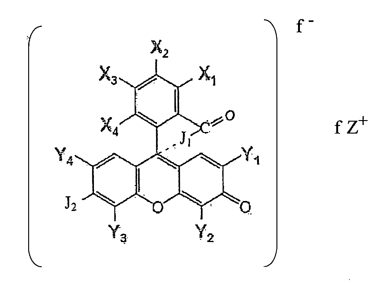
- the fluoresceine derivative is a fluoresceine salt, wherein X 1 , X 2 , X 3 , X 4 and Y 1 , Y 2 , Y 3 , Y 4 are H and the dashed line represents no bond wherein both J 1 and J 2 are O- and 2 Z + are any one of the above-defined organic cations.
- the fluoresceine derivative is an eosine Y salt, wherein X 1 , X 2 , X 3 , X 4 are H, Y 1 , Y 2 , Y 3 , Y 4 are Br, and the dashed line represents no bond, wherein both J 1 and J 2 are O - and 2 Z + are any one of the above-defined organic cations.
- the fluoresceine derivative is a phloxine salt, wherein X 1 , X 2 , X 3 , X 4 are Cl, Y 1 , Y 2 , Y 3 , Y 4 are Br and the dashed line represents no bond, wherein both J 1 and J 2 are O- and 2 Z + are any one of the above-defined organic cations.
- the fluoresceine derivative is Bengale Rose salt, wherein X 1 , X 2 , X 3 , X 4 are Cl, Y 1 , Y 2 , Y 3 , Y 4 are I, and the dashed line represents no bond, wherein both J 1 and J 2 are O - and 2 Z + are any one of the above-defined organic cations.
- the above defined fluoresceine derivatives are known and are generally produced by means of a salification step between an alkali or earth alkali salt of fluoresceine or a derivative thereof with a halide of an organic cation (Z + ).
- the fluoresceine wherein X 1 , X 2 , X 3 , X 4 and Y 1 , Y 2 , Y 3 , Y 4 are H, reacts in its alkali salt form with triethylammonium hydrochloride, for obtaining fluoresceine bis-triethylammonium.
- eosine Y wherein X 1 , X 2 , X 3 , X 4 is H, Y 1 , Y 2 , Y 3 , Y 4 are Br, reacts in its alkali salt form with triethylammonium hydrochloride for obtaining eosine Y bis-triethylammonium.
- phloxine wherein X 1 , X 2 , X 3 , X 4 are Cl, and Y 1 , Y 2 , Y 3 , Y 4 are Br, reacts in its alkali salt form with triethylammonium hydrochloride for obtaining phloxine bis-triethylammonium.
- the present invention also relates to a memory switch comprising a film made of one of the above-defined fluoresceine derivatives.
- the film is made of the above-defined fluoresceine salt wherein X 1 , X 2 , X 3 , X 4 and Y 1 , Y 2 , Y 3 , Y 4 are H, and both 2 Z + are triethylammonium .
- the film is made of the above-defined eosine Y salt wherein X 1 , X 2 , X 3 , X 4 are H, Y 1 , Y 2 , Y 3 , Y 4 are Br, and and both 2 Z + are triethylammonium.
- the film is made of the above-defined phloxine salt wherein X 1 , X 2 , X 3 , X 4 are Cl, Y 1 , Y 2 , Y 3 , Y 4 are Br and both 2 Z + are triethylammonium.
- the film is made of the above-defined Bengale Rose salt, wherein X 1 , X 2 , X 3 , X 4 are Cl, Y 1 , Y 2 , Y 3 , Y 4 are I, and both 2 Z + are triethylammonium.
- the memory switch comprises two metal electrodes between which the film is sandwiched to form a laminate structure.
- the laminate structure comprises a substrate, and either the first electrode or the second electrode is stacked in contact with the top of the substrate.
- the present invention further relates to a memory device comprising the above-defined memory switch.
- the present invention further relates to a method for producing a memory switch comprising two electrodes, wherein the method comprises the step of coating one of the electrodes with a film made of one of the above-defined electrically bistable fluoresceine derivatives.
- the coating step is obtained by means of a spinning step, wherein the fluoresceine derivative is spinned on the surface of electrode, preferably a bottom electrode, to form the film.
- the coating step is performed by means of vacuum deposition of the fluoresceine derivate.
- Disodium Fluorosceine (Fl) (0.40 gr, 1.06 mmoli) and triethylammonium chloride (TEA) (0.3 gr, 2.2 mmoli) suspended in dichloromethane were stirred at room temperature in darkness for 3 h.
- the suspension was filtered by PTFE filter (0.2 ⁇ m) and the filtrate was dried and fully characterized.
- Fluorosceine bis-triethylammonium salt is thus obtained.
- the measured melting point (BÜCHI B-545 instrument) of Fl-TEA is 100-103°C.
- Disodium Eosyne Y (Ey) (0.42 gr) and triethylammonium chloride (TEA) (0.2 gr) suspended in dichloromethane were stirred at room temperature in darkness for 3 h.
- the suspension was filtered by PTFE filter (0.2 ⁇ m) and the filtrate was dried and fully characterized.
- the measured melting point (BÜCHI B-545 instrument) of Ey-TEA is 125-130°C.
- Disodium Phloxine-B (PH) (0.32 gr, 3.8 x 10 -4 moli) and triethylammonium chloride (TEA) (0.2 gr, 1.5 x 10 -3 moli) suspended in dichloromethane were stirred at room temperature in darkness for 3 h.
- the suspension was filtered by PTFE filter (0.2 ⁇ m) and the filtrate was dried and fully characterized.
- Phloxine bis-triethylammonium salt is thus obtained.
- the measured melting point (BÜCHI B-545 instrument) of PH-TEA is 145-150°C.
- Disodium Rose Bengale (BR) (0.32 gr, 3.8 x 10 -4 moli) and triethylammonium chloride (TEA) (0.2 gr, 1.5 x 10 -3 moli) suspended in dichloromethane were stirred at room temperature in darkness for 3 h. The suspension was filtered by PTFE filter (0.2 ⁇ m) and the filtrate was dried and fully characterized.
- BR Disodium Rose Bengale
- TEA triethylammonium chloride
- the measured melting point (BÜCHI B-545 instrument) of BR-TEA is 185°C.
- the organic bistable memory switch 1 comprises a organic thin film 4 formed of one of the above-mentioned fluoresceine derivatives having a organic cation as countercation.
- the organic film 4 is made of one of the salts, which have been synthesized according to the above processes:
- the memory switch 1 further comprises electric signal impressing means (not illustrated in figure 2) for impressing an electric signal between the first electrode 3 and the second electrode 5.
- the memory switch 1 has a laminate structure in which a first electrode 3, the organic thin film 4, and a second electrode 5 are stacked in that order on a substrate 2. More specifically, the first electrode 3, the organic thin film 4, and the second electrode 5 are stacked on the substrate 2 in that order.
- the main function of the substrate 2 is that of supporting the electrodes 3 and 5, and the film 4 provided thereon.
- the substrate 2 is formed of an inorganic base material such as glass, silicon, or quartz or the following organic base material.
- the manoeuvrability of the organic bistable memory switch is improved due to the rigidity imparted by the substrate 2 to the organic bistable device.
- the provision of the substrate facilitates the arrangement of a large number of the elements on the substrate to form a memory device or the like.
- the substrate 2 is formed of an organic base material.
- Organic base materials usable herein include polyamides, polyacetals, polybutylene terephthalate, polyethylene terephthalate, polyethylene naphthalate, syndiotactic polystyrene, polyphenylene sulfide, polyetherether ketone, liquid crystal polymers, fluororesins, polyether nitrile, polycarbonate, modified polyphenylene ether, polycyclohexene, polynorbornene resins, polysulfone, polyether sulfone, polyarylate, polyamideimide, polyetherimide, and thermoplastic polyimides.
- the organic base material is not limited to these materials, and conventional plastics may also be used.
- the use of a thin flexible film having a thickness of about 5 to 300 [mu]m can provide a flexible organic bistable device.
- the first electrode 3 is preferably formed of, for example, a metallic thin film, a relatively high electrically conductive organic thin film, or a thin film of electrically conductive perovskite oxide from the viewpoint of providing proper bonding to the organic thin film 4 as a bistable layer.
- the metallic thin film may be formed of, for example, a highly electrically conductive metal such as Al (aluminum), Pt (platinum), Au (gold), Ag (silver), Fe (iron), Ni (nickel), Cr (chromium), Cu (copper), Ti (titanium), Hf (hafnium), Zn (zinc), Zr (zirconium), Mo (molybdenum), or Ta (tantalum).
- the highly electrically conductive organic thin film may be formed of, for example, PEDOT (3,4-polyethylenedioxythiophenylene/polystyrene sulfate), or properly doped polyaniline, polyacethylene, fullerene, carbon nanotube or carbon nanowire.
- PEDOT polyethylenedioxythiophenylene/polystyrene sulfate
- the electrode may also be formed of a thin film of electrically conductive perovskite oxide.
- Suitable electrically conductive perovskite oxides include IrOx, MnOx, NiOx, CuOx, or RuOx or properly doped product of the above oxides.
- the thickness of the first electrode 3 is preferably about 0.5 nm to 5 [mu]m although the thickness varies depending upon the electrical conductivity of the material.
- the second electrode 5 is formed of a metallic thin film, a relatively high electrically conductive organic thin film, a thin film of an electrically conductive perovskite oxide or the like.
- the thickness of the second electrode 5 may be the same as that of the first electrode 3.
- the memory switch according to the invention is obtained according to the following method.
- the organic thin film 4 is deposited on the first electrode 3, which is the bottom electrode.
- the coating step is performed by means of a spin technique. It consists of preparing a solution of the above fluoresceine salt having a organic countercation in a suitable solvent, as for example methanol, or dichloromethane, to obtain a fluoresceine solution of about 0.1M concentration.
- a suitable solvent as for example methanol, or dichloromethane
- the electrode 3 is introduced in a spin apparatus and placed on a suitable rotating substrate.
- the solution is deposited on the electrode 3, and this latter is rotated at 3000-5000 rpm for 90 sec until the complete evaporation of the solvent.
- An example of a suitable spin apparatus is the Spin coating system Model 6712D from Speciality Coating System provided by Cookson Electronics Company.
- the coating step is performed by means of a gas phase technique, such as a vacuum deposition step.
- the fluoresceine derivative is deposited on the electrode 3, for example by means of a Evaporator System which is provided by Elettro Rava S.p.A. Torino.
- This system comprises a deposition chamber having a source made of the target material to be deposited, i.e. the fluoresceine derivative.
- the chamber is kept under Vacuum (10-8 Torr) and the source is heated at a temperature of 75°C.
- the thickness of the organic thin film 4 is suitably 5 to 1000 nm.
- the organic bistable memory switch thus obtained is suitable for use in a memory device.
- the organic bistable memory switch when used as a memory, whether the organic bistable memory switch 1 is in ON state or in OFF state can be judged by applying a positive or negative pulse voltage to the organic bistable element for a very short period of time to bring the state to writing (ON state) or erasing (OFF state) and then applying a constant voltage, which is a voltage smaller than the absolute value of the pulse voltage for writing or erasing, for a very short period of time.
- the characteristics of the memory switch can be examined by applying a positive or negative voltage across the first electrode 3 and the second electrode 5 to measure current which flows across both the electrodes, or allowing a positive or negative current to flow across both the electrodes to measure voltage across both the electrodes 3, 5.
- the organic bistable element according to the present invention is usable, by utilizing its characteristics, for an organic bistable memory device, which can electrically write, read, and erase information, and for other applications.
- array of memory switches according to the present invention can be arranged in a cross-bar architecture where each memory switch according to the present invention can be combined with either a diode sandwiched below the memory switch, to prevent possible malfunction such as cross-talk, or a transistor (MOSFET, TFT) sandwiched below the memory switch to allow fast access times.
- each memory switch according to the present invention can be combined with either a diode sandwiched below the memory switch, to prevent possible malfunction such as cross-talk, or a transistor (MOSFET, TFT) sandwiched below the memory switch to allow fast access times.
- MOSFET MOSFET
- An organic bistable memory switch shown in FIG. 2 was prepared according to the following procedure.
- ITO covered glasses substrates (1 cm x 2 cm) have been first sonicated for 300 s in a 2-H propanol bath and then dried in an oven at 80°C for 30 min.
- Methanol solutions of BR-TEA 0.1 M have been deposed by spin coating on such substrates (bottom electrode) by using a Spin coating system Model 6712D from Speciality Coating System (Cookson Electronics Company) with several rotation rates (3000-5000 rpm) for 90 sec.
- Figure 3 shows the correlation between the films thickness obtained and the spin rotation rates.
- the gold top electrodes (60-80 nm thick) have been deposed on the organic films by means of Emitech K650X Sputtering Coater operating under argon atmosphere with 20-75 mA for 4 minutes.
- a shadow-mask has been employed obtaining bistable memory switch of size 1.5 x 1.0 mm.
- FIG. 4a and 4b reports the section analysis of BR-TEA films, deposed by using spin rate of 4000 rpm for 90 sec, before (fig. 4a) and after (fig. 4b) the annealing processes.
- the AFM measurements show that the annealing treatment provokes an increase of flattening of the films. Indeed, the related RMS (Root Mean Square) values decrease from 2.5 for the not annealed films to 1.0 nm for the annealed ones.
- Fig. 5 reports the SEM section view of the above reported not annealed BR-TEA films deposed on the silicon substrate. A film thickness of 420 nm is observed.
- Fig. 6 and Fig. 7 shows the I-V characteristic of the BR-TEA based memory switch. A bistable characteristic has been observed with a ON/OFF windows up to 3 order of magnitude, as reported in the enlarged view on the right of Fig. 7.
- the required programming voltages are in the range 1-2 V (negative to program (Set) and positive to erase (Reset)).
- Set negative to program
- Reset positive to erase
- FIG. 8 shows an example of cycle: after the initial characterization, different set pulses and reset pulses have been applied, reading the status after each step. The reading characteristics, performed at low voltage, are perfectly superimposed to the initial characteristic, either low resistance or high resistance, thus proving the intrinsic good switching / cycling behaviour of these devices.
- FIG. 9 A general view of the retention characteristics is presented in Fig. 9. 5s sampling time has been chosen in order to check any variation in the device resistance; -100 mV reading voltage is supposed to be much lower than the set / reset voltage, so that the measurement itself should not disturb the device. From Fig 9, in the measured time window, the set state (low resistance) appears to be stable as the reset state (high resistance).
- An organic bistable memory switch was prepared in the same manner as bistable memory switch 1, except that Bengal Rose disodium salt (BR-Na) was used as the material for the organic thin film. In this case, to improve the films homogeneity the samples have been annealed at 150 °C for 12 h under vacuum.
- Bengal Rose disodium salt BR-Na
- FIG. 10a and 10b report the section analysis of BR-TEA films before (Fig. 10a) and after (Fig. 10b) the annealing process. Also in this case, AFM measurements show that the annealing treatment provokes an increase of the flattening of the films. Indeed, the related RMS values decrease from 0.61 for the not annealed films to 0.5 nm for the annealed ones.
- Fig. 11 depicts the IV curve obtained on such a memory switch by using the same experimental set up of the bistable memory switch 1.
- An organic device shown in FIG. 2 was prepared according to the procedure described in the bistable memory switch 1 except that Fl-TEA was used as the material for the organic film. Some samples have been annealed at 80°C for 8 h under vacuum, some samples have been annealed at 50°C for 8 h under vacuum and some samples has been used without any annealing process.
- bistable memory switch 1 room temperature, in air, by using Agilent 4155C semiconductor parameter analyzer, used in sweep mode to measure the device characteristics and sampling mode to measure the device resistance and the device retention; and Hp81110A pulse generator used to set / reset the status
- the measurements show both bistable IV characteristics and retention characteristics.
- Fig. 12 reports the measurements on not annealed FL-TEA memory switches (solid lines) showing a good cycling behaviour.
- the resistance ratio between SET state and RESET state is something bigger than two. This value is stable.
- the memory window (dotted lines) appears to be similar as in the first measurements, even though a general reduction in current is observed, maybe due to some parasitic resistance.
- the measurements performed on F1-TEA memory switches annealed at 50 C show a much smaller memory window (the factor is much smaller than 2) ; the measurements performed after the retention test (dotted lines) show a reduced memory window, due mainly to the decreased set state current, while the reset state is constant. After some switching, the memory window doesn't seem to be influenced.
- An organic bistable memory switch was prepared in the same manner as in the bistable memory switch 2 except that Fluoresceine disodium salt (Fl-Na) was used as the material for the organic thin film. In this case, to improve the films homogeneity the samples have been annealed at 150 °C for 12 h under vacuum.
- Fluoresceine disodium salt Fl-Na
- An organic device shown in FIG. 2 was prepared according to the procedure described in the bistable memory switch 2 except that Ey-TEA was used as the material for the organic thin film.
- bistable memory switch 2 The electrical measurements performed, by using the same experimental set up reported in bistable memory switch 2 show both bistable IV characteristics and retention characteristics similar to those of bistable memory switch 2.
- An organic bistable memory switch was prepared in the same manner as in the bistable memory switch 3 except that Eosyne Y disodium salt (Ey-Na) was used as the material for the organic thin film. To improve the films homogeneity the samples have been annealed at 150 °C for 12 h under vacuum.
- Eosyne Y disodium salt Ey-Na
- An organic device shown in FIG. 2 was prepared according to the procedure described in the the bistable memory switch 2 except that PH-TEA was used as the material for the organic thin film.
- bistable memory switch 2 The electrical measurements performed, by using the same experimental set up reported in bistable memory switch 2 show both bistable IV characteristics and retention characteristics similar to those of bistable memory switch 2
- An organic bistable memory switch was prepared in the same manner as in the bistable memory switch 4 except that Phloxine disodium salt (PH-Na) was used as the material for the organic thin film. To improve the films homogeneity the samples have been annealed at 150 °C for 12 h under vacuum.
- Phloxine disodium salt PH-Na
- the main advantage of the present invention lies in that, thanks to the organic electrically bistable materials based on fluoresceine derivatives having organic cations as countercation, it is ensured low cations mobility, avoiding the presence of ionic currents that are responsible of electrical drawbacks such as transient bistable behaviours, and decreasing of ON/OFF ratios, etc, etc.
- the low ionic current offers the benefit to obtain memory switch, which are suitable for electronic applications, especially for memory devices:
- fluoresceine derivatives having organic cations as countercation are low cost and easy to process avoiding an increase in production process steps.
- a further advantage is that these materials are compatible to electrode materials given that they do not produce any phenomena of electrode poisoning such as migration into electrode etc etc;
- these materials operates at low drive voltage.
- organic film of the present invention is formed of a single component, namely the fluoresceine derivative.
- the laminate structure is easy to be handled.
- the method according to the invention has the advantage of enabling to obtain a film of fluoresceine salt having a thickness of the film, generally on the order of 5 to 1000 nm.
- the control of the thickness is mainly connected to spin coating step or to the vacuum evaporation step on bottom electrode to form the film.
- the magnitude of the applied bias is low (
- switching back to the high impedance state is achieved by introducing a pulse of polarity opposite that of the previously applied electric field.
- the present invention further has the advantage of providing reliable and reproducible switching in a memory mode.
Abstract
for the production of a electronic device, in particular a memory switch.
Description
- The present invention relates, in its more general aspect, to compounds having the property of being electrically bistable, namely the property of exhibiting voltage-induced conductance switching.
- In particular the present invention relates to Organic Electrically bistable (OEB), and more in particular electrically bistable fluoresceine derivatives.
- The present invention further relates to the use of electrically bistable fluoresceine derivatives for producing electronics components, and in particular memory switches for high density memories applications.
- The present invention also relates to a method for producing switch memories for the production of memory devices.
- Organic Materials showing electrically bistable behaviour are very attractive for the developing of low cost, high density non volatile memory devices.
- Organic Electrically Bistable Materials (OEBMs) can be defined as materials able to have a stable and reversible form upon either charge injection or charge extraction processes.
- More exactly, in these materials when upon electrical stimuli the so-called threshold voltage Vth is reached, the resistivity switches from a low (high) to a high (low) value.
- Thus, this phenomenon allows the material to exhibit two states of different conductivities at the same applied voltage.
- Figure 1 clearly shows one of the typical switching characteristics of organic electrically bistable materials based upon voltage variations.
- The above property makes these materials appealing candidates for use in non-volatile memory applications. Indeed, in comparison to inorganic materials, organic materials offer advantages to allow the tuning of their properties by appropriate syntheses, to be low cost materials and also easy to process materials.
- By examining the prior art on OEBMs, these materials can be grouped in the following main classes: Charge Transfer complexes, Organic Composite systems developed by UCLA University, Simple Organic Molecules, Polymers and Disodium salts of fluoresceine-based dyes, DDQ (2,3-dichloro-5-6-dicyano-1,4-benzoquinone) and TAPA ((+)-2-(2,4,5,7-tetranitro-9-fluorenylideneaminooxy)propionic acid).
- Charge Transfer (CT) Complexes are composed by a D-A system featured by:
- D = metals with low ionization potential such as Cu, Ag, etc. or organic molecules such as e.g. tetrathiafulvalene (TTF)
- A = organic molecules such as e.g. tetracyanoquinodimethane (TQCN), toluylene dicarbamidonitrite (TDCN) etc...
- The use of CT complexes for producing switching device is known for example from the following six patents:
US N° 4,371,883 ;US N° 4, 507,662 ;US N° 4, 574, 366 ;US 4, 652, 894 ;US 4, 731, 756 ; andJP 2001 345431 - Moreover, Cu:TCNQ CT complex has been extensively studied during the last twenty years by Potember et al. [ R.S. Potember et al., Chem. Scr. 17, 219, 1981; Appl. Phys. Lett. 34, 405, 1982; 7 R. S. Potember, T. O. Poehler, A. Rappa, D. O. Cowan, and A. N. Bloch, Synth. Met. 4, 371, 1982. R.S. Potember et al., APL Techn.Dig. 1986, 7, 129; Appl. Phys. Lett. 1995, 67, 2241 and refs therein] and interesting results as materials for high-density memories devices have been found. Basically, these molecules show good stability and fast switching behaviour at room temperature with ease processability (evaporation).
- Nevertheless, these materials present some unsolved technological issues that block their employment in memory devices. Firstly, the electrical behaviour of these materials has generally been found to be unstable, not reproducible and are strictly dependent on both structures and uniformity of films.
- Several methods have been proposed to obtain a precise control of CT film structures [T.Oyamada et al., Appl.Phys.Lett., 2003, 83, 1253 and ref.s therein]. Secondly, the migration of Cu in the electrode materials has been also found with consequent contamination device problems.
- Similar behaviour to Cu:TCNQ has been also demonstrated for the compounds Ag:TCNQ [R.S. Potember et al., APL Techn.Dig. 1986, 7, 129; Appl.Phys.Lett. 1995, 67, 2241 and refs therein], Li:TCNQ [A.J.Gong and Y.Osada, Appl.Phys.Lett., 1992, 61, 2787], Ru:TCNQ [N.Watanabe et al., Phys. Rev.B, 1991, 44, 111]
- Going on to CT complexes review, Xu et al. reports on electrically bistable behaviour of all-organic D-A complexes composed by Melanine cyanurate (MC) +TCNQ and bis[2-butene-2,3-dithiolato(2-)-s.s']-Ni (BBDN) TCNQ, respectively [W.Xu et al., Appl.Phys.Lett., 1995, 67, 2241]. The use of MC and BBDN instead of Cu offer the advantages to avoid the surface Cu migration. The electrical tests showed transition time from high to low resistance < 100 ns, but unfortunately, no switching reversibility suggesting a WORM (Write Once Read-Only memory) applications.
- TTF-CA (a charge transfer complex of tetrathiafulvalene and tetrachloro-p-benzoquinone) have been also studied for use as electrically bistable compound for memories applications (see, for example,
Japanese Patent Laid-Open No. 345431/2001 pages - The molecular structure of the complex has not been revealed. Electrical experiments performed on the devices based on these materials have shown resistance ratio between the high and low conductivity states higher than 100.
- The memory cells exhibited non-volatile data retention of more than 8 months. Moreover, the material, that shows a temperature stability of higher than 250°C, survived several thousand write/erase cycles under ambient conditions without degradation.
- With regard to Organic Composite systems developed by UCLA University, the UCLA compounds are known from the following patent applications
WO/0237500 US 2004/027849 . - Moreover it is known that, UCLA researchers invented a novel organic electrical bistable device (OBD) comprising of a thin metal layer embedded within the organic material, as the active medium [L.Ma et al., Appl.Phys.Lett., 2002, 80, 2997; L.Ma et al., Appl.Phys.Lett., 2003, 82, 1419]. The devices are non-volatile, featured by low transition time and precisely controlled by the application of a positive voltage pulse (to write) or a negative voltage pulse (to erase).
- Disadvantages of such an approach are the presence of complicated structures that involve the necessity to increase the production process steps, and the scalability. Indeed, the scalability perspective for the composite developed by UCLA researchers is much less exciting respect to that related to organic material with single component that can be, in principle, scaled down till single molecule.
- With regard to Simple Organic Molecules, their use is known from the following patents:
CN N° 1,239,329 ;CN N° 1,344,719 ,CN N° 1,333,571 ,CN N° 1,352,470 andCN N° 1,363,936 . - Moreover there are few examples reported in the literature of this class of materials [.G.Li et al.,Appl.Phys.Lett., 2000, 76, 2532; Z.Y.Hua et al., Appl.Surface SCIENCE, 2001, 169-170, 447].
- The first paper [.J.G.Li et al.,Appl.Phys.Lett., 2000, 76, 2532] concerns a device based on 1,1-dicyano-2,2-(4-dimethylaminophenyl) ethylene (DDME). High-quality DDME thin films were grown by a modified vacuum deposition [Z.Q.Xue et al., Thin Solid Film, 1996, 288, 296] and tested in a sandwiched device Au/DDME/Au (cell area 2.25 mm2), fabricated on a Si substrate by usual vacuum deposition. The conductive state was stable at ambient atmosphere. Unfortunately, the switched regions resume the high resistance state when heated to 60 °C in vacuum for about 1 h, accompanied with the color return to brick-red. No reliability data are reported.
- In the second paper [Z.Y.Hua et al., Appl.Surface SCIENCE, 2001, 169-170, 447] the molecular structures of 4-(2-pyridilazo)resorcinol, 1-(2-pyridilazo)2-naphthol, glyoxal-bis-(2hydroxyanil) have been investigated. The resistivity of all these films can be transformed to 6-7 orders of magnitude (from ca. 1010 to 103-104 Ω cm) and, once if the films are in low resistivity state they cannot return to high resistivity state the applied voltage is switched off. The threshold voltage across these organic films with a thickness of 60 nm is 4±6 V and the transition time is 5±10 ns. No reliability data are reported.
- With regard the use of Polymers, D. Ma et al. report results on the electrical characteristics of switching devices constructed using a poly(methacrylate) derivative with pendant anthracene chromophores, poly(methylmethacrylate-co-9-anthracenyl-methylmethacrylate) (10:1) (MDCPAC) [D. Ma et al., Advanced Materials, 2000, 12, 1063]. It has been observed that the Au/MDCPAC/Al device has a switching time from the OFF state to the ON state that is shorter than 0.5 ms and can switch several thousand times. No reliability data are reported.
- Amongst the above-mentioned classes of compounds, disodium salts of fluoresceine-based dyes, as for example (Bengal Rose, Eosyn Y, Fluoresceine disodiumsalt), DDQ (2,3-dichloro-5-6-dicyano-1,4-benzoquinone) and TAPA ((+)-2-(2,4,5,7-tetranitro-9-fluorenylideneaminooxy)propionic acid), are a very recent discover [A.Bandhopadhyay and A.J.Paj, Apl.Phys.Lett., 2003, 82, 1215-1217; A.Bandhopadhyay and A.J.Paj, J.Phys.Chem.B, 2003, 107, 2531-2536; Bandhopadhyay and A.J.Paj, Apl.Phys.Lett., 2003, 82, 1215-1217].
- Devices based on these molecules show electrical bistability with good retention time and cycles.
- Correlation between switching devices based on different fluoresceine derivatives and interesting switching data storage properties is given in the Table here below.
Molecule ON/OFF Ratio Retention Cycles Disodium Bengale Rose salt 105 Tested for h >106 Disodium Eosin Y salt 9800 Tested for h >106 Disodium Fluorescein salt 4 Tested for h >106 DDQ 104 Tested for h >106 TAPA 104 10 h Not rewritable - For this reasons these materials represent an interesting technological compounds for electronics applications.
- Moreover, these disodium salts of fluoresceine-based dyes (Bengale Rose, Eosyn Y, Fluorescein), are low cost, easy to process and operating at low drive voltage, and therefore particularly suitable to be employed in memory devices.
- Nevertheless, disodium salts of fluoresceine-based dyes have however some still unsolved drawbacks.
- The main drawback lies in that when electrical stimuli are applied, disodium salts of fluoresceine-based dyes present ionic currents. From electrical point of view, this is a very negative effect given that causes various drawbacks such as transient bistable behaviours, decreasing of ON/OFF ratios, and films damage.
- Recently, Anirban Bandyopadhyay et al. proposed to produce supramolecular structures of a fluoresceine derivate, namely the Rose Bengal, via layer by layer electrostatic self-assembly (ESA), see A.Bandhopadhyay and A.J.Paj Advanced Materials 2003, 15. No 22, November 17,1949-1952. ESA films of Rose Bengal in a conducting polymer matrix have been obtained, which are used as part of integrated circuit. In particular, three water-soluble polymers as cation (poly(allylamine hydrochloride), poly(diallyldimethylammonium chloride) and poly(p-xylene tetrahydrothiophenium chloride)) and Rose Bengal as anion have been used.
- However, this solution is not free of inconveniences. For example, the use of polymers as cationic layer provides low ON/OFF ratios and unsatisfactory performances of the integrated circuit.
- In view of the above-outlined drawback of the state of the art, the technical problem underlying the present invention is that of providing electrically bistable fluoresceine derivatives, avoiding the presence of ionic currents that are responsible of electrical drawbacks such as transient bistable behaviours and decreasing of ON/OFF ratios.
- Such a technical problem is solved, according to the invention, by the use of a fluoresceine derivative having the following formula:

wherein - X1, X2, X3, X4 and Y1, Y2, Y3, Y4 are independently H, an electron withdrawing group, or an alkyl, aryl, aralkyl, alkenyl, or alkynyl group, or a heterocyclic group;
- the dashed line represents a covalent bond or no bond;
- J1, is
O (oxygen), when the dashed line represents a covalent bond, and
a O-K group or O- , when the dashed line represents no bond; and - J2 is independently an O-K group or O- ;
- wherein K is independently H, an alkyl, aryl, aralkyl, alkenyl, or alkynyl group, a trialkyl-silyl group, a benzensulfonyl group, or a heterocyclic group;
- The electron withdrawing group is preferably selected from F, Cl, Br, I, CN, NO2, COR, CHO, COOH, COOR, CF3, COCl, NH3 +, NR3 +, RCONR,; NO2, SO2R, SCN, CCl3, SO3H or a thio-amidic group having the following formula: RCSNR.
- Preferably, R is an alkyl, aryl, aralkyl, alkenyl, or alkynyl group or an heterocyclic group.
- More preferably R is an aliphatic chain. More preferably R is a C1-C30 alkyl group.
- The term heterocyclic group means a non-aromatic or aromatic monocyclic or polycyclic ring comprising carbon and hydrogen atoms and at least one heteroatom, preferably, 1 to 4 heteroatoms selected from nitrogen, oxygen, and sulfur.
- According to a preferred embodiment, the heterocyclic group is a piperidine or a piperazine.
- Advantageously, according to the invention, a plurality of suitable organic cations can be used which ensure low cations mobility, avoiding the presence of ionic currents that are responsible of electrical drawbacks such as transient bistable behaviours, and decreasing of ON/OFF ratios.
- For example, the organic cation is an alkyl ammonium cation, which is selected from the group of tetra-alkyl-ammonium having formula: (R1)4 N+; tri-alkyl-ammonium having formula: (R1)3NH+, di-alkyl-ammonium having formula: (R1)2NH2 +; alkyl-ammonium having formula: R1NH3 +, wherein R1 is an alkyl group, preferably with 1 to 30 carbon atoms, such as a methyl group, ethyl group, n-propyl group and n-butyl.
- According to a further embodiment of the invention, the organic cation is a sulfonate cation having the following formula Ra-SO2 +, wherein Ra is an alkyl group, preferably with 1 to 30 carbon atoms, such as a methyl group, ethyl group, n-propyl group and n-butyl, an aryl, aralkyl, alkenyl, or alkynyl group, or heterocyclic group.
- Alternatively, the organic cation is a pyridinium cation or an alkyl, aryl, aralkyl, alkenyl, or alkynyl pyridinium cation having the following formula:

- Alternatively, the organic cation is a bipyridinium cation or an alkyl, aryl, aralkyl, alkenyl, or alkynyl bipyridinium cation having formula:

- Alternatively, the bipyridinium cation has the following formula:

- Alternatively, the organic cation is a pyrylium cation having the following formula:


- Alternatively, the organic cation is a thiopyrylium cation having the following formula:

- Preferably the thiopyrylium cation has the following formula:

- Alternatively, the organic cation is an alkyl, aryl, aralkyl, alkenyl, or alkynyl phosphonium cation, in particular having the following formula:
(R2)4P+ where R2 is independently H, alkyl, aryl ,aralkyl, alkenyl, or alkynyl group or a heterocyclic group provided that at least three R2 are independently an alkyl, aryl, aralkyl, alkenyl, or alkynyl group or heterocyclic group, and preferably one of the following formulas:

- Alternatively, the organic cation is an alkyl, aryl, aralkyl, alkenyl, or alkynyl sulfonium cation, in particular (R3)3S+ where R3 is independently alkyl, aryl, aralkyl, alkenyl, or alkynyl group or a heterocyclic group and preferably one of the following formulas:


- Alternatively, the organic cation is an alkyl, aryl, aralkyl, alkenyl, or alkynyl iodonium compound having the following formula: (Rb)2I+, wherein Rb is independently alkyl, aryl, aralkyl, alkenyl, or alkynyl group, or an heterocyclic group.
- Preferably the iodonium cation has one of the following formulas:


- Alternatively, the organic cation is a piperidine cation.
- According to a first embodiment of the present invention, the fluoresceine derivative is a fluoresceine salt, wherein X1, X2, X3, X4 and Y1, Y2, Y3, Y4 are H and the dashed line represents no bond wherein both J1 and J2 are O- and 2 Z+ are any one of the above-defined organic cations.
- According to a second embodiment of the present invention the fluoresceine derivative is an eosine Y salt, wherein X1, X2, X3, X4 are H, Y1, Y2, Y3, Y4 are Br, and the dashed line represents no bond, wherein both J1 and J2 are O- and 2 Z+ are any one of the above-defined organic cations.
- According to a third embodiment of the present invention, the fluoresceine derivative is a phloxine salt, wherein X1, X2, X3, X4 are Cl, Y1, Y2, Y3, Y4 are Br and the dashed line represents no bond, wherein both J1 and J2 are O- and 2 Z+ are any one of the above-defined organic cations.
- According to a fourth embodiment of the present invention, the fluoresceine derivative is Bengale Rose salt, wherein X1, X2, X3, X4 are Cl, Y1, Y2, Y3, Y4 are I, and the dashed line represents no bond, wherein both J1 and J2 are O- and 2 Z+ are any one of the above-defined organic cations.
- The above defined fluoresceine derivatives are known and are generally produced by means of a salification step between an alkali or earth alkali salt of fluoresceine or a derivative thereof with a halide of an organic cation (Z+).
- For example the fluoresceine, wherein X1, X2, X3, X4 and Y1, Y2, Y3, Y4 are H, reacts in its alkali salt form with triethylammonium hydrochloride, for obtaining fluoresceine bis-triethylammonium.
- According to a further example, eosine Y, wherein X1, X2, X3, X4 is H, Y1, Y2, Y3, Y4 are Br, reacts in its alkali salt form with triethylammonium hydrochloride for obtaining eosine Y bis-triethylammonium.
- According to a further example, phloxine wherein X1, X2, X3, X4 are Cl, and Y1, Y2, Y3, Y4 are Br, reacts in its alkali salt form with triethylammonium hydrochloride for obtaining phloxine bis-triethylammonium.
- The present invention also relates to a memory switch comprising a film made of one of the above-defined fluoresceine derivatives.
- According to a preferred embodiment, the film is made of the above-defined fluoresceine salt wherein X1, X2, X3, X4 and Y1, Y2, Y3, Y4 are H, and both 2 Z+ are triethylammonium .
- According to a further preferred embodiment, the film is made of the above-defined eosine Y salt wherein X1, X2, X3, X4 are H, Y1, Y2, Y3, Y4 are Br, and and both 2 Z+ are triethylammonium.
- According to further preferred embodiment, the film is made of the above-defined phloxine salt wherein X1, X2, X3, X4 are Cl, Y1, Y2, Y3, Y4 are Br and both 2 Z+ are triethylammonium.
- Alternatively, the film is made of the above-defined Bengale Rose salt, wherein X1, X2, X3, X4 are Cl, Y1, Y2, Y3, Y4 are I, and both 2 Z+ are triethylammonium.
- Preferably, the memory switch comprises two metal electrodes between which the film is sandwiched to form a laminate structure.
- In a preferred embodiment of the present invention, the laminate structure comprises a substrate, and either the first electrode or the second electrode is stacked in contact with the top of the substrate.
- The present invention further relates to a memory device comprising the above-defined memory switch.
- The present invention further relates to a method for producing a memory switch comprising two electrodes, wherein the method comprises the step of coating one of the electrodes with a film made of one of the above-defined electrically bistable fluoresceine derivatives.
- Preferably, the coating step is obtained by means of a spinning step, wherein the fluoresceine derivative is spinned on the surface of electrode, preferably a bottom electrode, to form the film.
- Alternatively, the coating step is performed by means of vacuum deposition of the fluoresceine derivate.
- Further characteristics and advantages of the invention will be apparent from the following description of some embodiments thereof given by way of indicative and non limiting examples with reference to the annexed drawings.
- In the drawings:
- FIG. 1 one of the typical switching characteristics of organic electrically bistable materials according to the prior art;
- FIG. 2 is a schematic cross-sectional view of a basic laminate structure of the organic bistable memory switch according to the present invention;
- FIG.3 is curve that reports Bengale Rose-bis triethylammonium (BR-TEA) films thickness υs spin rotation rate;
- FIGG. 4a and 4b are Atomic Force Microscopy (AFM) images showing morphology of BR-TEA films (5x5 micron) before and after the annealing processes respectively;
- FIG.5 illustrates the Scanning Electron Spettroscopy (SEM) section view of BR-TEA films on silicon substrate (4000 rpm, 90 sec.);
- FIG.6 illustrates the double sweep characterization of BR-TEA based memory switches;
- FIG. 7 is an enlarged view of the achieved set and reset states for BR-TEA based memory switches;
- FIG. 8 illustrates the current-voltage (I-V) characteristic showing hysteresis and reading sweeps superimposed on it of BR-TEA based memory switches;
- FIG.9 illustrates a general view of the retention behaviour of the set state (high current) and the reset state (low current) of BR-TEA based memory switches;
- FIGG.10a and 10b illustrate the morphology of Bengale Rose-disodium (BR-Na) films (5x5 micron) before and after the annealing processes respectively;
- FIG.11 illustrates the current-voltage (I-V) characteristic of the BR-Na based memory switch;
- FIG.12 illustrates the current-voltage (I-V) characteristic of the Fluorosceine bis-triethylammonium (Fl-TEA) based memory switch before and after retention test;
- FIG. 13 illustrates the current-voltage (I-V) characteristic of the Fl-TEA based memory switch before and after retention test.
- At first with reference to the following examples it will be described the preparation of electrically bistable fluoresceine derivatives according to the invention.
- In particular, the following fluoresceine derivatives have been prepared:
- fluoresceine salt wherein the organic salt is triethyl-ammonium (TEA);
- eosyne Y salt wherein the organic salt is triethyl-ammonium (TEA);
- phloxine salt wherein the organic salt is triethyl-ammonium (TEA); and
- Bengale Rose salt wherein the organic salt is triethyl-ammonium (TEA).
- The preparation of the above reported salts has been carried out as follows:
- 10 ml of triethylamina (0.072 mol) was dropped, in ice bath, in 9 ml di HCl 12 M (0.109 mol) and stirred for 3 hs (Scheme 1). The solvent was taken off under reduced pressure and the obtained white solid was washed several times with methanol and dichloromethane and dried under vacuum.

- The molecular characterization of TEA was carried out by Mass Spectrometry (MS) and FTIR analyses.
- MS analysis. Mass spectrum of TEA was carried out in methanol solution and the following diagnostic peaks are present: [TEA]+ 101.9 m/z (100%) 102.9 m/z (10%).
- FTIR analysis. Infrared spectrum, obtained on solid state, exhibits the peaks diagnostic of TEA: C-H stretch. 2969 cm-1, CH3 strech. 2931, 2873 cm-1; N-H strech.- 2600 2498 cm-1; C-H bend. 1479, 1390 cm-1; C-N stretch. 1030 cm-1.
- Disodium Fluorosceine (Fl) (0.40 gr, 1.06 mmoli) and triethylammonium chloride (TEA) (0.3 gr, 2.2 mmoli) suspended in dichloromethane were stirred at room temperature in darkness for 3 h.
- The following
scheme 2 clearly illustrates the synthesis process (salification) of fluorosceine bis-triethylammonium salt. - The suspension was filtered by PTFE filter (0.2 µm) and the filtrate was dried and fully characterized.
- Fluorosceine bis-triethylammonium salt is thus obtained.
- The molecular characterization of Fl-TEA was carried out by Mass Spectrometry (MS), Nuclear Magnetic Resonance (NMR) and FTIR Infrared Spectroscopy analyses.
- MS analysis. Mass spectrum of Fl-TEA in methanol solution exhibits the following diagnostic peaks: [F1] - - 165.4 m/z2 e [Fl---TEA+]- 431.3 m/z.
- NMR analysis. 1H-NMR spectrum in CD2Cl2 (200MHz) shows the following diagnostic peaks: δ 1.1 (18H, t, J=7.4 Hz, ethyl CH 3 -CH2-); 2.77 (12H, q,ethyl CH3-CH 2 ); 6.46 (1H d, J=2.2 Hz, xanthene-H), 6.5 (1H d, J=2.0 Hz, xanthene-H), 6.57 (2H d, J=2.2 Hz, xanthene-H), 6.85 (1H s, xanthene-H), 6.89 (1H s, xanthene-H); 7.17 (1H m, Jorto=5.5 Hz, Jmeta=3.0 Hz, benzene-H), 7.58 (2H m, Jorto=5.7 Hz, Jmeta=2.9 Hz, benzene-H); 8.07 (1H m, Jorto=5.8 Hz, Jmeta=2.8 Hz, benzene-H).
- FTIR analysis. Infrared spectrum of F1-TEA carried out in solid state exhibits the following characteristic peaks of triethylammonium: C-H strech. 2987 cm-1; N-H strech.- 2610-2491 cm-1. Furthermore the typical fingerprint of fluoroscein-dyes are present (1627 cm-1, 1561 cm-1, 1450 cm-1, 1318 cm-1, 1222 cm-1, 970 cm-1) that confirms the molecular structure of Fl-TEA.
- The measured melting point (BÜCHI B-545 instrument) of Fl-TEA is 100-103°C.


- Disodium Eosyne Y (Ey) (0.42 gr) and triethylammonium chloride (TEA) (0.2 gr) suspended in dichloromethane were stirred at room temperature in darkness for 3 h. The suspension was filtered by PTFE filter (0.2 µm) and the filtrate was dried and fully characterized.
- Eosyne Y bis-triethylammonium salt is thus obtained.
- The following
scheme 3 clearly illustrates the synthesis process of eosyne Y bis-triethylammonium salt. - The molecular characterization of Ey-TEA was carried out by Mass Spectrometry (MS), Nuclear Magnetic Resonance (NMR) and FTIR Infrared Spectroscopy analyses.
- MS analysis. Mass spectrum (ESI-MS) of Ey-TEA was carried out in methanol solution and show the follows diagnostic peaks: [Ey] - 485.7m/z2, [Ey---TEA+]- 1072.9 m/z.
- NMR analysis. 1H-NMR spectrum in CD2Cl2 (200MHz) exhibits the following diagnostic peaks: δ 1.22 (18H, t, J=7.2 Hz, ethyl CH 3 -CH2-); 2.94 (12H, q,ethyl CH3-CH 2 ); 7.28 (2H s, xanthene-H); 7.14 (1H m, Jorto=6.0 Hz, benzene-H), 7.55 (2H m, benzene-H); 8.14 (1H m, Jorto=6.9 Hz, benzene-H). FTIR analysis. Infrared spectrum of Ey-TEA was carried out in solid state and shows the following characteristic peaks of triethyl ammonium: C-H strech. 2969 cm-1; N-H strech.- 26132-2498 cm-1. Furthermore the typical fingerprint of fluoroscein-dyes are present (1627 C=O 1740 cm-1) that confirms the molecular structure of Ey-TEA.
- The measured melting point (BÜCHI B-545 instrument) of Ey-TEA is 125-130°C.

- Disodium Phloxine-B (PH) (0.32 gr, 3.8 x 10⁻⁴moli) and triethylammonium chloride (TEA) (0.2 gr, 1.5 x 10⁻³moli) suspended in dichloromethane were stirred at room temperature in darkness for 3 h. The suspension was filtered by PTFE filter (0.2 µm) and the filtrate was dried and fully characterized.
- Phloxine bis-triethylammonium salt is thus obtained.
- The following
scheme 4 clearly illustrates the synthesis process of phloxine bis-triethylammonium salt. - The molecular characterization of PH-TEA was carried out by Mass Spectrometry (MS), Nuclear Magnetic Resonance (NMR) and FTIR Infrared Spectroscopy analyses.
- MS analysis. Mass spectrum of PH-TEA in methanol solution shows the following diagnostic peaks: [PH]--391.3 m/z2, [PH---TEA+]- 885.56 m/z.
- NMR analysis. 1H-NMR spectrum in CD2Cl2 (200MHz) exhibits the following diagnostic peaks: δ 1.22 (18H, t, J=7.2 Hz, ethyl CH 3 -CH2-); 2.96 (12H, q, ethyl CH3-CH2); 7.29 (2H s, xanthene-H).
- FTIR analysis. Infrared spectrum of PH-TEA carried out in solids state shows the presence of the following characteristic peaks of triethylammonium: C-H strech. 2982 cm-1; N-H strech.- 2622-2501 cm-1. Furthermore the typical fingerprint of fluoroscein-dyes are present (1627 cm-1, 1561 cm-1, 1450 cm-1, 1318 cm-1, 1222 cm-1, 970 cm-1) that confirms the molecular structure of PH-TEA.
- The measured melting point (BÜCHI B-545 instrument) of PH-TEA is 145-150°C.

- Disodium Rose Bengale (BR) (0.32 gr, 3.8 x 10⁻⁴moli) and triethylammonium chloride (TEA) (0.2 gr, 1.5 x 10⁻³moli) suspended in dichloromethane were stirred at room temperature in darkness for 3 h. The suspension was filtered by PTFE filter (0.2 µm) and the filtrate was dried and fully characterized.
- Bengale Rose bis-triethylammonium salt is thus obtained.
- The following
scheme 5 clearly illustrates the synthesis process of bengale rose bis-triethylammonium salt. - The molecular characterization of BR-TEA was carried out by Mass Spectrometry (MS), Nuclear Magnetic Resonance (NMR) and FTIR Infrared Spectroscopy analyses
- MS analysis. Mass spectrum of BR-TEA in methanol solution shows the following diagnostic peaks: [BR]--971 m/z2, [BR---TEA+]- 1073. m/z.
- NMR analysis. 1H-NMR spectrum in CD2Cl2 (200MHz) exhibits the following diagnostic peaks: δ 1.22 (18H, t, J=7.2 Hz, ethyl CH 3 -CH2-); 2.96 (12H, q, ethyl CH3-CH 2 ); 7.52 (2H s, xanthene-H).
- FTIR analysis. Infrared spectrum of BR-TEA carried out in solids state shows the presence of the following characteristic peaks of triethylammonium: C-H strech. 2982 cm-1; N-H strech.- 2622-2501 cm-1. Furthermore the typical fingerprint of fluoroscein-dyes are present (1627 cm-1, 1561 cm-1, 1450 cm-1, 1318 cm-1, 1222 cm-1, 970 cm-1) that confirms the molecular structure of PH-TEA.
- The measured melting point (BÜCHI B-545 instrument) of BR-TEA is 185°C.

- With reference to figure 2, an organic
bistable memory switch 1 according to the invention is now disclosed. - The organic
bistable memory switch 1 comprises a organicthin film 4 formed of one of the above-mentioned fluoresceine derivatives having a organic cation as countercation. - More in details, in the illustrated solution, the
organic film 4 is made of one of the salts, which have been synthesized according to the above processes: - fluoresceine salt wherein the organic salt is triethyl-ammonium (TEA);
- eosyne Y salt wherein the organic salt is the organic salt is triethyl-ammonium (TEA);
- phloxine salt wherein the organic salt is triethyl-ammonium (TEA); and
- Bengale Rose salt wherein the organic salt is triethyl-ammonium (TEA). The
memory switch 1 further comprises, afirst electrode 3 and asecond electrode 5, between which theorganic film 4 is sandwiched. - The
memory switch 1 further comprises electric signal impressing means (not illustrated in figure 2) for impressing an electric signal between thefirst electrode 3 and thesecond electrode 5. - More in details, the
memory switch 1 according to the present invention has a laminate structure in which afirst electrode 3, the organicthin film 4, and asecond electrode 5 are stacked in that order on asubstrate 2. More specifically, thefirst electrode 3, the organicthin film 4, and thesecond electrode 5 are stacked on thesubstrate 2 in that order. - It is to be noticed that, the main function of the
substrate 2 is that of supporting theelectrodes film 4 provided thereon. - The
substrate 2 is formed of an inorganic base material such as glass, silicon, or quartz or the following organic base material. - It is also to be noted that, thanks to the presence of the
substrate 2, the manoeuvrability of the organic bistable memory switch is improved due to the rigidity imparted by thesubstrate 2 to the organic bistable device. - Further, the provision of the substrate facilitates the arrangement of a large number of the elements on the substrate to form a memory device or the like.
- In addition, according to a further embodiment, the
substrate 2 is formed of an organic base material. - Organic base materials usable herein include polyamides, polyacetals, polybutylene terephthalate, polyethylene terephthalate, polyethylene naphthalate, syndiotactic polystyrene, polyphenylene sulfide, polyetherether ketone, liquid crystal polymers, fluororesins, polyether nitrile, polycarbonate, modified polyphenylene ether, polycyclohexene, polynorbornene resins, polysulfone, polyether sulfone, polyarylate, polyamideimide, polyetherimide, and thermoplastic polyimides. The organic base material, however, is not limited to these materials, and conventional plastics may also be used.
- In particular, when the
substrate 2 is formed of an organic base material, the use of a thin flexible film having a thickness of about 5 to 300 [mu]m can provide a flexible organic bistable device. - The
first electrode 3 is preferably formed of, for example, a metallic thin film, a relatively high electrically conductive organic thin film, or a thin film of electrically conductive perovskite oxide from the viewpoint of providing proper bonding to the organicthin film 4 as a bistable layer. The metallic thin film may be formed of, for example, a highly electrically conductive metal such as Al (aluminum), Pt (platinum), Au (gold), Ag (silver), Fe (iron), Ni (nickel), Cr (chromium), Cu (copper), Ti (titanium), Hf (hafnium), Zn (zinc), Zr (zirconium), Mo (molybdenum), or Ta (tantalum). - The highly electrically conductive organic thin film may be formed of, for example, PEDOT (3,4-polyethylenedioxythiophenylene/polystyrene sulfate), or properly doped polyaniline, polyacethylene, fullerene, carbon nanotube or carbon nanowire.
- The electrode may also be formed of a thin film of electrically conductive perovskite oxide. Suitable electrically conductive perovskite oxides include IrOx, MnOx, NiOx, CuOx, or RuOx or properly doped product of the above oxides. The thickness of the
first electrode 3 is preferably about 0.5 nm to 5 [mu]m although the thickness varies depending upon the electrical conductivity of the material. - As with the
first electrode 3, thesecond electrode 5 is formed of a metallic thin film, a relatively high electrically conductive organic thin film, a thin film of an electrically conductive perovskite oxide or the like. - The thickness of the
second electrode 5 may be the same as that of thefirst electrode 3. - The memory switch according to the invention, is obtained according to the following method.
- In a first step, so called coating step, the organic
thin film 4 is deposited on thefirst electrode 3, which is the bottom electrode. - More in particular, the coating step is performed by means of a spin technique. It consists of preparing a solution of the above fluoresceine salt having a organic countercation in a suitable solvent, as for example methanol, or dichloromethane, to obtain a fluoresceine solution of about 0.1M concentration.
- The
electrode 3 is introduced in a spin apparatus and placed on a suitable rotating substrate. - The solution is deposited on the
electrode 3, and this latter is rotated at 3000-5000 rpm for 90 sec until the complete evaporation of the solvent. - An example of a suitable spin apparatus is the Spin coating system Model 6712D from Speciality Coating System provided by Cookson Electronics Company.
- According to a further embodiment, the coating step is performed by means of a gas phase technique, such as a vacuum deposition step.
- In this case, the fluoresceine derivative is deposited on the
electrode 3, for example by means of a Evaporator System which is provided by Elettro Rava S.p.A. Torino. - This system comprises a deposition chamber having a source made of the target material to be deposited, i.e. the fluoresceine derivative.
- The chamber is kept under Vacuum (10-8 Torr) and the source is heated at a temperature of 75°C.
- Under these conditions a rate deposition of 0.3 A° / sec is obtained
- The thickness of the organic
thin film 4 is suitably 5 to 1000 nm. - The organic bistable memory switch thus obtained is suitable for use in a memory device.
- In particular, when the organic bistable memory switch is used as a memory, whether the organic
bistable memory switch 1 is in ON state or in OFF state can be judged by applying a positive or negative pulse voltage to the organic bistable element for a very short period of time to bring the state to writing (ON state) or erasing (OFF state) and then applying a constant voltage, which is a voltage smaller than the absolute value of the pulse voltage for writing or erasing, for a very short period of time. The characteristics of the memory switch can be examined by applying a positive or negative voltage across thefirst electrode 3 and thesecond electrode 5 to measure current which flows across both the electrodes, or allowing a positive or negative current to flow across both the electrodes to measure voltage across both theelectrodes - As described above, the organic bistable element according to the present invention is usable, by utilizing its characteristics, for an organic bistable memory device, which can electrically write, read, and erase information, and for other applications.
- In this context, array of memory switches according to the present invention can be arranged in a cross-bar architecture where each memory switch according to the present invention can be combined with either a diode sandwiched below the memory switch, to prevent possible malfunction such as cross-talk, or a transistor (MOSFET, TFT) sandwiched below the memory switch to allow fast access times.
- An organic bistable memory switch shown in FIG. 2 was prepared according to the following procedure.
- ITO covered glasses substrates (1 cm x 2 cm) have been first sonicated for 300 s in a 2-H propanol bath and then dried in an oven at 80°C for 30 min. Methanol solutions of BR-TEA 0.1 M have been deposed by spin coating on such substrates (bottom electrode) by using a Spin coating system Model 6712D from Speciality Coating System (Cookson Electronics Company) with several rotation rates (3000-5000 rpm) for 90 sec. Figure 3 shows the correlation between the films thickness obtained and the spin rotation rates.
- To improve the films homogeneity some samples have been annealed at 80 °C for 8 hours under vacuum.
- The gold top electrodes (60-80 nm thick) have been deposed on the organic films by means of Emitech K650X Sputtering Coater operating under argon atmosphere with 20-75 mA for 4 minutes. A shadow-mask has been employed obtaining bistable memory switch of size 1.5 x 1.0 mm.
- The morphology of BR-TEA films has been inspected by AFM. Figure 4a and 4b reports the section analysis of BR-TEA films, deposed by using spin rate of 4000 rpm for 90 sec, before (fig. 4a) and after (fig. 4b) the annealing processes. The AFM measurements show that the annealing treatment provokes an increase of flattening of the films. Indeed, the related RMS (Root Mean Square) values decrease from 2.5 for the not annealed films to 1.0 nm for the annealed ones.
- Fig. 5 reports the SEM section view of the above reported not annealed BR-TEA films deposed on the silicon substrate. A film thickness of 420 nm is observed.
- Electrical characterization has been performed on BR-TEA based memory switch prepared by spinning the organic film at 4000 rpm and annealing it as above described. The experimental condition and set up have been: room temperature, in air, of Agilent 4155C semiconductor parameter analyzer, used in:
- sweep mode to measure the device characteristics;
- sampling mode to measure the device resistance and the device retention;
- Fig. 6 and Fig. 7 shows the I-V characteristic of the BR-TEA based memory switch. A bistable characteristic has been observed with a ON/OFF windows up to 3 order of magnitude, as reported in the enlarged view on the right of Fig. 7.
- For these devices, the required programming voltages are in the range 1-2 V (negative to program (Set) and positive to erase (Reset)). By convention it has been defined the following states in which the memory is set:
- Set status: low resistance
- Reset status: high resistance
- To check the cycling memory behaviour, the following measurements have been performed:
- Memory set (programming, that is transition from high resistance to low resistance), this has been obtained by applying a programming pulse of 1 - 2 V amplitude, 1 ms - 10 ms duration
- Read memory set status: current is measured at low voltage, in order not to disturb the system (either -100 mV or 100 mV);
- Memory reset (from low resistance to high resistance): this has been obtained by applying an erasing pulse of -1 - -2 V amplitude, 1 ms - 10 ms duration
- Read reset status: same measurement as set status
- Cycling behaviour has been also observed on these based memory switches. A reproducible bi-stable characteristic has been measured for tenths of cycles with 1 ms programming / erasing pulses, with ± 1.5 V amplitude. Fig. 8 shows an example of cycle: after the initial characterization, different set pulses and reset pulses have been applied, reading the status after each step. The reading characteristics, performed at low voltage, are perfectly superimposed to the initial characteristic, either low resistance or high resistance, thus proving the intrinsic good switching / cycling behaviour of these devices.
- Memory retention has been measured as follows:
- 1. Memory is set;
- 2. Memory status is read every 5 s at room temperature for 1000 s
- 3. Memory is reset;
- 4. Memory status read every 5 s at room temperature for 1000 s.
- A general view of the retention characteristics is presented in Fig. 9. 5s sampling time has been chosen in order to check any variation in the device resistance; -100 mV reading voltage is supposed to be much lower than the set / reset voltage, so that the measurement itself should not disturb the device. From Fig 9, in the measured time window, the set state (low resistance) appears to be stable as the reset state (high resistance).
- An organic bistable memory switch was prepared in the same manner as
bistable memory switch 1, except that Bengal Rose disodium salt (BR-Na) was used as the material for the organic thin film. In this case, to improve the films homogeneity the samples have been annealed at 150 °C for 12 h under vacuum. - The morphology of BR-Na films has been studied by AFM. Figures 10a and 10b report the section analysis of BR-TEA films before (Fig. 10a) and after (Fig. 10b) the annealing process. Also in this case, AFM measurements show that the annealing treatment provokes an increase of the flattening of the films. Indeed, the related RMS values decrease from 0.61 for the not annealed films to 0.5 nm for the annealed ones.
- For this organic bistable memory switch, no bistable characteristic has been observed but a very little hysteretic effect mainly due to ions movement. Fig. 11 depicts the IV curve obtained on such a memory switch by using the same experimental set up of the
bistable memory switch 1. - An organic device shown in FIG. 2 was prepared according to the procedure described in the
bistable memory switch 1 except that Fl-TEA was used as the material for the organic film. Some samples have been annealed at 80°C for 8 h under vacuum, some samples have been annealed at 50°C for 8 h under vacuum and some samples has been used without any annealing process. - The electrical measurements performed, by using the same experimental set up reported in bistable memory switch 1 (room temperature, in air, by using Agilent 4155C semiconductor parameter analyzer, used in sweep mode to measure the device characteristics and sampling mode to measure the device resistance and the device retention; and Hp81110A pulse generator used to set / reset the status) are:
- 1. transcharacteristics performed between -1.8 V to 1.8 V, with double setting, in order to get any hysteresis if any is present. These characteristics have been performed only on one sample and here not reported, as they can be destructive towards the sample itself. They have been done in order to get the typical set - reset voltages and the typical device current.
- 2. the best set - reset conditions that have been found are:
- a. set voltage: +1.5 V
- b. reset voltage: -1.5 V
- c. set pulse length: 10 ms
- d. reset pulse length: 10 ms
- e. current compliance: 20 mA
- 3. some manual cycling has been performed; after this, short time retention test has been performed at room temperature, that is:
- a. the memory is left in reset state
- b. every second the memory state is read till 1000 seconds
- c. the memory is switched into set state
- d. every second the memory state is read till 1000 seconds
- e. the memory is finally switched again
- The measurements show both bistable IV characteristics and retention characteristics.
- Fig. 12 reports the measurements on not annealed FL-TEA memory switches (solid lines) showing a good cycling behaviour. The resistance ratio between SET state and RESET state is something bigger than two. This value is stable.
- After retention measurements, the memory window (dotted lines) appears to be similar as in the first measurements, even though a general reduction in current is observed, maybe due to some parasitic resistance.
- The measurements performed on F1-TEA memory switches annealed at 50 C (FIG.13) show a much smaller memory window (the factor is much smaller than 2) ; the measurements performed after the retention test (dotted lines) show a reduced memory window, due mainly to the decreased set state current, while the reset state is constant. After some switching, the memory window doesn't seem to be influenced.
- Finally, the measurements performed on Fl-TEA memory switches annealed at 80 C don't show any switching behaviour.
- An organic bistable memory switch was prepared in the same manner as in the
bistable memory switch 2 except that Fluoresceine disodium salt (Fl-Na) was used as the material for the organic thin film. In this case, to improve the films homogeneity the samples have been annealed at 150 °C for 12 h under vacuum. - For this organic bistable memory switch, no bistable characteristic has been observed but a very little hysteretic effect mainly due to Na + ions movement. The IV curve obtained on such a device is qualitatively the same of comparative
bistable memory switch 1 and reported in fig.11. - An organic device shown in FIG. 2 was prepared according to the procedure described in the
bistable memory switch 2 except that Ey-TEA was used as the material for the organic thin film. - The electrical measurements performed, by using the same experimental set up reported in
bistable memory switch 2 show both bistable IV characteristics and retention characteristics similar to those ofbistable memory switch 2. - An organic bistable memory switch was prepared in the same manner as in the
bistable memory switch 3 except that Eosyne Y disodium salt (Ey-Na) was used as the material for the organic thin film. To improve the films homogeneity the samples have been annealed at 150 °C for 12 h under vacuum. - For this organic bistable memory switch, no bistable characteristic has been observed but a very little hysteretic effect mainly due to ions movement. The IV curve obtained on such a device is qualitatively the same of comparative
bistable memory switch 1 and reported in fig.11. - An organic device shown in FIG. 2 was prepared according to the procedure described in the the
bistable memory switch 2 except that PH-TEA was used as the material for the organic thin film. - The electrical measurements performed, by using the same experimental set up reported in
bistable memory switch 2 show both bistable IV characteristics and retention characteristics similar to those ofbistable memory switch 2 - An organic bistable memory switch was prepared in the same manner as in the
bistable memory switch 4 except that Phloxine disodium salt (PH-Na) was used as the material for the organic thin film. To improve the films homogeneity the samples have been annealed at 150 °C for 12 h under vacuum. - For this organic bistable memory switch, no bistable characteristic has been observed but a very little hysteretic effect mainly due to ions movement. The IV curve obtained on such a device is qualitatively the same of comparative
bistable memory switch 1 and reported in fig.11. - The main advantage of the present invention lies in that, thanks to the organic electrically bistable materials based on fluoresceine derivatives having organic cations as countercation, it is ensured low cations mobility, avoiding the presence of ionic currents that are responsible of electrical drawbacks such as transient bistable behaviours, and decreasing of ON/OFF ratios, etc, etc.
- The low ionic current offers the benefit to obtain memory switch, which are suitable for electronic applications, especially for memory devices:
- Moreover, fluoresceine derivatives having organic cations as countercation are low cost and easy to process avoiding an increase in production process steps.
- A further advantage is that these materials are compatible to electrode materials given that they do not produce any phenomena of electrode poisoning such as migration into electrode etc etc;
- Moreover, these materials operates at low drive voltage.
- A further not less important advantage lies in that to organic film of the present invention is formed of a single component, namely the fluoresceine derivative.
- The presence of a single component enables the film to be, in principle, scaled down till "single molecule".
- It represents a good starting point for the production of molecular memory nano-devices.
- It is an advantage of the invention to have laminate structure comprising the first and second electrodes, between which a thin film of the fluoresceine-salt is sandwiched. The laminate structure is easy to be handled.
- In this regard, the method according to the invention has the advantage of enabling to obtain a film of fluoresceine salt having a thickness of the film, generally on the order of 5 to 1000 nm.
- The control of the thickness is mainly connected to spin coating step or to the vacuum evaporation step on bottom electrode to form the film.
- It is a further advantage of the invention to provide switching from a high impedance state to a low impedance state by applying an electric field of any polarity.
- The magnitude of the applied bias is low (| 1-2V|). As a matter of fact thanks to the invention, switching back to the high impedance state is achieved by introducing a pulse of polarity opposite that of the previously applied electric field.
- This enables to provide a device, which acts as an organic, electrochemical storage cell when passing from a low to a high impedance state.
- The present invention further has the advantage of providing reliable and reproducible switching in a memory mode.
- Obviously, a technician of the field, in order to satisfy contingent, specific needs will bring several modifications and variations to the above described method and composite structure, all within the scope of protection of the invention as defined by the following claims.
provided that at least one of J1 and J2 is a O- and then f is 1 or 2,
with the further proviso that the organic cation is different from a cationic polymer.
Claims (41)
- Use of a fluoresceine derivative having the following formula:

wherein- X1, X2, X3, X4 and Y1, Y2, Y3, Y4 are independently H, an electron withdrawing group, or an alkyl, aryl, aralkyl, alkenyl, or alkynyl group, or a heterocyclic group;- the dashed line represents a covalent bond or no bond;- J1, is
O (oxygen), when the dashed line represents a covalent bond, and
a O-K group or O- , when the dashed line represents no bond; and- J2 is independently an O-K group or O- ;- wherein K is independently H, an alkyl, aryl, aralkyl, alkenyl, or alkynyl group, a trialkyl-silyl group, a benzensulfonyl group, or a heterocyclic group,and Z+ is an organic cation,
provided that at least one of J1 and J2 is a O- and then f is 1 or 2,
with the further proviso that the organic cation is different from a cationic polymer. - Use according to claim 1, wherein the organic cation is an alkyl ammonium cation, which is selected from the group of tetra-alkyl-ammonium of formula (R1)4N+; tri-alkyl-ammonium of formula (R1)3NH+, di-alkyl-ammonium having formula: (R1)2NH2 +; alkyl-ammonioum having formula : R1NH3+, wherein R1 is an alkyl group with 1 to 30 carbon atoms, in particular a methyl group, ethyl group, n-propyl group and n-butyl.
- Use according to claim 1, wherein the organic cation is a sulfonate cation having the following formula Ra-SO2 +, wherein Ra is an alkyl group, preferably with 1 to 30 carbon atoms, such as a methyl group, ethyl group, n-propyl group and n-butyl, an aryl, aralkyl, alkenyl, or alkynyl group, or heterocyclic group.
- Use according to claim 1, wherein the organic cation is a bipyridinium cation or an alkyl, aryl, aralkyl alkenyl, or alkynyl bipyridinium cation having formula:

- Use according to claim 1, wherein the organic cation is a bipyridinium cation having the following formula:

- Use according to claim 1, wherein the organic cation is a pyrylium cation having the following formula:

- Use according to claim 6, wherein the pyrylium cation has one of following formulas:


- Use according to claim 1, wherein the organic cation is thio-pyrylium having the following formula:

- Use according to claim 8, wherein the thio-pyrylium has the following formula:

- Use according to claim 1, wherein the organic cation is an alkyl, aryl, aralkyl, alkenyl , or alkynyl phosphonium cation, in particular (R2)4P+ where R2 is independently H, alkyl, aryl, aralkyl, alkenyl , or alkynyl group or a heterocyclic group, provided that at least three R2 are independently an alkyl, aryl, aralkyl group, alkenyl, or alkynyl group, or a heterocyclic group, and preferably one of the following formulas:


- Use according to claim 1, wherein the organic cation is an alkyl, aryl, aralkyl, alkenyl, or alkynyl sulfonium cation, in particular (R3)3S+ where R3 is independently alkyl, aryl, aralkyl, alkenyl, or alkynyl group or a heterocyclic group and one of the following formulas:


- Use according to claim 1, wherein the organic cation is an alkyl, aryl, aralkyl, alkenyl, or alkynyl iodonium compound having the following formula: (Rb)2I+, wherein Rb is independently alkyl, aryl, aralkyl, alkenyl , or alkynyl group, or an heterocyclic group.
- Use of claim 12, wherein the iodonium cation has one of the following formulas:


- Use according to claim 1, wherein the organic cation is a piperidine cation.
- Use according to any of preceding claims, wherein the electron withdrawing group is selected from F, Cl, Br, I, CN, NO2, COR, CHO, COOH, COOR, CF3, COCl, NH3 +, NR3 +, NO2, SO2R, SCN, CCl3, SO3H RCONR, or a thio-amidic group of formula RCSNR.
- Use according to claim 15, wherein R is an alkyl, aryl, aralkyl, alkenyl, or alkynyl group or an heterocyclic group.
- Use according to claim 15, wherein R is an aliphatic chain, in particular a C1-C30 alkyl.
- Use according to claim 1, wherein the organic cation is a pyridinium cation or an alkyl, aryl, aralkyl, alkenyl, or alkynyl pyridinium cation, having the following formula:

- Use according to any one of preceding claims, wherein the fluoresceine derivative is a fluoresceine salt, wherein X1, X2, X3, X4 and Y1, Y2, Y3, Y4 are H and the dashed line represents no bond wherein both J1 and J2 are O-.
- Use according to any one of preceding claims 1 to 18, wherein the fluoresceine derivative is an eosine Y salt, wherein X1, X2, X3, X4 are H, Y1, Y2, Y3, Y4 are Br, and the dashed line represents no bond, wherein both J1 and J2 are O-.
- Use according to any one of preceding claims 1 to 18, wherein the fluoresceine derivative is a phloxine salt, wherein X1, X2, X3, X4 are Cl, Y1, Y2, Y3, Y4 are Br and the dashed line represents no bond, wherein both J1 and J2 are O-.
- Use according to any one of preceding claims 1 to 18, wherein the fluoresceine derivative is Bengale Rose salt, wherein X1, X2, X3, X4 are Cl, Y1, Y2, Y3, Y4 are I, and the dashed line represents no bond, wherein both J1 and J2 are O-.
- Use according to any one of preceding claims 19 to 22, wherein Z+ is triethylammonium
- Memory switch comprising a film made of anyone of the fluoresceine derivatives according to claims 1 to 23.
- Memory switch according to claim 24, wherein the fluoresceine derivative is a fluoresceine salt wherein X1, X2, X3, X4 and Y1, Y2, Y3, Y4 are H, and both 2 Z+ are triethylammonium.
- Memory switch according to claim 24, wherein the fluoresceine derivative is an eosine Y salt wherein X1, X2, X3, X4 are H, Y1, Y2, Y3, Y4 are Br, and and both 2 Z+ are triethylammonium.
- Memory switch according to claim 24, wherein the fluoresceine derivative is a phloxine salt wherein X1, X2, X3, X4 are Cl, Y1, Y2, Y3, Y4 are Br and both 2 Z+ are triethylammonium.
- Memory switch according to claim 24, wherein the fluoresceine derivative is a Bengale Rose salt, wherein X1, X2, X3, X4 are Cl, Y1, Y2, Y3, Y4 are I, and both 2 Z+ are triethylammonium.
- Memory switch according to any one of preceding claims 24 to 28, which further comprises two metal electrodes (3, 5) between which the film (4) is sandwiched to form a laminate structure.
- Memory switch according to any one of preceding claims 24 to 29, wherein the film (4) has a thickness of about 5 to 1000 nm.
- Memory switch according to any one of preceding claims 24 to 30, wherein the electrodes (3, 5) are made of a metallic film.
- Memory switch according to any one of preceding claims 24 to 30 wherein the electrodes (3, 5) are made of electrically conductive organic film.
- Memory switch according to any one of preceding claims 24 to 30, wherein the electrodes (3, 5) are made of a film of electrically conductive perovskite oxide.
- Memory switch according to claim 29, wherein it further comprises a substrate (2), and that either the first electrode or the second electrode is stacked in contact with the top of the substrate.
- Memory switch according to claim 34, wherein the substrate (2) is made of inorganic rigid material.
- Memory switch according to claim 34, wherein the substrate (2) is made of organic material.
- Memory device comprising a memory switch according to any one of the preceding claims 24 to 36.
- Method for producing a memory switch comprising two electrodes (3, 5), characterised in that it comprises the step of coating one of the electrodes (3, 5) with a film (4) made of one of the fluoresceine derivatives according to claim 1 to 23.
- Method according to claim 38, wherein the coating step is obtained by means of a spinning step, during which the fluoresceine derivative is spinned on the surface of one of the electrodes (3, 5).
- Method according to claim 38, wherein the coating step is performed by means of vacuum deposition of fluoresceine derivative on the surface of one of the electrodes (3, 5).
- Method according to any one of preceding claims 38 to 40, wherein, after the coating step, it further comprises a step of annealing the film (4).
Priority Applications (2)
| Application Number | Priority Date | Filing Date | Title |
|---|---|---|---|
| EP05020196A EP1724851A1 (en) | 2005-05-20 | 2005-09-16 | Organic electrically bistable material and its use for producing a memory switch |
| US11/438,916 US8017221B2 (en) | 2005-05-20 | 2006-05-22 | Organic electrically bistable material and its use for producing a memory switch |
Applications Claiming Priority (2)
| Application Number | Priority Date | Filing Date | Title |
|---|---|---|---|
| EP05011005 | 2005-05-20 | ||
| EP05020196A EP1724851A1 (en) | 2005-05-20 | 2005-09-16 | Organic electrically bistable material and its use for producing a memory switch |
Publications (1)
| Publication Number | Publication Date |
|---|---|
| EP1724851A1 true EP1724851A1 (en) | 2006-11-22 |
Family
ID=35311777
Family Applications (1)
| Application Number | Title | Priority Date | Filing Date |
|---|---|---|---|
| EP05020196A Withdrawn EP1724851A1 (en) | 2005-05-20 | 2005-09-16 | Organic electrically bistable material and its use for producing a memory switch |
Country Status (2)
| Country | Link |
|---|---|
| US (1) | US8017221B2 (en) |
| EP (1) | EP1724851A1 (en) |
Cited By (3)
| Publication number | Priority date | Publication date | Assignee | Title |
|---|---|---|---|---|
| KR100904898B1 (en) | 2007-04-24 | 2009-06-29 | 한양대학교 산학협력단 | Nonvolatile organic bistable memory devices utilizing nanoparticles embedded in polymer thin films acting as a charge capture region and manufacturing method thereof |
| US8017221B2 (en) | 2005-05-20 | 2011-09-13 | Stmicroelectronics, S.R.L. | Organic electrically bistable material and its use for producing a memory switch |
| WO2014183367A1 (en) * | 2013-05-13 | 2014-11-20 | 北京大学 | Organic resistive random access memory and preparation method |
Families Citing this family (3)
| Publication number | Priority date | Publication date | Assignee | Title |
|---|---|---|---|---|
| US7715258B2 (en) * | 2007-12-21 | 2010-05-11 | Qimonda Ag | Retention test system and method for resistively switching memory devices |
| WO2015200498A1 (en) * | 2014-06-24 | 2015-12-30 | Hotel Trader LLC | Reservation exchange server system |
| JP6382781B2 (en) | 2015-09-15 | 2018-08-29 | 株式会社東芝 | Semiconductor element manufacturing method and manufacturing apparatus |
Citations (12)
| Publication number | Priority date | Publication date | Assignee | Title |
|---|---|---|---|---|
| US4371883A (en) | 1980-03-14 | 1983-02-01 | The Johns Hopkins University | Current controlled bistable electrical organic thin film switching device |
| US4507662A (en) | 1981-11-13 | 1985-03-26 | Sperry Corporation | Optically coupled, array antenna |
| US4574366A (en) | 1983-02-07 | 1986-03-04 | The Johns Hopkins University | Optical storage and switching devices using organic charge transfer salts |
| US4652894A (en) | 1980-03-14 | 1987-03-24 | The Johns Hopkins University | Electrical organic thin film switching device switching between detectably different oxidation states |
| US4731756A (en) | 1983-02-07 | 1988-03-15 | The Johns Hopkins University | Optical storage and switching devices using organic charge transfer salts |
| CN1239329A (en) | 1999-06-16 | 1999-12-22 | 复旦大学 | Organical electric bistable device with superhigh-speed phase change |
| JP2001345431A (en) | 2000-05-31 | 2001-12-14 | Japan Science & Technology Corp | Organic ferroelectric thin film and semiconductor device |
| CN1333571A (en) | 2001-07-30 | 2002-01-30 | 复旦大学 | Two-end device with three-end function |
| CN1344719A (en) | 2001-10-11 | 2002-04-17 | 复旦大学 | Organic electronic material with thiowhorl structure and its prepn |
| WO2002037500A1 (en) | 2000-10-31 | 2002-05-10 | The Regents Of The University Of California | Organic bistable device and organic memory cells |
| CN1352470A (en) | 2001-11-30 | 2002-06-05 | 复旦大学 | Electrically erasable molecular base organic electric bistable film device and its producing technology |
| CN1363936A (en) | 2002-02-05 | 2002-08-14 | 复旦大学 | Process for preparing organic conducting wire by electric induced growth techinque |
Family Cites Families (9)
| Publication number | Priority date | Publication date | Assignee | Title |
|---|---|---|---|---|
| US3359521A (en) * | 1965-10-26 | 1967-12-19 | Cognitronics Corp | Bistable resistance memory device |
| US4400255A (en) * | 1981-06-29 | 1983-08-23 | General Motors Corporation | Control of electron bombardment of the exhaust oxygen sensor during electrode sputtering |
| US4431883A (en) | 1982-02-22 | 1984-02-14 | General Automotive Specialty Co., Inc. | Dual action switch assembly |
| US5009958A (en) * | 1987-03-06 | 1991-04-23 | Matsushita Electric Industrial Co., Ltd. | Functional devices comprising a charge transfer complex layer |
| US4924009A (en) * | 1987-06-03 | 1990-05-08 | Bowling Green State University | Xanthene dye complexes |
| US7482621B2 (en) * | 2003-02-03 | 2009-01-27 | The Regents Of The University Of California | Rewritable nano-surface organic electrical bistable devices |
| US7075105B2 (en) * | 2003-03-19 | 2006-07-11 | Masataka Kano | Organic bistable element, organic bistable memory device using the same, and method for driving said organic bistable element and organic bistable memory device |
| DE102004004863B4 (en) * | 2004-01-30 | 2007-01-25 | Infineon Technologies Ag | Resistive memory cell |
| EP1724851A1 (en) | 2005-05-20 | 2006-11-22 | STMicroelectronics S.r.l. | Organic electrically bistable material and its use for producing a memory switch |
-
2005
- 2005-09-16 EP EP05020196A patent/EP1724851A1/en not_active Withdrawn
-
2006
- 2006-05-22 US US11/438,916 patent/US8017221B2/en not_active Expired - Fee Related
Patent Citations (13)
| Publication number | Priority date | Publication date | Assignee | Title |
|---|---|---|---|---|
| US4371883A (en) | 1980-03-14 | 1983-02-01 | The Johns Hopkins University | Current controlled bistable electrical organic thin film switching device |
| US4652894A (en) | 1980-03-14 | 1987-03-24 | The Johns Hopkins University | Electrical organic thin film switching device switching between detectably different oxidation states |
| US4507662A (en) | 1981-11-13 | 1985-03-26 | Sperry Corporation | Optically coupled, array antenna |
| US4574366A (en) | 1983-02-07 | 1986-03-04 | The Johns Hopkins University | Optical storage and switching devices using organic charge transfer salts |
| US4731756A (en) | 1983-02-07 | 1988-03-15 | The Johns Hopkins University | Optical storage and switching devices using organic charge transfer salts |
| CN1239329A (en) | 1999-06-16 | 1999-12-22 | 复旦大学 | Organical electric bistable device with superhigh-speed phase change |
| JP2001345431A (en) | 2000-05-31 | 2001-12-14 | Japan Science & Technology Corp | Organic ferroelectric thin film and semiconductor device |
| WO2002037500A1 (en) | 2000-10-31 | 2002-05-10 | The Regents Of The University Of California | Organic bistable device and organic memory cells |
| US20040027849A1 (en) | 2000-10-31 | 2004-02-12 | Yang Yang | Organic bistable device and organic memory cells |
| CN1333571A (en) | 2001-07-30 | 2002-01-30 | 复旦大学 | Two-end device with three-end function |
| CN1344719A (en) | 2001-10-11 | 2002-04-17 | 复旦大学 | Organic electronic material with thiowhorl structure and its prepn |
| CN1352470A (en) | 2001-11-30 | 2002-06-05 | 复旦大学 | Electrically erasable molecular base organic electric bistable film device and its producing technology |
| CN1363936A (en) | 2002-02-05 | 2002-08-14 | 复旦大学 | Process for preparing organic conducting wire by electric induced growth techinque |
Non-Patent Citations (29)
| Title |
|---|
| A. BANDYOPADHYAY AND A.J. PAL: "Tuning of Organic Reversible Switching via Self-Assembled Supramolecular Structures", ADVANCED MATERIALS, vol. 15, no. 22, 17 November 2003 (2003-11-17), pages 1949 - 1952, XP002355149 * |
| A.BANDHOPADHYAY; A.J.PAJ, ADVANCED MATERIALS, vol. 15, no. 22, 2003, pages 1949 - 1952 |
| A.BANDHOPADHYAY; A.J.PAJ, APL.PHYS.LETT., vol. 82, 2003, pages 1215 - 1217 |
| A.BANDHOPADHYAY; A.J.PAJ, J.PHYS.CHEM.B, vol. 107, 2003, pages 2531 - 2536 |
| A.J.GONG; Y.OSADA, APPL.PHYS.LETT., vol. 61, 1992, pages 2787 |
| APPL. PHYS. LETT., vol. 34, 1982, pages 405 |
| APPL. PHYS. LETT., vol. 67, 1995, pages 2241 |
| APPL.PHYS.LETT., vol. 67, 1995, pages 2241 |
| APPL.SURFACE SCIENCE, pages 447 |
| BANDHOPADHYAY A ET AL: "Large conductance switching and binary operation in organic devices: role of functional groups", JOURNAL OF PHYSICAL CHEMISTRY B, vol. 107, no. 11, 26 February 2003 (2003-02-26), pages 2531 - 2536, XP002355148, ISSN: 1089-5647 * |
| BANDHOPADHYAY; A.J.PAJ, APL.PHYS.LETT., vol. 82, 2003, pages 1215 - 1217 |
| BANDYOPADHYAY ANIRBAN ET AL: "Large conductance switching and memory effects in organic molecules for data-storage applications", APPLIED PHYSICS LETTERS, AIP, AMERICAN INSTITUTE OF PHYSICS, MELVILLE, NY, US, vol. 82, no. 8, 24 February 2003 (2003-02-24), pages 1215 - 1217, XP012034849, ISSN: 0003-6951 * |
| BANDYOPADHYAY ANIRBAN ET AL: "Memory-switching phenomenon in acceptor-rich organic molecules: Impedance spectroscopic studies", JOURNAL OF PHYSICAL CHEMISTRY B, vol. 109, no. 13, 7 April 2005 (2005-04-07), pages 6084 - 6088, XP002355150 * |
| D. MA, ADVANCED MATERIALS, vol. 12, 2000, pages 1063 |
| G.LI, APPL.PHYS.LETT., vol. 76, 2000, pages 2532 |
| J.G.LI, APPL.PHYS.LETT., vol. 76, 2000, pages 2532 |
| L.MA, APPL.PHYS.LETT., vol. 80, 2002, pages 2997 |
| L.MA, APPL.PHYS.LETT., vol. 82, 2003, pages 1419 |
| N.WATANABE, PHYS. REV.B, vol. 44, 1991, pages 111 |
| R. S. POTEMBER ET AL., SYNTH. MET., vol. 4, 1982, pages 371 |
| R. SEZI, IEEE INTERNATIONAL ELECTRON DEVICES MEETING, 2003 |
| R.S. POTEMBER, APL TECHN.DIG., vol. 7, 1986, pages 129 |
| R.S. POTEMBER, CHEM. SCR., vol. 17, 1981, pages 219 |
| T.OYAMADA, APPL.PHYS.LETT., vol. 83, 2003, pages 1253 |
| W.XU, APPL.PHYS.LETT., vol. 67, 1995, pages 2241 |
| WOLFBAUER G ET AL: "A channel flow cell system specifically designed to test the efficiency of redox shuttles in dye sensitized solar cells", SOLAR ENERGY MATERIALS AND SOLAR CELLS, ELSEVIER SCIENCE PUBLISHERS, AMSTERDAM, NL, vol. 70, no. 1, 1 December 2001 (2001-12-01), pages 85 - 101, XP004298833, ISSN: 0927-0248 * |
| Z.Q.XUE, THIN SOLID FILM, vol. 288, 1996, pages 296 |
| Z.Y.HUA, APPL.SURFACE SCIENCE, 2001, pages 169 - 170 |
| Z.Y.HUA, APPL.SURFACE SCIENCE, vol. 447, 2001, pages 169 - 170 |
Cited By (4)
| Publication number | Priority date | Publication date | Assignee | Title |
|---|---|---|---|---|
| US8017221B2 (en) | 2005-05-20 | 2011-09-13 | Stmicroelectronics, S.R.L. | Organic electrically bistable material and its use for producing a memory switch |
| KR100904898B1 (en) | 2007-04-24 | 2009-06-29 | 한양대학교 산학협력단 | Nonvolatile organic bistable memory devices utilizing nanoparticles embedded in polymer thin films acting as a charge capture region and manufacturing method thereof |
| WO2014183367A1 (en) * | 2013-05-13 | 2014-11-20 | 北京大学 | Organic resistive random access memory and preparation method |
| US9431620B2 (en) | 2013-05-13 | 2016-08-30 | Peking University | Organic resistive random access memory and a preparation method thereof |
Also Published As
| Publication number | Publication date |
|---|---|
| US20070007513A1 (en) | 2007-01-11 |
| US8017221B2 (en) | 2011-09-13 |
Similar Documents
| Publication | Publication Date | Title |
|---|---|---|
| Collier et al. | Molecular-based electronically switchable tunnel junction devices | |
| McCreery | Molecular electronic junctions | |
| US8017221B2 (en) | Organic electrically bistable material and its use for producing a memory switch | |
| EP0551966B1 (en) | Recording device and reproducing device | |
| US7042755B1 (en) | High density non-volatile memory device | |
| Donhauser et al. | Matrix-mediated control of stochastic single molecule conductance switching | |
| Liedberg et al. | Self-assembly of α-functionalized terthiophenes on gold | |
| JPH06187675A (en) | Information processor and information processing method using the same | |
| JPS63161552A (en) | Method and device for recording | |
| JPS63161553A (en) | Method and device for reproduction | |
| JPH01245445A (en) | Recording and detecting device | |
| US7635859B2 (en) | Memory device including dendrimer | |
| US20050162895A1 (en) | Molecular memory arrays and devices | |
| US20040246770A1 (en) | Organic distable element, organic distable memory device using the same, and process for driving the same | |
| Hnid et al. | Unprecedented on/off ratios in photoactive diarylethene-bisthienylbenzene molecular junctions | |
| US7888453B2 (en) | Ferrocene-containing polymers and organic memory devices comprising the same | |
| Zhang et al. | Detection and manipulation of charge states for double-decker DyPc2 molecules on ultrathin CuO films | |
| US20080241559A1 (en) | Dendrimer having metallocene core, organic memory device using the same and manufacturing method thereof | |
| US20120007058A1 (en) | Organic memory device using iridium organometallic compound and fabrication method thereof | |
| US20080248330A1 (en) | Dendrimer with triphenylamine core, organic memory device having the same, and manufacturing method thereof | |
| Dinglasan et al. | Differential conductance switching of planar tunnel junctions mediated by oxidation/reduction of functionally protected ferrocene | |
| US7354647B2 (en) | Organic bistable element, organic bistable memory device using the same, and method for driving said organic bistable element and organic bistable memory device | |
| US8325509B2 (en) | Memory device | |
| JP2556520B2 (en) | Recording device and recording method | |
| EP2557106A2 (en) | Photocrosslinking polyimide polymer, a production method for the same and a memory element using the same |
Legal Events
| Date | Code | Title | Description |
|---|---|---|---|
| PUAI | Public reference made under article 153(3) epc to a published international application that has entered the european phase |
Free format text: ORIGINAL CODE: 0009012 |
|
| AK | Designated contracting states |
Kind code of ref document: A1 Designated state(s): AT BE BG CH CY CZ DE DK EE ES FI FR GB GR HU IE IS IT LI LT LU LV MC NL PL PT RO SE SI SK TR |
|
| AX | Request for extension of the european patent |
Extension state: AL BA HR MK YU |
|
| 17P | Request for examination filed |
Effective date: 20070521 |
|
| 17Q | First examination report despatched |
Effective date: 20070625 |
|
| AKX | Designation fees paid |
Designated state(s): DE FR GB IT |
|
| STAA | Information on the status of an ep patent application or granted ep patent |
Free format text: STATUS: THE APPLICATION IS DEEMED TO BE WITHDRAWN |
|
| 18D | Application deemed to be withdrawn |
Effective date: 20081014 |