EP1780309A1 - Composition and method for improved adhesion of polymeric materials to copper or copper alloy surfaces - Google Patents
Composition and method for improved adhesion of polymeric materials to copper or copper alloy surfaces Download PDFInfo
- Publication number
- EP1780309A1 EP1780309A1 EP05023278A EP05023278A EP1780309A1 EP 1780309 A1 EP1780309 A1 EP 1780309A1 EP 05023278 A EP05023278 A EP 05023278A EP 05023278 A EP05023278 A EP 05023278A EP 1780309 A1 EP1780309 A1 EP 1780309A1
- Authority
- EP
- European Patent Office
- Prior art keywords
- copper
- ferric
- solution
- acid
- foregoing
- Prior art date
- Legal status (The legal status is an assumption and is not a legal conclusion. Google has not performed a legal analysis and makes no representation as to the accuracy of the status listed.)
- Granted
Links
Images
Classifications
-
- C—CHEMISTRY; METALLURGY
- C23—COATING METALLIC MATERIAL; COATING MATERIAL WITH METALLIC MATERIAL; CHEMICAL SURFACE TREATMENT; DIFFUSION TREATMENT OF METALLIC MATERIAL; COATING BY VACUUM EVAPORATION, BY SPUTTERING, BY ION IMPLANTATION OR BY CHEMICAL VAPOUR DEPOSITION, IN GENERAL; INHIBITING CORROSION OF METALLIC MATERIAL OR INCRUSTATION IN GENERAL
- C23F—NON-MECHANICAL REMOVAL OF METALLIC MATERIAL FROM SURFACE; INHIBITING CORROSION OF METALLIC MATERIAL OR INCRUSTATION IN GENERAL; MULTI-STEP PROCESSES FOR SURFACE TREATMENT OF METALLIC MATERIAL INVOLVING AT LEAST ONE PROCESS PROVIDED FOR IN CLASS C23 AND AT LEAST ONE PROCESS COVERED BY SUBCLASS C21D OR C22F OR CLASS C25
- C23F1/00—Etching metallic material by chemical means
- C23F1/10—Etching compositions
- C23F1/14—Aqueous compositions
- C23F1/16—Acidic compositions
- C23F1/18—Acidic compositions for etching copper or alloys thereof
-
- H—ELECTRICITY
- H05—ELECTRIC TECHNIQUES NOT OTHERWISE PROVIDED FOR
- H05K—PRINTED CIRCUITS; CASINGS OR CONSTRUCTIONAL DETAILS OF ELECTRIC APPARATUS; MANUFACTURE OF ASSEMBLAGES OF ELECTRICAL COMPONENTS
- H05K3/00—Apparatus or processes for manufacturing printed circuits
- H05K3/38—Improvement of the adhesion between the insulating substrate and the metal
- H05K3/382—Improvement of the adhesion between the insulating substrate and the metal by special treatment of the metal
- H05K3/383—Improvement of the adhesion between the insulating substrate and the metal by special treatment of the metal by microetching
-
- B—PERFORMING OPERATIONS; TRANSPORTING
- B05—SPRAYING OR ATOMISING IN GENERAL; APPLYING FLUENT MATERIALS TO SURFACES, IN GENERAL
- B05D—PROCESSES FOR APPLYING FLUENT MATERIALS TO SURFACES, IN GENERAL
- B05D1/00—Processes for applying liquids or other fluent materials
- B05D1/02—Processes for applying liquids or other fluent materials performed by spraying
-
- C—CHEMISTRY; METALLURGY
- C09—DYES; PAINTS; POLISHES; NATURAL RESINS; ADHESIVES; COMPOSITIONS NOT OTHERWISE PROVIDED FOR; APPLICATIONS OF MATERIALS NOT OTHERWISE PROVIDED FOR
- C09K—MATERIALS FOR MISCELLANEOUS APPLICATIONS, NOT PROVIDED FOR ELSEWHERE
- C09K13/00—Etching, surface-brightening or pickling compositions
-
- C—CHEMISTRY; METALLURGY
- C23—COATING METALLIC MATERIAL; COATING MATERIAL WITH METALLIC MATERIAL; CHEMICAL SURFACE TREATMENT; DIFFUSION TREATMENT OF METALLIC MATERIAL; COATING BY VACUUM EVAPORATION, BY SPUTTERING, BY ION IMPLANTATION OR BY CHEMICAL VAPOUR DEPOSITION, IN GENERAL; INHIBITING CORROSION OF METALLIC MATERIAL OR INCRUSTATION IN GENERAL
- C23F—NON-MECHANICAL REMOVAL OF METALLIC MATERIAL FROM SURFACE; INHIBITING CORROSION OF METALLIC MATERIAL OR INCRUSTATION IN GENERAL; MULTI-STEP PROCESSES FOR SURFACE TREATMENT OF METALLIC MATERIAL INVOLVING AT LEAST ONE PROCESS PROVIDED FOR IN CLASS C23 AND AT LEAST ONE PROCESS COVERED BY SUBCLASS C21D OR C22F OR CLASS C25
- C23F1/00—Etching metallic material by chemical means
- C23F1/02—Local etching
-
- C—CHEMISTRY; METALLURGY
- C23—COATING METALLIC MATERIAL; COATING MATERIAL WITH METALLIC MATERIAL; CHEMICAL SURFACE TREATMENT; DIFFUSION TREATMENT OF METALLIC MATERIAL; COATING BY VACUUM EVAPORATION, BY SPUTTERING, BY ION IMPLANTATION OR BY CHEMICAL VAPOUR DEPOSITION, IN GENERAL; INHIBITING CORROSION OF METALLIC MATERIAL OR INCRUSTATION IN GENERAL
- C23F—NON-MECHANICAL REMOVAL OF METALLIC MATERIAL FROM SURFACE; INHIBITING CORROSION OF METALLIC MATERIAL OR INCRUSTATION IN GENERAL; MULTI-STEP PROCESSES FOR SURFACE TREATMENT OF METALLIC MATERIAL INVOLVING AT LEAST ONE PROCESS PROVIDED FOR IN CLASS C23 AND AT LEAST ONE PROCESS COVERED BY SUBCLASS C21D OR C22F OR CLASS C25
- C23F1/00—Etching metallic material by chemical means
- C23F1/46—Regeneration of etching compositions
-
- C—CHEMISTRY; METALLURGY
- C23—COATING METALLIC MATERIAL; COATING MATERIAL WITH METALLIC MATERIAL; CHEMICAL SURFACE TREATMENT; DIFFUSION TREATMENT OF METALLIC MATERIAL; COATING BY VACUUM EVAPORATION, BY SPUTTERING, BY ION IMPLANTATION OR BY CHEMICAL VAPOUR DEPOSITION, IN GENERAL; INHIBITING CORROSION OF METALLIC MATERIAL OR INCRUSTATION IN GENERAL
- C23F—NON-MECHANICAL REMOVAL OF METALLIC MATERIAL FROM SURFACE; INHIBITING CORROSION OF METALLIC MATERIAL OR INCRUSTATION IN GENERAL; MULTI-STEP PROCESSES FOR SURFACE TREATMENT OF METALLIC MATERIAL INVOLVING AT LEAST ONE PROCESS PROVIDED FOR IN CLASS C23 AND AT LEAST ONE PROCESS COVERED BY SUBCLASS C21D OR C22F OR CLASS C25
- C23F3/00—Brightening metals by chemical means
- C23F3/04—Heavy metals
- C23F3/06—Heavy metals with acidic solutions
-
- C—CHEMISTRY; METALLURGY
- C23—COATING METALLIC MATERIAL; COATING MATERIAL WITH METALLIC MATERIAL; CHEMICAL SURFACE TREATMENT; DIFFUSION TREATMENT OF METALLIC MATERIAL; COATING BY VACUUM EVAPORATION, BY SPUTTERING, BY ION IMPLANTATION OR BY CHEMICAL VAPOUR DEPOSITION, IN GENERAL; INHIBITING CORROSION OF METALLIC MATERIAL OR INCRUSTATION IN GENERAL
- C23G—CLEANING OR DE-GREASING OF METALLIC MATERIAL BY CHEMICAL METHODS OTHER THAN ELECTROLYSIS
- C23G1/00—Cleaning or pickling metallic material with solutions or molten salts
- C23G1/02—Cleaning or pickling metallic material with solutions or molten salts with acid solutions
- C23G1/10—Other heavy metals
- C23G1/103—Other heavy metals copper or alloys of copper
-
- H—ELECTRICITY
- H01—ELECTRIC ELEMENTS
- H01L—SEMICONDUCTOR DEVICES NOT COVERED BY CLASS H10
- H01L21/00—Processes or apparatus adapted for the manufacture or treatment of semiconductor or solid state devices or of parts thereof
- H01L21/02—Manufacture or treatment of semiconductor devices or of parts thereof
- H01L21/04—Manufacture or treatment of semiconductor devices or of parts thereof the devices having at least one potential-jump barrier or surface barrier, e.g. PN junction, depletion layer or carrier concentration layer
- H01L21/18—Manufacture or treatment of semiconductor devices or of parts thereof the devices having at least one potential-jump barrier or surface barrier, e.g. PN junction, depletion layer or carrier concentration layer the devices having semiconductor bodies comprising elements of Group IV of the Periodic System or AIIIBV compounds with or without impurities, e.g. doping materials
- H01L21/30—Treatment of semiconductor bodies using processes or apparatus not provided for in groups H01L21/20 - H01L21/26
- H01L21/302—Treatment of semiconductor bodies using processes or apparatus not provided for in groups H01L21/20 - H01L21/26 to change their surface-physical characteristics or shape, e.g. etching, polishing, cutting
-
- H—ELECTRICITY
- H05—ELECTRIC TECHNIQUES NOT OTHERWISE PROVIDED FOR
- H05K—PRINTED CIRCUITS; CASINGS OR CONSTRUCTIONAL DETAILS OF ELECTRIC APPARATUS; MANUFACTURE OF ASSEMBLAGES OF ELECTRICAL COMPONENTS
- H05K3/00—Apparatus or processes for manufacturing printed circuits
- H05K3/0011—Working of insulating substrates or insulating layers
- H05K3/0017—Etching of the substrate by chemical or physical means
-
- H—ELECTRICITY
- H05—ELECTRIC TECHNIQUES NOT OTHERWISE PROVIDED FOR
- H05K—PRINTED CIRCUITS; CASINGS OR CONSTRUCTIONAL DETAILS OF ELECTRIC APPARATUS; MANUFACTURE OF ASSEMBLAGES OF ELECTRICAL COMPONENTS
- H05K2203/00—Indexing scheme relating to apparatus or processes for manufacturing printed circuits covered by H05K3/00
- H05K2203/07—Treatments involving liquids, e.g. plating, rinsing
- H05K2203/0779—Treatments involving liquids, e.g. plating, rinsing characterised by the specific liquids involved
- H05K2203/0786—Using an aqueous solution, e.g. for cleaning or during drilling of holes
- H05K2203/0796—Oxidant in aqueous solution, e.g. permanganate
-
- H—ELECTRICITY
- H05—ELECTRIC TECHNIQUES NOT OTHERWISE PROVIDED FOR
- H05K—PRINTED CIRCUITS; CASINGS OR CONSTRUCTIONAL DETAILS OF ELECTRIC APPARATUS; MANUFACTURE OF ASSEMBLAGES OF ELECTRICAL COMPONENTS
- H05K2203/00—Indexing scheme relating to apparatus or processes for manufacturing printed circuits covered by H05K3/00
- H05K2203/12—Using specific substances
- H05K2203/122—Organic non-polymeric compounds, e.g. oil, wax, thiol
- H05K2203/124—Heterocyclic organic compounds, e.g. azole, furan
Definitions
- the present invention relates to a method for treating copper or copper alloy surfaces for tight bonding to polymeric substrates, for example solder masks found in multilayer printed circuit boards.
- the substrate generally is a semiconductor-device, a lead frame or a printed circuit board.
- solder masks which are applied to a printed circuit board in order to retain a solderable surface on the board surface.
- Optimum solder mask resist performance can be only achieved if the printed circuit board surface is properly prepared prior to the application of the solder mask.
- the solder mask is designed to insulate and protect the copper traces of the printed circuit and keep them from shorting together during wave soldering or reflow soldering. In other words an insulating pattern is applied to a printed circuit board that exposes only the areas to be soldered.
- Solder mask options have changed radically in recent years, driven by the demands of surface mount assemblies, as well as environmental concerns, e.g. lead-free solder condition.
- solder mask application With the advent of surface mounting and the introduction of fine pitch components, the requirements for the solder mask application have increased considerably. Due to the increasing complexity of the board circuitry (i.e. finer lines/spaces ratio) and the use of more selective finish techniques, proper adhesion of the solder mask has become a critical issue. Similarly, to withstand the thermal stress encountered during subsequent process steps, better adhesion of the solder mask is required.
- Solder masks applied to such pre-treated copper surfaces show insufficient adhesion to the copper surface.
- US 5,807,493 discloses a micro etching solution for copper or copper alloys containing a cupric ion source, an organic acid, a halide ion source and water resulting in adhesion improvement of resins or polymers on copper or copper alloy surfaces.
- EP 0855454 B 1 relates to a micro etching solution for copper or copper alloys comprising and oxidizing agent which is a cupric ion or ferric ion source, a polymer compound which contains polyamine chains or cationic group, water and a halide ion source. A micro roughened metal surface is gained by applying this process.
- cupric ions like cupric chloride have some disadvantages.
- the use of cupric ions is expensive and the etch rate achieved is not sufficient for all applications desired for such process. If ferric salts like ferric chloride is used as the etch ingredient, unwanted precipitation and sludge formation of ferric ion compounds is often a problem, particularly when working at high ferric ion concentrations.
- the process should be simple, easy to use, have a high etch rate, be inexpensive and creating no problems in the subsequent processing steps of the substrate, particularly a printed circuit board.
- the method according to this invention is carried out by contacting the copper or copper alloy surfaces with aforementioned solution.
- the substrate can be immersed into the solution or the solution can be sprayed onto the copper or copper alloy surface of the substrate.
- common horizontal or vertical equipment can be utilized.
- the solution is sprayed onto the substrate having a copper or copper alloy surface at a pressure of 1 -10 bar.
- the process is preferably carried out at a temperature of 20 - 60°C.
- the treatment time can vary between 15 and 300 s.
- the preferable ranges of the ingredients in the solution are: Ferric ions 1 - 50 g/l, more preferred 3 -15 g/l Buffer 10 - 200 g/l Halide ion 1 - 100 g/l Accelerator 0,5 - 30 g/l, more preferred 1 - 10 g/l
- Ferric ion sources can be ferric salts of inorganic acids such as ferric chloride, ferric nitrate, ferric sulfate, ferric bromide. Salts of organic acids such as ferric acetate and solutions such as ferric hydroxide may also be applied. Two or more ferric ion sources may be used together.
- the amount of the ferric compounds in terms of the content of metal ions is in the range of 1 - 50 g/l, preferably 3 - 15 g/l.
- the etching solution according to the invention operates at a fairly low ferric ion content.
- the low ferric ion concentration results in a moderate etch rate, yielding the desired roughness properties while avoiding excessive etching of the copper or copper alloy from the substrate.
- Buffer solutions applied in the current invention contain an organic acid and its corresponding salt, preferably its sodium salt.
- the amount of the acids is preferably in the range of 1 - 200 g/l, more preferred 1 - 50 g/l, the amount of the corresponding salt preferably in the range of 1- 200 g/l, more preferred 1 - 50 g/l.
- the ratio of the acid to the salt should range between 10 : 1 to 1 : 1.
- buffer solutions comprise formic acid / sodium formiate, tartaric acid / potassium-sodium tartrate, citric acid / sodium citrate, acetic acid / sodium acetate and oxalic acid / sodium oxalate and mixtures thereof.
- the etching solution further contains an accelerator selected from the group consisting of urea, thiourea, guanidinium salts, sulfosalicylic acid, niacine amide and amino acids like glycine, alanine, valine, leucine, iso-leucine and cystein.
- an accelerator selected from the group consisting of urea, thiourea, guanidinium salts, sulfosalicylic acid, niacine amide and amino acids like glycine, alanine, valine, leucine, iso-leucine and cystein.
- triazoles, benzotriazoles, imidazoles, benzimidazole, tetrazoles and isocyanates can be used as accelerators.
- the accelerators not only increase the etch rate and surface roughness, but also prevent smudge or residue formation on the substrate.
- the amount of the accelerator preferably ranges between 0.5 - 30 g/l.
- the buffer in combination with the accelerator does not only influence the etch rate, but furthermore greatly enhances the surface roughness of the treated copper or copper alloy substrate. It is believed that the accelerator compound absorbs onto the copper surface, thus influencing the etch rate on a sub-micron scale. This causes the imparted roughness to be several times greater than without such accelerator.
- the accelerator also directs the etching process to the copper or copper alloy grain boundaries, resulting in greatly increased etching on the boundaries compared to the etch rate away from these grain boundaries. This effect further increases the surface roughness achieved, which is much greater than expected for ferric ion solutions. This effect is surprising.
- the etching solution according to the present invention results in better roughness values and adhesion properties of the polymeric materials to the copper or copper alloys as for example with those described in EP 0 855 454 .
- This better etching effect is particularly remarkable for the etching of the grain boundaries and so result in deeper crevices in the etched surface.
- the halide ions are selected from the group consisting of chloride, bromide and fluoride. Chloride is most preferred.
- the amount of halide ions added preferably ranges from 0,5 - 100 g/l, more preferred 1 - 20 g/l.
- the solution can additionally contain a complexing agent for ferric ions. They are particularly useful when the concentration of the ferric ions in the etching solution is at the higher end of the preferred ranged, i.e. higher than 20 g/I.
- the etching solution is free of a polymer compound which contains polyamine chains or a cationic group or both as described in EP 0 855 454 , the concentration of which is difficult to control in industrial etching processes.
- the chemical composition of the etching solution is maintained at a "steady state" (i.e. approximately constant copper ion concentration) during operation by employing "feed-and-bleed” replenishment.
- a "steady state” i.e. approximately constant copper ion concentration
- the solution is virtually free of copper ions.
- copper ions are dissolved from the metal substrate resulting in an increase in copper ions in the solution. It is necessary to maintain the copper ion concentration constant in order to ensure a reliable etching process of the surface. Therefore, a part of the etching solution is taken out of the process (bleed) and replaced with fresh etching solution (feed).
- the amount of etching solution to be replenished depends on the copper content and can be calculated according to the following equation:
- the etch reaction is represented by the following equation: Fe(III)Cl 3 + Cu ⁇ Fe(II)Cl 2 + Cu(I)Cl
- the copper ion concentration can be kept constant at a desired concentration by the before mentioned feed-and-bleed technology. In order to make the process cost efficient it is recommended to keep the copper ion concentration between 5 and 60 g/l, preferably 20 - 40 g/l. At this concentration the copper ions have no negative effect on the etching result.
- the etching solution of the invention is typically applied to the substrate as a spray, the ferric ions reduced to ferrous ions upon dissolving of the copper will be reoxidised by oxygen from the air. Therefore, the amount of ferric ions to be replenished is equal to the amount of ferric ions which are dragged out resulting in a cheap replenishment.
- the buffer applied in the etching solution maintain the pH-value within the desired range during operation. This ensures a constant etch rate. Generally, the lower the pH-value, the faster the etch rate or copper dissolution rate is.
- the concentration of the buffer system is adjusted as such that an etch rate appropriate for vertical or horizontal pre-treatment equipments is achieved. Upon choosing the concentrations given before, this aim is achieved. Standard tests (etch rates vs. buffer concentration) may be applied for different systems in order to determine the optimum etch rate. These experiments are common in industry and performed on a routine basis.
- the copper or copper alloy surfaces are rinsed with water, e.g. deionised water and then dried, e.g. with hot air.
- the etched copper or copper alloy surfaces can also be treated for 5 - 300 seconds with diluted acid after being rinsed, preferably with 10 weight% hydrochloric acid. After being treated with acid, the copper surfaces are again rinsed, preferably with deionised water.
- the samples are preferably treated by spraying the etching solution according to the invention onto the samples.
- the solution can be sprayed in a vertical mode or horizontal mode, depending on the equipment desired.
- the samples can be immersed into the etching solutions.
- the solution needs to be penetrated by oxygen, e.g. by bubbling air through it.
- the etching solution of the invention also has the advantage to be compatible with commonly used solder masks and selective finish techniques, e.g. hot air solder level (HASL), immersion silver, electroless nickel gold (ENIG) and immersion tin.
- HASL hot air solder level
- ENIG electroless nickel gold
- immersion tin immersion tin
- ENIG and immersion tin are selected for sample preparation as selective finishes.
- the immersion of printed circuit boards into an electroless nickel gold process requires and excellent adhesion of the solder mask on the copper surface due to the relatively long treatment times and high process temperatures.
- the inevitable hydrogen evolution is also critical for solder mask adhesion.
- immersion tin baths at higher temperatures which generally contain thiourea and acids, attack of the bond between the solder mask and the copper surface is likely to occur. The better the adhesion properties between the solder mask and the copper, the less likely such an attack is.
- test Coupon G of IPC-2221 was created by using a UV exposure (Stouffer Step 11-12) followed by an aqueous alkaline image development in a 1 % sodium carbonate solution at 30°C in a spray module.
- test samples were rinsed with city water and finally rinsed with DI water. Afterwards the panels were dried and the final cure was done at 150°C for 60 minutes. After the final cure the test samples were cut in half and treated either in an immersion tin process for 10 min at 65 °C (commercially available Stannatech process from Atotech Deutschland GmbH) or an electroless nickel-gold process (commercially available Aurotech process from Atotech Deutschland GmbH) consisting of an electroless nickel plating for 20 min at 80 °C and an immersion gold plating for 8 min at 85 °C. After 1 hour holding time, the adhesion of the solder mask on the roughened copper surface was tested by making a tape test in relation to IPC TM-650 Number 2.4.28.1. The results are given in Table 1 .
- test solutions were prepared according to the composition shown in Table 1 . After etching test coupons were processed with the process sequence as described before. The results after tape test are shown in Table 1 . Only adhesion values between the solder mask on the copper surfaces are considered suitable which pass both final finish applications ENIG and immersion tin. For such treated samples the adhesion between the solder mask and the copper surface is strong enough to be considered universally applicable.
- Example 1 and example 2 contain a buffer system and a halide ion source. According to the tape test result, the copper surface roughness achieved does not provide a sufficient adhesion of the solder mask for both ENIG- and immersion tin-finish techniques.
- Example 2 showed an improvement compared to example 1 by changing the halide ion source from hydrochloric acid to sodium chloride. These two pre-treatment solutions would not be considered suitable for solder mask applications.
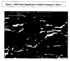
- SEM Figure 1
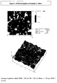
- AFM Figure 2
- Example 4 shows that the etch rate and the roughness values achieved can be further improved by the applying an accelerator (guadinium nitrate) within the etching solution.
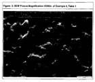
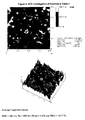
- the roughened copper surface resulting from treating a sample according to example 4 is shown in Figure 3 (SEM) and Figure 4 (AFM).
- the surface increase is 107,7% (RSAI, roughness surface area increase), an excellent value.
- RSAI values of higher than 60 % are required.
Abstract
Description
- The present invention relates to a method for treating copper or copper alloy surfaces for tight bonding to polymeric substrates, for example solder masks found in multilayer printed circuit boards. The substrate generally is a semiconductor-device, a lead frame or a printed circuit board.
- In manufacturing substrates like printed circuit boards, various steps are carried out in which copper or copper alloy surfaces must be tightly bonded to a polymeric substrate. In some cases, the required adhesion of the formed bonds must be ensured over a long period. In other cases, a tight bond only has to exist for a short period, e.g. when the polymeric substrate only remains on the copper or copper alloy surfaces during manufacture of the printed circuit board. For example, the tight bond of dry film resists (for structuring conductor lines on printed circuit boards) to the copper surfaces only has to exist while manufacturing the printed circuit board. After the conductor line structures are formed, the resists can be removed.
- Another application are solder masks, which are applied to a printed circuit board in order to retain a solderable surface on the board surface. Optimum solder mask resist performance can be only achieved if the printed circuit board surface is properly prepared prior to the application of the solder mask. The solder mask is designed to insulate and protect the copper traces of the printed circuit and keep them from shorting together during wave soldering or reflow soldering. In other words an insulating pattern is applied to a printed circuit board that exposes only the areas to be soldered.
- Solder mask options have changed radically in recent years, driven by the demands of surface mount assemblies, as well as environmental concerns, e.g. lead-free solder condition.
- With the advent of surface mounting and the introduction of fine pitch components, the requirements for the solder mask application have increased considerably. Due to the increasing complexity of the board circuitry (i.e. finer lines/spaces ratio) and the use of more selective finish techniques, proper adhesion of the solder mask has become a critical issue. Similarly, to withstand the thermal stress encountered during subsequent process steps, better adhesion of the solder mask is required.
- Commonly used mechanical pre-treatment processes like mechanical brushing or pumice do not match the desired criteria for optimum solder mask adhesion pre-treatment. Mechanical brushing cannot clean holes and leads to a directional finish often associated with a mechanical deformation. Whereas a pumice pre-treatment can cause residues on the copper surface and makes the rinsing critical in tight geometries.
- As a consequence, the need for chemical etching solutions as a pre-treatment step before application of polymeric materials like solder masks has increased during recent years.
- Generally, it is a challenge to provide chemical etching solutions to treat copper or copper alloy surfaces which only roughen the surface, but do not excessively etch away the copper layers. Several etching solutions have been developed to meet this need, but exhibit various disadvantages.
- Conventional and established treatment methods make use of sodium persulfate or hydrogen peroxide based etching solutions for copper surfaces. These solutions result in uniformly etched the copper surfaces, however only marginally increase the etched surface area. Generally, the lower the increase in surface area is, the poorer the adhesion properties of the subsequently formed bond between the metal and the polymeric substrate are.
- Therefore, such conventional etch composition do not yield etch results sufficient for fine line technology. This applies particularly to fine line high-density interconnect (HDI) feature on printed circuit board sizes of 50 µm and today even 25 µm or lower. The sizes particular relate to the US value. The US value determines the width of a conductor track (L) and the space (S) between two conductor tracks. Fine line applications are typically described by US-values of 50 µm or lower for the L and S-value, more particular 25 µm or lower for the L and S-value. In order to enable fine line technology the need for having a resolution with semi aqueous developable solder masks below 125 µm is increasing.
- Solder masks applied to such pre-treated copper surfaces show insufficient adhesion to the copper surface.
-
US 5,807,493 discloses a micro etching solution for copper or copper alloys containing a cupric ion source, an organic acid, a halide ion source and water resulting in adhesion improvement of resins or polymers on copper or copper alloy surfaces. -
EP 0855454 B 1 relates to a micro etching solution for copper or copper alloys comprising and oxidizing agent which is a cupric ion or ferric ion source, a polymer compound which contains polyamine chains or cationic group, water and a halide ion source. A micro roughened metal surface is gained by applying this process. - The use of cupric ions like cupric chloride, however, has some disadvantages. The use of cupric ions is expensive and the etch rate achieved is not sufficient for all applications desired for such process. If ferric salts like ferric chloride is used as the etch ingredient, unwanted precipitation and sludge formation of ferric ion compounds is often a problem, particularly when working at high ferric ion concentrations.
- Therefore, it is an object of the present invention to provide a method for an efficient pre-treatment of copper or copper alloys creating a tight bond between the copper surfaces and polymer surfaces applied thereto and avoiding the disadvantages of the state of the art.
- The process should be simple, easy to use, have a high etch rate, be inexpensive and creating no problems in the subsequent processing steps of the substrate, particularly a printed circuit board.
- This problem is solved by applying a solution to treat copper or copper alloy surfaces so that a tight bond can be subsequently formed between the copper or copper alloy surfaces and polymeric substrates by contacting the copper surfaces with a solution comprising:
- (i) a ferric ion source
- (ii) a buffer of an organic acid and an organic acid salt
- (iii) a halide ion source
- (iv) an accelerator
- The method according to this invention is carried out by contacting the copper or copper alloy surfaces with aforementioned solution. The substrate can be immersed into the solution or the solution can be sprayed onto the copper or copper alloy surface of the substrate. For this purpose common horizontal or vertical equipment can be utilized.
- Using a spray, the solution is sprayed onto the substrate having a copper or copper alloy surface at a pressure of 1 -10 bar.
- For both methods (spray or solution) the process is preferably carried out at a temperature of 20 - 60°C. The treatment time can vary between 15 and 300 s.
- The preferable ranges of the ingredients in the solution are:
Ferric ions 1 - 50 g/l, more preferred 3 -15 g/l Buffer 10 - 200 g/l Halide ion 1 - 100 g/l Accelerator 0,5 - 30 g/l, more preferred 1 - 10 g/l - Ferric ion sources can be ferric salts of inorganic acids such as ferric chloride, ferric nitrate, ferric sulfate, ferric bromide. Salts of organic acids such as ferric acetate and solutions such as ferric hydroxide may also be applied. Two or more ferric ion sources may be used together. The amount of the ferric compounds in terms of the content of metal ions is in the range of 1 - 50 g/l, preferably 3 - 15 g/l.
- The etching solution according to the invention operates at a fairly low ferric ion content. The low ferric ion concentration results in a moderate etch rate, yielding the desired roughness properties while avoiding excessive etching of the copper or copper alloy from the substrate.
- Buffer solutions applied in the current invention contain an organic acid and its corresponding salt, preferably its sodium salt. The amount of the acids is preferably in the range of 1 - 200 g/l, more preferred 1 - 50 g/l, the amount of the corresponding salt preferably in the range of 1- 200 g/l, more preferred 1 - 50 g/l. In order to achieve a good buffer capacity the ratio of the acid to the salt should range between 10 : 1 to 1 : 1. Examples for buffer solutions comprise formic acid / sodium formiate, tartaric acid / potassium-sodium tartrate, citric acid / sodium citrate, acetic acid / sodium acetate and oxalic acid / sodium oxalate and mixtures thereof.
- The etching solution further contains an accelerator selected from the group consisting of urea, thiourea, guanidinium salts, sulfosalicylic acid, niacine amide and amino acids like glycine, alanine, valine, leucine, iso-leucine and cystein. Furthermore, triazoles, benzotriazoles, imidazoles, benzimidazole, tetrazoles and isocyanates can be used as accelerators.
- The accelerators not only increase the etch rate and surface roughness, but also prevent smudge or residue formation on the substrate. The amount of the accelerator preferably ranges between 0.5 - 30 g/l. The buffer in combination with the accelerator does not only influence the etch rate, but furthermore greatly enhances the surface roughness of the treated copper or copper alloy substrate. It is believed that the accelerator compound absorbs onto the copper surface, thus influencing the etch rate on a sub-micron scale. This causes the imparted roughness to be several times greater than without such accelerator. The accelerator also directs the etching process to the copper or copper alloy grain boundaries, resulting in greatly increased etching on the boundaries compared to the etch rate away from these grain boundaries. This effect further increases the surface roughness achieved, which is much greater than expected for ferric ion solutions. This effect is surprising.
- The etching solution according to the present invention results in better roughness values and adhesion properties of the polymeric materials to the copper or copper alloys as for example with those described in
EP 0 855 454 . This better etching effect is particularly remarkable for the etching of the grain boundaries and so result in deeper crevices in the etched surface. - The halide ions are selected from the group consisting of chloride, bromide and fluoride. Chloride is most preferred. The amount of halide ions added preferably ranges from 0,5 - 100 g/l, more preferred 1 - 20 g/l.
- Optionally, the solution can additionally contain a complexing agent for ferric ions. They are particularly useful when the concentration of the ferric ions in the etching solution is at the higher end of the preferred ranged, i.e. higher than 20 g/I.
- The etching solution is free of a polymer compound which contains polyamine chains or a cationic group or both as described in
EP 0 855 454 , the concentration of which is difficult to control in industrial etching processes. - The chemical composition of the etching solution is maintained at a "steady state" (i.e. approximately constant copper ion concentration) during operation by employing "feed-and-bleed" replenishment. At the beginning of the etch process, the solution is virtually free of copper ions. Upon applying the etch composition, copper ions are dissolved from the metal substrate resulting in an increase in copper ions in the solution. It is necessary to maintain the copper ion concentration constant in order to ensure a reliable etching process of the surface. Therefore, a part of the etching solution is taken out of the process (bleed) and replaced with fresh etching solution (feed). The amount of etching solution to be replenished depends on the copper content and can be calculated according to the following equation:
- C (g/l): Cu concentration at steady state
- B (in l/m2 Cu surface) : bleed rate
- D (etch amount of Cu in g/m2): Dissolution of Cu by etch reaction

- The etch reaction is represented by the following equation:
Fe(III)Cl3 + Cu → Fe(II)Cl2 + Cu(I)Cl
- The copper ion concentration can be kept constant at a desired concentration by the before mentioned feed-and-bleed technology. In order to make the process cost efficient it is recommended to keep the copper ion concentration between 5 and 60 g/l, preferably 20 - 40 g/l. At this concentration the copper ions have no negative effect on the etching result.
- Since the etching solution of the invention is typically applied to the substrate as a spray, the ferric ions reduced to ferrous ions upon dissolving of the copper will be reoxidised by oxygen from the air. Therefore, the amount of ferric ions to be replenished is equal to the amount of ferric ions which are dragged out resulting in a cheap replenishment.
4 Fe (II) + O2 + 4 H⊕ → 4 Fe (III) + 2 H2O
- During this reaction protons are consumed in order to oxidize the ferrous (Fe-II) ions back to ferric (Fe-III) ions. The buffer applied in the etching solution maintain the pH-value within the desired range during operation. This ensures a constant etch rate. Generally, the lower the pH-value, the faster the etch rate or copper dissolution rate is. The concentration of the buffer system is adjusted as such that an etch rate appropriate for vertical or horizontal pre-treatment equipments is achieved. Upon choosing the concentrations given before, this aim is achieved. Standard tests (etch rates vs. buffer concentration) may be applied for different systems in order to determine the optimum etch rate. These experiments are common in industry and performed on a routine basis.
- After the copper or copper alloy surface has been treated as such, the copper or copper alloy surfaces are rinsed with water, e.g. deionised water and then dried, e.g. with hot air.
- Optionally, the etched copper or copper alloy surfaces can also be treated for 5 - 300 seconds with diluted acid after being rinsed, preferably with 10 weight% hydrochloric acid. After being treated with acid, the copper surfaces are again rinsed, preferably with deionised water.
- The samples are preferably treated by spraying the etching solution according to the invention onto the samples. The solution can be sprayed in a vertical mode or horizontal mode, depending on the equipment desired. Alternatively, the samples can be immersed into the etching solutions. To achieve the same roughness values compared to spraying, the solution needs to be penetrated by oxygen, e.g. by bubbling air through it.
- The etching solution of the invention also has the advantage to be compatible with commonly used solder masks and selective finish techniques, e.g. hot air solder level (HASL), immersion silver, electroless nickel gold (ENIG) and immersion tin.
- To illustrate the broad scope of this invention, ENIG and immersion tin are selected for sample preparation as selective finishes. The immersion of printed circuit boards into an electroless nickel gold process requires and excellent adhesion of the solder mask on the copper surface due to the relatively long treatment times and high process temperatures. The inevitable hydrogen evolution is also critical for solder mask adhesion. When applying immersion tin baths at higher temperatures, which generally contain thiourea and acids, attack of the bond between the solder mask and the copper surface is likely to occur. The better the adhesion properties between the solder mask and the copper, the less likely such an attack is.
- After roughening the samples with the solution according to the invention (see Table 1 for details) they were coated with a solder mask. An Elpemer SD 2467 DG solder mask was applied with a semi-automatic screen printer. The coated samples were pre-cured for 40 minutes at 80°C.
- A test pattern (Test Coupon G of IPC-2221) was created by using a UV exposure (Stouffer Step 11-12) followed by an aqueous alkaline image development in a 1 % sodium carbonate solution at 30°C in a spray module.
- The test samples were rinsed with city water and finally rinsed with DI water. Afterwards the panels were dried and the final cure was done at 150°C for 60 minutes. After the final cure the test samples were cut in half and treated either in an immersion tin process for 10 min at 65 °C (commercially available Stannatech process from Atotech Deutschland GmbH) or an electroless nickel-gold process (commercially available Aurotech process from Atotech Deutschland GmbH) consisting of an electroless nickel plating for 20 min at 80 °C and an immersion gold plating for 8 min at 85 °C. After 1 hour holding time, the adhesion of the solder mask on the roughened copper surface was tested by making a tape test in relation to IPC TM-650 Number 2.4.28.1. The results are given in Table 1.
- The following samples were made according to the previous described process sequence in order to illustrate the invention. Test solutions were prepared according to the composition shown in Table 1. After etching test coupons were processed with the process sequence as described before. The results after tape test are shown in Table 1. Only adhesion values between the solder mask on the copper surfaces are considered suitable which pass both final finish applications ENIG and immersion tin. For such treated samples the adhesion between the solder mask and the copper surface is strong enough to be considered universally applicable.
- Example 1 and example 2 contain a buffer system and a halide ion source. According to the tape test result, the copper surface roughness achieved does not provide a sufficient adhesion of the solder mask for both ENIG- and immersion tin-finish techniques. Example 2 showed an improvement compared to example 1 by changing the halide ion source from hydrochloric acid to sodium chloride. These two pre-treatment solutions would not be considered suitable for solder mask applications.
- Example 3 contains a different buffer composition resulting in a more roughened copper surface shown in Figure 1 (SEM) and Figure 2 (AFM) by the following values: RSAI value (roughness surface area increase) = 41,9 %, RMS (root mean square value of depths of etched crevices) = 164 nm, Ra (average roughness value) = 132 nm and Rmax = 1157 nm. However, example 3 did only pass the tape test after ENIG, not after immersion tin. Therefore, it would not be considered suitable for the application of the present invention.
- Example 4 shows that the etch rate and the roughness values achieved can be further improved by the applying an accelerator (guadinium nitrate) within the etching solution. The roughened copper surface resulting from treating a sample according to example 4 is shown in Figure 3 (SEM) and Figure 4 (AFM). Figure 4 shows very good surface roughness parameters: RMS (root mean square value of depths of etched crevices) = 342 nm, Ra (average roughness value) = 289 nm, Rmax = 1878 nm. The surface increase is 107,7% (RSAI, roughness surface area increase), an excellent value. Generally, for solder mask applications, RSAI values of higher than 60 % are required. For other application the present invention is suitable for, RSAI values of higher than 45 % are often sufficient.
Table 1 Component wt.% Tape Test results after Selective Finish ENIG / Tin Copper surface appearance Etch depth [µm] 30 s / 60 s Example 1 (comparative) Ferric chloride 1,2 Failed/Failed Less rough Dark appearance 2.2/4.4 Citric acid 12 Sodium citrate 15 HCl (32%) 4 DI water 67,8 Example 2 (comparative) Ferric chloride 1.2 Passed/Failed Rough Salmon pink 2.0/4.0 Citric acid 12 Sodium citrate 15 NaCl 5 DI water 66,8 Example 3 (comparative) Ferric chloride 1.2 Passed/Failed Rough Salmon pink 0,8/1,7 Gluconic acid 10 Sodiumgluconate 15 NaCl 1 DI water 72,8 Example 4 Ferric chloride 1.2 Passed/Passed Rough Salmon pink 1,4/2,8 Gluconic acid 10 Sodiumgluconate 15 NaCl 1 Guanidinium nitrate 0,5 DI water 73,5
Claims (13)
- A solution to treat copper or copper alloy surfaces so that a tight bond can be subsequently formed between the copper or copper alloy surfaces and polymeric substrates by contacting the copper surfaces with a solution comprising:(i) a ferric ion source(ii) a buffer of an organic acid and its corresponding salt(iii) a halide ion source(iv) an acceleratorwherein the accelerator is selected from the group consisting of urea, thiourea, guanidinium salts, sulfosalicylic acid, niacine amide, cyanates, thiocyanates, triazoles, benzotriazoles, imidazoles, benzimidazoles, tetrazoles, isocyanates and amino acids.
- A solution according to claim 1 wherein the ferric ion source is selected from the group consisting of ferric chloride, ferric nitrate, ferric sulfate, ferric bromide; ferric acetate ferric hydroxide.
- A solution according to any of the foregoing claims wherein the ferric ion concentration is in the range of 5 - 50 g/l.
- A solution according to any of the foregoing claims wherein the buffer is selected from the group consisting of formic acid / sodium formiate, tartaric acid / potassium-sodium tartrate, citric acid / sodium citrate, acetic acid / sodium acetate and oxalic acid / sodium oxalate.
- A solution according to any of the foregoing claims wherein the buffer concentration is in the range of 5 - 200 g/l for the acid and of 1 - 200 g/l for its corresponding salt.
- A solution according to any of the foregoing claims wherein the accelerator concentration is in the range of 0,5 - 30 g/l, more preferred 1 -10 g/l.
- A solution according to any of the foregoing claims wherein the halide ion concentration is in the range of 5 -30 g/l
- A method to treat copper or copper alloy surfaces so that a tight bond can be subsequently formed between the copper or copper alloy surfaces and polymeric substrates by contacting the copper surfaces with a solution according to one of the claims 1 - 12.
- A method according to claim 8 wherein the temperature is between 20 - 60°C.
- A method according to claim 8 wherein the treatment time is between 15 and 300 s.
- A method according to the claims 9 and 10 wherein the solution is sprayed onto the substrate having a copper or copper alloy surface at a pressure of preferably 1 - 10 bar.
- A method according to any of the foregoing claims wherein the copper ion concentration is maintained constant in a range between 5 - 60 g/l Cu2+ by taking a part of the etching solution out of the process (bleed) and replaced it by fresh etching solution (feed) and whereby the amount of etching solution to be replenished is calculated according to the following equation:
 wherein C is the Cu2+ concentration in the steady state in g/lB is the bleed rate in I/m2 Cu2+ surfaceD (etch amount of Cu in g/m2): Dissolution of Cu by etching reaction
 - Use of the solution according to any of the foregoing claims for the treatment of printed circuit boards, which have copper layers, for the formation of a firmly adhesive bonding between the printed circuit board and a solder mask applied thereto.
Priority Applications (10)
| Application Number | Priority Date | Filing Date | Title |
|---|---|---|---|
| ES05023278T ES2348361T3 (en) | 2005-10-25 | 2005-10-25 | METHOD FOR IMPROVED ADHESION OF POLYMER MATERIALS TO COPPER SURFACES OR COPPER ALLOYS. |
| DE602005023739T DE602005023739D1 (en) | 2005-10-25 | 2005-10-25 | Composition and method of improving the adhesion of the polymeric materials to copper or copper alloy surfaces |
| AT05023278T ATE482303T1 (en) | 2005-10-25 | 2005-10-25 | COMPOSITION AND METHOD FOR IMPROVING ADHESION OF POLYMERIC MATERIALS ON COPPER OR COPPER ALLOY SURFACES |
| EP05023278A EP1780309B8 (en) | 2005-10-25 | 2005-10-25 | Composition and method for improved adhesion of polymeric materials to copper or copper alloy surfaces |
| TW095133091A TWI395837B (en) | 2005-10-25 | 2006-09-07 | Method for improved adhesion of polymeric materials to copper or copper alloy surfaces |
| PCT/EP2006/010201 WO2007048559A1 (en) | 2005-10-25 | 2006-10-23 | Composition and method for improved adhesion of polymeric materials to copper or copper alloy surfaces |
| CNA2006800391032A CN101379219A (en) | 2005-10-25 | 2006-10-23 | Composition and method for improved adhesion of polymeric materials to copper or copper alloy surfaces |
| JP2008536981A JP2009512784A (en) | 2005-10-25 | 2006-10-23 | Compositions and methods for improving adhesion of polymeric materials to copper or copper alloy surfaces |
| KR1020087012280A KR20080072866A (en) | 2005-10-25 | 2006-10-23 | Composition and method for improved adhesion of polymeric materials to copper or copper alloy surfaces |
| US12/090,990 US8192636B2 (en) | 2005-10-25 | 2006-10-23 | Composition and method for improved adhesion of polymeric materials to copper alloy surfaces |
Applications Claiming Priority (1)
| Application Number | Priority Date | Filing Date | Title |
|---|---|---|---|
| EP05023278A EP1780309B8 (en) | 2005-10-25 | 2005-10-25 | Composition and method for improved adhesion of polymeric materials to copper or copper alloy surfaces |
Publications (3)
| Publication Number | Publication Date |
|---|---|
| EP1780309A1 true EP1780309A1 (en) | 2007-05-02 |
| EP1780309B1 EP1780309B1 (en) | 2010-09-22 |
| EP1780309B8 EP1780309B8 (en) | 2010-12-15 |
Family
ID=36072010
Family Applications (1)
| Application Number | Title | Priority Date | Filing Date |
|---|---|---|---|
| EP05023278A Not-in-force EP1780309B8 (en) | 2005-10-25 | 2005-10-25 | Composition and method for improved adhesion of polymeric materials to copper or copper alloy surfaces |
Country Status (10)
| Country | Link |
|---|---|
| US (1) | US8192636B2 (en) |
| EP (1) | EP1780309B8 (en) |
| JP (1) | JP2009512784A (en) |
| KR (1) | KR20080072866A (en) |
| CN (1) | CN101379219A (en) |
| AT (1) | ATE482303T1 (en) |
| DE (1) | DE602005023739D1 (en) |
| ES (1) | ES2348361T3 (en) |
| TW (1) | TWI395837B (en) |
| WO (1) | WO2007048559A1 (en) |
Cited By (3)
| Publication number | Priority date | Publication date | Assignee | Title |
|---|---|---|---|---|
| EP2241653A1 (en) * | 2009-04-15 | 2010-10-20 | ATOTECH Deutschland GmbH | Composition and method for micro etching of copper and copper alloys |
| WO2013048834A1 (en) * | 2011-09-30 | 2013-04-04 | 3M Innovative Properties Company | Methods of continuously wet etching a patterned substrate |
| CN104746091A (en) * | 2015-04-28 | 2015-07-01 | 深圳市崇辉表面技术开发有限公司 | Cast aluminum alloy white washing descaling solution |
Families Citing this family (13)
| Publication number | Priority date | Publication date | Assignee | Title |
|---|---|---|---|---|
| US20100155260A1 (en) * | 2008-12-22 | 2010-06-24 | Kwan Yiu Fai | Micro-blasting treatment for lead frames |
| KR20100091663A (en) | 2009-02-11 | 2010-08-19 | 삼성전자주식회사 | Surface modifying agent, laminated structure using the same, method of manufacturing the structure, and transistor including the same |
| CN101525745B (en) * | 2009-04-03 | 2011-03-30 | 四川大学 | Metal surface treatment agent and printed wiring board with protecting film formed thereby |
| CN102822390B (en) * | 2010-05-26 | 2014-11-26 | 安美特德国有限公司 | Composition and method for micro etching of copper and copper alloys |
| EP2754732B1 (en) * | 2013-01-15 | 2015-03-11 | ATOTECH Deutschland GmbH | Aqueous composition for etching of copper and copper alloys |
| EP2862959A1 (en) * | 2013-10-21 | 2015-04-22 | ATOTECH Deutschland GmbH | Method of selectively treating copper in the presence of further metal |
| US9472420B2 (en) | 2013-12-20 | 2016-10-18 | Air Products And Chemicals, Inc. | Composition for titanium nitride hard mask and etch residue removal |
| CN104294273B (en) * | 2014-11-08 | 2016-09-21 | 汕头超声印制板(二厂)有限公司 | A kind of nontoxic stripping gold liquid and the method being applied to printed circuit board detection thereof |
| TWI585841B (en) * | 2015-02-06 | 2017-06-01 | 國立台灣科技大學 | Substrate, method for processing the same and apparatus for processing the same |
| CN107267971B (en) * | 2017-05-25 | 2019-11-26 | 中信大锰矿业有限责任公司 | A kind of passivator and preparation method thereof of without phosphorus Chrome-free |
| JP6333455B1 (en) * | 2017-08-23 | 2018-05-30 | メック株式会社 | Copper microetching agent and method of manufacturing wiring board |
| CN114045494B (en) * | 2021-10-25 | 2023-02-03 | 深圳前海榕达创途化工科技股份有限公司 | Low-acidity etching production method for PCB and two-liquid type acidic etching liquid system |
| CN114457335B (en) * | 2022-02-15 | 2023-10-27 | 江西省科学院应用物理研究所 | Metallographic etchant for copper-iron-carbon alloy and use method thereof |
Citations (15)
| Publication number | Priority date | Publication date | Assignee | Title |
|---|---|---|---|---|
| GB1154015A (en) * | 1966-08-22 | 1969-06-04 | Photo Engravers Res Inst Inc | Etching of Printed Circuit Components |
| JPS5330435A (en) * | 1976-09-02 | 1978-03-22 | Sumitomo Metal Mining Co | Etching liquid |
| US4374744A (en) * | 1981-04-06 | 1983-02-22 | Mec Co., Ltd. | Stripping solution for tin or tin alloys |
| US4921571A (en) * | 1989-07-28 | 1990-05-01 | Macdermid, Incorporated | Inhibited composition and method for stripping tin, lead or tin-lead alloy from copper surfaces |
| DE4118764A1 (en) * | 1991-06-07 | 1992-12-10 | Chema Technologien Gmbh | Organic additives for ferric chloride-contg. copper@ etch solns. - comprising complex-forming organic acids which prevent sludge formation |
| US5244539A (en) * | 1992-01-27 | 1993-09-14 | Ardrox, Inc. | Composition and method for stripping films from printed circuit boards |
| US5505872A (en) * | 1995-05-23 | 1996-04-09 | Applied Electroless Concepts, Inc. | Solder stripper recycle and reuse |
| US5512201A (en) * | 1995-02-13 | 1996-04-30 | Applied Chemical Technologies, Inc. | Solder and tin stripper composition |
| EP0791671A1 (en) * | 1996-02-26 | 1997-08-27 | Shikoku Chemicals Corporation | Surface treating agent for copper or copper alloy |
| EP0826793A1 (en) * | 1996-08-30 | 1998-03-04 | MEC CO., Ltd. | Composition for stripping tin or tin alloys |
| US5741432A (en) * | 1995-01-17 | 1998-04-21 | The Dexter Corporation | Stabilized nitric acid compositions |
| WO1998033951A1 (en) * | 1997-01-31 | 1998-08-06 | Taylor James M | Composition and method for priming substrate materials |
| US5989449A (en) * | 1995-08-30 | 1999-11-23 | Morton International, Inc. | Composition and method for stripping tin and tin-lead from copper surfaces |
| US20050126588A1 (en) * | 2003-11-04 | 2005-06-16 | Carter Melvin K. | Chemical mechanical polishing slurries and cleaners containing salicylic acid as a corrosion inhibitor |
| US20050178742A1 (en) * | 2003-11-10 | 2005-08-18 | Chelle Philippe H. | Compositions and methods for rapidly removing overfilled substrates |
Family Cites Families (4)
| Publication number | Priority date | Publication date | Assignee | Title |
|---|---|---|---|---|
| JP2923524B2 (en) * | 1995-08-01 | 1999-07-26 | メック株式会社 | Copper and copper alloy microetching agent and microetching method |
| JP3458023B2 (en) | 1995-08-01 | 2003-10-20 | メック株式会社 | Copper and copper alloy microetchants |
| JP2000282265A (en) * | 1999-03-31 | 2000-10-10 | Mec Kk | Microetching agent for copper or copper alloy and surface treating method using the same |
| EP1272580A2 (en) * | 2000-04-11 | 2003-01-08 | Cabot Microelectronics Corporation | System for the preferential removal of silicon oxide |
-
2005
- 2005-10-25 ES ES05023278T patent/ES2348361T3/en active Active
- 2005-10-25 AT AT05023278T patent/ATE482303T1/en active
- 2005-10-25 EP EP05023278A patent/EP1780309B8/en not_active Not-in-force
- 2005-10-25 DE DE602005023739T patent/DE602005023739D1/en active Active
-
2006
- 2006-09-07 TW TW095133091A patent/TWI395837B/en not_active IP Right Cessation
- 2006-10-23 WO PCT/EP2006/010201 patent/WO2007048559A1/en active Application Filing
- 2006-10-23 JP JP2008536981A patent/JP2009512784A/en active Pending
- 2006-10-23 CN CNA2006800391032A patent/CN101379219A/en active Pending
- 2006-10-23 US US12/090,990 patent/US8192636B2/en not_active Expired - Fee Related
- 2006-10-23 KR KR1020087012280A patent/KR20080072866A/en not_active Application Discontinuation
Patent Citations (16)
| Publication number | Priority date | Publication date | Assignee | Title |
|---|---|---|---|---|
| GB1154015A (en) * | 1966-08-22 | 1969-06-04 | Photo Engravers Res Inst Inc | Etching of Printed Circuit Components |
| JPS5330435A (en) * | 1976-09-02 | 1978-03-22 | Sumitomo Metal Mining Co | Etching liquid |
| US4374744A (en) * | 1981-04-06 | 1983-02-22 | Mec Co., Ltd. | Stripping solution for tin or tin alloys |
| US4921571A (en) * | 1989-07-28 | 1990-05-01 | Macdermid, Incorporated | Inhibited composition and method for stripping tin, lead or tin-lead alloy from copper surfaces |
| US4921571B1 (en) * | 1989-07-28 | 1991-12-31 | Macdermid Inc | |
| DE4118764A1 (en) * | 1991-06-07 | 1992-12-10 | Chema Technologien Gmbh | Organic additives for ferric chloride-contg. copper@ etch solns. - comprising complex-forming organic acids which prevent sludge formation |
| US5244539A (en) * | 1992-01-27 | 1993-09-14 | Ardrox, Inc. | Composition and method for stripping films from printed circuit boards |
| US5741432A (en) * | 1995-01-17 | 1998-04-21 | The Dexter Corporation | Stabilized nitric acid compositions |
| US5512201A (en) * | 1995-02-13 | 1996-04-30 | Applied Chemical Technologies, Inc. | Solder and tin stripper composition |
| US5505872A (en) * | 1995-05-23 | 1996-04-09 | Applied Electroless Concepts, Inc. | Solder stripper recycle and reuse |
| US5989449A (en) * | 1995-08-30 | 1999-11-23 | Morton International, Inc. | Composition and method for stripping tin and tin-lead from copper surfaces |
| EP0791671A1 (en) * | 1996-02-26 | 1997-08-27 | Shikoku Chemicals Corporation | Surface treating agent for copper or copper alloy |
| EP0826793A1 (en) * | 1996-08-30 | 1998-03-04 | MEC CO., Ltd. | Composition for stripping tin or tin alloys |
| WO1998033951A1 (en) * | 1997-01-31 | 1998-08-06 | Taylor James M | Composition and method for priming substrate materials |
| US20050126588A1 (en) * | 2003-11-04 | 2005-06-16 | Carter Melvin K. | Chemical mechanical polishing slurries and cleaners containing salicylic acid as a corrosion inhibitor |
| US20050178742A1 (en) * | 2003-11-10 | 2005-08-18 | Chelle Philippe H. | Compositions and methods for rapidly removing overfilled substrates |
Non-Patent Citations (1)
| Title |
|---|
| DATABASE WPI Section Ch Week 197818, Derwent World Patents Index; Class L03, AN 1978-32691A, XP002374572 * |
Cited By (4)
| Publication number | Priority date | Publication date | Assignee | Title |
|---|---|---|---|---|
| EP2241653A1 (en) * | 2009-04-15 | 2010-10-20 | ATOTECH Deutschland GmbH | Composition and method for micro etching of copper and copper alloys |
| WO2013048834A1 (en) * | 2011-09-30 | 2013-04-04 | 3M Innovative Properties Company | Methods of continuously wet etching a patterned substrate |
| US9301397B2 (en) | 2011-09-30 | 2016-03-29 | 3M Innovative Properties Company | Methods of continuously wet etching a patterned substrate |
| CN104746091A (en) * | 2015-04-28 | 2015-07-01 | 深圳市崇辉表面技术开发有限公司 | Cast aluminum alloy white washing descaling solution |
Also Published As
| Publication number | Publication date |
|---|---|
| EP1780309B8 (en) | 2010-12-15 |
| EP1780309B1 (en) | 2010-09-22 |
| ATE482303T1 (en) | 2010-10-15 |
| DE602005023739D1 (en) | 2010-11-04 |
| WO2007048559A1 (en) | 2007-05-03 |
| CN101379219A (en) | 2009-03-04 |
| TWI395837B (en) | 2013-05-11 |
| US8192636B2 (en) | 2012-06-05 |
| US20100035435A1 (en) | 2010-02-11 |
| TW200720483A (en) | 2007-06-01 |
| JP2009512784A (en) | 2009-03-26 |
| KR20080072866A (en) | 2008-08-07 |
| ES2348361T3 (en) | 2010-12-03 |
Similar Documents
| Publication | Publication Date | Title |
|---|---|---|
| EP1780309B1 (en) | Composition and method for improved adhesion of polymeric materials to copper or copper alloy surfaces | |
| USRE45175E1 (en) | Process for silver plating in printed circuit board manufacture | |
| EP0855454B1 (en) | Microetching composition for copper or copper alloy | |
| US5807493A (en) | Microetching method for copper or copper alloy | |
| EP0670379B1 (en) | Method for microetching copper or copper alloy surfaces | |
| US6395329B2 (en) | Printed circuit board manufacture | |
| EP2878705B1 (en) | Microetching agent for copper, replenishment solution thereof, and method for producing wiring board | |
| US6319543B1 (en) | Process for silver plating in printed circuit board manufacture | |
| EP3680363B1 (en) | Microetching agent for copper, copper surface roughening method and wiring board production method | |
| KR19990013630A (en) | Micro Etching Agent of Copper and Copper Alloy | |
| EP3498884A1 (en) | Pretreating liquid for electroless plating to be used during reduction treatment, and process for producing printed wiring board | |
| EP1920026A1 (en) | Improved microetching solution | |
| JP3337802B2 (en) | Direct plating method by metallization of copper (I) oxide colloid | |
| EP3060696B1 (en) | Method of selectively treating copper in the presence of further metal | |
| WO2008005094A2 (en) | Process for increasing the adhesion of a metal surface to a polymer | |
| JP2007262394A (en) | Surface-treating agent |
Legal Events
| Date | Code | Title | Description |
|---|---|---|---|
| PUAI | Public reference made under article 153(3) epc to a published international application that has entered the european phase |
Free format text: ORIGINAL CODE: 0009012 |
|
| 17P | Request for examination filed |
Effective date: 20060724 |
|
| AK | Designated contracting states |
Kind code of ref document: A1 Designated state(s): AT BE BG CH CY CZ DE DK EE ES FI FR GB GR HU IE IS IT LI LT LU LV MC NL PL PT RO SE SI SK TR |
|
| AX | Request for extension of the european patent |
Extension state: AL BA HR MK YU |
|
| AKX | Designation fees paid |
Designated state(s): AT BE BG CH CY CZ DE DK EE ES FI FR GB GR HU IE IS IT LI LT LU LV MC NL PL PT RO SE SI SK TR |
|
| GRAP | Despatch of communication of intention to grant a patent |
Free format text: ORIGINAL CODE: EPIDOSNIGR1 |
|
| GRAS | Grant fee paid |
Free format text: ORIGINAL CODE: EPIDOSNIGR3 |
|
| GRAA | (expected) grant |
Free format text: ORIGINAL CODE: 0009210 |
|
| AK | Designated contracting states |
Kind code of ref document: B1 Designated state(s): AT BE BG CH CY CZ DE DK EE ES FI FR GB GR HU IE IS IT LI LT LU LV MC NL PL PT RO SE SI SK TR |
|
| REG | Reference to a national code |
Ref country code: GB Ref legal event code: FG4D |
|
| REG | Reference to a national code |
Ref country code: CH Ref legal event code: EP |
|
| REG | Reference to a national code |
Ref country code: IE Ref legal event code: FG4D |
|
| REF | Corresponds to: |
Ref document number: 602005023739 Country of ref document: DE Date of ref document: 20101104 Kind code of ref document: P |
|
| RIN2 | Information on inventor provided after grant (corrected) |
Inventor name: TEWS, DIRK DR. Inventor name: SPARING, CHRISTIAN |
|
| REG | Reference to a national code |
Ref country code: ES Ref legal event code: FG2A Effective date: 20101123 |
|
| PG25 | Lapsed in a contracting state [announced via postgrant information from national office to epo] |
Ref country code: FI Free format text: LAPSE BECAUSE OF FAILURE TO SUBMIT A TRANSLATION OF THE DESCRIPTION OR TO PAY THE FEE WITHIN THE PRESCRIBED TIME-LIMIT Effective date: 20100922 Ref country code: LT Free format text: LAPSE BECAUSE OF FAILURE TO SUBMIT A TRANSLATION OF THE DESCRIPTION OR TO PAY THE FEE WITHIN THE PRESCRIBED TIME-LIMIT Effective date: 20100922 |
|
| REG | Reference to a national code |
Ref country code: NL Ref legal event code: VDEP Effective date: 20100922 |
|
| LTIE | Lt: invalidation of european patent or patent extension |
Effective date: 20100922 |
|
| PG25 | Lapsed in a contracting state [announced via postgrant information from national office to epo] |
Ref country code: PL Free format text: LAPSE BECAUSE OF FAILURE TO SUBMIT A TRANSLATION OF THE DESCRIPTION OR TO PAY THE FEE WITHIN THE PRESCRIBED TIME-LIMIT Effective date: 20100922 Ref country code: SI Free format text: LAPSE BECAUSE OF FAILURE TO SUBMIT A TRANSLATION OF THE DESCRIPTION OR TO PAY THE FEE WITHIN THE PRESCRIBED TIME-LIMIT Effective date: 20100922 |
|
| PG25 | Lapsed in a contracting state [announced via postgrant information from national office to epo] |
Ref country code: GR Free format text: LAPSE BECAUSE OF FAILURE TO SUBMIT A TRANSLATION OF THE DESCRIPTION OR TO PAY THE FEE WITHIN THE PRESCRIBED TIME-LIMIT Effective date: 20101223 Ref country code: SE Free format text: LAPSE BECAUSE OF FAILURE TO SUBMIT A TRANSLATION OF THE DESCRIPTION OR TO PAY THE FEE WITHIN THE PRESCRIBED TIME-LIMIT Effective date: 20100922 Ref country code: LV Free format text: LAPSE BECAUSE OF FAILURE TO SUBMIT A TRANSLATION OF THE DESCRIPTION OR TO PAY THE FEE WITHIN THE PRESCRIBED TIME-LIMIT Effective date: 20100922 |
|
| PG25 | Lapsed in a contracting state [announced via postgrant information from national office to epo] |
Ref country code: NL Free format text: LAPSE BECAUSE OF FAILURE TO SUBMIT A TRANSLATION OF THE DESCRIPTION OR TO PAY THE FEE WITHIN THE PRESCRIBED TIME-LIMIT Effective date: 20100922 Ref country code: SK Free format text: LAPSE BECAUSE OF FAILURE TO SUBMIT A TRANSLATION OF THE DESCRIPTION OR TO PAY THE FEE WITHIN THE PRESCRIBED TIME-LIMIT Effective date: 20100922 Ref country code: PT Free format text: LAPSE BECAUSE OF FAILURE TO SUBMIT A TRANSLATION OF THE DESCRIPTION OR TO PAY THE FEE WITHIN THE PRESCRIBED TIME-LIMIT Effective date: 20110124 Ref country code: RO Free format text: LAPSE BECAUSE OF FAILURE TO SUBMIT A TRANSLATION OF THE DESCRIPTION OR TO PAY THE FEE WITHIN THE PRESCRIBED TIME-LIMIT Effective date: 20100922 Ref country code: EE Free format text: LAPSE BECAUSE OF FAILURE TO SUBMIT A TRANSLATION OF THE DESCRIPTION OR TO PAY THE FEE WITHIN THE PRESCRIBED TIME-LIMIT Effective date: 20100922 Ref country code: IS Free format text: LAPSE BECAUSE OF FAILURE TO SUBMIT A TRANSLATION OF THE DESCRIPTION OR TO PAY THE FEE WITHIN THE PRESCRIBED TIME-LIMIT Effective date: 20110122 Ref country code: CZ Free format text: LAPSE BECAUSE OF FAILURE TO SUBMIT A TRANSLATION OF THE DESCRIPTION OR TO PAY THE FEE WITHIN THE PRESCRIBED TIME-LIMIT Effective date: 20100922 Ref country code: MC Free format text: LAPSE BECAUSE OF NON-PAYMENT OF DUE FEES Effective date: 20101031 |
|
| REG | Reference to a national code |
Ref country code: CH Ref legal event code: PL |
|
| PG25 | Lapsed in a contracting state [announced via postgrant information from national office to epo] |
Ref country code: BE Free format text: LAPSE BECAUSE OF FAILURE TO SUBMIT A TRANSLATION OF THE DESCRIPTION OR TO PAY THE FEE WITHIN THE PRESCRIBED TIME-LIMIT Effective date: 20100922 |
|
| PG25 | Lapsed in a contracting state [announced via postgrant information from national office to epo] |
Ref country code: CH Free format text: LAPSE BECAUSE OF NON-PAYMENT OF DUE FEES Effective date: 20101031 Ref country code: LI Free format text: LAPSE BECAUSE OF NON-PAYMENT OF DUE FEES Effective date: 20101031 |
|
| PLBE | No opposition filed within time limit |
Free format text: ORIGINAL CODE: 0009261 |
|
| STAA | Information on the status of an ep patent application or granted ep patent |
Free format text: STATUS: NO OPPOSITION FILED WITHIN TIME LIMIT |
|
| GBPC | Gb: european patent ceased through non-payment of renewal fee |
Effective date: 20101222 |
|
| 26N | No opposition filed |
Effective date: 20110623 |
|
| PG25 | Lapsed in a contracting state [announced via postgrant information from national office to epo] |
Ref country code: DK Free format text: LAPSE BECAUSE OF FAILURE TO SUBMIT A TRANSLATION OF THE DESCRIPTION OR TO PAY THE FEE WITHIN THE PRESCRIBED TIME-LIMIT Effective date: 20100922 |
|
| REG | Reference to a national code |
Ref country code: DE Ref legal event code: R097 Ref document number: 602005023739 Country of ref document: DE Effective date: 20110623 |
|
| PG25 | Lapsed in a contracting state [announced via postgrant information from national office to epo] |
Ref country code: IE Free format text: LAPSE BECAUSE OF NON-PAYMENT OF DUE FEES Effective date: 20101025 |
|
| PG25 | Lapsed in a contracting state [announced via postgrant information from national office to epo] |
Ref country code: GB Free format text: LAPSE BECAUSE OF NON-PAYMENT OF DUE FEES Effective date: 20101222 |
|
| PG25 | Lapsed in a contracting state [announced via postgrant information from national office to epo] |
Ref country code: CY Free format text: LAPSE BECAUSE OF FAILURE TO SUBMIT A TRANSLATION OF THE DESCRIPTION OR TO PAY THE FEE WITHIN THE PRESCRIBED TIME-LIMIT Effective date: 20100922 |
|
| PG25 | Lapsed in a contracting state [announced via postgrant information from national office to epo] |
Ref country code: HU Free format text: LAPSE BECAUSE OF FAILURE TO SUBMIT A TRANSLATION OF THE DESCRIPTION OR TO PAY THE FEE WITHIN THE PRESCRIBED TIME-LIMIT Effective date: 20110323 Ref country code: LU Free format text: LAPSE BECAUSE OF NON-PAYMENT OF DUE FEES Effective date: 20101025 Ref country code: BG Free format text: LAPSE BECAUSE OF FAILURE TO SUBMIT A TRANSLATION OF THE DESCRIPTION OR TO PAY THE FEE WITHIN THE PRESCRIBED TIME-LIMIT Effective date: 20100922 |
|
| PG25 | Lapsed in a contracting state [announced via postgrant information from national office to epo] |
Ref country code: TR Free format text: LAPSE BECAUSE OF FAILURE TO SUBMIT A TRANSLATION OF THE DESCRIPTION OR TO PAY THE FEE WITHIN THE PRESCRIBED TIME-LIMIT Effective date: 20100922 |
|
| PGFP | Annual fee paid to national office [announced via postgrant information from national office to epo] |
Ref country code: FR Payment date: 20121031 Year of fee payment: 8 |
|
| PGFP | Annual fee paid to national office [announced via postgrant information from national office to epo] |
Ref country code: ES Payment date: 20121026 Year of fee payment: 8 Ref country code: IT Payment date: 20121024 Year of fee payment: 8 |
|
| PG25 | Lapsed in a contracting state [announced via postgrant information from national office to epo] |
Ref country code: BG Free format text: LAPSE BECAUSE OF FAILURE TO SUBMIT A TRANSLATION OF THE DESCRIPTION OR TO PAY THE FEE WITHIN THE PRESCRIBED TIME-LIMIT Effective date: 20101222 |
|
| PGFP | Annual fee paid to national office [announced via postgrant information from national office to epo] |
Ref country code: AT Payment date: 20131011 Year of fee payment: 9 |
|
| REG | Reference to a national code |
Ref country code: FR Ref legal event code: ST Effective date: 20140630 |
|
| PG25 | Lapsed in a contracting state [announced via postgrant information from national office to epo] |
Ref country code: FR Free format text: LAPSE BECAUSE OF NON-PAYMENT OF DUE FEES Effective date: 20131031 Ref country code: IT Free format text: LAPSE BECAUSE OF NON-PAYMENT OF DUE FEES Effective date: 20131025 |
|
| REG | Reference to a national code |
Ref country code: AT Ref legal event code: MM01 Ref document number: 482303 Country of ref document: AT Kind code of ref document: T Effective date: 20141025 |
|
| REG | Reference to a national code |
Ref country code: ES Ref legal event code: FD2A Effective date: 20150709 |
|
| PG25 | Lapsed in a contracting state [announced via postgrant information from national office to epo] |
Ref country code: ES Free format text: LAPSE BECAUSE OF NON-PAYMENT OF DUE FEES Effective date: 20131026 |
|
| PG25 | Lapsed in a contracting state [announced via postgrant information from national office to epo] |
Ref country code: AT Free format text: LAPSE BECAUSE OF NON-PAYMENT OF DUE FEES Effective date: 20141025 |
|
| PGFP | Annual fee paid to national office [announced via postgrant information from national office to epo] |
Ref country code: DE Payment date: 20191021 Year of fee payment: 15 |
|
| REG | Reference to a national code |
Ref country code: DE Ref legal event code: R119 Ref document number: 602005023739 Country of ref document: DE |
|
| PG25 | Lapsed in a contracting state [announced via postgrant information from national office to epo] |
Ref country code: DE Free format text: LAPSE BECAUSE OF NON-PAYMENT OF DUE FEES Effective date: 20210501 |