EP1783844A2 - Phase change memory cell including multiple phase change material portions - Google Patents
Phase change memory cell including multiple phase change material portions Download PDFInfo
- Publication number
- EP1783844A2 EP1783844A2 EP06021708A EP06021708A EP1783844A2 EP 1783844 A2 EP1783844 A2 EP 1783844A2 EP 06021708 A EP06021708 A EP 06021708A EP 06021708 A EP06021708 A EP 06021708A EP 1783844 A2 EP1783844 A2 EP 1783844A2
- Authority
- EP
- European Patent Office
- Prior art keywords
- phase
- change material
- memory cell
- electrode
- change
- Prior art date
- Legal status (The legal status is an assumption and is not a legal conclusion. Google has not performed a legal analysis and makes no representation as to the accuracy of the status listed.)
- Granted
Links
Images

Classifications
-
- H—ELECTRICITY
- H10—SEMICONDUCTOR DEVICES; ELECTRIC SOLID-STATE DEVICES NOT OTHERWISE PROVIDED FOR
- H10N—ELECTRIC SOLID-STATE DEVICES NOT OTHERWISE PROVIDED FOR
- H10N70/00—Solid-state devices without a potential-jump barrier or surface barrier, and specially adapted for rectifying, amplifying, oscillating or switching
- H10N70/20—Multistable switching devices, e.g. memristors
- H10N70/231—Multistable switching devices, e.g. memristors based on solid-state phase change, e.g. between amorphous and crystalline phases, Ovshinsky effect
-
- G—PHYSICS
- G11—INFORMATION STORAGE
- G11C—STATIC STORES
- G11C13/00—Digital stores characterised by the use of storage elements not covered by groups G11C11/00, G11C23/00, or G11C25/00
- G11C13/0002—Digital stores characterised by the use of storage elements not covered by groups G11C11/00, G11C23/00, or G11C25/00 using resistive RAM [RRAM] elements
- G11C13/0004—Digital stores characterised by the use of storage elements not covered by groups G11C11/00, G11C23/00, or G11C25/00 using resistive RAM [RRAM] elements comprising amorphous/crystalline phase transition cells
-
- H—ELECTRICITY
- H10—SEMICONDUCTOR DEVICES; ELECTRIC SOLID-STATE DEVICES NOT OTHERWISE PROVIDED FOR
- H10N—ELECTRIC SOLID-STATE DEVICES NOT OTHERWISE PROVIDED FOR
- H10N70/00—Solid-state devices without a potential-jump barrier or surface barrier, and specially adapted for rectifying, amplifying, oscillating or switching
- H10N70/011—Manufacture or treatment of multistable switching devices
- H10N70/021—Formation of the switching material, e.g. layer deposition
-
- H—ELECTRICITY
- H10—SEMICONDUCTOR DEVICES; ELECTRIC SOLID-STATE DEVICES NOT OTHERWISE PROVIDED FOR
- H10N—ELECTRIC SOLID-STATE DEVICES NOT OTHERWISE PROVIDED FOR
- H10N70/00—Solid-state devices without a potential-jump barrier or surface barrier, and specially adapted for rectifying, amplifying, oscillating or switching
- H10N70/801—Constructional details of multistable switching devices
- H10N70/821—Device geometry
- H10N70/823—Device geometry adapted for essentially horizontal current flow, e.g. bridge type devices
-
- H—ELECTRICITY
- H10—SEMICONDUCTOR DEVICES; ELECTRIC SOLID-STATE DEVICES NOT OTHERWISE PROVIDED FOR
- H10N—ELECTRIC SOLID-STATE DEVICES NOT OTHERWISE PROVIDED FOR
- H10N70/00—Solid-state devices without a potential-jump barrier or surface barrier, and specially adapted for rectifying, amplifying, oscillating or switching
- H10N70/801—Constructional details of multistable switching devices
- H10N70/821—Device geometry
- H10N70/826—Device geometry adapted for essentially vertical current flow, e.g. sandwich or pillar type devices
-
- H—ELECTRICITY
- H10—SEMICONDUCTOR DEVICES; ELECTRIC SOLID-STATE DEVICES NOT OTHERWISE PROVIDED FOR
- H10N—ELECTRIC SOLID-STATE DEVICES NOT OTHERWISE PROVIDED FOR
- H10N70/00—Solid-state devices without a potential-jump barrier or surface barrier, and specially adapted for rectifying, amplifying, oscillating or switching
- H10N70/801—Constructional details of multistable switching devices
- H10N70/821—Device geometry
- H10N70/828—Current flow limiting means within the switching material region, e.g. constrictions
-
- H—ELECTRICITY
- H10—SEMICONDUCTOR DEVICES; ELECTRIC SOLID-STATE DEVICES NOT OTHERWISE PROVIDED FOR
- H10N—ELECTRIC SOLID-STATE DEVICES NOT OTHERWISE PROVIDED FOR
- H10N70/00—Solid-state devices without a potential-jump barrier or surface barrier, and specially adapted for rectifying, amplifying, oscillating or switching
- H10N70/801—Constructional details of multistable switching devices
- H10N70/881—Switching materials
- H10N70/882—Compounds of sulfur, selenium or tellurium, e.g. chalcogenides
- H10N70/8828—Tellurides, e.g. GeSbTe
Definitions
- Phase-change memories include phase-change materials that exhibit at least two different states.
- Phase-change material may be used in memory cells to store bits of data.
- the states of phase-change material may be referenced to as amorphous and crystalline states.
- the states may be distinguished because the amorphous state generally exhibits higher resistivity than does the crystalline state.
- the amorphous state involves a more disordered atomic structure, while the crystalline state is an ordered lattice.
- Some phase-change materials exhibit two crystalline states, e.g. a face-centered cubic (FCC) state and a hexagonal closest packing (HCP) state. These two crystalline states have different resistivities and may be used to store bits of data.
- FCC face-centered cubic
- HCP hexagonal closest packing
- Phase change in the phase-change materials may be induced reversibly.
- the memory may change from the amorphous state to the crystalline state, and from the crystalline state to the amorphous state, in response to temperature changes.
- the temperature changes to the phase-change material may be achieved in a variety of ways.
- a laser can be directed to the phase-change material, current may be driven through the phase-change material, or current can be fed through a resistive heater adjacent the phase-change material.
- controllable heating of the phase-change material causes controllable phase change within the phase-change material.
- phase-change memory comprises a memory array having a plurality of memory cells that are made of phase-change material
- the memory may be programmed to store data utilizing the memory states of the phase-change material.
- One way to read and write data in such a phase-change memory device is to control a current and/or a voltage pulse that is applied to the phase-change material.
- the level of current and voltage generally corresponds to the temperature induced within the phase-change material in each memory cell.
- the memory cell includes a first electrode, a second electrode, and a first portion of phase-change material contacting the first electrode.
- the memory cell includes a second portion of phase-change material contacting the second electrode and a third portion of phase-change material between the first portion and the second portion.
- a phase-change material composition of the third portion and the second portion gradually transitions from the third portion to the second portion.
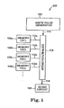
- FIG. 1 illustrates a block diagram of one embodiment of a memory device 100.
- Memory device 100 includes a write pulse generator 102, a distribution circuit 104, memory cells 106a, 106b, 106c, and 106d, and a sense circuit 108.
- memory cells 106a-106d are phase-change memory cells that are based on the amorphous to crystalline phase transition of the memory material.
- Write pulse generator 102 is electrically coupled to distribution circuit 104 through signal path 110.
- Distribution circuit 104 is electrically coupled to memory cells 106a-106d through signal paths 112a-112d, respectively, and to sense circuit 108 through signal path 114.
- Each phase-change memory cell 106a-106d includes phase-change material providing a storage location.
- the phase-change material of each phase-change memory cell includes three phase-change material portions.
- the composition of the phase-change material varies between adjacent phase-change material portions.
- the first phase-change material portion includes a first phase-change material composition and contacts a first electrode of the phase-change memory cell.
- the second phase-change material portion includes a second phase-change material composition and contacts a second electrode of the phase-change memory cell.
- the third phase-change material portion includes a third phase-change material composition and is between the first phase-change material portion and the second phase-change material portion.
- the first phase-change material portion thermally insulates the first electrode
- the second phase-change material portion thermally insulates the second electrode.
- the first phase-change material portion and the second phase-change material portion include the same phase-change material composition.
- the first phase-change material portion and the second phase-change material portion include different phase-change material compositions.
- the third phase-change material portion which is thermally insulated by the first phase-change material portion and the second phase-change material portion, provides the active region for the phase-change memory cell.
- the active region for the phase-change memory cell is where the phase-change material transitions between the crystalline state and the amorphous state for storing one bit, 1.5 bits, two bits, or several bits of data.
- write pulse generator 102 generates current or voltage pulses that are controllably directed to memory cells 106a-106d via distribution circuit 104.
- distribution circuit 104 includes a plurality of transistors that controllably direct current or voltage pulses to the memory cells.
- memory cells 106a-106d are made of a phase-change material that may be changed from an amorphous state to a crystalline state or from a crystalline state to an amorphous state under influence of temperature change.
- the degree of crystallinity thereby defines at least two memory states for storing data within memory device 100.
- the at least two memory states can be assigned to the bit values "0" and "1".
- the bit states of memory cells 106a-106d differ significantly in their electrical resistivity. In the amorphous state, a phase-change material exhibits significantly higher resistivity than in the crystalline state. In this way, sense amplifier 108 reads the cell resistance such that the bit value assigned to a particular memory cell 106a-106d is determined.
- write pulse generator 102 To program a memory cell 106a-106d within memory device 100, write pulse generator 102 generates a current or voltage pulse for heating the phase-change material in the target memory cell. In one embodiment, write pulse generator 102 generates an appropriate current or voltage pulse, which is fed into distribution circuit 104 and distributed to the appropriate target memory cell 106a-106d. The current or voltage pulse amplitude and duration is controlled depending on whether the memory cell is being set or reset. Generally, a "set” operation of a memory cell is heating the phase-change material of the target memory cell above its crystallization temperature (but below its melting temperature) long enough to achieve the crystalline state. Generally, a "reset” operation of a memory cell is heating the phase-change material of the target memory cell above its melting temperature, and then quickly quench cooling the material, thereby achieving the amorphous state.
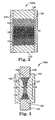
- Phase-change memory cell 120a includes a first electrode 122, phase-change material 134, a second electrode 130, and insulation material 132.
- Phase-change material 134 provides a storage location for storing one bit, 1.5 bits, two bits, or several bits of data.
- Phase-change material 134 is laterally completely enclosed by insulation material 132, which defines the current path and hence the location of the phase change region in phase-change material 134.
- each of the memory cells 106a-106d is similar to phase-change memory cell 120a.
- First electrode 122 is TiN, TaN, W, Al, Cu, TiSiN, TaSiN, or another suitable electrode material.
- Second electrode 130 is TiN, TaN, W, Al, Cu, TiSiN, TaSiN, or another suitable electrode material.
- Insulation material 132 is SiO 2 , fluorinated silica glass (FSG), doped boro-phosphorous silicate glass (BPSG), porous oxide, low-k dielectric, or another suitable dielectric material.
- Phase-change material 134 may be made up of a variety of materials in accordance with the present invention. Generally, chalcogenide alloys that contain one or more elements from group VI of the periodic table are useful as such materials.
- phase-change material 134 of memory cell 120a is made up of a chalcogenide compound material, such as GeSbTe, SbTe, GeTe, or AgInSbTe.
- the phase-change material can be chalcogen free, such as GeSb, GaSb, InSb, or GeGaInSb.
- the phase-change material can be made up of any suitable material including one or more of the elements Ge, Sb, Te, Ga, As, In, Se, and S.
- Phase-change material 134 may be selectively doped with nitrogen, oxygen, silicon, or another suitable material to modify the thermal conductivity, resistivity, and/or melting temperature of different portions of the phase-change material.
- Phase-change material 134 includes a first portion 124 in contact with first electrode 122, a second portion 128 in contact with second electrode 130, and a third portion 126 between first portion 124 and second portion 128.
- First portion 124 of phase-change material 134 includes a first phase-change material composition.
- Second portion 128 of phase-change material 134 includes a second phase-change material composition, and third portion 126 of phase-change material 134 includes a third phase-change material composition.
- the first phase-change material composition gradually transitions to the third phase-change material composition, and the third phase-change material composition gradually transitions to the second phase-change material composition.
- the phase-change material composition of first portion 124 includes the same phase-change material composition as second portion 128. In other embodiments, the phase-change material composition of first portion 124 is different from the phase-change material composition of second portion 128.
- phase-change material 134 is transitioned from the first phase-change material composition to the third phase-change material composition and from the third phase-change material composition to the second phase-change material composition by varying a doping level while depositing phase-change material 134.
- phase-change material 134 can comprise GeSbTe. While depositing the GeSbTe, a nitrogen flow, an oxygen flow, or another suitable dopant flow is gradually increased to transition the phase-change material composition of first portion 124 from undoped GeSbTe contacting first electrode 122 to a doped GeSbTe of third portion 126. The doping level varies continuously from first portion 124 to second portion 128. At the center of third portion 126, the doping level is gradually decreased to transition the doped GeSbTe of third portion 126 to undoped GeSbTe of second portion 128 contacting second electrode 130.
- First portion 124 and second portion 128 of phase-change material 134 have a lower resistivity and preferably have a lower thermal conductivity and a higher melting temperature than third portion 126 of phase-change material 134 due to the doping level. Therefore, first portion 124 and second portion 128 thermally insulate first electrode 122 and second electrode 130, respectively, such that the active phase-change region is confined to third portion 126.
- the doping level By adjusting the doping level, the size of first portion 124, second portion 128, and third portion 126 can be adjusted to achieve a desired size for the active region. Also, by adjusting the doping levels within each portion 124, 126, and 128 of phase-change material 134, phase-change memory cell 120a can be optimized for multi-bit data storage.
- phase-change memory cell 120a During operation of phase-change memory cell 120a, a write pulse is applied between first electrode 122 and second electrode 130 to program phase-change memory cell 120a. Since first portion 124 and second portion 128 of phase-change material 134 insulate third portion 126 of phase-change material 134, the highest temperature within phase-change material 134 during a write pulse is within third portion 126. In addition, due to the higher resistivity of third portion 126, more heat is generated within third portion 126 than within first portion 124 and second portion 128.
- phase-change memory cell 120a During a set operation of phase-change memory cell 120a, a set current or voltage pulse is selectively enabled to the selection device and sent through first electrode 122 to phase-change material 134 thereby heating third portion 126 of phase-change material 134 above its crystallization temperature (but usually below its melting temperature). In this way, third portion 126 of phase-change material 134 reaches its crystalline state during this set operation.
- a reset current or voltage pulse is selectively enabled to the selection device and sent through first electrode 122 to phase-change material 134. The reset current or voltage quickly heats third portion 126 of phase-change material 134 above its melting temperature. After the current or voltage pulse is turned off, third portion 126 of phase-change material 134 quickly quench cools into the amorphous state.
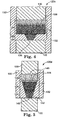
- Phase-change memory cell 120b is a pillar phase-change memory cell.
- Phase-change memory cell 120b includes first electrode 122, phase-change material 134, second electrode 130, and insulation material 132.
- Phase-change material 134 provides a storage location for storing one bit, 1.5 bits, two bits, or several bits of data.
- Phase-change material 134 is laterally completely enclosed by insulation material 132, which defines the current path and hence the location of the phase change region in phase-change material 134.
- each of the memory cells 106a-106d is similar to phase-change memory cell 120b.
- Phase-change material 134 includes a first portion 124 in contact with first electrode 122 at 125, a second portion 128 in contact with second electrode 130 at 129, and a third portion 126 between first portion 124 and second portion 128.
- First portion 124 of phase-change material 134 has a maximum width or cross-section at 125
- second portion 128 of phase-change material 134 has a maximum width or cross-section at 129
- third portion 126 of phase-change material 134 has a minimum width or cross-section at 127.
- the maximum width at 125 of first portion 124 and the maximum width at 129 of second portion 128 are greater than the minimum width at 127 of third portion 126.
- a maximum width of third portion 126 is less than a minimum width of first portion 124 and a minimum width of second portion 128. In another embodiment, a maximum width of third portion 126 is less than a maximum width of first portion 124 and a maximum width of second portion 128. In another embodiment, a minimum width of third portion 126 is less than a minimum width of first portion 124 and a minimum width of second portion 128. In one embodiment, the maximum width at 125 of first portion 124 is approximately equal to the maximum width at 129 of second portion 128. In other embodiments, the maximum width at 125 of first portion 124 is different than the maximum width at 129 of second portion 128. In one embodiment, phase-change material 134 forms an hourglass shape.
- Portions 124, 126, and 128 of phase-change material 134 of phase-change memory cell 120b have similar phase-change material compositions and functions as the corresponding portions 124, 126, and 128 of phase-change memory cell 120a previously described and illustrated with reference to Figure 2.
- Phase-change memory cell 120b operates similarly to phase-change memory cell 120a.
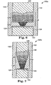
- Phase-change memory cell 120c is a tapered via phase-change memory cell.
- Phase-change memory cell 120c includes first electrode 122, phase-change material 134, second electrode 130, and insulation material 132.
- Phase-change material 134 provides a storage location for storing one bit, 1.5 bits, two bits, or several bits of data.
- Phase-change material 134 is laterally completely enclosed by insulation material 132, which defines the current path and hence the location of the phase change region in phase-change material 134.
- each of the memory cells 106a-106d is similar to phase-change memory cell 120c.
- Phase-change material 134 includes a first portion 124 in contact with first electrode 122 at 138, a second portion 128 in contact with second electrode 130, and a third portion 126 between first portion 124 and second portion 128.
- First portion 124 and third portion 126 of phase-change material 134 have tapered sidewalls and has a maximum width or cross-section at 136 and a minimum width or cross-section at 138.
- first portion 124 and third portion 126 may extend up the sides of second portion 128 due to sidewall covering during the deposition of first portion 124 and third portion 126 of phase-change material 134.
- Portions 124, 126, and 128 of phase-change material 134 of phase-change memory cell 120c have similar phase-change material compositions and functions as the corresponding portions 124, 126, and 128 of phase-change memory cell 120a previously described and illustrated with reference to Figure 2.
- Phase-change memory cell 120c operates similarly to phase-change memory cell 120a.
- Phase-change memory cell 120d is a tapered via phase-change memory cell.
- Phase-change memory cell 120d includes first electrode 122, phase-change material 134, second electrode 130, and insulation material 132.
- Phase-change material 134 provides a storage location for storing one bit, 1.5 bits, two bits, or several bits of data.
- Phase-change material 134 is laterally completely enclosed by insulation material 132, which defines the current path and hence the location of the phase-change region in phase-change material 134.
- each of the memory cells 106a-106d is similar to phase-change memory cell 120d.
- Phase-change material 134 includes a first portion 124 in contact with first electrode 122 at 140, a second portion 128 in contact with second electrode 130 at 146, and a third portion 126 between first portion 124 and second portion 128.
- First portion 124 of phase-change material 134 has a maximum width or cross-section at 142 and a minimum width or cross-section at 140.
- Second portion 128 of phase-change material 134 has a maximum width or cross-section at 146 and a minimum width or cross-section at 144.
- Third portion 126 of phase-change material 134 has a maximum width or cross-section at 144 and a minimum width or cross-section at 142.
- first portion 124 and third portion 126 may extend up the sides of second portion 128 due to sidewall covering during the deposition of first portion 124 and third portion 126 of phase-change material 134.
- a minimum width of first portion 124 is less than a minimum width of third portion 126. In another embodiment, a maximum width of first portion 124 is less than a minimum width of third portion 126. In another embodiment, a maximum width of first portion 124 is less than a maximum width of third portion 126. In one embodiment, a minimum width of third portion 126 is less than a minimum width of second portion 128. In another embodiment, a maximum width of third portion 126 is less than a minimum width of second portion 128. In another embodiment, a maximum width of third portion 126 is less than a maximum width of second portion 128. In one embodiment, phase-change material 134 has tapered sidewalls.
- Portions 124, 126, and 128 of phase-change material 134 of phase-change memory cell 120d have similar phase-change material compositions and functions as the corresponding portions 124, 126, and 128 of phase-change memory cell 120a previously described and illustrated with reference to Figure 2.
- Phase-change memory cell 120d operates similarly to phase-change memory cell 120a.
- Phase-change memory cell 150a is a tapered via phase-change memory cell.
- Phase-change memory cell 150a includes first electrode 122, phase-change material 134, second electrode 130, and insulation material 132.
- Phase-change material 134 provides a storage location for storing one bit, 1.5 bits, two bits, or several bits of data.
- Phase-change material 134 is laterally completely enclosed by insulation material 132, which defines the current path and hence the location of the phase change region in phase-change material 134.
- each of the memory cells 106a-106d is similar to phase-change memory cell 150a.
- Phase-change material 134 includes a first portion 124 in contact with first electrode 122, a second portion 128 in contact with second electrode 130, and a third portion 126 contacting first portion 124 at 138 and second portion 128.
- First portion 124 of phase-change material 134 has a width or cross-section equal to the width or cross-section of first electrode 122.
- Third portion 126 of phase-change material 134 has tapered sidewalls and has a maximum width or cross-section at 136 and a minimum width or cross-section at 138. In other embodiments, third portion 126 may extend up the sides of second portion 128 due to sidewall covering during the deposition of third portion 126 of phase-change material 134.
- First portion 124 of phase-change material 134 includes a first phase-change material composition.
- Second portion 128 of phase-change material 134 includes a second phase-change material composition, and third portion 126 of phase-change material 134 includes a third phase-change material composition.
- the first phase-change material composition is constant, and the third phase-change material composition gradually transitions to the second phase-change material composition.
- the phase-change material composition of first portion 124 includes the same phase-change material composition as second portion 128. In other embodiments, the phase-change material composition of first portion 124 is different from the phase-change material composition of second portion 128.
- phase-change material 134 is transitioned from the third phase-change material composition to the second phase-change material composition by varying a doping level while depositing phase-change material 134.
- phase-change material 134 can comprise GeSbTe. While depositing the GeSbTe, a nitrogen flow, an oxygen flow, or another suitable dopant flow is gradually decreased to transition the phase-change material composition of third portion 126 from doped GeSbTe contacting first portion 124 at 138 to undoped GeSbTe of second portion 128.
- the doping level varies continuously from third portion 126 to second portion 128, such that undoped GeSbTe of second portion 128 contacts second electrode 130.
- First portion 124 and second portion 128 of phase-change material 134 have a lower resistivity and preferably have a lower thermal conductivity and a higher melting temperature than third portion 126 of phase-change material 134 due to the doping level. Therefore, first portion 124 and second portion 128 thermally insulate first electrode 122 and second electrode 130, respectively, such that the active phase-change region is confined to third portion 126.
- the doping level By adjusting the doping level, the size of second portion 128 and third portion 126 can be adjusted to achieve a desired size for the active region. Also, by adjusting the doping levels within each portion 126 and 128, phase-change memory cell 150a can be optimized for multi-bit data storage.
- phase-change memory cell 150a During operation of phase-change memory cell 150a, a write pulse is applied between first electrode 122 and second electrode 130 to program phase-change memory cell 150a. Since first portion 124 and second portion 128 of phase-change material 134 have a lower thermal conductivity than third portion 126 of phase-change material 134, the highest temperature within phase-change material 134 during a write pulse is within third portion 126. Phase-change memory cell 150a operates similarly to phase-change memory cell 120a.
- Phase-change memory cell 150b is a tapered via phase-change memory cell.
- Phase-change memory cell 150b includes first electrode 122, phase-change material 134, second electrode 130, and insulation material 132.
- Phase-change material 134 provides a storage location for storing one bit, 1.5 bits, two bits, or several bits of data.
- Phase-change material 134 is laterally completely enclosed by insulation material 132, which defines the current path and hence the location of the phase-change region in phase-change material 134.
- each of the memory cells 106a-106d is similar to phase-change memory cell 150b.
- Phase-change material 134 includes a first portion 124 in contact with first electrode 122, a second portion 128 in contact with second electrode 130 at 146, and a third portion 126 contacting first portion 124 at 140 and second portion 128.
- First portion 124 of phase-change material 134 has the same width or cross-section as first electrode 122.
- Second portion 128 of phase-change material 134 has a maximum width or cross-section at 146 and a minimum width or cross-section at 144.
- Third portion 126 of phase-change material 134 has a maximum width or cross-section at 144 and a minimum width or cross-section at 140.
- third portion 126 may extend up the sides of second portion 128 due to sidewall covering during the deposition of third portion 126 of phase-change material 134.
- a minimum width of third portion 126 is less than a minimum width of second portion 128. In another embodiment, a maximum width of third portion 126 is less than a minimum width of second portion 128. In another embodiment, a maximum width of third portion 126 is less than a maximum width of second portion 128. In one embodiment, second portion 128 and third portion 126 of phase-change material 134 have tapered sidewalls.
- Phase-change memory cell 150b operates similarly to phase-change memory cell 120a.
- Phase-change memory cell 160a is a tapered via phase-change memory cell.
- Phase-change memory cell 160a includes first electrode 122, phase-change material 134, second electrode 130, and insulation material 132.
- Phase-change material 134 provides a storage location for storing one bit, 1.5 bits, two bits, or several bits of data.
- Phase-change material 134 is laterally completely enclosed by insulation material 132, which defines the current path and hence the location of the phase change region in phase-change material 134.
- each of the memory cells 106a-106d is similar to phase-change memory cell 160a.
- Phase-change material 134 includes a first portion 124 in contact with first electrode 122, a second portion 128 in contact with second electrode 130, and a third portion 126 contacting first portion 124 at 138 and second portion 128.
- First portion 124 of phase-change material 134 has a width or cross-section equal to the width or cross-section of first electrode 122.
- Third portion 126 of phase-change material 134 laterally completely surrounds second portion 128 of phase-change material 134.
- the lower part 127 of second portion 128 of phase-change material 134 has tapered sidewalls and has a maximum width or cross-section at 136 and a minimum width or cross-section near 138.
- First portion 124 of phase-change material 134 includes a first phase-change material composition.
- Second portion 128 of phase-change material 134 includes a second phase-change material composition, and third portion 126 of phase-change material 134 includes a third phase-change material composition.
- the first, second, and third phase-change material compositions are constant.
- the phase-change material composition of first portion 124 includes the same phase-change material composition as second portion 128. In other embodiments, the phase-change material composition of first portion 124 is different from the phase-change material composition of second portion 128.
- First portion 124 and second portion 128 of phase-change material 134 have a lower resistivity and preferably have a lower thermal conductivity and a higher melting temperature than third portion 126 of phase-change material 134 due to the phase-change materials selected. Therefore, first portion 124 and second portion 128 thermally insulate first electrode 122 and second electrode 130, respectively, such that the active phase-change region is confined to third portion 126. In particular, the active phase-change region is confined to the phase-change material between first portion 124 at 138 and the lower part 127 of second portion 128.
- the amount of phase-change material deposited for third portion 126 the size of second portion 128 and third portion 126 can be adjusted to achieve a desired size for the active region. Also, by adjusting the amount and type of phase-change material deposited for third portion 126, phase-change memory cell 160a can be optimized for multi-bit data storage.
- phase-change memory cell 160a During operation of phase-change memory cell 160a, a write pulse is applied between first electrode 122 and second electrode 130 to program phase-change memory cell 160a. Since first portion 124 and second portion 128 of phase-change material 134 insulate third portion 126 of phase-change material 134, the highest temperature within phase-change material 134 during a write pulse is within third portion 126. In addition, due to the higher resistivity of third portion 126, more heat is generated within third portion 126 than within first portion 124 and second portion 128. Phase-change memory cell 160a operates similarly to phase-change memory cell 120a.
- phase-change memory cell 160b is a tapered via phase-change memory cell.
- Phase-change memory cell 160b includes first electrode 122, phase-change material 134, second electrode 130, and insulation material 132.
- Phase-change material 134 provides a storage location for storing one bit, 1.5 bits, two bits, or several bits of data.
- Phase-change material 134 is laterally completely enclosed by insulation material 132, which defines the current path and hence the location of the phase change region in phase-change material 134.
- each of the memory cells 106a-106d is similar to phase-change memory cell 160b.
- Phase-change material 134 includes a first portion 124 in contact with first electrode 122, a second portion 128 in contact with second electrode 130 at 146, and a third portion 126 contacting first portion 124 at 140 and second portion 128.
- First portion 124 of phase-change material 134 has the same width or cross-section as first electrode 122.
- Second portion 128 of phase-change material 134 has a maximum width or cross-section at 146 and a minimum width or cross-section at 148.
- Third portion 126 of phase-change material 134 laterally completely surrounds second portion 128 of phase-change material 134.
- second portion 128 of phase-change material 134 has tapered sidewalls.
- Phase-change memory cell 160b operates similarly to phase-change memory cell 120a.
- Phase-change memory cell 170 is a bridge phase-change memory cell.
- Phase-change memory cell 170 includes first electrode 122, a first contact 172, phase-change material 134, a second contact 176, a spacer 174, second electrode 130, and dielectric material 132.
- Phase-change material 134 provides a storage location for storing one bit, 1.5 bits, two bits, or several bits of data.
- Phase-change material 134 includes a first portion 124 in contact with first contact 172 and a second portion 128 in contact with second contact 176 separated by spacer 174.
- First contact 172 contacts first electrode 122 and second contact 176 contacts second electrode 130.
- First portion 124 of phase-change material 134 includes a first phase-change material composition.
- Second portion 128 of phase-change material 134 includes a second phase-change material composition.
- First portion 124 of phase-change material 134 has a lower resistivity and preferably has a lower thermal conductivity and a higher melting temperature than second portion 128 of phase-change material 134 due to the phase-change materials selected. Therefore, first portion 124 thermally insulates first contact 172, such that the active phase-change region is confined to second portion 128.
- phase-change memory cell 170 can be optimized for multi-bit data storage.
- phase-change memory cell 170 During operation of phase-change memory cell 170, a write pulse is applied between first contact 171 and second contact 176 to program phase-change memory cell 170. Since first portion 124 insulates second portion 128 of phase-change material 134, the highest temperature within phase-change material 134 during a write pulse is within second portion 128. In addition, due to the higher resistivity of second portion 128, more heat is generated within second portion 128 than within first portion 124. Phase-change memory cell 170 operates similarly to phase-change memory cell 120a.
- Embodiments of the present invention provide a phase-change memory cell including phase-change material having three portions.
- the first portion of the phase-change material insulates the first electrode, and the second portion of the phase-change material insulates the second electrode.
- the third portion of the phase-change material which is insulated by the first portion and the third portion, is the active region.
Abstract
Description
- This application is related to
U.S. Patent Application Serial Number 11/187,533 - Phase-change memories include phase-change materials that exhibit at least two different states. Phase-change material may be used in memory cells to store bits of data. The states of phase-change material may be referenced to as amorphous and crystalline states. The states may be distinguished because the amorphous state generally exhibits higher resistivity than does the crystalline state. Generally, the amorphous state involves a more disordered atomic structure, while the crystalline state is an ordered lattice. Some phase-change materials exhibit two crystalline states, e.g. a face-centered cubic (FCC) state and a hexagonal closest packing (HCP) state. These two crystalline states have different resistivities and may be used to store bits of data. In the following description, the amorphous state generally refers to the state having the higher resistivity, and the crystalline state generally refers to the state having the lower resistivity.
- Phase change in the phase-change materials may be induced reversibly. In this way, the memory may change from the amorphous state to the crystalline state, and from the crystalline state to the amorphous state, in response to temperature changes. The temperature changes to the phase-change material may be achieved in a variety of ways. For example, a laser can be directed to the phase-change material, current may be driven through the phase-change material, or current can be fed through a resistive heater adjacent the phase-change material. With any of these methods, controllable heating of the phase-change material causes controllable phase change within the phase-change material.
- When a phase-change memory comprises a memory array having a plurality of memory cells that are made of phase-change material, the memory may be programmed to store data utilizing the memory states of the phase-change material. One way to read and write data in such a phase-change memory device is to control a current and/or a voltage pulse that is applied to the phase-change material. The level of current and voltage generally corresponds to the temperature induced within the phase-change material in each memory cell.
- One embodiment of the present invention provides a memory cell. The memory cell includes a first electrode, a second electrode, and a first portion of phase-change material contacting the first electrode. The memory cell includes a second portion of phase-change material contacting the second electrode and a third portion of phase-change material between the first portion and the second portion. A phase-change material composition of the third portion and the second portion gradually transitions from the third portion to the second portion.
- The accompanying drawings are included to provide a further understanding of the present invention and are incorporated in and constitute a part of this specification. The drawings illustrate the embodiments of the present invention and together with the description serve to explain the principles of the invention. Other embodiments of the present invention and many of the intended advantages of the present invention will be readily appreciated as they become better understood by reference to the following detailed description. The elements of the drawings are not necessarily to scale relative to each other. Like reference numerals designate corresponding similar parts.
- Figure 1 illustrates a block diagram of one embodiment of a memory device.
- Figure 2 illustrates a cross-sectional view of one embodiment of a phase-change memory cell.
- Figure 3 illustrates a cross-sectional view of another embodiment of a phase-change memory cell.
- Figure 4 illustrates a cross-sectional view of another embodiment of a phase-change memory cell.
- Figure 5 illustrates a cross-sectional view of another embodiment of a phase-change memory cell.
- Figure 6 illustrates a cross-sectional view of another embodiment of a phase-change memory cell.
- Figure 7 illustrates a cross-sectional view of another embodiment of a phase-change memory cell.
- Figure 8 illustrates a cross-sectional view of another embodiment of a phase-change memory cell.
- Figure 9 illustrates a cross-sectional view of another embodiment of a phase-change memory cell.
- Figure 10 illustrates a cross-sectional view of another embodiment of a phase-change memory cell.
- Figure 1 illustrates a block diagram of one embodiment of a
memory device 100.Memory device 100 includes awrite pulse generator 102, adistribution circuit 104,memory cells sense circuit 108. In one embodiment,memory cells 106a-106d are phase-change memory cells that are based on the amorphous to crystalline phase transition of the memory material.Write pulse generator 102 is electrically coupled todistribution circuit 104 throughsignal path 110.Distribution circuit 104 is electrically coupled tomemory cells 106a-106d throughsignal paths 112a-112d, respectively, and to sensecircuit 108 throughsignal path 114. - Each phase-
change memory cell 106a-106d includes phase-change material providing a storage location. The phase-change material of each phase-change memory cell includes three phase-change material portions. The composition of the phase-change material varies between adjacent phase-change material portions. The first phase-change material portion includes a first phase-change material composition and contacts a first electrode of the phase-change memory cell. The second phase-change material portion includes a second phase-change material composition and contacts a second electrode of the phase-change memory cell. The third phase-change material portion includes a third phase-change material composition and is between the first phase-change material portion and the second phase-change material portion. - The first phase-change material portion thermally insulates the first electrode, and the second phase-change material portion thermally insulates the second electrode. In one embodiment, the first phase-change material portion and the second phase-change material portion include the same phase-change material composition. In other embodiments, the first phase-change material portion and the second phase-change material portion include different phase-change material compositions. The third phase-change material portion, which is thermally insulated by the first phase-change material portion and the second phase-change material portion, provides the active region for the phase-change memory cell. The active region for the phase-change memory cell is where the phase-change material transitions between the crystalline state and the amorphous state for storing one bit, 1.5 bits, two bits, or several bits of data.
- In one embodiment, write
pulse generator 102 generates current or voltage pulses that are controllably directed tomemory cells 106a-106d viadistribution circuit 104. In one embodiment,distribution circuit 104 includes a plurality of transistors that controllably direct current or voltage pulses to the memory cells. - In one embodiment,
memory cells 106a-106d are made of a phase-change material that may be changed from an amorphous state to a crystalline state or from a crystalline state to an amorphous state under influence of temperature change. The degree of crystallinity thereby defines at least two memory states for storing data withinmemory device 100. The at least two memory states can be assigned to the bit values "0" and "1". The bit states ofmemory cells 106a-106d differ significantly in their electrical resistivity. In the amorphous state, a phase-change material exhibits significantly higher resistivity than in the crystalline state. In this way,sense amplifier 108 reads the cell resistance such that the bit value assigned to aparticular memory cell 106a-106d is determined. - To program a
memory cell 106a-106d withinmemory device 100, writepulse generator 102 generates a current or voltage pulse for heating the phase-change material in the target memory cell. In one embodiment, writepulse generator 102 generates an appropriate current or voltage pulse, which is fed intodistribution circuit 104 and distributed to the appropriatetarget memory cell 106a-106d. The current or voltage pulse amplitude and duration is controlled depending on whether the memory cell is being set or reset. Generally, a "set" operation of a memory cell is heating the phase-change material of the target memory cell above its crystallization temperature (but below its melting temperature) long enough to achieve the crystalline state. Generally, a "reset" operation of a memory cell is heating the phase-change material of the target memory cell above its melting temperature, and then quickly quench cooling the material, thereby achieving the amorphous state. - Figure 2 illustrates a cross-sectional view of one embodiment of a phase-
change memory cell 120a. Phase-change memory cell 120a includes afirst electrode 122, phase-change material 134, asecond electrode 130, andinsulation material 132. Phase-change material 134 provides a storage location for storing one bit, 1.5 bits, two bits, or several bits of data. Phase-change material 134 is laterally completely enclosed byinsulation material 132, which defines the current path and hence the location of the phase change region in phase-change material 134. In one embodiment, each of thememory cells 106a-106d is similar to phase-change memory cell 120a. -
First electrode 122 is TiN, TaN, W, Al, Cu, TiSiN, TaSiN, or another suitable electrode material.Second electrode 130 is TiN, TaN, W, Al, Cu, TiSiN, TaSiN, or another suitable electrode material.Insulation material 132 is SiO2, fluorinated silica glass (FSG), doped boro-phosphorous silicate glass (BPSG), porous oxide, low-k dielectric, or another suitable dielectric material. - Phase-
change material 134 may be made up of a variety of materials in accordance with the present invention. Generally, chalcogenide alloys that contain one or more elements from group VI of the periodic table are useful as such materials. In one embodiment, phase-change material 134 ofmemory cell 120a is made up of a chalcogenide compound material, such as GeSbTe, SbTe, GeTe, or AgInSbTe. In another embodiment, the phase-change material can be chalcogen free, such as GeSb, GaSb, InSb, or GeGaInSb. In other embodiments, the phase-change material can be made up of any suitable material including one or more of the elements Ge, Sb, Te, Ga, As, In, Se, and S. Phase-change material 134 may be selectively doped with nitrogen, oxygen, silicon, or another suitable material to modify the thermal conductivity, resistivity, and/or melting temperature of different portions of the phase-change material. - Phase-
change material 134 includes afirst portion 124 in contact withfirst electrode 122, asecond portion 128 in contact withsecond electrode 130, and athird portion 126 betweenfirst portion 124 andsecond portion 128.First portion 124 of phase-change material 134 includes a first phase-change material composition.Second portion 128 of phase-change material 134 includes a second phase-change material composition, andthird portion 126 of phase-change material 134 includes a third phase-change material composition. The first phase-change material composition gradually transitions to the third phase-change material composition, and the third phase-change material composition gradually transitions to the second phase-change material composition. In one embodiment, the phase-change material composition offirst portion 124 includes the same phase-change material composition assecond portion 128. In other embodiments, the phase-change material composition offirst portion 124 is different from the phase-change material composition ofsecond portion 128. - In one embodiment, phase-
change material 134 is transitioned from the first phase-change material composition to the third phase-change material composition and from the third phase-change material composition to the second phase-change material composition by varying a doping level while depositing phase-change material 134. For example, phase-change material 134 can comprise GeSbTe. While depositing the GeSbTe, a nitrogen flow, an oxygen flow, or another suitable dopant flow is gradually increased to transition the phase-change material composition offirst portion 124 from undoped GeSbTe contactingfirst electrode 122 to a doped GeSbTe ofthird portion 126. The doping level varies continuously fromfirst portion 124 tosecond portion 128. At the center ofthird portion 126, the doping level is gradually decreased to transition the doped GeSbTe ofthird portion 126 to undoped GeSbTe ofsecond portion 128 contactingsecond electrode 130. -
First portion 124 andsecond portion 128 of phase-change material 134 have a lower resistivity and preferably have a lower thermal conductivity and a higher melting temperature thanthird portion 126 of phase-change material 134 due to the doping level. Therefore,first portion 124 andsecond portion 128 thermally insulatefirst electrode 122 andsecond electrode 130, respectively, such that the active phase-change region is confined tothird portion 126. By adjusting the doping level, the size offirst portion 124,second portion 128, andthird portion 126 can be adjusted to achieve a desired size for the active region. Also, by adjusting the doping levels within eachportion change material 134, phase-change memory cell 120a can be optimized for multi-bit data storage. - During operation of phase-
change memory cell 120a, a write pulse is applied betweenfirst electrode 122 andsecond electrode 130 to program phase-change memory cell 120a. Sincefirst portion 124 andsecond portion 128 of phase-change material 134 insulatethird portion 126 of phase-change material 134, the highest temperature within phase-change material 134 during a write pulse is withinthird portion 126. In addition, due to the higher resistivity ofthird portion 126, more heat is generated withinthird portion 126 than withinfirst portion 124 andsecond portion 128. - During a set operation of phase-
change memory cell 120a, a set current or voltage pulse is selectively enabled to the selection device and sent throughfirst electrode 122 to phase-change material 134 thereby heatingthird portion 126 of phase-change material 134 above its crystallization temperature (but usually below its melting temperature). In this way,third portion 126 of phase-change material 134 reaches its crystalline state during this set operation. During a reset operation of phase-change memory cell 120a, a reset current or voltage pulse is selectively enabled to the selection device and sent throughfirst electrode 122 to phase-change material 134. The reset current or voltage quickly heatsthird portion 126 of phase-change material 134 above its melting temperature. After the current or voltage pulse is turned off,third portion 126 of phase-change material 134 quickly quench cools into the amorphous state. - Figure 3 illustrates a cross-sectional view of another embodiment of a phase-
change memory cell 120b. In one embodiment, phase-change memory cell 120b is a pillar phase-change memory cell. Phase-change memory cell 120b includesfirst electrode 122, phase-change material 134,second electrode 130, andinsulation material 132. Phase-change material 134 provides a storage location for storing one bit, 1.5 bits, two bits, or several bits of data. Phase-change material 134 is laterally completely enclosed byinsulation material 132, which defines the current path and hence the location of the phase change region in phase-change material 134. In one embodiment, each of thememory cells 106a-106d is similar to phase-change memory cell 120b. - Phase-
change material 134 includes afirst portion 124 in contact withfirst electrode 122 at 125, asecond portion 128 in contact withsecond electrode 130 at 129, and athird portion 126 betweenfirst portion 124 andsecond portion 128.First portion 124 of phase-change material 134 has a maximum width or cross-section at 125,second portion 128 of phase-change material 134 has a maximum width or cross-section at 129, andthird portion 126 of phase-change material 134 has a minimum width or cross-section at 127. The maximum width at 125 offirst portion 124 and the maximum width at 129 ofsecond portion 128 are greater than the minimum width at 127 ofthird portion 126. - In one embodiment, a maximum width of
third portion 126 is less than a minimum width offirst portion 124 and a minimum width ofsecond portion 128. In another embodiment, a maximum width ofthird portion 126 is less than a maximum width offirst portion 124 and a maximum width ofsecond portion 128. In another embodiment, a minimum width ofthird portion 126 is less than a minimum width offirst portion 124 and a minimum width ofsecond portion 128. In one embodiment, the maximum width at 125 offirst portion 124 is approximately equal to the maximum width at 129 ofsecond portion 128. In other embodiments, the maximum width at 125 offirst portion 124 is different than the maximum width at 129 ofsecond portion 128. In one embodiment, phase-change material 134 forms an hourglass shape. -
Portions change material 134 of phase-change memory cell 120b have similar phase-change material compositions and functions as the correspondingportions change memory cell 120a previously described and illustrated with reference to Figure 2. Phase-change memory cell 120b operates similarly to phase-change memory cell 120a. - Figure 4 illustrates a cross-sectional view of another embodiment of a phase-
change memory cell 120c. In one embodiment, phase-change memory cell 120c is a tapered via phase-change memory cell. Phase-change memory cell 120c includesfirst electrode 122, phase-change material 134,second electrode 130, andinsulation material 132. Phase-change material 134 provides a storage location for storing one bit, 1.5 bits, two bits, or several bits of data. Phase-change material 134 is laterally completely enclosed byinsulation material 132, which defines the current path and hence the location of the phase change region in phase-change material 134. In one embodiment, each of thememory cells 106a-106d is similar to phase-change memory cell 120c. - Phase-
change material 134 includes afirst portion 124 in contact withfirst electrode 122 at 138, asecond portion 128 in contact withsecond electrode 130, and athird portion 126 betweenfirst portion 124 andsecond portion 128.First portion 124 andthird portion 126 of phase-change material 134 have tapered sidewalls and has a maximum width or cross-section at 136 and a minimum width or cross-section at 138. In other embodiments,first portion 124 andthird portion 126 may extend up the sides ofsecond portion 128 due to sidewall covering during the deposition offirst portion 124 andthird portion 126 of phase-change material 134. -
Portions change material 134 of phase-change memory cell 120c have similar phase-change material compositions and functions as the correspondingportions change memory cell 120a previously described and illustrated with reference to Figure 2. Phase-change memory cell 120c operates similarly to phase-change memory cell 120a. - Figure 5 illustrates a cross-sectional view of another embodiment of a phase-
change memory cell 120d. In one embodiment, phase-change memory cell 120d is a tapered via phase-change memory cell. Phase-change memory cell 120d includesfirst electrode 122, phase-change material 134,second electrode 130, andinsulation material 132. Phase-change material 134 provides a storage location for storing one bit, 1.5 bits, two bits, or several bits of data. Phase-change material 134 is laterally completely enclosed byinsulation material 132, which defines the current path and hence the location of the phase-change region in phase-change material 134. In one embodiment, each of thememory cells 106a-106d is similar to phase-change memory cell 120d. - Phase-
change material 134 includes afirst portion 124 in contact withfirst electrode 122 at 140, asecond portion 128 in contact withsecond electrode 130 at 146, and athird portion 126 betweenfirst portion 124 andsecond portion 128.First portion 124 of phase-change material 134 has a maximum width or cross-section at 142 and a minimum width or cross-section at 140.Second portion 128 of phase-change material 134 has a maximum width or cross-section at 146 and a minimum width or cross-section at 144.Third portion 126 of phase-change material 134 has a maximum width or cross-section at 144 and a minimum width or cross-section at 142. In other embodiments,first portion 124 andthird portion 126 may extend up the sides ofsecond portion 128 due to sidewall covering during the deposition offirst portion 124 andthird portion 126 of phase-change material 134. - In one embodiment, a minimum width of
first portion 124 is less than a minimum width ofthird portion 126. In another embodiment, a maximum width offirst portion 124 is less than a minimum width ofthird portion 126. In another embodiment, a maximum width offirst portion 124 is less than a maximum width ofthird portion 126. In one embodiment, a minimum width ofthird portion 126 is less than a minimum width ofsecond portion 128. In another embodiment, a maximum width ofthird portion 126 is less than a minimum width ofsecond portion 128. In another embodiment, a maximum width ofthird portion 126 is less than a maximum width ofsecond portion 128. In one embodiment, phase-change material 134 has tapered sidewalls. -
Portions change material 134 of phase-change memory cell 120d have similar phase-change material compositions and functions as the correspondingportions change memory cell 120a previously described and illustrated with reference to Figure 2. Phase-change memory cell 120d operates similarly to phase-change memory cell 120a. - Figure 6 illustrates a cross-sectional view of another embodiment of a phase-
change memory cell 150a. In one embodiment, phase-change memory cell 150a is a tapered via phase-change memory cell. Phase-change memory cell 150a includesfirst electrode 122, phase-change material 134,second electrode 130, andinsulation material 132. Phase-change material 134 provides a storage location for storing one bit, 1.5 bits, two bits, or several bits of data. Phase-change material 134 is laterally completely enclosed byinsulation material 132, which defines the current path and hence the location of the phase change region in phase-change material 134. In one embodiment, each of thememory cells 106a-106d is similar to phase-change memory cell 150a. - Phase-
change material 134 includes afirst portion 124 in contact withfirst electrode 122, asecond portion 128 in contact withsecond electrode 130, and athird portion 126 contactingfirst portion 124 at 138 andsecond portion 128.First portion 124 of phase-change material 134 has a width or cross-section equal to the width or cross-section offirst electrode 122.Third portion 126 of phase-change material 134 has tapered sidewalls and has a maximum width or cross-section at 136 and a minimum width or cross-section at 138. In other embodiments,third portion 126 may extend up the sides ofsecond portion 128 due to sidewall covering during the deposition ofthird portion 126 of phase-change material 134. -
First portion 124 of phase-change material 134 includes a first phase-change material composition.Second portion 128 of phase-change material 134 includes a second phase-change material composition, andthird portion 126 of phase-change material 134 includes a third phase-change material composition. The first phase-change material composition is constant, and the third phase-change material composition gradually transitions to the second phase-change material composition. In one embodiment, the phase-change material composition offirst portion 124 includes the same phase-change material composition assecond portion 128. In other embodiments, the phase-change material composition offirst portion 124 is different from the phase-change material composition ofsecond portion 128. - In one embodiment, phase-
change material 134 is transitioned from the third phase-change material composition to the second phase-change material composition by varying a doping level while depositing phase-change material 134. For example, phase-change material 134 can comprise GeSbTe. While depositing the GeSbTe, a nitrogen flow, an oxygen flow, or another suitable dopant flow is gradually decreased to transition the phase-change material composition ofthird portion 126 from doped GeSbTe contactingfirst portion 124 at 138 to undoped GeSbTe ofsecond portion 128. The doping level varies continuously fromthird portion 126 tosecond portion 128, such that undoped GeSbTe ofsecond portion 128 contactssecond electrode 130. -
First portion 124 andsecond portion 128 of phase-change material 134 have a lower resistivity and preferably have a lower thermal conductivity and a higher melting temperature thanthird portion 126 of phase-change material 134 due to the doping level. Therefore,first portion 124 andsecond portion 128 thermally insulatefirst electrode 122 andsecond electrode 130, respectively, such that the active phase-change region is confined tothird portion 126. By adjusting the doping level, the size ofsecond portion 128 andthird portion 126 can be adjusted to achieve a desired size for the active region. Also, by adjusting the doping levels within eachportion change memory cell 150a can be optimized for multi-bit data storage. - During operation of phase-
change memory cell 150a, a write pulse is applied betweenfirst electrode 122 andsecond electrode 130 to program phase-change memory cell 150a. Sincefirst portion 124 andsecond portion 128 of phase-change material 134 have a lower thermal conductivity thanthird portion 126 of phase-change material 134, the highest temperature within phase-change material 134 during a write pulse is withinthird portion 126. Phase-change memory cell 150a operates similarly to phase-change memory cell 120a. - Figure 7 illustrates a cross-sectional view of another embodiment of a phase-
change memory cell 150b. In one embodiment, phase-change memory cell 150b is a tapered via phase-change memory cell. Phase-change memory cell 150b includesfirst electrode 122, phase-change material 134,second electrode 130, andinsulation material 132. Phase-change material 134 provides a storage location for storing one bit, 1.5 bits, two bits, or several bits of data. Phase-change material 134 is laterally completely enclosed byinsulation material 132, which defines the current path and hence the location of the phase-change region in phase-change material 134. In one embodiment, each of thememory cells 106a-106d is similar to phase-change memory cell 150b. - Phase-
change material 134 includes afirst portion 124 in contact withfirst electrode 122, asecond portion 128 in contact withsecond electrode 130 at 146, and athird portion 126 contactingfirst portion 124 at 140 andsecond portion 128.First portion 124 of phase-change material 134 has the same width or cross-section asfirst electrode 122.Second portion 128 of phase-change material 134 has a maximum width or cross-section at 146 and a minimum width or cross-section at 144.Third portion 126 of phase-change material 134 has a maximum width or cross-section at 144 and a minimum width or cross-section at 140. In other embodiments,third portion 126 may extend up the sides ofsecond portion 128 due to sidewall covering during the deposition ofthird portion 126 of phase-change material 134. - In one embodiment, a minimum width of
third portion 126 is less than a minimum width ofsecond portion 128. In another embodiment, a maximum width ofthird portion 126 is less than a minimum width ofsecond portion 128. In another embodiment, a maximum width ofthird portion 126 is less than a maximum width ofsecond portion 128. In one embodiment,second portion 128 andthird portion 126 of phase-change material 134 have tapered sidewalls. -
Portions change material 134 of phase-change memory cell 150b have similar phase-change material compositions and functions as the correspondingportions change memory cell 150a previously described and illustrated with reference to Figure 6. Phase-change memory cell 150b operates similarly to phase-change memory cell 120a. - Figure 8 illustrates a cross-sectional view of another embodiment of a phase-
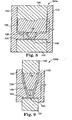
change memory cell 160a. In one embodiment, phase-change memory cell 160a is a tapered via phase-change memory cell. Phase-change memory cell 160a includesfirst electrode 122, phase-change material 134,second electrode 130, andinsulation material 132. Phase-change material 134 provides a storage location for storing one bit, 1.5 bits, two bits, or several bits of data. Phase-change material 134 is laterally completely enclosed byinsulation material 132, which defines the current path and hence the location of the phase change region in phase-change material 134. In one embodiment, each of thememory cells 106a-106d is similar to phase-change memory cell 160a. - Phase-
change material 134 includes afirst portion 124 in contact withfirst electrode 122, asecond portion 128 in contact withsecond electrode 130, and athird portion 126 contactingfirst portion 124 at 138 andsecond portion 128.First portion 124 of phase-change material 134 has a width or cross-section equal to the width or cross-section offirst electrode 122.Third portion 126 of phase-change material 134 laterally completely surroundssecond portion 128 of phase-change material 134. Thelower part 127 ofsecond portion 128 of phase-change material 134 has tapered sidewalls and has a maximum width or cross-section at 136 and a minimum width or cross-section near 138. -
First portion 124 of phase-change material 134 includes a first phase-change material composition.Second portion 128 of phase-change material 134 includes a second phase-change material composition, andthird portion 126 of phase-change material 134 includes a third phase-change material composition. The first, second, and third phase-change material compositions are constant. In one embodiment, the phase-change material composition offirst portion 124 includes the same phase-change material composition assecond portion 128. In other embodiments, the phase-change material composition offirst portion 124 is different from the phase-change material composition ofsecond portion 128. -
First portion 124 andsecond portion 128 of phase-change material 134 have a lower resistivity and preferably have a lower thermal conductivity and a higher melting temperature thanthird portion 126 of phase-change material 134 due to the phase-change materials selected. Therefore,first portion 124 andsecond portion 128 thermally insulatefirst electrode 122 andsecond electrode 130, respectively, such that the active phase-change region is confined tothird portion 126. In particular, the active phase-change region is confined to the phase-change material betweenfirst portion 124 at 138 and thelower part 127 ofsecond portion 128. By adjusting the amount of phase-change material deposited forthird portion 126, the size ofsecond portion 128 andthird portion 126 can be adjusted to achieve a desired size for the active region. Also, by adjusting the amount and type of phase-change material deposited forthird portion 126, phase-change memory cell 160a can be optimized for multi-bit data storage. - During operation of phase-
change memory cell 160a, a write pulse is applied betweenfirst electrode 122 andsecond electrode 130 to program phase-change memory cell 160a. Sincefirst portion 124 andsecond portion 128 of phase-change material 134 insulatethird portion 126 of phase-change material 134, the highest temperature within phase-change material 134 during a write pulse is withinthird portion 126. In addition, due to the higher resistivity ofthird portion 126, more heat is generated withinthird portion 126 than withinfirst portion 124 andsecond portion 128. Phase-change memory cell 160a operates similarly to phase-change memory cell 120a. - Figure 9 illustrates a cross-sectional view of another embodiment of a phase-
change memory cell 160b. In one embodiment, phase-change memory cell 160b is a tapered via phase-change memory cell. Phase-change memory cell 160b includesfirst electrode 122, phase-change material 134,second electrode 130, andinsulation material 132. Phase-change material 134 provides a storage location for storing one bit, 1.5 bits, two bits, or several bits of data. Phase-change material 134 is laterally completely enclosed byinsulation material 132, which defines the current path and hence the location of the phase change region in phase-change material 134. In one embodiment, each of thememory cells 106a-106d is similar to phase-change memory cell 160b. - Phase-
change material 134 includes afirst portion 124 in contact withfirst electrode 122, asecond portion 128 in contact withsecond electrode 130 at 146, and athird portion 126 contactingfirst portion 124 at 140 andsecond portion 128.First portion 124 of phase-change material 134 has the same width or cross-section asfirst electrode 122.Second portion 128 of phase-change material 134 has a maximum width or cross-section at 146 and a minimum width or cross-section at 148.Third portion 126 of phase-change material 134 laterally completely surroundssecond portion 128 of phase-change material 134. In one embodiment,second portion 128 of phase-change material 134 has tapered sidewalls. -
Portions change material 134 of phase-change memory cell 160b have similar phase-change material compositions and functions as the correspondingportions change memory cell 160a previously described and illustrated with reference to Figure 8. Phase-change memory cell 160b operates similarly to phase-change memory cell 120a. - Figure 10 illustrates a cross-sectional view of another embodiment of a phase-
change memory cell 170. In one embodiment, phase-change memory cell 170 is a bridge phase-change memory cell. Phase-change memory cell 170 includesfirst electrode 122, afirst contact 172, phase-change material 134, asecond contact 176, aspacer 174,second electrode 130, anddielectric material 132. Phase-change material 134 provides a storage location for storing one bit, 1.5 bits, two bits, or several bits of data. - Phase-
change material 134 includes afirst portion 124 in contact withfirst contact 172 and asecond portion 128 in contact withsecond contact 176 separated byspacer 174. First contact 172 contactsfirst electrode 122 andsecond contact 176 contactssecond electrode 130.First portion 124 of phase-change material 134 includes a first phase-change material composition.Second portion 128 of phase-change material 134 includes a second phase-change material composition. -
First portion 124 of phase-change material 134 has a lower resistivity and preferably has a lower thermal conductivity and a higher melting temperature thansecond portion 128 of phase-change material 134 due to the phase-change materials selected. Therefore,first portion 124 thermally insulatesfirst contact 172, such that the active phase-change region is confined tosecond portion 128. By adjusting the amount and type of phase-change material deposited forsecond portion 128, phase-change memory cell 170 can be optimized for multi-bit data storage. - During operation of phase-
change memory cell 170, a write pulse is applied between first contact 171 andsecond contact 176 to program phase-change memory cell 170. Sincefirst portion 124 insulatessecond portion 128 of phase-change material 134, the highest temperature within phase-change material 134 during a write pulse is withinsecond portion 128. In addition, due to the higher resistivity ofsecond portion 128, more heat is generated withinsecond portion 128 than withinfirst portion 124. Phase-change memory cell 170 operates similarly to phase-change memory cell 120a. - Embodiments of the present invention provide a phase-change memory cell including phase-change material having three portions. The first portion of the phase-change material insulates the first electrode, and the second portion of the phase-change material insulates the second electrode. The third portion of the phase-change material, which is insulated by the first portion and the third portion, is the active region. By controlling the volume of the active region and thermally insulating the active region, the reset current of the phase-change memory cell can be reduced. In addition, control of multi-bit data storage within the phase-change memory cell can be improved.
Claims (28)
- A memory cell comprising:a first electrode;a second electrode;a first portion of phase-change material contacting the first electrode;a second portion of phase-change material contacting the second electrode; anda third portion of phase-change material between the first portion and the second portion,wherein a phase-change material composition of the third portion and the second portion gradually transitions from the third portion to the second portion.
- The memory cell of claim 1, wherein a phase-change material composition of the first portion and the third portion gradually transitions from the first portion to the third portion.
- The memory cell of claim 1, wherein the first portion has a first resistivity, the second portion has a second resistivity, and the third portion has a third resistivity greater than the first resistivity and the second resistivity.
- The memory cell of claim 1, wherein the first portion has a first melting temperature, the second portion has a second melting temperature, and the third portion has a third melting temperature less than the first melting temperature and the second melting temperature.
- The memory cell of claim 1, wherein the phase-change material composition of the third portion and the second portion gradually transitions from the third portion comprising a doped phase-change material to the second portion comprising a differently doped or undoped phase-change material.
- The memory cell of claim 1, wherein the first portion, the second portion, and the third portion each comprises at least one of Ge, Sb, Te, Ga, As, In, Se, and S.
- A memory cell comprising:a first electrode;a second electrode;a first portion of phase-change material contacting the first electrode;a second portion of phase-change material contacting the second electrode; anda third portion of phase-change material contacting the first portion and the second portion and laterally surrounding the second portion.
- The memory cell of claim 7, wherein the first portion has a first resistivity, the second portion has a second resistivity, and the third portion has a third resistivity greater than the first resistivity and the second resistivity.
- The memory cell of claim 7, wherein the first portion has a first melting temperature, the second portion has a second melting temperature, and the third portion has a third melting temperature less than the first melting temperature and the second melting temperature.
- The memory cell of claim 7, wherein the third portion comprises a doped phase-change material and the first portion and the second portion comprise a differently doped or undoped phase-change material.
- The memory cell of claim 7, wherein the first portion, the second portion, and the third portion each comprises at least one of Ge, Sb, Te, Ga, As, In, Se, and S.
- A memory cell comprising:a first electrode;a second electrode;phase-change material contacting the first electrode and the second electrode; andmeans for controlling a size of an active region of the phase-change material.
- The memory cell of claim 12, wherein the phase-change material is configured for storing at least three resistance levels.
- The memory cell of claim 12, wherein the phase-change material comprises at least one of Ge, Sb, Te, Ga, As, In, Se, and S.
- A method for fabricating a memory cell, the method comprising:providing a first electrode;depositing a first portion of phase-change material over the first electrode;depositing a second portion of phase-change material over the first portion while gradually transitioning a phase-change material composition of the second portion to provide a third portion of phase-change material over the second portion; anddepositing a second electrode over the third portion.
- The method of claim 15, wherein depositing the first portion comprises gradually transitioning a phase-change material composition of the first portion to provide the second portion.
- The method of claim 15, wherein depositing the first portion comprises depositing the first portion of phase-change material having a first resistivity; and
wherein depositing the second portion comprises depositing the second portion of phase-change material having a second resistivity greater than the first resistivity while gradually transitioning the phase-change material composition of the second portion to provide a third portion of phase-change material having a third resistivity less than the second resistivity. - The method of claim 15, wherein depositing the first portion comprises depositing the first portion of phase-change material having a first melting temperature; and
wherein depositing the second portion comprises depositing the second portion of phase-change material having a second melting temperature less than the first melting temperature while gradually transitioning the phase-change material composition of the second portion to provide a third portion of phase-change material having a third melting temperature greater than the second melting temperature. - The method of claim 15, wherein depositing the second portion comprises depositing the second portion while gradually varying a doping level of the phase-change material composition.
- A method for fabricating a memory cell, the method comprising:providing a first electrode;providing a second electrode;providing a first portion of phase-change material contacting the first electrode;providing a second portion of phase-change material contacting the second electrode; andproviding a third portion of phase-change material contacting the first portion and the second portion and laterally surrounding the second portion.
- The memory cell of claim 20, wherein providing the first portion comprises providing the first portion having a first resistivity;
wherein providing the second portion comprises providing the second portion having a second resistivity; and
wherein providing the third portion comprises providing the third portion having a third resistivity greater than the first resistivity and the second resistivity. - The memory cell of claim 20, wherein providing the first portion comprises providing the first portion having a first melting temperature;
wherein providing the second portion comprises providing the second portion having a second melting temperature; and
wherein providing the third portion comprises providing the third portion having a third melting temperature less than the first melting temperature and the second melting temperature. - The memory cell of claim 20, wherein providing the third portion comprises providing the third portion comprising a chalcogenide material;
wherein providing the first portion comprises providing the first portion comprising the chalcogenide material doped with another material; and
wherein providing the second portion comprises providing the second portion comprising the chalcogenide material doped with another material. - The memory cell of claim 20, wherein providing the second portion comprises providing the second portion having a same phase-change material composition as the first portion.
- A memory cell comprising:a first electrode;a first contact contacting the first electrode;a second electrode;a second contact contacting the second electrode;a first portion of phase-change material contacting the first contact; anda second portion of phase-change material contacting the first portion and the second contact.
- The memory cell of claim 25, wherein the first portion has a first resistivity and the second portion has a second resistivity greater than the first resistivity.
- The memory cell of claim 25, wherein the first portion has a first melting temperature and the second portion has a second melting temperature less than the first melting temperature.
- The memory cell of claim 25, wherein the first portion and the second portion each comprises at least one of Ge, Sb, Te, Ga, As, In, Se, and S.
Applications Claiming Priority (1)
| Application Number | Priority Date | Filing Date | Title |
|---|---|---|---|
| US11/265,377 US7973384B2 (en) | 2005-11-02 | 2005-11-02 | Phase change memory cell including multiple phase change material portions |
Publications (3)
| Publication Number | Publication Date |
|---|---|
| EP1783844A2 true EP1783844A2 (en) | 2007-05-09 |
| EP1783844A3 EP1783844A3 (en) | 2010-12-08 |
| EP1783844B1 EP1783844B1 (en) | 2012-09-26 |
Family
ID=37698169
Family Applications (1)
| Application Number | Title | Priority Date | Filing Date |
|---|---|---|---|
| EP06021708A Expired - Fee Related EP1783844B1 (en) | 2005-11-02 | 2006-10-17 | Phase change memory cell including multiple phase change material portions |
Country Status (3)
| Country | Link |
|---|---|
| US (1) | US7973384B2 (en) |
| EP (1) | EP1783844B1 (en) |
| KR (1) | KR100856505B1 (en) |
Cited By (8)
| Publication number | Priority date | Publication date | Assignee | Title |
|---|---|---|---|---|
| EP1879232A2 (en) | 2006-07-10 | 2008-01-16 | Qimonda North America Corp. | Low power phase change memory cell having different phase change materials |
| WO2009130668A1 (en) * | 2008-04-21 | 2009-10-29 | Nxp B.V. | Phase-change-material memory with multibit memory cells and method for fabricating the same |
| EP2117058A1 (en) * | 2008-05-08 | 2009-11-11 | Macronix International Co., Ltd. | Phase change device having two or more substantially amorphous regions in high resistance state |
| EP2002491B1 (en) * | 2006-03-17 | 2011-10-19 | Micron Technology, Inc. | Reduced power consumption phase change memory and methods for forming the same |
| CN104934531A (en) * | 2014-03-17 | 2015-09-23 | 爱思开海力士有限公司 | Method of fabricating semiconductor integrated circuit having phase-change layer |
| JP2021513221A (en) * | 2018-02-09 | 2021-05-20 | マイクロン テクノロジー,インク. | Dopant Modulated Etching for Memory Devices |
| US11545625B2 (en) | 2018-02-09 | 2023-01-03 | Micron Technology, Inc. | Tapered memory cell profiles |
| US11735261B2 (en) | 2017-04-28 | 2023-08-22 | Micron Technology, Inc. | Programming enhancement in self-selecting memory |
Families Citing this family (53)
| Publication number | Priority date | Publication date | Assignee | Title |
|---|---|---|---|---|
| US7767992B2 (en) * | 2005-08-09 | 2010-08-03 | Ovonyx, Inc. | Multi-layer chalcogenide devices |
| US7786460B2 (en) * | 2005-11-15 | 2010-08-31 | Macronix International Co., Ltd. | Phase change memory device and manufacturing method |
| US7688619B2 (en) | 2005-11-28 | 2010-03-30 | Macronix International Co., Ltd. | Phase change memory cell and manufacturing method |
| US7459717B2 (en) * | 2005-11-28 | 2008-12-02 | Macronix International Co., Ltd. | Phase change memory cell and manufacturing method |
| US8896045B2 (en) * | 2006-04-19 | 2014-11-25 | Infineon Technologies Ag | Integrated circuit including sidewall spacer |
| KR100822808B1 (en) * | 2006-11-02 | 2008-04-17 | 삼성전자주식회사 | Phase change memory device and method of formign the same |
| KR20080055508A (en) * | 2006-12-15 | 2008-06-19 | 삼성전자주식회사 | Phase change layer having different crystal lattice in single layer and method of forming the same and phase change memory device comprising means for preventing ti diffusion and method of manufacturing the same |
| US7462858B2 (en) * | 2007-01-29 | 2008-12-09 | International Business Machines Corporation | Fabrication of phase change memory element with phase-change electrodes using conformal deposition |
| US7456460B2 (en) * | 2007-01-29 | 2008-11-25 | International Business Machines Corporation | Phase change memory element and method of making the same |
| KR100810617B1 (en) * | 2007-02-09 | 2008-03-06 | 삼성전자주식회사 | Multi bit pram and method of fabricating the same |
| KR100819560B1 (en) * | 2007-03-26 | 2008-04-08 | 삼성전자주식회사 | Phase change memory device and method of fabricating the same |
| US7704788B2 (en) * | 2007-04-06 | 2010-04-27 | Samsung Electronics Co., Ltd. | Methods of fabricating multi-bit phase-change memory devices and devices formed thereby |
| US7812333B2 (en) * | 2007-06-28 | 2010-10-12 | Qimonda North America Corp. | Integrated circuit including resistivity changing material having a planarized surface |
| US7964861B2 (en) * | 2007-11-06 | 2011-06-21 | Ovonyx, Inc. | Method and apparatus for reducing programmed volume of phase change memory |
| US7989793B2 (en) | 2007-12-10 | 2011-08-02 | Electronics And Telecommunications Research Institute | Electrical device using phase change material, phase change memory device using solid state reaction and method for fabricating the same |
| KR100998887B1 (en) * | 2007-12-10 | 2010-12-08 | 한국전자통신연구원 | The electrical device using phase change material, the phase change memory device, and the method for fabricating the same |
| US7852658B2 (en) * | 2008-03-14 | 2010-12-14 | Micron Technology, Inc. | Phase change memory cell with constriction structure |
| WO2009122347A2 (en) | 2008-04-01 | 2009-10-08 | Nxp B.V. | Multiple bit phase change memory cell |
| KR20090117103A (en) * | 2008-05-08 | 2009-11-12 | 삼성전자주식회사 | Phase change memory device |
| KR100990215B1 (en) * | 2008-07-17 | 2010-10-29 | 한국전자통신연구원 | Phase Change Type Memory and Method for Fabricating the Same |
| US7903457B2 (en) | 2008-08-19 | 2011-03-08 | Macronix International Co., Ltd. | Multiple phase change materials in an integrated circuit for system on a chip application |
| US8124950B2 (en) | 2008-08-26 | 2012-02-28 | International Business Machines Corporation | Concentric phase change memory element |
| US8324605B2 (en) | 2008-10-02 | 2012-12-04 | Macronix International Co., Ltd. | Dielectric mesh isolated phase change structure for phase change memory |
| KR20100058909A (en) * | 2008-11-25 | 2010-06-04 | 삼성전자주식회사 | Method of forming resistance changable memory device |
| US8148707B2 (en) * | 2008-12-30 | 2012-04-03 | Stmicroelectronics S.R.L. | Ovonic threshold switch film composition for TSLAGS material |
| US8386883B2 (en) * | 2009-02-24 | 2013-02-26 | International Business Machines Corporation | Lengthening life of a limited life memory |
| US8809829B2 (en) * | 2009-06-15 | 2014-08-19 | Macronix International Co., Ltd. | Phase change memory having stabilized microstructure and manufacturing method |
| US8363463B2 (en) | 2009-06-25 | 2013-01-29 | Macronix International Co., Ltd. | Phase change memory having one or more non-constant doping profiles |
| US8138056B2 (en) | 2009-07-03 | 2012-03-20 | International Business Machines Corporation | Thermally insulated phase change material memory cells with pillar structure |
| KR20110015934A (en) * | 2009-08-10 | 2011-02-17 | 삼성전자주식회사 | Nonvolatile memory device and programming method thereof |
| DE102010061572A1 (en) | 2009-12-29 | 2011-07-14 | Samsung Electronics Co., Ltd., Kyonggi | Phase change structure, method of forming a phase change layer, phase change memory device, and method of manufacturing a phase change memory device |
| US8426242B2 (en) | 2011-02-01 | 2013-04-23 | Macronix International Co., Ltd. | Composite target sputtering for forming doped phase change materials |
| US8946666B2 (en) | 2011-06-23 | 2015-02-03 | Macronix International Co., Ltd. | Ge-Rich GST-212 phase change memory materials |
| JP5611903B2 (en) * | 2011-08-09 | 2014-10-22 | 株式会社東芝 | Resistance change memory |
| US8932901B2 (en) | 2011-10-31 | 2015-01-13 | Macronix International Co., Ltd. | Stressed phase change materials |
| FR2995443B1 (en) * | 2012-09-10 | 2014-09-26 | St Microelectronics Crolles 2 | MEMORY CELL WITH PHASE CHANGE |
| US9059130B2 (en) | 2012-12-31 | 2015-06-16 | International Business Machines Corporation | Phase changing on-chip thermal heat sink |
| CN104966717B (en) | 2014-01-24 | 2018-04-13 | 旺宏电子股份有限公司 | A kind of storage arrangement and the method that the storage arrangement is provided |
| US9627612B2 (en) | 2014-02-27 | 2017-04-18 | International Business Machines Corporation | Metal nitride keyhole or spacer phase change memory cell structures |
| KR102212377B1 (en) | 2014-06-16 | 2021-02-04 | 삼성전자주식회사 | Method of manufacturing a phase-change memory device |
| US9672906B2 (en) | 2015-06-19 | 2017-06-06 | Macronix International Co., Ltd. | Phase change memory with inter-granular switching |
| WO2018056963A1 (en) * | 2016-09-21 | 2018-03-29 | Intel Corporation | Conductive bridge random access memory (cbram) devices with graded conductivity electrolyte layer |
| US10693065B2 (en) | 2018-02-09 | 2020-06-23 | Micron Technology, Inc. | Tapered cell profile and fabrication |
| US10541364B2 (en) | 2018-02-09 | 2020-01-21 | Micron Technology, Inc. | Memory cells with asymmetrical electrode interfaces |
| US10454025B1 (en) * | 2018-06-13 | 2019-10-22 | International Business Machines Corporation | Phase change memory with gradual resistance change |
| KR20200022945A (en) * | 2018-08-24 | 2020-03-04 | 삼성전자주식회사 | Variable resistance memory device |
| KR102549544B1 (en) * | 2018-09-03 | 2023-06-29 | 삼성전자주식회사 | Memory devices |
| US11367833B2 (en) * | 2018-09-28 | 2022-06-21 | Intel Corporation | Memory cells having increased structural stability |
| CN112310278B (en) * | 2019-07-31 | 2024-03-08 | 华邦电子股份有限公司 | Variable resistance memory and manufacturing method thereof |
| US11380843B2 (en) | 2020-02-13 | 2022-07-05 | International Business Machines Corporation | Phase change memory using multiple stacks of PCM materials |
| US11683998B2 (en) | 2021-03-22 | 2023-06-20 | International Business Machines Corporation | Vertical phase change bridge memory cell |
| US11903333B2 (en) | 2021-05-27 | 2024-02-13 | Micron Technology, Inc. | Sidewall structures for memory cells in vertical structures |
| US11957068B2 (en) | 2021-05-27 | 2024-04-09 | Micron Technology, Inc. | Memory cells with sidewall and bulk regions in vertical structures |
Family Cites Families (18)
| Publication number | Priority date | Publication date | Assignee | Title |
|---|---|---|---|---|
| US4177475A (en) | 1977-10-31 | 1979-12-04 | Burroughs Corporation | High temperature amorphous memory device for an electrically alterable read-only memory |
| US5534712A (en) | 1991-01-18 | 1996-07-09 | Energy Conversion Devices, Inc. | Electrically erasable memory elements characterized by reduced current and improved thermal stability |
| US6985378B2 (en) * | 1998-12-04 | 2006-01-10 | Axon Technologies Corporation | Programmable microelectronic device, structure, and system and method of forming the same |
| US6507061B1 (en) | 2001-08-31 | 2003-01-14 | Intel Corporation | Multiple layer phase-change memory |
| DE60220245D1 (en) | 2002-01-17 | 2007-07-05 | St Microelectronics Srl | Integrated resistance element, phase change Storage element with such resistance element, and method for its production |
| US6849868B2 (en) * | 2002-03-14 | 2005-02-01 | Micron Technology, Inc. | Methods and apparatus for resistance variable material cells |
| US6579760B1 (en) * | 2002-03-28 | 2003-06-17 | Macronix International Co., Ltd. | Self-aligned, programmable phase change memory |
| US6856002B2 (en) * | 2002-08-29 | 2005-02-15 | Micron Technology, Inc. | Graded GexSe100-x concentration in PCRAM |
| KR20040047272A (en) * | 2002-11-29 | 2004-06-05 | 삼성전자주식회사 | Phase changing type semiconductor memory device |
| US7115927B2 (en) | 2003-02-24 | 2006-10-03 | Samsung Electronics Co., Ltd. | Phase changeable memory devices |
| US6838692B1 (en) | 2003-06-23 | 2005-01-04 | Macronix International Co., Ltd. | Chalcogenide memory device with multiple bits per cell |
| US7893419B2 (en) * | 2003-08-04 | 2011-02-22 | Intel Corporation | Processing phase change material to improve programming speed |
| US7381611B2 (en) | 2003-08-04 | 2008-06-03 | Intel Corporation | Multilayered phase change memory |
| US6927410B2 (en) | 2003-09-04 | 2005-08-09 | Silicon Storage Technology, Inc. | Memory device with discrete layers of phase change memory material |
| US7485891B2 (en) | 2003-11-20 | 2009-02-03 | International Business Machines Corporation | Multi-bit phase change memory cell and multi-bit phase change memory including the same, method of forming a multi-bit phase change memory, and method of programming a multi-bit phase change memory |
| KR20050059855A (en) * | 2003-12-15 | 2005-06-21 | 삼성전자주식회사 | Phase change memory device and method of fabricating the same |
| KR100568543B1 (en) * | 2004-08-31 | 2006-04-07 | 삼성전자주식회사 | Method of forming a phase change memory device having a small area of contact |
| US7372725B2 (en) * | 2005-08-15 | 2008-05-13 | Infineon Technologies Ag | Integrated circuit having resistive memory |
-
2005
- 2005-11-02 US US11/265,377 patent/US7973384B2/en not_active Expired - Fee Related
-
2006
- 2006-10-17 EP EP06021708A patent/EP1783844B1/en not_active Expired - Fee Related
- 2006-11-02 KR KR1020060107906A patent/KR100856505B1/en not_active IP Right Cessation
Non-Patent Citations (1)
| Title |
|---|
| None |
Cited By (12)
| Publication number | Priority date | Publication date | Assignee | Title |
|---|---|---|---|---|
| EP2002491B1 (en) * | 2006-03-17 | 2011-10-19 | Micron Technology, Inc. | Reduced power consumption phase change memory and methods for forming the same |
| EP1879232A2 (en) | 2006-07-10 | 2008-01-16 | Qimonda North America Corp. | Low power phase change memory cell having different phase change materials |
| EP1879232A3 (en) * | 2006-07-10 | 2011-08-10 | Qimonda North America Corp. | Low power phase change memory cell having different phase change materials |
| WO2009130668A1 (en) * | 2008-04-21 | 2009-10-29 | Nxp B.V. | Phase-change-material memory with multibit memory cells and method for fabricating the same |
| EP2117058A1 (en) * | 2008-05-08 | 2009-11-11 | Macronix International Co., Ltd. | Phase change device having two or more substantially amorphous regions in high resistance state |
| US8059449B2 (en) | 2008-05-08 | 2011-11-15 | Macronix International Co., Ltd. | Phase change device having two or more substantial amorphous regions in high resistance state |
| CN101577140B (en) * | 2008-05-08 | 2012-03-28 | 旺宏电子股份有限公司 | Memory device and operating method thereof |
| CN104934531A (en) * | 2014-03-17 | 2015-09-23 | 爱思开海力士有限公司 | Method of fabricating semiconductor integrated circuit having phase-change layer |
| US11735261B2 (en) | 2017-04-28 | 2023-08-22 | Micron Technology, Inc. | Programming enhancement in self-selecting memory |
| JP2021513221A (en) * | 2018-02-09 | 2021-05-20 | マイクロン テクノロジー,インク. | Dopant Modulated Etching for Memory Devices |
| US11545625B2 (en) | 2018-02-09 | 2023-01-03 | Micron Technology, Inc. | Tapered memory cell profiles |
| US11800816B2 (en) | 2018-02-09 | 2023-10-24 | Micron Technology, Inc. | Dopant-modulated etching for memory devices |
Also Published As
| Publication number | Publication date |
|---|---|
| US7973384B2 (en) | 2011-07-05 |
| KR20070047724A (en) | 2007-05-07 |
| EP1783844B1 (en) | 2012-09-26 |
| KR100856505B1 (en) | 2008-09-04 |
| US20070097739A1 (en) | 2007-05-03 |
| EP1783844A3 (en) | 2010-12-08 |
Similar Documents
| Publication | Publication Date | Title |
|---|---|---|
| US7973384B2 (en) | Phase change memory cell including multiple phase change material portions | |
| US8084799B2 (en) | Integrated circuit with memory having a step-like programming characteristic | |
| EP1780814B1 (en) | Phase change memory cell | |
| US7417245B2 (en) | Phase change memory having multilayer thermal insulation | |
| US7688618B2 (en) | Integrated circuit having memory having a step-like programming characteristic | |
| US7973301B2 (en) | Low power phase change memory cell with large read signal | |
| US7824951B2 (en) | Method of fabricating an integrated circuit having a memory including a low-k dielectric material | |
| US20070267620A1 (en) | Memory cell including doped phase change material | |
| US20080019257A1 (en) | Integrated circuit with resistivity changing material having a step-like programming characteristitic | |
| US8189372B2 (en) | Integrated circuit including electrode having recessed portion | |
| US7759770B2 (en) | Integrated circuit including memory element with high speed low current phase change material | |
| US8003971B2 (en) | Integrated circuit including memory element doped with dielectric material | |
| EP1923928A2 (en) | Phase change memory cell having a sidewall contact | |
| US8189374B2 (en) | Memory device including an electrode having an outer portion with greater resistivity | |
| US7812333B2 (en) | Integrated circuit including resistivity changing material having a planarized surface | |
| EP1732148A1 (en) | Phase change memory cell having ring contacts | |
| US7671353B2 (en) | Integrated circuit having contact including material between sidewalls | |
| US7679074B2 (en) | Integrated circuit having multilayer electrode | |
| US7939817B2 (en) | Integrated circuit including memory element with spatially stable material | |
| US8009468B2 (en) | Method for fabricating an integrated circuit including memory element with spatially stable material |
Legal Events
| Date | Code | Title | Description |
|---|---|---|---|
| PUAI | Public reference made under article 153(3) epc to a published international application that has entered the european phase |
Free format text: ORIGINAL CODE: 0009012 |
|
| 17P | Request for examination filed |
Effective date: 20061017 |
|
| AK | Designated contracting states |
Kind code of ref document: A2 Designated state(s): AT BE BG CH CY CZ DE DK EE ES FI FR GB GR HU IE IS IT LI LT LU LV MC NL PL PT RO SE SI SK TR |
|
| AX | Request for extension of the european patent |
Extension state: AL BA HR MK YU |
|
| 19U | Interruption of proceedings before grant |
Effective date: 20090401 |
|
| 19W | Proceedings resumed before grant after interruption of proceedings |
Effective date: 20091123 |
|
| PUAL | Search report despatched |
Free format text: ORIGINAL CODE: 0009013 |
|
| AK | Designated contracting states |
Kind code of ref document: A3 Designated state(s): AT BE BG CH CY CZ DE DK EE ES FI FR GB GR HU IE IS IT LI LT LU LV MC NL PL PT RO SE SI SK TR |
|
| AX | Request for extension of the european patent |
Extension state: AL BA HR MK RS |
|
| AKX | Designation fees paid |
Designated state(s): DE FR GB IT |
|
| 17Q | First examination report despatched |
Effective date: 20110802 |
|
| GRAP | Despatch of communication of intention to grant a patent |
Free format text: ORIGINAL CODE: EPIDOSNIGR1 |
|
| GRAS | Grant fee paid |
Free format text: ORIGINAL CODE: EPIDOSNIGR3 |
|
| GRAA | (expected) grant |
Free format text: ORIGINAL CODE: 0009210 |
|
| AK | Designated contracting states |
Kind code of ref document: B1 Designated state(s): DE FR GB IT |
|
| REG | Reference to a national code |
Ref country code: GB Ref legal event code: FG4D Ref country code: DE Ref legal event code: R081 Ref document number: 602006032114 Country of ref document: DE Owner name: INFINEON TECHNOLOGIES AG, DE Free format text: FORMER OWNER: QIMONDA AG, 81739 MUENCHEN, DE Ref country code: DE Ref legal event code: R081 Ref document number: 602006032114 Country of ref document: DE Owner name: POLARIS INNOVATIONS LTD., IE Free format text: FORMER OWNER: QIMONDA AG, 81739 MUENCHEN, DE |
|
| REG | Reference to a national code |
Ref country code: DE Ref legal event code: R096 Ref document number: 602006032114 Country of ref document: DE Effective date: 20121122 |
|
| PLBE | No opposition filed within time limit |
Free format text: ORIGINAL CODE: 0009261 |
|
| STAA | Information on the status of an ep patent application or granted ep patent |
Free format text: STATUS: NO OPPOSITION FILED WITHIN TIME LIMIT |
|
| PG25 | Lapsed in a contracting state [announced via postgrant information from national office to epo] |
Ref country code: IT Free format text: LAPSE BECAUSE OF FAILURE TO SUBMIT A TRANSLATION OF THE DESCRIPTION OR TO PAY THE FEE WITHIN THE PRESCRIBED TIME-LIMIT Effective date: 20120926 |
|
| 26N | No opposition filed |
Effective date: 20130627 |
|
| REG | Reference to a national code |
Ref country code: DE Ref legal event code: R097 Ref document number: 602006032114 Country of ref document: DE Effective date: 20130627 |
|
| REG | Reference to a national code |
Ref country code: DE Ref legal event code: R081 Ref document number: 602006032114 Country of ref document: DE Owner name: INFINEON TECHNOLOGIES AG, DE Free format text: FORMER OWNER: QIMONDA AG, 81739 MUENCHEN, DE Ref country code: DE Ref legal event code: R081 Ref document number: 602006032114 Country of ref document: DE Owner name: POLARIS INNOVATIONS LTD., IE Free format text: FORMER OWNER: QIMONDA AG, 81739 MUENCHEN, DE |
|
| REG | Reference to a national code |
Ref country code: GB Ref legal event code: 732E Free format text: REGISTERED BETWEEN 20150827 AND 20150902 |
|
| REG | Reference to a national code |
Ref country code: DE Ref legal event code: R081 Ref document number: 602006032114 Country of ref document: DE Owner name: POLARIS INNOVATIONS LTD., IE Free format text: FORMER OWNER: INFINEON TECHNOLOGIES AG, 85579 NEUBIBERG, DE |
|
| REG | Reference to a national code |
Ref country code: FR Ref legal event code: PLFP Year of fee payment: 10 |
|
| REG | Reference to a national code |
Ref country code: FR Ref legal event code: TP Owner name: INFINEON TECHNOLOGIES AG, DE Effective date: 20160212 |
|
| REG | Reference to a national code |
Ref country code: FR Ref legal event code: PLFP Year of fee payment: 11 |
|
| PGFP | Annual fee paid to national office [announced via postgrant information from national office to epo] |
Ref country code: FR Payment date: 20160919 Year of fee payment: 11 |
|
| PGFP | Annual fee paid to national office [announced via postgrant information from national office to epo] |
Ref country code: GB Payment date: 20161012 Year of fee payment: 11 Ref country code: DE Payment date: 20161011 Year of fee payment: 11 |
|
| REG | Reference to a national code |
Ref country code: DE Ref legal event code: R119 Ref document number: 602006032114 Country of ref document: DE |
|
| GBPC | Gb: european patent ceased through non-payment of renewal fee |
Effective date: 20171017 |
|
| REG | Reference to a national code |
Ref country code: FR Ref legal event code: ST Effective date: 20180629 |
|
| PG25 | Lapsed in a contracting state [announced via postgrant information from national office to epo] |
Ref country code: DE Free format text: LAPSE BECAUSE OF NON-PAYMENT OF DUE FEES Effective date: 20180501 Ref country code: GB Free format text: LAPSE BECAUSE OF NON-PAYMENT OF DUE FEES Effective date: 20171017 |
|
| PG25 | Lapsed in a contracting state [announced via postgrant information from national office to epo] |
Ref country code: FR Free format text: LAPSE BECAUSE OF NON-PAYMENT OF DUE FEES Effective date: 20171031 |