EP1800752A1 - Sensing photon energies of optical signals - Google Patents
Sensing photon energies of optical signals Download PDFInfo
- Publication number
- EP1800752A1 EP1800752A1 EP06126519A EP06126519A EP1800752A1 EP 1800752 A1 EP1800752 A1 EP 1800752A1 EP 06126519 A EP06126519 A EP 06126519A EP 06126519 A EP06126519 A EP 06126519A EP 1800752 A1 EP1800752 A1 EP 1800752A1
- Authority
- EP
- European Patent Office
- Prior art keywords
- optical signal
- array
- photons
- cells
- optical
- Prior art date
- Legal status (The legal status is an assumption and is not a legal conclusion. Google has not performed a legal analysis and makes no representation as to the accuracy of the status listed.)
- Ceased
Links
- 230000003287 optical effect Effects 0.000 title claims abstract description 211
- 230000033001 locomotion Effects 0.000 claims abstract description 76
- 230000003595 spectral effect Effects 0.000 claims abstract description 31
- 238000000034 method Methods 0.000 claims description 62
- 230000005540 biological transmission Effects 0.000 claims description 57
- 238000000576 coating method Methods 0.000 claims description 17
- 239000011248 coating agent Substances 0.000 claims description 15
- 238000000018 DNA microarray Methods 0.000 claims description 10
- 238000009826 distribution Methods 0.000 claims description 10
- 239000012530 fluid Substances 0.000 claims description 10
- 230000005284 excitation Effects 0.000 claims description 8
- 239000012491 analyte Substances 0.000 claims description 3
- 238000005286 illumination Methods 0.000 description 20
- 230000006870 function Effects 0.000 description 13
- 239000000463 material Substances 0.000 description 13
- 239000010408 film Substances 0.000 description 10
- 238000000151 deposition Methods 0.000 description 9
- 238000002310 reflectometry Methods 0.000 description 9
- 230000008021 deposition Effects 0.000 description 8
- 239000002245 particle Substances 0.000 description 7
- 238000003491 array Methods 0.000 description 6
- 238000001228 spectrum Methods 0.000 description 6
- 238000010586 diagram Methods 0.000 description 5
- 230000004044 response Effects 0.000 description 5
- 239000000443 aerosol Substances 0.000 description 4
- 239000012634 fragment Substances 0.000 description 4
- 239000011521 glass Substances 0.000 description 4
- 230000003993 interaction Effects 0.000 description 4
- 239000007788 liquid Substances 0.000 description 4
- 230000008569 process Effects 0.000 description 4
- 230000008859 change Effects 0.000 description 3
- 238000003384 imaging method Methods 0.000 description 3
- 238000004519 manufacturing process Methods 0.000 description 3
- VYPSYNLAJGMNEJ-UHFFFAOYSA-N Silicium dioxide Chemical compound O=[Si]=O VYPSYNLAJGMNEJ-UHFFFAOYSA-N 0.000 description 2
- GWEVSGVZZGPLCZ-UHFFFAOYSA-N Titan oxide Chemical compound O=[Ti]=O GWEVSGVZZGPLCZ-UHFFFAOYSA-N 0.000 description 2
- 238000010521 absorption reaction Methods 0.000 description 2
- 238000004458 analytical method Methods 0.000 description 2
- 238000013459 approach Methods 0.000 description 2
- 238000000429 assembly Methods 0.000 description 2
- 230000000712 assembly Effects 0.000 description 2
- 230000008901 benefit Effects 0.000 description 2
- 230000005670 electromagnetic radiation Effects 0.000 description 2
- 230000008020 evaporation Effects 0.000 description 2
- 238000001704 evaporation Methods 0.000 description 2
- 230000035945 sensitivity Effects 0.000 description 2
- 238000004611 spectroscopical analysis Methods 0.000 description 2
- 239000000126 substance Substances 0.000 description 2
- 206010034960 Photophobia Diseases 0.000 description 1
- 239000003124 biologic agent Substances 0.000 description 1
- BJQHLKABXJIVAM-UHFFFAOYSA-N bis(2-ethylhexyl) phthalate Chemical compound CCCCC(CC)COC(=O)C1=CC=CC=C1C(=O)OCC(CC)CCCC BJQHLKABXJIVAM-UHFFFAOYSA-N 0.000 description 1
- 239000013043 chemical agent Substances 0.000 description 1
- 229910052681 coesite Inorganic materials 0.000 description 1
- 229910052906 cristobalite Inorganic materials 0.000 description 1
- 230000001419 dependent effect Effects 0.000 description 1
- 238000013461 design Methods 0.000 description 1
- 239000006185 dispersion Substances 0.000 description 1
- 230000000694 effects Effects 0.000 description 1
- 238000005530 etching Methods 0.000 description 1
- 230000002349 favourable effect Effects 0.000 description 1
- 238000002189 fluorescence spectrum Methods 0.000 description 1
- -1 gasses Substances 0.000 description 1
- 230000010354 integration Effects 0.000 description 1
- 230000002452 interceptive effect Effects 0.000 description 1
- 208000013469 light sensitivity Diseases 0.000 description 1
- 238000004020 luminiscence type Methods 0.000 description 1
- 239000011159 matrix material Substances 0.000 description 1
- 239000002184 metal Substances 0.000 description 1
- 239000007769 metal material Substances 0.000 description 1
- 230000005693 optoelectronics Effects 0.000 description 1
- 238000000059 patterning Methods 0.000 description 1
- 230000002093 peripheral effect Effects 0.000 description 1
- 238000005424 photoluminescence Methods 0.000 description 1
- 239000004038 photonic crystal Substances 0.000 description 1
- 238000007747 plating Methods 0.000 description 1
- 238000005498 polishing Methods 0.000 description 1
- 238000007639 printing Methods 0.000 description 1
- 238000004886 process control Methods 0.000 description 1
- 238000012545 processing Methods 0.000 description 1
- 230000001902 propagating effect Effects 0.000 description 1
- 230000005855 radiation Effects 0.000 description 1
- 230000000630 rising effect Effects 0.000 description 1
- 239000004065 semiconductor Substances 0.000 description 1
- 239000000377 silicon dioxide Substances 0.000 description 1
- 239000007787 solid Substances 0.000 description 1
- 238000004528 spin coating Methods 0.000 description 1
- 230000007480 spreading Effects 0.000 description 1
- 238000003892 spreading Methods 0.000 description 1
- 238000004544 sputter deposition Methods 0.000 description 1
- 229910052682 stishovite Inorganic materials 0.000 description 1
- 239000000758 substrate Substances 0.000 description 1
- 230000001629 suppression Effects 0.000 description 1
- PBCFLUZVCVVTBY-UHFFFAOYSA-N tantalum pentoxide Inorganic materials O=[Ta](=O)O[Ta](=O)=O PBCFLUZVCVVTBY-UHFFFAOYSA-N 0.000 description 1
- 239000010409 thin film Substances 0.000 description 1
- 238000012546 transfer Methods 0.000 description 1
- 229910052905 tridymite Inorganic materials 0.000 description 1
Images


Classifications
-
- G—PHYSICS
- G01—MEASURING; TESTING
- G01J—MEASUREMENT OF INTENSITY, VELOCITY, SPECTRAL CONTENT, POLARISATION, PHASE OR PULSE CHARACTERISTICS OF INFRARED, VISIBLE OR ULTRAVIOLET LIGHT; COLORIMETRY; RADIATION PYROMETRY
- G01J3/00—Spectrometry; Spectrophotometry; Monochromators; Measuring colours
- G01J3/12—Generating the spectrum; Monochromators
- G01J3/26—Generating the spectrum; Monochromators using multiple reflection, e.g. Fabry-Perot interferometer, variable interference filters
-
- G—PHYSICS
- G01—MEASURING; TESTING
- G01J—MEASUREMENT OF INTENSITY, VELOCITY, SPECTRAL CONTENT, POLARISATION, PHASE OR PULSE CHARACTERISTICS OF INFRARED, VISIBLE OR ULTRAVIOLET LIGHT; COLORIMETRY; RADIATION PYROMETRY
- G01J3/00—Spectrometry; Spectrophotometry; Monochromators; Measuring colours
- G01J3/28—Investigating the spectrum
- G01J3/2803—Investigating the spectrum using photoelectric array detector
-
- G—PHYSICS
- G01—MEASURING; TESTING
- G01N—INVESTIGATING OR ANALYSING MATERIALS BY DETERMINING THEIR CHEMICAL OR PHYSICAL PROPERTIES
- G01N21/00—Investigating or analysing materials by the use of optical means, i.e. using sub-millimetre waves, infrared, visible or ultraviolet light
- G01N21/62—Systems in which the material investigated is excited whereby it emits light or causes a change in wavelength of the incident light
- G01N21/63—Systems in which the material investigated is excited whereby it emits light or causes a change in wavelength of the incident light optically excited
- G01N21/64—Fluorescence; Phosphorescence
- G01N21/645—Specially adapted constructive features of fluorimeters
-
- B—PERFORMING OPERATIONS; TRANSPORTING
- B01—PHYSICAL OR CHEMICAL PROCESSES OR APPARATUS IN GENERAL
- B01L—CHEMICAL OR PHYSICAL LABORATORY APPARATUS FOR GENERAL USE
- B01L3/00—Containers or dishes for laboratory use, e.g. laboratory glassware; Droppers
- B01L3/50—Containers for the purpose of retaining a material to be analysed, e.g. test tubes
- B01L3/502—Containers for the purpose of retaining a material to be analysed, e.g. test tubes with fluid transport, e.g. in multi-compartment structures
- B01L3/5027—Containers for the purpose of retaining a material to be analysed, e.g. test tubes with fluid transport, e.g. in multi-compartment structures by integrated microfluidic structures, i.e. dimensions of channels and chambers are such that surface tension forces are important, e.g. lab-on-a-chip
-
- G—PHYSICS
- G01—MEASURING; TESTING
- G01J—MEASUREMENT OF INTENSITY, VELOCITY, SPECTRAL CONTENT, POLARISATION, PHASE OR PULSE CHARACTERISTICS OF INFRARED, VISIBLE OR ULTRAVIOLET LIGHT; COLORIMETRY; RADIATION PYROMETRY
- G01J3/00—Spectrometry; Spectrophotometry; Monochromators; Measuring colours
- G01J3/12—Generating the spectrum; Monochromators
- G01J2003/1213—Filters in general, e.g. dichroic, band
-
- G—PHYSICS
- G01—MEASURING; TESTING
- G01N—INVESTIGATING OR ANALYSING MATERIALS BY DETERMINING THEIR CHEMICAL OR PHYSICAL PROPERTIES
- G01N21/00—Investigating or analysing materials by the use of optical means, i.e. using sub-millimetre waves, infrared, visible or ultraviolet light
- G01N21/62—Systems in which the material investigated is excited whereby it emits light or causes a change in wavelength of the incident light
- G01N21/63—Systems in which the material investigated is excited whereby it emits light or causes a change in wavelength of the incident light optically excited
- G01N21/64—Fluorescence; Phosphorescence
- G01N21/645—Specially adapted constructive features of fluorimeters
- G01N2021/6482—Sample cells, cuvettes
Definitions
- the present invention relates to photosensing photon energies of optical signals with photosensor arrays on integrated circuits (ICs).
- U.S. Patent No. 5,186,755 describes a spectrometer apparatus in which a spectrum resolving sensor contains an opto-electronic monolithic array of photosensitive elements and a continuous variable optical filter.
- a method of sensing optical signals comprises causing relative scanning movement between an optical signal and a photosensor array included in an lC, the optical signal including photons within an application's range of photon energies; the optical signal following a scan path across the array along which cells in the array photosense photons in the optical signal; and in each of two or more segments of the scan path, using a respective set of one or more cells in the array to photosense quantities of photons in the optical signal; each segment's respective set of cells photosensing photons within a respective subrange of the range of photon energies; the respective subranges of at least two of the segments being different from each other.
- apparatus comprises an IC that includes a photosensor array; the array including cells that photosense quantities of photons received; and a scanning device that produces relative scanning movement between an optical signal and the photosensor array, the optical signal including photons within an application's range of photon energies; the optical signal following a scan path across the array along which cells in the array photosense photons in the optical signal; in each of two or more segments of the scan path, a respective set of one or more cells in the array photosensing quantities of photons in the optical signal; each segment's respective set of cells photosensing photons within a respective subrange of the range of photon energies; the respective subranges of at least two of the segments being different from each other.
- Light refers herein to electromagnetic radiation of any wavelength or frequency; unless otherwise indicated, a specific value for light wavelength or frequency is that of light propagating through vacuum.
- photon refers herein to a quantum of light
- photon energy refers herein to the energy of a photon.
- the various exemplary implementations described below address problems that arise in obtaining information about light.
- One of those problems is the difficulty of obtaining spectral information about an optical signal rapidly and without bulky, expensive equipment.
- techniques in obtaining spectral information about a document or other two-dimensional object have poor spectral resolution.
- optical signal is used herein to refer to a signal in the form of light.
- an optical signal may "emanate from a point-like source", meaning that the light behaves as if its source were a point or had a very small area; for example, the light could be emitted or scattered by a particle or a compact group of particles.
- a "line-like optical signal” is an optical signal that could be approximated by a straight line of point-like sources; illuminating a slit can produce a line-like optical signal, for example.
- a "two-dimensional optical signal” is an optical signal that could be approximated by a two-dimensional array of point-like sources; illuminating a two-dimensional object can produce a two-dimensional optical signal, for example.
- Optical signals can also be described in terms of "spots", where a “spot” of an optical signal refers to an area of the signal that can be approximated by an optical signal emanating from a point-like source. If a line-like or two-dimensional optical signal is produced by illuminating a two-dimensional object, for example, a “spot" of the optical signal would emanate from a single position on the object's surface.
- microfabrication Some of the photosensing implementations described herein employ structures with one or more dimensions smaller than 1 mm, and various techniques have been proposed for producing such structures. In particular, some techniques for producing such structures are referred to as "microfabrication.” Examples of microfabrication include various techniques for depositing materials such as growth of epitaxial material sputter deposition, evaporation techniques, plating techniques, spin coating, printing, and other such techniques; techniques for patterning materials, such as etching or otherwise removing exposed regions of thin films through a photolithographically patterned resist layer or other patterned layer; techniques for polishing, planarizing, or otherwise modifying exposed surfaces of materials; and so forth.
- An "integrated circuit” or “IC” is a structure with electrical components and connections produced by microfabrication or similar processes.
- An lC may, for example, be on or over a substrate on which it was produced or another suitable support structure. Other components could be on the same support structure with an lC, such as discrete components produced by other types of processes.
- Figs. 1 and 2 illustrate general features of relative scanning movement.
- Figs. 3-9 illustrate features of ICs and sensing assemblies that can be used as in Figs. 1 and 2.
- "Relative movement” or “relative motion” occurs between an optical signal and a photosensor array when there is a change in the position at which at least one spot of the optical signal is incident on the array.
- relative motion between an optical signal and an array can result from motion of the array, motion of one or more of the components that provide the optical signal, or motion both of the array and of one or more of the components that provide the optical signal.
- Sheets of paper are examples of "two-dimensional objects", meaning objects that have extent in at least two orthogonal directions. Other examples include biochips and well-plates, as mentioned below.
- a sheet of paper is also an example of a "sheet-like medium", meaning a two-dimensional object that is very thin in a third orthogonal direction, like a sheet, and that can be used as a medium for transfer of information.
- Relative scanning movement or “relative scanning motion” between an optical signal and another component refers to relative movement in which a spot of the optical signal follows a path, such as a path across an array, across a two-dimensional object, or across an optical component.
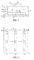
- Fig. 1 light from optical signal 20 is incident on sensing assembly 22.
- Ray 32 illustratively represents light in optical signal 20 that is incident on assembly 22, with ray 32 representing a spot 30 designated "S".
- IC 40 which includes photosensor array 42 with cell 44.
- Relative scanning movement between optical signal 20 and array 42 is illustrated by arrow 50, showing movement of ray 32 representing spot 30, and arrow 52, showing movement of assembly 22 including array 42.
- Spot S can include a distribution of photon energies resulting, for example, from a light source (not shown), an illuminated object, an optional optical component (not shown) between the illuminated object and array 42, or any other component that participates in production of optical signal 20.
- Light sources, illuminated objects, and optical components can be implemented in many ways. Potentially useful optical components include conventional imaging lenses (e.g. refractive lenses), diffractive optics (e.g. Fresnel lenses), various microlenses, and gradient index lenses (e.g. GRIN or Selfoc® lenses).
- Array 42 can obtain information about the distribution of photon energies in spot S because its cells photosense subranges of photon energies that vary laterally in the y-direction as illustrated by curve 60.
- the range of photon energies photosensed by array 42 is illustratively bounded by minimum and maximum wavelengths ⁇ min and ⁇ max , with curve 60 illustratively rising monotonically from ⁇ min at the leftmost cell in array 42 to ⁇ max at the rightmost cell in array 42, though the lateral variation could follow any appropriate function of position in the y-direction.
- Fig. 2 shows in more detail relative scanning movement of optical signal 20 across a series of positions on array 42 that are in a scan path of optical signal 20.
- Locations L m are examples of spots of an optical signal, as defined above, and each of locations L m can be treated as containing a distribution D m of photon energies in a given implementation; the distributions for locations L 1 through L M can therefore be referred to as D 1 through D M ..
- location is used here because it suggests that the spots of the optical signal are located relative to each other. As mentioned below, various measures can be taken to preserve resolution of an optical signal so that its locations or other spots remain distinct and are located in the same way.
- Each of the locations L 1 through L M is photosensed at a series of N positions on array 42, illustrated as Y 1 through Y N .
- each column of cells of array 42 includes subrange cells that photosense the same subrange of photon energies, but at a given position along the x-direction, each row of array 42 includes subrange cells that vary laterally from photon energies with wavelength ⁇ 1 through ⁇ N .
- all M positions in optical signal 44 are photosensed in a subrange centered on ⁇ n .
- each distribution D m in optical signal 44 is photosensed in each of the subranges centered on ⁇ 1 through ⁇ N .
- Locations L m play an important role in the technique of Figs. 1 and 2.
- the lower limit on size of locations L m constrains the resolution that can be obtained.
- spatial resolution of locations L m is limited by the effective area of cells in array 42.
- spectral resolution for each location L m depends on effective cell size in the y-direction and on the rate of change in ⁇ n across array 42; for example, if variation in ⁇ n results from variation in thickness of coating, spectral variation depends on the gradient or steepness of the coating surface.
- Relative scanning movement across a photosensor array with laterally varying subrange cells as in Figs. 1 and 2 makes it possible to obtain spectral information about optical signals.
- Subranges of photosensing are "different from each other" in a given application if, at the application's minimum photon proportion, the subranges produce distinguishable photosensing results when the application requires. For example, if two subranges are so similar that their photosensing results cannot be distinguished when required, they are not different from each other. It should be noted, however, that subranges that are different from each other can nonetheless overlap or one of them can include another.
- Fig. 3 is a schematic view of an exemplary implementation of lC 40 with photosensor array 42 that could be used in any of Figs. 4-9.
- Photosensor array 42 is illustratively a two-dimensional array, with at least two rows of cells that include photosensors.
- photosensor array 42 can be provided with different coatings or can be otherwise structured so that their cells photosense different ranges or subranges of photon energies.
- the information obtained from a single IC can provide a detailed analysis of incident photons over a broad range of photon energies.
- reference cells can be used to provide a spatially resolved real-time reference signal.
- a feature of array 42 is that it includes one or more reference cells that are nearby to a subrange cell.
- Each cell in row 102 photosenses photons throughout a suitable range, characterized as ⁇ all , to produce a reference for a nearby cell in row 104.
- ⁇ all a suitable range
- the cell in row 102 must be different from the cells in row 104.
- Each cell in row 104 photosenses a respective subrange between ⁇ min and ⁇ max , with illustrative cell 106 photosensing a subrange centered around ⁇ p .
- IC 40 also includes array circuitry as well as peripheral circuitry 110 which perform various functions relating to readout of photosensed information from array 42.
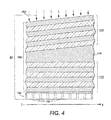
- Fig. 4 illustrates an implementation of assembly 22. Assembly 22 in Fig. 4 can be supported by a suitable support component.
- a cross-section has been taken through a fragment 150 of a photosensor array, with cells 152 of the fragment 150 shown schematically in cross-section. Over cells 152 is a transmission structure 160 that receives incident light 162.
- a structure that "transmits" photons is any material structure through which light can propagate. It is not necessary that there be a one-to-one relationship between photons that enter a transmission structure and photons that exit from it as long as the structure provides exiting photons in response to entering photons as a result of light propagation through the structure.
- to "transmit" photons is to perform a function by which exiting photons at an exit position are provided in response to entering photons at an entry position as a result of light propagation between the entry and exit positions.
- To “transmit only" a specified set of photons from a first position to a second refers to a function that transmits photons from the first position to the second, but predominantly photons in the specified set.
- a transmission structure transmits only a specified set of photons, between 60-90% of the transmitted photons are in the specified set, but the percentage could be lower or higher. In some applications, 90% or even 95% or more of the photons are in the specified set.
- One type of transmission structure is a "coating", meaning a layered structure of light-transmissive material that is on or over another component such as a photosensor array.
- a coating varies "continuously" along a scan path or other path if the coating varies as a continuous function of its position along the path.
- a transmission structure provides (and a cell receives from a transmission structure) photons "throughout", “within”, or “in” a range or subrange if the provided photons are predominantly within the range or subrange.
- photons typically have energies within the range or subrange, but the percentage could be lower or higher. In some applications, 90% or even 95% or more of the photons have energies within the range or subrange.
- Transmission structure 160 can be a film with laterally varying light transmission properties. In the portion of transmission structure 160 shown in Fig.4, wedge-shaped transmissive cavity 170 is enclosed between reflective films 172 and 174, forming a wedge-shaped Fabry-Perot etalon. Because its thickness varies as a function of position along the y-axis, transmission structure 160 will transmit different wavelengths as a function of position along the y-axis.
- Transmission structure 160 can be produced with appropriate coatings on or over a photosensor array.
- Films 172 and 174 and cavity 170 could all be produced by exposure to deposition beams in an evaporation chamber; uniform thicknesses could be produced by appropriate on-axis deposition, while laterally varying thickness can be produced by appropriate off-axis deposition.
- Fig. 4 illustratively shows films 172 and 174 as relatively thick compared to cavity 170, which would be appropriate for layers of non-metallic material such as SiO 2 , TiO 2 or Ta 2 O 5 . If films 172 and 174 are reflective metal, however, they could be much thinner.
- cavity 170 and films 172 and 174 could be designed from the desired transmitted wavelength ⁇ and the refractive index n of cavity 170.
- the thickness of cavity 170 is typically chosen to be ⁇ /(2n) or an integer multiple thereof, while the thicknesses of Bragg mirror layers within films 172 and 174 are typically ⁇ /(4n).
- the number of pairs of such layers in each of films 172 and 174 can vary between a few (e.g. 2-5) all the way up to 20 or 30, depending on the difference in refractive index between the two materials used, the desired transmission band width, and the desired stop band reflectivity, Therefore, in typical implementations, films 172 and 174 are much thicker than cavity 170.
- Fig. 5 illustrates the laterally varying light transmission properties of transmission structure 160. Because its thickness varies as a function of position along the y-axis, cavity 170 transmits different wavelengths as a function of position along the y-axis. Wavelengths of photons predominantly transmitted to nine of cells 152 as in fragment 150 are illustrated by the low reflectivity minima labeled 1 through 9. The high-transmissivity photon energy range for transmission structure 160 varies laterally.
- Fig. 6 illustrates another implementation of assembly 22.
- Assembly 22 includes transmission structure 180.
- Transmission structure 180 can be a laterally graded Bragg mirror in which each of layers 182, 184, 186, and 188 is laterally graded..
- Fig. 7 illustrates the laterally varying light transmission properties of transmission structure 180.
- Transmission structure 180 reflects different wavelengths as a function of position along the y-axis. Curves 200, 202, 204, and 206 are shown, representing reflectivity of the portion of transmission structure 180 over each of four cells 152 in fragment 150, with curve 200 being for the leftmost cell of the four in Fig. 6 and curve 206 being for the rightmost cell of the four.
- the high-reflectivity photon energy range for transmission structure 180 varies laterally.
- Fig. 8 illustrates a technique that produces transmission structure 210 with laterally varying light transmission properties similar to those illustrated in Figs. 5 and 7 but with lateral variation in each of two dimensions.
- Transmission structure 210 is produced on or over cells 152 of photosensor array 150 by using deposition source 212 to provide deposition beam 214 that can be characterized at any given point on the surface of structure 210 by two angles. One of the two angles results from angular variation of deposition beam 214 in the x-direction across array 150, while the other results from angular variation in the y-direction. As a result, the thickness gradient of structure 210 is similarly different in the x- and y-directions. Therefore, cells within each row extending in the y-direction will photosense a range of photon energies similarly to Fig. 7, but the range will be different than the range photosensed by cells in any other row extending in the same direction.
- Fig. 9 illustrates a technique that produces transmission structure 220 with laterally varying light transmission properties but without variation in thickness of transmission structure 220.
- the technique in Fig. 9 can be characterized as providing laterally varying optical thickness d*n, where d is thickness and n is index of refraction, but without actual variation in thickness d.
- homogeneous coating 222 is deposited by deposition source 224, which provides deposition beam 226 uniformly over the surface of photosensor array 150.
- light source 230 provides radiation 232 that is scanned across the coating over array 150 to introduce a laterally varying change of refractive index in resulting transmission structure 220.
- source 230 can be an ultraviolet source that provides intensity I with a constant value along each line parallel to the x-axis (perpendicular to the plane of Fig. 9), but varying from I min for lines nearer the x-axis to I max for lines farther from the x-axis.
- the wavelengths transmitted to cells in array 150 can vary along the y-axis from ⁇ min to ⁇ max , as shown.
- the same pattern of intensity can be concurrently applied by source 230 to each of a number of arrays that are appropriately arranged, allowing batch fabrication of arrays. Two-dimensional variation could also be obtained.
- spectral information about incident photons is obtained.
- nearby cells such as in a parallel row, can photosense quantities of photons throughout the range of photon energies to provide reference information. If adjacent cells in the array have overlapping subranges, computational techniques such as deconvolution can be used to improve accuracy.
- the resolution of a technique as in any of Figs. 4-9 depends heavily on the number of cells in an array, the full width half maximum (FWHM) of the transmission peak, and the peak shift per cell.
- the totally covered spectral width can be enhanced by increasing the FWHM and the peak shift per cell. Therefore, the technique can be customized to the needs of a specific application.
- the use of a Fabry-Perot cavity as in Fig. 4 enables very high spectral resolution, while a version with multiple cavities and many layers as in commercially available products will be favorable for applications with low light intensities in combination with small spectral resolution such as with fluorescence.
- the spectral width of the transmission window and the reflectivity of the stop band can be optimized separately, which may be advantageous because the reflectivity of the stop band determines stray light suppression. It would also be possible to use a single laterally graded distributed Bragg reflector (DBR) mirror as in Figs. 6 and 7 to obtain a photosensor array with high light sensitivity but limited wavelength resolution, appropriate for fluorescence or luminescence sensing.
- DBR distributed Bragg reflector
- the photocurrent in each cell is slightly different from its neighbors depending on the incident light spectrum. If the transmission properties of the DBR over each cell are known, the original spectrum of incident light can be reconstructed. The number of cells defines the number of spectral points that can be reconstructed and therefore determines spectral resolution. The reconstruction works best for wavelengths where transmission changes drastically from one cell to the next. Therefore, this technique could be used to resolve wavelengths at the edges of the DBR mirror.
- the DBR mirror could be positioned in such a way that the side edges on one side cover the spectral region being analyzed. Multiplication of the resulting photocurrent with a matrix that contains the transmission function of the DBR mirror provides a reconstruction of the incident light spectral distribution.
- Resolution can be improved by positioning DBRs on a second row of the photodiode array so that the opposite edge of the reflectivity plateau overlaps the spectral range of interest.
- lC 40 can be thought of as a chip-size spectrometer that includes a photosensor array together with a laterally varying filter such as a coating. The laterally varying transmission and reflection properties of the coating over the photosensor array define a correlation between position and photon energy. Therefore the spatially dependent signal from the photosensor array contains information about the incident spectrum. Because of the distributed nature of the spectrometer and the fact that the incident light traverses the photosensor array in the process of resolving spectral distribution, sensitivity is improved, making additional optics unnecessary.
- a coating as in Fig. 4 typically transmits approximately 60% of photons in its respective subrange.
- the subranges can be chosen with wavelengths that span between 0.01 and tens of nanometers (nm), depending on the design and gradient of the coating and the cell size of the photosensor array. Very high light yield can be achieved by using a highly sensitive photosensor.
- any coating or other transmission structure over row 102 in Fig. 3 must function as a gray filter across the range ⁇ all in order to provide a suitable reference, It may also be possible to leave row 102 uncoated in some implementations.
- Figs. 10-19 illustrate examples of how line-like and two-dimensional optical signals can be obtained from two-dimensional objects using various illumination techniques and optical components.
- Figs. 10-12 illustrate three implementations in which two-dimensional objects are illuminated in different ways to obtain optical signals.
- light from a source illuminates an object, resulting in the optical signal which may be a two-dimensional optical signal or a line-like optical signal.
- an optical signal that does not require illumination such as an externally available image like that ordinarily captured by a camera or an optical signal that results from self-fluorescence or from a form of excitation other than illumination.
- object 250 is illuminated by light from source 252, resulting in optical signal 254 due to reflection from object 250.
- Object 250 could be a sheet of paper or other sheet-like medium. More generally, object 250 could be any object with a two-dimensional surface that has varying reflectivity, such as a well-plate or a biochip, and optical signal 254 indicates reflectivity of the surface.
- fluid is used herein to encompass liquids, gasses, and aerosols.
- layer and channel are used herein with slightly different meanings:
- a "layer” of fluid is any thin liquid or aerosol layer that is captured within a carrier structure; for example, a glass slide's surface could hold a layer of fluid that contains analytes, and the fluid could in turn be covered by another glass slide or the like so that it is captured by surface tension effects.
- a “channel” is any tube or other enclosed passage that can contain fluid; for example, a channel can be defined in a "fluidic structure", meaning a structure that depends for its operation on fluid positioning or fluid flow.
- optical signal 274 results from transmission of light through object 270. Therefore, this configuration is appropriate for a well-plate, a biochip, or another two-dimensional object in which absorption, internal reflection, or another characteristic that affects light transmission varies from position to position. Optical signal 274 can therefore indicate absorption or internal reflection characteristics of object 270.
- object 290 is a waveguiding structure in which photons can emanate in response to illumination or other excitation, such as light from source 292.
- Object 290 could, for example, be a biochip with fluid within or adjacent to waveguides or with non-fluid particles adjacent to waveguides.
- illumination or other excitation analytes or other particles within object 290 fluoresce, providing optical signal 294.
- Optical signal 294 therefore indicates differences between fluorescence spectra at different positions within object 290.
- biochips and other two-dimensional objects can be implemented with illumination or other excitation techniques that cause fluorescence.
- Enhanced light-target interaction is especially important in characterizing single particles or low concentrations of biological or chemical agents.
- Anti-resonant waveguide techniques can improve the interaction because of the extended length in which interaction occurs. More particularly, in contrast to excitation techniques that use evanescent fields of ordinary waveguides and therefore require very small channels, fluidic channels with maximum transverse dimensions as great as a few millimeters can be used as anti-resonant waveguides.
- Suitable anti-resonant waveguide configurations can include an aerosol in a glass capillary tube or a liquid film between glass slides. The excitation could be with appropriate electromagnetic radiation.
- an analyte within object 290 fluoresces, emitting light with a characteristic spectrum of photon energies. A portion of the light is emitted toward assembly 22, becoming part of optical signal 294. After possibly passing through an optical component, photons can therefore be photosensed by cells of photosensor array 42 on IC 40.
- the resulting optical signals 254, 274, and 294 could thus be provided to assembly 22 through an optical component, which may not be necessary in some implementations.
- a two-dimensional object is illuminated with a very thin line, and secondary relative scanning movement can be performed between the illumination and the object to obtain optical signals from all parts of the object; in these examples, the thickness of the illuminating line determines the spatial resolution in a y-direction, while an optical component preserves resolution in an x-direction.
- a two-dimensional optical signal is received from the object, and an optical component converts it to a line-like optical signal or to a two-dimensional optical signal that can be scanned across a photosensor array in assembly 22.
- Illumination and optical techniques to obtain line-like optical signals generally fall into either of two basic possibilities.
- One of these possibilities uses “line-like illumination”, meaning illumination approximating a line, while the other uses a “line-like aperture”, meaning an aperture approximating a line.
- the size of an illuminated field defines the size of the resulting optical signal and an optical component preserves resolution in the direction of the line.
- a very thin line of illumination may be necessary to obtain a desired spatial resolution in the y-direction while an optical component preserves resolution in the x-direction.
- a secondary scanning device can be used to produce relative movement between a combination of illumination and optical components and an object being illuminated in order to cover the whole object.
- an illuminated field is larger than the desired optical signal, and an optical component provides both a line-like aperture, and a structure that preserves resolution in the x-direction.
- a secondary scanning device can produce relative movement, in this case either between the illuminated field and an optical component or between the illuminated object and a combination of illumination and optical components.
- Techniques to obtain two-dimensional optical signals by illuminating two-dimensional objects generally use a lens or lens-like optical component to preserve resolution in both x- and y-directions.
- the optical components can be used to image the illuminated object onto a two-dimensional photosensor array.
- each specific illuminated location in the y-direction of the object is imaged onto a specific location in the y-direction of the array.
- Primary relative scanning movement can be obtained by moving the object in approximately the y-direction relative to a combination of illumination, optical, and sensing components, enabling photosensing of a series of subranges for each location,
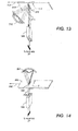
- Fig. 13 illustrates an example in which sheet 310 of paper or another suitable sheet-like medium bears an image on its lower side and is illuminated from its lower side by source 312, which could be a white LED array with appropriate optics.
- source 312 which could be a white LED array with appropriate optics.
- a line-like optical signal 314 similar to optical signal 20 in Fig. 2
- Line-like optical signal 314 is then transmitted through an optical component such as Selfoc® lens array 320 to preserve resolution in the x-direction. From array 320, the optical signal can be transmitted to assembly 22.
- a series of line-like optical signals similar to signal 314 must be obtained, such as by secondary relative scanning movement or other relative movement between source 312 and sheet 310, as suggested by arrow 322.
- Fig. 14 shows object 350, which can be an array that presents results of biological or chemical analysis in optical form, such as a 96-well-plate for analyzing biological or chemical samples.
- Object 350 could be illuminated from its backside by source 352, as shown, or alternatively could be illuminated from its front side.
- a line-like optical signal 354 can be produced from a line-like segment 356 of plate 350.
- Signal 354 is transmitted through Selfoc® lens array 320 and thence to assembly 22.
- a complete image can be obtained, such as by secondary relative scanning movement or other relative movement between source 352 and object 350, as suggested by arrow 360.
- object 400 is illuminated in any of the ways described above in relation to Figs. 10-12, providing two-dimensional optical signal 402.
- Optical component 404 illustratively includes both a two-dimensional light-blocking layer 410 with slit 412, and also Selfoc® lens array 420, similar to array 320 in Figs. 13 and 14. Relative scanning movement or other relative movement between object 400 and component 404, as suggested by arrow 422, results in a series of line-like optical signals 424, each extending in the x-direction, with array 420 preserving resolution in the x-direction.
- Figs. 13-15 could also be implemented to obtain optical signals that emanate from a point-like source.
- object 450 is illuminated to produce two-dimensional optical signal 452.
- An optical component is implemented in this case as a conventional lens 460 and is positioned such that it produces a sharp image of illuminated object 450 on photosensor array 42 in assembly 22.
- Light in optical signal 452 is focused so that individual illuminated locations of object 450 are photosensed at respective locations of array 42, resulting in photosensing different energy subranges at different locations.
- Object 450 can be imaged one-to-one onto array 42 by positioning both object 450 and array 42 at twice the focal length of lens 460.
- a conventional lens like lens 460 would ordinarily have to be bigger than the object being imaged.
- Replacing lens 460 by a Selfoc® or GRIN lens avoids this problem.
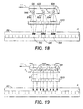
- object 500 is illuminated to produce two-dimensional optical signal 502.
- an optical component is implemented as a two-dimensional Selfoc® lens array 510, producing approximately the same optical result as in Fig. 16.
- Fig. 18 shows a detail from one implementation as in Fig. 17.
- Object 500 is illuminated to produce a two-dimensional optical signal.
- Two-dimensional Selfoc® lens array 510 images object 500 onto array 42 in sensing assembly 22.
- Locations 520, 522, and 524 emanate photons, represented respectively by ray groups 530, 532, and 534; the photons may result from reflection, transmission, or fluorescence.
- ray groups 530, 532, and 534 are photosensed by cells 540, 542, and 544, respectively. Quantities read out from cells of array 42 can be used to obtain spectra! information about locations 520, 522, and 524 even though all three locations are concurrently traveling past array 42.
- Fig. 19 shows an alternative to the implementation in Fig. 18.
- Object 500 includes a continuous sequence of closely spaced locations moving through the illuminated field.
- Fig. 19 shows a group of the locations passing through the illuminated field, led by location 560, after which follow several intermediate locations 562 and, finally, location 564.
- Locations 560, 562, and 564 emanate photons, represented by rays 570, such as by reflection, transmission, or fluorescence, and the photons pass through Selfoc® lens array 510 so that, for each of locations 560, 562, and 564, emanating photons are predominantly incident on a different cell of array 42 than photons emanating from other nearby locations.
- Quantities read out from cells of array 42 can be used to obtain spectral information about locations 560, 562, and 564 even though a continuous sequence of closely spaced locations is concurrently traveling past array 42.
- Fig. 20 illustrates features of a system in which relative scanning motion occurs.
- System 600 is an exemplary system that could be used to obtain spectral information using photosensing with relative scanning movement.
- System 600 illustratively includes central processing unit (CPU) 602 connected to various components through bus 604, but a wide variety of other architectures could be employed
- System 600 also includes external input/output (l/O) component 606 and memory 608, both connected to bus 604.
- External I/O 606 permits CPU 602 to communicate with devices outside of system 600.
- external I/O 606 could be connected to a suitable user interface, such as a monitor and keyboard.
- Additional components connected to bus 604 are within or connected to system 600.
- lC I/O 610 permits CPU 602 to communicate with M ICs, illustrated by a series from lC(0) 612 to lC(M-1) 614, including lC(m) 616 with a photosensor array 618.
- scanning device I/O 620 permits CPU 602 to communicate with various devices to produce relative scanning movement, such as motors and sensors; N scanning devices are represented in Fig. 20 by device (0) 622 through device (N-1) 624.
- Memory 608 includes program memory 630.
- the routines stored in program memory 630 include scanning routine 640 and readout and combine routine 642.
- CPU 602 executes scanning routine 640 to communicate with scanning devices 622 through 624.
- CPU 602 can receive signals from sensors, perform computations to determine what movements are necessary to obtain a desired scanning motion, and then provide signals to activate motors to produce appropriate relative movement of an optical signal with respect to array 42.
- CPU 602 can provide signals to each of ICs 612 through 614 to read out subrange cells and to store the photosensed quantities for each spot or other distinguishable part of an optical signal with quantities for each spot or other part of the optical signal combined in an appropriate data structure (not shown), such as by forming a data array or list.
- CEach location L m would have a distribution of photon energies D m , which could be closely approximated by spectral information from the photosensed quantities in different subranges. A high readout rate with short sensing periods may be necessary to obtain satisfactory resolution.
- CPU 602 can provide them through external I/O 606.
- all of the photosensed quantities for an entire illuminated field could be combined into a single data structure and provided through external I/O 606 through a suitable streaming operation.
- System 600 could be implemented with any scanning devices that produce relative scanning motion.
- Figs. 21-23 illustrate several exemplary types of applications using different scanning techniques, any of which could be implemented with system 600 as in Fig. 20.
- Fig. 21 shows apparatus 700, an example of a type of application in which a point-like or line-like optical signal obtained by illuminating an object follows a scan path across array 42 (Fig. 1) in assembly 22.
- Outer scanning device 702 produces secondary relative scanning movement through motion of one or both of support components 704 and 706.
- Support component 704 supports object 710, which could be a sheet of paper, a biochip, or a well plate.
- Support component 706 supports inner scanning assembly 712, which in turn includes inner scanning device 720.
- Inner scanning device 720 produces primary relative scanning movement through motion of one or both of support components 722 and 724.
- Support component 722 supports optical signal assembly 730, a group of components that must move in a coordinated manner to provide a suitable optical signal.
- support component 724 supports sensing assembly 22.
- illumination source 732 illustratively provides point-like or line-like illumination to produce a point-like or line-like optical signal through reflection.
- optical component 734 illustratively preserves x-direction resolution of the optical signal during primary relative scanning movement with respect to array 42 (Fig. 1), and can include an array as in Fig. 13.
- Apparatus 700 illustrates a type of application in which scanning device 702 provides scanning of all locations of object 710 while scanning device 720 provides scanning of all photon energy subranges for each location of object 710.
- scanning routine 640 in Fig. 20 could provide signals in various ways.
- Device 702 could be controlled to obtain an optical signal from each of a series of locations and, for each location in the series, device 720 could be controlled to produce relative scanning movement of the optical signal across array 42.
- device 720 could be controlled to again produce primary relative scanning movement, providing the optical signal to each of a series of sets of subrange cells in array 42; for each set of cells, device 702 could be controlled to scan all locations of object 710 across each successive set of cells.
- Fig. 22 shows apparatus 750, an example of another type of application in which a two-dimensional optical signal obtained by illuminating an object follows a scan path across array 42 (Fig. 1) in assembly 22.
- the illustrated implementation includes only one scanning device, device 752, which produces relative scanning movement through motion of one or both of support components 754 and 756.
- Support component 754 supports object 760, which could be a sheet of paper, a biochip, or a well plate.
- Support component 756 supports scanning and sensing assembly 762, a group of components that must move in a coordinated manner to provide appropriate relative scanning movement.
- illumination source 764 illustratively illuminates a two-dimensional field that includes most or all of the lower surface of object 760, producing a two-dimensional optical signal through reflection.
- Optical component 766 preserves both x- and y-direction resolution of the optical signal during relative scanning movement with respect to array 42 in sensing assembly 22, which is also included in assembly 762.
- scanning routine 640 in Fig. 20 could control device 752 to produce relative scanning movement so that the optical signal follows an appropriate scan path across array 42.
- Readout and combine routine 642 could read out photosensed quantities of photons at a series of positions along the scan path and, based on scanning speed, could then combine photosensed quantities that indicate spectral information for the same location on object 760 in an appropriate data structure.
- Fig. 23 shows apparatus 800 in which a two-dimensional optical signal obtained in any suitable way follows a scan path across array 42 (Fig. 1) in assembly 22.
- the illustrated implementation includes only one scanning device, device 802, which produces relative scanning movement through motion of one or both of support components 804 and 806.
- Support component 804 supports optical assembly 810, a group of components that must move in a coordinated manner to provide appropriate relative scanning movement.
- support component 806 supports sensing assembly 22.
- optical signal source 812 can be any source of an optical signal that includes spectral information.
- Signal source 812 could include a light source that illuminates a surface or one or more stationary or slow-moving objects in any of the ways shown in Figs. 10-12, or could be an aperture or other appropriate optical component for receiving an external optical signal into optical assembly 810.
- Optical component 814 can preserve both x- and y-direction resolution of the optical signal during relative scanning movement with respect to array 42 in sensing assembly 22. Unlike scanning and sensing component 762 in Fig. 22, however, optical signal assembly 810 does not include sensing assembly 22, and relative scanning movement can therefore occur between assemblies 810 and 22.
- Optical signal assembly 810 could always be held fixed relative to scanning device 802, such as in a camera application, so that relative scanning movement is accomplished entirely by movement of assembly 22 relative to scanning device 802.
- the various support components are illustratively shown as cantilevered from scanning devices, but support components could generally be implemented with any suitable sizes, shapes, and materials, and could be connected to and controlled by scanning devices in any suitable way.
- support components could be connected directly or indirectly to the components they support in any appropriate way and could, where appropriate, support an object on a platen or in another suitable way during scanning.
- relative scanning motion could be accomplished through one or both support components, meaning that, in a specific application, one support component could be stationary.
- the exemplary implementations described above can provide compact, inexpensive components to perform functions such as spectrometry of optical signals, and can achieve high spatial and spectral resolution.
- the techniques can be implemented in existing scanners and printers, including those available in the consumer market.
- the results of photosensing can be read out rapidly and in parallel from a number of lCs.
- a number of lCs may be used to address a wide range of photon energies by using suitable coating materials, possibly ranging from the ultraviolet to the far infrared and even into the terahertz range.
- Scanning implementations as described above can be applied in various imaging applications, such as document scanners or copiers and digital cameras. Scanning implementations as described above can also be applied in spectrophotometers and other spectroscopic applications for color control or process control or in parallel readout of optical sensors such as two-dimensional photonic crystal sensors or biosensors, whether performing spectroscopy of solids such as semiconductor materials or liquids or aerosols that include bio-particles or other analytes. Relative movement could be obtained in various ways other than scanning. Photosensor arrays and sources of optical signals could be in various other configurations.
- the exemplary implementations described above generally rely on transmission structures that include highly reflective interfaces, so that much of the incident light is reflected and only a small fraction reaches the photosensor array. Therefore, the techniques described above are especially useful in applications in which light intensity is very high or a light source emits through a large area or over an extended time. In addition, the above techniques make it possible to increase sensitivity by choosing very long integration times (without loss of throughput capacity), simpler optics, and no dispersion element. By contrast, some conventional systems such as monochromators lose all light diffracted into the 0 th , 2 nd , and higher orders. In the implementations described above, very high light yield can be achieved by combining a transmission structure with a highly sensitive photosensor array, such as one that includes avalanche photodetectors.
- Components could have other various shapes, dimensions, or other numerical or qualitative characteristics.
- Some of the above exemplary implementations involve specific materials, such as in photosensor arrays and transmission structures, but a wide variety of materials could be used with layered structures with various combinations of sublayers.
- Some of the above exemplary implementations employ waveguiding techniques to obtain fluorescence.
- the techniques described above could also be used for self-emitting or auto-fluorescing objects such as particles.
- Various types of fluorescence, photo-luminescence, chemo-fluorescence, inelastic scattering, etc.could be employed.
- the technique of anti-resonant waveguiding is only one of many waveguiding techniques that could be used continuously or intermittently. Various parameters could be adjusted to obtain anti-resonant waveguiding.
- a CPU which could be a microprocessor or any other appropriate component.
Abstract
Description
- The present invention relates to photosensing photon energies of optical signals with photosensor arrays on integrated circuits (ICs).
-
U.S. Patent No. 5,186,755 describes a spectrometer apparatus in which a spectrum resolving sensor contains an opto-electronic monolithic array of photosensitive elements and a continuous variable optical filter. - It would be advantageous to have improved techniques for photosensing optical signals with lCs.
- In accordance with a first aspect of the present invention, a method of sensing optical signals comprises causing relative scanning movement between an optical signal and a photosensor array included in an lC, the optical signal including photons within an application's range of photon energies; the optical signal following a scan path across the array along which cells in the array photosense photons in the optical signal; and
in each of two or more segments of the scan path, using a respective set of one or more cells in the array to photosense quantities of photons in the optical signal; each segment's respective set of cells photosensing photons within a respective subrange of the range of photon energies; the respective subranges of at least two of the segments being different from each other. - In accordance with a second aspect of the present invention, apparatus comprises an IC that includes a photosensor array; the array including cells that photosense quantities of photons received; and
a scanning device that produces relative scanning movement between an optical signal and the photosensor array, the optical signal including photons within an application's range of photon energies; the optical signal following a scan path across the array along which cells in the array photosense photons in the optical signal; in each of two or more segments of the scan path, a respective set of one or more cells in the array photosensing quantities of photons in the optical signal; each segment's respective set of cells photosensing photons within a respective subrange of the range of photon energies; the respective subranges of at least two of the segments being different from each other. - These and other features and advantages of exemplary embodiments of the invention are described below with reference to the accompanying drawings.
- Fig. 1 is a schematic diagram illustrating relative scanning movement between an optical signal and a photosensor array in a sensing assembly.
- Fig. 2 is a schematic top view of a line-like optical signal in scanning movement relative to a photosensor array in Fig. 1.
- Fig. 3 is a schematic plan view of an implementation of an assembly that can be used in Fig. 1.
- Fig. 4 is a schematic cross-sectional view of another implementation of an assembly that can be used in Fig. 1.
- Fig. 5 is a graph illustrating laterally varying light transmission properties of a transmission structure in Fig. 4.
- Fig. 6 is a schematic cross-sectional view of another implementation of an assembly that can be used in Fig. 1.
- Fig. 7 is a graph illustrating the laterally varying light transmission properties of a transmission structure in Fig. 6.
- Fig. 8 illustrates a technique that produces a transmission structure that can be used in an assembly as in Fig. 1.
- Fig. 9 illustrates another technique for producing a transmission structure that can be used in an assembly in Fig. 1.
- Fig. 10 is a schematic perspective view showing how a line-like optical signal could be obtained using a two-dimensional object such as a sheet of paper.
- Fig. 11 is a schematic perspective view showing how a line-like optical signal could be obtained by illuminating a two-dimensional object such as a 96-well array.
- Fig. 12 is a schematic perspective view showing another way in which a line-like optical signal could be obtained by illuminating a two-dimensional object such as a biochip.
- Fig. 13 is a schematic perspective view illustrating an illumination technique and an optical component that can be used to obtain a line-like optical signal.
- Fig. 14 is a schematic perspective view illustrating an alternative combination of an illumination technique with an optical component to obtain a line-like optical signal.
- Fig. 15 is a schematic partially perspective view illustrating an optical component that can be used to obtain a line-like optical signal from a two-dimensional optical signal.
- Fig. 16 is a schematic partially perspective view illustrating an optical component that can be used to focus a two-dimensional optical signal on a sensing assembly as in Fig. 2.
- Fig. 17 is a schematic partially perspective view illustrating an alternative optical component that can be used in place of the optical component in Fig. 16.
- Fig. 18 is a schematic partially perspective view illustrating in greater detail an implementation of the technique in Fig. 17.
- Fig. 19 is a schematic partially perspective view illustrating in greater detail another implementation of the technique in Fig. 17.
- Fig. 20 is a schematic block diagram of a system that could control relative scanning movement as in Fig. 1.
- Fig. 21 is a schematic diagram of apparatus with outer and inner scanning devices, in which the outer scanning device can produce relative scanning movement as in Fig. 1.
- Fig. 22 is a schematic diagram of another apparatus that can produce relative scanning movement as in Fig. 1.
- Fig. 23 is a schematic diagram of another apparatus that can produce relative scanning movement as in Fig. 1.
- In this specification, "Light" refers herein to electromagnetic radiation of any wavelength or frequency; unless otherwise indicated, a specific value for light wavelength or frequency is that of light propagating through vacuum. The term "photon" refers herein to a quantum of light, and the term "photon energy" refers herein to the energy of a photon.
- The various exemplary implementations described below address problems that arise in obtaining information about light. One of those problems is the difficulty of obtaining spectral information about an optical signal rapidly and without bulky, expensive equipment. Also, techniques in obtaining spectral information about a document or other two-dimensional object have poor spectral resolution.
- The term "optical signal" is used herein to refer to a signal in the form of light. For example, an optical signal may "emanate from a point-like source", meaning that the light behaves as if its source were a point or had a very small area; for example, the light could be emitted or scattered by a particle or a compact group of particles. In contrast, a "line-like optical signal" is an optical signal that could be approximated by a straight line of point-like sources; illuminating a slit can produce a line-like optical signal, for example. A "two-dimensional optical signal" is an optical signal that could be approximated by a two-dimensional array of point-like sources; illuminating a two-dimensional object can produce a two-dimensional optical signal, for example.
- Optical signals can also be described in terms of "spots", where a "spot" of an optical signal refers to an area of the signal that can be approximated by an optical signal emanating from a point-like source. If a line-like or two-dimensional optical signal is produced by illuminating a two-dimensional object, for example, a "spot" of the optical signal would emanate from a single position on the object's surface.
- Some of the photosensing implementations described herein employ structures with one or more dimensions smaller than 1 mm, and various techniques have been proposed for producing such structures. In particular, some techniques for producing such structures are referred to as "microfabrication." Examples of microfabrication include various techniques for depositing materials such as growth of epitaxial material sputter deposition, evaporation techniques, plating techniques, spin coating, printing, and other such techniques; techniques for patterning materials, such as etching or otherwise removing exposed regions of thin films through a photolithographically patterned resist layer or other patterned layer; techniques for polishing, planarizing, or otherwise modifying exposed surfaces of materials; and so forth.
- An "integrated circuit" or "IC" is a structure with electrical components and connections produced by microfabrication or similar processes. An lC may, for example, be on or over a substrate on which it was produced or another suitable support structure. Other components could be on the same support structure with an lC, such as discrete components produced by other types of processes.
- Figs. 1 and 2 illustrate general features of relative scanning movement. Figs. 3-9 illustrate features of ICs and sensing assemblies that can be used as in Figs. 1 and 2. "Relative movement" or "relative motion" occurs between an optical signal and a photosensor array when there is a change in the position at which at least one spot of the optical signal is incident on the array. In general, relative motion between an optical signal and an array can result from motion of the array, motion of one or more of the components that provide the optical signal, or motion both of the array and of one or more of the components that provide the optical signal.
- Sheets of paper are examples of "two-dimensional objects", meaning objects that have extent in at least two orthogonal directions. Other examples include biochips and well-plates, as mentioned below. In contrast to these other examples, a sheet of paper is also an example of a "sheet-like medium", meaning a two-dimensional object that is very thin in a third orthogonal direction, like a sheet, and that can be used as a medium for transfer of information.
- "Relative scanning movement" or "relative scanning motion" between an optical signal and another component refers to relative movement in which a spot of the optical signal follows a path, such as a path across an array, across a two-dimensional object, or across an optical component.
- In Fig. 1, light from
optical signal 20 is incident onsensing assembly 22. Ray 32 illustratively represents light inoptical signal 20 that is incident onassembly 22, withray 32 representing aspot 30 designated "S". Withinassembly 22, light fromspot 30 is incident on IC 40, which includesphotosensor array 42 withcell 44. Relative scanning movement betweenoptical signal 20 andarray 42 is illustrated byarrow 50, showing movement ofray 32 representingspot 30, andarrow 52, showing movement ofassembly 22 includingarray 42. - Spot S can include a distribution of photon energies resulting, for example, from a light source (not shown), an illuminated object, an optional optical component (not shown) between the illuminated object and
array 42, or any other component that participates in production ofoptical signal 20. Light sources, illuminated objects, and optical components can be implemented in many ways. Potentially useful optical components include conventional imaging lenses (e.g. refractive lenses), diffractive optics (e.g. Fresnel lenses), various microlenses, and gradient index lenses (e.g. GRIN or Selfoc® lenses). -
Array 42 can obtain information about the distribution of photon energies in spot S because its cells photosense subranges of photon energies that vary laterally in the y-direction as illustrated bycurve 60. The range of photon energies photosensed byarray 42 is illustratively bounded by minimum and maximum wavelengths λmin and λmax, withcurve 60 illustratively rising monotonically from λmin at the leftmost cell inarray 42 to λmax at the rightmost cell inarray 42, though the lateral variation could follow any appropriate function of position in the y-direction. - Fig. 2 shows in more detail relative scanning movement of
optical signal 20 across a series of positions onarray 42 that are in a scan path ofoptical signal 20.Optical signal 20 is illustratively a line-like optical signal extending in the x-direction, approximately perpendicular to its y-direction scan path acrossarray 42, and is illustrated as including M discrete parts or locations L1 through LM, with each location Lm being analogous to an image pixel; in the limiting case of M=1,optical signal 20 is a point-like optical signal that includes only one discrete location, L1. ln other cases,optical signal 20 can be two-dimensional, in which case it could be treated as a series of adjacent line-like optical signals each of which includes locations as shown in Fig. 2, extends in the x-direction, and moves acrossarray 42 in the y-direction, likeoptical signal 20. - Locations Lm are examples of spots of an optical signal, as defined above, and each of locations Lm can be treated as containing a distribution Dm of photon energies in a given implementation; the distributions for locations L1 through LM can therefore be referred to as D1 through DM.. The term "location" is used here because it suggests that the spots of the optical signal are located relative to each other. As mentioned below, various measures can be taken to preserve resolution of an optical signal so that its locations or other spots remain distinct and are located in the same way. As will be understood more fully from the below description of implementations with line-like or two-dimensional optical signals, it is advantageous to prevent the signal from spreading in the direction of relative movement, referred to generally herein as the y-direction; in other words, it is advantageous to keep the light of the optical signal concentrated such that each spot's light stays within the sensing area of a subrange cell.
- Each of the locations L1 through LM is photosensed at a series of N positions on
array 42, illustrated as Y1 through YN. At a given position along the y-direction, each column of cells ofarray 42 includes subrange cells that photosense the same subrange of photon energies, but at a given position along the x-direction, each row ofarray 42 includes subrange cells that vary laterally from photon energies with wavelength λ1 through λN. ln other words, at position Yn, all M positions inoptical signal 44 are photosensed in a subrange centered on λn. Similarly, in scanning between position Y1 and YN, each distribution Dm inoptical signal 44 is photosensed in each of the subranges centered on λ1 through λN. - Locations Lm play an important role in the technique of Figs. 1 and 2. The lower limit on size of locations Lm constrains the resolution that can be obtained. In general, spatial resolution of locations Lm is limited by the effective area of cells in
array 42. Similarly, spectral resolution for each location Lm depends on effective cell size in the y-direction and on the rate of change in λn acrossarray 42; for example, if variation in λn results from variation in thickness of coating, spectral variation depends on the gradient or steepness of the coating surface. - Relative scanning movement across a photosensor array with laterally varying subrange cells as in Figs. 1 and 2 makes it possible to obtain spectral information about optical signals. By choosing suitable materials in certain components, it is possible to obtain spectral information for the entire range from the deep ultraviolet to the far infrared or even for frequencies in the THz range.
- Subranges of photosensing are "different from each other" in a given application if, at the application's minimum photon proportion, the subranges produce distinguishable photosensing results when the application requires. For example, if two subranges are so similar that their photosensing results cannot be distinguished when required, they are not different from each other. It should be noted, however, that subranges that are different from each other can nonetheless overlap or one of them can include another.
- Fig. 3 is a schematic view of an exemplary implementation of
lC 40 withphotosensor array 42 that could be used in any of Figs. 4-9.Photosensor array 42 is illustratively a two-dimensional array, with at least two rows of cells that include photosensors. - Different rows or other parts of
photosensor array 42 can be provided with different coatings or can be otherwise structured so that their cells photosense different ranges or subranges of photon energies. As a result, the information obtained from a single IC can provide a detailed analysis of incident photons over a broad range of photon energies. In addition, reference cells can be used to provide a spatially resolved real-time reference signal. - A feature of
array 42 is that it includes one or more reference cells that are nearby to a subrange cell. - Each cell in
row 102 photosenses photons throughout a suitable range, characterized as λall, to produce a reference for a nearby cell inrow 104. For implementations in which it is advantageous to have signal strengths of the same order from a cell inrow 102 and its paired cell inrow 104, the cell inrow 102 must be different from the cells inrow 104. - Each cell in
row 104, on the other hand, photosenses a respective subrange between λmin and λmax, withillustrative cell 106 photosensing a subrange centered around λp.IC 40 also includes array circuitry as well asperipheral circuitry 110 which perform various functions relating to readout of photosensed information fromarray 42. - Fig. 4 illustrates an implementation of
assembly 22.Assembly 22 in Fig. 4 can be supported by a suitable support component. - In Fig. 4, a cross-section has been taken through a
fragment 150 of a photosensor array, withcells 152 of thefragment 150 shown schematically in cross-section. Overcells 152 is atransmission structure 160 that receivesincident light 162. - A structure that "transmits" photons, sometimes referred to herein as a "transmission structure", is any material structure through which light can propagate. It is not necessary that there be a one-to-one relationship between photons that enter a transmission structure and photons that exit from it as long as the structure provides exiting photons in response to entering photons as a result of light propagation through the structure.
- More generally, to "transmit" photons is to perform a function by which exiting photons at an exit position are provided in response to entering photons at an entry position as a result of light propagation between the entry and exit positions. To "transmit only" a specified set of photons from a first position to a second refers to a function that transmits photons from the first position to the second, but predominantly photons in the specified set. As with photosensing, described above, if a transmission structure transmits only a specified set of photons, between 60-90% of the transmitted photons are in the specified set, but the percentage could be lower or higher. In some applications, 90% or even 95% or more of the photons are in the specified set.
- One type of transmission structure is a "coating", meaning a layered structure of light-transmissive material that is on or over another component such as a photosensor array. A coating varies "continuously" along a scan path or other path if the coating varies as a continuous function of its position along the path.
- A transmission structure provides (and a cell receives from a transmission structure) photons "throughout", "within", or "in" a range or subrange if the provided photons are predominantly within the range or subrange. As with photosensing, described above, between 60-90% of the photons from a transmission structure typically have energies within the range or subrange, but the percentage could be lower or higher. In some applications, 90% or even 95% or more of the photons have energies within the range or subrange.
-
Transmission structure 160 can be a film with laterally varying light transmission properties. In the portion oftransmission structure 160 shown in Fig.4, wedge-shapedtransmissive cavity 170 is enclosed betweenreflective films transmission structure 160 will transmit different wavelengths as a function of position along the y-axis. -
Transmission structure 160 can be produced with appropriate coatings on or over a photosensor array.Films cavity 170 could all be produced by exposure to deposition beams in an evaporation chamber; uniform thicknesses could be produced by appropriate on-axis deposition, while laterally varying thickness can be produced by appropriate off-axis deposition. Fig. 4 illustratively showsfilms cavity 170, which would be appropriate for layers of non-metallic material such as SiO2, TiO2 or Ta2O5. Iffilms - Specific thicknesses of
cavity 170 andfilms cavity 170. The thickness ofcavity 170 is typically chosen to be λ/(2n) or an integer multiple thereof, while the thicknesses of Bragg mirror layers withinfilms films films cavity 170. - Fig. 5 illustrates the laterally varying light transmission properties of
transmission structure 160. Because its thickness varies as a function of position along the y-axis,cavity 170 transmits different wavelengths as a function of position along the y-axis. Wavelengths of photons predominantly transmitted to nine ofcells 152 as infragment 150 are illustrated by the low reflectivity minima labeled 1 through 9. The high-transmissivity photon energy range fortransmission structure 160 varies laterally. - Fig. 6 illustrates another implementation of
assembly 22.Assembly 22 includestransmission structure 180.Transmission structure 180 can be a laterally graded Bragg mirror in which each oflayers - Fig. 7 illustrates the laterally varying light transmission properties of
transmission structure 180.Transmission structure 180 reflects different wavelengths as a function of position along the y-axis.Curves transmission structure 180 over each of fourcells 152 infragment 150, withcurve 200 being for the leftmost cell of the four in Fig. 6 andcurve 206 being for the rightmost cell of the four. The high-reflectivity photon energy range fortransmission structure 180 varies laterally. - Fig. 8 illustrates a technique that produces
transmission structure 210 with laterally varying light transmission properties similar to those illustrated in Figs. 5 and 7 but with lateral variation in each of two dimensions. -
Transmission structure 210 is produced on or overcells 152 ofphotosensor array 150 by usingdeposition source 212 to providedeposition beam 214 that can be characterized at any given point on the surface ofstructure 210 by two angles. One of the two angles results from angular variation ofdeposition beam 214 in the x-direction acrossarray 150, while the other results from angular variation in the y-direction. As a result, the thickness gradient ofstructure 210 is similarly different in the x- and y-directions. Therefore, cells within each row extending in the y-direction will photosense a range of photon energies similarly to Fig. 7, but the range will be different than the range photosensed by cells in any other row extending in the same direction. - Fig. 9 illustrates a technique that produces
transmission structure 220 with laterally varying light transmission properties but without variation in thickness oftransmission structure 220. The technique in Fig. 9 can be characterized as providing laterally varying optical thickness d*n, where d is thickness and n is index of refraction, but without actual variation in thickness d. - In the upper part of Fig. 9,
homogeneous coating 222 is deposited bydeposition source 224, which providesdeposition beam 226 uniformly over the surface ofphotosensor array 150. - Then, in the lower part of Fig. 9,
light source 230 providesradiation 232 that is scanned across the coating overarray 150 to introduce a laterally varying change of refractive index in resultingtransmission structure 220. For example,source 230 can be an ultraviolet source that provides intensity I with a constant value along each line parallel to the x-axis (perpendicular to the plane of Fig. 9), but varying from Imin for lines nearer the x-axis to Imax for lines farther from the x-axis. As a result, the wavelengths transmitted to cells inarray 150 can vary along the y-axis from λmin to λmax, as shown. The same pattern of intensity can be concurrently applied bysource 230 to each of a number of arrays that are appropriately arranged, allowing batch fabrication of arrays. Two-dimensional variation could also be obtained. - If quantities photosensed by the cells are read out in parallel, spectral information about incident photons is obtained. As illustrated in Fig. 3, nearby cells, such as in a parallel row, can photosense quantities of photons throughout the range of photon energies to provide reference information. If adjacent cells in the array have overlapping subranges, computational techniques such as deconvolution can be used to improve accuracy.
- In general, the resolution of a technique as in any of Figs. 4-9 depends heavily on the number of cells in an array, the full width half maximum (FWHM) of the transmission peak, and the peak shift per cell. The smaller the FWHM and the peak shift, the better the resolution. On the other hand, the totally covered spectral width can be enhanced by increasing the FWHM and the peak shift per cell. Therefore, the technique can be customized to the needs of a specific application. For example, the use of a Fabry-Perot cavity as in Fig. 4 enables very high spectral resolution, while a version with multiple cavities and many layers as in commercially available products will be favorable for applications with low light intensities in combination with small spectral resolution such as with fluorescence. With such an approach, the spectral width of the transmission window and the reflectivity of the stop band can be optimized separately, which may be advantageous because the reflectivity of the stop band determines stray light suppression. It would also be possible to use a single laterally graded distributed Bragg reflector (DBR) mirror as in Figs. 6 and 7 to obtain a photosensor array with high light sensitivity but limited wavelength resolution, appropriate for fluorescence or luminescence sensing.
- In a version with only one DBR mirror with slightly graded transmission properties as in Figs. 6-8, integrated over a photodiode array, the photocurrent in each cell is slightly different from its neighbors depending on the incident light spectrum. If the transmission properties of the DBR over each cell are known, the original spectrum of incident light can be reconstructed. The number of cells defines the number of spectral points that can be reconstructed and therefore determines spectral resolution. The reconstruction works best for wavelengths where transmission changes drastically from one cell to the next. Therefore, this technique could be used to resolve wavelengths at the edges of the DBR mirror. The DBR mirror could be positioned in such a way that the side edges on one side cover the spectral region being analyzed. Multiplication of the resulting photocurrent with a matrix that contains the transmission function of the DBR mirror provides a reconstruction of the incident light spectral distribution.
- Resolution can be improved by positioning DBRs on a second row of the photodiode array so that the opposite edge of the reflectivity plateau overlaps the spectral range of interest. Once again, to evaluate the data, the total light intensity distribution must be known for all cells, which can be obtained from a third row of pixels without any DBRs.
- A particular advantage of relative scanning movement as in Figs. 1 and 2, when implemented with techniques similar to those of Figs. 3-9, is that spectral information of a location or other spot of an optical signal can be collected step-by-step as the spot follows a scan path or is otherwise moved to different sets of cells, each of which obtains information about a respective subrange of photon energies.
lC 40 can be thought of as a chip-size spectrometer that includes a photosensor array together with a laterally varying filter such as a coating. The laterally varying transmission and reflection properties of the coating over the photosensor array define a correlation between position and photon energy. Therefore the spatially dependent signal from the photosensor array contains information about the incident spectrum. Because of the distributed nature of the spectrometer and the fact that the incident light traverses the photosensor array in the process of resolving spectral distribution, sensitivity is improved, making additional optics unnecessary. - In experimental implementations, a coating as in Fig. 4 typically transmits approximately 60% of photons in its respective subrange. The subranges can be chosen with wavelengths that span between 0.01 and tens of nanometers (nm), depending on the design and gradient of the coating and the cell size of the photosensor array. Very high light yield can be achieved by using a highly sensitive photosensor.
- In contrast to
transmission structures row 102 in Fig. 3 must function as a gray filter across the range λall in order to provide a suitable reference, It may also be possible to leaverow 102 uncoated in some implementations. - Figs. 10-19 illustrate examples of how line-like and two-dimensional optical signals can be obtained from two-dimensional objects using various illumination techniques and optical components.
- Figs. 10-12 illustrate three implementations in which two-dimensional objects are illuminated in different ways to obtain optical signals. In each case, light from a source illuminates an object, resulting in the optical signal which may be a two-dimensional optical signal or a line-like optical signal. It would also be possible to use an optical signal that does not require illumination, such as an externally available image like that ordinarily captured by a camera or an optical signal that results from self-fluorescence or from a form of excitation other than illumination.
- In Fig. 10,
object 250 is illuminated by light fromsource 252, resulting inoptical signal 254 due to reflection fromobject 250.Object 250 could be a sheet of paper or other sheet-like medium. More generally, object 250 could be any object with a two-dimensional surface that has varying reflectivity, such as a well-plate or a biochip, andoptical signal 254 indicates reflectivity of the surface. - The term "fluid" is used herein to encompass liquids, gasses, and aerosols. The terms "layer" and "channel" are used herein with slightly different meanings: A "layer" of fluid is any thin liquid or aerosol layer that is captured within a carrier structure; for example, a glass slide's surface could hold a layer of fluid that contains analytes, and the fluid could in turn be covered by another glass slide or the like so that it is captured by surface tension effects. In contrast, a "channel" is any tube or other enclosed passage that can contain fluid; for example, a channel can be defined in a "fluidic structure", meaning a structure that depends for its operation on fluid positioning or fluid flow.
- In Fig. 11,
object 270 is illuminated or backlit by light fromsource 272, resulting inoptical signal 274. ln this configuration,optical signal 274 results from transmission of light throughobject 270. Therefore, this configuration is appropriate for a well-plate, a biochip, or another two-dimensional object in which absorption, internal reflection, or another characteristic that affects light transmission varies from position to position.Optical signal 274 can therefore indicate absorption or internal reflection characteristics ofobject 270. - in Fig. 12,
object 290 is a waveguiding structure in which photons can emanate in response to illumination or other excitation, such as light fromsource 292.Object 290 could, for example, be a biochip with fluid within or adjacent to waveguides or with non-fluid particles adjacent to waveguides. In response to illumination or other excitation, analytes or other particles withinobject 290 fluoresce, providingoptical signal 294.Optical signal 294 therefore indicates differences between fluorescence spectra at different positions withinobject 290. - Various biochips and other two-dimensional objects can be implemented with illumination or other excitation techniques that cause fluorescence. Enhanced light-target interaction is especially important in characterizing single particles or low concentrations of biological or chemical agents.
- In optical biosensors, the interaction between light and target molecules is typically very weak. Anti-resonant waveguide techniques can improve the interaction because of the extended length in which interaction occurs. More particularly, in contrast to excitation techniques that use evanescent fields of ordinary waveguides and therefore require very small channels, fluidic channels with maximum transverse dimensions as great as a few millimeters can be used as anti-resonant waveguides. Suitable anti-resonant waveguide configurations can include an aerosol in a glass capillary tube or a liquid film between glass slides. The excitation could be with appropriate electromagnetic radiation.
- In Fig. 12, in response to light from
source 292, an analyte withinobject 290 fluoresces, emitting light with a characteristic spectrum of photon energies. A portion of the light is emitted towardassembly 22, becoming part ofoptical signal 294. After possibly passing through an optical component, photons can therefore be photosensed by cells ofphotosensor array 42 onIC 40. - In each case in Figs. 10-12, the resulting
optical signals assembly 22 through an optical component, which may not be necessary in some implementations. - In Figs. 13-19, relative scanning movement must occur between the optical signal and the photosensor array in order to collect photon energy information in all subranges across the array, and this is sometimes referred to below as the "first relative scanning movement" or "primary relative scanning movement." ln addition, relative scanning movement is necessary in some implementations to obtain photon energy information about all parts or spots of an object, and this scanning movement is sometimes referred to herein as "second relative scanning movement" or "secondary relative scanning movement." In implementations as in Figs. 16-19, both primary and secondary relative scanning movement can be obtained by operating a single scanning device, but two scanning devices are required in other implementations.
- In Figs. 13 and 14, a two-dimensional object is illuminated with a very thin line, and secondary relative scanning movement can be performed between the illumination and the object to obtain optical signals from all parts of the object; in these examples, the thickness of the illuminating line determines the spatial resolution in a y-direction, while an optical component preserves resolution in an x-direction. In Figs. 15-19, in contrast, a two-dimensional optical signal is received from the object, and an optical component converts it to a line-like optical signal or to a two-dimensional optical signal that can be scanned across a photosensor array in
assembly 22. - Illumination and optical techniques to obtain line-like optical signals generally fall into either of two basic possibilities. One of these possibilities uses "line-like illumination", meaning illumination approximating a line, while the other uses a "line-like aperture", meaning an aperture approximating a line.
- In the first possibility, the size of an illuminated field defines the size of the resulting optical signal and an optical component preserves resolution in the direction of the line. A very thin line of illumination may be necessary to obtain a desired spatial resolution in the y-direction while an optical component preserves resolution in the x-direction. A secondary scanning device can be used to produce relative movement between a combination of illumination and optical components and an object being illuminated in order to cover the whole object.
- In the second possibility, an illuminated field is larger than the desired optical signal, and an optical component provides both a line-like aperture, and a structure that preserves resolution in the x-direction. Here again, a secondary scanning device can produce relative movement, in this case either between the illuminated field and an optical component or between the illuminated object and a combination of illumination and optical components.
- Techniques to obtain two-dimensional optical signals by illuminating two-dimensional objects generally use a lens or lens-like optical component to preserve resolution in both x- and y-directions. The optical components can be used to image the illuminated object onto a two-dimensional photosensor array. At a given time, each specific illuminated location in the y-direction of the object is imaged onto a specific location in the y-direction of the array. This enables concurrent photosensing of different locations in different energy subranges. Primary relative scanning movement can be obtained by moving the object in approximately the y-direction relative to a combination of illumination, optical, and sensing components, enabling photosensing of a series of subranges for each location,
- Fig. 13 illustrates an example in which
sheet 310 of paper or another suitable sheet-like medium bears an image on its lower side and is illuminated from its lower side bysource 312, which could be a white LED array with appropriate optics. In order to produce a line-likeoptical signal 314 similar tooptical signal 20 in Fig. 2, a line-like segment 316 ofsheet 310 is illuminated. Line-likeoptical signal 314 is then transmitted through an optical component such as Selfoc® lens array 320 to preserve resolution in the x-direction. Fromarray 320, the optical signal can be transmitted toassembly 22. To obtain a complete image ofsheet 310, a series of line-like optical signals similar to signal 314 must be obtained, such as by secondary relative scanning movement or other relative movement betweensource 312 andsheet 310, as suggested byarrow 322. - Similarly, Fig. 14 shows object 350, which can be an array that presents results of biological or chemical analysis in optical form, such as a 96-well-plate for analyzing biological or chemical samples.
Object 350 could be illuminated from its backside bysource 352, as shown, or alternatively could be illuminated from its front side. In either case, a line-likeoptical signal 354 can be produced from a line-like segment 356 ofplate 350.Signal 354 is transmitted through Selfoc® lens array 320 and thence toassembly 22. Also, a complete image can be obtained, such as by secondary relative scanning movement or other relative movement betweensource 352 andobject 350, as suggested byarrow 360. - In Fig. 15,
object 400 is illuminated in any of the ways described above in relation to Figs. 10-12, providing two-dimensionaloptical signal 402.Optical component 404 illustratively includes both a two-dimensional light-blocking layer 410 withslit 412, and also Selfoc® lens array 420, similar toarray 320 in Figs. 13 and 14. Relative scanning movement or other relative movement betweenobject 400 andcomponent 404, as suggested byarrow 422, results in a series of line-likeoptical signals 424, each extending in the x-direction, witharray 420 preserving resolution in the x-direction. - The techniques illustrated in Figs. 13-15 could also be implemented to obtain optical signals that emanate from a point-like source.
- In Fig. 16,
object 450 is illuminated to produce two-dimensionaloptical signal 452. An optical component is implemented in this case as aconventional lens 460 and is positioned such that it produces a sharp image of illuminatedobject 450 onphotosensor array 42 inassembly 22. Light inoptical signal 452 is focused so that individual illuminated locations ofobject 450 are photosensed at respective locations ofarray 42, resulting in photosensing different energy subranges at different locations. Object 450 can be imaged one-to-one ontoarray 42 by positioning bothobject 450 andarray 42 at twice the focal length oflens 460. Similarly, one could use optical components to produce larger or smaller images ofobject 450, resulting in higher or lower resolution and the necessity of a larger orsmaller array 42, respectively. - To avoid failures during the imaging process, a conventional lens like
lens 460 would ordinarily have to be bigger than the object being imaged. Replacinglens 460 by a Selfoc® or GRIN lens avoids this problem. In Fig. 17,object 500 is illuminated to produce two-dimensionaloptical signal 502. ln this case, however, an optical component is implemented as a two-dimensional Selfoc® lens array 510, producing approximately the same optical result as in Fig. 16. - Fig. 18 shows a detail from one implementation as in Fig. 17.
Object 500 is illuminated to produce a two-dimensional optical signal. Two-dimensional Selfoc® lens array 510 images object 500 ontoarray 42 insensing assembly 22. - As
object 500 moves as shown byarrow 512,specific locations Locations ray groups array 42,ray groups cells array 42 can be used to obtain spectra! information aboutlocations past array 42. - Fig. 19 shows an alternative to the implementation in Fig. 18.
Object 500 includes a continuous sequence of closely spaced locations moving through the illuminated field. - Fig. 19 shows a group of the locations passing through the illuminated field, led by
location 560, after which follow severalintermediate locations 562 and, finally,location 564.Locations rays 570, such as by reflection, transmission, or fluorescence, and the photons pass through Selfoc® lens array 510 so that, for each oflocations array 42 than photons emanating from other nearby locations. Quantities read out from cells ofarray 42 can be used to obtain spectral information aboutlocations past array 42. - Fig. 20 illustrates features of a system in which relative scanning motion occurs.
System 600 is an exemplary system that could be used to obtain spectral information using photosensing with relative scanning movement.System 600 illustratively includes central processing unit (CPU) 602 connected to various components throughbus 604, but a wide variety of other architectures could be employed -
System 600 also includes external input/output (l/O)component 606 andmemory 608, both connected tobus 604. External I/O 606permits CPU 602 to communicate with devices outside ofsystem 600. For interactive applications, external I/O 606 could be connected to a suitable user interface, such as a monitor and keyboard. Additional components connected tobus 604 are within or connected tosystem 600. lC I/O 610permits CPU 602 to communicate with M ICs, illustrated by a series from lC(0) 612 to lC(M-1) 614, including lC(m) 616 with aphotosensor array 618. Similarly, scanning device I/O 620permits CPU 602 to communicate with various devices to produce relative scanning movement, such as motors and sensors; N scanning devices are represented in Fig. 20 by device (0) 622 through device (N-1) 624. -
Memory 608 includesprogram memory 630. The routines stored inprogram memory 630 includescanning routine 640 and readout and combine routine 642. -
CPU 602 executes scanning routine 640 to communicate withscanning devices 622 through 624.CPU 602 can receive signals from sensors, perform computations to determine what movements are necessary to obtain a desired scanning motion, and then provide signals to activate motors to produce appropriate relative movement of an optical signal with respect toarray 42. - In executing routine 642,
CPU 602 can provide signals to each ofICs 612 through 614 to read out subrange cells and to store the photosensed quantities for each spot or other distinguishable part of an optical signal with quantities for each spot or other part of the optical signal combined in an appropriate data structure (not shown), such as by forming a data array or list. CEach location Lm would have a distribution of photon energies Dm, which could be closely approximated by spectral information from the photosensed quantities in different subranges. A high readout rate with short sensing periods may be necessary to obtain satisfactory resolution. After all of the photosensed quantities for a given location Lm or other part have been read out and combined,CPU 602 can provide them through external I/O 606. Alternatively, all of the photosensed quantities for an entire illuminated field could be combined into a single data structure and provided through external I/O 606 through a suitable streaming operation. -
System 600 could be implemented with any scanning devices that produce relative scanning motion. Figs. 21-23 illustrate several exemplary types of applications using different scanning techniques, any of which could be implemented withsystem 600 as in Fig. 20. - Fig. 21
shows apparatus 700, an example of a type of application in which a point-like or line-like optical signal obtained by illuminating an object follows a scan path across array 42 (Fig. 1) inassembly 22.Outer scanning device 702 produces secondary relative scanning movement through motion of one or both ofsupport components Support component 704 supports object 710, which could be a sheet of paper, a biochip, or a well plate.Support component 706 supportsinner scanning assembly 712, which in turn includesinner scanning device 720. -
Inner scanning device 720 produces primary relative scanning movement through motion of one or both ofsupport components Support component 722 supportsoptical signal assembly 730, a group of components that must move in a coordinated manner to provide a suitable optical signal. Similarly,support component 724supports sensing assembly 22. - Within
optical signal assembly 730,illumination source 732 illustratively provides point-like or line-like illumination to produce a point-like or line-like optical signal through reflection. Also,optical component 734 illustratively preserves x-direction resolution of the optical signal during primary relative scanning movement with respect to array 42 (Fig. 1), and can include an array as in Fig. 13. -
Apparatus 700 illustrates a type of application in whichscanning device 702 provides scanning of all locations ofobject 710 while scanningdevice 720 provides scanning of all photon energy subranges for each location ofobject 710. Incontrolling apparatus 700, scanning routine 640 in Fig. 20 could provide signals in various ways.Device 702 could be controlled to obtain an optical signal from each of a series of locations and, for each location in the series,device 720 could be controlled to produce relative scanning movement of the optical signal acrossarray 42. Ordevice 720 could be controlled to again produce primary relative scanning movement, providing the optical signal to each of a series of sets of subrange cells inarray 42; for each set of cells,device 702 could be controlled to scan all locations ofobject 710 across each successive set of cells. - Fig. 22
shows apparatus 750, an example of another type of application in which a two-dimensional optical signal obtained by illuminating an object follows a scan path across array 42 (Fig. 1) inassembly 22. The illustrated implementation includes only one scanning device,device 752, which produces relative scanning movement through motion of one or both ofsupport components Support component 754 supports object 760, which could be a sheet of paper, a biochip, or a well plate.Support component 756 supports scanning andsensing assembly 762, a group of components that must move in a coordinated manner to provide appropriate relative scanning movement. - Within scanning and
sensing assembly 762,illumination source 764 illustratively illuminates a two-dimensional field that includes most or all of the lower surface ofobject 760, producing a two-dimensional optical signal through reflection.Optical component 766 preserves both x- and y-direction resolution of the optical signal during relative scanning movement with respect toarray 42 insensing assembly 22, which is also included inassembly 762. - In
controlling apparatus 750, scanning routine 640 in Fig. 20 could controldevice 752 to produce relative scanning movement so that the optical signal follows an appropriate scan path acrossarray 42. Readout and combine routine 642 could read out photosensed quantities of photons at a series of positions along the scan path and, based on scanning speed, could then combine photosensed quantities that indicate spectral information for the same location onobject 760 in an appropriate data structure. - Fig. 23
shows apparatus 800 in which a two-dimensional optical signal obtained in any suitable way follows a scan path across array 42 (Fig. 1) inassembly 22. The illustrated implementation includes only one scanning device,device 802, which produces relative scanning movement through motion of one or both ofsupport components Support component 804 supportsoptical assembly 810, a group of components that must move in a coordinated manner to provide appropriate relative scanning movement. Similarly,support component 806supports sensing assembly 22. - Within
optical assembly 810,optical signal source 812 can be any source of an optical signal that includes spectral information. Signalsource 812 could include a light source that illuminates a surface or one or more stationary or slow-moving objects in any of the ways shown in Figs. 10-12, or could be an aperture or other appropriate optical component for receiving an external optical signal intooptical assembly 810. -
Optical component 814 can preserve both x- and y-direction resolution of the optical signal during relative scanning movement with respect toarray 42 insensing assembly 22. Unlike scanning andsensing component 762 in Fig. 22, however,optical signal assembly 810 does not include sensingassembly 22, and relative scanning movement can therefore occur betweenassemblies - in controlling
apparatus 800,routines Optical signal assembly 810 could always be held fixed relative toscanning device 802, such as in a camera application, so that relative scanning movement is accomplished entirely by movement ofassembly 22 relative toscanning device 802. in the implementations of Figs. 21-23, the various support components are illustratively shown as cantilevered from scanning devices, but support components could generally be implemented with any suitable sizes, shapes, and materials, and could be connected to and controlled by scanning devices in any suitable way. Furthermore, support components could be connected directly or indirectly to the components they support in any appropriate way and could, where appropriate, support an object on a platen or in another suitable way during scanning. In general, relative scanning motion could be accomplished through one or both support components, meaning that, in a specific application, one support component could be stationary. - Many additional techniques could be employed in the implementations of Figs. 1-23.
- Multiple line-like optical signals could be concurrently scanned across
array 42 with appropriate sensing periods and techniques for identifying sensed quantities for each optical signal. Suitable operations would be necessary to read out and combine all spectral information for each location in a single scan across a single array. This approach could provide high resolution in both x- and y-directions. It would be possible to use more than one array or to perform more than one scanning operation, while keeping some spacing between consecutive optical signals. Similarly, complete spectral information for an entire two-dimensional illuminated field could be obtained in a single scan across a single array as described above. - The exemplary implementations described above can provide compact, inexpensive components to perform functions such as spectrometry of optical signals, and can achieve high spatial and spectral resolution. The techniques can be implemented in existing scanners and printers, including those available in the consumer market. The results of photosensing can be read out rapidly and in parallel from a number of lCs. A number of lCs may be used to address a wide range of photon energies by using suitable coating materials, possibly ranging from the ultraviolet to the far infrared and even into the terahertz range.
- Scanning implementations as described above can be applied in various imaging applications, such as document scanners or copiers and digital cameras. Scanning implementations as described above can also be applied in spectrophotometers and other spectroscopic applications for color control or process control or in parallel readout of optical sensors such as two-dimensional photonic crystal sensors or biosensors, whether performing spectroscopy of solids such as semiconductor materials or liquids or aerosols that include bio-particles or other analytes. Relative movement could be obtained in various ways other than scanning. Photosensor arrays and sources of optical signals could be in various other configurations.
- The exemplary implementations described above generally rely on transmission structures that include highly reflective interfaces, so that much of the incident light is reflected and only a small fraction reaches the photosensor array. Therefore, the techniques described above are especially useful in applications in which light intensity is very high or a light source emits through a large area or over an extended time. In addition, the above techniques make it possible to increase sensitivity by choosing very long integration times (without loss of throughput capacity), simpler optics, and no dispersion element. By contrast, some conventional systems such as monochromators lose all light diffracted into the 0th, 2nd, and higher orders. In the implementations described above, very high light yield can be achieved by combining a transmission structure with a highly sensitive photosensor array, such as one that includes avalanche photodetectors.
- Components could have other various shapes, dimensions, or other numerical or qualitative characteristics.
- Some of the above exemplary implementations involve specific materials, such as in photosensor arrays and transmission structures, but a wide variety of materials could be used with layered structures with various combinations of sublayers.
- Furthermore, various techniques other than transmission structures could be used to obtain photosensor arrays in which cells sense different subranges of photon energy.
- Some of the above exemplary implementations employ waveguiding techniques to obtain fluorescence. The techniques described above could also be used for self-emitting or auto-fluorescing objects such as particles. Various types of fluorescence, photo-luminescence, chemo-fluorescence, inelastic scattering, etc.could be employed. The technique of anti-resonant waveguiding is only one of many waveguiding techniques that could be used continuously or intermittently. Various parameters could be adjusted to obtain anti-resonant waveguiding.
- Various other illumination techniques and optical components could be used. Various other objects could be used, and optical signals obtained in various other ways could be photosensed by above-described techniques.
- The exemplary implementation in Fig. 20 employs a CPU, which could be a microprocessor or any other appropriate component.
- The above exemplary implementations generally involve production and use of various components, following particular operations, but different operations could be performed, the order of the operations could be modified, and additional operations could be added.
Claims (13)
- A method of sensing optical signals, the method comprising:causing relative scanning movement between an optical signal and a photosensor array included in an IC, the optical signal including photons within an application's range of photon energies; the optical signal following a scan path across the array along which cells in the array photosense photons in the optical signal; andin each of two or more segments of the scan path, using a respective set of one or more cells in the array to photosense quantities of photons in the optical signal; each segment's respective set of cells photosensing photons within a respective subrange of the range of photon energies; the respective subranges of at least two of the segments being different from each other.
- The method of claim 1 in which a part of the optical signal follows a line-like path across the array, the method further comprising:using quantities photosensed by the respective sets of cells of at least two of the segments as the part of the optical signal follows the line-like path to produce signals indicating spectral information about photons from the part of the optical signal.
- The method of claim 1 in which the optical signal is two-dimensional, further comprising:obtaining the two-dimensional optical signal; andusing a lens or lens-like optical component to image the two-dimensional optical signal on the array.
- The method of any of the preceding claims, further comprising:obtaining the optical signal from a two-dimensional object.
- The method of claim 4 in which the two-dimensional object is a sheet-like medium, an array of wells, or a biochip.
- The method of claim 4 or claim 5 in which the two-dimensional object is a fluidic structure with a channel containing an analyte and the act of obtaining the optical signal comprises:providing excitation to the fluidic structure to cause the analyte to fluoresce.
- The method of claim 6 in which the two-dimensional object is a biochip and the channel contains fluid; the act of providing excitation illuminating the channel to cause anti-resonant waveguiding.
- Apparatus comprising:an IC that includes a photosensor array; the array including cells that photosense quantities of photons received; anda scanning device that produces relative scanning movement between an optical signal and the photosensor array, the optical signal including photons within an application's range of photon energies; the optical signal following a scan path across the array along which cells in the array photosense photons in the optical signal; in each of two or more segments of the scan path, a respective set of one or more cells in the array photosensing quantities of photons in the optical signal; each segment's respective set of cells photosensing photons within a respective subrange of the range of photon energies; the respective subranges of at least two of the segments being different from each other.
- The apparatus of claim 8, further comprising:a transmission structure that transmits photons from the optical signal to each segment's respective set of cells; the transmission structure having a series of regions, each region transmitting photons from the optical signal in a respective segment of the scan path to a respective subset of the cells, each region transmitting to its respective subset of the cells photons within a respective subrange of the range of photon energies; the respective subranges of at least two of the regions being different.
- The apparatus of claim 9 in which the transmission structure includes a coating that varies continuously along the scan path, each region in the series of regions including a respective area of the coating.
- A method comprising:receiving an optical signal at a photosensor array included in an IC, the optical signal including photons within an application's range of photon energies; the received optical signal and the array moving relative to each other along a first direction;in each of two or more segments of the first direction, using a respective set of one or more cells in the array to photosense quantities of photons in the optical signal; each segment's respective set of cells photosensing photons within a respective subrange of the range of photon energies; the respective subranges of at least two of the segments being different from each other; andfor each of a set of one or more parts of the optical signal, combining quantities photosensed by the respective sets of cells of two or more of the segments to obtain spectral information for the part of the optical signal.
- The method of claim 11, further comprising:providing relative scanning movement between the received optical signal and the array.
- The method of claim 11 or claim 12 in which the respective subranges of the segments span substantially the entire range of photon energies, the act of combining quantities producing a complete spectral distribution for the part of the optical signal.
Applications Claiming Priority (1)
| Application Number | Priority Date | Filing Date | Title |
|---|---|---|---|
| US11/315,926 US7420677B2 (en) | 2005-12-22 | 2005-12-22 | Sensing photon energies of optical signals |
Publications (1)
| Publication Number | Publication Date |
|---|---|
| EP1800752A1 true EP1800752A1 (en) | 2007-06-27 |
Family
ID=37890811
Family Applications (1)
| Application Number | Title | Priority Date | Filing Date |
|---|---|---|---|
| EP06126519A Ceased EP1800752A1 (en) | 2005-12-22 | 2006-12-19 | Sensing photon energies of optical signals |
Country Status (3)
| Country | Link |
|---|---|
| US (1) | US7420677B2 (en) |
| EP (1) | EP1800752A1 (en) |
| JP (1) | JP5431643B2 (en) |
Cited By (7)
| Publication number | Priority date | Publication date | Assignee | Title |
|---|---|---|---|---|
| US8373860B2 (en) | 2008-02-01 | 2013-02-12 | Palo Alto Research Center Incorporated | Transmitting/reflecting emanating light with time variation |
| US8629981B2 (en) | 2008-02-01 | 2014-01-14 | Palo Alto Research Center Incorporated | Analyzers with time variation based on color-coded spatial modulation |
| US8723140B2 (en) | 2011-08-09 | 2014-05-13 | Palo Alto Research Center Incorporated | Particle analyzer with spatial modulation and long lifetime bioprobes |
| US8821799B2 (en) | 2007-01-26 | 2014-09-02 | Palo Alto Research Center Incorporated | Method and system implementing spatially modulated excitation or emission for particle characterization with enhanced sensitivity |
| US9029800B2 (en) | 2011-08-09 | 2015-05-12 | Palo Alto Research Center Incorporated | Compact analyzer with spatial modulation and multiple intensity modulated excitation sources |
| US9164037B2 (en) | 2007-01-26 | 2015-10-20 | Palo Alto Research Center Incorporated | Method and system for evaluation of signals received from spatially modulated excitation and emission to accurately determine particle positions and distances |
| CN105792941A (en) * | 2013-10-04 | 2016-07-20 | 尔本麦宁有限公司 | Improved magnetic density separation device and method |
Families Citing this family (47)
| Publication number | Priority date | Publication date | Assignee | Title |
|---|---|---|---|---|
| US7310153B2 (en) | 2004-08-23 | 2007-12-18 | Palo Alto Research Center, Incorporated | Using position-sensitive detectors for wavelength determination |
| US7522786B2 (en) * | 2005-12-22 | 2009-04-21 | Palo Alto Research Center Incorporated | Transmitting light with photon energy information |
| US8437582B2 (en) | 2005-12-22 | 2013-05-07 | Palo Alto Research Center Incorporated | Transmitting light with lateral variation |
| US7547904B2 (en) * | 2005-12-22 | 2009-06-16 | Palo Alto Research Center Incorporated | Sensing photon energies emanating from channels or moving objects |
| US7386199B2 (en) * | 2005-12-22 | 2008-06-10 | Palo Alto Research Center Incorporated | Providing light to channels or portions |
| US7358476B2 (en) * | 2005-12-22 | 2008-04-15 | Palo Alto Research Center Incorporated | Sensing photons from objects in channels |
| US7315667B2 (en) * | 2005-12-22 | 2008-01-01 | Palo Alto Research Center Incorporated | Propagating light to be sensed |
| US7718948B2 (en) * | 2006-12-04 | 2010-05-18 | Palo Alto Research Center Incorporated | Monitoring light pulses |
| US7554673B2 (en) * | 2007-02-05 | 2009-06-30 | Palo Alto Research Center Incorporated | Obtaining information about analytes using optical cavity output light |
| US7502123B2 (en) * | 2007-02-05 | 2009-03-10 | Palo Alto Research Center Incorporated | Obtaining information from optical cavity output light |
| US7633629B2 (en) * | 2007-02-05 | 2009-12-15 | Palo Alto Research Center Incorporated | Tuning optical cavities |
| US7545513B2 (en) * | 2007-02-05 | 2009-06-09 | Palo Alto Research Center Incorporated | Encoding optical cavity output light |
| US7544870B2 (en) * | 2007-02-05 | 2009-06-09 | White Richard H | Music box movement and method of operation thereof |
| US7817276B2 (en) | 2007-02-05 | 2010-10-19 | Palo Alto Research Center Incorporated | Distinguishing objects |
| US7852490B2 (en) * | 2007-02-05 | 2010-12-14 | Palo Alto Research Center Incorporated | Implanting optical cavity structures |
| US7936463B2 (en) * | 2007-02-05 | 2011-05-03 | Palo Alto Research Center Incorporated | Containing analyte in optical cavity structures |
| EP2118628B1 (en) * | 2007-03-01 | 2016-08-31 | Philips Intellectual Property & Standards GmbH | Optical detector device |
| US7522811B2 (en) * | 2007-07-13 | 2009-04-21 | Palo Alto Research Center Incorporated | Producing sandwich waveguides |
| US7529438B2 (en) * | 2007-07-13 | 2009-05-05 | Palo Alto Research Center Incorporated | Producing fluidic waveguides |
| JP5184251B2 (en) * | 2007-08-07 | 2013-04-17 | 富士フイルム株式会社 | Spectroscopic element, spectroscopic device, and spectroscopic method |
| US8320983B2 (en) * | 2007-12-17 | 2012-11-27 | Palo Alto Research Center Incorporated | Controlling transfer of objects affecting optical characteristics |
| US7817254B2 (en) | 2008-01-30 | 2010-10-19 | Palo Alto Research Center Incorporated | Obtaining information from time variation of sensing results |
| JP5503154B2 (en) | 2008-01-30 | 2014-05-28 | パロ・アルト・リサーチ・センター・インコーポレーテッド | System and method for causing non-uniform relative motion of an object within a transform zone |
| US8263955B2 (en) * | 2008-12-18 | 2012-09-11 | Palo Alto Research Center Incorporated | Causing relative motion |
| EP2085760B1 (en) | 2008-01-30 | 2018-07-04 | Palo Alto Research Center Incorporated | Producing time variation in emanating light |
| US8153950B2 (en) * | 2008-12-18 | 2012-04-10 | Palo Alto Research Center Incorporated | Obtaining sensing results and/or data in response to object detection |
| EP2085762B1 (en) | 2008-01-30 | 2018-07-04 | Palo Alto Research Center Incorporated | Transmitting/reflecting emanating light with time variation |
| JP5541764B2 (en) | 2008-01-30 | 2014-07-09 | パロ・アルト・リサーチ・センター・インコーポレーテッド | Apparatus and method for acquiring information in response to object detection |
| JP5620642B2 (en) | 2008-01-30 | 2014-11-05 | パロ・アルト・リサーチ・センター・インコーポレーテッドPaloAlto ResearchCenterIncorporated | Method using sensor with encoder, sensor and system with encoder |
| US7894068B2 (en) * | 2008-02-04 | 2011-02-22 | Palo Alto Research Center Incorporated | Producing filters with combined transmission and/or reflection functions |
| US8153949B2 (en) * | 2008-12-18 | 2012-04-10 | Palo Alto Research Center Incorporated | Obtaining sensing results indicating time variation |
| US7701580B2 (en) * | 2008-02-01 | 2010-04-20 | Palo Alto Research Center Incorporated | Transmitting/reflecting emanating light with time variation |
| US7763856B2 (en) * | 2008-01-31 | 2010-07-27 | Palo Alto Research Center Incorporated | Producing time variation in emanating light |
| JP4598102B2 (en) * | 2008-05-28 | 2010-12-15 | 富士フイルム株式会社 | Imaging device |
| US8203769B2 (en) | 2008-10-10 | 2012-06-19 | Xerox Corporation | In-line linear variable filter based spectrophotometer |
| CN101813559B (en) * | 2010-04-30 | 2011-11-09 | 大连工业大学 | System for detecting planar illumination of mobile light emitting diode (LED) light source |
| JP2012026943A (en) * | 2010-07-27 | 2012-02-09 | Hitachi High-Technologies Corp | Far infrared imaging apparatus and imaging method using the same |
| JP5574926B2 (en) * | 2010-11-17 | 2014-08-20 | キヤノン株式会社 | Solid-state image sensor |
| US20120229808A1 (en) * | 2011-03-11 | 2012-09-13 | Electronics And Telecommunications Research Institute | Biochip identification apparatus, biochip and method of identifying biochip using the same |
| US9207066B2 (en) | 2014-02-14 | 2015-12-08 | Palo Alto Research Center Incorporated | Spatial modulation of light to determine dimensional characteristics of objects in a flow path |
| US9528925B2 (en) | 2014-02-14 | 2016-12-27 | Palo Alto Research Center Incorporated | Spatial modulation of light to determine object position |
| US9952033B2 (en) | 2014-02-14 | 2018-04-24 | Palo Alto Research Center Incorporated | Spatial modulation of light to determine object length |
| US10451482B2 (en) | 2014-02-14 | 2019-10-22 | Palo Alto Research Center Incorporated | Determination of color characteristics of objects using spatially modulated light |
| US9114606B1 (en) | 2014-04-07 | 2015-08-25 | Palo Alto Research Center Incorporated | Spatial light modulation method for determining droplet motion characteristics |
| US9400174B2 (en) | 2014-04-07 | 2016-07-26 | Palo Alto Research Center Incorporated | Monitor for particle injector |
| JP6407811B2 (en) * | 2015-07-08 | 2018-10-17 | 富士フイルム株式会社 | Imaging apparatus and method |
| US20190346307A1 (en) * | 2016-11-30 | 2019-11-14 | Corning Incorporated | Spectral imaging systems and methods of generating spectral image data using the same |
Citations (5)
| Publication number | Priority date | Publication date | Assignee | Title |
|---|---|---|---|---|
| EP0442738A2 (en) | 1990-02-14 | 1991-08-21 | Hewlett-Packard Company | Variable wavelength light filter and sensor system |
| US5166755A (en) | 1990-05-23 | 1992-11-24 | Nahum Gat | Spectrometer apparatus |
| US5784507A (en) | 1991-04-05 | 1998-07-21 | Holm-Kennedy; James W. | Integrated optical wavelength discrimination devices and methods for fabricating same |
| US20020131047A1 (en) * | 2001-03-16 | 2002-09-19 | Sohrab Zarrabian | Variable filter-based optical spectrometer |
| US20040252957A1 (en) * | 2003-06-16 | 2004-12-16 | The Regents Of The University Of California | Apparatus for optical measurements on low-index non-solid materials based on arrow waveguides |
Family Cites Families (84)
| Publication number | Priority date | Publication date | Assignee | Title |
|---|---|---|---|---|
| US2708389A (en) * | 1951-01-09 | 1955-05-17 | Frederick W Kavanagh | Spectral wedge interference filter combined with purifying filters |
| US3973118A (en) * | 1975-03-25 | 1976-08-03 | Lamontagne Joseph Alfred | Electro-optical detector array and spectrum analyzer system |
| US4081277A (en) | 1976-10-08 | 1978-03-28 | Eastman Kodak Company | Method for making a solid-state color imaging device having an integral color filter and the device |
| SE450528B (en) * | 1981-03-19 | 1987-06-29 | Svenska Traeforskningsinst | PROCEDURE FOR SEATING THE CONTENT OF CURRENCY IN PAPER Pulp |
| US4573796A (en) * | 1984-01-06 | 1986-03-04 | The United States Of America As Represented By The United States Department Of Energy | Apparatus for eliminating background interference in fluorescence measurements |
| CA1293879C (en) | 1986-06-20 | 1992-01-07 | Laurel Jean Pace | Color filter arrays |
| US4957371A (en) * | 1987-12-11 | 1990-09-18 | Santa Barbara Research Center | Wedge-filter spectrometer |
| US4976542A (en) * | 1988-07-25 | 1990-12-11 | Washington University | Digital array scanned interferometer |
| US5370842A (en) * | 1991-11-29 | 1994-12-06 | Canon Kabushiki Kaisha | Sample measuring device and sample measuring system |
| US5305082A (en) * | 1992-01-08 | 1994-04-19 | Chromax, Inc. | High spatial resolution imaging spectrograph |
| US5324401A (en) * | 1993-02-05 | 1994-06-28 | Iowa State University Research Foundation, Inc. | Multiplexed fluorescence detector system for capillary electrophoresis |
| DE69405087T2 (en) * | 1994-04-27 | 1997-12-18 | Hewlett Packard Gmbh | Optical detector |
| US5682038A (en) * | 1995-04-06 | 1997-10-28 | Becton Dickinson And Company | Fluorescent-particle analyzer with timing alignment for analog pulse subtraction of fluorescent pulses arising from different excitation locations |
| US5777329A (en) | 1995-07-21 | 1998-07-07 | Texas Instruments Incorporated | Bolometer array spectrometer |
| US6040578A (en) * | 1996-02-02 | 2000-03-21 | Instrumentation Metrics, Inc. | Method and apparatus for multi-spectral analysis of organic blood analytes in noninvasive infrared spectroscopy |
| US5747806A (en) * | 1996-02-02 | 1998-05-05 | Instrumentation Metrics, Inc | Method and apparatus for multi-spectral analysis in noninvasive nir spectroscopy |
| US5770156A (en) * | 1996-06-04 | 1998-06-23 | In Usa, Inc. | Gas detection and measurement system |
| US5801831A (en) * | 1996-09-20 | 1998-09-01 | Institute For Space And Terrestrial Science | Fabry-Perot spectrometer for detecting a spatially varying spectral signature of an extended source |
| US5792663A (en) * | 1996-09-27 | 1998-08-11 | Transgenomic Incorporated | High efficiency continuous flow through fractional-volatilization separator system, and method of use |
| EP0938660B1 (en) * | 1996-11-18 | 2000-04-12 | Fraunhofer-Gesellschaft Zur Förderung Der Angewandten Forschung E.V. | Micromechanical transmission measuring cell |
| US5864641A (en) * | 1997-04-11 | 1999-01-26 | F&S, Inc. | Optical fiber long period sensor having a reactive coating |
| US6238348B1 (en) * | 1997-07-22 | 2001-05-29 | Scimed Life Systems, Inc. | Miniature spectrometer system and method |
| US5880474A (en) * | 1997-08-29 | 1999-03-09 | Becton Dickinson And Company | Multi-illumination-source flow particle analyzer with inter-location emissions crosstalk cancelation |
| DE19754910C2 (en) * | 1997-12-10 | 1999-12-02 | Geoforschungszentrum Potsdam | Wavelength detection on fiber Bragg grating sensors |
| GB9803704D0 (en) * | 1998-02-24 | 1998-04-15 | Univ Manchester | Waveguide structure |
| US6719868B1 (en) * | 1998-03-23 | 2004-04-13 | President And Fellows Of Harvard College | Methods for fabricating microfluidic structures |
| US6459080B1 (en) * | 1998-06-12 | 2002-10-01 | Agilent Technologies, Inc. | Miniaturized device for separating the constituents of a sample and delivering the constituents of the separated sample to a mass spectrometer |
| WO2000013018A2 (en) * | 1998-08-28 | 2000-03-09 | Febit Ferrarius Biotechnology Gmbh | Support for a method for determining analytes and a method for producing the support |
| US6275628B1 (en) * | 1998-12-10 | 2001-08-14 | Luna Innovations, Inc. | Single-ended long period grating optical device |
| US6399405B1 (en) * | 1998-12-21 | 2002-06-04 | Xerox Corporation | Process for constructing a spectrophotometer |
| US6608679B1 (en) * | 1998-12-21 | 2003-08-19 | Xerox Corporation | Spectrophotometric analysis of input light |
| US6249346B1 (en) * | 1998-12-21 | 2001-06-19 | Xerox Corporation | Monolithic spectrophotometer |
| US6091502A (en) * | 1998-12-23 | 2000-07-18 | Micronics, Inc. | Device and method for performing spectral measurements in flow cells with spatial resolution |
| DE69933193T2 (en) * | 1999-02-25 | 2007-08-02 | C.S.E.M. Centre Suisse D'electronique Et De Microtechnique S.A. | Integrated optical sensor and method for integrated optical detection of a substance |
| US6558945B1 (en) * | 1999-03-08 | 2003-05-06 | Aclara Biosciences, Inc. | Method and device for rapid color detection |
| US6455833B1 (en) * | 1999-03-09 | 2002-09-24 | Micron Technology, Inc. | Superposed multi-junction color APS |
| US6192168B1 (en) * | 1999-04-09 | 2001-02-20 | The United States Of America As Represented By The Secretary Of The Navy | Reflectively coated optical waveguide and fluidics cell integration |
| US6608716B1 (en) * | 1999-05-17 | 2003-08-19 | New Mexico State University Technology Transfer Corporation | Optical enhancement with nanoparticles and microcavities |
| US6137117A (en) * | 1999-06-21 | 2000-10-24 | The United States Of America As Represented By The Secretary Of The Navy | Integrating multi-waveguide sensor |
| US6353475B1 (en) * | 1999-07-12 | 2002-03-05 | Caliper Technologies Corp. | Light source power modulation for use with chemical and biochemical analysis |
| US6495104B1 (en) * | 1999-08-19 | 2002-12-17 | Caliper Technologies Corp. | Indicator components for microfluidic systems |
| US6603548B2 (en) * | 1999-12-03 | 2003-08-05 | Sciperio, Inc. | Biosensor |
| US6295130B1 (en) * | 1999-12-22 | 2001-09-25 | Xerox Corporation | Structure and method for a microelectromechanically tunable fabry-perot cavity spectrophotometer |
| US6519037B2 (en) * | 1999-12-23 | 2003-02-11 | Lj Laboratories, Llc | Spectrometer having optical unit including a randomized fiber optic implement |
| US6580507B2 (en) * | 2000-03-02 | 2003-06-17 | Sd Acquisition Inc. | Single source, single detector chip, multiple-longitudinal channel electromagnetic radiation absorbance and fluorescence monitoring system |
| US6569383B1 (en) * | 2000-03-11 | 2003-05-27 | Intrinsic Bioprobes, Inc. | Bioactive chip mass spectrometry |
| US6505775B1 (en) | 2000-04-25 | 2003-01-14 | Ncr Corporation | Produce data collector with enhanced LVF spectrometer |
| DE50115363D1 (en) * | 2000-09-04 | 2010-04-08 | Bayer Technology Services Gmbh | SYSTEM AND METHOD FOR MULTIANALYT DETERMINATION |
| AU2001289914A1 (en) * | 2000-09-25 | 2002-04-02 | Sensovation Ag | Image sensor device, apparatus and method for optical measurements |
| US7264973B2 (en) * | 2000-10-30 | 2007-09-04 | Sru Biosystems, Inc. | Label-free methods for performing assays using a colorimetric resonant optical biosensor |
| US7217574B2 (en) * | 2000-10-30 | 2007-05-15 | Sru Biosystems, Inc. | Method and apparatus for biosensor spectral shift detection |
| US6577780B2 (en) * | 2001-03-08 | 2003-06-10 | Veridian Systems | Cell designs for optical biosensors |
| US6630999B2 (en) * | 2001-05-01 | 2003-10-07 | Optical Coating Laboratory, Inc. | Color measuring sensor assembly for spectrometer devices |
| EP1493487A1 (en) * | 2001-06-28 | 2005-01-05 | Agilent Technologies, Inc. | Microfluidic system with ESI residual current control |
| US6934435B2 (en) * | 2001-10-05 | 2005-08-23 | ARETé ASSOCIATES | Microfluidic pump system for chemical or biological agents |
| US20050042615A1 (en) * | 2001-11-02 | 2005-02-24 | Smith William Ewen | Microfluidic ser(r)s detection |
| US6800849B2 (en) * | 2001-12-19 | 2004-10-05 | Sau Lan Tang Staats | Microfluidic array devices and methods of manufacture and uses thereof |
| US7524459B2 (en) * | 2002-01-24 | 2009-04-28 | California Institute Of Technology In Pasadena | Optoelectronic and microfluidic integration for miniaturized spectroscopic devices |
| US6867420B2 (en) * | 2002-06-03 | 2005-03-15 | The Regents Of The University Of California | Solid-state detector and optical system for microchip analyzers |
| US6700664B1 (en) * | 2002-08-15 | 2004-03-02 | Jds Uniphase Corporation | Optical channel monitoring device |
| EP1391723B1 (en) * | 2002-08-16 | 2006-06-21 | Agilent Technologies Inc. a Delaware Corporation | Method and apparatus for analyzing a mixture of sample substances |
| US20040067167A1 (en) * | 2002-10-08 | 2004-04-08 | Genoptix, Inc. | Methods and apparatus for optophoretic diagnosis of cells and particles |
| US7106441B2 (en) * | 2002-10-28 | 2006-09-12 | Xerox Corporation | Structure and method for a microelectromechanic cylindrical reflective diffraction grating spectrophotometer |
| WO2004067162A2 (en) * | 2003-01-30 | 2004-08-12 | Ciphergen Biosystems Inc. | Apparatus for microfluidic processing and reading of biochip arrays |
| US7497992B2 (en) * | 2003-05-08 | 2009-03-03 | Sru Biosystems, Inc. | Detection of biochemical interactions on a biosensor using tunable filters and tunable lasers |
| US7262845B2 (en) * | 2003-05-27 | 2007-08-28 | Wayne State University | Diffractive imaging spectrometer |
| US7298478B2 (en) * | 2003-08-14 | 2007-11-20 | Cytonome, Inc. | Optical detector for a particle sorting system |
| US7256888B2 (en) * | 2003-11-07 | 2007-08-14 | Cardial Health 303, Inc. | Fluid verification system and method for infusions |
| US7417729B2 (en) * | 2003-11-07 | 2008-08-26 | Cardinal Health 303, Inc. | Fluid verification system and method for infusions |
| DE602004018397D1 (en) * | 2004-07-22 | 2009-01-22 | Agilent Technologies Inc | MICROFLUID ASSEMBLY FOR OPTICAL MICROFLUID DETECTION |
| US7310153B2 (en) * | 2004-08-23 | 2007-12-18 | Palo Alto Research Center, Incorporated | Using position-sensitive detectors for wavelength determination |
| US7522786B2 (en) * | 2005-12-22 | 2009-04-21 | Palo Alto Research Center Incorporated | Transmitting light with photon energy information |
| US7291824B2 (en) * | 2005-12-22 | 2007-11-06 | Palo Alto Research Center Incorporated | Photosensing throughout energy range and in subranges |
| US7387892B2 (en) * | 2004-09-01 | 2008-06-17 | Palo Alto Research Center Incorporated | Biosensor using microdisk laser |
| US7268868B2 (en) * | 2004-10-29 | 2007-09-11 | Palo Alto Research Center Incorporated | Anti-resonant waveguide sensors |
| US7811438B2 (en) * | 2004-12-08 | 2010-10-12 | Palo Alto Research Center Incorporated | Bio-enrichment device to enhance sample collection and detection |
| US7274011B2 (en) * | 2004-12-27 | 2007-09-25 | Teledyne Licensing, Llc | Spectral imager and fabrication method |
| US7466409B2 (en) * | 2005-06-08 | 2008-12-16 | California Institute Of Technology | Method and apparatus for CMOS imagers and spectroscopy |
| US7547904B2 (en) * | 2005-12-22 | 2009-06-16 | Palo Alto Research Center Incorporated | Sensing photon energies emanating from channels or moving objects |
| US7433552B2 (en) * | 2005-12-22 | 2008-10-07 | Palo Alto Research Center Incorporated | Obtaining analyte information |
| US7248361B2 (en) * | 2005-12-22 | 2007-07-24 | Palo Alto Research Center Incorporated | Fluorescence reader based on anti-resonant waveguide excitation |
| US7315667B2 (en) * | 2005-12-22 | 2008-01-01 | Palo Alto Research Center Incorporated | Propagating light to be sensed |
| US7386199B2 (en) * | 2005-12-22 | 2008-06-10 | Palo Alto Research Center Incorporated | Providing light to channels or portions |
| US7358476B2 (en) * | 2005-12-22 | 2008-04-15 | Palo Alto Research Center Incorporated | Sensing photons from objects in channels |
-
2005
- 2005-12-22 US US11/315,926 patent/US7420677B2/en active Active
-
2006
- 2006-12-18 JP JP2006339561A patent/JP5431643B2/en active Active
- 2006-12-19 EP EP06126519A patent/EP1800752A1/en not_active Ceased
Patent Citations (5)
| Publication number | Priority date | Publication date | Assignee | Title |
|---|---|---|---|---|
| EP0442738A2 (en) | 1990-02-14 | 1991-08-21 | Hewlett-Packard Company | Variable wavelength light filter and sensor system |
| US5166755A (en) | 1990-05-23 | 1992-11-24 | Nahum Gat | Spectrometer apparatus |
| US5784507A (en) | 1991-04-05 | 1998-07-21 | Holm-Kennedy; James W. | Integrated optical wavelength discrimination devices and methods for fabricating same |
| US20020131047A1 (en) * | 2001-03-16 | 2002-09-19 | Sohrab Zarrabian | Variable filter-based optical spectrometer |
| US20040252957A1 (en) * | 2003-06-16 | 2004-12-16 | The Regents Of The University Of California | Apparatus for optical measurements on low-index non-solid materials based on arrow waveguides |
Cited By (10)
| Publication number | Priority date | Publication date | Assignee | Title |
|---|---|---|---|---|
| US8821799B2 (en) | 2007-01-26 | 2014-09-02 | Palo Alto Research Center Incorporated | Method and system implementing spatially modulated excitation or emission for particle characterization with enhanced sensitivity |
| US9164037B2 (en) | 2007-01-26 | 2015-10-20 | Palo Alto Research Center Incorporated | Method and system for evaluation of signals received from spatially modulated excitation and emission to accurately determine particle positions and distances |
| US9638637B2 (en) | 2007-01-26 | 2017-05-02 | Palo Alto Research Center Incorporated | Method and system implementing spatially modulated excitation or emission for particle characterization with enhanced sensitivity |
| US8373860B2 (en) | 2008-02-01 | 2013-02-12 | Palo Alto Research Center Incorporated | Transmitting/reflecting emanating light with time variation |
| US8629981B2 (en) | 2008-02-01 | 2014-01-14 | Palo Alto Research Center Incorporated | Analyzers with time variation based on color-coded spatial modulation |
| US8723140B2 (en) | 2011-08-09 | 2014-05-13 | Palo Alto Research Center Incorporated | Particle analyzer with spatial modulation and long lifetime bioprobes |
| US9029800B2 (en) | 2011-08-09 | 2015-05-12 | Palo Alto Research Center Incorporated | Compact analyzer with spatial modulation and multiple intensity modulated excitation sources |
| CN105792941A (en) * | 2013-10-04 | 2016-07-20 | 尔本麦宁有限公司 | Improved magnetic density separation device and method |
| US10974255B2 (en) | 2013-10-04 | 2021-04-13 | Urban Mining Corp. B.V. | Magnetic density separation device and method |
| US11931748B2 (en) | 2013-10-04 | 2024-03-19 | Urban Mining Corp. B.V. | Magnetic density separation device and method |
Also Published As
| Publication number | Publication date |
|---|---|
| US7420677B2 (en) | 2008-09-02 |
| JP2007171181A (en) | 2007-07-05 |
| US20070147189A1 (en) | 2007-06-28 |
| JP5431643B2 (en) | 2014-03-05 |
Similar Documents
| Publication | Publication Date | Title |
|---|---|---|
| EP1800752A1 (en) | Sensing photon energies of optical signals | |
| US7433552B2 (en) | Obtaining analyte information | |
| US7522786B2 (en) | Transmitting light with photon energy information | |
| US7315667B2 (en) | Propagating light to be sensed | |
| US7291824B2 (en) | Photosensing throughout energy range and in subranges | |
| EP1801563B1 (en) | Sensing photons emanating from objects in channels | |
| US8594470B2 (en) | Transmittting light with lateral variation | |
| EP1801562B1 (en) | Sensing photon energies emanating from channels or moving objects | |
| US9366571B2 (en) | Photonic crystal sensor apparatus and techniques | |
| US10859436B2 (en) | Spectrometer on a chip | |
| AU751246B2 (en) | Set-up of measuring instruments for the parallel readout of SPR sensors | |
| US6795192B2 (en) | SPR sensor and SPR sensor array | |
| US20090109518A1 (en) | Imaging apparatus with a plurality of shutter elements | |
| US20160033328A1 (en) | Ambient light assisted spectroscopy | |
| US20150377780A1 (en) | Plasmonic projected diffraction sensor | |
| EP2085797B1 (en) | Producing Filters with Combined Transmission and/or Reflection Functions | |
| CN109946251B (en) | Fluid detection panel and fluid detection method | |
| US7394542B2 (en) | Method and apparatus for chemical imaging in a microfluidic circuit | |
| CN109612944B (en) | Spectrum detection system and spectrum detection analysis method | |
| KR20120076908A (en) | Surface plasmon resonance system device | |
| KR20050090712A (en) | Light modulator |
Legal Events
| Date | Code | Title | Description |
|---|---|---|---|
| PUAI | Public reference made under article 153(3) epc to a published international application that has entered the european phase |
Free format text: ORIGINAL CODE: 0009012 |
|
| AK | Designated contracting states |
Kind code of ref document: A1 Designated state(s): AT BE BG CH CY CZ DE DK EE ES FI FR GB GR HU IE IS IT LI LT LU LV MC NL PL PT RO SE SI SK TR |
|
| AX | Request for extension of the european patent |
Extension state: AL BA HR MK YU |
|
| 17P | Request for examination filed |
Effective date: 20071227 |
|
| 17Q | First examination report despatched |
Effective date: 20080204 |
|
| AKX | Designation fees paid |
Designated state(s): DE FR GB |
|
| STAA | Information on the status of an ep patent application or granted ep patent |
Free format text: STATUS: THE APPLICATION HAS BEEN REFUSED |
|
| 18R | Application refused |
Effective date: 20110707 |