EP1816591A1 - Antenna arrangement - Google Patents
Antenna arrangement Download PDFInfo
- Publication number
- EP1816591A1 EP1816591A1 EP06002256A EP06002256A EP1816591A1 EP 1816591 A1 EP1816591 A1 EP 1816591A1 EP 06002256 A EP06002256 A EP 06002256A EP 06002256 A EP06002256 A EP 06002256A EP 1816591 A1 EP1816591 A1 EP 1816591A1
- Authority
- EP
- European Patent Office
- Prior art keywords
- antenna
- arrangement according
- antenna arrangement
- structures
- carrier plates
- Prior art date
- Legal status (The legal status is an assumption and is not a legal conclusion. Google has not performed a legal analysis and makes no representation as to the accuracy of the status listed.)
- Withdrawn
Links
Images

Classifications
-
- H—ELECTRICITY
- H01—ELECTRIC ELEMENTS
- H01Q—ANTENNAS, i.e. RADIO AERIALS
- H01Q1/00—Details of, or arrangements associated with, antennas
- H01Q1/36—Structural form of radiating elements, e.g. cone, spiral, umbrella; Particular materials used therewith
-
- G—PHYSICS
- G06—COMPUTING; CALCULATING OR COUNTING
- G06K—GRAPHICAL DATA READING; PRESENTATION OF DATA; RECORD CARRIERS; HANDLING RECORD CARRIERS
- G06K19/00—Record carriers for use with machines and with at least a part designed to carry digital markings
- G06K19/06—Record carriers for use with machines and with at least a part designed to carry digital markings characterised by the kind of the digital marking, e.g. shape, nature, code
- G06K19/067—Record carriers with conductive marks, printed circuits or semiconductor circuit elements, e.g. credit or identity cards also with resonating or responding marks without active components
- G06K19/07—Record carriers with conductive marks, printed circuits or semiconductor circuit elements, e.g. credit or identity cards also with resonating or responding marks without active components with integrated circuit chips
- G06K19/077—Constructional details, e.g. mounting of circuits in the carrier
- G06K19/07749—Constructional details, e.g. mounting of circuits in the carrier the record carrier being capable of non-contact communication, e.g. constructional details of the antenna of a non-contact smart card
- G06K19/07773—Antenna details
- G06K19/07777—Antenna details the antenna being of the inductive type
- G06K19/07779—Antenna details the antenna being of the inductive type the inductive antenna being a coil
- G06K19/07783—Antenna details the antenna being of the inductive type the inductive antenna being a coil the coil being planar
-
- G—PHYSICS
- G06—COMPUTING; CALCULATING OR COUNTING
- G06K—GRAPHICAL DATA READING; PRESENTATION OF DATA; RECORD CARRIERS; HANDLING RECORD CARRIERS
- G06K19/00—Record carriers for use with machines and with at least a part designed to carry digital markings
- G06K19/06—Record carriers for use with machines and with at least a part designed to carry digital markings characterised by the kind of the digital marking, e.g. shape, nature, code
- G06K19/067—Record carriers with conductive marks, printed circuits or semiconductor circuit elements, e.g. credit or identity cards also with resonating or responding marks without active components
- G06K19/07—Record carriers with conductive marks, printed circuits or semiconductor circuit elements, e.g. credit or identity cards also with resonating or responding marks without active components with integrated circuit chips
- G06K19/077—Constructional details, e.g. mounting of circuits in the carrier
- G06K19/07749—Constructional details, e.g. mounting of circuits in the carrier the record carrier being capable of non-contact communication, e.g. constructional details of the antenna of a non-contact smart card
- G06K19/07773—Antenna details
- G06K19/07777—Antenna details the antenna being of the inductive type
- G06K19/07784—Antenna details the antenna being of the inductive type the inductive antenna consisting of a plurality of coils stacked on top of one another
-
- H—ELECTRICITY
- H01—ELECTRIC ELEMENTS
- H01Q—ANTENNAS, i.e. RADIO AERIALS
- H01Q1/00—Details of, or arrangements associated with, antennas
- H01Q1/27—Adaptation for use in or on movable bodies
- H01Q1/32—Adaptation for use in or on road or rail vehicles
- H01Q1/3208—Adaptation for use in or on road or rail vehicles characterised by the application wherein the antenna is used
- H01Q1/3233—Adaptation for use in or on road or rail vehicles characterised by the application wherein the antenna is used particular used as part of a sensor or in a security system, e.g. for automotive radar, navigation systems
- H01Q1/3241—Adaptation for use in or on road or rail vehicles characterised by the application wherein the antenna is used particular used as part of a sensor or in a security system, e.g. for automotive radar, navigation systems particular used in keyless entry systems
-
- H—ELECTRICITY
- H01—ELECTRIC ELEMENTS
- H01Q—ANTENNAS, i.e. RADIO AERIALS
- H01Q1/00—Details of, or arrangements associated with, antennas
- H01Q1/36—Structural form of radiating elements, e.g. cone, spiral, umbrella; Particular materials used therewith
- H01Q1/38—Structural form of radiating elements, e.g. cone, spiral, umbrella; Particular materials used therewith formed by a conductive layer on an insulating support
-
- H—ELECTRICITY
- H01—ELECTRIC ELEMENTS
- H01Q—ANTENNAS, i.e. RADIO AERIALS
- H01Q7/00—Loop antennas with a substantially uniform current distribution around the loop and having a directional radiation pattern in a plane perpendicular to the plane of the loop
Abstract
Description
Die Erfindung betrifft eine Antennenanordnung mit einer Vielzahl von Trägerplatten, bei der wenigstens zwei der Trägerplatten zumindest auf einer ihrer Oberflächen Antennenstrukturen tragen.The invention relates to an antenna arrangement with a multiplicity of carrier plates, in which at least two of the carrier plates carry antenna structures at least on one of their surfaces.
Zum Beispiel für ein schlüsselfreies Eintrittssystem benötigt man zumindest einen Niederfrequenzsender und einen Niederfrequenzempfänger. Im automobilen Bereich werden damit zum Beispiel berührungslose Identifikationssysteme realisiert, bei denen der Sender Teil des Fahrzeuges ist und der Empfänger Teil des Schlüssels. Der Schlüssel eines solchen Systems muss in allen Richtungen empfangen und/oder senden können, damit gewährleistet ist, dass der Benutzer immer sein Fahrzeug entriegeln kann und gegebenenfalls durch eine zusätzliche Betätigung auch den Motor starten kann. Um das garantieren zu können, benötigt man einen in drei Dimensionen wirkenden Übertragungsbaustein im Schlüssel, das heißt insbesondere Niederfrequenzantennen, die in allen drei Raumrichtungen empfangen und/oder senden können. Bei bekannten Lösungen werden dazu in zwei der drei Richtungen Ferritspulen eingesetzt. Die dritte Komponente, die in der Regel senkrecht zu einer Leiterplatte im Schlüssel ausgerichtet ist, wird mit einer externen Luftspule oder ebenfalls mit einer Ferritspule realisiert. Insbesondere externe Luftspulen sind empfindlich im Betrieb und aufwändig in der Herstellung.For example, for a keyless entry system, one needs at least a low frequency transmitter and a low frequency receiver. In the automotive sector, for example, non-contact identification systems are implemented, in which the transmitter is part of the vehicle and the receiver is part of the key. The key of such a system must be able to receive and / or transmit in all directions to ensure that the user can always unlock his vehicle and, if necessary, also start the engine by additional actuation. In order to be able to guarantee this, one needs a three-dimensional transmission module in the key, that is to say in particular low-frequency antennas, which can receive and / or transmit in all three spatial directions. In known solutions ferrite coils are used in two of the three directions. The third component, which is usually aligned perpendicular to a circuit board in the key, is realized with an external air coil or also with a ferrite coil. In particular external air coils are sensitive in operation and expensive to manufacture.
Aus
Aus
Es ist die Aufgabe der vorliegenden Erfindung, eine kompakte und unempfindliche Antenne anzugeben, bei der insbesondere die wechselseitige Beeinflussung der einzelnen Antennenstrukturen gering ist.It is the object of the present invention to provide a compact and insensitive antenna, in which in particular the mutual influence of the individual antenna structures is low.
Diese Aufgabe wird mit einer Antennenanordnung mit den Merkmalen des Anspruches 1 gelöst. Eine besonders vorteilhafte Verwendung ist Gegenstand des Anspruches 15. Unteransprüche sind auf vorteilhafte Ausgestaltungen gerichtet.This object is achieved with an antenna arrangement having the features of claim 1. A particularly advantageous use is the subject of claim 15. Subclaims are directed to advantageous embodiments.
Die erfindungsgemäße Antennenanordnung weist eine Vielzahl von Trägerplatten auf. Wenigstens zwei dieser Trägerplatten tragen auf jeweils wenigstens einer ihrer Oberflächen und/oder wenigstens eine Trägerplatte trägt auf ihren beiden Oberflächen Antennenstrukturen, wobei die Antennenstrukturen unterschiedlicher Lagen in Reihe geschaltet sind. Die für die Antennenfunktion wesentlichen Teile von in einer Richtung senkrecht zu den Trägerplatten benachbarten Antennenstrukturen liegen nicht passgenau übereinander. Erfindungsgemäß sind wenigstens zwei, bevorzugt wenigstens drei derart benachbarte Antennenstrukturen vorgesehen.The antenna arrangement according to the invention has a multiplicity of carrier plates. At least two of these carrier plates each carry at least one of their surfaces and / or at least one carrier plate carries antenna structures on its two surfaces, wherein the antenna structures of different layers are connected in series. The essential for the antenna function parts of adjacent in a direction perpendicular to the carrier plates antenna structures are not exactly on top of each other. According to the invention at least two, preferably at least three such adjacent antenna structures are provided.
Benachbarte Antennenstrukturen können sich zum Beispiel auf den gegenüberliegenden Oberflächen einer Trägerplatte oder auf zwei benachbarten Trägerplatten befinden. Der Begriff "Trägerplatte" wird hier allgemein für Trägerschichten verwendet, zum Beispiel auch für flexible Trägerstrukturen.Adjacent antenna structures may, for example, be on the opposite surfaces of a carrier plate or on two adjacent carrier plates. The term "carrier plate" is used here generally for carrier layers, for example also for flexible carrier structures.
Die für die Antennenfunktion wesentlichen Teile der Antennenstrukturen umfassen zum Beispiel bei einer spiralförmigen Antenne die metallischen Spiralen bzw. bei einer ringförmigen Antenne die ringförmigen Metallleiter. Die Bezeichnung "spiralförmig" wird hier allgemein, insbesondere auch für eckige Spiralanordnungen, verwendet.The parts of the antenna structures which are essential for the antenna function comprise, for example, the metallic spirals in the case of a spiral-shaped antenna or, in the case of an annular antenna, the annular metal conductors. The term "helical" is used here generally, in particular also for angular spiral arrangements.
Die Antennenstrukturen der einzelnen Lagen unterscheiden sich also nicht nur zum Beispiel durch ihre Anschlussgeometrie oder die Lage ihrer Zuleitungen, sondern auch durch die Anordnung auf der jeweiligen Trägerplatte der für die Antennenfunktion wesentlichen Teile. Auf diese Weise ist sichergestellt, dass der größte Teil der metallischen Leiter der Antennenstrukturen auf den einzelnen Trägerplatten nicht direkt übereinander liegen. Dies bewirkt, dass die kapazitive Kopplung zwischen den Antennenstrukturen benachbarter Lagen und damit die Beeinflussung der Antennenfunktion benachbarter Antennenstrukturen gegenüber einer passgenauen Übereinanderanordnung signifikant verringert sind.The antenna structures of the individual layers thus differ not only for example by their connection geometry or the position of their supply lines, but also by the arrangement on the respective carrier plate of the parts essential for the antenna function. In this way, it is ensured that the majority of the metallic conductors of the antenna structures do not lie directly above one another on the individual carrier plates. This has the effect that the capacitive coupling between the antenna structures of adjacent layers and thus the influencing of the antenna function of adjacent antenna structures compared to a precisely fitting superposition are significantly reduced.
Die einzelnen Antennenstrukturen können über metallische Verbindungen an der Außenseite der Trägerplatten in Serie verbunden sein. Besonders einfach und sicher ist die Verbindung benachbarter Antennenstrukturen mit Hilfe von Durchkontaktierungen durch die Trägerplatten.The individual antenna structures can be connected in series via metallic connections on the outside of the carrier plates. Particularly simple and safe is the connection of adjacent antenna structures by means of plated through holes through the carrier plates.
Die nicht passgenaue Übereinanderanordnung benachbarter Antennenstrukturen kann zum Beispiel durch eine unterschiedliche Form der einzelnen Antennenstrukturen realisiert werden. Bei einer bevorzugten Weiterbildung haben benachbarte Antennenstrukturen im Wesentlichen die gleiche Form, sind aber gegeneinander versetzt. Dies gewährleistet eine möglichst geringe kapazitive Kopplung, da die Leiter benachbarter Antennenstrukturen sich nicht gegenüber liegen. Auf diese Weise ist die kapazitive Kopplung der Antennenstrukturen untereinander sehr gering, obwohl die Trägerplatten dünn gehalten werden können.The non-precise superposition of adjacent antenna structures can be realized for example by a different shape of the individual antenna structures. In a preferred embodiment, adjacent antenna structures have substantially the same shape, but are offset from each other. This ensures the lowest possible capacitive coupling, since the conductors of adjacent antenna structures are not facing each other. In this way, the capacitive Coupling of the antenna structures with each other very low, although the carrier plates can be kept thin.
Insbesondere zum Beispiel bei einer Spiralantenne können bei einer Weiterbildung der Erfindung die spiralförmigen Antennenstrukturen zweier benachbarter Antennenstrukturen derart gegeneinander versetzt sein, dass die Projektionen der Windungen der ersten spiralförmigen Antennenstruktur auf die zweite Antennenstruktur in einer Richtung senkrecht zu den Trägerplatten sich mit den Windungen der zweiten spiralförmigen Antennenstruktur abwechseln.In particular, for example in the case of a helical antenna, in one development of the invention, the helical antenna structures of two adjacent antenna structures can be offset from one another such that the projections of the turns of the first helical antenna structure onto the second antenna structure in a direction perpendicular to the carrier plates coincide with the turns of the second helical antenna Antenna structure alternate.
Bei einer Antennenanordnung mit spiralförmigen Antennenstrukturen kann aus Kostengründen die jeweilige Mitte frei bleiben, da sie zur Effektivität der Antennenfunktion nur wenig beiträgt.In the case of an antenna arrangement with spiral-shaped antenna structures, the respective center can remain free for reasons of cost, since it contributes only little to the effectiveness of the antenna function.
Ein zusätzlicher Unterschied benachbarter Antennenstrukturen kann erreicht werden, wenn ihre Windungszahl unterschiedlich ist.An additional difference of adjacent antenna structures can be achieved if their number of turns is different.
Bei einer einfachen Realisierung sind zumindest diejenigen Trägerplatten, die Antennenstrukturen tragen, als Leiterplatten ausgebildet, auf die die Antennenstrukturen als Leiterbahnen aufgebracht sind. Insbesondere eignen sich flexible Leiterplatten (flexible printed circuits, FPCs). Solche auf Leiterplatten aufgebrachte Antennenstrukturen sind mit herkömmlichen Techniken einfach herzustellen und kostengünstig.In a simple implementation, at least those carrier plates which carry antenna structures are formed as printed circuit boards, to which the antenna structures are applied as conductor tracks. In particular, flexible printed circuit boards (FPCs) are suitable. Such antenna structures applied to printed circuit boards are easy to manufacture and inexpensive by conventional techniques.
Eine besondere Ausgestaltung der erfindungsgemäßen Antennenanordnung weist Leiterbahnen einer Breite von nicht mehr als 150 µm, bevorzugt nicht mehr als 100 µm auf. Die schmalen Leiterbahnen ermöglichen eine höhere Windungsanzahl, ohne viel Platz zu beanspruchen. Die hohe Windungszahl ermöglicht andererseits eine größere Induktivität.A particular embodiment of the antenna arrangement according to the invention has strip conductors of a width of not more than 150 μm, preferably not more than 100 μm. The narrow tracks allow a higher number of turns without taking up much space. On the other hand, the high number of turns enables greater inductance.
Wird die Leiterbahnhöhe im Bereich zwischen 35 bis 75 µm gewählt, haben die Leiterbahnen eine drahtähnliche Form, die der Induktivität einer herkömmlichen freien Spule ähnlich ist.When the track height is selected in the range of 35 to 75 μm, the tracks have a wire-like shape similar to the inductance of a conventional free coil.
Insbesondere bei Verwendung derartig klein dimensionierter Leiterbahnen ist es vorteilhaft, wenn die außen liegende Oberfläche einer äußeren Trägerplatte, vorzugsweise die außen liegenden Oberflächen beider äußerer Trägerplatten, keine Antennenstrukturen aufweisen, so dass die äußeren Trägerplatten eine vorteilhafte Schutzfunktion bieten. Außerdem können auf den beiden äußeren Trägerplatten dann auf einfache Weise zusätzliche Schaltelemente vorgesehen werden.In particular, when using such small-sized conductor tracks, it is advantageous if the outer surface of an outer support plate, preferably the outer surfaces of both outer support plates, have no antenna structures, so that the outer support plates provide an advantageous protective function. In addition, additional switching elements can then be provided in a simple manner on the two outer support plates.
Bei einer Weiterbildung der Erfindung sind die Antennenstrukturen einzeln oder in Gruppen zuschaltbar ausgestaltet. Daraus ergibt sich eine "Kaskadierbarkeit", wodurch sich eine zumindest in Stufen regelbare Spulenanordnung realisieren lässt. Durch Zuschalten einzelner Antennenstrukturen lassen sich zum Beispiel bei N Lagen mit einer Induktivität von L µH Induktivitäten von 1 x L bis N x L einstellen.In a further development of the invention, the antenna structures are designed individually or in groups switchable. This results in a "Cascadability", which can be realized at least in stages adjustable coil arrangement. By connecting individual antenna structures, inductances of 1 × L to N × L can be set, for example, with N layers with an inductance of L μH.
Bei einer Weiterbildung ist auf wenigstens einer der Trägerplatten, vorzugsweise einer der außen liegenden Trägerplatten, eine integrierte Schaltung zum Beispiel zur Anpassung vorgesehen. Insbesondere bei einer Anordnung, bei der die äußeren Trägerplatten keine Antennenstruktur tragen, ist auf diese Weise platzökonomisch eine Anpassschaltung unterbringbar.In a further development, an integrated circuit, for example for adaptation, is provided on at least one of the carrier plates, preferably one of the outer carrier plates. In particular, in an arrangement in which the outer support plates carry no antenna structure, a matching circuit can be accommodated in this way space economically.
Ist bei der erfindungsgemäßen Antennenanordnung zusätzlich ein Zuschalten oder Variieren eines seriellen, gegebenenfalls regelbaren Widerstandes möglich, lassen sich produktionsabhängige Widerstandsschwankungen einfach kompensieren. Das ist insbesondere bei sehr dünnen Antennenstrukturen mit Breiten von einigen bis einigen 100 µm günstig, damit die Präzision eingehalten werden kann. Der Widerstand kann zum Beispiel auf einer der Trägerplatten vorgesehen sein, vorzugsweise auf einer der beiden äußeren, auf deren Außenfläche keine Antennenstruktur angeordnet ist.If, in the case of the antenna arrangement according to the invention, it is additionally possible to connect or vary a serial, optionally adjustable resistor, production-dependent resistance fluctuations can be achieved simply compensate. This is particularly favorable for very thin antenna structures with widths of several to several 100 microns, so that the precision can be maintained. The resistor may for example be provided on one of the carrier plates, preferably on one of the two outer, on whose outer surface no antenna structure is arranged.
Die erfindungsgemäße Antennenanordnung ist vorteilhafterweise zur Verwendung von Frequenzen von wenigstens 10 kHz und/oder höchstens 150 kHz ausgelegt.The antenna arrangement according to the invention is advantageously designed for the use of frequencies of at least 10 kHz and / or at most 150 kHz.
Besonders geeignet ist die erfindungsgemäße Antennenanordnung zur Übertragung von Daten oder Steuerbefehlen zum Beispiel zur berührungslosen Identifikation. Über die erfindungsgemäße Antennenanordnung kann auch drahtlos Energie übertragen werden, damit Bauelemente, die mit der Antenne verbunden sind, betrieben werden können.The antenna arrangement according to the invention is particularly suitable for transmitting data or control commands, for example for non-contact identification. Energy can also be transmitted wirelessly via the antenna arrangement according to the invention so that components which are connected to the antenna can be operated.
Die erfindungsgemäße Antennenanordnung kann zum Beispiel bei schlüssellosen Eintrittssystemen für Kraftfahrzeuge eingesetzt werden. Signale können auf diese Weise zwischen dem Schlüssel und dem Fahrzeug ausgetauscht werden, um eine Identifikation zu ermöglichen. Andere Anwendungen sehen vor, dass durch Senden eines entsprechenden Signals des Schlüssels über die Antennenanordnung an das Fahrzeug gewünschte Funktionen ausgelöst werden, zum Beispiel der Kofferraum geöffnet wird oder ähnliches.The antenna arrangement according to the invention can be used, for example, in keyless entry systems for motor vehicles. Signals can thus be exchanged between the key and the vehicle to allow identification. Other applications provide that by sending a corresponding signal of the key via the antenna arrangement to the vehicle desired functions are triggered, for example, the trunk is opened or the like.
Die Erfindung wird anhand von Ausführungsformen im Detail erläutert, die schematisch in den anliegenden Figuren dargestellt sind. Dabei zeigt
- Fig. 1
- die schematische Darstellung einer Ausführungsform einer erfindungsgemäßen Antennenanordnung,
- Fig. 2
- einen seitlichen Schnitt durch eine andere Ausführungsform einer erfindungsgemäßen Antennenanordnung, und
- Fig. 3
- eine Draufsicht auf eine Trägerplatte einer weiteren Ausführungsform einer erfindungsgemäßen Antennenanordnung.
- Fig. 1
- the schematic representation of an embodiment of an antenna arrangement according to the invention,
- Fig. 2
- a side section through another embodiment of an antenna arrangement according to the invention, and
- Fig. 3
- a plan view of a support plate of another embodiment of an antenna arrangement according to the invention.
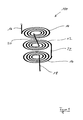
Fig. 1 zeigt eine Antennenanordnung 100 in schematischer Darstellung, die drei spiralförmige, metallische Antennenstrukturen 10, 12, 14 umfasst, die auf in Fig. 1 nicht dargestellten Leiterplatten aufgebracht sind. Durch die Leiterplatten gehen metallische Durchkontaktierungen 20 und 22, um die Antennenstrukturen miteinander elektrisch zu verbinden. Die drei Antennenstrukturen 10, 12, 14 haben gleichen Wickelsinn und sind in Serie geschaltet. Über Zuleitungen 16, 18 wird die so gebildete Antenne gespeist bzw. das Signal ausgelesen. Die Antennenstrukturen sind als Kupferleiterbahnen auf den Leiterplatten realisiert und haben eine Breite von nicht mehr als 150 µm. Ihre Höhe beträgt zwischen 35 und 75 µm.1 shows a schematic representation of an
Zum Beispiel an den Verbindungen zwischen den einzelnen Antennenstrukturen 10, 12, 14 können Vorrichtungen vorgesehen sein, mit denen einzelne Antennenstrukturen überbrückt bzw. zugeschaltet werden können. Auf diese Weise lassen sich Antennen mit unterschiedlichen Induktivitäten realisieren, je nachdem wie viele der Antennenstrukturen an der Antennenfunktion teilnehmen.For example, at the connections between the
Fig. 2 zeigt den seitlichen Querschnitt durch eine erfindungsgemäße Antennenanordnung mit vier Antennenstrukturen 10, 12, 14, 34. Auch diese Antennenstrukturen haben eine Breite von nicht mehr als 150 µm und eine Höhe zwischen 35 und 75 µm. Die relativen Maße, insbesondere die Dicken der die Antennestrukturen bildenden Leiterbahnen 10, 12, 14, 34 und der die Trägerplatten bildenden Leiterplatten 24, 26, 28, 30, 32 sind in Fig. 2 nicht maßstabsgetreu dargestellt.2 shows the lateral cross section through an antenna arrangement according to the invention with four
Die Antennenstrukturen mit den Bezugsziffern 14 und 34 befinden sich auf gegenüberliegenden Oberflächen der Leiterplatte 30. Die Antennenstruktur mit der Bezugsziffer 12 befindet sich auf einer der Leiterplatte mit der Bezugsziffer 30 abgewandten Oberfläche der Leiterplatte mit der Bezugsziffer 28. Schließlich befindet sich die Antennenstruktur mit der Bezugsziffer 10 auf derjenigen Oberfläche der Leiterplatte mit der Bezugsziffer 26, die der Leiterplatte mit der Bezugsziffer 28 abgewandt ist. Die Leiterplatten mit den Bezugsziffern 24 und 32, die den jeweiligen äußeren Abschluss bilden, tragen keine Antennenstruktur.The antenna structures with the
Deutlich ist in Fig. 2 zu erkennen, dass die Antennenstrukturen benachbarter Lagen gegeneinander versetzt sind. Auf diese Weise ist die kapazitive Kopplung zwischen den Antennenstrukturen benachbarter Lagen gering, obwohl auch die Dicke der Leiterplatten gering gehalten werden kann.It can clearly be seen in FIG. 2 that the antenna structures of adjacent layers are offset from each other. In this way, the capacitive coupling between the antenna structures of adjacent layers is low, although the thickness of the printed circuit boards can be kept low.
Die äußeren Leiterplatten 24, 32 dienen zum Schutz der empfindlichen dünnen Antennenstrukturen und können außerdem zum Tragen von zusätzlichen Schaltelementen zum Beispiel zur Anpassung dienen.The
Besonders einfach aufzubringen und handzuhaben sind Antennenstrukturen, die eckig ausgebildet sind, wie es die Draufsicht auf eine Antennenstruktur in Fig. 3 zeigt. Dabei ist es besonders vorteilhaft, wenn die innere Dimension Ri bei der gezeigten Anordnung etwa zweimal der äußeren Dimension Ra dividiert durch 5 entspricht.Particularly simple to apply and handle are antenna structures that are formed angular, as shown in the plan view of an antenna structure in Fig. 3. It is particularly advantageous if the inner dimension R i in the arrangement shown approximately twice the outer dimension R a divided by 5 corresponds.
Bei den gezeigten Ausführungsformen handelt es sich um Antennenanordnungen mit drei bzw. vier Lagen. Es sind auch Antennenanordnungen mit mehr oder weniger Lagen realisierbar, je nachdem welche Induktivitäten gewünscht sind.The embodiments shown are antenna arrangements with three or four layers. It is also possible antenna arrangements with more or fewer layers, depending on which inductances are desired.
In den Figuren nicht dargestellt ist ein zusätzlicher regelbarer Widerstand, der mit der Antennenanordnung verbunden ist, um produktionsabhängige Widerstandstoleranzen zu kompensieren, die gerade bei derartig kleinen Leiterbahnen störend auftreten können. Er kann zum Beispiel auf einer der äußeren Leiterplatten aufgebracht sein.Not shown in the figures is an additional controllable resistor which is connected to the antenna arrangement in order to compensate for production-dependent resistance tolerances, which may be troublesome especially with such small printed conductors. For example, it can be applied to one of the outer circuit boards.
Mit der erfindungsgemäßen Antennenanordnung können zum Beispiel Daten oder Steuersignale ausgetauscht werden. Außerdem eignet sich die Antennenanordnung zum drahtlosen Einspeisen von Energie zum Betrieb von Bauelementen, die mit der Antenne verbunden sind.With the antenna arrangement according to the invention, for example, data or control signals can be exchanged. In addition, the antenna arrangement is suitable for wirelessly feeding energy to the operation of devices that are connected to the antenna.
Insbesondere eignet sich die erfindungsgemäße Antennenanordnung als Ersatz für eine Luftspule, die in Verbindung mit zwei weiteren Spulen, zum Beispiel Ferritspulen, ein dreidimensional empfangendes bzw. sendendes Antennensystem zur Verfügung stellt.In particular, the antenna arrangement according to the invention is suitable as a replacement for an air coil which, in conjunction with two further coils, for example ferrite coils, provides a three-dimensionally receiving or transmitting antenna system.
- 10, 12, 1410, 12, 14
- Antennenstrukturen, LeiterbahnenAntenna structures, conductor tracks
- 16, 1816, 18
- Zuleitungenleads
- 20, 2220, 22
- Durchkontaktierungenvias
- 2424
- äußere Trägerschicht, Leiterplatteouter carrier layer, printed circuit board
- 26, 28, 3026, 28, 30
- Trägerschichten, LeiterplattenCarrier layers, printed circuit boards
- 3232
- äußere Trägerschicht, Leiterplatteouter carrier layer, printed circuit board
- 34, 3634, 36
- Antennenstrukturen, LeiterbahnenAntenna structures, conductor tracks
- 100100
- Antenneantenna
Claims (16)
Priority Applications (1)
| Application Number | Priority Date | Filing Date | Title |
|---|---|---|---|
| EP06002256A EP1816591A1 (en) | 2006-02-03 | 2006-02-03 | Antenna arrangement |
Applications Claiming Priority (1)
| Application Number | Priority Date | Filing Date | Title |
|---|---|---|---|
| EP06002256A EP1816591A1 (en) | 2006-02-03 | 2006-02-03 | Antenna arrangement |
Publications (1)
| Publication Number | Publication Date |
|---|---|
| EP1816591A1 true EP1816591A1 (en) | 2007-08-08 |
Family
ID=36649822
Family Applications (1)
| Application Number | Title | Priority Date | Filing Date |
|---|---|---|---|
| EP06002256A Withdrawn EP1816591A1 (en) | 2006-02-03 | 2006-02-03 | Antenna arrangement |
Country Status (1)
| Country | Link |
|---|---|
| EP (1) | EP1816591A1 (en) |
Citations (10)
| Publication number | Priority date | Publication date | Assignee | Title |
|---|---|---|---|---|
| DE1818161U (en) * | 1959-01-19 | 1960-09-15 | Siemens Ag | SPOOL COMPOSED OF INSULATION SHEETS PRINTED WITH SPIRAL SPOOL WRAPS. |
| DD290738A5 (en) | 1989-12-22 | 1991-06-06 | Veb Robotron-Messelektronik,"Otto Schoen",De | TRANSMIT AND / OR RECEIVER COIL FROM MULTIVILLATE PLATE |
| EP0547563B1 (en) | 1991-12-16 | 1996-03-06 | Siemens Aktiengesellschaft | Printed circuit board antenna |
| EP0769759A2 (en) * | 1995-10-19 | 1997-04-23 | Junghans Uhren Gmbh | Contactless chip card |
| EP0945381A2 (en) * | 1998-03-24 | 1999-09-29 | Elektro-Mechanik Gmbh | Apparatus for inductively measuring the position of a metal sheet |
| US6049461A (en) * | 1995-07-26 | 2000-04-11 | Giesecke & Devrient Gmbh | Circuit unit and a method for producing a circuit unit |
| JP2000306054A (en) * | 1999-04-23 | 2000-11-02 | Matsushita Electric Works Ltd | Scanner for non-contact identification data communication |
| EP1069645A2 (en) * | 1999-07-13 | 2001-01-17 | Shinko Electric Industries Co. Ltd. | Semiconductor device with an antenna and fabrication method therefor |
| FR2801728A1 (en) * | 1999-11-26 | 2001-06-01 | Valeo Securite Habitacle | Magnetic field emitting antenna for motor vehicle has spiral tracks printed on flat dielectric support |
| DE202004002448U1 (en) | 2004-02-16 | 2005-04-07 | Siemens Ag | Multilayer circuit board antenna for use in an identification system having a transponder and reader |
-
2006
- 2006-02-03 EP EP06002256A patent/EP1816591A1/en not_active Withdrawn
Patent Citations (10)
| Publication number | Priority date | Publication date | Assignee | Title |
|---|---|---|---|---|
| DE1818161U (en) * | 1959-01-19 | 1960-09-15 | Siemens Ag | SPOOL COMPOSED OF INSULATION SHEETS PRINTED WITH SPIRAL SPOOL WRAPS. |
| DD290738A5 (en) | 1989-12-22 | 1991-06-06 | Veb Robotron-Messelektronik,"Otto Schoen",De | TRANSMIT AND / OR RECEIVER COIL FROM MULTIVILLATE PLATE |
| EP0547563B1 (en) | 1991-12-16 | 1996-03-06 | Siemens Aktiengesellschaft | Printed circuit board antenna |
| US6049461A (en) * | 1995-07-26 | 2000-04-11 | Giesecke & Devrient Gmbh | Circuit unit and a method for producing a circuit unit |
| EP0769759A2 (en) * | 1995-10-19 | 1997-04-23 | Junghans Uhren Gmbh | Contactless chip card |
| EP0945381A2 (en) * | 1998-03-24 | 1999-09-29 | Elektro-Mechanik Gmbh | Apparatus for inductively measuring the position of a metal sheet |
| JP2000306054A (en) * | 1999-04-23 | 2000-11-02 | Matsushita Electric Works Ltd | Scanner for non-contact identification data communication |
| EP1069645A2 (en) * | 1999-07-13 | 2001-01-17 | Shinko Electric Industries Co. Ltd. | Semiconductor device with an antenna and fabrication method therefor |
| FR2801728A1 (en) * | 1999-11-26 | 2001-06-01 | Valeo Securite Habitacle | Magnetic field emitting antenna for motor vehicle has spiral tracks printed on flat dielectric support |
| DE202004002448U1 (en) | 2004-02-16 | 2005-04-07 | Siemens Ag | Multilayer circuit board antenna for use in an identification system having a transponder and reader |
Similar Documents
| Publication | Publication Date | Title |
|---|---|---|
| EP0756244B1 (en) | Electronic unit and method of producing that unit | |
| EP0092555B1 (en) | Tag-shaped identification device attachable to an object | |
| EP0547563B1 (en) | Printed circuit board antenna | |
| EP2036001B1 (en) | Transponder comprising an electronic memory chip and magnetic circular antenna | |
| DE60123004T2 (en) | CONTACTLESS DATA CARRIER | |
| EP2820768B1 (en) | Contactless data-transmitting device, security and/or value document containing said data-transmitting device, and method for producing the contactless data-transmitting device | |
| DE3221500A1 (en) | IDENTIFICATION ARRANGEMENT IN THE FORM OF AN OBJECT TO BE ATTACHED TO AN OBJECT, AND METHOD FOR THE PRODUCTION THEREOF | |
| WO2001009975A2 (en) | Radar sensor and radar antenna for monitoring the environment of a motor vehicle | |
| DE102010034156A1 (en) | film element | |
| EP2617100A1 (en) | Planar array antenna comprising antenna elements arranged in a plurality of planes | |
| DE202012007631U1 (en) | Electronic locking device | |
| EP1816591A1 (en) | Antenna arrangement | |
| EP1983467B1 (en) | Data carrier/transmission device and method for manufacturing it | |
| DE10019410B4 (en) | Flexible flat conductor | |
| EP2248242B1 (en) | Arrangement for the supply of at least one device located in a control panel or installation housing with auxiliary power | |
| EP1843281A1 (en) | Data carrier/transmission device and method for manufacturing such a data carrier/transmission device | |
| EP1695454A1 (en) | Electronic device provided with a security module | |
| EP1476622A1 (en) | Induction coil, in particular for a vehicle door locking system | |
| DE19842705C2 (en) | Antenna, in particular for an anti-theft protection system of a motor vehicle | |
| DE102022123949B3 (en) | Antenna structure, method of forming an antenna structure, annular device and method of forming an annular device | |
| EP3767748B1 (en) | Identification means for locking system | |
| DE202012012880U1 (en) | coil system | |
| DE102006044016A1 (en) | Stackable functional layer for a modular microelectronic system | |
| DE102009040537B4 (en) | Multilayer film element and method for providing a resonant circuit | |
| DE102004037682A1 (en) | A transmitting antenna arrangement for emitting a long-wave wake-up signal for an ID transmitter of a keyless vehicle access system |
Legal Events
| Date | Code | Title | Description |
|---|---|---|---|
| PUAI | Public reference made under article 153(3) epc to a published international application that has entered the european phase |
Free format text: ORIGINAL CODE: 0009012 |
|
| 17P | Request for examination filed |
Effective date: 20070119 |
|
| AK | Designated contracting states |
Kind code of ref document: A1 Designated state(s): AT BE BG CH CY CZ DE DK EE ES FI FR GB GR HU IE IS IT LI LT LU LV MC NL PL PT RO SE SI SK TR |
|
| AX | Request for extension of the european patent |
Extension state: AL BA HR MK YU |
|
| AKX | Designation fees paid |
Designated state(s): AT BE BG CH CY CZ DE DK EE ES FI FR GB GR HU IE IS IT LI LT LU LV MC NL PL PT RO SE SI SK TR |
|
| RAP1 | Party data changed (applicant data changed or rights of an application transferred) |
Owner name: DELPHI INTERNATIONAL OPERATIONS LUXEMBOURG S.A R.L |
|
| 17Q | First examination report despatched |
Effective date: 20170130 |
|
| STAA | Information on the status of an ep patent application or granted ep patent |
Free format text: STATUS: THE APPLICATION HAS BEEN WITHDRAWN |
|
| 18W | Application withdrawn |
Effective date: 20170224 |