EP1845581A2 - Multilayer planar balun transformer, mixers and amplifiers - Google Patents
Multilayer planar balun transformer, mixers and amplifiers Download PDFInfo
- Publication number
- EP1845581A2 EP1845581A2 EP07015125A EP07015125A EP1845581A2 EP 1845581 A2 EP1845581 A2 EP 1845581A2 EP 07015125 A EP07015125 A EP 07015125A EP 07015125 A EP07015125 A EP 07015125A EP 1845581 A2 EP1845581 A2 EP 1845581A2
- Authority
- EP
- European Patent Office
- Prior art keywords
- transformer
- port
- printed circuit
- circuit board
- accordance
- Prior art date
- Legal status (The legal status is an assumption and is not a legal conclusion. Google has not performed a legal analysis and makes no representation as to the accuracy of the status listed.)
- Granted
Links
- 230000005540 biological transmission Effects 0.000 abstract description 26
- 239000010410 layer Substances 0.000 description 31
- 238000010586 diagram Methods 0.000 description 11
- 239000000758 substrate Substances 0.000 description 11
- 239000002344 surface layer Substances 0.000 description 4
- 230000009466 transformation Effects 0.000 description 4
- 239000003989 dielectric material Substances 0.000 description 3
- 238000000034 method Methods 0.000 description 3
- 229910000679 solder Inorganic materials 0.000 description 3
- 239000004020 conductor Substances 0.000 description 2
- 230000008878 coupling Effects 0.000 description 2
- 238000010168 coupling process Methods 0.000 description 2
- 238000005859 coupling reaction Methods 0.000 description 2
- 238000005516 engineering process Methods 0.000 description 2
- 239000000463 material Substances 0.000 description 2
- 229910000859 α-Fe Inorganic materials 0.000 description 2
- RYGMFSIKBFXOCR-UHFFFAOYSA-N Copper Chemical compound [Cu] RYGMFSIKBFXOCR-UHFFFAOYSA-N 0.000 description 1
- 239000011324 bead Substances 0.000 description 1
- 230000015556 catabolic process Effects 0.000 description 1
- 238000006243 chemical reaction Methods 0.000 description 1
- 229910052802 copper Inorganic materials 0.000 description 1
- 239000010949 copper Substances 0.000 description 1
- 238000006731 degradation reaction Methods 0.000 description 1
- 230000001939 inductive effect Effects 0.000 description 1
- 239000002184 metal Substances 0.000 description 1
- 229910052751 metal Inorganic materials 0.000 description 1
- 238000012986 modification Methods 0.000 description 1
- 230000004048 modification Effects 0.000 description 1
- 239000002356 single layer Substances 0.000 description 1
- 238000004513 sizing Methods 0.000 description 1
- 238000005476 soldering Methods 0.000 description 1
Images


Classifications
-
- H—ELECTRICITY
- H01—ELECTRIC ELEMENTS
- H01F—MAGNETS; INDUCTANCES; TRANSFORMERS; SELECTION OF MATERIALS FOR THEIR MAGNETIC PROPERTIES
- H01F17/00—Fixed inductances of the signal type
- H01F17/0006—Printed inductances
- H01F17/0013—Printed inductances with stacked layers
-
- H—ELECTRICITY
- H01—ELECTRIC ELEMENTS
- H01P—WAVEGUIDES; RESONATORS, LINES, OR OTHER DEVICES OF THE WAVEGUIDE TYPE
- H01P5/00—Coupling devices of the waveguide type
- H01P5/08—Coupling devices of the waveguide type for linking dissimilar lines or devices
- H01P5/10—Coupling devices of the waveguide type for linking dissimilar lines or devices for coupling balanced with unbalanced lines or devices
-
- H—ELECTRICITY
- H01—ELECTRIC ELEMENTS
- H01F—MAGNETS; INDUCTANCES; TRANSFORMERS; SELECTION OF MATERIALS FOR THEIR MAGNETIC PROPERTIES
- H01F17/00—Fixed inductances of the signal type
- H01F17/0006—Printed inductances
- H01F17/0013—Printed inductances with stacked layers
- H01F2017/002—Details of via holes for interconnecting the layers
-
- H—ELECTRICITY
- H01—ELECTRIC ELEMENTS
- H01F—MAGNETS; INDUCTANCES; TRANSFORMERS; SELECTION OF MATERIALS FOR THEIR MAGNETIC PROPERTIES
- H01F21/00—Variable inductances or transformers of the signal type
- H01F21/12—Variable inductances or transformers of the signal type discontinuously variable, e.g. tapped
- H01F2021/125—Printed variable inductor with taps, e.g. for VCO
-
- H—ELECTRICITY
- H05—ELECTRIC TECHNIQUES NOT OTHERWISE PROVIDED FOR
- H05K—PRINTED CIRCUITS; CASINGS OR CONSTRUCTIONAL DETAILS OF ELECTRIC APPARATUS; MANUFACTURE OF ASSEMBLAGES OF ELECTRICAL COMPONENTS
- H05K1/00—Printed circuits
- H05K1/02—Details
- H05K1/14—Structural association of two or more printed circuits
- H05K1/141—One or more single auxiliary printed circuits mounted on a main printed circuit, e.g. modules, adapters
-
- H—ELECTRICITY
- H05—ELECTRIC TECHNIQUES NOT OTHERWISE PROVIDED FOR
- H05K—PRINTED CIRCUITS; CASINGS OR CONSTRUCTIONAL DETAILS OF ELECTRIC APPARATUS; MANUFACTURE OF ASSEMBLAGES OF ELECTRICAL COMPONENTS
- H05K1/00—Printed circuits
- H05K1/16—Printed circuits incorporating printed electric components, e.g. printed resistor, capacitor, inductor
- H05K1/165—Printed circuits incorporating printed electric components, e.g. printed resistor, capacitor, inductor incorporating printed inductors
-
- H—ELECTRICITY
- H05—ELECTRIC TECHNIQUES NOT OTHERWISE PROVIDED FOR
- H05K—PRINTED CIRCUITS; CASINGS OR CONSTRUCTIONAL DETAILS OF ELECTRIC APPARATUS; MANUFACTURE OF ASSEMBLAGES OF ELECTRICAL COMPONENTS
- H05K1/00—Printed circuits
- H05K1/18—Printed circuits structurally associated with non-printed electric components
- H05K1/182—Printed circuits structurally associated with non-printed electric components associated with components mounted in the printed circuit board, e.g. insert mounted components [IMC]
- H05K1/183—Components mounted in and supported by recessed areas of the printed circuit board
Definitions
- This invention generally relates to balun transformers that may be implemented on a printed circuit board or in surface mount packages, and more particularly to a transformer layout suitably adaptable for use in microwave modules where the transformer is integrated in the printed circuit board.
- a balun is a device designed to convert between balanced and unbalanced electrical signals, such as between, for example, a coaxial cable and a ladder line.
- Baluns may be considered as simple forms of transmission line transformers. The seminal work on transmission line transformers was done by Gustav Guanella in 1944. Guanella's transformer is described in U.S. Patent 2,470,307 . Guanella proposed coiling transmission lines to form a choke that would suppress the undesired mode in balanced-to-unbalanced matching applications. Guanella's transformer comprised a basic building block or a 1:1 balun. As is generally known, the choking reactance of Guanella's transformer isolates the input from the output.
- That reactance is usually obtained by coiling the transmission line around a ferrite core or by threading the line through ferrite beads.
- the objectives are to have the characteristic impedance, Z 0 , of the transmission line equal to the value of the load R L , which is generally referred to as the optimum characteristic impedance, and to have the choking reactance much greater than R L (and hence Z 0 ).
- Baluns may be implemented in a variety of ways using different types of transmission line elements.
- coaxial transmission line segments can be used to form baluns at relatively low frequencies.
- baluns are, however, difficult to integrate with other elements of microwave circuits where surface mount design techniques are used.
- baluns may be formed on printed circuit boards.
- Such baluns may be fabricated from stripline or other conductor materials that is formed on a substrate of a printed circuit board in a known manner.
- microstripline or other technologies have been used to form the conductive traces.
- surface mount designs require that components or devices are mounted on a printed circuit board having printed circuit traces on at least one surface of the board. The surface mount components connect to the terminals of the traces using known soldering techniques.
- FIG. 1B there is shown a schematic circuit diagram of a prior art transformer. Due to the asymmetry cased by grounding at port 5, it is typically necessary for this balun transformer to function at the junction point where L1 is tapped. This point does not always have a zero potential for the differential signal. This usually leads to degradation in performance.
- the transformer of FIG. 1B is commonly used in diode double-balanced mixers normally followed by a Guanella balun transformer.
- U.S. patent 6,294,965 to Merrill et al. modifies the transformer of FIG. 1B but the summing function needed for mixers and to establish a DC supply point is not provided.
- FIG. 1C shows a equivalent schematic circuit diagram of the transformer described in the '965 patent.
- the present invention provides a balun transformer that may be implemented on a printed circuit board so as to advantageously allow more flexibility in the layout of the circuit elements.
- An aspect of the present invention is a surface mountable balun transformer that is preferably integratable into a printed circuit board.
- the transformer preferably comprises a first C-shaped line segment having a first end and a second end disposed on the layer of the printed circuit board and a second C-shaped line segment having a first end and a second end disposed on a layer of the printed circuit board.
- the first ends of each of the C-shaped line segments preferably provide a balanced port for connecting to the transformer and the second end of the first C-shaped line segments preferably provides an unbalanced port for connecting to the transformer.
- the surface mountable balun transformer may further comprise a third C-shaped line segment broadside vertically coupled to the first C-shaped line segment.
- the surface mountable balun transformer may further desirably comprise a fourth C-shaped line segment broadside vertically coupled to the second C-shaped line segment.
- the third and fourth C-shaped line segments are preferably separated form the first and second C-shaped line segments by a dielectric material.
- this aspect of the present invention may further comprise third and fourth C-shaped line segments broadside vertically partially respectively coupled to the first and second C-shaped line segments.
- the balanced port of the surface mountable balun transformer is desirably disposed opposite the unbalanced port on the layer of the printed circuit board.
- this aspect of the present invention may further desirably comprise a first port formed by a metallized via hole that couples the balun transformer to the power plane of the printed circuit.
- each of the C-shaped line segments may be desirably folded to form a pair of U-shaped sections that are connected in series.
- the balun transformer may further comprise a first port formed by a metallized via that extends between the layers of the printed circuit board and wherein the first port is located adjacent the balanced port and connected to the second end of the second line segment and is shorted to a ground through the metallized via.
- the present invention may comprise a printed circuit board.
- the printed circuit board preferably comprises a first planar layer and a second planar layer disposed opposite and parallel to the first planar layer; a first C-shaped line segment having a first end and a second end disposed on the first planar layer of the printed circuit board; and a second C-shaped line segment broadside vertically coupled to the first C-shaped line segment, the second C-shaped line segment having a first end and a second end disposed on a second planar layer of the printed circuit board.
- the printed circuit board also preferably includes a third C-shaped line segment having a first end and a second end disposed on the first planar layer of the printed circuit board; a fourth C-shaped line segment broadside vertically coupled to the third C-shaped line segment, the fourth C-shaped line segment having a first end and a second end disposed on the second planar layer of the printed circuit board; and a fifth line segment having an end connecting the second ends of the first and third line segments and another end forming an unbalanced port.
- the first ends of the first and third line segments preferably form a balanced port and the first end of the second line segment preferably forms an unbalanced port.
- each of the C-shaped line segments are preferably folded to form a pair of U-shaped sections that are connected in series.
- the second end of the second line segment is desirably connected to ground on the second layer of the board through a metallized via.
- the present invention comprises a printed circuit board that preferably comprises a first planar layer and a second planar disposed opposite and parallel to the first planar layer; an electronic circuit disposed within a cavity formed within the first planar layer; a first balun transformer having a pair of C-shaped broadside vertically coupled lines connected in series so as to form a first unbalanced port on the first planar layer and a first balanced port on the first planar opposite the unbalanced port; and a second balun transformer having a pair of C-shaped broadside vertically coupled lines connected in series so as to form a second unbalanced port on the first planar layer and a second balanced port on the first planar layer opposite the second unbalanced port.
- first and second unbalanced ports are desirably connected to the electronic circuit.
- the electronic circuit may desirably comprise a diode ring, mixer or a power amplifier.
- FIG. 1A is a schematic circuit diagram of a prior art Guanella 1:4 impedance transformer.
- FIG. 1B depicts a schematic of a prior art transformer used in a double balanced mixer.
- FIG. 1C illustratively depicts a schematic of a prior art balun transformer.
- FIG. 2 illustratively depicts an equivalent schematic circuit diagram of a balun transformer in accordance with an aspect of the present invention.
- FIG. 3 illustratively depicts a perspective side view of a layout of a balun transformer in accordance with an aspect of the present invention.
- FIG. 4 illustratively depicts a perspective side view of a layout of a balun transformer in accordance with an aspect of the present invention.
- FIG. 5 illustratively depicts a side view of a layout of a balun transformer in accordance with an aspect of the present invention.
- FIG. 6 illustratively depicts a schematic of a transformer in accordance with an aspect of the present invention.
- FIG. 7 illustratively depicts an equivalent schematic of FIG. 6 in accordance with an aspect of the present invention.
- FIG. 8 illustratively depicts a perspective side view of a layout of a balun transformer in accordance with an aspect of the present invention.
- FIG. 9 illustratively depicts a circuit diagram of a double balanced diode mixer in accordance with an aspect of the present invention.
- FIG. 10 illustratively depicts a perspective view of a double balanced diode mixer layout in accordance with an aspect of the present invention.
- FIG. 11 illustratively depicts a schematic circuit diagram of a double balanced mixer in accordance with an aspect of the present invention.
- FIG. 12 illustratively depicts a perspective view of a double balanced mixer layout in accordance with an aspect of the present invention.
- FIG. 13 illustratively depicts a schematic circuit diagram of a push-pull amplifier in accordance with an aspect of the present invention.
- FIG. 14 illustratively depicts a reflective mixer in accordance with an aspect of the present invention.
- FIG. 15 illustratively depicts double balanced FET mixer in accordance with an aspect of the present invention.
- FIG. 16 illustratively depicts a perspective view of a layout of a multi-layer planar circuit board in accordance with an aspect of the present invention.
- FIG. 2 there is shown an equivalent schematic circuit diagram of a balun transformer 200 in accordance with an aspect of the present invention.
- the transformer 200 includes five ports labeled ports 1, 2, 3, 4 and 5.
- Z load 4 ⁇ Zo 2 Z source
- Zo Z o odd * ⁇ Z o even
- Z o is a characteristic impedance
- Z o odd and Z o even are the odd and even mode impedances of the lines, respectively.
- the structure when port 2 is grounded, the structure desirably operates as an impedance-transforming balun with port 1 as a single-ended or unbalanced port and ports 3 and 5 as a differential or balanced port.
- ports 2 and 4 when operating as a balun transformer ports 2 and 4 are preferably grounded.
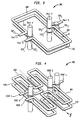
- FIG. 3 there is shown a layout of a surface mountable balun transformer 300 in accordance with an aspect of the present invention.
- the transformer 300 is advantageously adapted for use in microwave modules circuits where the transformers are integrated in the printed circuit board and the active devices or components are mounted in a cavity.
- the transformer 300 includes four lines segments 304, 308, 312 and 316. Each of the line segments forms a trace on a printed circuit board. Each trace may comprise a stripline or microstripline. Striplines or microstriplines are transmission lines which can be formed as a conductive metal trace based in a dielectric media with two parallel ground planes on both sides balun dielectric surface. For clarity, the dielectric media or substrate is not shown in FIG.
- the dielectric substrate frequently includes two parallel ground planes on both surfaces of the substrate.
- the layer of conductive material comprises copper and the dielectric substrate preferably comprises a low loss high frequency laminate or an equivalent thereof.
- the impedance of the line segments is determined by the dimension of the segments, and the type of dielectric material that is used. As is known to those skilled in the art, the selection of the dielectric material and the sizing of the line segments may be chosen to meet the particular design requirements and/or constraints.
- a coupled line segment is generally known as a structure that comprises two lines having a constant distance between them.
- the coupled line segments may be made as two parallel traces on the same layer with ground planes on the layers above and below the layer with the traces, or as parallel traces placed on two adjacent layers.
- the printed circuit board may include other surface mounted components which can be electrically connected to the ports of the balun transformer 300.
- the first line segment 304 includes a first end 304 1 , which forms port 3.
- the first line segment 304 also includes a second end 304 2 , which is connected to port 2.
- port 2 is depicted as a separate cylindrical block, it is preferably formed as a via. This is also the case for port 4 and any other similarly depicted element herein.
- the line segment 308 includes a first end 308 1 and a second end 308 2 . As shown, the first end 308 1 forms port 5 while the second end 308 2 forms port 1.
- Each of the line segments include a broadside that is defined by the lateral dimension D of the trace on the substrate.
- each of the line segments depicted in FIG. 3 may comprise the same lateral dimension D, the invention is not so limited. As is known in the art, the dimensions may be varied, particularly the traces that are located on opposed vertical surfaces, to meet the design requirements.
- each of the ports 2 and 4 are preferably formed by a via or via-hole.
- each of these ports are connected by the via to the power planes of the printed circuit board on which the line segments are traced.
- both of these ports are shorted to ground.
- the first and second ends of line segment 316 i.e., ends 316 1 and 316 2 , are connected to the vias forming ports 2 and 4.
- the first end 312, of the line segment 312 is connected to port 4.
- the second line segment 312 2 is also connected to a via.
- each of the line segments 304, 308, 312 and 316 comprise C-shaped line segments or conductive traces on a surface of the printed circuit board. In a multilayer structure, these line segments or conductive traces may also be located in the printed circuit board. As is also shown in FIG. 3, the line segments 304 and 312 comprise broadside coupled lines. In addition, the line segments 308 and 316 similarly comprise broadside coupled line segments or transmission lines. Further, the first ends of the line segments 308 1 and 304 1 comprise the differential or balanced port of the transformer 300. The second end 308 2 of the line segment 308 forms the unbalanced port of the transformer 300.
- both the balanced and unbalanced ports lie in the same plane or on the same surface of the printed circuit board onto which the transformer 300 is fabricated.
- having the differential or balanced output on a single layer makes it possible to directly interface active components mounted in a cavity on the printed circuit board.
- the layout requires only two signal layers.
- the transmission lines are partially coupled, higher-mode impedances can be achieve, thereby keeping the ohmic losses and the occupied area small.
- the transformer 300 is desirable for use in applications comprising of a frequency range between 0.1 to 20 GHz.
- a trace width of approximately 0.08 inches (8 mils) can be used to implement the circuitry and layouts described herein, the width of the trace depends on the thickness of the substrate material.
- FIG. 4 there is shown a surface mountable balun transformer 400 in accordance with an additional aspect of the present invention.
- the transformer 400 operates similarly to the transformer 300 of FIG. 3.
- the line segments that comprise the coupled transmission lines are shaped differently. They are folded.
- each of the line segments 404, 408, 412 and 416 are formed as pairs of U-shaped traces connected in series and symmetrical about the y-axis.
- the layout of FIG. 4 advantageously allows for better area utilization on the printed circuit board and allows for greater flexibility, which is generally desirable where compactness is of importance.
- ports 3 and 5 comprise the balanced ports for connecting or coupling a signal to the transformer 400.
- Port 1 comprises the unbalanced port connecting to the transformer.
- Ports 2 and 4 preferably comprise vias that are connected to the board's power planes and are preferably grounded.
- the board 500 includes a first surface layer 510, a middle layer 516 and a second surface layer 520.
- the first and second surface layers 510, 520 comprise planar surfaces that extend substantially parallel to one another.
- the middle layer 516 separating these two surface layers preferably comprises a dielectric.
- Each of the blocks C1, C2, C3 and C4 illustratively depict a line segment or trace on the surfaces shown. These traces may comprise C-shaped or the folded shape of FIG. 4 in accordance with the foregoing description.
- Line segments C1 and C2 comprise broadside vertically partially coupled transmission lines.
- Line segments C3 and C4 likewise comprise broadside vertically partially coupled transmission lines. As discussed above, by vertically partially coupling the transmission lines along their broadside, higher mode impedance may be achieved while keeping the ohmic losses low. Note, however, the coupled lines may also comprise broadside vertically fully coupled transmission lines by aligning C1 directly above C2 and C3 directly above C4.
- an aspect of the present invention is a printed line structure preferably comprising at least two C-shaped broadside coupled lines connected in series at one side so that ports 3 and 5 differentially exit the structure.
- port 4 is preferably formed by a via that can be connected directly to the board's power planes or can be used to tap a common mode signal. Further, the lines are connected in parallel so that port 1 exits on the opposite side of the structure and port 2 is formed by a via that can also be connected directly to the board's power planes.
- ports 5 and 3 are taken directly from the couplers
- port 4 is the junction point of both C-shaped couplers and ports 1 and 2 are taken through metallized via holes.
- the transmission lines may be folded as is shown in FIG. 4.
- the coupled lines are broadside vertically partially coupled transmission lines as shown in FIG. 5, higher odd-mode impedance may be achieve while keeping the ohmic losses low.
- the coupled lines may be broadside vertically fully coupled transmission lines.
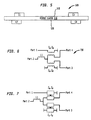
- FIG. 6 illustratively depicts a schematic circuit diagram of a transformer 700 in accordance with another aspect of the present invention.
- a differential signal between ports 3 and 4 is transformed to a single ended signal at port 1 with an impedance transformation Z 1 .
- a common mode signal on ports 3 and 4 is transformed as a single ended signal at port 2.
- the inductive element L1 is provided to improve the high frequency performance of the differential single ended (balun) transformation.
- L1 may comprise a portion of the transmission line.
- Port 2 may also be used for supplying a DC current to the circuit without the need for additional components.
- a printed circuit board layout in accordance with FIG. 6 desirably allows a transformer to provide a differential to the single ended conversion by grounding one of the ports.
- FIG. 7 is an equivalent schematic circuit diagram of the transformer of FIG. 6.
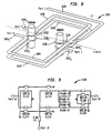
- FIG. 8 illustratively depicts a layout of a surface mountable balun transformer 1000 in accordance with an aspect of the present invention.
- the transformer 1000 includes four ports labeled as ports 1, 2, 3 and 4.
- the transformer 1000 includes five line segments 1004, 1008, 1012, 1016 and 1020.
- the line segments 1004, 1008 are disposed on a first layer of a substrate (not shown) of a printed circuit board.
- Each of these line segments 1004, 1008 includes first ends 1004 1 , 1008 1 , respectively.
- Each of these first ends comprises the balanced ports, port 3, port 4, of the transformer 1000.
- the line segments 1004, 1008 would form two C-shaped traces in a plane above the x-axis except that they are joined at what would comprise their other end. That other end which is located near via 1026 is illustratively depicted using arrow 1030.
- the fifth line segment 1020 extends from approximately location 1030 running parallel and adjacent to two sections of line segment 1008 as shown.
- the line segment 1020 comprises the inductor L1 shown in FIGS. 6 and 7.
- line segment 1012 include a first end 1012 1 and a second end 1012 2 .
- Line segment 1012 is disposed in a plane on a second surface that extends parallel to the first surface of the substrate.
- line segments 1004 and 1012 comprise broadside vertically coupled transmission lines.
- line segments 1008 and 1016 comprise broadside vertically coupled transmission lines.
- line segment 1016 includes a first end 1016 1 and a second end 1016 2 .
- the first end 1016 1 terminates on the grounding via 1026.
- the second 1016 2 terminates on the grounding via 1032 along with second end 1012 2 .
- We conveniently refer to the transformer 1000 as comprising a 0/180 four port network or a microwave hybrid layout.
- FIG. 9 illustratively depicts a schematic circuit diagram of a double balanced diode mixer 1100.
- the mixer 1100 may be implemented and laid out on a printed circuit board as shown in FIG. 10.
- the mixer layout 1200 of FIG. 10 includes a pair of balun transformers 1204, 1208 implemented in accordance with the foregoing aspects of the present invention.
- each of these transformers 1204, 1208 comprise pairs of C-shaped broadside vertically coupled transmission lines.
- a local oscillator signal is applied to the unbalanced LO port 1212.
- the local oscillator signal is then coupled by the transformer 1208 to the diode ring 1214 via the differential or balanced ports 1216 1 , 1216 2 .
- An intermediate frequency signal appearing on the IF port 1220 is also coupled to the diode ring 1214 at the balanced ports 1216 1 and 1216 2 .
- the balanced ports 1224 1 , 1224 2 of the other transformer 1204 couple the mixed signals to the unbalanced RF port 1230 of the transformer 1204.
- a mixer implemented in accordance with the circuitry 1200 may function to either mix up or mix down a signal. That is, it may comprise a circuit that mixes the local oscillator signal with the intermediate frequency signal to produce a higher frequency RF signal. On the other hand, it may comprise a signal that mixes the local oscillator signal with the RF signal to produce an intermediate frequency signal.
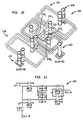
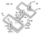
- FIG. 11 shows a double balanced mixer 1300 that is laid out in accordance with the surface mountable balun transformers shown in FIG. 12.
- the mixer 1400 of FIG. 12 includes two balun transformers 1410, 1420.
- Balun transformer 1410 comprises the layout shown and discussed above in relation to FIG. 3.
- Transformer 1420 comprises the hybrid layout discussed and shown in FIG. 8.
- the hybrid layout 1420 allows the intermediate frequency signal to be more conveniently coupled and mixed with the signal at the local oscillator port. In that regard, both the signals are coupled to the unbalanced port 1424. Those signals are then provided to the diode ring 1428 via the balanced ports 1430 1 and 1430 2 .
- the RF signal from the diode ring 1428 is coupled to the unbalanced port 1434 of the transformer 1410 via the balanced ports 1436 1 and 1436 2 .
- the hybrid transformer 1420 allows for a less complicated layout.
- the mixer may operate as a down converter.
- FIGS. 13, 14 and 15 illustratively depicts equivalent circuits of other electronic devices that may be implemented using the layouts shown and discussed above in accordance with further aspects of the present invention.
- FIG. 13 illustratively depicts an equivalent circuit of the push-pull amplifier.
- FIG. 14 illustratively depicts an equivalent circuit of a reflective FET mixer and
- FIG. 15 illustratively depicts the equivalent circuit of double balanced FET mixer in accordance with additional aspects of the present invention.
- Each of these devices or electronic circuits may be advantageously implemented using the transformer layouts described above. By using our transformers in these circuits, the frequency bandwidth is advantageously extended while maintaining low loss performance.
- circuits implemented using the transformers disclosed herein reduce (and in some cases prevent) resonance from occurring within the desired bandwidth and provides stable impedance. Furthermore, such circuits will also advantageously exhibit good phase/amplitude matching.
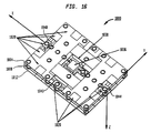
- FIG. 16 there shown a multilayer printed circuit board 1800 implemented in accordance with an aspect of the present invention.
- This board includes three layers 1804, 1808 and 1812. Each of these layers comprises a planar surface, each surface extending along the x and y axes as shown. Each of the surfaces also extends parallel to each other and are disposed relative to each other along the z axis.
- the board includes a number of solder pads 1820 and a cavity 1830.
- a diode ring 1836 is placed in the cavity 1830. The diode ring is then connected to the transformer baluns as discussed above with respect to FIGS. 10 or 14.
- the IF port may be formed at solder pad 1840.
- the RF and IF ports may be formed at solder pads 1844 and 1848, or vice versa.
Abstract
Description
- This application claims the benefit of the filing date of
United States Provisional Patent Application No. 60/710,570, filed August 23, 2005 - This invention generally relates to balun transformers that may be implemented on a printed circuit board or in surface mount packages, and more particularly to a transformer layout suitably adaptable for use in microwave modules where the transformer is integrated in the printed circuit board.
- A balun is a device designed to convert between balanced and unbalanced electrical signals, such as between, for example, a coaxial cable and a ladder line. Baluns may be considered as simple forms of transmission line transformers. The seminal work on transmission line transformers was done by Gustav Guanella in 1944. Guanella's transformer is described in
U.S. Patent 2,470,307 . Guanella proposed coiling transmission lines to form a choke that would suppress the undesired mode in balanced-to-unbalanced matching applications. Guanella's transformer comprised a basic building block or a 1:1 balun. As is generally known, the choking reactance of Guanella's transformer isolates the input from the output. That reactance is usually obtained by coiling the transmission line around a ferrite core or by threading the line through ferrite beads. In general, the objectives are to have the characteristic impedance, Z0, of the transmission line equal to the value of the load RL, which is generally referred to as the optimum characteristic impedance, and to have the choking reactance much greater than RL (and hence Z0). By combining coil transmission lines in parallel-series arrangements, Guanella was able to demonstrate very broad baluns, with ratios of 1:n2 where n is the number of transmission lines. FIG. 1A shows a schematic for Guanella's 1:4 balun. - Baluns may be implemented in a variety of ways using different types of transmission line elements. For example, coaxial transmission line segments can be used to form baluns at relatively low frequencies. These types of baluns are, however, difficult to integrate with other elements of microwave circuits where surface mount design techniques are used. Where such techniques are employed, baluns may be formed on printed circuit boards. Such baluns may be fabricated from stripline or other conductor materials that is formed on a substrate of a printed circuit board in a known manner. In addition to stripline, microstripline or other technologies have been used to form the conductive traces. In general, surface mount designs require that components or devices are mounted on a printed circuit board having printed circuit traces on at least one surface of the board. The surface mount components connect to the terminals of the traces using known soldering techniques.
- Turning now to FIG. 1B, there is shown a schematic circuit diagram of a prior art transformer. Due to the asymmetry cased by grounding at
port 5, it is typically necessary for this balun transformer to function at the junction point where L1 is tapped. This point does not always have a zero potential for the differential signal. This usually leads to degradation in performance. The transformer of FIG. 1B is commonly used in diode double-balanced mixers normally followed by a Guanella balun transformer.U.S. patent 6,294,965 to Merrill et al. modifies the transformer of FIG. 1B but the summing function needed for mixers and to establish a DC supply point is not provided. - FIG. 1C shows a equivalent schematic circuit diagram of the transformer described in the '965 patent.
- In surface mount applications it is desirable to have the various circuit elements and conductive traces desirably shaped to meet design demands. The present invention provides a balun transformer that may be implemented on a printed circuit board so as to advantageously allow more flexibility in the layout of the circuit elements.
- An aspect of the present invention is a surface mountable balun transformer that is preferably integratable into a printed circuit board. The transformer preferably comprises a first C-shaped line segment having a first end and a second end disposed on the layer of the printed circuit board and a second C-shaped line segment having a first end and a second end disposed on a layer of the printed circuit board. Further in accordance with this aspect of the present invention, the first ends of each of the C-shaped line segments preferably provide a balanced port for connecting to the transformer and the second end of the first C-shaped line segments preferably provides an unbalanced port for connecting to the transformer.
- Further in accordance with this aspect of the present invention, the surface mountable balun transformer may further comprise a third C-shaped line segment broadside vertically coupled to the first C-shaped line segment. In addition, the surface mountable balun transformer may further desirably comprise a fourth C-shaped line segment broadside vertically coupled to the second C-shaped line segment.
- Further in accordance with this aspect of the present invention, the third and fourth C-shaped line segments are preferably separated form the first and second C-shaped line segments by a dielectric material.
- Further still, this aspect of the present invention may further comprise third and fourth C-shaped line segments broadside vertically partially respectively coupled to the first and second C-shaped line segments.
- Further in accordance with this aspect of the present invention, the balanced port of the surface mountable balun transformer is desirably disposed opposite the unbalanced port on the layer of the printed circuit board.
- In addition, this aspect of the present invention may further desirably comprise a first port formed by a metallized via hole that couples the balun transformer to the power plane of the printed circuit.
- Further still in accordance with this aspect of the present invention, each of the C-shaped line segments may be desirably folded to form a pair of U-shaped sections that are connected in series.
- In addition, the balun transformer may further comprise a first port formed by a metallized via that extends between the layers of the printed circuit board and wherein the first port is located adjacent the balanced port and connected to the second end of the second line segment and is shorted to a ground through the metallized via.
- In another aspect, the present invention may comprise a printed circuit board. The printed circuit board preferably comprises a first planar layer and a second planar layer disposed opposite and parallel to the first planar layer; a first C-shaped line segment having a first end and a second end disposed on the first planar layer of the printed circuit board; and a second C-shaped line segment broadside vertically coupled to the first C-shaped line segment, the second C-shaped line segment having a first end and a second end disposed on a second planar layer of the printed circuit board. The printed circuit board also preferably includes a third C-shaped line segment having a first end and a second end disposed on the first planar layer of the printed circuit board; a fourth C-shaped line segment broadside vertically coupled to the third C-shaped line segment, the fourth C-shaped line segment having a first end and a second end disposed on the second planar layer of the printed circuit board; and a fifth line segment having an end connecting the second ends of the first and third line segments and another end forming an unbalanced port. Further in accordance with this aspect of the present invention, the first ends of the first and third line segments preferably form a balanced port and the first end of the second line segment preferably forms an unbalanced port.
- In accordance with this aspect of the present invention each of the C-shaped line segments are preferably folded to form a pair of U-shaped sections that are connected in series.
- In addition, the second end of the second line segment is desirably connected to ground on the second layer of the board through a metallized via.
- In another aspect, the present invention comprises a printed circuit board that preferably comprises a first planar layer and a second planar disposed opposite and parallel to the first planar layer; an electronic circuit disposed within a cavity formed within the first planar layer; a first balun transformer having a pair of C-shaped broadside vertically coupled lines connected in series so as to form a first unbalanced port on the first planar layer and a first balanced port on the first planar opposite the unbalanced port; and a second balun transformer having a pair of C-shaped broadside vertically coupled lines connected in series so as to form a second unbalanced port on the first planar layer and a second balanced port on the first planar layer opposite the second unbalanced port. In accordance with this aspect with the present invention, first and second unbalanced ports are desirably connected to the electronic circuit.
- In accordance with this aspect of the present invention, the electronic circuit may desirably comprise a diode ring, mixer or a power amplifier.
- FIG. 1A is a schematic circuit diagram of a prior art Guanella 1:4 impedance transformer.
- FIG. 1B depicts a schematic of a prior art transformer used in a double balanced mixer.
- FIG. 1C illustratively depicts a schematic of a prior art balun transformer.
- FIG. 2 illustratively depicts an equivalent schematic circuit diagram of a balun transformer in accordance with an aspect of the present invention.
- FIG. 3 illustratively depicts a perspective side view of a layout of a balun transformer in accordance with an aspect of the present invention.
- FIG. 4 illustratively depicts a perspective side view of a layout of a balun transformer in accordance with an aspect of the present invention.
- FIG. 5 illustratively depicts a side view of a layout of a balun transformer in accordance with an aspect of the present invention.
- FIG. 6 illustratively depicts a schematic of a transformer in accordance with an aspect of the present invention.
- FIG. 7 illustratively depicts an equivalent schematic of FIG. 6 in accordance with an aspect of the present invention.
- FIG. 8 illustratively depicts a perspective side view of a layout of a balun transformer in accordance with an aspect of the present invention.
- FIG. 9 illustratively depicts a circuit diagram of a double balanced diode mixer in accordance with an aspect of the present invention.
- FIG. 10 illustratively depicts a perspective view of a double balanced diode mixer layout in accordance with an aspect of the present invention.
- FIG. 11 illustratively depicts a schematic circuit diagram of a double balanced mixer in accordance with an aspect of the present invention.
- FIG. 12 illustratively depicts a perspective view of a double balanced mixer layout in accordance with an aspect of the present invention.
- FIG. 13 illustratively depicts a schematic circuit diagram of a push-pull amplifier in accordance with an aspect of the present invention.
- FIG. 14 illustratively depicts a reflective mixer in accordance with an aspect of the present invention.
- FIG. 15 illustratively depicts double balanced FET mixer in accordance with an aspect of the present invention.
- FIG. 16 illustratively depicts a perspective view of a layout of a multi-layer planar circuit board in accordance with an aspect of the present invention.
- Turning now to FIG. 2, there is shown an equivalent schematic circuit diagram of a
balun transformer 200 in accordance with an aspect of the present invention. Thetransformer 200 includes five ports labeledports 
where
odd and Zoeven are the odd and even mode impedances of the lines, respectively. In accordance with this aspect of the present invention, whenport 2 is grounded, the structure desirably operates as an impedance-transforming balun withport 1 as a single-ended or unbalanced port andports balun transformer ports - Turning now to FIG. 3, there is shown a layout of a surface
mountable balun transformer 300 in accordance with an aspect of the present invention. Thetransformer 300 is advantageously adapted for use in microwave modules circuits where the transformers are integrated in the printed circuit board and the active devices or components are mounted in a cavity. Thetransformer 300 includes fourlines segments line segments line segments - In addition, a coupled line segment is generally known as a structure that comprises two lines having a constant distance between them. In a multi-layer structure, such as depicted in FIG. 3, the coupled line segments may be made as two parallel traces on the same layer with ground planes on the layers above and below the layer with the traces, or as parallel traces placed on two adjacent layers. As is discussed in further detail below, the printed circuit board may include other surface mounted components which can be electrically connected to the ports of the
balun transformer 300. - As is shown in FIG. 3, the
first line segment 304 includes afirst end 3041, which formsport 3. Thefirst line segment 304 also includes asecond end 3042, which is connected toport 2. Note that althoughport 2 is depicted as a separate cylindrical block, it is preferably formed as a via. This is also the case forport 4 and any other similarly depicted element herein. Theline segment 308 includes afirst end 3081 and asecond end 3082. As shown, thefirst end 3081forms port 5 while thesecond end 3082forms port 1. - Each of the line segments include a broadside that is defined by the lateral dimension D of the trace on the substrate. Although in the preferred embodiment, each of the line segments depicted in FIG. 3 may comprise the same lateral dimension D, the invention is not so limited. As is known in the art, the dimensions may be varied, particularly the traces that are located on opposed vertical surfaces, to meet the design requirements.
- As mentioned above, each of the
ports line segment 316, i.e., ends 3161 and 3162, are connected to thevias forming ports first end 312, of theline segment 312 is connected toport 4. Thesecond line segment 3122 is also connected to a via. - In accordance with an aspect of the present invention, each of the
line segments line segments line segments line segments transformer 300. Thesecond end 3082 of theline segment 308 forms the unbalanced port of thetransformer 300. In accordance with an aspect of the present invention, both the balanced and unbalanced ports lie in the same plane or on the same surface of the printed circuit board onto which thetransformer 300 is fabricated. In this regard, having the differential or balanced output on a single layer makes it possible to directly interface active components mounted in a cavity on the printed circuit board. In addition, in accordance with this aspect of the present invention, the layout requires only two signal layers. Furthermore, if the transmission lines are partially coupled, higher-mode impedances can be achieve, thereby keeping the ohmic losses and the occupied area small. When built using standard printed circuit board technology, thetransformer 300 is desirable for use in applications comprising of a frequency range between 0.1 to 20 GHz. Although we found that a trace width of approximately 0.08 inches (8 mils) can be used to implement the circuitry and layouts described herein, the width of the trace depends on the thickness of the substrate material. - Turning now to FIG. 4, there is shown a surface
mountable balun transformer 400 in accordance with an additional aspect of the present invention. Functionally, thetransformer 400 operates similarly to thetransformer 300 of FIG. 3. However, the line segments that comprise the coupled transmission lines are shaped differently. They are folded. In particular, each of theline segments ports transformer 400.Port 1 comprises the unbalanced port connecting to the transformer.Ports - Turning now to FIG. 5, there is shown a side view of a printed
circuit board 500 in accordance with a further aspect of the present invention. As shown in FIG. 5, theboard 500 includes afirst surface layer 510, amiddle layer 516 and asecond surface layer 520. The first and second surface layers 510, 520 comprise planar surfaces that extend substantially parallel to one another. Themiddle layer 516 separating these two surface layers preferably comprises a dielectric. Each of the blocks C1, C2, C3 and C4 illustratively depict a line segment or trace on the surfaces shown. These traces may comprise C-shaped or the folded shape of FIG. 4 in accordance with the foregoing description. Line segments C1 and C2 comprise broadside vertically partially coupled transmission lines. Line segments C3 and C4 likewise comprise broadside vertically partially coupled transmission lines. As discussed above, by vertically partially coupling the transmission lines along their broadside, higher mode impedance may be achieved while keeping the ohmic losses low. Note, however, the coupled lines may also comprise broadside vertically fully coupled transmission lines by aligning C1 directly above C2 and C3 directly above C4. - In accordance with the foregoing description, an aspect of the present invention is a printed line structure preferably comprising at least two C-shaped broadside coupled lines connected in series at one side so that
ports port 4 is preferably formed by a via that can be connected directly to the board's power planes or can be used to tap a common mode signal. Further, the lines are connected in parallel so thatport 1 exits on the opposite side of the structure andport 2 is formed by a via that can also be connected directly to the board's power planes. In accordance with this aspect of the present invention,ports port 4 is the junction point of both C-shaped couplers andports - FIG. 6 illustratively depicts a schematic circuit diagram of a
transformer 700 in accordance with another aspect of the present invention. In accordance with FIG. 6, a differential signal betweenports port 1 with an impedance transformation Z1. Z1 is given by the following equation:
ports port 2. The inductive element L1 is provided to improve the high frequency performance of the differential single ended (balun) transformation. L1 may comprise a portion of the transmission line.Port 2 may also be used for supplying a DC current to the circuit without the need for additional components. In accordance with a further aspect of the present invention, a printed circuit board layout in accordance with FIG. 6 desirably allows a transformer to provide a differential to the single ended conversion by grounding one of the ports. FIG. 7 is an equivalent schematic circuit diagram of the transformer of FIG. 6. - FIG. 8 illustratively depicts a layout of a surface
mountable balun transformer 1000 in accordance with an aspect of the present invention. Thetransformer 1000 includes four ports labeled asports transformer 1000 includes fiveline segments line segments line segments port 3,port 4, of thetransformer 1000. Theline segments arrow 1030. - The
fifth line segment 1020 extends from approximatelylocation 1030 running parallel and adjacent to two sections ofline segment 1008 as shown. Theline segment 1020 comprises the inductor L1 shown in FIGS. 6 and 7. - As also shown,
line segment 1012 include afirst end 10121 and asecond end 10122.Line segment 1012 is disposed in a plane on a second surface that extends parallel to the first surface of the substrate. Together,line segments line segments line segment 1016 includes afirst end 10161 and asecond end 10162. Thefirst end 10161 terminates on the grounding via 1026. The second 10162 terminates on the grounding via 1032 along withsecond end 10122. We conveniently refer to thetransformer 1000 as comprising a 0/180 four port network or a microwave hybrid layout. - FIG. 9 illustratively depicts a schematic circuit diagram of a double
balanced diode mixer 1100. In accordance with an aspect of the present invention, themixer 1100 may be implemented and laid out on a printed circuit board as shown in FIG. 10. Themixer layout 1200 of FIG. 10 includes a pair ofbalun transformers transformers unbalanced LO port 1212. The local oscillator signal is then coupled by thetransformer 1208 to thediode ring 1214 via the differential or balanced ports 12161, 12162. An intermediate frequency signal appearing on theIF port 1220 is also coupled to thediode ring 1214 at the balanced ports 12161 and 12162. - The balanced ports 12241, 12242 of the
other transformer 1204 couple the mixed signals to theunbalanced RF port 1230 of thetransformer 1204. It should be recognized that a mixer implemented in accordance with thecircuitry 1200 may function to either mix up or mix down a signal. That is, it may comprise a circuit that mixes the local oscillator signal with the intermediate frequency signal to produce a higher frequency RF signal. On the other hand, it may comprise a signal that mixes the local oscillator signal with the RF signal to produce an intermediate frequency signal. - FIG. 11 shows a double
balanced mixer 1300 that is laid out in accordance with the surface mountable balun transformers shown in FIG. 12. As shown, themixer 1400 of FIG. 12 includes twobalun transformers Balun transformer 1410 comprises the layout shown and discussed above in relation to FIG. 3.Transformer 1420 comprises the hybrid layout discussed and shown in FIG. 8. As shown, thehybrid layout 1420 allows the intermediate frequency signal to be more conveniently coupled and mixed with the signal at the local oscillator port. In that regard, both the signals are coupled to theunbalanced port 1424. Those signals are then provided to thediode ring 1428 via the balanced ports 14301 and 14302. The RF signal from thediode ring 1428 is coupled to theunbalanced port 1434 of thetransformer 1410 via the balanced ports 14361 and 14362. Thus, thehybrid transformer 1420 allows for a less complicated layout. In addition, by reversing the mixing order and placing the hybrid so that it couples the RF signal and local oscillator to the mixer ordiode ring 1428, the mixer may operate as a down converter. - FIGS. 13, 14 and 15 illustratively depicts equivalent circuits of other electronic devices that may be implemented using the layouts shown and discussed above in accordance with further aspects of the present invention. FIG. 13 illustratively depicts an equivalent circuit of the push-pull amplifier. FIG. 14 illustratively depicts an equivalent circuit of a reflective FET mixer and FIG. 15 illustratively depicts the equivalent circuit of double balanced FET mixer in accordance with additional aspects of the present invention. Each of these devices or electronic circuits may be advantageously implemented using the transformer layouts described above. By using our transformers in these circuits, the frequency bandwidth is advantageously extended while maintaining low loss performance. In addition, circuits implemented using the transformers disclosed herein reduce (and in some cases prevent) resonance from occurring within the desired bandwidth and provides stable impedance. Furthermore, such circuits will also advantageously exhibit good phase/amplitude matching.
- Turning now to FIG. 16, there shown a multilayer printed
circuit board 1800 implemented in accordance with an aspect of the present invention. This board includes threelayers solder pads 1820 and acavity 1830. Adiode ring 1836 is placed in thecavity 1830. The diode ring is then connected to the transformer baluns as discussed above with respect to FIGS. 10 or 14. In particular, the IF port may be formed atsolder pad 1840. The RF and IF ports may be formed atsolder pads - Although the invention herein has been described with reference to particular embodiments, it is to be understood that these embodiments are merely illustrative of the principles and applications of the present invention. It is therefore to be understood that numerous modifications may be made to the illustrative embodiments and that other arrangements may be devised without departing from the spirit and scope of the present invention as defined by the appended claims.
Claims (4)
- A printed circuit board, comprising:a first planar layer and a second planar layer disposed opposite and parallel to the first planar layer;an electronic circuit disposed within a cavity formed within the first planar layer;a first balun transformer having a pair of C-shaped broadside vertically coupled lines connected in series so as to form a first unbalanced port on the first planar layer and a first balanced port on the first planar layer opposite the unbalanced port;a second balun transformer having a pair of C-shaped broadside vertically coupled lines connected in series so as to form a second unbalanced port on the first planar layer and a second balanced port on the first planar layer opposite the second unbalanced port; andwherein the first and second balanced ports are connected the electronic circuit.
- The printed circuit board of claim 1, wherein the electronic circuit comprises a device selected from the group consisting of a diode ring, mixer and amplifier.
- The printed circuit board of claim 2, wherein the first balanced port is connectable to a local oscillator signal that is coupled to the diode ring by the first unbalanced port.
- The printed circuit board of claim 3 , wherein the second unbalanced port couples a radio frequency signal from the diode ring to the second balanced port.
Applications Claiming Priority (2)
| Application Number | Priority Date | Filing Date | Title |
|---|---|---|---|
| US71057005P | 2005-08-23 | 2005-08-23 | |
| EP06017447A EP1758200B1 (en) | 2005-08-23 | 2006-08-22 | Multilayer planar balun transformer, mixers and amplifiers |
Related Parent Applications (2)
| Application Number | Title | Priority Date | Filing Date |
|---|---|---|---|
| EP06017447A Division EP1758200B1 (en) | 2005-08-23 | 2006-08-22 | Multilayer planar balun transformer, mixers and amplifiers |
| EP06017447.1 Division | 2006-08-22 |
Publications (3)
| Publication Number | Publication Date |
|---|---|
| EP1845581A2 true EP1845581A2 (en) | 2007-10-17 |
| EP1845581A3 EP1845581A3 (en) | 2007-10-24 |
| EP1845581B1 EP1845581B1 (en) | 2011-10-26 |
Family
ID=38481617
Family Applications (1)
| Application Number | Title | Priority Date | Filing Date |
|---|---|---|---|
| EP07015125A Active EP1845581B1 (en) | 2005-08-23 | 2006-08-22 | Multilayer planar balun transformer, mixers and amplifiers |
Country Status (1)
| Country | Link |
|---|---|
| EP (1) | EP1845581B1 (en) |
Cited By (6)
| Publication number | Priority date | Publication date | Assignee | Title |
|---|---|---|---|---|
| WO2011072076A3 (en) * | 2009-12-08 | 2011-10-27 | Qualcomm Incorporated | Transformer within wafer test probe |
| US8093959B1 (en) | 2009-03-16 | 2012-01-10 | Triquint Semiconductor, Inc. | Compact, low loss, multilayer balun |
| US9466674B2 (en) | 2010-03-08 | 2016-10-11 | Cree, Inc. | Semiconductor devices with non-implanted barrier regions and methods of fabricating same |
| CN113036381A (en) * | 2021-03-08 | 2021-06-25 | 深圳市晶讯技术股份有限公司 | Microstrip line type balance unbalance converter |
| GB2607431A (en) * | 2021-04-09 | 2022-12-07 | Uwb X Ltd | Ultrawideband isolating transformers using mixed-mode thee-port microwave junctions |
| WO2023082565A1 (en) * | 2021-11-12 | 2023-05-19 | 深圳飞骧科技股份有限公司 | Mmic microwave power amplifier and radio frequency front-end module |
Citations (4)
| Publication number | Priority date | Publication date | Assignee | Title |
|---|---|---|---|---|
| US2470307A (en) | 1944-02-25 | 1949-05-17 | Radio Patents Corp | High-frequency matching transformer |
| DE1466505C1 (en) | 1965-04-17 | 1977-12-22 | Telefunken Patentverwaltungsgm | Guanella transmitter |
| JPH0346804A (en) | 1989-07-14 | 1991-02-28 | Matsushita Electric Ind Co Ltd | Mixer |
| US6294965B1 (en) | 1999-03-11 | 2001-09-25 | Anaren Microwave, Inc. | Stripline balun |
Family Cites Families (2)
| Publication number | Priority date | Publication date | Assignee | Title |
|---|---|---|---|---|
| US6263198B1 (en) * | 1996-06-14 | 2001-07-17 | Wj Communications, Inc. | Multi-layer printed wiring board having integrated broadside microwave coupled baluns |
| CA2303976A1 (en) * | 2000-04-06 | 2001-10-06 | Larcan Inc. | Stripline coupling |
-
2006
- 2006-08-22 EP EP07015125A patent/EP1845581B1/en active Active
Patent Citations (4)
| Publication number | Priority date | Publication date | Assignee | Title |
|---|---|---|---|---|
| US2470307A (en) | 1944-02-25 | 1949-05-17 | Radio Patents Corp | High-frequency matching transformer |
| DE1466505C1 (en) | 1965-04-17 | 1977-12-22 | Telefunken Patentverwaltungsgm | Guanella transmitter |
| JPH0346804A (en) | 1989-07-14 | 1991-02-28 | Matsushita Electric Ind Co Ltd | Mixer |
| US6294965B1 (en) | 1999-03-11 | 2001-09-25 | Anaren Microwave, Inc. | Stripline balun |
Cited By (7)
| Publication number | Priority date | Publication date | Assignee | Title |
|---|---|---|---|---|
| US8093959B1 (en) | 2009-03-16 | 2012-01-10 | Triquint Semiconductor, Inc. | Compact, low loss, multilayer balun |
| WO2011072076A3 (en) * | 2009-12-08 | 2011-10-27 | Qualcomm Incorporated | Transformer within wafer test probe |
| US8638114B2 (en) | 2009-12-08 | 2014-01-28 | Qualcomm Incorporated | Transformer within wafer test probe |
| US9466674B2 (en) | 2010-03-08 | 2016-10-11 | Cree, Inc. | Semiconductor devices with non-implanted barrier regions and methods of fabricating same |
| CN113036381A (en) * | 2021-03-08 | 2021-06-25 | 深圳市晶讯技术股份有限公司 | Microstrip line type balance unbalance converter |
| GB2607431A (en) * | 2021-04-09 | 2022-12-07 | Uwb X Ltd | Ultrawideband isolating transformers using mixed-mode thee-port microwave junctions |
| WO2023082565A1 (en) * | 2021-11-12 | 2023-05-19 | 深圳飞骧科技股份有限公司 | Mmic microwave power amplifier and radio frequency front-end module |
Also Published As
| Publication number | Publication date |
|---|---|
| EP1845581B1 (en) | 2011-10-26 |
| EP1845581A3 (en) | 2007-10-24 |
Similar Documents
| Publication | Publication Date | Title |
|---|---|---|
| US7495525B2 (en) | Multilayer planar balun transformer, mixers and amplifiers | |
| US7215218B2 (en) | Balun transformer with means for reducing a physical dimension thereof | |
| EP0885469B1 (en) | A high frequency balun provided in a multilayer substrate | |
| US6133806A (en) | Miniaturized balun transformer | |
| EP2245695B1 (en) | Improved spiral coupler | |
| US5886589A (en) | Balanced to unbalanced transmission line transformers | |
| US7202757B2 (en) | Compact balun with rejection filter for 802.11a and 802.11b simultaneous operation | |
| US6278340B1 (en) | Miniaturized broadband balun transformer having broadside coupled lines | |
| Ang et al. | Multisection impedance-transforming coupled-line baluns | |
| EP2533355A1 (en) | Wideband, differential signal balun for rejecting common mode electromagnetic fields | |
| EP1845581B1 (en) | Multilayer planar balun transformer, mixers and amplifiers | |
| US20170026201A1 (en) | Wideband rf device | |
| CN209571547U (en) | A kind of ISGW ultra-wideband antenna | |
| CA2556839C (en) | Multilayer planar balun transformer, mixers and amplifiers | |
| CN113224494B (en) | Dual-band power unequal directional coupler based on microstrip-slot line coupling line | |
| US11462812B2 (en) | Hybrid coupler | |
| US6791431B2 (en) | Compact balun with rejection filter for 802.11a and 802.11b simultaneous operation | |
| CN219577026U (en) | Laminated balun suitable for ultrahigh frequency band | |
| US7456720B2 (en) | On-die coupled inductor structures for improving quality factor | |
| EP3451443A1 (en) | A hybrid coupler | |
| US20240079754A1 (en) | A wideband balun arrangement | |
| CN116365205A (en) | Laminated balun | |
| CN114976551A (en) | Balun device based on multilayer substrate integrated waveguide and balun circuit | |
| Boire et al. | 180 hybrid tee | |
| JP2005176334A (en) | Balun circuit |
Legal Events
| Date | Code | Title | Description |
|---|---|---|---|
| PUAI | Public reference made under article 153(3) epc to a published international application that has entered the european phase |
Free format text: ORIGINAL CODE: 0009012 |
|
| PUAL | Search report despatched |
Free format text: ORIGINAL CODE: 0009013 |
|
| 17P | Request for examination filed |
Effective date: 20070801 |
|
| AC | Divisional application: reference to earlier application |
Ref document number: 1758200 Country of ref document: EP Kind code of ref document: P |
|
| AK | Designated contracting states |
Kind code of ref document: A2 Designated state(s): AT BE BG CH CY CZ DE DK EE ES FI FR GB GR HU IE IS IT LI LT LU LV MC NL PL PT RO SE SI SK TR |
|
| AX | Request for extension of the european patent |
Extension state: AL BA HR MK YU |
|
| AK | Designated contracting states |
Kind code of ref document: A3 Designated state(s): AT BE BG CH CY CZ DE DK EE ES FI FR GB GR HU IE IS IT LI LT LU LV MC NL PL PT RO SE SI SK TR |
|
| AX | Request for extension of the european patent |
Extension state: AL BA HR MK YU |
|
| AKX | Designation fees paid |
Designated state(s): AT BE BG CH CY CZ DE DK EE ES FI FR GB GR HU IE IS IT LI LT LU LV MC NL PL PT RO SE SI SK TR |
|
| 17Q | First examination report despatched |
Effective date: 20080605 |
|
| GRAP | Despatch of communication of intention to grant a patent |
Free format text: ORIGINAL CODE: EPIDOSNIGR1 |
|
| GRAS | Grant fee paid |
Free format text: ORIGINAL CODE: EPIDOSNIGR3 |
|
| GRAA | (expected) grant |
Free format text: ORIGINAL CODE: 0009210 |
|
| AC | Divisional application: reference to earlier application |
Ref document number: 1758200 Country of ref document: EP Kind code of ref document: P |
|
| AK | Designated contracting states |
Kind code of ref document: B1 Designated state(s): AT BE BG CH CY CZ DE DK EE ES FI FR GB GR HU IE IS IT LI LT LU LV MC NL PL PT RO SE SI SK TR |
|
| REG | Reference to a national code |
Ref country code: GB Ref legal event code: FG4D |
|
| REG | Reference to a national code |
Ref country code: CH Ref legal event code: EP |
|
| REG | Reference to a national code |
Ref country code: CH Ref legal event code: NV Representative=s name: ISLER & PEDRAZZINI AG |
|
| REG | Reference to a national code |
Ref country code: IE Ref legal event code: FG4D |
|
| REG | Reference to a national code |
Ref country code: SE Ref legal event code: TRGR |
|
| REG | Reference to a national code |
Ref country code: DE Ref legal event code: R096 Ref document number: 602006025470 Country of ref document: DE Effective date: 20120126 |
|
| REG | Reference to a national code |
Ref country code: NL Ref legal event code: VDEP Effective date: 20111026 |
|
| LTIE | Lt: invalidation of european patent or patent extension |
Effective date: 20111026 |
|
| PG25 | Lapsed in a contracting state [announced via postgrant information from national office to epo] |
Ref country code: BE Free format text: LAPSE BECAUSE OF FAILURE TO SUBMIT A TRANSLATION OF THE DESCRIPTION OR TO PAY THE FEE WITHIN THE PRESCRIBED TIME-LIMIT Effective date: 20111026 Ref country code: IS Free format text: LAPSE BECAUSE OF FAILURE TO SUBMIT A TRANSLATION OF THE DESCRIPTION OR TO PAY THE FEE WITHIN THE PRESCRIBED TIME-LIMIT Effective date: 20120226 Ref country code: LT Free format text: LAPSE BECAUSE OF FAILURE TO SUBMIT A TRANSLATION OF THE DESCRIPTION OR TO PAY THE FEE WITHIN THE PRESCRIBED TIME-LIMIT Effective date: 20111026 |
|
| PG25 | Lapsed in a contracting state [announced via postgrant information from national office to epo] |
Ref country code: PT Free format text: LAPSE BECAUSE OF FAILURE TO SUBMIT A TRANSLATION OF THE DESCRIPTION OR TO PAY THE FEE WITHIN THE PRESCRIBED TIME-LIMIT Effective date: 20120227 Ref country code: SI Free format text: LAPSE BECAUSE OF FAILURE TO SUBMIT A TRANSLATION OF THE DESCRIPTION OR TO PAY THE FEE WITHIN THE PRESCRIBED TIME-LIMIT Effective date: 20111026 Ref country code: GR Free format text: LAPSE BECAUSE OF FAILURE TO SUBMIT A TRANSLATION OF THE DESCRIPTION OR TO PAY THE FEE WITHIN THE PRESCRIBED TIME-LIMIT Effective date: 20120127 Ref country code: LV Free format text: LAPSE BECAUSE OF FAILURE TO SUBMIT A TRANSLATION OF THE DESCRIPTION OR TO PAY THE FEE WITHIN THE PRESCRIBED TIME-LIMIT Effective date: 20111026 Ref country code: PL Free format text: LAPSE BECAUSE OF FAILURE TO SUBMIT A TRANSLATION OF THE DESCRIPTION OR TO PAY THE FEE WITHIN THE PRESCRIBED TIME-LIMIT Effective date: 20111026 Ref country code: NL Free format text: LAPSE BECAUSE OF FAILURE TO SUBMIT A TRANSLATION OF THE DESCRIPTION OR TO PAY THE FEE WITHIN THE PRESCRIBED TIME-LIMIT Effective date: 20111026 |
|
| PG25 | Lapsed in a contracting state [announced via postgrant information from national office to epo] |
Ref country code: CY Free format text: LAPSE BECAUSE OF FAILURE TO SUBMIT A TRANSLATION OF THE DESCRIPTION OR TO PAY THE FEE WITHIN THE PRESCRIBED TIME-LIMIT Effective date: 20111026 |
|
| PG25 | Lapsed in a contracting state [announced via postgrant information from national office to epo] |
Ref country code: DK Free format text: LAPSE BECAUSE OF FAILURE TO SUBMIT A TRANSLATION OF THE DESCRIPTION OR TO PAY THE FEE WITHIN THE PRESCRIBED TIME-LIMIT Effective date: 20111026 Ref country code: EE Free format text: LAPSE BECAUSE OF FAILURE TO SUBMIT A TRANSLATION OF THE DESCRIPTION OR TO PAY THE FEE WITHIN THE PRESCRIBED TIME-LIMIT Effective date: 20111026 Ref country code: BG Free format text: LAPSE BECAUSE OF FAILURE TO SUBMIT A TRANSLATION OF THE DESCRIPTION OR TO PAY THE FEE WITHIN THE PRESCRIBED TIME-LIMIT Effective date: 20120126 Ref country code: CZ Free format text: LAPSE BECAUSE OF FAILURE TO SUBMIT A TRANSLATION OF THE DESCRIPTION OR TO PAY THE FEE WITHIN THE PRESCRIBED TIME-LIMIT Effective date: 20111026 Ref country code: SK Free format text: LAPSE BECAUSE OF FAILURE TO SUBMIT A TRANSLATION OF THE DESCRIPTION OR TO PAY THE FEE WITHIN THE PRESCRIBED TIME-LIMIT Effective date: 20111026 |
|
| PG25 | Lapsed in a contracting state [announced via postgrant information from national office to epo] |
Ref country code: IT Free format text: LAPSE BECAUSE OF FAILURE TO SUBMIT A TRANSLATION OF THE DESCRIPTION OR TO PAY THE FEE WITHIN THE PRESCRIBED TIME-LIMIT Effective date: 20111026 Ref country code: RO Free format text: LAPSE BECAUSE OF FAILURE TO SUBMIT A TRANSLATION OF THE DESCRIPTION OR TO PAY THE FEE WITHIN THE PRESCRIBED TIME-LIMIT Effective date: 20111026 |
|
| PLBE | No opposition filed within time limit |
Free format text: ORIGINAL CODE: 0009261 |
|
| STAA | Information on the status of an ep patent application or granted ep patent |
Free format text: STATUS: NO OPPOSITION FILED WITHIN TIME LIMIT |
|
| 26N | No opposition filed |
Effective date: 20120727 |
|
| REG | Reference to a national code |
Ref country code: DE Ref legal event code: R097 Ref document number: 602006025470 Country of ref document: DE Effective date: 20120727 |
|
| PG25 | Lapsed in a contracting state [announced via postgrant information from national office to epo] |
Ref country code: MC Free format text: LAPSE BECAUSE OF NON-PAYMENT OF DUE FEES Effective date: 20120831 |
|
| PG25 | Lapsed in a contracting state [announced via postgrant information from national office to epo] |
Ref country code: ES Free format text: LAPSE BECAUSE OF FAILURE TO SUBMIT A TRANSLATION OF THE DESCRIPTION OR TO PAY THE FEE WITHIN THE PRESCRIBED TIME-LIMIT Effective date: 20120206 |
|
| REG | Reference to a national code |
Ref country code: IE Ref legal event code: MM4A |
|
| PG25 | Lapsed in a contracting state [announced via postgrant information from national office to epo] |
Ref country code: IE Free format text: LAPSE BECAUSE OF NON-PAYMENT OF DUE FEES Effective date: 20120822 |
|
| PGFP | Annual fee paid to national office [announced via postgrant information from national office to epo] |
Ref country code: AT Payment date: 20130821 Year of fee payment: 8 |
|
| PG25 | Lapsed in a contracting state [announced via postgrant information from national office to epo] |
Ref country code: TR Free format text: LAPSE BECAUSE OF FAILURE TO SUBMIT A TRANSLATION OF THE DESCRIPTION OR TO PAY THE FEE WITHIN THE PRESCRIBED TIME-LIMIT Effective date: 20111026 |
|
| PG25 | Lapsed in a contracting state [announced via postgrant information from national office to epo] |
Ref country code: LU Free format text: LAPSE BECAUSE OF NON-PAYMENT OF DUE FEES Effective date: 20120822 |
|
| PG25 | Lapsed in a contracting state [announced via postgrant information from national office to epo] |
Ref country code: HU Free format text: LAPSE BECAUSE OF FAILURE TO SUBMIT A TRANSLATION OF THE DESCRIPTION OR TO PAY THE FEE WITHIN THE PRESCRIBED TIME-LIMIT Effective date: 20060822 |
|
| REG | Reference to a national code |
Ref country code: AT Ref legal event code: MM01 Ref document number: 531095 Country of ref document: AT Kind code of ref document: T Effective date: 20140822 |
|
| PG25 | Lapsed in a contracting state [announced via postgrant information from national office to epo] |
Ref country code: AT Free format text: LAPSE BECAUSE OF NON-PAYMENT OF DUE FEES Effective date: 20140822 |
|
| PGFP | Annual fee paid to national office [announced via postgrant information from national office to epo] |
Ref country code: CH Payment date: 20150824 Year of fee payment: 10 Ref country code: FI Payment date: 20150820 Year of fee payment: 10 |
|
| PGFP | Annual fee paid to national office [announced via postgrant information from national office to epo] |
Ref country code: SE Payment date: 20150824 Year of fee payment: 10 |
|
| REG | Reference to a national code |
Ref country code: FR Ref legal event code: PLFP Year of fee payment: 11 |
|
| REG | Reference to a national code |
Ref country code: SE Ref legal event code: EUG |
|
| REG | Reference to a national code |
Ref country code: CH Ref legal event code: PL |
|
| PG25 | Lapsed in a contracting state [announced via postgrant information from national office to epo] |
Ref country code: LI Free format text: LAPSE BECAUSE OF NON-PAYMENT OF DUE FEES Effective date: 20160831 Ref country code: CH Free format text: LAPSE BECAUSE OF NON-PAYMENT OF DUE FEES Effective date: 20160831 Ref country code: SE Free format text: LAPSE BECAUSE OF NON-PAYMENT OF DUE FEES Effective date: 20160823 Ref country code: FI Free format text: LAPSE BECAUSE OF NON-PAYMENT OF DUE FEES Effective date: 20160822 |
|
| REG | Reference to a national code |
Ref country code: FR Ref legal event code: PLFP Year of fee payment: 12 |
|
| REG | Reference to a national code |
Ref country code: FR Ref legal event code: PLFP Year of fee payment: 13 |
|
| PGFP | Annual fee paid to national office [announced via postgrant information from national office to epo] |
Ref country code: FR Payment date: 20210823 Year of fee payment: 16 |
|
| PGFP | Annual fee paid to national office [announced via postgrant information from national office to epo] |
Ref country code: GB Payment date: 20210824 Year of fee payment: 16 |
|
| PGFP | Annual fee paid to national office [announced via postgrant information from national office to epo] |
Ref country code: DE Payment date: 20220829 Year of fee payment: 17 |
|
| GBPC | Gb: european patent ceased through non-payment of renewal fee |
Effective date: 20220822 |
|
| PG25 | Lapsed in a contracting state [announced via postgrant information from national office to epo] |
Ref country code: FR Free format text: LAPSE BECAUSE OF NON-PAYMENT OF DUE FEES Effective date: 20220831 |
|
| PG25 | Lapsed in a contracting state [announced via postgrant information from national office to epo] |
Ref country code: GB Free format text: LAPSE BECAUSE OF NON-PAYMENT OF DUE FEES Effective date: 20220822 |