EP1870997A1 - Method of operating a converter circuit - Google Patents
Method of operating a converter circuit Download PDFInfo
- Publication number
- EP1870997A1 EP1870997A1 EP06405268A EP06405268A EP1870997A1 EP 1870997 A1 EP1870997 A1 EP 1870997A1 EP 06405268 A EP06405268 A EP 06405268A EP 06405268 A EP06405268 A EP 06405268A EP 1870997 A1 EP1870997 A1 EP 1870997A1
- Authority
- EP
- European Patent Office
- Prior art keywords
- phase voltages
- park
- component
- clarke transformation
- voltages
- Prior art date
- Legal status (The legal status is an assumption and is not a legal conclusion. Google has not performed a legal analysis and makes no representation as to the accuracy of the status listed.)
- Granted
Links
Images
Classifications
-
- H—ELECTRICITY
- H02—GENERATION; CONVERSION OR DISTRIBUTION OF ELECTRIC POWER
- H02M—APPARATUS FOR CONVERSION BETWEEN AC AND AC, BETWEEN AC AND DC, OR BETWEEN DC AND DC, AND FOR USE WITH MAINS OR SIMILAR POWER SUPPLY SYSTEMS; CONVERSION OF DC OR AC INPUT POWER INTO SURGE OUTPUT POWER; CONTROL OR REGULATION THEREOF
- H02M7/00—Conversion of ac power input into dc power output; Conversion of dc power input into ac power output
- H02M7/42—Conversion of dc power input into ac power output without possibility of reversal
- H02M7/44—Conversion of dc power input into ac power output without possibility of reversal by static converters
- H02M7/48—Conversion of dc power input into ac power output without possibility of reversal by static converters using discharge tubes with control electrode or semiconductor devices with control electrode
- H02M7/53—Conversion of dc power input into ac power output without possibility of reversal by static converters using discharge tubes with control electrode or semiconductor devices with control electrode using devices of a triode or transistor type requiring continuous application of a control signal
- H02M7/537—Conversion of dc power input into ac power output without possibility of reversal by static converters using discharge tubes with control electrode or semiconductor devices with control electrode using devices of a triode or transistor type requiring continuous application of a control signal using semiconductor devices only, e.g. single switched pulse inverters
- H02M7/5387—Conversion of dc power input into ac power output without possibility of reversal by static converters using discharge tubes with control electrode or semiconductor devices with control electrode using devices of a triode or transistor type requiring continuous application of a control signal using semiconductor devices only, e.g. single switched pulse inverters in a bridge configuration
- H02M7/53871—Conversion of dc power input into ac power output without possibility of reversal by static converters using discharge tubes with control electrode or semiconductor devices with control electrode using devices of a triode or transistor type requiring continuous application of a control signal using semiconductor devices only, e.g. single switched pulse inverters in a bridge configuration with automatic control of output voltage or current
- H02M7/53875—Conversion of dc power input into ac power output without possibility of reversal by static converters using discharge tubes with control electrode or semiconductor devices with control electrode using devices of a triode or transistor type requiring continuous application of a control signal using semiconductor devices only, e.g. single switched pulse inverters in a bridge configuration with automatic control of output voltage or current with analogue control of three-phase output
-
- H—ELECTRICITY
- H02—GENERATION; CONVERSION OR DISTRIBUTION OF ELECTRIC POWER
- H02M—APPARATUS FOR CONVERSION BETWEEN AC AND AC, BETWEEN AC AND DC, OR BETWEEN DC AND DC, AND FOR USE WITH MAINS OR SIMILAR POWER SUPPLY SYSTEMS; CONVERSION OF DC OR AC INPUT POWER INTO SURGE OUTPUT POWER; CONTROL OR REGULATION THEREOF
- H02M1/00—Details of apparatus for conversion
- H02M1/08—Circuits specially adapted for the generation of control voltages for semiconductor devices incorporated in static converters
-
- H—ELECTRICITY
- H02—GENERATION; CONVERSION OR DISTRIBUTION OF ELECTRIC POWER
- H02M—APPARATUS FOR CONVERSION BETWEEN AC AND AC, BETWEEN AC AND DC, OR BETWEEN DC AND DC, AND FOR USE WITH MAINS OR SIMILAR POWER SUPPLY SYSTEMS; CONVERSION OF DC OR AC INPUT POWER INTO SURGE OUTPUT POWER; CONTROL OR REGULATION THEREOF
- H02M7/00—Conversion of ac power input into dc power output; Conversion of dc power input into ac power output
- H02M7/42—Conversion of dc power input into ac power output without possibility of reversal
- H02M7/44—Conversion of dc power input into ac power output without possibility of reversal by static converters
- H02M7/48—Conversion of dc power input into ac power output without possibility of reversal by static converters using discharge tubes with control electrode or semiconductor devices with control electrode
Definitions
- the invention relates to the field of power electronics. It is based on a method for operating a converter circuit according to the preamble of the independent claim.
- Conventional converter circuits comprise a converter unit with a plurality of controllable power semiconductor switches, which are connected in a known manner for switching at least two switching voltage levels. On the alternating voltage side, the converter unit is connected to an electrical alternating voltage network. Furthermore, a capacitive energy store is connected to the converter unit, which is usually formed by one or more capacitors.
- a drive device is provided which, in terms of method, drives the controllable power semiconductor switches by means of a drive signal during operation of the converter circuit.
- the drive signal is typically formed from reference voltages, wherein an allocation unit is provided for forming the drive signal, which assigns drive signal values corresponding to the reference voltages.
- the corresponding reference voltage is the voltage at the associated phase output of the inverter unit is adjusted by the inverter unit and typically corresponds to the associated phase voltage, so that the converter unit adjusts voltages at their phase outputs according to the phase voltages of the AC electrical network. It is irrelevant whether symmetrical or asymmetrical phase voltages are present. Unbalanced phase voltages are present, for example, at different phase angles of the phase voltages to one another and / or at different amplitudes of the phase voltages relative to one another and / or at different frequencies of the phase voltages relative to one another. Each reference voltage is formed according to the prior art from a constant modulation index associated with it and a constant modulation angle associated therewith.
- the object of the invention is therefore to provide a method for operating a converter circuit, by means of which the converter circuit can be operated very simply and efficiently.
- the converter circuit has an inverter unit with a large number of controllable power semiconductor switches, the inverter unit being connected to an alternating voltage network on the alternating voltage side and the controllable power semiconductor switches being actuated by means of a drive signal formed from reference voltages.
- the reference voltages are formed from a periodic modulation index and from a periodic modulation angle, the periodic modulation index and the periodic modulation angle respectively from the d-component of the Park-Clarke transformation of the positive sequence of the phase voltages, from the q-component of the Park-Clarke transformation of the positive sequence of the phase voltages, from the d-component of the Park-Clarke transformation negative sequence of the phase voltages and from the q-component of the Park-Clarke transformation of the negative sequence of the phase voltages is formed.
- the reference voltages are formed only from one, in particular from a single, periodic modulation index and from one, in particular from a single, periodic modulation angle, which periodic modulation index and periodic modulation angle each from the d-component of the Park-Clarke transformation Sequence of phase voltages, from the q-component of the Park-Clarke transformation of the positive sequence of the phase voltages, from d-component of the Park-Clarke transformation of the negative sequence of the phase voltages and from the q-component of the Park-Clarke transformation of the negative Sequence of the phase voltages is formed, it is advantageous only a very low computational effort to form the reference voltages necessary.
- the converter circuit can thus be operated particularly simply and efficiently with the method according to the invention, wherein, in addition, a low susceptibility to errors and thus a high availability of the converter circuit can be achieved along with a low level of maintenance.
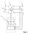
- the converter circuit comprises a converter unit 1 for switching at least two switching voltage levels. On the alternating voltage side, the converter unit 1 is connected to an electrical alternating voltage network 2. Furthermore, a capacitive energy store 3 is connected to the converter unit 1, which is typically formed by one or more capacitors.
- a drive device 4 is provided, which in terms of method drives the controllable power semiconductor switches by means of a drive signal S during operation of the converter circuit.
- the drive signal S is typically formed from reference voltages u * Na , u * Nb , u * Nc , wherein an allocation unit 6 is provided for forming the drive signal S, which assigns corresponding drive signal values to the reference voltages u * Na , u * Nb , U * Nc .
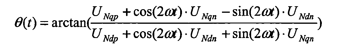
- the reference voltages u * Na , u * Nb , u * Nc are formed from a periodic modulation index m (t) and from a periodic modulation angle ⁇ (t). Accordingly, both the periodic modulation index m (t) and the periodic modulation angle ⁇ (t) is a function of the time t and thus, in particular, time-dependent.
- the periodic modulation index m (t) and the periodic modulation angle ⁇ (t) become respectively from the d-component of the Park-Clarke transformation of the positive sequence of the phase voltages U Ndp , from the q-component of the Park-Clarke transformation of the positive sequence the phase voltages U Nqp , the d-component of the Park-Clarke transformation of the negative sequence of the phase voltages U Ndn and the q-component of the Park-Clarke transformation of the negative sequence of the phase voltages U Nqn .
- the reference voltages u * Na , u * Nb , u * Nc are formed only from one, in particular from a single, periodic modulation index m (t) and one, in particular from a single, periodic modulation angle ⁇ (t) and the periodic modulation index m (t) and also the periodic modulation angle ⁇ (t) in each case from the d-component of the Park-Clarke transformation the positive sequence of the phase voltages U Ndp , from the q component of the Park-Clarke transformation of the positive sequence of the phase voltages U Nqp , d component of the Park-Clarke transformation of the negative sequence of the phase voltages U Ndn and from the q component the Park-Clarke transformation of the negative sequence of the phase voltages U Nqn is formed, advantageously only a very small computational effort is necessary to form the reference voltages u * Na, u * Nb , U * Nc .
- the converter circuit can be operated very simply and efficiently with the method according to the invention, and furthermore a low susceptibility to error and thus a high availability of the converter circuit can be achieved along with a low maintenance requirement.
- three independent constant modulation indices and three independent constant modulation angles no longer need to be formed, for example, in a three-phase AC electrical network, but only a periodic modulation index m (t) and a periodic modulation angle ⁇ (t).
- the converter unit 1 preferably follows the phase voltages U Na , U Nb , U Nc , in particular even if asymmetrical phase voltages U Na , U Nb , U Nc are present, ie the reference voltages u * Na , u * Nb , u * Nc correspond to the phase voltages U Na , U Nb , U Nc .
- the reference voltages u * Na , u * Nb , u * Nc are formed in particular in the drive device 4, in particular by calculation.
- the d-component of the Park-Clarke transformation of the phase voltages U Nd and the q-component of the Park-Clarke transformation of the phase voltages U Nq is, in particular in the control device 4, from the determined phase voltages U Na , U Nb , U Nc , in particular by calculation, wherein the d-component of the Park-Clarke transformation of the phase voltages U Nd and the q-component of the Park-Clarke transformation of the phase voltages U Nq then, as already explained above, to form the d-component the Park-Clarke transformation of the positive sequence of the phase voltages U Ndp , the q component of the Park-Clarke transformation of the positive sequence of the phase voltages U Nqp , the d component of the Park-Clarke transformation of the negative sequence of the phase voltages U Ndn and the q-component of the Park-Clarke transformation of the negative sequence of the phase voltages U Nqn be used.
- the positive sequence of the phase voltages U Np have positive coordinate positive coordinates and an angular velocity w and the negative sequence of the phase voltages U Nn have positive coordinates in the negative reference frame and an angular velocity - ⁇ .
- the formation of the reference voltages u * Na , u * Nb , u * Nc , the formation of the periodic modulation index m (t) and the formation of the periodic modulation angle ⁇ (t) preferably takes place continuously, whereby always the most recent values of the reference voltages u * Na , u * Nb , u * Nc , the periodic modulation index m (t) and the periodic modulation angle ⁇ (t).
- the formation of the d-component of the Park-Clarke transformation of the positive sequence of the phase voltages U Ndp , the formation of the q-component of the Park-Clarke transformation of the positive sequence of the phase voltages U Nqp , the formation of the d-component of the Park Clarke transformation of the negative sequence of the phase voltages U Ndn and the formation of the q-component of the Park-Clarke transformation of the negative sequence of the phase voltages U Nqn preferably takes place continuously. Furthermore, the determination of the phase voltages U Na , U Nb , U Nc of the alternating voltage network 2 is carried out continuously, so that it is always possible to calculate with the most recent values.
- the formation of the d-component of the Park-Clarke transformation of the phase voltages U Nd and the formation of the q-component of the Park-Clarke transformation of the phase voltages U N q preferably likewise take place continuously.
Abstract
Description
Die Erfindung bezieht sich auf das Gebiet der Leistungselektronik. Sie geht aus von einem Verfahren zum Betrieb einer Umrichterschaltung gemäss dem Oberbegriff des unabhängigen Anspruchs.The invention relates to the field of power electronics. It is based on a method for operating a converter circuit according to the preamble of the independent claim.
Herkömmliche Umrichterschaltungen umfassen eine Umrichtereinheit mit einer Vielzahl an ansteuerbaren Leistungshalbleiterschaltern, welche in bekannter Weise zur Schaltung von mindestens zwei Schaltspannungsniveaus verschaltet sind. Wechselspannungsseitig ist die Umrichtereinheit mit einem elektrischen Wechselspannungsnetz verbunden. Ferner ist ein kapazitiver Energiespeicher mit der Umrichtereinheit verbunden, welcher gängigerweise durch einen oder mehrere Kondensatoren gebildet ist. Für den Betrieb der Umrichterschaltung ist eine Ansteuervorrichtung vorgesehen, welche verfahrensmässig beim Betrieb der Umrichterschaltung die ansteuerbaren Leistungshalbleiterschalter mittels eines Ansteuersignals angesteuert. Das Ansteuersignal wird typischerweise aus Referenzspannungen gebildet, wobei zur Bildung des Ansteuersignals eine Zuordnungseinheit vorgesehen ist, welche den Referenzspannungen entsprechende Ansteuersignalwerte zugeordnet. Die entsprechende Referenzspannung ist die Spannung, die am zugehörigen Phasenausgang der Umrichtereinheit von der Umrichtereinheit eingestellt wird und entspricht typischerweise der zugehörigen Phasenspannung, so dass die Umrichtereinheit an ihren Phasenausgängen Spannungen entsprechend den Phasenspannungen des elektrischen Wechselspannungsnetzes einstellt. Dabei ist es unerheblich, ob symmetrische oder unsymmetrische Phasenspannungen vorliegen. Unsymmetrische Phasenspannungen liegen beispielsweise bei unterschiedlichen Phasenwinkeln der Phasenspannungen zueinander und/oder bei unterschiedlichen Amplituden der Phasenspannungen zueinander und/oder bei unterschiedlichen Frequenzen der Phasenspannungen zueinander vor. Jede Referenzspannung wird gemäss dem Stand der Technik aus einem ihr zugeordneten konstanten Modulationsindex und einem ihr zugeordneten konstanten Modulationswinkel gebildet. Somit sind beispielsweise bei einem dreiphasigen elektrischen Wechselspannungsnetz mit drei Phasenspannungen auch drei Referenzspannungen notwendig und damit auch drei unabhängige konstante Modulationsindexe sowie drei unabhängige konstante Modulationswinkel, wobei diese konstanten Modulationsindexe und diese konstanten Modulationswinkel typischerweise durch Berechnung gebildet werden, wodurch ein enormer Rechenaufwand entsteht. Demzufolge ist der Betrieb der Umrichterschaltung sehr aufwendig, uneffizient, teuer und fehleranfällig, wodurch die Verfügbarkeit der Umrichterschaltung massiv sinkt und sich die Wartung der Umrichterschaltung signifikant erhöht.Conventional converter circuits comprise a converter unit with a plurality of controllable power semiconductor switches, which are connected in a known manner for switching at least two switching voltage levels. On the alternating voltage side, the converter unit is connected to an electrical alternating voltage network. Furthermore, a capacitive energy store is connected to the converter unit, which is usually formed by one or more capacitors. For the operation of the converter circuit, a drive device is provided which, in terms of method, drives the controllable power semiconductor switches by means of a drive signal during operation of the converter circuit. The drive signal is typically formed from reference voltages, wherein an allocation unit is provided for forming the drive signal, which assigns drive signal values corresponding to the reference voltages. The corresponding reference voltage is the voltage at the associated phase output of the inverter unit is adjusted by the inverter unit and typically corresponds to the associated phase voltage, so that the converter unit adjusts voltages at their phase outputs according to the phase voltages of the AC electrical network. It is irrelevant whether symmetrical or asymmetrical phase voltages are present. Unbalanced phase voltages are present, for example, at different phase angles of the phase voltages to one another and / or at different amplitudes of the phase voltages relative to one another and / or at different frequencies of the phase voltages relative to one another. Each reference voltage is formed according to the prior art from a constant modulation index associated with it and a constant modulation angle associated therewith. Thus, for example, in a three-phase AC electrical network with three phase voltages and three reference voltages are necessary and thus three independent constant modulation indexes and three independent constant modulation angle, these constant modulation indexes and these constant modulation angles are typically formed by calculation, creating a huge computational burden. Consequently, the operation of the converter circuit is very expensive, inefficient, expensive and error-prone, whereby the availability of the converter circuit drops massively and the maintenance of the converter circuit increases significantly.
Aufgabe der Erfindung ist es deshalb, ein Verfahren zum Betrieb einer Umrichterschaltung anzugeben, mittels welchem die Umrichterschaltung sehr einfach und effizient betrieben werden kann.The object of the invention is therefore to provide a method for operating a converter circuit, by means of which the converter circuit can be operated very simply and efficiently.
Beim erfindungsgemässen Verfahren zum Betrieb einer Umrichterschaltung weist die Umrichterschaltung eine Umrichtereinheit mit einer Vielzahl an ansteuerbaren Leistungshalbleiterschaltern auf, wobei die Umrichtereinheit wechselspannungsseitig mit einem elektrischen Wechselspannungsnetz verbunden ist und die ansteuerbaren Leistungshalbleiterschalter mittels eines aus Referenzspannungen gebildeten Ansteuersignals angesteuert werden. Erfindungsgemäss werden die Referenzspannungen aus einem periodischen Modulationsindex und aus einem periodischen Modulationswinkel gebildet, wobei der periodischen Modulationsindex und der periodischen Modulationswinkel jeweils aus der d-Komponente der Park-Clarke-Transformation der positive Sequenz der Phasenspannungen, aus der q-Komponente der Park-Clarke-Transformation der positive Sequenz der Phasenspannungen, aus d-Komponente der Park-Clarke-Transformation der negativen Sequenz der Phasenspannungen und aus der q-Komponente der Park-Clarke-Transformation der negativen Sequenz der Phasenspannungen gebildet wird. Dadurch, dass die Referenzspannungen lediglich aus einem, insbesondere aus einem einzigen, periodische Modulationsindex sowie aus einem, insbesondere aus einem einzigen, periodischen Modulationswinkel gebildet werden, welcher periodische Modulationsindex und periodische Modulationswinkel jeweils aus der d-Komponente der Park-Clarke-Transformation der positive Sequenz der Phasenspannungen, aus der q-Komponente der Park-Clarke-Transformation der positive Sequenz der Phasenspannungen, aus d-Komponente der Park-Clarke-Transformation der negativen Sequenz der Phasenspannungen und aus der q-Komponente der Park-Clarke-Transformation der negativen Sequenz der Phasenspannungen gebildet wird, ist mit Vorteil nur ein sehr geringer Rechenaufwand zur Bildung der Referenzspannungen notwendig. Die Umrichterschaltung lässt sich mit dem erfindungsgemässen Verfahren somit besonders einfach und effizient betreiben, wobei zudem eine geringe Fehleranfälligkeit und damit eine hohe Verfügbarkeit der Umrichterschaltung einhergehend mit einem geringen Wartungsaufwand erreicht werden kann.In the method according to the invention for operating a converter circuit, the converter circuit has an inverter unit with a large number of controllable power semiconductor switches, the inverter unit being connected to an alternating voltage network on the alternating voltage side and the controllable power semiconductor switches being actuated by means of a drive signal formed from reference voltages. According to the invention, the reference voltages are formed from a periodic modulation index and from a periodic modulation angle, the periodic modulation index and the periodic modulation angle respectively from the d-component of the Park-Clarke transformation of the positive sequence of the phase voltages, from the q-component of the Park-Clarke transformation of the positive sequence of the phase voltages, from the d-component of the Park-Clarke transformation negative sequence of the phase voltages and from the q-component of the Park-Clarke transformation of the negative sequence of the phase voltages is formed. By virtue of the fact that the reference voltages are formed only from one, in particular from a single, periodic modulation index and from one, in particular from a single, periodic modulation angle, which periodic modulation index and periodic modulation angle each from the d-component of the Park-Clarke transformation Sequence of phase voltages, from the q-component of the Park-Clarke transformation of the positive sequence of the phase voltages, from d-component of the Park-Clarke transformation of the negative sequence of the phase voltages and from the q-component of the Park-Clarke transformation of the negative Sequence of the phase voltages is formed, it is advantageous only a very low computational effort to form the reference voltages necessary. The converter circuit can thus be operated particularly simply and efficiently with the method according to the invention, wherein, in addition, a low susceptibility to errors and thus a high availability of the converter circuit can be achieved along with a low level of maintenance.
Diese und weitere Aufgaben, Vorteile und Merkmale der vorliegenden Erfindung werden aus der nachfolgenden detaillierten Beschreibung bevorzugter Ausführungsformen der Erfindung in Verbindung mit der Zeichnung offensichtlich.These and other objects, advantages and features of the present invention will become more apparent from the following detailed description of preferred embodiments of the invention taken in conjunction with the accompanying drawings.
Es zeigt:
- Fig. 1
- eine Ausführungsform einer Umrichterschaltung, welche mit dem erfindungsgemässen Verfahren betrieben wird.
- Fig. 1
- an embodiment of a converter circuit which is operated by the inventive method.
Die in der Zeichnung verwendeten Bezugszeichen und deren Bedeutung sind in der Bezugszeichenliste zusammengefasst aufgelistet. Grundsätzlich sind in der Figur gleiche Teile mit gleichen Bezugszeichen versehen. Die beschriebene Ausführungsform ist als Beispiel zu verstehen hat keine beschränkende Wirkung.The reference numerals used in the drawings and their meaning are listed in the list of reference numerals. Basically, the same parts in the figure with provided the same reference numerals. The described embodiment is to be understood as an example has no limiting effect.
Eine gängige Ausführungsform einer Umrichterschaltung ist in Fig. 1 gezeigt. Die Umrichterschaltung umfasst eine Umrichtereinheit 1 zur Schaltung von mindestens zwei Schaltspannungsniveaus. Wechselspannungsseitig ist die Umrichtereinheit 1 mit einem elektrischen Wechselspannungsnetz 2 verbunden. Desweiteren ist ein kapazitiver Energiespeicher 3 mit der Umrichtereinheit 1 verbunden, welcher typischerweise durch einen oder mehrere Kondensatoren gebildet ist. Für den Betrieb der Umrichterschaltung ist eine Ansteuervorrichtung 4 vorgesehen, welche verfahrensmässig beim Betrieb der Umrichterschaltung die ansteuerbaren Leistungshalbleiterschalter mittels eines Ansteuersignals S angesteuert. Das Ansteuersignal S wird typischerweise aus Referenzspannungen u*Na, u*Nb, u*Nc gebildet, wobei zur Bildung des Ansteuersignals S eine Zuordnungseinheit 6 vorgesehen ist, welche den Referenzspannungen u*Na, u*Nb, U*Nc entsprechende Ansteuersignalwerte zugeordnet.A common embodiment of a converter circuit is shown in FIG. The converter circuit comprises a
Bezüglich des erfindungsgemässen Verfahrens zum Betrieb einer solchen Umrichterschaltung werden die Referenzspannungen u*Na, u*Nb, u*Nc aus einem periodischen Modulationsindex m(t) und aus einem periodischen Modulationswinkel θ(t) gebildet. Demnach ist sowohl der periodische Modulationsindex m(t) als auch der periodische Modulationswinkel θ(t) eine Funktion der Zeit t und damit insbesondere zeitabhängig. Der periodische Modulationsindex m(t) und der periodische Modulationswinkel θ(t) wird jeweils aus der d-Komponente der Park-Clarke-Transformation der positive Sequenz der Phasenspannungen UNdp, aus der q-Komponente der Park-Clarke-Transformation der positive Sequenz der Phasenspannungen UNqp, aus d-Komponente der Park-Clarke-Transformation der negativen Sequenz der Phasenspannungen UNdn und aus der q-Komponente der Park-Clarke-Transformation der negativen Sequenz der Phasenspannungen UNqn gebildet. Dadurch, dass die Referenzspannungen u*Na, u*Nb, u*Nc lediglich aus einem, insbesondere aus einem einzigen, periodische Modulationsindex m(t) sowie aus einem, insbesondere aus einem einzigen, periodischen Modulationswinkel θ(t) gebildet werden und der periodische Modulationsindex m(t) und auch der periodischen Modulationswinkel θ(t) jeweils aus der d-Komponente der Park-Clarke-Transformation der positive Sequenz der Phasenspannungen UNdp, aus der q-Komponente der Park-Clarke-Transformation der positive Sequenz der Phasenspannungen UNqp, aus d-Komponente der Park-Clarke-Transformation der negativen Sequenz der Phasenspannungen UNdn und aus der q-Komponente der Park-Clarke-Transformation der negativen Sequenz der Phasenspannungen UNqn gebildet wird, ist vorteilhaft nur ein sehr geringer Rechenaufwand zur Bildung der Referenzspannungen u*Na, u*Nb, U*Nc notwendig. Die Umrichterschaltung lässt sich mit dem erfindungsgemässen Verfahren demzufolge sehr einfach und effizient betreiben, wobei ferner eine geringe Fehleranfälligkeit und damit eine hohe Verfügbarkeit der Umrichterschaltung einhergehend mit einem geringen Wartungsaufwand erreicht werden kann. Gegenüber dem Stand der Technik müssen beispielsweise bei einem dreiphasigen elektrischen Wechselspannungsnetz nicht mehr drei unabhängige konstante Modulationsindexe sowie drei unabhängige konstante Modulationswinkel gebildet werden sonder lediglich nur noch ein periodischer Modulationsindex m(t) und ein periodischer Modulationswinkel θ(t).With regard to the method according to the invention for operating such a converter circuit, the reference voltages u * Na , u * Nb , u * Nc are formed from a periodic modulation index m (t) and from a periodic modulation angle θ (t). Accordingly, both the periodic modulation index m (t) and the periodic modulation angle θ (t) is a function of the time t and thus, in particular, time-dependent. The periodic modulation index m (t) and the periodic modulation angle θ (t) become respectively from the d-component of the Park-Clarke transformation of the positive sequence of the phase voltages U Ndp , from the q-component of the Park-Clarke transformation of the positive sequence the phase voltages U Nqp , the d-component of the Park-Clarke transformation of the negative sequence of the phase voltages U Ndn and the q-component of the Park-Clarke transformation of the negative sequence of the phase voltages U Nqn . The fact that the reference voltages u * Na , u * Nb , u * Nc are formed only from one, in particular from a single, periodic modulation index m (t) and one, in particular from a single, periodic modulation angle θ (t) and the periodic modulation index m (t) and also the periodic modulation angle θ (t) in each case from the d-component of the Park-Clarke transformation the positive sequence of the phase voltages U Ndp , from the q component of the Park-Clarke transformation of the positive sequence of the phase voltages U Nqp , d component of the Park-Clarke transformation of the negative sequence of the phase voltages U Ndn and from the q component the Park-Clarke transformation of the negative sequence of the phase voltages U Nqn is formed, advantageously only a very small computational effort is necessary to form the reference voltages u * Na, u * Nb , U * Nc . Consequently, the converter circuit can be operated very simply and efficiently with the method according to the invention, and furthermore a low susceptibility to error and thus a high availability of the converter circuit can be achieved along with a low maintenance requirement. Compared to the prior art, three independent constant modulation indices and three independent constant modulation angles no longer need to be formed, for example, in a three-phase AC electrical network, but only a periodic modulation index m (t) and a periodic modulation angle θ (t).
Der periodische Modulationsindex m(t) und der periodische Modulationswinkel θ(t) werden insbesondere in der Ansteuervorrichtung 4 wie folgt, insbesondere durch Berechnung, gebildet 
wobei UDC die Spannung am kapazitiven Energiespeicher 3 ist und wobei ω=2ΠFnom ist und Fnom die Nominalfrequenz des elektrischen Wechselspannungsnetzes 2 ist, beispielsweise Fnom=50 Hz bei einem gängigen elektrischen Verbundwechselspannungsnetz oder Fnom=16 2/3Hz bei einem elektrischen Bahnwechselspannungsnetz. Zur Ermittlung des Phasenwinkels ωt umfasst die Ansteuervorrichtung 4 vorzugsweise einen Phasenregelkreis (Phase locked loop).The periodic modulation index m (t) and the periodic modulation angle θ (t) are formed in particular in the
wherein U DC is the voltage at the
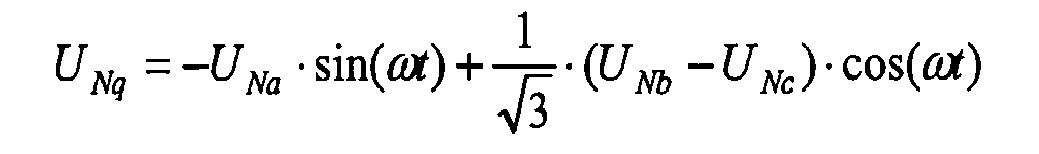
Vorzugsweise folgt die Umrichtereinheit 1 den Phasenspannungen UNa, UNb, UNc, insbesondere auch wenn unsymmetrische Phasenspannungen UNa, UNb, UNc vorliegen, d.h. die Referenzspannungen u*Na, u*Nb, u*Nc entsprechen den Phasenspannungen UNa, UNb, UNc. Im Park-Clarke-Bezugssystem (dq-Bezugssystem) ergibt sich die d-Komponente der Park-Clarke-Transformation der Referenzspannungen u*d und die q-Komponente der Park-Clarke-Transformation der der Referenzspannungen u*q zu ![]()
![]()
![]()
![]()
Mittels der inversen Park-Clarke-Transformation, d.h. durch die Rücktransformation in den Zeitbereich ergeben sich dann die Referenzspannungen u*Na, u*Nb, u*Nczu ![]()


![]()
Die Referenzspannungen u*Na, u*Nb, u*Nc werden insbesondere in der Ansteuervorrichtung 4, insbesondere durch Berechnung, gebildet.The reference voltages u * Na , u * Nb , u * Nc are formed in particular in the
Vorzugsweise wird die d-Komponente der Park-Clarke-Transformation der positive Sequenz der Phasenspannungen UNdp, die q-Komponente der Park-Clarke-Transformation der positive Sequenz der Phasenspannungen UNqp, die d-Komponente der Park-Clarke-Transformation der negativen Sequenz der Phasenspannungen UNdn und die q-Komponente der Park-Clarke-Transformation der negativen Sequenz der Phasenspannungen UNqn jeweils aus der d-Komponente der Park-Clarke-Transformation der Phasenspannungen UNd und aus der q-Komponente der Park-Clarke-Transformation der Phasenspannungen UNq gebildet. Die Bildung erfolgt insbesondere in der Ansteuervorrichtung 4 und insbesondere durch Berechnung wie folgt 
![]()
![]()
![]()

wobei UNdt1 die um die Zeitdauer t1 verzögerte d-Komponente der Park-Clarke-Transformation der Phasenspannungen UNd ist und UNqt1 die um die Zeitdauer t1 verzögerte q-Komponente der Park-Clarke-Transformation der Phasenspannungen UNq ist. Vorzugsweise wird die Zeitdauer t1 in der Grössenordnung von 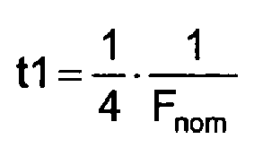
![]()
![]()
![]()
where U Ndt1 is the d-component of the Park-Clarke transformation of the phase voltages U Nd delayed by the time t1, and U Nqt1 is the q-component of the Park-Clarke transformation of the phase voltages U Nq delayed by the time t1. Preferably, the time t1 is of the order of
Der Vollständigkeit halber sei erwähnt, dass insbesondere im Falle von unsymmetrischen Phasenspannungen UNa, UNb, UNc diese unsymmetrischen Phasenspannungen UNa, UNb, UNc in eine positive Sequenz der Phasenspannungen UNp (positives Bezugssystem) und in eine negative Sequenz der Phasenspannungen UNn (negatives Bezugssystem) zerlegt werden können, die sich dann allgemein wie folgt ergeben zu ![]()
![]()
![]()
![]()
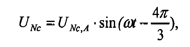
Die Phasenspannungen UNa, UNb, UNc selbst sind wie folgt definiert: ![]()
![]()
wobei die Phasenspannungen UNa, UNb, UNc des Wechselspannungsnetzes 2, insbesondere durch Messung, ermittelt werden und die Summe der Phasenspannungen UNa, UNb, UNc Null ergibt, d.h. es gilt ![]()
![]()
![]()
wherein the phase voltages U Na , U Nb , U Nc of the ![]()
Die d-Komponente der Park-Clarke-Transformation der Phasenspannungen UNd und die q-Komponente der Park-Clarke-Transformation der Phasenspannungen UNq ergeben sich dann zu 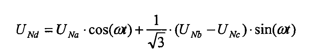
Die d-Komponente der Park-Clarke-Transformation der Phasenspannungen UNd und die q-Komponente der Park-Clarke-Transformation der Phasenspannungen UNq, wird, insbesondere in der Ansteuervorrichtung 4, aus den ermittelten Phasenspannungen UNa, UNb, UNc, insbesondere durch Berechnung, gebildet, wobei die d-Komponente der Park-Clarke-Transformation der Phasenspannungen UNd und der q-Komponente der Park-Clarke-Transformation der Phasenspannungen UNq dann, wie vorstehend bereits erläutert, zur Bildung der d-Komponente der Park-Clarke-Transformation der positive Sequenz der Phasenspannungen UNdp, der q-Komponente der Park-Clarke-Transformation der positive Sequenz der Phasenspannungen UNqp, der d-Komponente der Park-Clarke-Transformation der negativen Sequenz der Phasenspannungen UNdn und der q-Komponente der Park-Clarke-Transformation der negativen Sequenz der Phasenspannungen UNqn herangezogen werden.The d-component of the Park-Clarke transformation of the phase voltages U Nd and the q-component of the Park-Clarke transformation of the phase voltages U Nq is, in particular in the
Es sei an dieser Stelle angemerkt, dass die positive Sequenz der Phasenspannungen UNp positive Koordinaten im positiven Bezugssystemen und eine Winkelgeschwindigkeit w und die negative Sequenz der Phasenspannungen UNn positive Koordinaten im negativen Bezugssystemen und eine Winkelgeschwindigkeit -ω aufweist.
Mit der positive Sequenz der Phasenspannungen UNp und der negativen Sequenz der Phasenspannungen UNn kann die Gesamtphasenspannung ![]()
im positive Bezugssystem mit der d-Komponente der Park-Clarke-Transformation der Phasenspannungen UNd und der q-Komponente der Park-Clarke-Transformation der Phasenspannungen UNq wie folgt geschrieben werden 
wobei der Term ![]()
die Koordinaten der negative Sequenz der Phasenspannungen UNn im positiven Bezugssystem sind, welche mit einer 2-fachen Winkelgeschwindigkeit ω rotieren.It should be noted at this point that the positive sequence of the phase voltages U Np have positive coordinate positive coordinates and an angular velocity w and the negative sequence of the phase voltages U Nn have positive coordinates in the negative reference frame and an angular velocity -ω.
With the positive sequence of the phase voltages U Np and the negative sequence of the phase voltages U Nn , the total phase voltage ![]()
in the positive frame of reference with the d-component of the Park-Clarke transformation of the phase voltages U Nd and the q-component of the Park-Clarke transformation of the phase voltages U Nq are written as follows
where the term ![]()
are the coordinates of the negative sequence of the phase voltages U Nn in the positive reference frame, which rotate at a 2-fold angular velocity ω.
Die Bildung der Referenzspannungen u*Na, u*Nb, u*Nc, die Bildung des periodischen Modulationsindexes m(t) und die Bildung des periodischen Modulationswinkels θ(t) erfolgt vorzugsweise fortlaufend, wodurch immer die aktuellsten Werte der Referenzspannungen u*Na, u*Nb, u*Nc, des periodischen Modulationsindexes m(t) und des periodischen Modulationswinkels θ(t) vorliegen. Auch die Bildung der d-Komponente der Park-Clarke-Transformation der positive Sequenz der Phasenspannungen UNdp, die Bildung der q-Komponente der Park-Clarke-Transformation der positive Sequenz der Phasenspannungen UNqp, die Bildung der d-Komponente der Park-Clarke-Transformation der negativen Sequenz der Phasenspannungen UNdn und die Bildung der q-Komponente der Park-Clarke-Transformation der negativen Sequenz der Phasenspannungen UNqn erfolgt vorzugsweise fortlaufend. Weiterhin erfolgt die Ermittlung der Phasenspannungen UNa, UNb, UNc des Wechselspannungsnetzes 2 fortlaufend, so dass stets mit aktuellsten Werten gerechnet werden kann. Ferner erfolgt die Bildung der d-Komponente der Park-Clarke-Transformation der Phasenspannungen UNd und die Bildung der q-Komponente der Park-Clarke-Transformation der Phasenspannungen UNq vorzugsweise ebenfalls fortlaufend.The formation of the reference voltages u * Na , u * Nb , u * Nc , the formation of the periodic modulation index m (t) and the formation of the periodic modulation angle θ (t) preferably takes place continuously, whereby always the most recent values of the reference voltages u * Na , u * Nb , u * Nc , the periodic modulation index m (t) and the periodic modulation angle θ (t). The formation of the d-component of the Park-Clarke transformation of the positive sequence of the phase voltages U Ndp , the formation of the q-component of the Park-Clarke transformation of the positive sequence of the phase voltages U Nqp , the formation of the d-component of the Park Clarke transformation of the negative sequence of the phase voltages U Ndn and the formation of the q-component of the Park-Clarke transformation of the negative sequence of the phase voltages U Nqn preferably takes place continuously. Furthermore, the determination of the phase voltages U Na , U Nb , U Nc of the alternating
- 11
- Umrichtereinheitinverter unit
- 22
- elektrisches Wechselspannungsnetzelectric alternating voltage network
- 33
- kapazitiver Energiespeichercapacitive energy storage
- 44
- Ansteuervorrichtungdriving
- 55
- Berechnungseinheitcalculation unit
- 66
- Zuordnungseinheitallocation unit
Claims (6)
bei dem die ansteuerbaren Leistungshalbleiterschalter mittels eines aus Referenzspannungen (u*Na, u*Nb, u*Nc) gebildeten Ansteuersignals (S) angesteuert werden,
dadurch gekennzeichnet,
dass die Referenzspannungen (u*Na, u*Nb, u*Nc) aus einem periodischen Modulationsindex (m(t)) und aus einem periodischen Modulationswinkel (θ(t)) gebildet werden,
und
dass der periodischen Modulationsindex (m(t)) und der periodischen Modulationswinkel (θ(t)) jeweils aus der d-Komponente der Park-Clarke-Transformation der positive Sequenz der Phasenspannungen (UNdp), aus der q-Komponente der Park-Clarke-Transformation der positive Sequenz der Phasenspannungen (UNqp), aus d-Komponente der Park-Clarke-Transformation der negativen Sequenz der Phasenspannungen (UNdn) und aus der q-Komponente der Park-Clarke-Transformation der negativen Sequenz der Phasenspannungen (UNqn) gebildet wird.Method for operating a converter circuit, wherein the converter circuit has a converter unit (1) with a plurality of controllable power semiconductor switches, and the converter unit (1) is connected on the alternating voltage side to an electrical alternating voltage network (2),
in which the controllable power semiconductor switches are controlled by means of a drive signal (S) formed from reference voltages (u * Na , u * Nb , u * Nc ),
characterized,
that the reference voltages (u * Na, u * Nb, u * Nc) from a periodic modulation index (m (t)) and from a periodic modulation angle (θ (t)) are formed,
and
in that the periodic modulation index (m (t)) and the periodic modulation angle (θ (t)) are respectively derived from the d-component of the Park-Clarke transformation of the positive sequence of the phase voltages (U Ndp ), from the q-component of the parking Clarke transformation of the positive sequence of the phase voltages (U Nqp ), d component of the Park-Clarke transformation of the negative sequence of the phase voltages (U Ndn ) and the q component of the Park-Clarke transformation of the negative sequence of the phase voltages ( U Nqn ) is formed.
dass die d-Komponente der Park-Clarke-Transformation der Phasenspannungen (UNd) und die q-Komponente der Park-Clarke-Transformation der Phasenspannungen (UNq) aus den ermittelten Phasenspannungen (UNa, UNb, UNc) gebildet wird.A method according to claim 2 or 3, characterized in that the phase voltages (U Na , U Nb , U Nc ) of the alternating voltage network (2) are determined, and
the d component of the Park-Clarke transformation of the phase voltages (U Nd ) and the q component of the Park-Clarke transformation of the phase voltages (U Nq ) are formed from the determined phase voltages (U Na , U Nb , U Nc ) ,
dass die Bildung des periodischen Modulationsindexes (m(t)) und die Bildung des periodischen Modulationswinkels (θ(t)) fortlaufend erfolgt.Method according to one of claims 1 to 5, characterized in that the formation of the reference voltages (u * Na , u * Nb , u * Nc ) takes place continuously, and
the formation of the periodic modulation index (m (t)) and the formation of the periodic modulation angle (θ (t)) occur continuously.
Priority Applications (10)
| Application Number | Priority Date | Filing Date | Title |
|---|---|---|---|
| DE502006006244T DE502006006244D1 (en) | 2006-06-23 | 2006-06-23 | Method for operating a converter circuit |
| AT06405268T ATE459130T1 (en) | 2006-06-23 | 2006-06-23 | METHOD FOR OPERATING A CONVERTER CIRCUIT |
| EP06405268A EP1870997B1 (en) | 2006-06-23 | 2006-06-23 | Method of operating a converter circuit |
| KR1020137028286A KR20130127543A (en) | 2006-06-23 | 2007-06-12 | Method for operating a converter circuit |
| KR1020087031104A KR101435223B1 (en) | 2006-06-23 | 2007-06-12 | Method for operating a converter circuit |
| CN2007800234820A CN101479921B (en) | 2006-06-23 | 2007-06-12 | Method for operating a converter circuit |
| RU2009102078/09A RU2400915C1 (en) | 2006-06-23 | 2007-06-12 | Method of converting circuit operation |
| JP2009515825A JP5102291B2 (en) | 2006-06-23 | 2007-06-12 | Operation method of converter circuit |
| PCT/EP2007/055729 WO2007147747A2 (en) | 2006-06-23 | 2007-06-12 | Method for operating a converter circuit |
| US12/343,053 US7710749B2 (en) | 2006-06-23 | 2008-12-23 | Method for operating a converter circuit |
Applications Claiming Priority (1)
| Application Number | Priority Date | Filing Date | Title |
|---|---|---|---|
| EP06405268A EP1870997B1 (en) | 2006-06-23 | 2006-06-23 | Method of operating a converter circuit |
Publications (2)
| Publication Number | Publication Date |
|---|---|
| EP1870997A1 true EP1870997A1 (en) | 2007-12-26 |
| EP1870997B1 EP1870997B1 (en) | 2010-02-24 |
Family
ID=37499299
Family Applications (1)
| Application Number | Title | Priority Date | Filing Date |
|---|---|---|---|
| EP06405268A Not-in-force EP1870997B1 (en) | 2006-06-23 | 2006-06-23 | Method of operating a converter circuit |
Country Status (9)
| Country | Link |
|---|---|
| US (1) | US7710749B2 (en) |
| EP (1) | EP1870997B1 (en) |
| JP (1) | JP5102291B2 (en) |
| KR (2) | KR101435223B1 (en) |
| CN (1) | CN101479921B (en) |
| AT (1) | ATE459130T1 (en) |
| DE (1) | DE502006006244D1 (en) |
| RU (1) | RU2400915C1 (en) |
| WO (1) | WO2007147747A2 (en) |
Cited By (1)
| Publication number | Priority date | Publication date | Assignee | Title |
|---|---|---|---|---|
| EP2093875A1 (en) * | 2008-02-22 | 2009-08-26 | ABB Schweiz AG | Method for operating an inverter controller and device for carrying out the method |
Families Citing this family (4)
| Publication number | Priority date | Publication date | Assignee | Title |
|---|---|---|---|---|
| ES2333996T3 (en) * | 2008-03-19 | 2010-03-03 | Abb Schweiz Ag | METHOD FOR THE PERFORMANCE OF A CONVERTER CIRCUIT, AS WELL AS DEVICE FOR THE PERFORMANCE OF THE METHOD. |
| ES2595374T3 (en) * | 2009-09-24 | 2016-12-29 | Vestas Wind Systems A/S | Method to control a power converter in a wind turbine generator |
| CN102680806A (en) * | 2012-04-20 | 2012-09-19 | 京东方科技集团股份有限公司 | Detection method and detection device for three-phase alternating-current phase sequence |
| CN102981068B (en) * | 2012-12-02 | 2015-09-09 | 威海广泰空港设备股份有限公司 | A kind of phase sequence detecting method of three-phase grid photovoltaic DC-to-AC converter |
Citations (2)
| Publication number | Priority date | Publication date | Assignee | Title |
|---|---|---|---|---|
| US6052297A (en) * | 1998-05-06 | 2000-04-18 | Mitsubishi Denki Kabushiki Kaisha | Power conversion apparatus |
| US6201715B1 (en) * | 2000-03-28 | 2001-03-13 | Honeywell International Inc. | Synchronous frame regulation to extract a positive sequence component of a line voltage |
Family Cites Families (3)
| Publication number | Priority date | Publication date | Assignee | Title |
|---|---|---|---|---|
| JP2000116148A (en) * | 1998-02-13 | 2000-04-21 | Mitsubishi Electric Corp | Power conversion apparatus |
| US6847194B2 (en) * | 2002-09-20 | 2005-01-25 | Honeywell International Inc. | Electric start for a prime mover |
| US7136733B2 (en) * | 2003-08-28 | 2006-11-14 | Motorola, Inc. | Fault detection in an electric power-assisted steering system |
-
2006
- 2006-06-23 DE DE502006006244T patent/DE502006006244D1/en active Active
- 2006-06-23 AT AT06405268T patent/ATE459130T1/en active
- 2006-06-23 EP EP06405268A patent/EP1870997B1/en not_active Not-in-force
-
2007
- 2007-06-12 WO PCT/EP2007/055729 patent/WO2007147747A2/en active Application Filing
- 2007-06-12 CN CN2007800234820A patent/CN101479921B/en not_active Expired - Fee Related
- 2007-06-12 JP JP2009515825A patent/JP5102291B2/en not_active Expired - Fee Related
- 2007-06-12 KR KR1020087031104A patent/KR101435223B1/en active IP Right Grant
- 2007-06-12 KR KR1020137028286A patent/KR20130127543A/en not_active Application Discontinuation
- 2007-06-12 RU RU2009102078/09A patent/RU2400915C1/en not_active IP Right Cessation
-
2008
- 2008-12-23 US US12/343,053 patent/US7710749B2/en not_active Expired - Fee Related
Patent Citations (2)
| Publication number | Priority date | Publication date | Assignee | Title |
|---|---|---|---|---|
| US6052297A (en) * | 1998-05-06 | 2000-04-18 | Mitsubishi Denki Kabushiki Kaisha | Power conversion apparatus |
| US6201715B1 (en) * | 2000-03-28 | 2001-03-13 | Honeywell International Inc. | Synchronous frame regulation to extract a positive sequence component of a line voltage |
Cited By (3)
| Publication number | Priority date | Publication date | Assignee | Title |
|---|---|---|---|---|
| EP2093875A1 (en) * | 2008-02-22 | 2009-08-26 | ABB Schweiz AG | Method for operating an inverter controller and device for carrying out the method |
| US8045347B2 (en) | 2008-02-22 | 2011-10-25 | Abb Schweiz Ag | Method for operating a converter circuit, and apparatus for carrying out the method |
| RU2478253C2 (en) * | 2008-02-22 | 2013-03-27 | Абб Швайц Аг | Operation method of converter diagram, and device for method's implementation |
Also Published As
| Publication number | Publication date |
|---|---|
| RU2400915C1 (en) | 2010-09-27 |
| WO2007147747A3 (en) | 2008-04-17 |
| JP2009542172A (en) | 2009-11-26 |
| US20090147540A1 (en) | 2009-06-11 |
| EP1870997B1 (en) | 2010-02-24 |
| KR20130127543A (en) | 2013-11-22 |
| RU2009102078A (en) | 2010-07-27 |
| WO2007147747A2 (en) | 2007-12-27 |
| KR101435223B1 (en) | 2014-08-28 |
| KR20090021354A (en) | 2009-03-03 |
| DE502006006244D1 (en) | 2010-04-08 |
| JP5102291B2 (en) | 2012-12-19 |
| US7710749B2 (en) | 2010-05-04 |
| CN101479921A (en) | 2009-07-08 |
| ATE459130T1 (en) | 2010-03-15 |
| CN101479921B (en) | 2013-03-27 |
Similar Documents
| Publication | Publication Date | Title |
|---|---|---|
| EP1870991A1 (en) | Method for operating an inverter circuit | |
| EP1842283B1 (en) | Method and device for the operation of a converter circuit comprising an lcl filter | |
| EP1842281B1 (en) | Method and device for the operation of a converter circuit comprising an lcl filter | |
| EP1759450B1 (en) | Low harmonic multiphase converter circuit | |
| DE102020117435B3 (en) | Method for compensating for phase voltage imbalances | |
| EP1870997B1 (en) | Method of operating a converter circuit | |
| EP3870982A1 (en) | Method for measuring insulation resistance in inverters with multipoint topology, and inverter with multipoint topology | |
| EP1211797B1 (en) | Reduction of self-oscillation in an intermediate electric circuit driven by a voltage-controlled, mains-connected intermediate circuit and corresponding voltage-controlled inverter | |
| EP2283572B1 (en) | Open-loop or closed-loop control method for a converter | |
| EP1952522B1 (en) | Method for operating a converter circuit and device for carrying out the method | |
| EP4046268B1 (en) | Determination of filter parameters within an inverter | |
| DE102021133236A1 (en) | METHOD AND DEVICE FOR GENERATION OF A THREE-PHASE VOLTAGE | |
| DE102021100922B4 (en) | Method for determining a gliding current value describing a direct current in an inverter, inverter arrangement and motor vehicle | |
| DE102009049934B4 (en) | From an electric AC power supplyable electrical device and method for fault detection | |
| EP1513249B1 (en) | Method for neutral-point balancing of a three-level inverter | |
| EP2254233B1 (en) | Method for operating an inverter controller and device for carrying out the method | |
| WO2019137581A1 (en) | Method and device for monitoring a power electronic assembly | |
| EP3556003B1 (en) | Multi-level converter and method for operating the same | |
| EP2409394B1 (en) | Method for operating an inverter circuit and device for performing the method | |
| EP2274827B1 (en) | Method for operating a converter circuit, and apparatus for carrying out the method | |
| DE102015008369A1 (en) | Circuit arrangement for the bidirectional coupling of a DC voltage system with a plurality of AC systems and method for controlling such a circuit arrangement | |
| DE102019217747A1 (en) | Detecting an inverter short circuit between two phases | |
| EP1298781B1 (en) | Power converter device and method for adjusting a variable DC voltage | |
| DE2018060A1 (en) | Method and device for displaying the angular adjustment of the rotor of a synchronous encoder or resolver about an axis | |
| EP2093875A1 (en) | Method for operating an inverter controller and device for carrying out the method |
Legal Events
| Date | Code | Title | Description |
|---|---|---|---|
| PUAI | Public reference made under article 153(3) epc to a published international application that has entered the european phase |
Free format text: ORIGINAL CODE: 0009012 |
|
| AK | Designated contracting states |
Kind code of ref document: A1 Designated state(s): AT BE BG CH CY CZ DE DK EE ES FI FR GB GR HU IE IS IT LI LT LU LV MC NL PL PT RO SE SI SK TR |
|
| AX | Request for extension of the european patent |
Extension state: AL BA HR MK YU |
|
| 17P | Request for examination filed |
Effective date: 20080310 |
|
| AKX | Designation fees paid |
Designated state(s): AT BE BG CH CY CZ DE DK EE ES FI FR GB GR HU IE IS IT LI LT LU LV MC NL PL PT RO SE SI SK TR |
|
| 17Q | First examination report despatched |
Effective date: 20090811 |
|
| GRAP | Despatch of communication of intention to grant a patent |
Free format text: ORIGINAL CODE: EPIDOSNIGR1 |
|
| GRAS | Grant fee paid |
Free format text: ORIGINAL CODE: EPIDOSNIGR3 |
|
| GRAA | (expected) grant |
Free format text: ORIGINAL CODE: 0009210 |
|
| AK | Designated contracting states |
Kind code of ref document: B1 Designated state(s): AT BE BG CH CY CZ DE DK EE ES FI FR GB GR HU IE IS IT LI LT LU LV MC NL PL PT RO SE SI SK TR |
|
| REG | Reference to a national code |
Ref country code: GB Ref legal event code: FG4D Free format text: NOT ENGLISH |
|
| REG | Reference to a national code |
Ref country code: CH Ref legal event code: EP |
|
| REG | Reference to a national code |
Ref country code: IE Ref legal event code: FG4D Free format text: LANGUAGE OF EP DOCUMENT: GERMAN |
|
| REF | Corresponds to: |
Ref document number: 502006006244 Country of ref document: DE Date of ref document: 20100408 Kind code of ref document: P |
|
| REG | Reference to a national code |
Ref country code: NL Ref legal event code: VDEP Effective date: 20100224 |
|
| LTIE | Lt: invalidation of european patent or patent extension |
Effective date: 20100224 |
|
| PG25 | Lapsed in a contracting state [announced via postgrant information from national office to epo] |
Ref country code: PT Free format text: LAPSE BECAUSE OF FAILURE TO SUBMIT A TRANSLATION OF THE DESCRIPTION OR TO PAY THE FEE WITHIN THE PRESCRIBED TIME-LIMIT Effective date: 20100625 Ref country code: IS Free format text: LAPSE BECAUSE OF FAILURE TO SUBMIT A TRANSLATION OF THE DESCRIPTION OR TO PAY THE FEE WITHIN THE PRESCRIBED TIME-LIMIT Effective date: 20100624 Ref country code: LT Free format text: LAPSE BECAUSE OF FAILURE TO SUBMIT A TRANSLATION OF THE DESCRIPTION OR TO PAY THE FEE WITHIN THE PRESCRIBED TIME-LIMIT Effective date: 20100224 |
|
| PG25 | Lapsed in a contracting state [announced via postgrant information from national office to epo] |
Ref country code: PL Free format text: LAPSE BECAUSE OF FAILURE TO SUBMIT A TRANSLATION OF THE DESCRIPTION OR TO PAY THE FEE WITHIN THE PRESCRIBED TIME-LIMIT Effective date: 20100224 Ref country code: FI Free format text: LAPSE BECAUSE OF FAILURE TO SUBMIT A TRANSLATION OF THE DESCRIPTION OR TO PAY THE FEE WITHIN THE PRESCRIBED TIME-LIMIT Effective date: 20100224 Ref country code: LV Free format text: LAPSE BECAUSE OF FAILURE TO SUBMIT A TRANSLATION OF THE DESCRIPTION OR TO PAY THE FEE WITHIN THE PRESCRIBED TIME-LIMIT Effective date: 20100224 Ref country code: SI Free format text: LAPSE BECAUSE OF FAILURE TO SUBMIT A TRANSLATION OF THE DESCRIPTION OR TO PAY THE FEE WITHIN THE PRESCRIBED TIME-LIMIT Effective date: 20100224 |
|
| REG | Reference to a national code |
Ref country code: IE Ref legal event code: FD4D |
|
| PG25 | Lapsed in a contracting state [announced via postgrant information from national office to epo] |
Ref country code: RO Free format text: LAPSE BECAUSE OF FAILURE TO SUBMIT A TRANSLATION OF THE DESCRIPTION OR TO PAY THE FEE WITHIN THE PRESCRIBED TIME-LIMIT Effective date: 20100224 Ref country code: SE Free format text: LAPSE BECAUSE OF FAILURE TO SUBMIT A TRANSLATION OF THE DESCRIPTION OR TO PAY THE FEE WITHIN THE PRESCRIBED TIME-LIMIT Effective date: 20100224 Ref country code: CY Free format text: LAPSE BECAUSE OF FAILURE TO SUBMIT A TRANSLATION OF THE DESCRIPTION OR TO PAY THE FEE WITHIN THE PRESCRIBED TIME-LIMIT Effective date: 20100224 Ref country code: EE Free format text: LAPSE BECAUSE OF FAILURE TO SUBMIT A TRANSLATION OF THE DESCRIPTION OR TO PAY THE FEE WITHIN THE PRESCRIBED TIME-LIMIT Effective date: 20100224 Ref country code: ES Free format text: LAPSE BECAUSE OF FAILURE TO SUBMIT A TRANSLATION OF THE DESCRIPTION OR TO PAY THE FEE WITHIN THE PRESCRIBED TIME-LIMIT Effective date: 20100604 Ref country code: GR Free format text: LAPSE BECAUSE OF FAILURE TO SUBMIT A TRANSLATION OF THE DESCRIPTION OR TO PAY THE FEE WITHIN THE PRESCRIBED TIME-LIMIT Effective date: 20100525 Ref country code: IE Free format text: LAPSE BECAUSE OF FAILURE TO SUBMIT A TRANSLATION OF THE DESCRIPTION OR TO PAY THE FEE WITHIN THE PRESCRIBED TIME-LIMIT Effective date: 20100224 Ref country code: NL Free format text: LAPSE BECAUSE OF FAILURE TO SUBMIT A TRANSLATION OF THE DESCRIPTION OR TO PAY THE FEE WITHIN THE PRESCRIBED TIME-LIMIT Effective date: 20100224 |
|
| PG25 | Lapsed in a contracting state [announced via postgrant information from national office to epo] |
Ref country code: SK Free format text: LAPSE BECAUSE OF FAILURE TO SUBMIT A TRANSLATION OF THE DESCRIPTION OR TO PAY THE FEE WITHIN THE PRESCRIBED TIME-LIMIT Effective date: 20100224 Ref country code: BG Free format text: LAPSE BECAUSE OF FAILURE TO SUBMIT A TRANSLATION OF THE DESCRIPTION OR TO PAY THE FEE WITHIN THE PRESCRIBED TIME-LIMIT Effective date: 20100524 Ref country code: CZ Free format text: LAPSE BECAUSE OF FAILURE TO SUBMIT A TRANSLATION OF THE DESCRIPTION OR TO PAY THE FEE WITHIN THE PRESCRIBED TIME-LIMIT Effective date: 20100224 |
|
| BERE | Be: lapsed |
Owner name: ABB SCHWEIZ A.G. Effective date: 20100630 |
|
| PLBE | No opposition filed within time limit |
Free format text: ORIGINAL CODE: 0009261 |
|
| STAA | Information on the status of an ep patent application or granted ep patent |
Free format text: STATUS: NO OPPOSITION FILED WITHIN TIME LIMIT |
|
| PG25 | Lapsed in a contracting state [announced via postgrant information from national office to epo] |
Ref country code: MC Free format text: LAPSE BECAUSE OF NON-PAYMENT OF DUE FEES Effective date: 20100630 Ref country code: DK Free format text: LAPSE BECAUSE OF FAILURE TO SUBMIT A TRANSLATION OF THE DESCRIPTION OR TO PAY THE FEE WITHIN THE PRESCRIBED TIME-LIMIT Effective date: 20100224 |
|
| 26N | No opposition filed |
Effective date: 20101125 |
|
| PG25 | Lapsed in a contracting state [announced via postgrant information from national office to epo] |
Ref country code: BE Free format text: LAPSE BECAUSE OF NON-PAYMENT OF DUE FEES Effective date: 20100630 |
|
| PG25 | Lapsed in a contracting state [announced via postgrant information from national office to epo] |
Ref country code: HU Free format text: LAPSE BECAUSE OF FAILURE TO SUBMIT A TRANSLATION OF THE DESCRIPTION OR TO PAY THE FEE WITHIN THE PRESCRIBED TIME-LIMIT Effective date: 20100825 Ref country code: LU Free format text: LAPSE BECAUSE OF NON-PAYMENT OF DUE FEES Effective date: 20100623 |
|
| PG25 | Lapsed in a contracting state [announced via postgrant information from national office to epo] |
Ref country code: TR Free format text: LAPSE BECAUSE OF FAILURE TO SUBMIT A TRANSLATION OF THE DESCRIPTION OR TO PAY THE FEE WITHIN THE PRESCRIBED TIME-LIMIT Effective date: 20100224 |
|
| REG | Reference to a national code |
Ref country code: AT Ref legal event code: MM01 Ref document number: 459130 Country of ref document: AT Kind code of ref document: T Effective date: 20110623 |
|
| PG25 | Lapsed in a contracting state [announced via postgrant information from national office to epo] |
Ref country code: AT Free format text: LAPSE BECAUSE OF NON-PAYMENT OF DUE FEES Effective date: 20110623 |
|
| PGFP | Annual fee paid to national office [announced via postgrant information from national office to epo] |
Ref country code: GB Payment date: 20140618 Year of fee payment: 9 |
|
| PGFP | Annual fee paid to national office [announced via postgrant information from national office to epo] |
Ref country code: DE Payment date: 20140619 Year of fee payment: 9 Ref country code: CH Payment date: 20140618 Year of fee payment: 9 Ref country code: IT Payment date: 20140620 Year of fee payment: 9 |
|
| PGFP | Annual fee paid to national office [announced via postgrant information from national office to epo] |
Ref country code: FR Payment date: 20140619 Year of fee payment: 9 |
|
| REG | Reference to a national code |
Ref country code: DE Ref legal event code: R119 Ref document number: 502006006244 Country of ref document: DE |
|
| PG25 | Lapsed in a contracting state [announced via postgrant information from national office to epo] |
Ref country code: IT Free format text: LAPSE BECAUSE OF NON-PAYMENT OF DUE FEES Effective date: 20150623 |
|
| REG | Reference to a national code |
Ref country code: CH Ref legal event code: PL |
|
| GBPC | Gb: european patent ceased through non-payment of renewal fee |
Effective date: 20150623 |
|
| REG | Reference to a national code |
Ref country code: FR Ref legal event code: ST Effective date: 20160229 |
|
| PG25 | Lapsed in a contracting state [announced via postgrant information from national office to epo] |
Ref country code: CH Free format text: LAPSE BECAUSE OF NON-PAYMENT OF DUE FEES Effective date: 20150630 Ref country code: LI Free format text: LAPSE BECAUSE OF NON-PAYMENT OF DUE FEES Effective date: 20150630 Ref country code: DE Free format text: LAPSE BECAUSE OF NON-PAYMENT OF DUE FEES Effective date: 20160101 Ref country code: GB Free format text: LAPSE BECAUSE OF NON-PAYMENT OF DUE FEES Effective date: 20150623 |
|
| PG25 | Lapsed in a contracting state [announced via postgrant information from national office to epo] |
Ref country code: FR Free format text: LAPSE BECAUSE OF NON-PAYMENT OF DUE FEES Effective date: 20150630 |