EP1887845A1 - Printed wiring board - Google Patents
Printed wiring board Download PDFInfo
- Publication number
- EP1887845A1 EP1887845A1 EP06780769A EP06780769A EP1887845A1 EP 1887845 A1 EP1887845 A1 EP 1887845A1 EP 06780769 A EP06780769 A EP 06780769A EP 06780769 A EP06780769 A EP 06780769A EP 1887845 A1 EP1887845 A1 EP 1887845A1
- Authority
- EP
- European Patent Office
- Prior art keywords
- solder
- printed wiring
- wiring board
- resist layer
- solder resist
- Prior art date
- Legal status (The legal status is an assumption and is not a legal conclusion. Google has not performed a legal analysis and makes no representation as to the accuracy of the status listed.)
- Withdrawn
Links
- 229910000679 solder Inorganic materials 0.000 claims abstract description 450
- 239000004020 conductor Substances 0.000 claims abstract description 84
- 239000000758 substrate Substances 0.000 claims abstract description 22
- 230000003746 surface roughness Effects 0.000 claims description 28
- 229920005989 resin Polymers 0.000 claims description 24
- 239000011347 resin Substances 0.000 claims description 24
- 239000000463 material Substances 0.000 claims description 5
- 238000007789 sealing Methods 0.000 claims description 2
- 230000001976 improved effect Effects 0.000 abstract description 15
- 238000009413 insulation Methods 0.000 abstract description 15
- 238000007788 roughening Methods 0.000 description 31
- 230000000052 comparative effect Effects 0.000 description 28
- 238000007639 printing Methods 0.000 description 27
- 238000012360 testing method Methods 0.000 description 24
- 238000000034 method Methods 0.000 description 14
- 230000001105 regulatory effect Effects 0.000 description 12
- 230000008859 change Effects 0.000 description 10
- 238000007654 immersion Methods 0.000 description 9
- 229910052751 metal Inorganic materials 0.000 description 9
- 239000002184 metal Substances 0.000 description 9
- 239000012286 potassium permanganate Substances 0.000 description 9
- 230000004907 flux Effects 0.000 description 6
- 238000004519 manufacturing process Methods 0.000 description 6
- PXHVJJICTQNCMI-UHFFFAOYSA-N Nickel Chemical compound [Ni] PXHVJJICTQNCMI-UHFFFAOYSA-N 0.000 description 5
- CDBYLPFSWZWCQE-UHFFFAOYSA-L Sodium Carbonate Chemical compound [Na+].[Na+].[O-]C([O-])=O CDBYLPFSWZWCQE-UHFFFAOYSA-L 0.000 description 4
- 239000011800 void material Substances 0.000 description 4
- 238000004140 cleaning Methods 0.000 description 3
- 238000011068 loading method Methods 0.000 description 3
- 150000002739 metals Chemical class 0.000 description 3
- 238000000059 patterning Methods 0.000 description 3
- 230000002093 peripheral effect Effects 0.000 description 3
- 229920000139 polyethylene terephthalate Polymers 0.000 description 3
- 239000005020 polyethylene terephthalate Substances 0.000 description 3
- 230000015572 biosynthetic process Effects 0.000 description 2
- 238000010276 construction Methods 0.000 description 2
- 230000008602 contraction Effects 0.000 description 2
- 238000012937 correction Methods 0.000 description 2
- 230000000994 depressogenic effect Effects 0.000 description 2
- 229910052759 nickel Inorganic materials 0.000 description 2
- 238000007747 plating Methods 0.000 description 2
- -1 polyethylene terephthalate Polymers 0.000 description 2
- 229910000029 sodium carbonate Inorganic materials 0.000 description 2
- 238000001179 sorption measurement Methods 0.000 description 2
- JYEUMXHLPRZUAT-UHFFFAOYSA-N 1,2,3-triazine Chemical compound C1=CN=NN=C1 JYEUMXHLPRZUAT-UHFFFAOYSA-N 0.000 description 1
- XQUPVDVFXZDTLT-UHFFFAOYSA-N 1-[4-[[4-(2,5-dioxopyrrol-1-yl)phenyl]methyl]phenyl]pyrrole-2,5-dione Chemical compound O=C1C=CC(=O)N1C(C=C1)=CC=C1CC1=CC=C(N2C(C=CC2=O)=O)C=C1 XQUPVDVFXZDTLT-UHFFFAOYSA-N 0.000 description 1
- 239000004642 Polyimide Substances 0.000 description 1
- 238000004220 aggregation Methods 0.000 description 1
- 230000002776 aggregation Effects 0.000 description 1
- 238000005452 bending Methods 0.000 description 1
- 229910052797 bismuth Inorganic materials 0.000 description 1
- 239000003990 capacitor Substances 0.000 description 1
- 238000004891 communication Methods 0.000 description 1
- 239000012141 concentrate Substances 0.000 description 1
- 238000010586 diagram Methods 0.000 description 1
- 239000006185 dispersion Substances 0.000 description 1
- 239000003822 epoxy resin Substances 0.000 description 1
- 238000011156 evaluation Methods 0.000 description 1
- 239000000835 fiber Substances 0.000 description 1
- 239000010419 fine particle Substances 0.000 description 1
- 239000003365 glass fiber Substances 0.000 description 1
- PCHJSUWPFVWCPO-UHFFFAOYSA-N gold Chemical compound [Au] PCHJSUWPFVWCPO-UHFFFAOYSA-N 0.000 description 1
- 229910052737 gold Inorganic materials 0.000 description 1
- 239000010931 gold Substances 0.000 description 1
- 230000020169 heat generation Effects 0.000 description 1
- 238000010438 heat treatment Methods 0.000 description 1
- 229910052738 indium Inorganic materials 0.000 description 1
- 230000001788 irregular Effects 0.000 description 1
- 238000012423 maintenance Methods 0.000 description 1
- 238000005259 measurement Methods 0.000 description 1
- 230000003287 optical effect Effects 0.000 description 1
- 239000005011 phenolic resin Substances 0.000 description 1
- 229920003192 poly(bis maleimide) Polymers 0.000 description 1
- 229920000647 polyepoxide Polymers 0.000 description 1
- 229920000728 polyester Polymers 0.000 description 1
- 229920001721 polyimide Polymers 0.000 description 1
- 238000003825 pressing Methods 0.000 description 1
- 230000008569 process Effects 0.000 description 1
- 230000002787 reinforcement Effects 0.000 description 1
- 238000007650 screen-printing Methods 0.000 description 1
- 239000000565 sealant Substances 0.000 description 1
- 229910052710 silicon Inorganic materials 0.000 description 1
- 239000010703 silicon Substances 0.000 description 1
- 229910052709 silver Inorganic materials 0.000 description 1
- 239000002904 solvent Substances 0.000 description 1
- 239000007858 starting material Substances 0.000 description 1
- 239000000126 substance Substances 0.000 description 1
- 229910052718 tin Inorganic materials 0.000 description 1
- 229910052725 zinc Inorganic materials 0.000 description 1
Images


Classifications
-
- H—ELECTRICITY
- H05—ELECTRIC TECHNIQUES NOT OTHERWISE PROVIDED FOR
- H05K—PRINTED CIRCUITS; CASINGS OR CONSTRUCTIONAL DETAILS OF ELECTRIC APPARATUS; MANUFACTURE OF ASSEMBLAGES OF ELECTRICAL COMPONENTS
- H05K3/00—Apparatus or processes for manufacturing printed circuits
- H05K3/30—Assembling printed circuits with electric components, e.g. with resistor
- H05K3/32—Assembling printed circuits with electric components, e.g. with resistor electrically connecting electric components or wires to printed circuits
- H05K3/34—Assembling printed circuits with electric components, e.g. with resistor electrically connecting electric components or wires to printed circuits by soldering
- H05K3/3457—Solder materials or compositions; Methods of application thereof
- H05K3/3478—Applying solder preforms; Transferring prefabricated solder patterns
-
- H—ELECTRICITY
- H05—ELECTRIC TECHNIQUES NOT OTHERWISE PROVIDED FOR
- H05K—PRINTED CIRCUITS; CASINGS OR CONSTRUCTIONAL DETAILS OF ELECTRIC APPARATUS; MANUFACTURE OF ASSEMBLAGES OF ELECTRICAL COMPONENTS
- H05K3/00—Apparatus or processes for manufacturing printed circuits
- H05K3/30—Assembling printed circuits with electric components, e.g. with resistor
- H05K3/32—Assembling printed circuits with electric components, e.g. with resistor electrically connecting electric components or wires to printed circuits
- H05K3/34—Assembling printed circuits with electric components, e.g. with resistor electrically connecting electric components or wires to printed circuits by soldering
-
- H—ELECTRICITY
- H01—ELECTRIC ELEMENTS
- H01L—SEMICONDUCTOR DEVICES NOT COVERED BY CLASS H10
- H01L21/00—Processes or apparatus adapted for the manufacture or treatment of semiconductor or solid state devices or of parts thereof
- H01L21/02—Manufacture or treatment of semiconductor devices or of parts thereof
- H01L21/04—Manufacture or treatment of semiconductor devices or of parts thereof the devices having at least one potential-jump barrier or surface barrier, e.g. PN junction, depletion layer or carrier concentration layer
- H01L21/48—Manufacture or treatment of parts, e.g. containers, prior to assembly of the devices, using processes not provided for in a single one of the subgroups H01L21/06 - H01L21/326
- H01L21/4814—Conductive parts
- H01L21/4846—Leads on or in insulating or insulated substrates, e.g. metallisation
- H01L21/4853—Connection or disconnection of other leads to or from a metallisation, e.g. pins, wires, bumps
-
- H—ELECTRICITY
- H01—ELECTRIC ELEMENTS
- H01L—SEMICONDUCTOR DEVICES NOT COVERED BY CLASS H10
- H01L23/00—Details of semiconductor or other solid state devices
- H01L23/48—Arrangements for conducting electric current to or from the solid state body in operation, e.g. leads, terminal arrangements ; Selection of materials therefor
- H01L23/488—Arrangements for conducting electric current to or from the solid state body in operation, e.g. leads, terminal arrangements ; Selection of materials therefor consisting of soldered or bonded constructions
- H01L23/498—Leads, i.e. metallisations or lead-frames on insulating substrates, e.g. chip carriers
- H01L23/49811—Additional leads joined to the metallisation on the insulating substrate, e.g. pins, bumps, wires, flat leads
- H01L23/49816—Spherical bumps on the substrate for external connection, e.g. ball grid arrays [BGA]
-
- H—ELECTRICITY
- H01—ELECTRIC ELEMENTS
- H01L—SEMICONDUCTOR DEVICES NOT COVERED BY CLASS H10
- H01L23/00—Details of semiconductor or other solid state devices
- H01L23/48—Arrangements for conducting electric current to or from the solid state body in operation, e.g. leads, terminal arrangements ; Selection of materials therefor
- H01L23/488—Arrangements for conducting electric current to or from the solid state body in operation, e.g. leads, terminal arrangements ; Selection of materials therefor consisting of soldered or bonded constructions
- H01L23/498—Leads, i.e. metallisations or lead-frames on insulating substrates, e.g. chip carriers
- H01L23/49822—Multilayer substrates
-
- H—ELECTRICITY
- H01—ELECTRIC ELEMENTS
- H01L—SEMICONDUCTOR DEVICES NOT COVERED BY CLASS H10
- H01L24/00—Arrangements for connecting or disconnecting semiconductor or solid-state bodies; Methods or apparatus related thereto
- H01L24/01—Means for bonding being attached to, or being formed on, the surface to be connected, e.g. chip-to-package, die-attach, "first-level" interconnects; Manufacturing methods related thereto
- H01L24/10—Bump connectors ; Manufacturing methods related thereto
- H01L24/15—Structure, shape, material or disposition of the bump connectors after the connecting process
- H01L24/16—Structure, shape, material or disposition of the bump connectors after the connecting process of an individual bump connector
-
- H—ELECTRICITY
- H05—ELECTRIC TECHNIQUES NOT OTHERWISE PROVIDED FOR
- H05K—PRINTED CIRCUITS; CASINGS OR CONSTRUCTIONAL DETAILS OF ELECTRIC APPARATUS; MANUFACTURE OF ASSEMBLAGES OF ELECTRICAL COMPONENTS
- H05K3/00—Apparatus or processes for manufacturing printed circuits
- H05K3/22—Secondary treatment of printed circuits
- H05K3/28—Applying non-metallic protective coatings
-
- H—ELECTRICITY
- H05—ELECTRIC TECHNIQUES NOT OTHERWISE PROVIDED FOR
- H05K—PRINTED CIRCUITS; CASINGS OR CONSTRUCTIONAL DETAILS OF ELECTRIC APPARATUS; MANUFACTURE OF ASSEMBLAGES OF ELECTRICAL COMPONENTS
- H05K3/00—Apparatus or processes for manufacturing printed circuits
- H05K3/30—Assembling printed circuits with electric components, e.g. with resistor
- H05K3/32—Assembling printed circuits with electric components, e.g. with resistor electrically connecting electric components or wires to printed circuits
- H05K3/34—Assembling printed circuits with electric components, e.g. with resistor electrically connecting electric components or wires to printed circuits by soldering
- H05K3/3452—Solder masks
-
- H—ELECTRICITY
- H01—ELECTRIC ELEMENTS
- H01L—SEMICONDUCTOR DEVICES NOT COVERED BY CLASS H10
- H01L2224/00—Indexing scheme for arrangements for connecting or disconnecting semiconductor or solid-state bodies and methods related thereto as covered by H01L24/00
- H01L2224/01—Means for bonding being attached to, or being formed on, the surface to be connected, e.g. chip-to-package, die-attach, "first-level" interconnects; Manufacturing methods related thereto
- H01L2224/02—Bonding areas; Manufacturing methods related thereto
- H01L2224/04—Structure, shape, material or disposition of the bonding areas prior to the connecting process
- H01L2224/05—Structure, shape, material or disposition of the bonding areas prior to the connecting process of an individual bonding area
- H01L2224/0554—External layer
- H01L2224/0556—Disposition
- H01L2224/05568—Disposition the whole external layer protruding from the surface
-
- H—ELECTRICITY
- H01—ELECTRIC ELEMENTS
- H01L—SEMICONDUCTOR DEVICES NOT COVERED BY CLASS H10
- H01L2224/00—Indexing scheme for arrangements for connecting or disconnecting semiconductor or solid-state bodies and methods related thereto as covered by H01L24/00
- H01L2224/01—Means for bonding being attached to, or being formed on, the surface to be connected, e.g. chip-to-package, die-attach, "first-level" interconnects; Manufacturing methods related thereto
- H01L2224/02—Bonding areas; Manufacturing methods related thereto
- H01L2224/04—Structure, shape, material or disposition of the bonding areas prior to the connecting process
- H01L2224/05—Structure, shape, material or disposition of the bonding areas prior to the connecting process of an individual bonding area
- H01L2224/0554—External layer
- H01L2224/05573—Single external layer
-
- H—ELECTRICITY
- H01—ELECTRIC ELEMENTS
- H01L—SEMICONDUCTOR DEVICES NOT COVERED BY CLASS H10
- H01L2224/00—Indexing scheme for arrangements for connecting or disconnecting semiconductor or solid-state bodies and methods related thereto as covered by H01L24/00
- H01L2224/01—Means for bonding being attached to, or being formed on, the surface to be connected, e.g. chip-to-package, die-attach, "first-level" interconnects; Manufacturing methods related thereto
- H01L2224/10—Bump connectors; Manufacturing methods related thereto
- H01L2224/11—Manufacturing methods
- H01L2224/113—Manufacturing methods by local deposition of the material of the bump connector
- H01L2224/1133—Manufacturing methods by local deposition of the material of the bump connector in solid form
- H01L2224/11334—Manufacturing methods by local deposition of the material of the bump connector in solid form using preformed bumps
-
- H—ELECTRICITY
- H01—ELECTRIC ELEMENTS
- H01L—SEMICONDUCTOR DEVICES NOT COVERED BY CLASS H10
- H01L2224/00—Indexing scheme for arrangements for connecting or disconnecting semiconductor or solid-state bodies and methods related thereto as covered by H01L24/00
- H01L2224/01—Means for bonding being attached to, or being formed on, the surface to be connected, e.g. chip-to-package, die-attach, "first-level" interconnects; Manufacturing methods related thereto
- H01L2224/10—Bump connectors; Manufacturing methods related thereto
- H01L2224/12—Structure, shape, material or disposition of the bump connectors prior to the connecting process
- H01L2224/13—Structure, shape, material or disposition of the bump connectors prior to the connecting process of an individual bump connector
- H01L2224/13001—Core members of the bump connector
- H01L2224/13099—Material
-
- H—ELECTRICITY
- H01—ELECTRIC ELEMENTS
- H01L—SEMICONDUCTOR DEVICES NOT COVERED BY CLASS H10
- H01L2224/00—Indexing scheme for arrangements for connecting or disconnecting semiconductor or solid-state bodies and methods related thereto as covered by H01L24/00
- H01L2224/01—Means for bonding being attached to, or being formed on, the surface to be connected, e.g. chip-to-package, die-attach, "first-level" interconnects; Manufacturing methods related thereto
- H01L2224/10—Bump connectors; Manufacturing methods related thereto
- H01L2224/15—Structure, shape, material or disposition of the bump connectors after the connecting process
- H01L2224/16—Structure, shape, material or disposition of the bump connectors after the connecting process of an individual bump connector
- H01L2224/161—Disposition
- H01L2224/16151—Disposition the bump connector connecting between a semiconductor or solid-state body and an item not being a semiconductor or solid-state body, e.g. chip-to-substrate, chip-to-passive
- H01L2224/16221—Disposition the bump connector connecting between a semiconductor or solid-state body and an item not being a semiconductor or solid-state body, e.g. chip-to-substrate, chip-to-passive the body and the item being stacked
- H01L2224/16225—Disposition the bump connector connecting between a semiconductor or solid-state body and an item not being a semiconductor or solid-state body, e.g. chip-to-substrate, chip-to-passive the body and the item being stacked the item being non-metallic, e.g. insulating substrate with or without metallisation
- H01L2224/16235—Disposition the bump connector connecting between a semiconductor or solid-state body and an item not being a semiconductor or solid-state body, e.g. chip-to-substrate, chip-to-passive the body and the item being stacked the item being non-metallic, e.g. insulating substrate with or without metallisation the bump connector connecting to a via metallisation of the item
-
- H—ELECTRICITY
- H01—ELECTRIC ELEMENTS
- H01L—SEMICONDUCTOR DEVICES NOT COVERED BY CLASS H10
- H01L2224/00—Indexing scheme for arrangements for connecting or disconnecting semiconductor or solid-state bodies and methods related thereto as covered by H01L24/00
- H01L2224/80—Methods for connecting semiconductor or other solid state bodies using means for bonding being attached to, or being formed on, the surface to be connected
- H01L2224/81—Methods for connecting semiconductor or other solid state bodies using means for bonding being attached to, or being formed on, the surface to be connected using a bump connector
- H01L2224/8119—Arrangement of the bump connectors prior to mounting
- H01L2224/81192—Arrangement of the bump connectors prior to mounting wherein the bump connectors are disposed only on another item or body to be connected to the semiconductor or solid-state body
-
- H—ELECTRICITY
- H01—ELECTRIC ELEMENTS
- H01L—SEMICONDUCTOR DEVICES NOT COVERED BY CLASS H10
- H01L2924/00—Indexing scheme for arrangements or methods for connecting or disconnecting semiconductor or solid-state bodies as covered by H01L24/00
- H01L2924/0001—Technical content checked by a classifier
- H01L2924/00014—Technical content checked by a classifier the subject-matter covered by the group, the symbol of which is combined with the symbol of this group, being disclosed without further technical details
-
- H—ELECTRICITY
- H01—ELECTRIC ELEMENTS
- H01L—SEMICONDUCTOR DEVICES NOT COVERED BY CLASS H10
- H01L2924/00—Indexing scheme for arrangements or methods for connecting or disconnecting semiconductor or solid-state bodies as covered by H01L24/00
- H01L2924/01—Chemical elements
- H01L2924/01005—Boron [B]
-
- H—ELECTRICITY
- H01—ELECTRIC ELEMENTS
- H01L—SEMICONDUCTOR DEVICES NOT COVERED BY CLASS H10
- H01L2924/00—Indexing scheme for arrangements or methods for connecting or disconnecting semiconductor or solid-state bodies as covered by H01L24/00
- H01L2924/01—Chemical elements
- H01L2924/01006—Carbon [C]
-
- H—ELECTRICITY
- H01—ELECTRIC ELEMENTS
- H01L—SEMICONDUCTOR DEVICES NOT COVERED BY CLASS H10
- H01L2924/00—Indexing scheme for arrangements or methods for connecting or disconnecting semiconductor or solid-state bodies as covered by H01L24/00
- H01L2924/01—Chemical elements
- H01L2924/01011—Sodium [Na]
-
- H—ELECTRICITY
- H01—ELECTRIC ELEMENTS
- H01L—SEMICONDUCTOR DEVICES NOT COVERED BY CLASS H10
- H01L2924/00—Indexing scheme for arrangements or methods for connecting or disconnecting semiconductor or solid-state bodies as covered by H01L24/00
- H01L2924/01—Chemical elements
- H01L2924/01015—Phosphorus [P]
-
- H—ELECTRICITY
- H01—ELECTRIC ELEMENTS
- H01L—SEMICONDUCTOR DEVICES NOT COVERED BY CLASS H10
- H01L2924/00—Indexing scheme for arrangements or methods for connecting or disconnecting semiconductor or solid-state bodies as covered by H01L24/00
- H01L2924/01—Chemical elements
- H01L2924/01019—Potassium [K]
-
- H—ELECTRICITY
- H01—ELECTRIC ELEMENTS
- H01L—SEMICONDUCTOR DEVICES NOT COVERED BY CLASS H10
- H01L2924/00—Indexing scheme for arrangements or methods for connecting or disconnecting semiconductor or solid-state bodies as covered by H01L24/00
- H01L2924/01—Chemical elements
- H01L2924/0102—Calcium [Ca]
-
- H—ELECTRICITY
- H01—ELECTRIC ELEMENTS
- H01L—SEMICONDUCTOR DEVICES NOT COVERED BY CLASS H10
- H01L2924/00—Indexing scheme for arrangements or methods for connecting or disconnecting semiconductor or solid-state bodies as covered by H01L24/00
- H01L2924/01—Chemical elements
- H01L2924/01023—Vanadium [V]
-
- H—ELECTRICITY
- H01—ELECTRIC ELEMENTS
- H01L—SEMICONDUCTOR DEVICES NOT COVERED BY CLASS H10
- H01L2924/00—Indexing scheme for arrangements or methods for connecting or disconnecting semiconductor or solid-state bodies as covered by H01L24/00
- H01L2924/01—Chemical elements
- H01L2924/01027—Cobalt [Co]
-
- H—ELECTRICITY
- H01—ELECTRIC ELEMENTS
- H01L—SEMICONDUCTOR DEVICES NOT COVERED BY CLASS H10
- H01L2924/00—Indexing scheme for arrangements or methods for connecting or disconnecting semiconductor or solid-state bodies as covered by H01L24/00
- H01L2924/01—Chemical elements
- H01L2924/01029—Copper [Cu]
-
- H—ELECTRICITY
- H01—ELECTRIC ELEMENTS
- H01L—SEMICONDUCTOR DEVICES NOT COVERED BY CLASS H10
- H01L2924/00—Indexing scheme for arrangements or methods for connecting or disconnecting semiconductor or solid-state bodies as covered by H01L24/00
- H01L2924/01—Chemical elements
- H01L2924/0103—Zinc [Zn]
-
- H—ELECTRICITY
- H01—ELECTRIC ELEMENTS
- H01L—SEMICONDUCTOR DEVICES NOT COVERED BY CLASS H10
- H01L2924/00—Indexing scheme for arrangements or methods for connecting or disconnecting semiconductor or solid-state bodies as covered by H01L24/00
- H01L2924/01—Chemical elements
- H01L2924/01033—Arsenic [As]
-
- H—ELECTRICITY
- H01—ELECTRIC ELEMENTS
- H01L—SEMICONDUCTOR DEVICES NOT COVERED BY CLASS H10
- H01L2924/00—Indexing scheme for arrangements or methods for connecting or disconnecting semiconductor or solid-state bodies as covered by H01L24/00
- H01L2924/01—Chemical elements
- H01L2924/01038—Strontium [Sr]
-
- H—ELECTRICITY
- H01—ELECTRIC ELEMENTS
- H01L—SEMICONDUCTOR DEVICES NOT COVERED BY CLASS H10
- H01L2924/00—Indexing scheme for arrangements or methods for connecting or disconnecting semiconductor or solid-state bodies as covered by H01L24/00
- H01L2924/01—Chemical elements
- H01L2924/01047—Silver [Ag]
-
- H—ELECTRICITY
- H01—ELECTRIC ELEMENTS
- H01L—SEMICONDUCTOR DEVICES NOT COVERED BY CLASS H10
- H01L2924/00—Indexing scheme for arrangements or methods for connecting or disconnecting semiconductor or solid-state bodies as covered by H01L24/00
- H01L2924/01—Chemical elements
- H01L2924/01061—Promethium [Pm]
-
- H—ELECTRICITY
- H01—ELECTRIC ELEMENTS
- H01L—SEMICONDUCTOR DEVICES NOT COVERED BY CLASS H10
- H01L2924/00—Indexing scheme for arrangements or methods for connecting or disconnecting semiconductor or solid-state bodies as covered by H01L24/00
- H01L2924/01—Chemical elements
- H01L2924/01074—Tungsten [W]
-
- H—ELECTRICITY
- H01—ELECTRIC ELEMENTS
- H01L—SEMICONDUCTOR DEVICES NOT COVERED BY CLASS H10
- H01L2924/00—Indexing scheme for arrangements or methods for connecting or disconnecting semiconductor or solid-state bodies as covered by H01L24/00
- H01L2924/01—Chemical elements
- H01L2924/01078—Platinum [Pt]
-
- H—ELECTRICITY
- H01—ELECTRIC ELEMENTS
- H01L—SEMICONDUCTOR DEVICES NOT COVERED BY CLASS H10
- H01L2924/00—Indexing scheme for arrangements or methods for connecting or disconnecting semiconductor or solid-state bodies as covered by H01L24/00
- H01L2924/01—Chemical elements
- H01L2924/01079—Gold [Au]
-
- H—ELECTRICITY
- H01—ELECTRIC ELEMENTS
- H01L—SEMICONDUCTOR DEVICES NOT COVERED BY CLASS H10
- H01L2924/00—Indexing scheme for arrangements or methods for connecting or disconnecting semiconductor or solid-state bodies as covered by H01L24/00
- H01L2924/01—Chemical elements
- H01L2924/01082—Lead [Pb]
-
- H—ELECTRICITY
- H01—ELECTRIC ELEMENTS
- H01L—SEMICONDUCTOR DEVICES NOT COVERED BY CLASS H10
- H01L2924/00—Indexing scheme for arrangements or methods for connecting or disconnecting semiconductor or solid-state bodies as covered by H01L24/00
- H01L2924/01—Chemical elements
- H01L2924/01088—Radium [Ra]
-
- H—ELECTRICITY
- H01—ELECTRIC ELEMENTS
- H01L—SEMICONDUCTOR DEVICES NOT COVERED BY CLASS H10
- H01L2924/00—Indexing scheme for arrangements or methods for connecting or disconnecting semiconductor or solid-state bodies as covered by H01L24/00
- H01L2924/013—Alloys
- H01L2924/014—Solder alloys
-
- H—ELECTRICITY
- H01—ELECTRIC ELEMENTS
- H01L—SEMICONDUCTOR DEVICES NOT COVERED BY CLASS H10
- H01L2924/00—Indexing scheme for arrangements or methods for connecting or disconnecting semiconductor or solid-state bodies as covered by H01L24/00
- H01L2924/10—Details of semiconductor or other solid state devices to be connected
- H01L2924/11—Device type
- H01L2924/12—Passive devices, e.g. 2 terminal devices
- H01L2924/1204—Optical Diode
- H01L2924/12042—LASER
-
- H—ELECTRICITY
- H01—ELECTRIC ELEMENTS
- H01L—SEMICONDUCTOR DEVICES NOT COVERED BY CLASS H10
- H01L2924/00—Indexing scheme for arrangements or methods for connecting or disconnecting semiconductor or solid-state bodies as covered by H01L24/00
- H01L2924/10—Details of semiconductor or other solid state devices to be connected
- H01L2924/11—Device type
- H01L2924/14—Integrated circuits
-
- H—ELECTRICITY
- H01—ELECTRIC ELEMENTS
- H01L—SEMICONDUCTOR DEVICES NOT COVERED BY CLASS H10
- H01L2924/00—Indexing scheme for arrangements or methods for connecting or disconnecting semiconductor or solid-state bodies as covered by H01L24/00
- H01L2924/15—Details of package parts other than the semiconductor or other solid state devices to be connected
- H01L2924/151—Die mounting substrate
- H01L2924/153—Connection portion
- H01L2924/1531—Connection portion the connection portion being formed only on the surface of the substrate opposite to the die mounting surface
- H01L2924/15311—Connection portion the connection portion being formed only on the surface of the substrate opposite to the die mounting surface being a ball array, e.g. BGA
-
- H—ELECTRICITY
- H01—ELECTRIC ELEMENTS
- H01L—SEMICONDUCTOR DEVICES NOT COVERED BY CLASS H10
- H01L2924/00—Indexing scheme for arrangements or methods for connecting or disconnecting semiconductor or solid-state bodies as covered by H01L24/00
- H01L2924/15—Details of package parts other than the semiconductor or other solid state devices to be connected
- H01L2924/181—Encapsulation
-
- H—ELECTRICITY
- H01—ELECTRIC ELEMENTS
- H01L—SEMICONDUCTOR DEVICES NOT COVERED BY CLASS H10
- H01L2924/00—Indexing scheme for arrangements or methods for connecting or disconnecting semiconductor or solid-state bodies as covered by H01L24/00
- H01L2924/19—Details of hybrid assemblies other than the semiconductor or other solid state devices to be connected
- H01L2924/1901—Structure
- H01L2924/1904—Component type
- H01L2924/19041—Component type being a capacitor
-
- H—ELECTRICITY
- H05—ELECTRIC TECHNIQUES NOT OTHERWISE PROVIDED FOR
- H05K—PRINTED CIRCUITS; CASINGS OR CONSTRUCTIONAL DETAILS OF ELECTRIC APPARATUS; MANUFACTURE OF ASSEMBLAGES OF ELECTRICAL COMPONENTS
- H05K2201/00—Indexing scheme relating to printed circuits covered by H05K1/00
- H05K2201/01—Dielectrics
- H05K2201/0183—Dielectric layers
- H05K2201/0191—Dielectric layers wherein the thickness of the dielectric plays an important role
-
- H—ELECTRICITY
- H05—ELECTRIC TECHNIQUES NOT OTHERWISE PROVIDED FOR
- H05K—PRINTED CIRCUITS; CASINGS OR CONSTRUCTIONAL DETAILS OF ELECTRIC APPARATUS; MANUFACTURE OF ASSEMBLAGES OF ELECTRICAL COMPONENTS
- H05K2201/00—Indexing scheme relating to printed circuits covered by H05K1/00
- H05K2201/09—Shape and layout
- H05K2201/09818—Shape or layout details not covered by a single group of H05K2201/09009 - H05K2201/09809
- H05K2201/099—Coating over pads, e.g. solder resist partly over pads
-
- H—ELECTRICITY
- H05—ELECTRIC TECHNIQUES NOT OTHERWISE PROVIDED FOR
- H05K—PRINTED CIRCUITS; CASINGS OR CONSTRUCTIONAL DETAILS OF ELECTRIC APPARATUS; MANUFACTURE OF ASSEMBLAGES OF ELECTRICAL COMPONENTS
- H05K2203/00—Indexing scheme relating to apparatus or processes for manufacturing printed circuits covered by H05K3/00
- H05K2203/04—Soldering or other types of metallurgic bonding
- H05K2203/041—Solder preforms in the shape of solder balls
-
- H—ELECTRICITY
- H05—ELECTRIC TECHNIQUES NOT OTHERWISE PROVIDED FOR
- H05K—PRINTED CIRCUITS; CASINGS OR CONSTRUCTIONAL DETAILS OF ELECTRIC APPARATUS; MANUFACTURE OF ASSEMBLAGES OF ELECTRICAL COMPONENTS
- H05K2203/00—Indexing scheme relating to apparatus or processes for manufacturing printed circuits covered by H05K3/00
- H05K2203/05—Patterning and lithography; Masks; Details of resist
- H05K2203/0548—Masks
- H05K2203/0557—Non-printed masks
-
- Y—GENERAL TAGGING OF NEW TECHNOLOGICAL DEVELOPMENTS; GENERAL TAGGING OF CROSS-SECTIONAL TECHNOLOGIES SPANNING OVER SEVERAL SECTIONS OF THE IPC; TECHNICAL SUBJECTS COVERED BY FORMER USPC CROSS-REFERENCE ART COLLECTIONS [XRACs] AND DIGESTS
- Y10—TECHNICAL SUBJECTS COVERED BY FORMER USPC
- Y10T—TECHNICAL SUBJECTS COVERED BY FORMER US CLASSIFICATION
- Y10T29/00—Metal working
- Y10T29/49—Method of mechanical manufacture
- Y10T29/49002—Electrical device making
- Y10T29/49117—Conductor or circuit manufacturing
- Y10T29/49124—On flat or curved insulated base, e.g., printed circuit, etc.
- Y10T29/49126—Assembling bases
-
- Y—GENERAL TAGGING OF NEW TECHNOLOGICAL DEVELOPMENTS; GENERAL TAGGING OF CROSS-SECTIONAL TECHNOLOGIES SPANNING OVER SEVERAL SECTIONS OF THE IPC; TECHNICAL SUBJECTS COVERED BY FORMER USPC CROSS-REFERENCE ART COLLECTIONS [XRACs] AND DIGESTS
- Y10—TECHNICAL SUBJECTS COVERED BY FORMER USPC
- Y10T—TECHNICAL SUBJECTS COVERED BY FORMER US CLASSIFICATION
- Y10T29/00—Metal working
- Y10T29/49—Method of mechanical manufacture
- Y10T29/49002—Electrical device making
- Y10T29/49117—Conductor or circuit manufacturing
- Y10T29/49124—On flat or curved insulated base, e.g., printed circuit, etc.
- Y10T29/4913—Assembling to base an electrical component, e.g., capacitor, etc.
- Y10T29/49144—Assembling to base an electrical component, e.g., capacitor, etc. by metal fusion
-
- Y—GENERAL TAGGING OF NEW TECHNOLOGICAL DEVELOPMENTS; GENERAL TAGGING OF CROSS-SECTIONAL TECHNOLOGIES SPANNING OVER SEVERAL SECTIONS OF THE IPC; TECHNICAL SUBJECTS COVERED BY FORMER USPC CROSS-REFERENCE ART COLLECTIONS [XRACs] AND DIGESTS
- Y10—TECHNICAL SUBJECTS COVERED BY FORMER USPC
- Y10T—TECHNICAL SUBJECTS COVERED BY FORMER US CLASSIFICATION
- Y10T29/00—Metal working
- Y10T29/49—Method of mechanical manufacture
- Y10T29/49002—Electrical device making
- Y10T29/49117—Conductor or circuit manufacturing
- Y10T29/49124—On flat or curved insulated base, e.g., printed circuit, etc.
- Y10T29/49155—Manufacturing circuit on or in base
- Y10T29/49165—Manufacturing circuit on or in base by forming conductive walled aperture in base
Definitions
- the present invention relates to a printed wiring board for mounting electronic parts such as capacitors, IC and the like on the outer layer, more particularly, a printed wiring board adaptable to narrow pitching of solder bump for mounting electronic parts.
- a printed wiring board having IC chips mounted thereon.
- IC chips mounted thereon.
- a flip chip type of directly mounting an IC chip on the surface of a printed wiring board is widely employed.
- a printed wiring board there has been known the one comprising a core substrate, a build-up layer formed on the core substrate and connecting pads for mounting an IC chip through a solder bump on the surface of the build-up layer.
- a printed wiring board is made of epoxy resin, BT (bismaleimide triazine) resin phenol resin and the like formed with reinforcement such as glass fiber or the like.
- the thermal expansion coefficient of these core substrates is about 12-20 ppm/°C (30 - 200°C) and about 4 times larger than that (about 3.5 ppm/°C) of silicon of the IC chip.
- the flip-chip type has, in case of repeating temperature change with heat generation, the possibility of destroying the solder bump due to differences in thermal expansion and heat contraction between the IC chip and the core substrate.
- a method of interposing an interposer having a thermal expansion coefficient between the printed wiring board and the IC (refer to Japanese unexamined patent application No. 59-996 ).
- an object of the present invention is to solve the above problem of prior art by providing a printed wiring board having excellent connection reliability and insulation reliability which can make downsizing and low cost possible even with narrow pitch structure having conductor pads (connecting pads) provided for mounting solder bumps thereon with a pitch of 200 ⁇ m or less.
- connection reliability and insulation reliability between the solder bump and electronic parts such as IC chips and the like are improved by limiting the ratio of height of the solder bump provided on the connecting pad exposed from an opening provided in a solder resist layer to diameter of the opening to a predetermined range so as to contribute to the downsizing and low cost.
- the present invention provides
- the surface of the solder resist layer can be flattened at least in an electronic part mounting region, and it is desirable that maximum surface roughness (uneven amount) of the flattened surface (1st uneven face) is made 0.8 to 3.0 ⁇ m.
- the surface of the flattened solder resist layer can be further roughened, and it is desirable that surface roughness of the surface (2nd uneven face) of the roughened solder resist layer is smaller than the maximum surface roughness of the flattened surface and 0.2 to 0.5 ⁇ m at an arithmetic mean roughness (Ra).
- the conductor pad defined as a part of the conductor circuit exposed from the opening provided in the solder resist layer is formed in the form of a filled via which is defined by a plated conductor completely filled within an opening provided in an interlaminar insulative resin layer positioned at the outermost layer, and an uneven amount of the filled via surface exposed from the interlaminar insulative resin layer surface is -5 ⁇ m to +5 ⁇ m in relation to the thickness of the conductor circuit formed on the interlaminar insulative resin layer.
- conductor pad is defined as a part of the conductor circuit exposed from the opening provided in the solder resist layer.
- the conductor circuit can be, for instance, formed in the form (connecting pad) of utilizing a part of the conductor circuit, the form of a viahole (including the filled via in which plated conductor is completely filled within the opening provided in the resin insulating layer) or the form consisting of the viahole and the conductor circuit, so that in a broad sense, it indicates a part of the conductor circuit including the connecting pads and the viaholes.
- opening diameter (D) of the opening provided in the solder resist layer means a “diameter” of the opening when the opening side wall is not tapered, and means a diameter (of the opening upper part) of the opening exposed on the solder resist layer surface when the opening side wall is tapered.
- maximum surface roughness means, as schematically shown in Fig. 8 , in the electronic part mounting region, the maximum value in differences X1, X2, X3, X4, X5, ... between the height of the solder resist layer on the conductor pad or the conductor circuit and that of the solder resist layer on an adjacent conductor pad non-forming portion or a conductor circuit non-forming portion.
- arithmetic mean roughness means arithmetic mean roughness (Ra) prescribed in JIS B0601.
- a height of the solder bump can be made comparatively large by making a ratio (H/D) of the height H of the solder bump from the solder resist layer surface to the opening diameter D of the opening 0.55 or more, thereby easily deforming the solder bump itself and enlarging volume (amount) of the solder.
- H/D ratio of the height H of the solder bump from the solder resist layer surface to the opening diameter D of the opening 0.55 or more
- the solder fused between the adjacent solder bumps is hard to move by making a ratio (H/D) of the height H of the solder bump from the solder resist layer surface to the opening diameter D of the opening 1.0 or less, thereby hardly moving the solder molten between adjacent solder bumps to control irregular solder bump height and to prevent short-circuit of adjacent solder bumps. As a result, connection reliability and insulation reliability are improved.
- the flattened surface (1st uneven face) in at least the electronic part mounting region of the solder resist layer surface can decrease generation of void in the under fill material filled between the solder resist layer surface and the mounted electronic parts by making the maximum surface roughness (uneven amount) 0.8 to 3.0 ⁇ m. As a result, connection reliability is improved.
- the conductor pad is formed into a filled via and the uneven amount of the filled via surface exposed from the outermost interlaminar insulative resin layer surface is made from -5 ⁇ m to +5 ⁇ m in relation to the thickness of a conductor circuit formed on the interlaminar insulative resin layer, thereby increasing contact points between the filled via and the solder ball so as to improve wettability in case of forming a solder bump, to lessen catching up or involvement of void within the solder bump and missing bump and to obtain fine adaptability.
- the board can be thinned and the cost can be lowered at the same time.
- a solder resist layer (SR layer) formed on the outermost layer of a wiring board, a part of the conductor circuit exposed from the at least one opening is formed as connecting pads, the connecting pads are arranged with a pitch of 200 ⁇ m or less, and solder bumps are formed on the respective connecting pads, a ratio (H/D) of a height H from the solder resist layer surface of the solder bump formed on the connecting pad to the opening diameter D is within a range of 0.55 to 1.0.
- SR layer solder resist layer
- solder bumps in the corresponding openings provided in the solder resist layer it is desirable to use a novel method and a device for dropping solder balls having very fine particle diameter on the connecting pads through the corresponding openings of a ball aligning mask as described below, without employing a printing method with the use of a conventional mask.
- a novel solder ball mounting method and a device thereof are used for manufacturing.
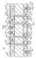
- the construction of one embodiment is explained by referring to Fig. 1 and Fig. 2 .
- Fig. 1 shows a sectional view of a printed wiring board 10
- Fig. 2 shows a state in which an IC chip 90 is mounted on the printed wiring board 10 and the printed wiring board 10 is mounted on a daughter board 94.
- the printed wiring board 10 has a conductor circuit 34 formed on both surfaces of a core substrate 30, and the respective conductor circuits are electrically connected through a plated through hole 36.
- a conductor circuit 58 forming a conductor circuit layer through an interlaminar insulative resin layer 50.
- the conductor circuit 58 is connected to the conductor circuit 34 through via hole 60.
- a conductor circuit 158 is formed through an interlaminar insulative resin layer 150.
- the conductor circuit 158 is connected to the conductor circuit 58 through a via hole 160 formed in an interlaminar insulative resin layer 150.
- a solder resist layer 70 is formed by covering the conductor circuit 158 and the via hole 160, and a connecting pad 75 is formed by forming a nickel plated layer 72 and a gold plated layer 74 on an opening 70 provided in the solder resist layer 71.
- a solder bump 78U On the connecting pad 75 of the top face is formed a solder bump 78U and on the connecting pad 75 of the bottom face is formed a BGA (ball grid array) 78D.
- the solder bump 78U on the top face side of the printed wiring board 10 is connected to an electrode 92 of the IC chip 90 to form an IC mounted printed wiring board, and the IC mounted printed wiring board is connected to a land 96 of a daughter board 94 through the BGA 78D.
- the surface of the solder resist layer corresponding to at least electronic parts mounting region is flattened.
- the solder resist layer and the solder bump are different in thermal expansion coefficient, so that there are produced repeatedly contraction and expansion at the boundary vicinity between the solder bump and the solder resist layer.
- the volume of the solder resist layer in the bump vicinity is small to be easily broken. Therefore, by making flatness of the solder resist layer surface small to some extent, the volume of the solder resist layer where large stress is applied to is increased, bending portion where stress tends to concentrate is lessened, and heat cycle resistance can easily be improved.
- the flattened surface of the solder resist layer is desirably 0.8 to 3.0 ⁇ m in maximum surface roughness. The reason is if the maximum surface roughness is within a range of 0.8 to 3.0 ⁇ m, crack is hardly generated in the solder resist in the vicinity of the conductor pad, and air (void) is hard to enter into the under fill resin. As a result, insulation reliability and connection reliability are improved.
- Wettability of the under fill resin is easily improved by applying the roughening treatment to the surface of the solder resist layer flattened to some extent, so that under fill resin can be filled in a narrow gap portion in the boundary vicinity between the solder resist layer and the solder bump so as to improve connection reliability.
- the roughened surface of the solder resist layer is smaller than the maximum surface roughness of the flattened surface and 0. 2 to 0.5 ⁇ m at an arithmetic mean roughness (Ra).
- the reason is that when the arithmetic mean roughness Ra is made within a range of 0.2 to 0.5 ⁇ m, adhesion to the under fill resin can be increased, and flux residue and cleaning residue are hardly remained on the solder resist surface. As a result, insulation reliability and connection reliability are easily improved.
- two connecting pads positioned at the center are formed in the form of a land right above the viahole 160, two connecting pads adjacent thereto are formed in the form of pads adjacent to the land of the viahole 160, and further two connecting pads positioned at both ends are formed in the form of a pad consisting of a part of a wiring pattern of the conductor circuit 158.
- connecting pads 75 of the bottom face two connecting pads positioned at both ends are formed in the form of a land right above the viahole 160, and four connecting pads positioned at the center are formed in the form of a pad adjacent to a land of the viahole 160.
- the viahole 160 as a connecting pad formed by the solder bump 78U is preferably a filled via, and the uneven amount of the filled via surface exposed from the surface of the interlaminar insulative resin layer 150 is, as shown in Figs. 10A to 10B , desirably within a range of -5 ⁇ m to +5 ⁇ m in relation to the surface thickness of the conductor circuit 158.
- the reason why the depressed or protruded amount of the filled via surface is restricted to a mentioned above is due to the fact that when the depressed amount is more than 5 ⁇ m (-5 ⁇ m), the number of contact point defined by the solder ball and the connecting pad consisting of the filled via is reduced, wettability becomes poor in case of forming the solder bump, and entanglement of voids within the bump and missing bump are not controlled, while when the protruded amount of the filled via surface is more than 5 ⁇ m(+ 5 ⁇ m), the thickness of the conductor circuit 158 becomes too large to be adaptable for fine pitched patterning.
- the "electronic parts mounting region” in the embodiment of the invention substantially corresponds to a region (hereinafter, simply called as "connecting pad region") where conductor pads such as filled via and the like for mounting electronic parts are provided.
- Fig. 11A shows a state of aligning all of the outermost peripheral connecting pads along each side of a rectangle among grid-like aligned connecting pads
- Fig. 11B shows a state of not aligning some of the outermost peripheral connecting pads along each side of the rectangle, however, in either case, when the connecting pad region is made rectangle, a rectangle region determined to minimize an area of the region enclosing all connecting pads is called as "connecting pad region”.
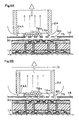
- Figs. 3A to 3C are views explaining the steps for forming the solder bumps on the printed wiring board 10 according to the present invention.
- a flux layer 80 is formed for covering conductor pads formed in the openings 71 provided in the solder resist layer 70 on the top face side of the printed wiring board, i.e. the connecting pads 75 by a printing method (see Fig. 3A ).
- solder ball for example, made by Hitachi Metals or Tamura
- solder ball loader described later on (see Fig. 3B ).
- solder ball is desirable 40 ⁇ m or more and less than 200 ⁇ m in diameter.
- each solder ball does not easily drop on the corresponding connecting pad because it is light in weight, while when the diameter is 200 ⁇ m or more, solder balls are not assembled in a cylinder member, causing the presence of connecting pads with no solder balls mounted thereon.
- the solder ball having a diameter of 80 ⁇ m or less is desirable.
- solder balls 78L of a usual diameter (250 ⁇ m) are adsorbed and placed on the connecting pads 75 on the bottom face side of the printed wiring board with the use of an adsorption head as described in Japanese Patent No. 1975429 , for instance (see Fig. 3C ).
- the pitch of the solder bumps corresponds to a pitch of the connecting pads, and when the pitch of the connecting pads is less than 60 ⁇ m, manufacture of solder balls suitable for the pitch becomes difficult. When the pitch of the connecting pads is more than 200 ⁇ m, it becomes impossible to obtain a printed wiring board adaptable for fine patterning or narrow pitching.
- an IC mounted printed wiring board 10 is formed by mounting the IC chip 90 through the solder bumps 78U by reflowing, and this IC mounted printed wiring board 10 is mounted on the daughter board 94 through BGA 78D.
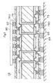
- solder ball loader for mounting the very small solder balls 78s on the corresponding connecting pads of the above-described printed wiring board is explained by referring to Figs. 4A to 4B .
- Fig. 4A is a block diagram showing the structure of the solder ball loader
- Fig. 4B is a view taken from an arrow B of the solder ball loader of Fig 4A .
- the solder ball loader 20 comprises an XY ⁇ suction table 14 for positioning and holding the printed wiring board 10, a vertical moving shaft 12 for moving the XY ⁇ suction table 14 up and down, a ball aligning mask 16 with an opening corresponding to the connecting pad 75 of the printed wiring board, a mounting cylinder (cylinder member) 24 for guiding the solder balls moving on the ball aligning mask 16, a suction box 26 for giving negative pressure to the mounting cylinder 24, a solder ball removing cylinder 61 for recovering excessive solder balls, a suction box 66 for giving negative pressure to the solder ball removing cylinder 61, an adsorbed ball removing and adsorbing device 68 for holding the collected solder balls, a mask clamp 44 for clamping the ball aligning mask 16, an X-axis direction moving shaft 40 for sending the mounting cylinder 24 and the solder ball removing cylinder 61 to the X-axis direction, a moving shaft supporting guide 42 for supporting the X-axis direction moving shaft 40, an alignment camera 46 for taking an
- a plurality of the mounting cylinders 24 and the solder ball removing cylinder 61 are arranged in the Y-axis direction by corresponding to size of the connecting pad regions. Further, the size may correspond to a plurality of the connecting pad areas.
- the Y-axis direction is expedient and may be aligned in the X-axis direction.
- the XY ⁇ suction table 14 functions as positioning, adsorption, maintenance and correction of the solder ball mounted printed wiring board 10.
- the alignment camera 46 detects an alignment mark of the printed wiring board 10 on the XY ⁇ suction table 14 to regulate a position between the printed wiring board 10 and the ball aligning mask 16 based on the detected position.
- the residue detecting sensor 18 detects the residue of the solder balls by an optical method.
- an alignment mark 34M of the printed wiring board 10 is recognized by the alignment camera 46, and the position of the printed wiring board 10 in relation to the ball aligning mask 16 is corrected by the suction table 14. That is, openings 16a of the ball aligning mask 16 are adjusted for corresponding to the connecting pads 75 of the printed wiring board 10 in position, respectively.
- solder balls are mounted to a printed wiring board of worksheet size for constructing a plurality of printed wiring boards, and after forming solder bumps, the worksheet size board is cut into respective multilayer printed wiring boards.
- solder balls 78s are supplied from a solder ball supplying device 22 to the side of the mounting cylinder 24.
- solder ball any commercial item (a product of Hitachi Metals, for example) may be used or, solder balls may be manufactured according to the manufacturing device and method described in Japanese unexamined patent application No. 2001-226705 .
- solder balls are placed on a metal plate (e.g. nickel plate of 25 ⁇ m thick) having a square slit (opening) of which length and breadth are smaller than a designated diameter of the solder ball by 1 ⁇ m, and the solder balls are rolled thereon and dropped from the slit. Then, small balls having smaller diameters than designated are removed. Thereafter, the solder balls remained on the metal plate are classified by a metal plate having a square slit of which length and breadth are larger than the desired diameter of the solder ball by 1 ⁇ m, and solder balls dropped from the slit are collected so as to obtain the solder balls having a substantially equal diameter to the desired diameter.
- a metal plate e.g. nickel plate of 25 ⁇ m thick
- solder balls are rolled thereon and dropped from the slit.
- small balls having smaller diameters than designated are removed.
- solder balls remained on the metal plate are classified by a metal plate having a square slit of which length and bread
- solder balls 78s are assembled on the ball aligning mask 16 right under the opening 24A of the mounting cylinder 24 by adsorbing air from the suction portion 24B at a running speed of 5 m/sec to 35 m/sec in a gap between the mounting cylinder and the printed wiring board.
- the mounting cylinders 24 aligned along the Y-axis of the printed wiring board 10 are sent to the horizontal direction along the X-axis by means of the X-axis direction moving shaft 40.
- the solder balls 78s assembled on the ball aligning mask 16 are moved with the movement of the mounting cylinder 24, dropped to the corresponding connecting pads 75 of the printed wiring board 10 through the openings 16a of the ball aligning mask 16 and loaded.
- the solder balls 78s are successively aligned on the whole connecting pads on the side of the printed wiring board 10.
- the excessive solder balls 78s are guided to a place having no opening 16a on the ball aligning mask 16, then adsorbed and removed by the solder ball removing cylinder 61.
- the solder balls 78s are assembled by positioning the mounting cylinder 24 on the upper part of the ball aligning mask 16 and adsorbing air from the suction portion 24B on the top of the mounting cylinder 24, the assembled solder balls 78s are moved on the ball aligning mask 16 by moving the mounting cylinder 24 in the horizontal direction, and the solder balls 78s can be dropped to the respective connecting pads 75 of the printed wiring board 10 through the respective openings 16a of the ball aligning mask 16.
- solder balls 78s can certainly be mounted on the whole of the connecting pads 75 of the printed wiring board 10. Further, since the solder balls 78s can be moved with no contact, the solder balls can be mounted on the connecting pads 75 without damage, which is different from a printing method with the use of a conventional squeeze, and the solder bumps 78U can be equalized in height.
- the fine solder balls could certainly be placed on the connecting pads, even in the printed wiring board having such a narrow pitch alignment that the connecting pad pitch is 60 to 200 ⁇ m and the solder resist opening diameter is 40 to 150 ⁇ m, in the whole of bumps, stable bumps having substantially uniform heights can be formed.
- solder balls are guided by suction force so as to prevent aggregation and adhesion of solder balls. Further, adjusting number of the mounting cylinder 24 so as to be applied to many forms and small production enables the applicability to various sizes of the works (multilayer printed wiring board of work sheet size).
- the mounting cylinders 24 are aligned in the Y direction by corresponding to width of the work (printed wiring board of work sheet size), so that the solder balls can positively be mounted on the whole of connecting pads 75 of the printed wiring boards by simply sending a plurality of mounting cylinders 24 to the vertical direction (X direction) in relation to the row direction.
- solder balls 78s remained on the ball aligning mask 16 can be collected by the solder ball removing cylinder 61, so that there are no problem such that excessive solder ball are remained to cause any trouble and the like.
- solder balls mounted on the connecting pads of the wiring substrate become solder bumps having predetermined height by means of a reflow treatment, IC chips are mounted on the substrate through such solder bumps, and the printed wiring board according to the present invention is manufactured.
- a double sided copper-clad laminate e.g. "MCL-E-67” made by Hitachi Chemical
- a through-hole conductor and a conductor circuit by a known method.
- insulating layers and conductor circuit layers are alternately laminated by a known method (e.g.
- connecting pads are formed by a method similar to that described in Japanese unexamined patent application No. 2000-357762 .
- the pattern (opening diameter, pitch, arrangement, etc.) of a plated resist is changed.
- Formation of a solder resist layer is that screen printing is carried out under the following printing condition with the use of a commercial solder resist to form a solder resist layer having a thickness of 15 to 25 ⁇ m (on the connecting pad) for covering the connecting pad.
- Solder resist ink "RPZ-1" made by Hitachi Kogyo Ink viscosity : 45 ⁇ 15 Pa ⁇ s Screen : polyester fiber (130 to 300 mesh) Squeeze speed : 100 to 200 mm/sec
- thickness of the solder resist layer is 25 ⁇ m.
- a photo mask having a pattern (mask pattern) of opening of solder resist thereon is exposed to ultraviolet ray of 100 to 1000 mJ under the state of adhering to the solder resist layer, and developed with a sodium carbonate solution (Na 2 CO 3 ) of 10 g/L, thereby forming an opening of 120 ⁇ m in diameter on the connecting pad.
- a sodium carbonate solution Na 2 CO 3
- solder balls are loaded on the suction table of a solder ball loader, alignment marks of the printed wiring board and the ball aligning mask are recognized by using a CCD camera, and alignment of the printed wiring board and the ball aligning mask is carried out.
- a metal mask made of Ni is used having openings of 175 ⁇ m in diameter at the position corresponding to the connecting pads of the printed wiring board.
- an opening diameter formed in the ball aligning mask is preferably 1.1 to 1.5 times the ball diameter used, and a thickness of the ball aligning mask is preferably 1/2 to 3/4 of the diameter of the solder ball used.
- Sn/Pb is used for the solder ball
- Pb free solder consisting of at least one metal and Sn selected from the group of Ag, Co, In, Bi, Zn and the like.
- air is adsorbed from the top of the mounting cylinder, and the gap running speed between the mounting cylinder and the printed wiring board is regulated to 5 to 35 m/sec for assembling the solder balls within the mounting cylinder.
- the mounting cylinder is moved at 10 to 40 mm/sec of the moving speed to roll the solder balls, and the solder balls are dropped from the respective openings of the ball aligning mask and mounted on the corresponding connection pads.
- solder ball aligning mask and the printed wiring board are separately taken out of the solder ball loader, and finally, the printed wiring board is put in the reflowing apparatus set at 230°C to form a solder bump.
- a height of the solder bump protruded from the solder resist surface is measured by a laser microscope ("VX-8500” made by KEYENCE or "WYKO NT-2000” made by Veeco).
- measurement points are four corners and a center of a rectangle, i.e. four solder bumps located at the four corners of a rectangle defined by the connecting pad group and a solder bump substantially positioned at the center of the rectangle are measured at this time, and five solder balls in total are measured.
- the minimum value of the solder bump height is 66 ⁇ m and the maximum value thereof is 70 ⁇ m.
- an IC chip is mounted through the solder bumps, and an IC chip mounted printed wiring board is manufactured by filling a commercial under fill resin between the IC chip and the solder resist.
- the mask pattern of a photo mask in case of forming a solder resist opening is changed to change the solder resist opening diameter to 90 ⁇ m
- the printing condition (mesh of screen and printing speed) of the solder resist is regulated
- film thickness of the solder resist is made 10 ⁇ m
- the solder ball having a diameter of 90 ⁇ m is mounted with the use of the ball aligning mask having an opening diameter of 110 ⁇ m
- a printed wiring board is manufactured in the same manner as in Example 1.
- the minimum value of the solder bump height becomes 46 ⁇ m and the maximum value thereof becomes 49 ⁇ m.
- the mask pattern of the photo mask in case of forming a solder resist opening is set to change the solder resist opening diameter to 60 ⁇ m
- the printing condition (mesh of screen and printing speed) of the solder resist is regulated
- film thickness of the solder resist is made 10 ⁇ m
- the solder ball having a diameter of 50 ⁇ m is mounted with the use of the ball aligning mask having an opening diameter of 60 ⁇ m
- a printed wiring board is manufactured in the same manner as in Example 1.
- the minimum value of the solder bump height becomes 31 ⁇ m and the maximum value thereof becomes 34 ⁇ m.
- solder ball having a diameter of 160 ⁇ m is mounted with the use of the ball aligning mask having an opening diameter of 190 ⁇ m
- a printed wiring board is manufactured in the same manner as in Example 1.
- the minimum value of the solder bump height becomes 84 ⁇ m and the maximum value thereof becomes 87 ⁇ m.
- solder ball having a diameter of 215 ⁇ m is mounted with the use of the ball aligning mask having an opening diameter of 260 ⁇ m, a printed wiring board is manufactured in the same manner as in Example 2.
- the minimum value of the solder bump height becomes 100 ⁇ m and the maximum value thereof becomes 180 ⁇ m.
- solder ball having a diameter of 170 ⁇ m is mounted with the use of the ball aligning mask having an opening diameter of 200 ⁇ m, a printed wiring board is manufactured in the same manner as in Example 8. As a result, the minimum value of the solder bump height becomes 75 ⁇ m and the maximum value thereof becomes 160 ⁇ m.
- solder ball having a diameter of 120 ⁇ m is mounted with the use of the ball aligning mask having an opening diameter of 150 ⁇ m, a printed wiring board is manufactured in the same manner as in Example 12. As a result, the minimum value of the solder bump height becomes 75 ⁇ m and the maximum value thereof becomes 90 ⁇ m.
- Example 1 Examples Diameter of Connecting Pad ( ⁇ m) Pitch of Connecting Pad ( ⁇ m) Thickness of Solder Resist Layer ( ⁇ m) Opening Diameter of Solder Resist Layer ( ⁇ m) Diameter of Solder Ball ( ⁇ m) Opening Diameter of Mask ( ⁇ m) Height of Bamp (minimum) ( ⁇ m) Height of Bamp(Maximum) ( ⁇ m) Height of Bamp/ Opening Diameter of SR Heat Cycle Test 500 cycles 1000 cycles
- Example 6 120 150 15 90 95 115 45 49 0.50 ⁇ ⁇
- Example 7 120 150 20 90 100 120 47 49 0.52 ⁇ ⁇
- Example 8 120 150 25 90 105 130 47 49 0.
- Examples 37 to 45 printed wiring boards made by applying the following flattening treatment to the solder resist layer surface are manufactured, and these are denoted as Examples 37 to 45.
- a connecting pad region for mounting IC chip (region area: 1200 mm 2 , connecting pad number: 30000) is measured by means of a surface roughness measuring instrument (e.g. "SURFCOM 480A” made by Tokyo Seimitsu or “WYKO N-2500” by Veeco) to examine uneven amount (see Fig, 8 ) due to the presence or absence of conductor pads. As a result, the uneven amount of the solder resist layer surface becomes 7.2 to 9.8 ⁇ m.
- a surface roughness measuring instrument e.g. "SURFCOM 480A” made by Tokyo Seimitsu or "WYKO N-2500” by Veeco
- PET polyethylene terephthalate
- maximum uneven amount and “minimum uneven amount” mentioned herein mean, as shown in Fig. 8 , maximum value and minimum value of differences X1, X2, X3, X4, X5 ⁇ ⁇ ⁇ ⁇ between height of the solder resist layer on the conductor pad or conductor circuit and that of the solder resist layer of adjacent conductor pad non-forming part or conductor circuit non-forming part in the electronic part mounting region.
- An uneven amount of the surface before flattening the solder resist layer obtained in this example is comparatively as large as about 6.6 to 10.2 ⁇ m, but the amount of the flattened surface is as small as about 0.7 to 3.0 ⁇ m.
- An uneven amount of the surface before flattening the solder resist layer obtained in this example is comparatively as large as about 8.4 to 9.3 ⁇ m, but that of the flattened surface is as small as about 0.8 to 3.1 ⁇ m.
- An uneven amount of the surface before flattening the solder resist layer obtained in this example is large such as about 8.2 to 9.6 ⁇ m, but that of the flattened surface is small such as about 0.7 to 3.2 ⁇ m.
- An uneven amount of the surface before flattening the solder resist layer obtained in this example is comparatively as large as about 9.9 to 10.2 ⁇ m, but that of the flattened surface is as small as about 0.8 to 3.3 ⁇ m.
- An uneven amount of the surface before flattening the solder resist layer obtained in this example is comparatively large such as about 8.3 to 10.3 ⁇ m, but that of the flattened surface is small such as about 0.7 to 3.0 ⁇ m.
- An uneven amount of the surface before flattening the solder resist layer obtained in this example is comparatively large such as about 9.1 to 9.8 ⁇ m. but that of the flattened surface is small such as about 0.5 to 3.1 ⁇ m.
- An uneven amount of the surface before flattening the solder resist layer obtained in this example is comparatively large such as about 8.1 to 10.2 ⁇ m, but that of the flattened surface is small such as about 0.8 to 3.0 ⁇ m.
- An uneven amount of the surface before flattening the solder resist layer obtained in this example is comparatively large such as about 9.6 to 10.3 ⁇ m, but that of the flattened surface is small such as about 0.7 to 3.0 ⁇ m.
- Example 40 (14) 0.7 3.2 ⁇ ( ⁇ ) ⁇ (X) Example 41 (19) 0.8 3.3 ⁇ ( ⁇ ) ⁇ (X) Example 42 (23) 0.7 3.0 ⁇ ( ⁇ ) ⁇ (X) Example 43 (26) 0.5 3.1 ⁇ ( ⁇ ) ⁇ (X) Example 44 (31) 0.8 3.0 ⁇ ( ⁇ ) ⁇ (X) Example 45 (35) 0.7 3.0 ⁇ ( ⁇ ) ⁇ (X)
- Roughening solution potassium permanganate solution Concentration: 60 to 80 g/l Temperature: 60 to 80°C Immersion time: 1 to 5 minutes
- surface roughness of the solder resist surface is randomly measured at 10 spots by surface roughness measuring instrument (for example, "SURFCOM 480A” made by Tokyo Seimitsu or "WYKO N-2500” made by Veeco).
- surface roughness measuring instrument for example, "SURFCOM 480A” made by Tokyo Seimitsu or "WYKO N-2500” made by Veeco.
- surface roughness (Ra) mentioned here means “arithmetic mean roughness (Ra)” prescribed by JIS B0601, but Ra within a range of the above measuring result is mentioned that the smallest Ra is Ra(min) and the largest one is Ra(max) in measured 10 spots.
- surface roughness is measured at random 10 spots in the solder resist layer surface corresponding to the conductor circuit (pad) forming region and the solder resist layer surface corresponding to the conductor circuit non-forming region, but not measured in the boundary vicinity of the conductor circuit forming region and the conductor circuit non-forming region.
- Roughening solution potassium permanganate solution Concentration: 60 to 80 g/l Temperature: 60 to 80°C Immersion time: 1 to 5 minutes
- Example 39 Except that roughening treatment is further applied to the solder resist layer surface with the following condition after flattening treatment, a printed wiring board is manufactured in the same manner as in Example 39.
- Roughening solution potassium permanganate solution Concentration: 60 to 80 g/l Temperature: 60 to 80°C Immersion time: 1 to 5 minutes
- Example 40 Except that roughening treatment is further applied to the solder resist layer surface with the following condition after flattening treatment, a printed wiring board is manufactured in the same manner as in Example 40.
- Roughening solution potassium permanganate solution Concentration: 60 to 80 g/l Temperature: 60 to 80°C Immersion time: 1 to 5 minutes
- Roughening solution potassium permanganate solution Concentration: 60 to 80 g/l Temperature: 60 to 80°C Immersion time: 1 to 5 minutes
- Roughening solution potassium permanganate solution Concentration: 60 to 80 g/l Temperature: 60 to 80°C Immersion time: 1 to 5 minutes
- Roughening solution potassium permanganate solution Concentration: 60 to 80 g/l Temperature: 60 to 80°C Immersion time: 1 to 5 minutes
- Example 44 Except that roughening treatment is further applied to the solder resist layer surface with the following condition after flattening treatment, a printed wiring board is manufactured in the same manner as in Example 44.
- Roughening solution potassium permanganate solution Concentration: 60 to 80 g/l Temperature: 60 to 80°C Immersion time: 1 to 5 minutes
- Example 45 Except that roughening treatment is further applied to the solder resist layer surface with the following condition after flattening treatment, a printed wiring board is manufactured in the same manner as in Example 45.
- Roughening solution potassium permanganate solution Concentration: 60 to 80 g/l Temperature: 60 to 80°C Immersion time: 1 to 5 minutes
- connection reliability is improved.
- unevenness of the solder resist layer surface due to the presence or absence of the connecting pad positioned beneath the solder resist is flattened, and when roughness of the flattened surface is 0.8 to 3 ⁇ m of maximum surface roughness (uneven amount), connection reliability is improved.
- connection reliability is further improved. It is assumed that adhesion between the under fill resin and the solder resist layer surface is easily improved, or flux and flux cleaning solvent are hard to remain within a recess of the surface.
- the printed wiring boards manufactured according to Examples 1 to 54 and Comparative Examples 1 to 24 are left in atmosphere of temperature: 85°C and humidity: 85% by applying voltage of 3.3V between adjacent and not shorted solder bumps for 50 hours. Thereafter, insulation resistance between the voltage-applied solder bumps is measured.
- insulation performance is "good (O) "and when insulation resistance is less than 10 7 ⁇ , insulation performance is "no good (x)" for evaluation.
- voids within solder bumps are observed by using an X-ray television system ("SMX-100" made by Shimazu Corporation) and number of voids is measured. 100 solder bumps are randomly selected, but no void is observed.
- SMX-100 X-ray television system
- Examples 1 to 54 As to the printed wiring boards manufactured according to Examples 1 to 54, except that number of connection pad is changed from 2000 (connecting pad region: about 150 mm 2 ) to 30000 (connecting pad region: 1200 mm 2 ), an IC mounted printed wiring board is manufactured in the same manner as in Examples 1 to 54, each of these examples is conducted to heat cycle test, HAST test and observation of voids in solder bump in the same manner as in Examples 1 to 54, and the same results as Examples 1 to 54 can be obtained.
- the printed wiring board of the invention easily improves connection reliability and insulation reliability, even narrow pitch structure such as 200 ⁇ m or less pitch of solder bump, by making a ratio (H/D) of height H from the solder resist layer surface to opening diameter D of the opening 0.55 to 1.0.
Abstract
Description
- The present invention relates to a printed wiring board for mounting electronic parts such as capacitors, IC and the like on the outer layer, more particularly, a printed wiring board adaptable to narrow pitching of solder bump for mounting electronic parts.
- Recent years, high performance is remarkable in electronics represented by portable telephones and communication terminals. And, for these electronics is used a printed wiring board having IC chips mounted thereon. As a form of mounting an IC chip on a printed wiring board, a flip chip type of directly mounting an IC chip on the surface of a printed wiring board is widely employed. As such a printed wiring board, there has been known the one comprising a core substrate, a build-up layer formed on the core substrate and connecting pads for mounting an IC chip through a solder bump on the surface of the build-up layer.
- Here, a printed wiring board is made of epoxy resin, BT (bismaleimide triazine) resin phenol resin and the like formed with reinforcement such as glass fiber or the like. The thermal expansion coefficient of these core substrates is about 12-20 ppm/°C (30 - 200°C) and about 4 times larger than that (about 3.5 ppm/°C) of silicon of the IC chip.
- Therefore, the flip-chip type has, in case of repeating temperature change with heat generation, the possibility of destroying the solder bump due to differences in thermal expansion and heat contraction between the IC chip and the core substrate. For solving such problem, there is proposed a method of interposing an interposer having a thermal expansion coefficient between the printed wiring board and the IC (refer to
Japanese unexamined patent application No. 59-996 - However, the method of interposing an interposer between the IC and the printed wiring board cannot meet needs of downsizing of electronic parts. Further, addition of an excessive part such as the interposer makes the cost high.
- Accordingly, an object of the present invention is to solve the above problem of prior art by providing a printed wiring board having excellent connection reliability and insulation reliability which can make downsizing and low cost possible even with narrow pitch structure having conductor pads (connecting pads) provided for mounting solder bumps thereon with a pitch of 200 µm or less.
- The inventors have, as a result of earnest study for realizing the above object, completed the invention having the following essentials and construction based on such knowledge that connection reliability and insulation reliability between the solder bump and electronic parts such as IC chips and the like are improved by limiting the ratio of height of the solder bump provided on the connecting pad exposed from an opening provided in a solder resist layer to diameter of the opening to a predetermined range so as to contribute to the downsizing and low cost.
- That is, the present invention provides
- (1) a printed wiring board comprising a wiring substrate provided with at least one conductor circuit, a solder resist layer formed on the surface of the wiring substrate, covering the at least one conductor circuit, conductor pads formed on a part of the at least one conductor circuit exposed from respective openings provided in the solder resist layer for mounting electronic parts, and solder bumps formed on the respective conductor pads, wherein the conductor pads are arranged with a pitch of 200 µm or less and the ratio (H/D) of a height H of the solder bump from the surface of the solder resist layer to an opening diameter D of the opening is 0.55 to 1.0.
Further, the present invention provides - (2) a printed wiring board comprising a wiring substrate provided with at least one conductor circuit, a solder resist layer formed on the surface of the wiring substrate, covering the at least one conductor circuit, conductor pads formed on a part of the at least one conductor circuit exposed from the respective openings provided in the solder resist for mounting electronic parts, solder bumps formed on the respective conductor pads, and an under fill material or resin for sealing a gap or space defined between electronic parts mounted through the solder bumps and the solder resist layer, wherein the conductor pads are arranged with a pitch of 200 µm or less and the ratio (H/D) of a height H of the solder bump from the surface of the solder resist layer to an opening diameter D of the opening is 0.55 to 1.0.
- In the present invention, the surface of the solder resist layer can be flattened at least in an electronic part mounting region, and it is desirable that maximum surface roughness (uneven amount) of the flattened surface (1st uneven face) is made 0.8 to 3.0 µ m.
- Further, in the present invention, the surface of the flattened solder resist layer can be further roughened, and it is desirable that surface roughness of the surface (2nd uneven face) of the roughened solder resist layer is smaller than the maximum surface roughness of the flattened surface and 0.2 to 0.5 µm at an arithmetic mean roughness (Ra).
- Further, in the present invention, it is desirable that the conductor pad defined as a part of the conductor circuit exposed from the opening provided in the solder resist layer is formed in the form of a filled via which is defined by a plated conductor completely filled within an opening provided in an interlaminar insulative resin layer positioned at the outermost layer, and an uneven amount of the filled via surface exposed from the interlaminar insulative resin layer surface is -5 µm to +5 µm in relation to the thickness of the conductor circuit formed on the interlaminar insulative resin layer.
- Further, in the present invention, "conductor pad" is defined as a part of the conductor circuit exposed from the opening provided in the solder resist layer. The conductor circuit can be, for instance, formed in the form (connecting pad) of utilizing a part of the conductor circuit, the form of a viahole (including the filled via in which plated conductor is completely filled within the opening provided in the resin insulating layer) or the form consisting of the viahole and the conductor circuit, so that in a broad sense, it indicates a part of the conductor circuit including the connecting pads and the viaholes.
- Further, in the present invention, "opening diameter (D)" of the opening provided in the solder resist layer means a "diameter" of the opening when the opening side wall is not tapered, and means a diameter (of the opening upper part) of the opening exposed on the solder resist layer surface when the opening side wall is tapered.
- Further, in the present invention, "maximum surface roughness" means, as schematically shown in
Fig. 8 , in the electronic part mounting region, the maximum value in differences X1, X2, X3, X4, X5, ... between the height of the solder resist layer on the conductor pad or the conductor circuit and that of the solder resist layer on an adjacent conductor pad non-forming portion or a conductor circuit non-forming portion. - Further, "arithmetic mean roughness" means arithmetic mean roughness (Ra) prescribed in JIS B0601.
- According to the present invention, a height of the solder bump can be made comparatively large by making a ratio (H/D) of the height H of the solder bump from the solder resist layer surface to the opening diameter D of the opening 0.55 or more, thereby easily deforming the solder bump itself and enlarging volume (amount) of the solder. As a result, stress which can be absorbed by the solder is increased to improve connection reliability. On the other hand, the solder fused between the adjacent solder bumps is hard to move by making a ratio (H/D) of the height H of the solder bump from the solder resist layer surface to the opening diameter D of the opening 1.0 or less, thereby hardly moving the solder molten between adjacent solder bumps to control irregular solder bump height and to prevent short-circuit of adjacent solder bumps. As a result, connection reliability and insulation reliability are improved.
- Further, the flattened surface (1st uneven face) in at least the electronic part mounting region of the solder resist layer surface can decrease generation of void in the under fill material filled between the solder resist layer surface and the mounted electronic parts by making the maximum surface roughness (uneven amount) 0.8 to 3.0 µm. As a result, connection reliability is improved.
- Further, when surface roughness of the surface (2nd uneven face) of the roughened solder resist layer is made smaller than an uneven amount of the flattened surface and about 0.2 to 0.5µ m at an arithmetic mean roughness Ra, adhesion between the solder resist layer surface and the under fill material can be improved, and residual material such as flux, cleaning solution and the like on the solder resist layer surface can be lessened. As a result, connection reliability and insulation reliability are improved.
- Further, the conductor pad is formed into a filled via and the uneven amount of the filled via surface exposed from the outermost interlaminar insulative resin layer surface is made from -5 µm to +5 µm in relation to the thickness of a conductor circuit formed on the interlaminar insulative resin layer, thereby increasing contact points between the filled via and the solder ball so as to improve wettability in case of forming a solder bump, to lessen catching up or involvement of void within the solder bump and missing bump and to obtain fine adaptability.
- Further, without requiring any interposer, the board can be thinned and the cost can be lowered at the same time.
-
-
Fig. 1 is a sectional view of the printed wiring board according to the present invention. -
Fig. 2 is a sectional view showing a state of mounting an IC chip on the printed wiring board shown inFig. 1 and placing on a daughter board. -
Figs. 3A to 3C are views explaining steps of forming solder bumps on the printed wiring board. -
Figs 4A to 4B are schematic views showing structure of an apparatus for mounting the solder balls on the wiring board. -
Fig. 5A is a schematic view explaining positioning of the printed wiring board, andFig 5B is a schematic view explaining supply of solder balls to mounting cylinders. -
Fig. 6A is a schematic view explaining assembly of solder balls by mounting cylinders, andFig. 6B is a schematic view explaining assembly and guidance of solder balls by the mounting cylinders. -
Fig. 7A is a schematic view explaining dropping solder balls to connecting pads, andFig. 7B is a schematic view explaining removal of solder balls by adsorbed-ball removing cylinder. -
Fig. 8 is a schematic view explaining maximum surface roughness of the solder resist layer surface. -
Fig. 9 is a schematic view explaining relation between bump height (H) and solder resist layer opening diameter (D) according to the present invention. -
Figs. 10A to 10B are schematic views explaining unevenness of the filled via surface as a connecting pad. -
Figs. 11A to 11B are schematic views explaining connecting pad region. - One embodiment of the printed wiring board according to the present invention will be described hereinafter. In the printed wiring board, as shown in
Fig. 9 , at least one opening is provided in a solder resist layer (SR layer) formed on the outermost layer of a wiring board, a part of the conductor circuit exposed from the at least one opening is formed as connecting pads, the connecting pads are arranged with a pitch of 200 µm or less, and solder bumps are formed on the respective connecting pads, a ratio (H/D) of a height H from the solder resist layer surface of the solder bump formed on the connecting pad to the opening diameter D is within a range of 0.55 to 1.0. - In the embodiment of the present invention, for forming the respective solder bumps in the corresponding openings provided in the solder resist layer, it is desirable to use a novel method and a device for dropping solder balls having very fine particle diameter on the connecting pads through the corresponding openings of a ball aligning mask as described below, without employing a printing method with the use of a conventional mask.
- First, a novel solder ball mounting method and a device thereof are used for manufacturing. As to the printed wiring board of the present invention, the construction of one embodiment is explained by referring to
Fig. 1 andFig. 2 . -
Fig. 1 shows a sectional view of a printedwiring board 10, andFig. 2 shows a state in which anIC chip 90 is mounted on the printedwiring board 10 and the printedwiring board 10 is mounted on adaughter board 94. As shown inFig. 1 , the printedwiring board 10 has aconductor circuit 34 formed on both surfaces of acore substrate 30, and the respective conductor circuits are electrically connected through a plated throughhole 36. - Further, on the
conductor circuit 34 of thecore substrate 30 is formed aconductor circuit 58 forming a conductor circuit layer through an interlaminarinsulative resin layer 50. Theconductor circuit 58 is connected to theconductor circuit 34 through viahole 60. On theconductor circuit 58 is formed aconductor circuit 158 through an interlaminarinsulative resin layer 150. Theconductor circuit 158 is connected to theconductor circuit 58 through a viahole 160 formed in an interlaminarinsulative resin layer 150. - A solder resist
layer 70 is formed by covering theconductor circuit 158 and the viahole 160, and a connectingpad 75 is formed by forming a nickel platedlayer 72 and a gold platedlayer 74 on anopening 70 provided in the solder resistlayer 71. On the connectingpad 75 of the top face is formed asolder bump 78U and on the connectingpad 75 of the bottom face is formed a BGA (ball grid array) 78D. - As shown in
Fig. 2 , thesolder bump 78U on the top face side of the printedwiring board 10 is connected to anelectrode 92 of theIC chip 90 to form an IC mounted printed wiring board, and the IC mounted printed wiring board is connected to aland 96 of adaughter board 94 through theBGA 78D. - Further, it is desirable that the surface of the solder resist layer corresponding to at least electronic parts mounting region is flattened. The solder resist layer and the solder bump are different in thermal expansion coefficient, so that there are produced repeatedly contraction and expansion at the boundary vicinity between the solder bump and the solder resist layer. And, when large unevenness is existent on the solder resist layer surface, i.e. less flatness, the volume of the solder resist layer in the bump vicinity is small to be easily broken. Therefore, by making flatness of the solder resist layer surface small to some extent, the volume of the solder resist layer where large stress is applied to is increased, bending portion where stress tends to concentrate is lessened, and heat cycle resistance can easily be improved.
- The flattened surface of the solder resist layer is desirably 0.8 to 3.0 µm in maximum surface roughness. The reason is if the maximum surface roughness is within a range of 0.8 to 3.0 µm, crack is hardly generated in the solder resist in the vicinity of the conductor pad, and air (void) is hard to enter into the under fill resin. As a result, insulation reliability and connection reliability are improved.
- Further, in the embodiment of the present invention, it is desirable to further apply a roughening treatment to the flattened surface of the solder resist layer.
- Wettability of the under fill resin is easily improved by applying the roughening treatment to the surface of the solder resist layer flattened to some extent, so that under fill resin can be filled in a narrow gap portion in the boundary vicinity between the solder resist layer and the solder bump so as to improve connection reliability.
- It is desirable that the roughened surface of the solder resist layer is smaller than the maximum surface roughness of the flattened surface and 0. 2 to 0.5 µm at an arithmetic mean roughness (Ra).
- The reason is that when the arithmetic mean roughness Ra is made within a range of 0.2 to 0.5 µm, adhesion to the under fill resin can be increased, and flux residue and cleaning residue are hardly remained on the solder resist surface. As a result, insulation reliability and connection reliability are easily improved.
- In the embodiment of the present invention, as understood from
Fig. 1 andFig. 2 , among the connectingpads 75 provided on the surface of the substrate as conductor pads for mounting electronic parts, two connecting pads positioned at the center are formed in the form of a land right above theviahole 160, two connecting pads adjacent thereto are formed in the form of pads adjacent to the land of theviahole 160, and further two connecting pads positioned at both ends are formed in the form of a pad consisting of a part of a wiring pattern of theconductor circuit 158. - Further, among the connecting
pads 75 of the bottom face, two connecting pads positioned at both ends are formed in the form of a land right above theviahole 160, and four connecting pads positioned at the center are formed in the form of a pad adjacent to a land of theviahole 160. - The
viahole 160 as a connecting pad formed by thesolder bump 78U is preferably a filled via, and the uneven amount of the filled via surface exposed from the surface of the interlaminarinsulative resin layer 150 is, as shown inFigs. 10A to 10B , desirably within a range of -5 µm to +5 µm in relation to the surface thickness of theconductor circuit 158. The reason why the depressed or protruded amount of the filled via surface is restricted to a mentioned above is due to the fact that when the depressed amount is more than 5 µm (-5 µm), the number of contact point defined by the solder ball and the connecting pad consisting of the filled via is reduced, wettability becomes poor in case of forming the solder bump, and entanglement of voids within the bump and missing bump are not controlled, while when the protruded amount of the filled via surface is more than 5 µm(+ 5 µm), the thickness of theconductor circuit 158 becomes too large to be adaptable for fine pitched patterning. - Further, the "electronic parts mounting region" in the embodiment of the invention substantially corresponds to a region (hereinafter, simply called as "connecting pad region") where conductor pads such as filled via and the like for mounting electronic parts are provided.
- For example,
Fig. 11A shows a state of aligning all of the outermost peripheral connecting pads along each side of a rectangle among grid-like aligned connecting pads, andFig. 11B shows a state of not aligning some of the outermost peripheral connecting pads along each side of the rectangle, however, in either case, when the connecting pad region is made rectangle, a rectangle region determined to minimize an area of the region enclosing all connecting pads is called as "connecting pad region". -
Figs. 3A to 3C are views explaining the steps for forming the solder bumps on the printedwiring board 10 according to the present invention. - First, a
flux layer 80 is formed for covering conductor pads formed in theopenings 71 provided in the solder resistlayer 70 on the top face side of the printed wiring board, i.e. the connectingpads 75 by a printing method (seeFig. 3A ). - Next, on the connecting
pads 75 on the top face side of the printed wiring board are mounted verysmall solder balls 78s (for example, made by Hitachi Metals or Tamura) with the use of a solder ball loader described later on (seeFig. 3B ). Such solder ball is desirable 40 µm or more and less than 200 µm in diameter. When the diameter is less than 40 µm, each solder ball does not easily drop on the corresponding connecting pad because it is light in weight, while when the diameter is 200 µm or more, solder balls are not assembled in a cylinder member, causing the presence of connecting pads with no solder balls mounted thereon. In order to match for the fine patterning, the solder ball having a diameter of 80 µm or less is desirable. - Thereafter, solder balls 78L of a usual diameter (250 µm) are adsorbed and placed on the connecting
pads 75 on the bottom face side of the printed wiring board with the use of an adsorption head as described inJapanese Patent No. 1975429 Fig. 3C ). - Next, by heating in a reflow furnace to form, 500 pieces to 30,000 pieces of the solder bumps 78U are formed with a pitch of 60 to 200 µm on the top face side of the printed
wiring board 10 as shown inFig. 1 , and 250 pieces ofBGA 78D are formed with a pitch of 2 mm on the bottom face side thereof, for instance. - The pitch of the solder bumps corresponds to a pitch of the connecting pads, and when the pitch of the connecting pads is less than 60 µm, manufacture of solder balls suitable for the pitch becomes difficult. When the pitch of the connecting pads is more than 200 µm, it becomes impossible to obtain a printed wiring board adaptable for fine patterning or narrow pitching.
- Further, as shown in
Fig. 2 , an IC mounted printedwiring board 10 is formed by mounting theIC chip 90 through the solder bumps 78U by reflowing, and this IC mounted printedwiring board 10 is mounted on thedaughter board 94 throughBGA 78D. - Next, the solder ball loader for mounting the very
small solder balls 78s on the corresponding connecting pads of the above-described printed wiring board is explained by referring toFigs. 4A to 4B . -
Fig. 4A is a block diagram showing the structure of the solder ball loader, andFig. 4B is a view taken from an arrow B of the solder ball loader ofFig 4A . - The
solder ball loader 20 comprises an XYθ suction table 14 for positioning and holding the printedwiring board 10, a vertical movingshaft 12 for moving the XYθ suction table 14 up and down, aball aligning mask 16 with an opening corresponding to the connectingpad 75 of the printed wiring board, a mounting cylinder (cylinder member) 24 for guiding the solder balls moving on theball aligning mask 16, asuction box 26 for giving negative pressure to the mountingcylinder 24, a solderball removing cylinder 61 for recovering excessive solder balls, asuction box 66 for giving negative pressure to the solderball removing cylinder 61, an adsorbed ball removing and adsorbingdevice 68 for holding the collected solder balls, amask clamp 44 for clamping theball aligning mask 16, an X-axisdirection moving shaft 40 for sending the mountingcylinder 24 and the solderball removing cylinder 61 to the X-axis direction, a moving shaft supporting guide 42 for supporting the X-axisdirection moving shaft 40, analignment camera 46 for taking an image of the multilayer printedwiring board 10, aresidue detecting sensor 18 for detecting residual amount of the solder balls under the mountingcylinder 24 and asolder ball supplier 22 for supplying solder balls to the side of the mountingcylinder 24 based on the residue detected by theresidue detecting sensor 18. - A plurality of the mounting
cylinders 24 and the solderball removing cylinder 61 are arranged in the Y-axis direction by corresponding to size of the connecting pad regions. Further, the size may correspond to a plurality of the connecting pad areas. Here, the Y-axis direction is expedient and may be aligned in the X-axis direction. The XYθ suction table 14 functions as positioning, adsorption, maintenance and correction of the solder ball mounted printedwiring board 10. Thealignment camera 46 detects an alignment mark of the printedwiring board 10 on the XYθ suction table 14 to regulate a position between the printedwiring board 10 and theball aligning mask 16 based on the detected position. Theresidue detecting sensor 18 detects the residue of the solder balls by an optical method. - Next, a process for mounting the solder balls by the
solder ball loader 20 is explained by referring toFigs. 5 to 7 . - As shown in
Fig 5A , analignment mark 34M of the printedwiring board 10 is recognized by thealignment camera 46, and the position of the printedwiring board 10 in relation to theball aligning mask 16 is corrected by the suction table 14. That is, openings 16a of theball aligning mask 16 are adjusted for corresponding to the connectingpads 75 of the printedwiring board 10 in position, respectively. In addition, here, for the reason of illustrating convenience, only one sheet size of the printedwiring board 10 is shown, but actually, solder balls are mounted to a printed wiring board of worksheet size for constructing a plurality of printed wiring boards, and after forming solder bumps, the worksheet size board is cut into respective multilayer printed wiring boards. - As shown in
Fig. 5B ,quantitative solder balls 78s are supplied from a solderball supplying device 22 to the side of the mountingcylinder 24. Here, as the solder ball, any commercial item (a product of Hitachi Metals, for example) may be used or, solder balls may be manufactured according to the manufacturing device and method described inJapanese unexamined patent application No. 2001-226705 - After manufactured, such solder balls are placed on a metal plate (e.g. nickel plate of 25 µm thick) having a square slit (opening) of which length and breadth are smaller than a designated diameter of the solder ball by 1 µm, and the solder balls are rolled thereon and dropped from the slit. Then, small balls having smaller diameters than designated are removed. Thereafter, the solder balls remained on the metal plate are classified by a metal plate having a square slit of which length and breadth are larger than the desired diameter of the solder ball by 1 µm, and solder balls dropped from the slit are collected so as to obtain the solder balls having a substantially equal diameter to the desired diameter.
- As shown in
Fig. 6A , on the upper part of theball aligning mask 16 is positioned the mountingcylinder 24 by keeping predetermined clearance (e.g. 50% to 300% of a ball diameter),solder balls 78s are assembled on theball aligning mask 16 right under theopening 24A of the mountingcylinder 24 by adsorbing air from the suction portion 24B at a running speed of 5 m/sec to 35 m/sec in a gap between the mounting cylinder and the printed wiring board. - Thereafter, as shown in
Fig. 6B andFig.7A , the mountingcylinders 24 aligned along the Y-axis of the printedwiring board 10 are sent to the horizontal direction along the X-axis by means of the X-axisdirection moving shaft 40. Thereby, thesolder balls 78s assembled on theball aligning mask 16 are moved with the movement of the mountingcylinder 24, dropped to the corresponding connectingpads 75 of the printedwiring board 10 through the openings 16a of theball aligning mask 16 and loaded. Thereby, thesolder balls 78s are successively aligned on the whole connecting pads on the side of the printedwiring board 10. - As shown in
Fig. 7B , theexcessive solder balls 78s are guided to a place having no opening 16a on theball aligning mask 16, then adsorbed and removed by the solderball removing cylinder 61. - Then, the printed
wiring board 10 is removed from the suction table 14. - According to the solder ball loading method and the
solder ball loader 20 as explained in the above, thesolder balls 78s are assembled by positioning the mountingcylinder 24 on the upper part of theball aligning mask 16 and adsorbing air from the suction portion 24B on the top of the mountingcylinder 24, the assembledsolder balls 78s are moved on theball aligning mask 16 by moving the mountingcylinder 24 in the horizontal direction, and thesolder balls 78s can be dropped to the respective connectingpads 75 of the printedwiring board 10 through the respective openings 16a of theball aligning mask 16. - Therefore,
fine solder balls 78s can certainly be mounted on the whole of the connectingpads 75 of the printedwiring board 10. Further, since thesolder balls 78s can be moved with no contact, the solder balls can be mounted on the connectingpads 75 without damage, which is different from a printing method with the use of a conventional squeeze, and the solder bumps 78U can be equalized in height. - Therefore, according to the above-described method, there are provided excellent mountability of electronic parts such as IC and the like, heat cycle test after the mounting and environment resistance test such as high temperature-high humidity test and the like.
- Further, without depending on flatness of products, even printed wiring board having much undulated surface can place solder balls appropriately on the connecting pads.
- Further, as the fine solder balls could certainly be placed on the connecting pads, even in the printed wiring board having such a narrow pitch alignment that the connecting pad pitch is 60 to 200 µm and the solder resist opening diameter is 40 to 150 µ m, in the whole of bumps, stable bumps having substantially uniform heights can be formed.
- Further, the solder balls are guided by suction force so as to prevent aggregation and adhesion of solder balls. Further, adjusting number of the mounting
cylinder 24 so as to be applied to many forms and small production enables the applicability to various sizes of the works (multilayer printed wiring board of work sheet size). - In the solder ball loader as described above, the mounting
cylinders 24 are aligned in the Y direction by corresponding to width of the work (printed wiring board of work sheet size), so that the solder balls can positively be mounted on the whole of connectingpads 75 of the printed wiring boards by simply sending a plurality of mountingcylinders 24 to the vertical direction (X direction) in relation to the row direction. - Further, the
solder balls 78s remained on theball aligning mask 16 can be collected by the solderball removing cylinder 61, so that there are no problem such that excessive solder ball are remained to cause any trouble and the like. - With the use of the above-described solder ball loading method and device, the solder balls mounted on the connecting pads of the wiring substrate become solder bumps having predetermined height by means of a reflow treatment, IC chips are mounted on the substrate through such solder bumps, and the printed wiring board according to the present invention is manufactured.
- As starting material, a double sided copper-clad laminate (e.g. "MCL-E-67" made by Hitachi Chemical) is used, and on this substrate are formed a through-hole conductor and a conductor circuit by a known method. Thereafter, insulating layers and conductor circuit layers are alternately laminated by a known method (e.g. described in a publication entitled "Build-up Multilayer Printed Wiring Board" (Kiyoshi Takagi) published by Nikkan Kogyo Shinbunsha on June 20, 2000), and in the outermost conductor circuit layer, a group of connecting pads for mounting an IC chip having a grid-like arrangement having thickness: 20 µm, diameter (conductor pad diameter): 150 µm, pitch: 200 µm, number: 50 x 40 (pieces) is formed within a connecting pad region of 150 mm2.
- An area of the region for forming these connecting pads was 150 mm2. Such connecting pads are formed by a method similar to that described in
Japanese unexamined patent application No. 2000-357762 - Further, in case of changing size, pitch, number and arrangement of connecting pad, the pattern (opening diameter, pitch, arrangement, etc.) of a plated resist is changed.
- Formation of a solder resist layer is that screen printing is carried out under the following printing condition with the use of a commercial solder resist to form a solder resist layer having a thickness of 15 to 25 µm (on the connecting pad) for covering the connecting pad.
-
Solder resist ink : "RPZ-1" made by Hitachi Kogyo Ink viscosity : 45±15 Pa·s Screen : polyester fiber (130 to 300 mesh) Squeeze speed : 100 to 200 mm/sec - In this embodiment, thickness of the solder resist layer is 25 µm.
- Thereafter, a photo mask having a pattern (mask pattern) of opening of solder resist thereon is exposed to ultraviolet ray of 100 to 1000 mJ under the state of adhering to the solder resist layer, and developed with a sodium carbonate solution (Na2CO3) of 10 g/L, thereby forming an opening of 120 µm in diameter on the connecting pad.
- After applying commercial rozin flux to the surface (IC mounting face) of the printed wiring board manufactured in the above (1), solder balls are loaded on the suction table of a solder ball loader, alignment marks of the printed wiring board and the ball aligning mask are recognized by using a CCD camera, and alignment of the printed wiring board and the ball aligning mask is carried out.
- Here, as the ball aligning mask, a metal mask made of Ni is used having openings of 175 µm in diameter at the position corresponding to the connecting pads of the printed wiring board.
- It is also possible to use ball aligning masks made of SUS and polyimide.
- Further, an opening diameter formed in the ball aligning mask is preferably 1.1 to 1.5 times the ball diameter used, and a thickness of the ball aligning mask is preferably 1/2 to 3/4 of the diameter of the solder ball used.
- Next, the mounting cylinder of 200 mm in height with a size (1.2 to 3 times to the connecting pad region) corresponding to the connecting pad region is positioned on the metal mask (ball aligning mask) by keeping clearance of 2 times the solder ball diameter, and solder balls (made by Hitachi Metals) of 145 µm in diameter consisting of Sn/Pb solder (Sn/Pb=63:37) are mounted on the peripheral vicinity of the mask.
- In this example, Sn/Pb is used for the solder ball, use may be made of Pb free solder consisting of at least one metal and Sn selected from the group of Ag, Co, In, Bi, Zn and the like. Further, air is adsorbed from the top of the mounting cylinder, and the gap running speed between the mounting cylinder and the printed wiring board is regulated to 5 to 35 m/sec for assembling the solder balls within the mounting cylinder.
- Thereafter, the mounting cylinder is moved at 10 to 40 mm/sec of the moving speed to roll the solder balls, and the solder balls are dropped from the respective openings of the ball aligning mask and mounted on the corresponding connection pads.
- Further, after removing excessive solder balls on the ball aligning mask, the solder ball aligning mask and the printed wiring board are separately taken out of the solder ball loader, and finally, the printed wiring board is put in the reflowing apparatus set at 230°C to form a solder bump.
- After forming the solder bump, a height of the solder bump protruded from the solder resist surface is measured by a laser microscope ("VX-8500" made by KEYENCE or "WYKO NT-2000" made by Veeco).
- Further, measurement points are four corners and a center of a rectangle, i.e. four solder bumps located at the four corners of a rectangle defined by the connecting pad group and a solder bump substantially positioned at the center of the rectangle are measured at this time, and five solder balls in total are measured. As a result, the minimum value of the solder bump height is 66 µ m and the maximum value thereof is 70 µm.
- After measured the height of each solder bump, an IC chip is mounted through the solder bumps, and an IC chip mounted printed wiring board is manufactured by filling a commercial under fill resin between the IC chip and the solder resist.
- Except that the printing condition (mesh of the screen and printing speed) of the solder resist is regulated, film thickness of the solder resist is made 20 µm and the solder ball having a diameter of 140 µm is mounted with the use of the ball aligning mask having an opening diameter of 160 µm, a printed wiring boards is manufactured in the same manner as in Example 1. As a result, the minimum value of the solder bump height becomes 63 µm and the maximum value thereof becomes 68 µm.
- Except that the printing condition (mesh of screen and printing speed) of the solder resist is regulated, film thickness of the solder resist is made 15 µm and the solder ball having a diameter of 135 µm is mounted with the use of the ball aligning mask having an opening diameter of 155 µm, a printed wiring board is manufactured in the same manner as in Example 1. As a result, the minimum value of the solder bump height becomes 65 µm and the maximum value thereof becomes 70 µm.
- Except that the printing condition (mesh of screen and printing speed) of the solder resist is regulated, film thickness of the solder resist is made 10 µm and the solder ball having a diameter of 130 µm is mounted with the use of the ball aligning mask having an opening diameter of 150 µm, a printed wiring board is manufactured in the same manner as in Example 1. As a result, the minimum value of the solder bump height becomes 66 µm and the maximum value thereof becomes 68 µm.
- Except that the pattern of the plating resist is changed to change connecting pad diameter: 120 µm and pitch: 150 µm, the mask pattern of a photo mask in case of forming a solder resist opening is changed to change the solder resist opening diameter to 90 µm, the printing condition (mesh of screen and printing speed) of the solder resist is regulated, film thickness of the solder resist is made 10 µm and the solder ball having a diameter of 90 µm is mounted with the use of the ball aligning mask having an opening diameter of 110 µm, a printed wiring board is manufactured in the same manner as in Example 1. As a result, the minimum value of the solder bump height becomes 46 µm and the maximum value thereof becomes 49 µm.
- Except that the printing condition (mesh of screen and printing speed) of the solder resist is regulated, film thickness of the solder resist is made 15 µm, and the solder ball having a diameter of 95 µm is mounted with the use of the ball aligning mask having an opening diameter of 115 µm, a printed wiring board is manufactured in the same manner as in Example 5. As a result, the minimum value of the solder bump height becomes 45 µm and the maximum value thereof becomes 49 µm.
- Except that the printing condition (mesh of screen and printing speed) of the solder resist is regulated, film thickness of the solder resist is made 20 µm and the solder ball having a diameter of 100 µm is mounted with the use of the ball aligning mask having an opening diameter of 120 µm, a printed wiring board is manufactured in the same manner as in Example 5. As a result, the minimum value of the solder bump height becomes 47 µm and the maximum value thereof becomes 49 µm.
- Except that the printing condition (mesh of screen and printing speed) of the solder resist is regulated, film thickness of the solder resist is made 25 µm and the solder ball having a diameter of 105 µm is mounted with the use of the ball aligning mask having an opening diameter of 130 µm, a printed wiring board is manufactured in the same manner as in Example 5. As a result, the minimum value of the solder bump height becomes 47 µm and the maximum value thereof becomes 48 µm.
- Except that the pattern of the plating resist is changed to change connecting pad diameter: 80 µm and pitch: 100 µm, the mask pattern of the photo mask in case of forming a solder resist opening is set to change the solder resist opening diameter to 60 µm, the printing condition (mesh of screen and printing speed) of the solder resist is regulated, film thickness of the solder resist is made 10 µm and the solder ball having a diameter of 50 µm is mounted with the use of the ball aligning mask having an opening diameter of 60 µm, a printed wiring board is manufactured in the same manner as in Example 1. As a result, the minimum value of the solder bump height becomes 31 µm and the maximum value thereof becomes 34 µm.
- Except that the printing condition (mesh of screen and printing speed) of the solder resist is regulated, film thickness of the solder resist is made 15 µm and the solder ball having a diameter of 55 µm is mounted with the use of the ball aligning mask having an opening diameter of 70 µm, a printed wiring board is manufactured in the same manner as in Example 9. As a result, the minimum value of the solder bump height becomes 33 µm and the maximum value thereof becomes 34 µm.
- Except that the printing condition (mesh of screen and printing speed) of the solder resist is regulated, film thickness of the solder resist is made 20 µm and the solder ball having a diameter of 60 µm is mounted with the use of the ball aligning mask having an opening diameter of 70 µm, a printed wiring board is manufactured in the same manner as in Example 9. As a result, the minimum value of the solder bump height becomes 33 µm and the maximum value thereof becomes 35 µm.
- Except that the printing condition (mesh of screen and printing speed) of the solder resist is regulated, film thickness of the solder resist is made 25 µm and the solder ball having a diameter of 65 µm is mounted with the use of the ball aligning mask having an opening diameter of 80 µm, a printed wiring board is manufactured in the same manner as in Example 9. As a result, the minimum value of the solder bump height becomes 32 µm and the maximum value thereof becomes 34 µm.
- Except that the solder ball having a diameter of 160 µm is mounted with the use of the ball aligning mask having an opening diameter of 190 µm, a printed wiring board is manufactured in the same manner as in Example 1. As a result, the minimum value of the solder bump height becomes 84 µm and the maximum value thereof becomes 87 µm.
- Except that the solder ball having a diameter of 155 µm is mounted with the use of the ball aligning mask having an opening diameter of 180 µm, a printed wiring board is manufactured in the same manner as in Example 2. As a result, the minimum value of the solder bump height becomes 83 µm and the maximum value thereof becomes 86 µm.
- Except that the solder ball having a diameter of 150 µm is mounted with the use of the ball aligning mask having an opening diameter of 180 µm, a printed wiring board is manufactured in the same manner as in Example 3. As a result, the minimum value of the solder bump height becomes 83 µm and the minimum value thereof becomes 87 µm.
- Except that the solder ball having a diameter of 145 µm is mounted with the use of the ball aligning mask having an opening diameter of 170 µm, a printed wiring board is manufactured in the same manner as in Example 4. As a result, the minimum value of the solder bump height becomes 84 µm and the maximum value thereof becomes 86 µm.
- Except that the solder ball having a diameter of 100 µm is mounted with the use of the ball aligning mask having an opening diameter of 120 µm, a printed wiring board is manufactured in the same manner as in Example 5. As a result, the minimum value of the solder bump height becomes 63 µm and the maximum value thereof becomes 66 µm.
- Except that the solder ball having a diameter of 105 µm is mounted with the use of the ball aligning mask having an opening diameter of 130 µm, a printed wiring board is manufactured in the same manner as in Example 6. As a result, the minimum value of the solder bump height becomes 63 µm and the maximum value thereof becomes 66 µm.
- Except that the solder ball having a diameter of 110 µm is mounted with the use of the ball aligning mask having an opening diameter of 140 µm, a printed wiring board is manufactured in the same manner as in Example 7. As a result, the minimum value of the solder bump height becomes 61 µm and the maximum value thereof becomes 67 µm.
- Except that the solder ball having a diameter of 115 µm is mounted with the use of the ball aligning mask having an opening diameter of 140 µm, a printed wiring board is manufactured in the same manner as in Example 8. As a result, the minimum value of the solder bump height becomes 61 µm and the maximum value thereof becomes 65 µm.
- Except that the solder ball having a diameter of 60 µm is mounted with the use of the ball aligning mask having an opening diameter of 80 µm, a printed wiring board is manufactured in the same manner as in Example 9. As a result, the minimum value of the solder bump height becomes 40 µm and the maximum value thereof becomes 43 µm.
- Except that the solder ball having a diameter of 65 µm is mounted with the use of the ball aligning mask having an opening diameter of 85 µm, a printed wiring board is manufactured in the same manner as in Example 10. As a result, the minimum value of the solder bump height becomes 40 µm and the maximum value thereof becomes 43 µm.
- Except that the solder ball having a diameter of 70 µm is mounted with the use of the ball aligning mask having an opening diameter of 90 µm, a printed wiring board is manufactured in the same manner as in Example 11. As a result, the minimum value of the solder bump height becomes 41 µm and the maximum value thereof becomes 44 µm.
- Except that the solder ball having a diameter of 75 µm is mounted with the use of the ball aligning mask having an opening diameter of 95 µm, a printed wiring boards is manufactured in the same manner as in Example 12. As a result, the minimum value of the solder bump height becomes 42 µm and the maximum value thereof becomes 42 µm.
- Except that the solder ball having a diameter of 190 µm is mounted with the use of the ball aligning mask having an opening diameter of 230 µm, a printed wiring board is manufactured in the same manner as in Example 1. As a result, the minimum value of the solder bump height becomes 120 µm and the maximum value thereof becomes 120 µm.
- Except that the solder ball having a diameter of 185 µm is mounted with the use of the ball aligning mask having an opening diameter of 230 µm, a printed wiring board is manufactured in the same manner as in Example 2. As a result, the minimum value of the solder bump height becomes 121 µm and the maximum value thereof becomes 122 µm.
- Except that the solder ball having a diameter of 180 µm is mounted with the use of the ball aligning mask having an opening diameter of 220 µm, a printed wiring boards is manufactured in the same manner as in Example 3. As a result, the minimum value of the solder bump height becomes 122 µm and the maximum value thereof becomes 126 µm.
- Except that the solder ball having a diameter of 175 µm is mounted with the use of the ball aligning mask having an opening diameter of 200 µm, a printed wiring board is manufactured in the same manner as in Example 4. As a result, the minimum value of the solder bump height becomes 122 µm and the maximum value thereof becomes 123 µm.
- Except that the solder ball having a diameter of 125 µm is mounted with the use of the ball aligning mask having an opening diameter of 150 µm, a printed wiring board is manufactured in the same manner as in Example 5. As a result, the minimum value of the solder bump height becomes 92 µm and the maximum value thereof becomes 94 µm.
- Except that the solder ball having a diameter of 130 µm is mounted with the use of the ball aligning mask having an opening diameter of 150 µm, a printed wiring board is manufactured in the same manner as in Example 6. As a result, the minimum value of the solder bump height becomes 90 µm and the maximum value thereof becomes 93 µm.
- Except that the solder ball having a diameter of 135 µm is mounted with the use of the ball aligning mask having an opening diameter of 160 µm, a printed wiring board is manufactured in the same manner as in Example 7. As a result, the minimum value of the solder bump height becomes 91 µm and the maximum value thereof becomes 93 µm.
- Except that the solder ball having a diameter of 140 µm is mounted with the use of the ball aligning mask having an opening diameter of 170 µm, a printed wiring board is manufactured in the same manner as in Example 8. As a result, the minimum value of the solder bump height becomes 90 µm and the maximum value thereof becomes 91 µm.
- Except that the solder ball having a diameter of 75 µm is mounted with the use of the ball aligning mask having an opening diameter of 90 µm, a printed wiring board is manufactured in the same manner as in Example 9. As a result, the minimum value of the solder bump height becomes 61 µm and the maximum value thereof becomes 63 µm.
- Except that the solder ball having a diameter of 80 µm is mounted with the use of the ball aligning mask having an opening diameter of 100 µm, a printed wiring board is manufactured in the same manner as in Example 10. As a result, the minimum value of the solder bump height becomes 60 µm and the maximum value thereof becomes 63 µm.
- Except that the solder ball having a diameter of 85 µm is mounted with the use of the ball aligning mask having an opening diameter of 110 µm, a printed wiring board is manufactured in the same manner as in Example 11. As a result, the minimum value of the solder bump height becomes 62 µm and the maximum value thereof becomes 63 µm.
- Except that the solder ball having a diameter of 90 µm is mounted with the use of the ball aligning mask having an opening diameter of 120 µm, a printed wiring board is manufactured in the same manner as in Example 12. As a result, the minimum value of the solder bump height becomes 60 µm and the maximum value thereof becomes 61 µm.
- Except that the solder ball having a diameter of 125 µm is mounted with the use of the ball aligning mask having an opening diameter of 150 µm, a printed wiring board is manufactured in the same manner as in Example 1. As a result, the minimum value of the solder bump height becomes 48 µm and the maximum value thereof becomes 50 µm.
- Except that the solder ball having a diameter of 120 µm is mounted with the use of the ball aligning mask having an opening diameter of 150 µm, a printed wiring board is manufactured in the same manner as in Example 2. As a result, the minimum value of the solder bump height becomes 46 µm and the maximum value thereof becomes 50 µm.
- Except that the solder ball having a diameter of 115 µm is mounted with the use of the ball aligning mask having an opening diameter of 130 µm, a printed wiring board is manufactured in the same manner as in Example 3. As a result, the minimum value of the solder bump height becomes 45 µm and the maximum value thereof becomes 47 µm.
- Except that the solder ball having a diameter of 110 µm is mounted with the use of the ball aligning mask having an opening diameter of 130 µm, a printed wiring board is manufactured in the same manner as in Example 4. As a result, the minimum value of the solder bump height becomes 48 µm and the maximum value thereof becomes 50 µm.
- Except that the solder ball having a diameter of 80 µm is mounted with the use of the ball aligning mask having an opening diameter of 100 µm, a printed wiring board is manufactured in the same manner as in Example 5. As a result, the minimum value of the solder bump height becomes 35 µm and the maximum value thereof becomes 36 µm.
- Except that the solder ball having a diameter of 85 µm is mounted with the use of the ball aligning mask having an opening diameter of 110 µm, a printed wiring board is manufactured in the same manner as in Example 6. As a result, the minimum value of the solder bump height becomes 33 µm and the maximum value thereof becomes 35 µm.
- Except that the solder ball having a diameter of 90 µm is mounted with the use of the ball aligning mask having an opening diameter of 115 µm, a printed wiring board is manufactured in the same manner as in Example 7. As a result, the minimum value of the solder bump height becomes 36 µm and the maximum value thereof becomes 38 µm.
- Except that the solder ball having a diameter of 95 µm is mounted with the use of the ball aligning mask having an opening diameter of 120 µm, a printed wiring board is manufactured in the same manner as in Example 8. As a result, the minimum value of the solder bump height becomes 36 µm and the maximum value thereof becomes 39 µm.
- Except that the solder ball having a diameter of 40 µm is mounted with the use of the ball aligning mask having an opening diameter of 55 µm, a printed wiring board is manufactured in the same manner as in Example 9. As a result, the minimum value of the solder bump height becomes 22 µm and the maximum value thereof becomes 24 µm.
- Except that the solder ball having a diameter of 45 µm is mounted with the use of the ball aligning mask having an opening diameter of 60 µm, a printed wiring board is manufactured in the same manner as in Example 10. As a result, the minimum value of the solder bump height becomes 21 µm and the maximum value thereof becomes 23 µm.
- Except that the solder ball having a diameter of 50 µm is mounted with the use of the ball aligning mask having an opening diameter of 70 µm, a printed wiring board is manufactured in the same manner as in Example 11. As a result, the minimum value of the solder bump height becomes 20 µm and the maximum value thereof becomes 22 µm.
- Except that the solder ball having a diameter of 55 µm is mounted with the use of the ball aligning mask having an opening diameter of 80 µm, a printed wiring board is manufactured in the same manner as in Example 12. As a result, the minimum value of the solder bumper height becomes 24 µm and the maximum value thereof becomes 26 µm.
- Except that the solder ball having a diameter of 220 µm is mounted with the use of the ball aligning mask having an opening diameter of 260 µm, a printed wiring board is manufactured in the same manner as in Example 1. As a result, the minimum value of the solder bump height becomes 155 µm and the maximum value thereof becomes 165 µm.
- Except that the solder ball having a diameter of 215 µm is mounted with the use of the ball aligning mask having an opening diameter of 260 µm, a printed wiring board is manufactured in the same manner as in Example 2. As a result, the minimum value of the solder bump height becomes 100 µm and the maximum value thereof becomes 180 µm.
- Except that the solder ball having a diameter of 210 µm is mounted with the use of the ball aligning mask having an opening diameter of 250 µm, a printed wiring board is manufactured in the same manner as in Example 3. As a result, the minimum value of the solder bump height becomes 150 µm and the maximum value thereof becomes 160 µm.
- Except that the solder ball having a diameter of 205 µm is mounted with the use of the ball aligning mask having an opening diameter of 240 µm, a printed wiring board is manufactured in the same manner as in Example 4. As a result, the minimum value of the solder bump height becomes 112 µm and the maximum value thereof becomes 158 µm.
- Except that the solder ball having a diameter of 155 µm is mounted with the use of the ball aligning mask having an opening diameter of 180 µm, a printed wiring board is manufactured in the same manner as in Example 5. As a result, the minimum value of the solder bump height becomes 88 µm and the maximum value thereof becomes 120 µm.
- Except that the solder ball having a diameter of 160 µm is mounted with the use of the ball aligning mask having an opening diameter of 180 µm, a printed wiring board is manufactured in the same manner as in Example 6. As a result, the minimum value of the solder bump height becomes 120 µm and the maximum value thereof becomes 180 µm.
- Except that the solder ball having a diameter of 165 µm is mounted with the use of the ball aligning mask having an opening diameter of 190 µm, a printed wiring board is manufactured in the same manner as in Example 7. As a result, the minimum value of the solder bump height becomes 120 µm and the maximum value thereof becomes 128 µm.
- Except that the solder ball having a diameter of 170 µm is mounted with the use of the ball aligning mask having an opening diameter of 200 µm, a printed wiring board is manufactured in the same manner as in Example 8. As a result, the minimum value of the solder bump height becomes 75 µm and the maximum value thereof becomes 160 µm.
- Except that the solder ball having a diameter of 105 µm is mounted with the use of the ball aligning mask having an opening diameter of 140 µm, a printed wiring board is manufactured in the same manner as in Example 9. As a result, the minimum value of the solder bump height becomes 80 µm and the maximum value thereof becomes 88 µm.
- Except that the solder ball having a diameter of 110 µm is mounted with the use of the ball aligning mask having an opening diameter of 140 µm, a printed wiring board is manufactured in the same manner as in Example 10. As a result, the minimum value of the solder bump height becomes 40 µm and the maximum value thereof becomes 90 µm.
- Except that the solder ball having a diameter of 115 µm is mounted with the use of the ball aligning mask having an opening diameter of 140 µm, a printed wiring board is manufactured in the same manner as in Example 11. As a result, the minimum value of the solder bump height becomes 80 µm and the maximum value thereof becomes 85 µm.
- Except that the solder ball having a diameter of 120 µm is mounted with the use of the ball aligning mask having an opening diameter of 150 µm, a printed wiring board is manufactured in the same manner as in Example 12. As a result, the minimum value of the solder bump height becomes 75 µm and the maximum value thereof becomes 90 µm.
- Here, as to the IC mounted printed wiring boards manufactured according to Examples 1 to 36 and Comparative Examples 1 to 24, a test for evaluating heat cycle resistance is conducted as follows.
- First, there is measured electric resistance (between a pair of connecting pads exposed to the surface opposite to the IC chip mounted surface of the IC mounted printed wiring board and electrically connected to the IC chip) of a specific circuit through IC chips, and its value is determined as an initial value.
- Thereafter, a heat cycle test under the condition of -55°C (5 minutes) ↔ 125°C 5 minutes) as one cycle is repeated 1000 times to those IC chip mounting printed wiring boards. Electric resistances after 500 cycles and 1000 cycles are measured, respectively, and a rate of change (100 x (measured value - initial value)/initial value (%)) with the initial value is obtained. The case within ±10 is evaluated as "good (O)", and others are evaluated as "no good (x)". This test result is shown in Table 1 and Table 2.
(Table 1) Examples Diameter of Connecting Pad (µm) Pitch of Connecting Pad (µm) Thickness of Solder Resist Layer (µm) Opening Diameter of Solder Resist Layer (µm) Diameter of Solder Ball (µm) Opening Diameter of Mask (µm) Height of Bamp (minimum) (µm) Height of Bamp(Maximum) (µm) Height of Bamp/ Opening Diameter of SR Heat Cycle Test 500 cycles 1000 cycles Example 1 150 200 25 120 145 175 66 70 0.55 ○ ○ Example 2 150 200 20 120 140 160 63 68 0.53 ○ ○ Example 3 150 200 15 120 135 155 65 70 0.54 ○ ○ Example 4 150 200 10 120 130 150 66 68 0.55 ○ ○ Example 5 120 150 10 90 90 110 46 49 0.51 ○ ○ Example 6 120 150 15 90 95 115 45 49 0.50 ○ ○ Example 7 120 150 20 90 100 120 47 49 0.52 ○ ○ Example 8 120 150 25 90 105 130 47 49 0.52 ○ ○ Example 9 80 100 10 60 50 60 31 34 0.52 ○ ○ Example 10 80 100 15 60 55 70 33 34 0.55 ○ ○ Example 11 80 100 20 60 60 70 33 35 0.55 ○ ○ Example 12 80 100 25 60 65 80 32 34 0.53 ○ ○ Example 13 150 200 25 120 160 190 84 87 0.70 ○ ○ Example 14 150 200 20 120 155 180 83 86 0.69 ○ ○ Example 15 150 200 15 120 150 180 83 87 0.69 ○ ○ Example 16 150 200 10 120 145 170 84 86 0.70 ○ ○ Example 17 120 150 10 90 100 120 63 66 0.70 ○ ○ Example 18 120 150 15 90 105 130 63 67 0.70 ○ ○ Example 19 120 150 20 90 110 140 61 67 0.68 ○ ○ Example 20 120 150 25 90 115 140 61 65 0.68 ○ ○ Example 21 80 100 10 60 60 80 40 43 0.67 ○ ○ Example 22 80 100 15 60 65 85 40 43 0.67 ○ ○ Example 23 80 100 20 60 70 90 41 44 0.68 ○ ○ Example 24 80 100 25 60 75 95 42 42 0.70 ○ ○ Example 25 150 200 25 120 190 230 120 120 1.00 ○ ○ Example 26 150 200 20 120 185 230 121 122 1.01 ○ ○ Example 27 150 200 15 120 180 220 122 126 1.02 ○ ○ Example 28 150 200 10 120 175 200 122 123 1.02 ○ ○ Example 29 120 150 10 90 125 150 92 94 1.02 ○ ○ Example 30 120 150 15 90 130 150 90 93 1.00 ○ ○ Example 31 120 150 20 90 135 160 91 93 1.01 ○ ○ Example 32 120 150 25 90 140 170 90 91 1.00 ○ ○ Example 33 80 100 10 60 75 90 61 63 1.02 ○ ○ Example 34 80 100 15 60 80 100 60 63 1.00 ○ ○ Example 35 80 100 20 60 85 110 62 63 1.03 ○ ○ Example 36 80 100 25 60 90 120 60 61 1.00 ○ ○ (Table 2) Examples Diameter of Connecting Pad (µm) Pitch of Connecting Pad (µm) Thicknes of Solder Resist Layer (µm) Opening Diameter of Solder Resist Layer (µm) Diamter of Solder Ball (µm) Opening Diameter of Solder Resist Layer (µm) Height of Bamp(minimum) (µm) height of Bamp (Maximum) (µm) Height of Bamp/Opening Diameter of SR Heat Cycle Test 500 cycles 1000 cycles Example 1 150 200 25 120 125 150 48 50 0.40 ○ X Example 2 150 200 20 120 120 150 46 50 0.38 ○ X Example 3 150 200 15 120 115 130 45 47 0.38 ○ X Example 4 150 200 10 120 110 130 48 50 0.40 ○ X Example 5 120 150 10 90 80 100 35 36 0.39 ○ X Example 6 120 150 15 90 85 110 33 35 0.37 ○ X Example 7 120 150 20 90 90 115 36 38 0.40 ○ X Example 8 120 150 25 90 95 120 36 39 0.40 ○ X Example 9 80 100 10 60 40 55 22 24 0.37 ○ X Example 10 80 100 15 60 45 60 21 23 0.35 ○ X Example 11 80 100 20 60 50 70 20 22 0.33 ○ X Example 12 80 100 25 60 55 80 24 26 0.40 ○ X Example 13 150 200 25 120 220 260 155 165 1.29 X X Example 14 150 200 20 120 215 260 100 180 0.83 X X Example 15 150 200 15 120 210 250 150 160 1.25 X X Example 16 150 200 10 120 205 240 112 158 0.93 X X Example 17 120 150 10 90 155 180 88 120 0.98 X X Example 18 120 150 15 90 160 180 120 180 1.33 X X Example 19 120 150 20 90 165 190 115 120 1.28 X X Example 20 120 150 25 90 170 200 76 160 0.84 X X Example 21 80 100 10 60 105 140 80 88 1.33 X X Example 22 80 100 15 60 110 140 40 90 0.67 X X Example 23 80 100 20 60 115 140 80 85 1.33 X X Example 24 80 100 25 60 120 150 75 90 1.25 X X - Next, as to Examples 2, 7, 11, 14, 19, 23, 26, 31 and 35 among Examples 1 to 36, after forming a solder resist layer, printed wiring boards made by applying the following flattening treatment to the solder resist layer surface are manufactured, and these are denoted as Examples 37 to 45.
- Except that the following flattening treatment is applied to the solder resist layer surface after forming the resist layer, a printed wiring board is manufactured in the same manner as in Example 2.
- First, on the solder resist layer surface, a connecting pad region for mounting IC chip (region area: 1200 mm2, connecting pad number: 30000) is measured by means of a surface roughness measuring instrument (e.g. "SURFCOM 480A" made by Tokyo Seimitsu or "WYKO N-2500" by Veeco) to examine uneven amount (see
Fig, 8 ) due to the presence or absence of conductor pads. As a result, the uneven amount of the solder resist layer surface becomes 7.2 to 9.8 µ m. - Next, a polyethylene terephthalate (PET) film is applied on the surface of the solder resist layer, and the solder resist surface is flattened by applying pressure to the solder resist layer through the polyethylene terephthalate film under the following flattening treatment condition.
-
Press temperature: 60 to 80°C Press pressure: 3 to 5 MPa Press time: 1 to 3 minutes - On the surface of the solder resist layer after flattening treatment, the same region as that already measured is measured by the same surface roughness measuring instrument, a degree of unevenness of the solder resist layer surface after flattening treatment is examined. As a result, an amount of unevenness of the flattened surface of the solder resist layer becomes small to about 0.8 (minimum uneven amount) to 3.2 µm (maximum uneven amount).
- In addition, "maximum uneven amount" and "minimum uneven amount" mentioned herein mean, as shown in
Fig. 8 , maximum value and minimum value of differences X1, X2, X3, X4, X5 · · · · between height of the solder resist layer on the conductor pad or conductor circuit and that of the solder resist layer of adjacent conductor pad non-forming part or conductor circuit non-forming part in the electronic part mounting region. - Except that after forming a solder resist layer, flattening treatment is applied to the solder resist layer surface with the following condition, a printed wiring board is manufactured in the same manner as in Example 7.
-
Press temperature: 60 to 80°C Press pressure: 3 to 5 MPa Press time: 1 to 3 minutes - An uneven amount of the surface before flattening the solder resist layer obtained in this example is comparatively as large as about 6.6 to 10.2 µm, but the amount of the flattened surface is as small as about 0.7 to 3.0 µm.
- Except that after forming a solder resist layer, flattening treatment is applied to the solder resist layer surface with the following condition, a printed wiring board is manufactured in the same manner as in Example 11.
-
Press temperature: 60 to 80°C Press pressure: 3 to 5 MPa Press time: 1 to 3 minutes - An uneven amount of the surface before flattening the solder resist layer obtained in this example is comparatively as large as about 8.4 to 9.3 µm, but that of the flattened surface is as small as about 0.8 to 3.1 µm.
- Except that after forming a solder resist layer, flattening treatment is applied to the solder resist layer surface with the following condition, a printed wiring board is manufactured in the same manner as in Example 14.
-
Press temperature: 60 to 80°C Press pressure: 3 to 5 MPa Press time: 1 to 3 minutes - An uneven amount of the surface before flattening the solder resist layer obtained in this example is large such as about 8.2 to 9.6 µm, but that of the flattened surface is small such as about 0.7 to 3.2 µm.
- Except that after forming a solder resist layer, flattening treatment is applied to the solder resist layer surface with the following condition, a printed wiring board is manufactured in the same manner as in Example 19.
-
Press temperature: 60 to 80°C Press pressure: 3 to 5 MPa Press time: 1 to 3 minutes - An uneven amount of the surface before flattening the solder resist layer obtained in this example is comparatively as large as about 9.9 to 10.2 µm, but that of the flattened surface is as small as about 0.8 to 3.3 µm.
- Except that after forming a solder resist layer, flattening treatment is applied to the solder resist layer surface with the following condition, a printed wiring board is manufactured in the same manner as in Example 23.
-
Press temperature: 60 to 80°C Press pressure: 3 to 5 MPa Press time: 1 to 3 minutes - An uneven amount of the surface before flattening the solder resist layer obtained in this example is comparatively large such as about 8.3 to 10.3 µm, but that of the flattened surface is small such as about 0.7 to 3.0 µm.
- Except that after forming a solder resist layer, flattening treatment is applied to the solder resist layer surface with the following condition, a printed wiring board is manufactured in the same manner as in Example 26.
-
Press temperature: 60 to 80°C Press pressure: 3 to 5 MPa Press time: 1 to 3 minutes - An uneven amount of the surface before flattening the solder resist layer obtained in this example is comparatively large such as about 9.1 to 9.8 µm. but that of the flattened surface is small such as about 0.5 to 3.1 µm.
- Except that after forming a solder resist layer, flattening treatment is applied to the solder resist layer surface with the following condition, a printed wiring board is manufactured in the same manner as in Example 31.
-
Press temperature: 60 to 80°C Press pressure: 3 to 5 MPa Press time: 1 to 3 minutes - An uneven amount of the surface before flattening the solder resist layer obtained in this example is comparatively large such as about 8.1 to 10.2 µm, but that of the flattened surface is small such as about 0.8 to 3.0 µm.
- Except that after forming a solder resist layer, flattening treatment is applied to the solder resist layer surface with the following condition, a printed wiring board is manufactured in the same manner as in Example 35.
-
Press temperature: 60 to 80°C Press pressure: 3 to 5 MPa Press time: 1 to 3 minutes - An uneven amount of the surface before flattening the solder resist layer obtained in this example is comparatively large such as about 9.6 to 10.3 µm, but that of the flattened surface is small such as about 0.7 to 3.0 µm.
- As to flattened IC mounted printed wiring boards manufactured according to Examples 37 to 45, the same heat cycle test as in Examples 1 to 36 is carried out, electric resistance after 1000 cycles and after 1500 cycles is measured, and a rate of change (100 x (measured value - initial value)/initial value (%)) with the initial value is obtained. The case within ±10 is evaluated as "good (O) " and the other cases are evaluated as "no good (x)". This test result is shown in Table 3.
- In addition, as to the IC mounted printed wiring boards manufactured according to Examples 2, 7, 11, 14, 19, 23, 26, 31 and 35 applied no flattening treatment, the same heat cycle test is carried out, a rate of change of electric resistance is obtained and evaluated. These test results are also shown in Table 3 with the test results of Examples 37 to 45.
(Table 3) Examples Amount of unevenness of Flattened Surface of Solder Resist Layer (µm) Heat Cycle Test Minimum Amount Maximum Amount 500 cycles 1000 cycles Example 37 (2) 0.8 3.2 ○ (○) ○ (X) Example 38 (7) 0.7 3.0 ○ (○) ○ (X) Example 39 (11) 0.8 3. 1 ○ (○) ○ (X) Example 40 (14) 0.7 3.2 ○ (○) ○ (X) Example 41 (19) 0.8 3.3 ○ (○) ○ (X) Example 42 (23) 0.7 3.0 ○ (○) ○ (X) Example 43 (26) 0.5 3.1 ○ (○) ○ (X) Example 44 (31) 0.8 3.0 ○ (○) ○ (X) Example 45 (35) 0.7 3.0 ○ (○) ○ (X) - Then, as to the IC mounted printed wiring boards manufactured according to Examples 37 to 45, in which the solder resist layer surface is flattened, their flattened substrates are further roughened with the following condition, thereby manufacturing IC mounted printed wiring boards formed with fine uneven faces (roughened faces) on the flattened surface of the solder resist layer, and these are made Examples 46 to 54.
- Except that roughening treatment is applied to the solder resist layer surface with the following condition after flattening, a printed wiring board is manufactured in the same manner as in Example 37.
-
Roughening solution: potassium permanganate solution Concentration: 60 to 80 g/l Temperature: 60 to 80°C Immersion time: 1 to 5 minutes - After roughening treatment, surface roughness of the solder resist surface is randomly measured at 10 spots by surface roughness measuring instrument (for example, "SURFCOM 480A" made by Tokyo Seimitsu or "WYKO N-2500" made by Veeco). As a result, surface roughness of the surface treated by roughening the solder resist layer becomes small to the extent of about 0.1 to 0.6 µm at Ra.
- In addition, "surface roughness (Ra)" mentioned here means "arithmetic mean roughness (Ra)" prescribed by JIS B0601, but Ra within a range of the above measuring result is mentioned that the smallest Ra is Ra(min) and the largest one is Ra(max) in measured 10 spots.
- However, surface roughness is measured at random 10 spots in the solder resist layer surface corresponding to the conductor circuit (pad) forming region and the solder resist layer surface corresponding to the conductor circuit non-forming region, but not measured in the boundary vicinity of the conductor circuit forming region and the conductor circuit non-forming region.
- Except that roughening treatment is further applied to the solder resist layer surface with the following condition after flattening treatment, a printed wiring board is manufactured in the same manner as in Example 38.
-
Roughening solution: potassium permanganate solution Concentration: 60 to 80 g/l Temperature: 60 to 80°C Immersion time: 1 to 5 minutes - Surface roughness of the roughened surface of the solder resist layer becomes small to the extent of about 0.2 to 0.5 µm (Ra(min) to Ra(max)) at Ra.
- Except that roughening treatment is further applied to the solder resist layer surface with the following condition after flattening treatment, a printed wiring board is manufactured in the same manner as in Example 39.
-
Roughening solution: potassium permanganate solution Concentration: 60 to 80 g/l Temperature: 60 to 80°C Immersion time: 1 to 5 minutes - Surface roughness of the roughened solder resist layer surface becomes small to the extent of about 0.2 to 0.5 µm at Ra.
- Except that roughening treatment is further applied to the solder resist layer surface with the following condition after flattening treatment, a printed wiring board is manufactured in the same manner as in Example 40.
-
Roughening solution: potassium permanganate solution Concentration: 60 to 80 g/l Temperature: 60 to 80°C Immersion time: 1 to 5 minutes - Surface roughness of the roughened solder resist layer becomes small to the extent of about 0.2 to 0.7 µm at Ra.
- Except that roughening treatment is further applied to the solder resist layer surface with the following condition after flattening treatment, a printed wiring board is manufactured in the same manner as in Example 41.
-
Roughening solution: potassium permanganate solution Concentration: 60 to 80 g/l Temperature: 60 to 80°C Immersion time: 1 to 5 minutes - Surface roughness of the roughened solder resist layer becomes small to the extent of about 0.1 to 0.5 µm at Ra.
- Except that roughening treatment is further applied to the solder resist layer surface with the following condition after flattening treatment, a printed wiring board is manufactured in the same manner as in Example 42.
-
Roughening solution: potassium permanganate solution Concentration: 60 to 80 g/l Temperature: 60 to 80°C Immersion time: 1 to 5 minutes - Surface roughness of the roughened solder resist layer becomes small to the extent of about 0.1 to 0.5 µm at Ra.
- Except that roughening treatment is further applied to the solder resist layer surface with the following condition after flattening treatment, a printed wiring board is manufactured in the same manner as in Example 43.
-
Roughening solution: potassium permanganate solution Concentration: 60 to 80 g/l Temperature: 60 to 80°C Immersion time: 1 to 5 minutes - Surface roughness of the roughened solder resist layer becomes small to the extent of about 0.2 to 0.5 µm at Ra.
- Except that roughening treatment is further applied to the solder resist layer surface with the following condition after flattening treatment, a printed wiring board is manufactured in the same manner as in Example 44.
-
Roughening solution: potassium permanganate solution Concentration: 60 to 80 g/l Temperature: 60 to 80°C Immersion time: 1 to 5 minutes - Surface roughness of the roughened solder resist layer becomes small to the extent of about 0.2 to 0.6 µm at Ra.
- Except that roughening treatment is further applied to the solder resist layer surface with the following condition after flattening treatment, a printed wiring board is manufactured in the same manner as in Example 45.
-
Roughening solution: potassium permanganate solution Concentration: 60 to 80 g/l Temperature: 60 to 80°C Immersion time: 1 to 5 minutes - Surface roughness of the roughened solder resist layer becomes small to the extent of about 0.1 to 0.5 µm at Ra.
- As to the IC mounted printed wiring boards manufactured according to Examples 46 to 54, the same heat cycle test as in Examples 1 to 36 is carried out, electric resistance after 1500 cycles and after 2000 cycles is measured, and a rate of change (100 x (measured value - initial value)/initial value (%)) with the initial value is obtained. The case within ±10 is evaluated as "good (O) " and the other cases are evaluated as "no good (x)". This test result is shown in Table 4.
- In addition, as to the IC mounted printed wiring boards manufactured according to Examples 37 to 45 applied no flattening treatment, the same heat cycle test is carried out, a rate of change of electric resistance is obtained and evaluated. These test results are also shown in Table 4 with the test results of Examples 46 to 54.
(Table 4) Examples Roughness of Roughened Surface (µm) Heat Cycle Test Ra (minimum) Ra (Maximum) 1500 cycles 2000 cycles Example 46 (37) 0.1 0.6 ○ (○) ○ (X) Example 47 (38) 0.2 0.5 ○ (○) ○ (X) Example 48 (39) 0.2 0.5 ○ (○) ○ (X) Example 49 (40) 0.2 0.7 ○ (○) ○ (X) Example 50 (41) 0.1 0.5 ○ (○) ○ (X) Example 51 (42) 0.1 0.5 ○ (○) ○ (X) Example 52 (43) 0.2 0.5 ○ (○) O (X) Example 53 (44) 0.2 0.6 ○ (○) O (X) Example 54 (45) 0.1 0.5 ○ (○) O (X) - It is understood from the above test result that when a ratio (H/D) of the solder bump height H and the solder resist opening diameter D is within a range of 0.55 to 1.0, connection reliability is improved. Further, mainly, it is understood that unevenness of the solder resist layer surface due to the presence or absence of the connecting pad positioned beneath the solder resist is flattened, and when roughness of the flattened surface is 0.8 to 3 µm of maximum surface roughness (uneven amount), connection reliability is improved. It is assumed that when the height of a solder bump is comparatively large, a space between the IC chip lower face and the solder resist layer surface becomes wider, so that if there is large unevenness (different level), voids tend to be generated within an under fill resin (sealant), but dispersion of the space between the IC chip lower face and the solder resist layer surface becomes small by flattening treatment so as to increase filling ability of the under fill resin.
- Further, when fine unevenness formed by roughing treatment is existent on the flattened solder resist layer surface, and roughness of the roughened surface is 0.2 µm to 0.5 µm at arithmetic mean roughness Ra, it is understood that connection reliability is further improved. It is assumed that adhesion between the under fill resin and the solder resist layer surface is easily improved, or flux and flux cleaning solvent are hard to remain within a recess of the surface.
- The printed wiring boards manufactured according to Examples 1 to 54 and Comparative Examples 1 to 24 are left in atmosphere of temperature: 85°C and humidity: 85% by applying voltage of 3.3V between adjacent and not shorted solder bumps for 50 hours. Thereafter, insulation resistance between the voltage-applied solder bumps is measured.
- In addition, when insulation resistance is 107 Ω or more, insulation performance is "good (O) "and when insulation resistance is less than 107 Ω, insulation performance is "no good (x)" for evaluation.
- As the result, it is confirmed that insulation performance of Examples 1 to 54 and Comparative Examples 1 to 12 is good (O) and that of Comparative Examples 13 to 24 is no good (x).
- As to the printed wiring boards manufactured according to Examples 1 to 54, voids within solder bumps are observed by using an X-ray television system ("SMX-100" made by Shimazu Corporation) and number of voids is measured. 100 solder bumps are randomly selected, but no void is observed.
- As to the printed wiring boards manufactured according to Examples 1 to 54, except that number of connection pad is changed from 2000 (connecting pad region: about 150 mm2) to 30000 (connecting pad region: 1200 mm2), an IC mounted printed wiring board is manufactured in the same manner as in Examples 1 to 54, each of these examples is conducted to heat cycle test, HAST test and observation of voids in solder bump in the same manner as in Examples 1 to 54, and the same results as Examples 1 to 54 can be obtained.
- That is, in high density mounting such as 2000 to 30000 connecting pads (connecting region area: 150 to 1200mm2), shear stress due to thermal expansion coefficient difference between the IC chip and the printed wiring board becomes large, but according to the present invention, it is confirmed that a printed wiring board having easily improved connection reliability and insulation reliability is produced.
- As explained above, the printed wiring board of the invention easily improves connection reliability and insulation reliability, even narrow pitch structure such as 200 µm or less pitch of solder bump, by making a ratio (H/D) of height H from the solder resist layer surface to opening diameter D of the opening 0.55 to 1.0.
Claims (7)
- A printed wiring board comprising a wiring substrate provided with at least one conductor circuit, a solder resist layer formed on the surface of the wiring substrate, covering the at least one conductor circuit, conductor pads formed on a part of the at least one conductor circuit exposed from respective openings provided in the solder resist layer for mounting electronic parts, and solder bumps formed on the respective conductor pads, wherein the conductor pads are arranged with a pitch of 200 µm or less and the ratio (H/D) of a height H of the solder bump from the surface of the solder resist layer to an opening diameter D of the opening is 0.55 to 1.0.
- A printed wiring board comprising a wiring substrate provided with at least one conductor circuit, a solder resist layer formed on the surface of the wiring substrate, covering the at least one conductor circuit, conductor pads formed on a part of the at least one conductor circuit exposed from respective openings provided in the solder resist layer for mounting electronic parts, solder bumps formed on the respective conductor pads, and an under fill material or resin for sealing a gap or space defined between electronic parts mounted through the solder bumps and the solder resist layer, wherein the conductor pads are arranged with a pitch of 200 µm or less and the ratio (H/D) of a height H of the solder bump from the surface of the solder resist layer to an opening diameter D of the opening is 0.55 to 1.0.
- A printed wiring board of claim 1 or 2, wherein the solder resist layer is flattened in a region where at least electronic parts are mounted.
- A printed wiring board of claim 3, wherein the flattened surface of the solder resist layer is roughened.
- A printed wiring board of claim 3, wherein the roughness of the flattened surface of the solder resist layer is 0.8 µm to 3.0 µm of the maximum surface roughness.
- A printed wiring board of claim 5, wherein the roughness of the roughened surface of the solder resist layer is smaller than the maximum surface roughness of the flattened surface and 0.2 µm to 0.5 µm at an arithmetic mean roughness (Ra).
- A printed wiring board of claim 1 or 2, wherein the conductor pads are formed in filled-viaholes by filling a plated conductor into openings provided in an interlaminar insulative resin layer positioned at the outermost layer, and an uneven amount of each filled-viahole surface exposed from the interlaminar insulative resin layer is -5 µm to +5 µm in relation to the thickness of the conductor circuit formed on the interlaminar insulative resin layer.
Applications Claiming Priority (2)
| Application Number | Priority Date | Filing Date | Title |
|---|---|---|---|
| JP2005192862 | 2005-06-30 | ||
| PCT/JP2006/313342 WO2007004657A1 (en) | 2005-06-30 | 2006-06-28 | Printed wiring board |
Publications (2)
| Publication Number | Publication Date |
|---|---|
| EP1887845A1 true EP1887845A1 (en) | 2008-02-13 |
| EP1887845A4 EP1887845A4 (en) | 2010-08-11 |
Family
ID=37604518
Family Applications (1)
| Application Number | Title | Priority Date | Filing Date |
|---|---|---|---|
| EP06780769A Withdrawn EP1887845A4 (en) | 2005-06-30 | 2006-06-28 | Printed wiring board |
Country Status (7)
| Country | Link |
|---|---|
| US (3) | US7714233B2 (en) |
| EP (1) | EP1887845A4 (en) |
| JP (1) | JP5021472B2 (en) |
| KR (1) | KR100905686B1 (en) |
| CN (2) | CN101171894B (en) |
| TW (1) | TW200738090A (en) |
| WO (1) | WO2007004657A1 (en) |
Families Citing this family (48)
| Publication number | Priority date | Publication date | Assignee | Title |
|---|---|---|---|---|
| CN101826496B (en) * | 2005-05-23 | 2015-03-18 | 揖斐电株式会社 | Printed wiring board and manufacturing method thereof |
| WO2007004657A1 (en) * | 2005-06-30 | 2007-01-11 | Ibiden Co., Ltd. | Printed wiring board |
| CN101854771A (en) * | 2005-06-30 | 2010-10-06 | 揖斐电株式会社 | Printed substrate |
| TW200746964A (en) * | 2006-01-27 | 2007-12-16 | Ibiden Co Ltd | Method of manufacturing printed wiring board |
| CN101356642B (en) * | 2006-01-27 | 2010-09-01 | 揖斐电株式会社 | Printed-circuit board, and method for manufacturing the same |
| US7969005B2 (en) * | 2007-04-27 | 2011-06-28 | Sanyo Electric Co., Ltd. | Packaging board, rewiring, roughened conductor for semiconductor module of a portable device, and manufacturing method therefor |
| JP5101169B2 (en) | 2007-05-30 | 2012-12-19 | 新光電気工業株式会社 | Wiring board and manufacturing method thereof |
| US7982137B2 (en) * | 2007-06-27 | 2011-07-19 | Hamilton Sundstrand Corporation | Circuit board with an attached die and intermediate interposer |
| TWI463582B (en) * | 2007-09-25 | 2014-12-01 | Ngk Spark Plug Co | Method for manufacturing wiring substrate having solder bumps |
| US9941245B2 (en) * | 2007-09-25 | 2018-04-10 | Intel Corporation | Integrated circuit packages including high density bump-less build up layers and a lesser density core or coreless substrate |
| KR101551898B1 (en) * | 2007-10-05 | 2015-09-09 | 신꼬오덴기 고교 가부시키가이샤 | Wiring board semiconductor apparatus and method of manufacturing them |
| KR100965341B1 (en) * | 2007-12-20 | 2010-06-22 | 삼성전기주식회사 | Method of Fabricating Printed Circuit Board |
| KR100992181B1 (en) | 2007-12-26 | 2010-11-04 | 삼성전기주식회사 | Packaging board and manufacturing method thereof |
| US7759137B2 (en) * | 2008-03-25 | 2010-07-20 | Stats Chippac, Ltd. | Flip chip interconnection structure with bump on partial pad and method thereof |
| US9345148B2 (en) | 2008-03-25 | 2016-05-17 | Stats Chippac, Ltd. | Semiconductor device and method of forming flipchip interconnection structure with bump on partial pad |
| TWI363585B (en) * | 2008-04-02 | 2012-05-01 | Advanced Semiconductor Eng | Method for manufacturing a substrate having embedded component therein |
| CN101683001B (en) | 2008-05-30 | 2012-01-04 | 揖斐电株式会社 | Solder ball mounting method |
| US8471154B1 (en) * | 2009-08-06 | 2013-06-25 | Amkor Technology, Inc. | Stackable variable height via package and method |
| US20110195223A1 (en) * | 2010-02-11 | 2011-08-11 | Qualcomm Incorporated | Asymmetric Front/Back Solder Mask |
| JP5290215B2 (en) * | 2010-02-15 | 2013-09-18 | ルネサスエレクトロニクス株式会社 | Semiconductor device, semiconductor package, interposer, and manufacturing method of interposer |
| JP5623308B2 (en) * | 2010-02-26 | 2014-11-12 | 日本特殊陶業株式会社 | Multilayer wiring board and manufacturing method thereof |
| US20120160542A1 (en) * | 2010-12-22 | 2012-06-28 | Oluwafemi Olufemi B | Crosstalk reduction on microstrip routing |
| JP2012169591A (en) * | 2011-01-24 | 2012-09-06 | Ngk Spark Plug Co Ltd | Multilayer wiring board |
| US8643154B2 (en) * | 2011-01-31 | 2014-02-04 | Ibiden Co., Ltd. | Semiconductor mounting device having multiple substrates connected via bumps |
| US8692129B2 (en) * | 2011-03-31 | 2014-04-08 | Ibiden Co., Ltd. | Package-substrate-mounting printed wiring board and method for manufacturing the same |
| KR101936451B1 (en) * | 2011-05-09 | 2019-01-08 | 엔테그리스, 아이엔씨. | Porous composite membrane including microporous membrane layers and nanofiber layer |
| US8653658B2 (en) | 2011-11-30 | 2014-02-18 | Taiwan Semiconductor Manufacturing Company, Ltd. | Planarized bumps for underfill control |
| CN102543930A (en) * | 2012-02-03 | 2012-07-04 | 昆山美微电子科技有限公司 | Electroforming wafer bump |
| JP5502139B2 (en) * | 2012-05-16 | 2014-05-28 | 日本特殊陶業株式会社 | Wiring board |
| US8970035B2 (en) | 2012-08-31 | 2015-03-03 | Taiwan Semiconductor Manufacturing Company, Ltd. | Bump structures for semiconductor package |
| US9673131B2 (en) | 2013-04-09 | 2017-06-06 | Intel Corporation | Integrated circuit package assemblies including a glass solder mask layer |
| KR101734425B1 (en) * | 2013-09-24 | 2017-05-11 | 주식회사 엘지화학 | Preparation method for dry film solder resist and film laminate used therein |
| JP6320066B2 (en) * | 2014-02-13 | 2018-05-09 | イビデン株式会社 | Ball mounting mask and ball mounting device |
| JP2016012002A (en) * | 2014-06-27 | 2016-01-21 | 日立化成株式会社 | Cured product of photosensitive resin composition, photosensitive resin composition used therefor, method for manufacturing substrate for mounting semiconductor device, and method for manufacturing semiconductor device |
| JP5882510B2 (en) * | 2014-06-30 | 2016-03-09 | 太陽インキ製造株式会社 | Photosensitive dry film and method for producing printed wiring board using the same |
| JP6329027B2 (en) * | 2014-08-04 | 2018-05-23 | ミネベアミツミ株式会社 | Flexible printed circuit board |
| CN104185360B (en) * | 2014-08-18 | 2017-05-24 | 深圳市华星光电技术有限公司 | Printed circuit board and design method thereof |
| JP2016076533A (en) * | 2014-10-03 | 2016-05-12 | イビデン株式会社 | Printed wiring board with bump and method of manufacturing the same |
| JP6230520B2 (en) * | 2014-10-29 | 2017-11-15 | キヤノン株式会社 | Printed circuit board and electronic device |
| US10269758B2 (en) * | 2015-12-24 | 2019-04-23 | Intel Corporation | Systems and processes for measuring thickness values of semiconductor substrates |
| JP6175205B1 (en) * | 2017-02-01 | 2017-08-02 | 太陽インキ製造株式会社 | Photosensitive film, photosensitive film laminate, and cured product formed using the same |
| JP6949550B2 (en) | 2017-05-17 | 2021-10-13 | 日本発條株式会社 | Wiring member of suspension for disk equipment |
| JP6199524B1 (en) * | 2017-07-03 | 2017-09-20 | 太陽インキ製造株式会社 | Photosensitive film, photosensitive film laminate, and cured product formed using the same |
| JP6199525B1 (en) * | 2017-07-03 | 2017-09-20 | 太陽インキ製造株式会社 | Photosensitive film, photosensitive film laminate, and cured product formed using the same |
| JP2019140174A (en) * | 2018-02-07 | 2019-08-22 | イビデン株式会社 | Printed wiring board and method for manufacturing printed wiring board |
| CN109688720B (en) * | 2018-12-30 | 2020-09-01 | 北京康普锡威科技有限公司 | Preparation method of PCB (printed Circuit Board) with prefabricated solder and PCB |
| CN116801482A (en) * | 2022-03-18 | 2023-09-22 | 华为技术有限公司 | Circuit board assembly, processing method thereof and electronic equipment |
| CN114585175B (en) * | 2022-04-29 | 2022-07-15 | 广东科翔电子科技股份有限公司 | Method for heightening Mini-LED bonding pad |
Citations (4)
| Publication number | Priority date | Publication date | Assignee | Title |
|---|---|---|---|---|
| US5959353A (en) * | 1997-08-28 | 1999-09-28 | Mitsubishi Denki Kabushiki Kaisha | Semiconductor device |
| US6461953B1 (en) * | 1998-08-10 | 2002-10-08 | Fujitsu Limited | Solder bump forming method, electronic component mounting method, and electronic component mounting structure |
| US20040209451A1 (en) * | 2003-04-15 | 2004-10-21 | Harima Chemicals, Inc. | Solder deposition method and solder bump forming method |
| US20050035451A1 (en) * | 2003-08-14 | 2005-02-17 | Advanced Semiconductor Engineering Inc. | Semiconductor chip with bumps and method for manufacturing the same |
Family Cites Families (42)
| Publication number | Priority date | Publication date | Assignee | Title |
|---|---|---|---|---|
| JPH0245357B2 (en) | 1982-06-25 | 1990-10-09 | Hitachi Ltd | KIBANNOSETSUZOKUKOZO |
| US5118027A (en) * | 1991-04-24 | 1992-06-02 | International Business Machines Corporation | Method of aligning and mounting solder balls to a substrate |
| JPH05121411A (en) | 1991-10-25 | 1993-05-18 | Rohm Co Ltd | Formation of connecting bump on electronic component |
| US5329423A (en) | 1993-04-13 | 1994-07-12 | Scholz Kenneth D | Compressive bump-and-socket interconnection scheme for integrated circuits |
| JPH1140908A (en) | 1997-07-22 | 1999-02-12 | Ibiden Co Ltd | Printed wiring board |
| US6046910A (en) * | 1998-03-18 | 2000-04-04 | Motorola, Inc. | Microelectronic assembly having slidable contacts and method for manufacturing the assembly |
| JP2000022039A (en) * | 1998-07-06 | 2000-01-21 | Shinko Electric Ind Co Ltd | Semiconductor device and its manufacture |
| JP3213292B2 (en) * | 1999-07-12 | 2001-10-02 | ソニーケミカル株式会社 | Multilayer board and module |
| TW434856B (en) * | 2000-05-15 | 2001-05-16 | Siliconware Precision Industries Co Ltd | Manufacturing method for high coplanarity solder ball array of ball grid array integrated circuit package |
| CN1196392C (en) * | 2000-07-31 | 2005-04-06 | 日本特殊陶业株式会社 | Wiring baseplate and its manufacture method |
| US6563210B2 (en) * | 2000-12-19 | 2003-05-13 | Intel Corporation | Parallel plane substrate |
| US6822170B2 (en) * | 2000-12-26 | 2004-11-23 | Ngk Spark Plug Co., Ltd. | Embedding resin and wiring substrate using the same |
| JP5004378B2 (en) * | 2001-01-10 | 2012-08-22 | イビデン株式会社 | Multilayer printed wiring board |
| JP4587571B2 (en) | 2001-01-12 | 2010-11-24 | イビデン株式会社 | Manufacturing method of multilayer printed wiring board |
| JP2002290030A (en) * | 2001-03-23 | 2002-10-04 | Ngk Spark Plug Co Ltd | Wiring board |
| JP3595283B2 (en) * | 2001-06-27 | 2004-12-02 | 日本特殊陶業株式会社 | Wiring board and method of manufacturing the same |
| DE10138042A1 (en) | 2001-08-08 | 2002-11-21 | Infineon Technologies Ag | Electronic component has at least one semiconducting chip on first side of and electrically connected to wiring plate, conducting track structures and solder connection contacts on other side |
| JP3910387B2 (en) | 2001-08-24 | 2007-04-25 | 新光電気工業株式会社 | Semiconductor package, manufacturing method thereof, and semiconductor device |
| US6753480B2 (en) * | 2001-10-12 | 2004-06-22 | Ultratera Corporation | Printed circuit board having permanent solder mask |
| TW557521B (en) * | 2002-01-16 | 2003-10-11 | Via Tech Inc | Integrated circuit package and its manufacturing process |
| JP2003218272A (en) * | 2002-01-25 | 2003-07-31 | Sony Corp | High frequency module and its manufacturing method |
| JP3819806B2 (en) * | 2002-05-17 | 2006-09-13 | 富士通株式会社 | Electronic component with bump electrode and manufacturing method thereof |
| JP4209178B2 (en) | 2002-11-26 | 2009-01-14 | 新光電気工業株式会社 | Electronic component mounting structure and manufacturing method thereof |
| JP2004179578A (en) * | 2002-11-29 | 2004-06-24 | Ngk Spark Plug Co Ltd | Wiring board and its manufacturing method |
| JP2004207370A (en) * | 2002-12-24 | 2004-07-22 | Cmk Corp | Method of manufacturing printed wiring board |
| JP4006699B2 (en) * | 2003-04-22 | 2007-11-14 | 日立金属株式会社 | Micro ball mounting mask and micro ball mounting method |
| WO2004103039A1 (en) * | 2003-05-19 | 2004-11-25 | Dai Nippon Printing Co., Ltd. | Double-sided wiring board, double-sided wiring board manufacturing method, and multilayer wiring board |
| KR100520961B1 (en) | 2003-05-30 | 2005-10-17 | 엘지전자 주식회사 | Making method of PCB |
| TWI335195B (en) * | 2003-12-16 | 2010-12-21 | Ngk Spark Plug Co | Multilayer wiring board |
| JP4860113B2 (en) * | 2003-12-26 | 2012-01-25 | ルネサスエレクトロニクス株式会社 | Manufacturing method of semiconductor integrated circuit device |
| JP4387231B2 (en) * | 2004-03-31 | 2009-12-16 | 新光電気工業株式会社 | Capacitor-mounted wiring board and manufacturing method thereof |
| TWI240389B (en) * | 2004-05-06 | 2005-09-21 | Advanced Semiconductor Eng | High-density layout substrate for flip-chip package |
| CN100367491C (en) * | 2004-05-28 | 2008-02-06 | 日本特殊陶业株式会社 | Intermediate substrate |
| US7626829B2 (en) * | 2004-10-27 | 2009-12-01 | Ibiden Co., Ltd. | Multilayer printed wiring board and manufacturing method of the multilayer printed wiring board |
| JP2006216713A (en) * | 2005-02-02 | 2006-08-17 | Ibiden Co Ltd | Multilayer printed wiring board |
| TWI414218B (en) * | 2005-02-09 | 2013-11-01 | Ngk Spark Plug Co | Wiring board and capacitor to be built into wiring board |
| US7183652B2 (en) * | 2005-04-27 | 2007-02-27 | Infineon Technologies Ag | Electronic component and electronic configuration |
| CN101826496B (en) | 2005-05-23 | 2015-03-18 | 揖斐电株式会社 | Printed wiring board and manufacturing method thereof |
| CN101854771A (en) | 2005-06-30 | 2010-10-06 | 揖斐电株式会社 | Printed substrate |
| WO2007004657A1 (en) * | 2005-06-30 | 2007-01-11 | Ibiden Co., Ltd. | Printed wiring board |
| JP4838068B2 (en) * | 2005-09-01 | 2011-12-14 | 日本特殊陶業株式会社 | Wiring board |
| WO2007072875A1 (en) * | 2005-12-20 | 2007-06-28 | Ibiden Co., Ltd. | Method for manufacturing printed wiring board |
-
2006
- 2006-06-28 WO PCT/JP2006/313342 patent/WO2007004657A1/en active Application Filing
- 2006-06-28 CN CN2006800148623A patent/CN101171894B/en active Active
- 2006-06-28 JP JP2007524083A patent/JP5021472B2/en active Active
- 2006-06-28 EP EP06780769A patent/EP1887845A4/en not_active Withdrawn
- 2006-06-28 CN CN201010138568A patent/CN101868120A/en active Pending
- 2006-06-29 US US11/476,557 patent/US7714233B2/en active Active
- 2006-06-30 TW TW095123798A patent/TW200738090A/en unknown
-
2007
- 2007-10-31 KR KR1020077025324A patent/KR100905686B1/en active IP Right Grant
-
2010
- 2010-02-26 US US12/713,274 patent/US8003897B2/en active Active
- 2010-11-23 US US12/952,537 patent/US8832935B2/en active Active
Patent Citations (4)
| Publication number | Priority date | Publication date | Assignee | Title |
|---|---|---|---|---|
| US5959353A (en) * | 1997-08-28 | 1999-09-28 | Mitsubishi Denki Kabushiki Kaisha | Semiconductor device |
| US6461953B1 (en) * | 1998-08-10 | 2002-10-08 | Fujitsu Limited | Solder bump forming method, electronic component mounting method, and electronic component mounting structure |
| US20040209451A1 (en) * | 2003-04-15 | 2004-10-21 | Harima Chemicals, Inc. | Solder deposition method and solder bump forming method |
| US20050035451A1 (en) * | 2003-08-14 | 2005-02-17 | Advanced Semiconductor Engineering Inc. | Semiconductor chip with bumps and method for manufacturing the same |
Non-Patent Citations (1)
| Title |
|---|
| See also references of WO2007004657A1 * |
Also Published As
| Publication number | Publication date |
|---|---|
| US8832935B2 (en) | 2014-09-16 |
| JP5021472B2 (en) | 2012-09-05 |
| TWI309543B (en) | 2009-05-01 |
| US20110061232A1 (en) | 2011-03-17 |
| US20070096327A1 (en) | 2007-05-03 |
| CN101171894A (en) | 2008-04-30 |
| US7714233B2 (en) | 2010-05-11 |
| KR100905686B1 (en) | 2009-07-03 |
| CN101868120A (en) | 2010-10-20 |
| TW200738090A (en) | 2007-10-01 |
| US20100155129A1 (en) | 2010-06-24 |
| KR20070116966A (en) | 2007-12-11 |
| EP1887845A4 (en) | 2010-08-11 |
| WO2007004657A1 (en) | 2007-01-11 |
| CN101171894B (en) | 2010-05-19 |
| JPWO2007004657A1 (en) | 2009-01-29 |
| US8003897B2 (en) | 2011-08-23 |
Similar Documents
| Publication | Publication Date | Title |
|---|---|---|
| EP1887845A1 (en) | Printed wiring board | |
| US8022314B2 (en) | Printed wiring board | |
| JP4647007B2 (en) | Solder ball mounting device | |
| EP1776004A1 (en) | Method and device for mounting solder ball | |
| EP1978795A1 (en) | Method of manufacturing printed wiring board | |
| US20090001139A1 (en) | Method for manufacturing a printed wiring board | |
| US7886955B2 (en) | Solder ball mounting device | |
| JP4592762B2 (en) | Solder ball mounting method and solder ball mounting apparatus | |
| US7845547B2 (en) | Method for manufacturing a printed wiring board | |
| JP2006074002A (en) | Method of mounting solder ball | |
| TWI524442B (en) | Method for manufacturing wiring board having solder bumps, mask for solder ball mounting | |
| JP4118285B2 (en) | Solder ball mounting apparatus and solder ball mounting method |
Legal Events
| Date | Code | Title | Description |
|---|---|---|---|
| PUAI | Public reference made under article 153(3) epc to a published international application that has entered the european phase |
Free format text: ORIGINAL CODE: 0009012 |
|
| 17P | Request for examination filed |
Effective date: 20070925 |
|
| AK | Designated contracting states |
Kind code of ref document: A1 Designated state(s): AT BE BG CH CY CZ DE DK EE ES FI FR GB GR HU IE IS IT LI LT LU LV MC NL PL PT RO SE SI SK TR |
|
| DAX | Request for extension of the european patent (deleted) | ||
| RIN1 | Information on inventor provided before grant (corrected) |
Inventor name: FUJII, NAOAKI,IBIDEN CO., LTD. Inventor name: SAWA, SHIGEKI,IBIDEN CO., LTD. Inventor name: TANAKA, HIRONORI,IBIDEN CO., LTD. Inventor name: TANNO, KATSUHIKO,C/O IBIDEN CO., LTD. Inventor name: KAWAMURA, YOICHIRO,IBIDEN CO., LTD. |
|
| DAX | Request for extension of the european patent (deleted) | ||
| A4 | Supplementary search report drawn up and despatched |
Effective date: 20100713 |
|
| RIC1 | Information provided on ipc code assigned before grant |
Ipc: H01L 21/48 20060101ALI20100707BHEP Ipc: H01L 23/498 20060101ALI20100707BHEP Ipc: H05K 3/34 20060101AFI20070226BHEP |
|
| 17Q | First examination report despatched |
Effective date: 20110321 |
|
| STAA | Information on the status of an ep patent application or granted ep patent |
Free format text: STATUS: THE APPLICATION IS DEEMED TO BE WITHDRAWN |
|
| 18D | Application deemed to be withdrawn |
Effective date: 20140103 |