EP1933443A2 - Power cell monitoring - Google Patents
Power cell monitoring Download PDFInfo
- Publication number
- EP1933443A2 EP1933443A2 EP07076057A EP07076057A EP1933443A2 EP 1933443 A2 EP1933443 A2 EP 1933443A2 EP 07076057 A EP07076057 A EP 07076057A EP 07076057 A EP07076057 A EP 07076057A EP 1933443 A2 EP1933443 A2 EP 1933443A2
- Authority
- EP
- European Patent Office
- Prior art keywords
- cmi
- monitoring
- cell
- signaling
- monitoring device
- Prior art date
- Legal status (The legal status is an assumption and is not a legal conclusion. Google has not performed a legal analysis and makes no representation as to the accuracy of the status listed.)
- Granted
Links
- 238000012544 monitoring process Methods 0.000 title claims abstract description 55
- 238000012806 monitoring device Methods 0.000 claims abstract description 189
- 230000011664 signaling Effects 0.000 claims abstract description 70
- 238000000034 method Methods 0.000 claims description 30
- 238000004891 communication Methods 0.000 claims description 18
- 239000003792 electrolyte Substances 0.000 abstract description 2
- 101100489717 Saccharomyces cerevisiae (strain ATCC 204508 / S288c) GND2 gene Proteins 0.000 description 18
- 102100039435 C-X-C motif chemokine 17 Human genes 0.000 description 16
- 101000889048 Homo sapiens C-X-C motif chemokine 17 Proteins 0.000 description 16
- 101100489713 Saccharomyces cerevisiae (strain ATCC 204508 / S288c) GND1 gene Proteins 0.000 description 14
- 238000007726 management method Methods 0.000 description 10
- 230000005540 biological transmission Effects 0.000 description 9
- 238000013523 data management Methods 0.000 description 9
- 238000012545 processing Methods 0.000 description 6
- 239000000758 substrate Substances 0.000 description 5
- 239000004065 semiconductor Substances 0.000 description 4
- 230000009286 beneficial effect Effects 0.000 description 3
- 239000012212 insulator Substances 0.000 description 3
- 230000010354 integration Effects 0.000 description 3
- XUIMIQQOPSSXEZ-UHFFFAOYSA-N Silicon Chemical compound [Si] XUIMIQQOPSSXEZ-UHFFFAOYSA-N 0.000 description 2
- 230000000694 effects Effects 0.000 description 2
- 238000005516 engineering process Methods 0.000 description 2
- 239000000446 fuel Substances 0.000 description 2
- 230000005865 ionizing radiation Effects 0.000 description 2
- 230000007774 longterm Effects 0.000 description 2
- 238000004519 manufacturing process Methods 0.000 description 2
- 229910052710 silicon Inorganic materials 0.000 description 2
- 239000010703 silicon Substances 0.000 description 2
- 230000007704 transition Effects 0.000 description 2
- JJWKPURADFRFRB-UHFFFAOYSA-N carbonyl sulfide Chemical compound O=C=S JJWKPURADFRFRB-UHFFFAOYSA-N 0.000 description 1
- 238000010276 construction Methods 0.000 description 1
- 238000001514 detection method Methods 0.000 description 1
- 230000005669 field effect Effects 0.000 description 1
- 238000002955 isolation Methods 0.000 description 1
- 238000005259 measurement Methods 0.000 description 1
- 230000003287 optical effect Effects 0.000 description 1
- 239000002245 particle Substances 0.000 description 1
- 230000009467 reduction Effects 0.000 description 1
- 230000008054 signal transmission Effects 0.000 description 1
- 238000010998 test method Methods 0.000 description 1
Images


Classifications
-
- H—ELECTRICITY
- H02—GENERATION; CONVERSION OR DISTRIBUTION OF ELECTRIC POWER
- H02J—CIRCUIT ARRANGEMENTS OR SYSTEMS FOR SUPPLYING OR DISTRIBUTING ELECTRIC POWER; SYSTEMS FOR STORING ELECTRIC ENERGY
- H02J7/00—Circuit arrangements for charging or depolarising batteries or for supplying loads from batteries
- H02J7/0013—Circuit arrangements for charging or depolarising batteries or for supplying loads from batteries acting upon several batteries simultaneously or sequentially
- H02J7/0014—Circuits for equalisation of charge between batteries
-
- G—PHYSICS
- G01—MEASURING; TESTING
- G01R—MEASURING ELECTRIC VARIABLES; MEASURING MAGNETIC VARIABLES
- G01R31/00—Arrangements for testing electric properties; Arrangements for locating electric faults; Arrangements for electrical testing characterised by what is being tested not provided for elsewhere
- G01R31/36—Arrangements for testing, measuring or monitoring the electrical condition of accumulators or electric batteries, e.g. capacity or state of charge [SoC]
- G01R31/382—Arrangements for monitoring battery or accumulator variables, e.g. SoC
- G01R31/3835—Arrangements for monitoring battery or accumulator variables, e.g. SoC involving only voltage measurements
-
- H—ELECTRICITY
- H02—GENERATION; CONVERSION OR DISTRIBUTION OF ELECTRIC POWER
- H02J—CIRCUIT ARRANGEMENTS OR SYSTEMS FOR SUPPLYING OR DISTRIBUTING ELECTRIC POWER; SYSTEMS FOR STORING ELECTRIC ENERGY
- H02J7/00—Circuit arrangements for charging or depolarising batteries or for supplying loads from batteries
- H02J7/0013—Circuit arrangements for charging or depolarising batteries or for supplying loads from batteries acting upon several batteries simultaneously or sequentially
-
- H—ELECTRICITY
- H02—GENERATION; CONVERSION OR DISTRIBUTION OF ELECTRIC POWER
- H02J—CIRCUIT ARRANGEMENTS OR SYSTEMS FOR SUPPLYING OR DISTRIBUTING ELECTRIC POWER; SYSTEMS FOR STORING ELECTRIC ENERGY
- H02J7/00—Circuit arrangements for charging or depolarising batteries or for supplying loads from batteries
- H02J7/0047—Circuit arrangements for charging or depolarising batteries or for supplying loads from batteries with monitoring or indicating devices or circuits
-
- G—PHYSICS
- G01—MEASURING; TESTING
- G01R—MEASURING ELECTRIC VARIABLES; MEASURING MAGNETIC VARIABLES
- G01R19/00—Arrangements for measuring currents or voltages or for indicating presence or sign thereof
- G01R19/165—Indicating that current or voltage is either above or below a predetermined value or within or outside a predetermined range of values
- G01R19/16533—Indicating that current or voltage is either above or below a predetermined value or within or outside a predetermined range of values characterised by the application
- G01R19/16538—Indicating that current or voltage is either above or below a predetermined value or within or outside a predetermined range of values characterised by the application in AC or DC supplies
- G01R19/16542—Indicating that current or voltage is either above or below a predetermined value or within or outside a predetermined range of values characterised by the application in AC or DC supplies for batteries
-
- G—PHYSICS
- G01—MEASURING; TESTING
- G01R—MEASURING ELECTRIC VARIABLES; MEASURING MAGNETIC VARIABLES
- G01R31/00—Arrangements for testing electric properties; Arrangements for locating electric faults; Arrangements for electrical testing characterised by what is being tested not provided for elsewhere
- G01R31/36—Arrangements for testing, measuring or monitoring the electrical condition of accumulators or electric batteries, e.g. capacity or state of charge [SoC]
- G01R31/3644—Constructional arrangements
- G01R31/3646—Constructional arrangements for indicating electrical conditions or variables, e.g. visual or audible indicators
-
- G—PHYSICS
- G01—MEASURING; TESTING
- G01R—MEASURING ELECTRIC VARIABLES; MEASURING MAGNETIC VARIABLES
- G01R31/00—Arrangements for testing electric properties; Arrangements for locating electric faults; Arrangements for electrical testing characterised by what is being tested not provided for elsewhere
- G01R31/36—Arrangements for testing, measuring or monitoring the electrical condition of accumulators or electric batteries, e.g. capacity or state of charge [SoC]
- G01R31/396—Acquisition or processing of data for testing or for monitoring individual cells or groups of cells within a battery
-
- Y—GENERAL TAGGING OF NEW TECHNOLOGICAL DEVELOPMENTS; GENERAL TAGGING OF CROSS-SECTIONAL TECHNOLOGIES SPANNING OVER SEVERAL SECTIONS OF THE IPC; TECHNICAL SUBJECTS COVERED BY FORMER USPC CROSS-REFERENCE ART COLLECTIONS [XRACs] AND DIGESTS
- Y02—TECHNOLOGIES OR APPLICATIONS FOR MITIGATION OR ADAPTATION AGAINST CLIMATE CHANGE
- Y02T—CLIMATE CHANGE MITIGATION TECHNOLOGIES RELATED TO TRANSPORTATION
- Y02T10/00—Road transport of goods or passengers
- Y02T10/60—Other road transportation technologies with climate change mitigation effect
- Y02T10/70—Energy storage systems for electromobility, e.g. batteries
Definitions
- the present invention relates to power cells and methods of manufacturing and operating power cells.
- the invention relates to a signaling system and method that is applicable for use in a system for monitoring and/or controlling a stack of power cells, e.g. of a battery.
- US 6,891,352 describes a battery apparatus for controlling battery modules connected in series, the battery apparatus to be used for electric car or hybrid electric car. So called lower order control devices control battery modules having plural battery cells connected in series. Data is exchanged between lower order control devices and a so called high order control device that gives instructions to the lower order control devices. A lower order control device draws power from the battery module it monitors. Data is transmitted from the high order control device to any of the lower order control device through a daisy chain: a first lower order control device receives data from the high order control devices through an opto-insulator (also known as photocouplers or opto-isolators).
- an opto-insulator also known as photocouplers or opto-isolators
- the message received may be relayed to a second lower order control device without the need for an opto-isolator, that in turns may relay the message to a third lower order control device and so on.
- the lower order control devices operating at different voltages, problems may arise when transmitting data from one lower order control device to another.
- the configuration adopted in US 6,891,352 to connect two adjacent lower order control devices relies on the establishment of a current loop between said two adjacent lower order control devices.
- the communication takes place from the top-low order control device IC-1 to the bottom low order control device IC-3.
- the device IC-1 sources a current from VDD to an output Out-1.
- Device IC-2 will receive this current at its input In-1.
- the voltage swing at the output Out-1 is defined by the components in device IC-1 and the components in device IC-2. Matching of the components between these 2 different devices will determine the signal amplitude.
- the diodes used as protection act as rectifiers and affects the EMC-performance of the device. Such implementation is not desired in an harsh automotive environment. In battery monitoring systems, it is important that every battery modules sees the same electrical load. This is important to keep the same condition for every battery module so that no battery module will be discharged faster then the other battery modules. This is not the case in the US 6.891.352 patent.
- the top battery module (VB1, VB2, VB3, VB4) supplying the control device IC-1 has an extra load in the form of opto-couplers F1, F2, F3 ans the associated pull-up resistors RF1, RF2, RF3.
- the battery module (VB5, VB6, VB7, VB8) is loaded by the control device IC-2 only while the bottom battery module (VB9, VB10, VB11, VB12) is loaded by the control device IC-3 as well as by the opto-couplers F4, F5, F6.
- WO 00/05596 describes a battery monitoring apparatus to monitor a number of series connected battery cells.
- the battery monitoring apparatus comprises a central battery monitoring system for monitoring the series connected battery cells as a whole and a number of cell monitoring devices for monitoring one or more battery cells and a communication link for connecting the cell monitoring devices in a daisy chain configuration to the central battery monitoring system.
- each said cell monitoring device is powered by the battery cells it monitors and as a consequence, two monitoring devices will usually operate at different voltages.
- Be VCC1 the positive supply voltage of a first monitoring device and GND1 the negative supply voltage of that first monitoring device.
- Be VCC2 the positive supply voltage of a second monitoring device adjacent to said first monitoring device and GND2 the negative supply voltage of that second monitoring device.
- the supplies of the monitoring devices are "stacked", i.e.
- VCC1> GND1 VCC2> GND2.
- the first and second monitoring devices operate at different voltage levels. When the voltage differences become important, it may become impossible to transmit messages from the first monitoring device to the second without opto-insulator.
- opto-isolators or any other component that allows the transmission of data while guaranteeing galvanic isolation
- WO 00/05596 proposes to use level shifters to transmit messages between two adjacent monitoring devices. For down-link messages, i.e. messages sent by a first monitoring devices to a second monitoring devices operating at a lower potential than the first, a micro-controller in the first monitoring devices controls the gate of a MOSFET Q.
- the source of P-MOSFET Q is connected to VCC1, the highest supply voltage of the first monitoring device, while the drain of P-MOSFET Q is connected to GND2, the lowest supply voltage of the second monitoring device, via three series connected resistors R1, R2 and R3.
- R1 is directly connected to the drain of P-MOSFET Q
- R3 is directly connected to GND2, the lowest supply voltage of the second monitoring device and R2 connects R1 to R3.
- the voltage drop across resistor R3 is monitored by a comparator COMP2 that compares said voltage drop with a reference voltage VREF2 higher than GND2 but lower than VCC2 (GND2 ⁇ VREF2 ⁇ VCC2).
- the output of comparator COMP2 will be a square wave signal varying in a voltage interval between the supply potentials GND2 and VCC2 of the second monitoring device. Therefore messages encoded within the variation of the signal applied to the gate of P-MOSFETQ are transferred from the first monitoring device to the second monitoring device.
- the potential at the drain of P-MOSFET Q will vary between approximately VCC1 (when MOSFETQ is switched on) and GND2 (when MOSFET Q is switched off). Hence the voltage difference between drain and source of MOSFET Q will vary between 0 and (VCC1-GND2).
- VCC1 and GND2 will vary in function of the type of batteries being monitored as well as the number of battery cells monitored by each monitoring device. It will also vary in function of the level of charge of the battery elements. In practical applications, the difference of potential between VCC1 and GND2 may be higher than 60 volts. In those cases, the integration of the micro-controller and MOSFETQ on the same silicon substrate, may become difficult or even impossible depending on the integration technologies available. It would therefore be beneficial to limit the voltage difference between the drain electrode and the source electrode of MOSFETQ in particular and any other transistor involved in the transmission of information between monitoring devices in general.
- MOSFETQ is an n-type MOS and V(GND1) - V(GND2) is substantially higher than the threshold voltage of MOSFETQ, it will be impossible to switch MOSFETQ off. Current will continuously flow through MOSFETQ as well as resistors R1, R2 and R3.
- MOSFET transistor Since in any given technology, a MOSFET transistor has a given threshold voltage that may be lower than V(GND1) - V(GND2), it would be beneficial to limit the variation of potential of the source electrode of MOSFET Q in particular and any other transistor involved in the transmission of information between monitoring devices in general so that MOSFETQ can be switched off whatever the difference V(GND1) - V(GND2) might be.
- each cell monitoring device has its own identification or address set in advance by using DIP switches mounted in the device. DIP switches cannot be readily integrated on the same silicon substrate as the micro-controller and MOSFETQ. DIP switches are also set manually by a human operator, hence the proposed identification system is more prone to error than if identification of the monitoring devices was done automatically by the central battery monitoring system. It would be beneficial to find a solution that would not rely on a human operator and that could be easily integrated on the same semiconductor substrate as the micro-controller and MOSFETQ. There remains a need to improve the art.
- An object of the present invention is to provide improved power cell arrangements.
- An advantage of at least some of the embodiments of the present invention is avoiding at least one of the problems identified in the prior art.
- Embodiments of the invention can allow the integration on the same semiconductor substrate of most of the components necessary for a monitoring device: digital processing circuitry and/or microprocessor and/or micro-controller and/or analog to digital and digital to analog converters, voltage and current references, amplifiers, protection circuitry protecting against e.g. electrostatic discharges, reverse polarity, voltage surges, ...
- Embodiments of the invention can allow identification of a first monitoring device, said first monitoring device receiving data directly from a central monitoring device and the identification of any other device in the daisy-chain.
- the identification of the first device is based on a combination of signals generated by each monitoring devices. It does not require human intervention or components like DIP switches and allows the use of the same circuit, in particular integrated circuit, for any monitoring node.
- the identification of the first monitoring device in a chain of daisy chained monitoring devices makes use of the specificities of the communication interface that allows transmission of data between two monitoring devices operating at different supply voltage levels.
- the identification of the other devices is realized under control of the higher order device.
- embodiments of the present invention can allow the use of communication protocols that are standard communication protocols for automotive applications.
- the invention also guarantees that every battery cell in a stack of series connected battery cells will see the same load also when extra isolator-couplers (e.g an opto-isolator) are required for the communication (e.g. for the first monitoring device and the last monitoring device).
- extra isolator-couplers e.g an opto-isolator
- the invention relates to a signaling system that is applicable for use in a system for monitoring and/or controlling a stack of power cells.
- the power cells may be photovoltaic cells, thermo-photovoltaic cells, fuel cells, battery cells, ...
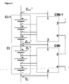
- the stack of power cells comprises the power cells C1 (8), ...Ci-1 (12), Ci (13), ...Cn (14) that are series connected, i.e. the negative terminal Ci-1 - of the power cell Ci-1 is connected to the positive electrode Ci + of the adjacent power cell Ci.
- the positive terminal C1 + of the cell C1 is the positive terminal of the stack of power cells and the negative terminal Cn - of the cell Cn is the negative terminal of the stack of power cells.
- a monitoring device CMi is associated with each power cell Ci to monitor characteristics of the power cell (temperature, voltage, ). Every monitoring device CMi is powered by the power cell Ci it is associated with, e.g. the positive supply terminal ( 1 ) of the device CMi is connected to the positive terminal Ci + of the power cell Ci and the negative supply terminal (2) of device CMi is connected to the negative terminal Ci- of the power cell Ci.
- Positive terminal Ci + and negative terminal Ci- must be understood as meaning V(Ci + ), the potential at the terminal Ci + , being higher than V(Ci - ), the potential at the terminal Ci - .
- the monitoring device CMi monitors the status of the cell Ci (e.g.
- the monitoring devices are daisy chained: the output port (4) of a monitoring device CMi-1 is connected to the input port ( 3 ) of the adjacent monitoring device CMi through a single wire (or communication link) ( 6 ).
- monitoring devices signalling devices or node indiscriminately to refer to a monitoring device CMi exchanging data with its neighbouring monitoring devices CMi+1, ... as described throughout this document.
- the potential at the positive electrode Ci + (negative electrode Ci - ) of a battery cell Ci varies in function of the index i , i.e. in function of the position of the cell in the stack, in a staircase fashion (see figure 2 ).
- the difference of potential between the positive supply voltage of a device CMi-1 and the negative supply voltage of an adjacent device CMi is the sum of the voltage differences seen by device CMi and CMi-1 respectively.
- the voltage signals generated at the output terminal ( 4 ) of a device CMi-1 and applied at the input port ( 3 ) of device CMi may be lower than the negative supply terminal of device CMi-1, imposing voltage differences (i.e. electrical stresses) higher than V(Ci-1 + ) - V(Ci-1 - ), e.g. as high as V(Ci-1 + ) - V(Ci - ).
- the voltage swing for CMi-1at the output (4) stays in the range of V(Ci-1 + ) - V(Ci-1 - ) and this valid for all cells in the daisy chain also for cell C1 and Cn.
- Every cell within the daisy chain will have the same voltage swing at their outputs independent of their place in the chain, and as a consequence, every output (4) for of the device CMi will give exactly the same load for the power cell Ci.
- the present invention proposes a signaling system that allows the transmission of data between adjacent monitoring devices CMi-1 and CMi while keeping the output (4) of the monitoring devices within operating margins contrary to solutions known to the art. This part of the invention simplifies the implementation of the output and makes the signaling more robust to disturbances in the harsh automotive environment.
- the present invention proposes a signaling system for use with a plurality of power cells (Ci-1, Ci,) each cell having a different supply voltage interval ((V(Ci-), V(Ci+)) and each cell having its respective signalling device (CMi) and whereby each signalling device (CMi) is powered by the correspondent power cell (Ci), the signaling system comprising:
- the means for limiting the variation of electrical potential at output terminal ( 4 ) of the (i-1)th signaling device (CMi-1) comprise a resistor Rbi ( 24 ) and a current source Srci( 25 ).
- the output of at least one signaling device is powered by a supply voltage VCCi-1 and a local ground voltage GNDi-1, the supply voltage and the ground voltage being generated by a DC-DC voltage converter using the cell voltages V(Ci-1+) and V(Ci-1-) or whereby at least one signaling device is powered directly by its corresponding cell voltages V(Ci-1+) and V(Ci-1-).
- the supply voltage V(VCCi-1)- V(GNDi-1) of the output-stage (4), generated by the DC-DC voltage converter can be higher or lower then the cell-voltage V(Ci-1+) - V(Ci-1-).
- the corresponding input-stage of the device Cmi comprises adapted values for Rbi and Srci to guarantee correct operation of comparator (27) of device Cmi.
- the invention also proposes a system for monitoring a plurality of power cells comprising a signaling system as proposed here above.
- a monitoring system may comprise ( figure 6 ):
- the invention further relates to a signalling method for use with a plurality of power cells (Ci-1, Ci,) each cell having a different supply voltage interval ((V(Ci-), V(Ci+)) and each cell having its respective signalling device (CMi) and whereby each signalling device (CMi) is powered by the correspondent power cell (Ci), the signaling method comprising:
- the method may comprise a limiting of the variation of said electrical potential at the input of a comparator (27) by means of a resistor and a current source.
- the invention relates also to a method of monitoring a plurality of power cells, the method using a central monitoring device ( 29 ) and a series of decentralized monitoring devices, each decentralized monitoring device being coupled to a corresponding power cell and comprising its respective signaling device where by the monitoring method further makes use of the signaling method described above.
- the monitoring method may also comprise the step of determining the first monitoring device among the decentralized monitoring devices.
- such a monitoring method may also comprise the step of assigning an address to each of the decentralized monitoring devices.
- such a monitoring method may also comprise the step of updating a control bit in the address of each decentralized monitoring device.
- a device A coupled to a device B should not be limited to devices or systems wherein an output of device A is directly connected to an input of device B. It means that there exists a path between an output of A and an input of B which may be a path including other devices or means.
- the power cells could be battery cells, photovoltaic cells, thermoelectric cells or fuel cells as well as any other device generating voltage or current.
- the power cells are (electrochemical) batteries.
- every power cell develops the same voltage difference (or electromotive force) VC between its negative electrode and its positive electrode.
- the power cells are stacked or in other words series connected to generate a voltage difference greater than that generated by a single power cell.
- the negative electrode of the battery cell C1 ( 8 ) is connected to the positive electrode of battery cell C2 ( 9 ), the negative electrode of battery cell C2 ( 9 ) is connected to the positive electrode of battery cell C3 ( 10 ) and so on.
- the power cells Ci are monitored by monitoring devices CMi i.e. devices that may monitor one or several of the parameters characterizing a power cell Ci e.g. its temperature, the difference of potential between its positive and negative terminals Ci + and Ci - , ...
- monitoring devices CMi i.e. devices that may monitor one or several of the parameters characterizing a power cell Ci e.g. its temperature, the difference of potential between its positive and negative terminals Ci + and Ci - , ...
- a monitoring device may monitor a single power cell (see figure 1 ) or a group of two or more adjacent power cells (see figure 3 ).
- the word "cell” is used in the description or in the claims, then one or more cells are meant, whereby the different cells may be connected in series or in parallel, or in series parallel.
- the monitoring devices are supplied by the power cell or group of power cells they monitor, i.e. each monitoring device CMi draws power from the positive terminal Ci + and negative terminal Ci - of the power cell it monitors, or when it monitors a group of power cells elements, it draws power from the positive terminal at the highest potential and the negative terminal at the lowest potential in said group of power cells elements.
- each monitoring device CMi draws power from the positive terminal Ci + and negative terminal Ci - of the power cell it monitors, or when it monitors a group of power cells elements, it draws power from the positive terminal at the highest potential and the negative terminal at the lowest potential in said group of power cells elements.
- the ith power cell has its positive electrode connected to the negative electrode of the (i-1)th power cell and its negative electrode connected to the positive electrode of the (i+1)th power cell.
- the same index i will be used to designate the ith monitoring device and the ith power cell it monitors.
- the index i will designate that group of battery cells as can be seen in figure 3 , Ci + the positive terminal at the highest potential in that group of power cell elements and Ci - the terminal at the lowest potential in that group of battery cells.
- V(Ci + ) will thus be the potential of the positive supply of the ith monitoring device CMi and V(Ci - ) the potential of the negative supply terminal of the ith monitoring device CMi.
- a monitoring device may contain actuators, in particular switches, capable of shunting a power cell (or a power cell element), logic or binary data processing means in the form of Digital Signal Processing unit and/or microprocessor and/or micro-controller and/or state machine and/or combinatorial logic. In the following we will refer to any such block as "logic".
- the monitoring devices may or may not contain analog data processing means in the form of analog filters, amplifiers, level shifters, .. as well as any other circuitry to generate a voltage or current reference, analog to digital converter (ADC) and/or digital to analog converter (DAC), DC-DC converter to generate auxiliary supply voltage(s).
- the monitoring devices comprise communication means to communicate the measured parameters to adjacent monitoring devices and/or a central management unit (micro-controller, micro-processor, computer, ).
- the communication means of the monitoring device comprise an input port IN ( 3 ) to receive messages and an output port OUT ( 4 ) to send messages.
- Incoming messages on input port 3 are received by a receiver 15 converting the incoming signal into data R x that can be interpreted by logic circuitry 181 included in the general analog and/or digital circuitry 18 .
- the signals generated within the general analog and/or digital circuitry 18 of a monitoring device often requires to be shared with other monitoring devices and/or a central management unit. These signals can be data R x received by the logic circuitry 181 of an ith monitoring device and that must be relayed to other monitoring nodes and/or a central management unit 29.
- These signals can also be data generated on the monitoring node: data generated by house keeping circuitry 182 and pertaining to the monitoring node itself (address, status, results of self-test procedure(s), temperature%), data acquired by a signal acquisition and processing block 183 within the monitoring node concerning signals generated by external sensors (not shown) and connected to the monitoring node by ports 19, 20, 21, ... or by internal sensors included in an internal sensor block 184 or data acquired by the signal acquisition and processing block 183 and related to the voltages V(Ci + ) and V(Ci - ) (and the voltage of intermediary nodes of the battery cell when a single monitoring device monitors two or more power cells elements as seen in figure 3 ).
- a DC-DC voltage converter 185 uses the voltages V(Ci + ) and V(Ci - ) to generate a supply voltage VCCi and provide a local reference ground voltage GNDi used to power the circuitry 18 and/or the receiver 15 and the transmitter 14 .
- the problem with the transmission of data between monitoring devices originates in that said monitoring devices operate at different supply levels/ different reference voltages.
- the (i-1)th monitoring device CMi-1 operates between the supply voltages V(Ci-1 + ) and V(Ci-1 - ) while the ith monitoring device CMi operates between the supply voltages V(Ci + ) and V(Ci - ).
- the prior art proposes to transmit signals (between two adjacent monitoring devices) through use of an open source MOSFET with the disadvantage that the voltage between drain and source of said MOSFET may be as high as V(Ci-1 + ) - V(Ci - ).
- the transmitter 14 and the receiver 15 may be, for example, as shown in figure 5 .
- the transmitter 14 of an (i-1)th monitoring node CMi-1 comprises circuitry 23 that drives a switch, in particular a transistor switch Qi-1 16 that can be a field effect transistor (MOSFET or JFET) or a bipolar transistor.
- a transistor switch Qi-1 16 that can be a field effect transistor (MOSFET or JFET) or a bipolar transistor.
- MOSFET field effect transistor
- the transistor switch Qi-1 16 is an n-type MOSFET.
- the source electrode of the n-type MOSFET transistor 16 is connected to the local GND supply i.e. GNDi-1.
- the drain electrode of the n-type MOSFET transistor Qi-1 16 is connected to the local supply voltage VCCi-1 through a pull-up resistor Ra i-1 17 . Be R1 the resistance of resistor 17 .
- the gate electrode of the n-type MOSFET transistor 16 is connected to circuitry 23 that converts signals 22 generated by general analog and/or digital circuitry 18 of the monitoring device into signals appropriate to drive the transistor 16 .
- the circuitry 23 might be a single wire connecting the circuitry 18 to the control electrode of transistor 16 or it might be a circuit that will amplify and/or shape and/or buffer and/or shift the voltage level of the signals 22 .
- the signals 22 are typically binary signals assuming either a lower voltage value L or a higher voltage value H, both lower voltage value and higher voltage value being within the interval [GNDi-1, VCCi-1]. Responding to a lower voltage value at its input, the circuitry 23 will apply to the gate of transistor 16 a voltage such that transistor 16 will be opened.
- the pull-up resistor 17 will pull the voltage on the output port 4 to a voltage higher than GNDi-1 but lower than VCCi-1.
- the circuitry 23 will apply to the gate of transistor 16 a voltage such that transistor 16 will be closed. In that case, transistor 16 will force the voltage on the output port 4 to a voltage substantially equal to GNDi-1.
- the voltage signal generated on the output port 4 of the (i-1)th monitoring device CMi-1 is applied to the input port 3 of the ith monitoring device CMi through a conducting wire 6 .
- the receiver block 15 of the ith monitoring node comprises a comparator 27 with a first and a second input, a current source 25 and a resistor 24 .
- the comparator 27 is supplied by power supplies within the interval VCCi and GNDi.
- the input port 3 of the ith monitoring device CMi is connected to a first input of the comparator 27 through a resistor Rb i 24 .
- a reference voltage Vref higher than the potential of GNDi and lower than VCCi is applied to a second input of comparator 27 .
- a current source Src i 25 forces a current I B through the resistor 24 (the switch SWi 26 is assumed to be closed).
- the resulting voltage on the first input of comparator 27 is equal to the voltage Vin of the input port 3 minus the voltage drop across the resistor 24, said voltage drop being proportional to the current I B and the resistance value R2 of resistor Rb i 24 .
- the current I B , the resistance value of resistor 24 and the voltage Vref are chosen so that (a) the potential at the first input of comparator 27 e.g. V(+) will be lower than Vref when the transistor Qi-1 16 of the (i-1)th monitoring device CMi-1 is in a first of two states (open or closed) and (b) the potential at the first input of comparator 27 will be higher than Vref (but lower than VCCi) when the transistor 16 of the ith monitoring device is in a second of said two states (open or closed).
- the product R2 X I B is taken equal to V(Ci+) -V(Ci-) (or V(VCCi) - V(GNDi)).
- the voltage at the first input of the comparator 27 is kept well within the voltage limit at which that comparator can operate without compromising proper operation and/or long term reliability, and the binary data Rx 28 generated at the output of comparator 27 varies within a voltage interval that is compatible with the general analog and/or digital circuitry 18 of the device CMi.
- the current I B and the resistance value R2 of resistor 24 and R1 of resistor 17 are chosen so that the voltage drop across resistor 24 is substantially equal to VC and the voltage drop across resistor 17 is small compared to VC.
- V(+) will vary from substantially V(GNDi) when the transistor Qi-1 16 is closed to substantially VCCi when the transistor Qi-1 16 is open.
- the voltage at the output (4) of the (i-1)th monitoring device will vary between GNDi-1 and a voltage substantially equal to VCCi-1 (strictly speaking this voltage will be equal to VCCi-1 - R1 X IB as can be deducted from equation 1).
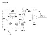
- the condition R2 X IB VC is advantageously realized with a current source Srci 25 as seen on figure 11 .
- the reference bias current IB is generated with a MOSFET transistor M1 and a resistor 110 that has the same resistance R2 as resistor Rb i .
- Transistor M1 is connected in diode manner and is connected in series with the resistor R1 between VCCi and GNDi.
- the current in the resistor 110 is equal to (VCCi - VDS - GNDi) / R2 where VDS is the voltage drop between drain and source of transistor M1. In a first approximation, that current will be equal to (VCCi-GNDi)/R2.
- the current is mirrored through transistor M2 and M3 to transistor M4.
- transistor M4 acts as current source and forces the current IB to flow through resistor Rbi 24.
- the current IB in transistor M4 is equal to the current in the resistor 110.
- the voltage difference between a first and a second main electrode of transistor Qi-1 16 is kept below VC (i.e. the transistor 16 is not exposed to electrical stress that would affect proper operation and/or long term reliability) as can be seen from Equations 1 to 4 here above.
- the voltage at the output port 4 of every monitoring node CMi will remain within the interval [V(Ci - ), V(Ci + )].
- the monitoring devices CMi according to this invention send data in a fashion compatible with communication protocols known to the art, in particular the LIN protocol, without the need for opto-couplers between the monitoring devices CMi-1 and CMi.
- This also implies that the supply-current related to the transmitter will be the same for all outputs (4) because all outputs will have the same voltage-swing.
- the transmitter 14 and receiver 15 described here above can be used advantageously to identify the first monitoring device CM1 in a series of daisy chained monitoring devices CMi.
- data must be exchanged not only between monitoring devices but also between the monitoring devices and a central management unit 29.
- the data management unit could use the transmitter 14 and/or the receiver 15 to exchange data with the first or the last monitoring device.
- one of the monitoring devices on figure 1 could assume the role of a central management unit in addition to its role as a monitoring device.
- the central management unit will not have a common supply with any of the monitoring devices or it will not be practical to impose that data be exchanged between the central management unit and a monitoring device without isolator. This will be the case for instance when the monitoring devices are mass produced and substantially identical, i.e. the resistance value R1 and R2 of resistor 17 and 24 and the current I B sourced by current source 25 remaining substantially unchanged from monitoring device to monitoring device.
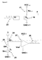
- the monitoring unit CM1 associated with the battery cell C1 ( 8 ) receives data ( 5a, 5b ) from a central management unit 29 that drives an opto-coupler 30 (the coupler 30 could also be any other electrical isolator-couplers based on e.g. optical or magnetic interconnection).
- a pull-up resistor 31 (connected to C1 + or as proposed below to VCC1) is necessary for the proper operation of the opto-coupler 30.
- a second opto-coupler 32 is driven by the last monitoring device to allow it to send data to the central data management unit 29.
- Information can be send from the central data management unit 29 to any monitoring device CMi by transiting through CM1, CM2, ...CMi-1.
- Data can be send from any device CMi and reach the central data management unit 29 by transiting through CMi+1, ..., Cn and the opto-coupler 32.
- the current level of the data signals 5a vary between a lower value and a higher value (sufficient to deactivate or activate the opto-coupler 30 ) as is the case when digital data is sent by the central management unit 29, current will not flow or flow through the pull up resistor 31 .
- the voltage on the input port 3 of the monitoring unit CM1 associated with the battery cell 8 varies from a voltage substantially equal to the supply V(C1+) of that monitoring device to a voltage substantially equal to GND1. This will be true whether the switch 26 from the receiver 15 of CM1 is open or closed.
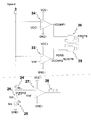
- the device CMi if the voltage at which data is received on the input port 3 of monitoring device CMi does not exceed VCCi (or V(Ci + ), the device CMi is the device CM1, first in the daisy chain of devices CMi, operating at the highest supply voltage V(C1 + ) and associated with the first power cell C1. If the voltage at which data is received on the input port 3 of monitoring device CMi exceeds VCCi when data is transmitted, the device CMi is not the first in the daisy chain of devices CMi.
- a resistor may be used in parallel with the pull-up resistor Rai (17) of every monitoring device CMi that is not the first. This situation is illustrated on figure 7 where the pull-up resistor 31 is connected to VCCi. For CM1, the resistor 31 is used for the opto-coupler (30). This implementation makes sure that any monitoring device CMi will have the same load for Ci. For all CMi, the pull-up resistors will see the same voltage difference V(Ci) independent of the cell C1 or any other cell. When the monitoring devices are integrated circuits, resistor 31 is connected to VCCi and an auxiliary port "Aux".
- the Aux port of the first device CM1 is connected to the opto-coupler 30 (as shown on figure 7 ).
- the auxiliary port ios shorted with the output port 4 (see figure 7 ).
- Comparator 34 compares Vin(i) with VCC(i) (alternatively it compares the result to VCCi + ⁇ V where 0 ⁇ ⁇ V ⁇ VC). This can be done for instance by dividing the input Vin(i) with a resistive divider and comparing the result with a divided (with the same ratio) version of VCCi (or VCCi+ ⁇ V), or any other method or circuit known from the art. Be VCOMP1 the result of the comparison made by comparator 34.
- Comparator 33 compares Vin(i) with a reference voltage Vref such that GNDi ⁇ Vref ⁇ VCC(i). Be VCOMP2 the result of the comparison made by comparator 33.
- Vref a reference voltage
- the output of COMP1 will always be low: indeed Vin(1) is always ⁇ VCC1 (hence it is smaller than VCC1 + ⁇ V).
- the output of COMP2 will vary between a low state L and high state H indicating that data is being received by CM1.
- the switch SW1 ( 26 ) remains open and no current IB is forced through the resistor Rb1.
- the voltage at the inputs of comparator ( 27 ) varies between GND1 and VCC1.
- the combination of the signals VCOMP1 and VCOMP2 that will determine whether or not the monitoring device CMi is the first in the daisy chain and whether or not to close the switch SWi ( 26 ) (to force current through resistor Rbi 24 ) is done by any appropriate logic circuitry according to techniques known to the art (an example of such circuit will be given below).
- WO 00/05596 a unique address is given to each monitoring device through use of a dip switch that is manually configured. If most of the monitoring device has been integrated in a semiconductor chip, the use of dip switch would also imply additional dedicated connection pins on that chip that are not always desired or even not available.
- the first monitoring device in the daisy chain is assigned an address by a master e.g. a central data management unit 29 or assign itself a first address. Addressing the other monitoring devices may then proceed in a number of ways known to the art. For instance, once a monitoring device is known to be the first/knows that it is the first, it may proceed by issuing a message to the next monitoring device to signal that device that it is the second in the daisy chain. That second monitoring device may then proceed by issuing a message to the next monitoring device to signal that device that it is the third in the daisy chain and so on. For an other embodiment of the invention, the address assignment can happen under the control of the central data management unit 29 .
- the central data management unit will issue the required messages to assign the address to the different monitoring devices.
- no monitoring devices will have an address and will not communicate the received data at input (3) to their output (4).
- the command of the central data management unit 29 will only arrive at the first monitoring device and will get its address.
- the monitoring unit will enable his output (4) so that the next messages will also arrive at the next monitoring unit.
- the next message of the central data management unit 29 can assign the address to the next monitoring unit. Repetition of these steps will assign an address to every monitoring module and will close the communication loop though the last monitoring unit CMn. Since the order of the monitoring devices corresponds to the order of the battery/power cells in the stack of battery/power cells, it is possible to associate the information of an ith monitoring node to the ith battery/power cells it monitors.
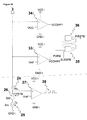
- each node is important for the proper operation of the monitoring system and in particular it is of utmost importance to clearly identify which node is the first and which nodes are not first in the daisy chain: failure to do so might prevent reception of an incoming message. Indeed, if a node is incorrectly identified as first in the daisy chain, the switch Swi 26 (see figure 8 ) will not be activated and the output of comparator 27 will never vary. If the first node in the daisy chain is incorrectly considered to be further in the daisy chain (i.e assumed not to be the first), the switch Sw1 will be activated, the input of comparator 27 will be stuck to GND1 and the output of comparator will not vary either.
- FIRSTB a control bit found in every node of the daisy chain.
- FIRSTB is High if the node is not the first node in the daisy chain.
- FIRSTB is low if the node is first in the daisy chain.
- the switch Swi 26 is closed if FIRSTB is high and the Swi 26 is open if FIRSTB is low.
- FIRSTB is set to low by default and the switch Swi 26 is open for every node in the daisy chain.
- a possible implementation of a logical circuit that will update the value of FIRSTB accordingly is given on figure 9 .
- a first 2 input NAND gate 36 and a second three input NAND gate 35 are connected as an RS flip-flop.
- One of the input of the NAND gate is driven by a power on reset signal that will initialize FIRSTB to Low.
- the state of FIRSTB might be altered by a disturbance during operation of the system. This would prevent the node for which the value of FIRSTB has been altered to properly receive data.
- the disturbance might for instance be caused by an ionizing radiation or by a neutron that will interact with the semiconductor substrate and generate a cascade of charged particles.
- the origin of the ionizing radiation or neutron may be artificial or natural (cosmic rays for instance).
- the disturbance can also be caused by EMC-disturbance e.g. RF-signals that are received by the connection 6 (see e.g. figure 1 ) between 2 cells.
Abstract
Description
- The present invention relates to power cells and methods of manufacturing and operating power cells. In particular the invention relates to a signaling system and method that is applicable for use in a system for monitoring and/or controlling a stack of power cells, e.g. of a battery.
- Monitoring of individual battery elements or group of battery elements in a set of series connected batteries or series connected group of batteries is known from the art.
US 6,891,352 describes a battery apparatus for controlling battery modules connected in series, the battery apparatus to be used for electric car or hybrid electric car. So called lower order control devices control battery modules having plural battery cells connected in series. Data is exchanged between lower order control devices and a so called high order control device that gives instructions to the lower order control devices.
A lower order control device draws power from the battery module it monitors. Data is transmitted from the high order control device to any of the lower order control device through a daisy chain: a first lower order control device receives data from the high order control devices through an opto-insulator (also known as photocouplers or opto-isolators). The message received may be relayed to a second lower order control device without the need for an opto-isolator, that in turns may relay the message to a third lower order control device and so on. The lower order control devices operating at different voltages, problems may arise when transmitting data from one lower order control device to another. To overcome that problem without use of an opto-insulator for isolating two successive lower order control devices, the configuration adopted inUS 6,891,352 to connect two adjacent lower order control devices relies on the establishment of a current loop between said two adjacent lower order control devices. On the daisy chained seen onfigure 1 ofUS 6,891,352 , the communication takes place from the top-low order control device IC-1 to the bottom low order control device IC-3. The device IC-1 sources a current from VDD to an output Out-1. Device IC-2 will receive this current at its input In-1. The voltage swing at the output Out-1 is defined by the components in device IC-1 and the components in device IC-2. Matching of the components between these 2 different devices will determine the signal amplitude. The diodes used as protection act as rectifiers and affects the EMC-performance of the device. Such implementation is not desired in an harsh automotive environment.
In battery monitoring systems, it is important that every battery modules sees the same electrical load. This is important to keep the same condition for every battery module so that no battery module will be discharged faster then the other battery modules. This is not the case in theUS 6.891.352 patent. Indeed, the top battery module (VB1, VB2, VB3, VB4) supplying the control device IC-1has an extra load in the form of opto-couplers F1, F2, F3 ans the associated pull-up resistors RF1, RF2, RF3. The battery module (VB5, VB6, VB7, VB8) is loaded by the control device IC-2 only while the bottom battery module (VB9, VB10, VB11, VB12) is loaded by the control device IC-3 as well as by the opto-couplers F4, F5, F6. This problem will be solved by the invention.
WO 00/05596 US 6,891,352 each said cell monitoring device is powered by the battery cells it monitors and as a consequence, two monitoring devices will usually operate at different voltages. Be VCC1 the positive supply voltage of a first monitoring device and GND1 the negative supply voltage of that first monitoring device. Be VCC2 the positive supply voltage of a second monitoring device adjacent to said first monitoring device and GND2 the negative supply voltage of that second monitoring device. The supplies of the monitoring devices are "stacked", i.e. VCC1> GND1 = VCC2> GND2. The first and second monitoring devices operate at different voltage levels. When the voltage differences become important, it may become impossible to transmit messages from the first monitoring device to the second without opto-insulator. In order not to have to use opto-isolators (or any other component that allows the transmission of data while guaranteeing galvanic isolation),WO 00/05596
When the micro-controller in the first monitoring device output a voltage high on the gate of P-MOSFETQ (high voltage between source and gate), P-MOSFET Q is switched on and a current flows from VCC1 through resistors R1, R2 and R3 to the ground GND2 of the second cell monitoring device. As a result, the voltage (VCC1 - GND2) x (R3)/(R1+R2+R3) is applied to the first input of COMP2 to be compared with VREF2. Provided the value of VREF2 is between the voltage levels applied to the first input of comparator COMP2 when P-MOSFET Q is switched ON and OFF, the output of comparator COMP2 will be a square wave signal varying in a voltage interval between the supply potentials GND2 and VCC2 of the second monitoring device. Therefore messages encoded within the variation of the signal applied to the gate of P-MOSFETQ are transferred from the first monitoring device to the second monitoring device.
One sees that the potential at the drain of P-MOSFET Q will vary between approximately VCC1 (when MOSFETQ is switched on) and GND2 (when MOSFET Q is switched off). Hence the voltage difference between drain and source of MOSFET Q will vary between 0 and (VCC1-GND2). The potential difference between VCC1 and GND2 will vary in function of the type of batteries being monitored as well as the number of battery cells monitored by each monitoring device. It will also vary in function of the level of charge of the battery elements. In practical applications, the difference of potential between VCC1 and GND2 may be higher than 60 volts. In those cases, the integration of the micro-controller and MOSFETQ on the same silicon substrate, may become difficult or even impossible depending on the integration technologies available. It would therefore be beneficial to limit the voltage difference between the drain electrode and the source electrode of MOSFETQ in particular and any other transistor involved in the transmission of information between monitoring devices in general. - One also sees that provided the signals applied to the gate of MOSFTQ by the micro-controller in the first monitoring device vary between GND1 and VCC1, the difference of potential between the gate electrode and the source electrode of MOSFET Q will at least be equal to V(GND1) - V(GND2). If MOSFETQ is an n-type MOS and V(GND1) - V(GND2) is substantially higher than the threshold voltage of MOSFETQ, it will be impossible to switch MOSFETQ off. Current will continuously flow through MOSFETQ as well as resistors R1, R2 and R3. Since in any given technology, a MOSFET transistor has a given threshold voltage that may be lower than V(GND1) - V(GND2), it would be beneficial to limit the variation of potential of the source electrode of MOSFET Q in particular and any other transistor involved in the transmission of information between monitoring devices in general so that MOSFETQ can be switched off whatever the difference V(GND1) - V(GND2) might be.
- Identification of the monitoring devices is important to allow detection of faulty battery cells and/or faulty monitoring devices by the central battery monitoring system. While both
US 6,891,352 andWO 00/596 WO 00/05596 - An object of the present invention is to provide improved power cell arrangements. An advantage of at least some of the embodiments of the present invention is avoiding at least one of the problems identified in the prior art. First, in some embodiments it reduces the voltage difference between two electrodes of a transistor switch involved in the transmission of data between two monitoring devices that operate at different supply voltage levels. Embodiments of the invention can allow the integration on the same semiconductor substrate of most of the components necessary for a monitoring device: digital processing circuitry and/or microprocessor and/or micro-controller and/or analog to digital and digital to analog converters, voltage and current references, amplifiers, protection circuitry protecting against e.g. electrostatic discharges, reverse polarity, voltage surges, ... together with one or more transistor switches involved in the transmission of data between two monitoring devices operating at different supply voltage levels. Embodiments of the invention can allow identification of a first monitoring device, said first monitoring device receiving data directly from a central monitoring device and the identification of any other device in the daisy-chain. The identification of the first device is based on a combination of signals generated by each monitoring devices. It does not require human intervention or components like DIP switches and allows the use of the same circuit, in particular integrated circuit, for any monitoring node. In particular, the identification of the first monitoring device in a chain of daisy chained monitoring devices makes use of the specificities of the communication interface that allows transmission of data between two monitoring devices operating at different supply voltage levels. The identification of the other devices is realized under control of the higher order device.
Thirdly, embodiments of the present invention can allow the use of communication protocols that are standard communication protocols for automotive applications.
The invention also guarantees that every battery cell in a stack of series connected battery cells will see the same load also when extra isolator-couplers (e.g an opto-isolator) are required for the communication (e.g. for the first monitoring device and the last monitoring device). - The invention relates to a signaling system that is applicable for use in a system for monitoring and/or controlling a stack of power cells. The power cells may be photovoltaic cells, thermo-photovoltaic cells, fuel cells, battery cells, ... As seen in
figure 1 , the stack of power cells comprises the power cells C1 (8), ...Ci-1 (12), Ci (13), ...Cn (14) that are series connected, i.e. the negative terminal Ci-1- of the power cell Ci-1 is connected to the positive electrode Ci+ of the adjacent power cell Ci. The positive terminal C1+ of the cell C1 is the positive terminal of the stack of power cells and the negative terminal Cn- of the cell Cn is the negative terminal of the stack of power cells.
A monitoring device CMi is associated with each power cell Ci to monitor characteristics of the power cell (temperature, voltage, ...). Every monitoring device CMi is powered by the power cell Ci it is associated with, e.g. the positive supply terminal (1) of the device CMi is connected to the positive terminal Ci+ of the power cell Ci and the negative supply terminal (2) of device CMi is connected to the negative terminal Ci- of the power cell Ci. Positive terminal Ci+ and negative terminal Ci- must be understood as meaning V(Ci+), the potential at the terminal Ci+, being higher than V(Ci-), the potential at the terminal Ci-.
The monitoring device CMi monitors the status of the cell Ci (e.g. it measures the difference of potential between the positive terminal Ci+ and the negative terminal Ci-of that cell but it may also measure the temperature of the power cell Ci, the pH of the electrolyte if the power cell Ci is a battery, ...) and communicates information on the status of the cell Ci to other monitoring devices. In the present invention, the monitoring devices are daisy chained: the output port (4) of a monitoring device CMi-1 is connected to the input port (3) of the adjacent monitoring device CMi through a single wire (or communication link) (6). Data cannot be exchanged between a monitoring device CMi and a monitoring device CMi+k (with k>1) without that the data sent by the device CMi transit by the devices CMi+1, CMi+2, ..., CM i+k-1 (i and k being integer numbers of course). In the following, we will use the terms monitoring devices, signalling devices or node indiscriminately to refer to a monitoring device CMi exchanging data with its neighbouring monitoring devices CMi+1, ... as described throughout this document.
The potential at the positive electrode Ci+ (negative electrode Ci-) of a battery cell Ci varies in function of the index i , i.e. in function of the position of the cell in the stack,
in a staircase fashion (seefigure 2 ). As is evident fromfigure 2 , the difference of potential between the positive supply voltage of a device CMi-1 and the negative supply voltage of an adjacent device CMi is the sum of the voltage differences seen by device CMi and CMi-1 respectively. This is not without consequences for the electronic components used to build the monitoring devices CM and in particular transistor switches involved in the data transmission from device to CMi-1 to device CMi. - In the prior art, adjacent devices operating at different supply voltages (different reference voltages), the voltage signals generated at the output terminal (4) of a device CMi-1 and applied at the input port (3) of device CMi may be lower than the negative supply terminal of device CMi-1, imposing voltage differences (i.e. electrical stresses) higher than V(Ci-1+) - V(Ci-1-), e.g. as high as V(Ci-1+) - V(Ci-). For the invention, the voltage swing for CMi-1at the output (4) stays in the range of V(Ci-1+) - V(Ci-1-) and this valid for all cells in the daisy chain also for cell C1 and Cn. As such, every cell within the daisy chain will have the same voltage swing at their outputs independent of their place in the chain, and as a consequence, every output (4) for of the device CMi will give exactly the same load for the power cell Ci.The present invention proposes a signaling system that allows the transmission of data between adjacent monitoring devices CMi-1 and CMi while keeping the output (4) of the monitoring devices within operating margins contrary to solutions known to the art.
This part of the invention simplifies the implementation of the output and makes the signaling more robust to disturbances in the harsh automotive environment. - The present invention proposes a signaling system for use with a plurality of power cells (Ci-1, Ci,) each cell having a different supply voltage interval ((V(Ci-), V(Ci+)) and each cell having its respective signalling device (CMi) and whereby each signalling device (CMi) is powered by the correspondent power cell (Ci), the signaling system comprising:
- at least, an (i-1)th and a ith signalling device (CMi-1, CMi),
- a communication link (6) for transmitting signals from an output terminal (4) of said (i-1)th signalling device (CMi-1) to an input terminal (3) of said ith signalling device (CMi)
- said communication link consisting of an electrical conducting connection;
- said (i-1)th signalling device (CMi-1) comprises means (
Fig. 6 : Qi-1 16, Ra i-1 17) for varying the electrical potential at said output terminal (4) in dependence upon the signal to be transmitted, - said ith signaling device (CMi) comprises means for sensing, (comparator 27), via said communication link (6) and said input terminal (3), the variation of potential of said output terminal (4) and for outputting a signal (28) which varies in dependence upon the sensed variation of potential and that
- In particular, the means for limiting the variation of electrical potential at output terminal (4) of the (i-1)th signaling device (CMi-1) comprise a resistor Rbi (24) and a current source Srci(25).
According to another embodiment of the invention (figure 4 ,5 ), the output of at least one signaling device is powered by a supply voltage VCCi-1 and a local ground voltage GNDi-1, the supply voltage and the ground voltage being generated by a DC-DC voltage converter using the cell voltages V(Ci-1+) and V(Ci-1-) or whereby at least one signaling device is powered directly by its corresponding cell voltages V(Ci-1+) and V(Ci-1-). The supply voltage V(VCCi-1)- V(GNDi-1) of the output-stage (4), generated by the DC-DC voltage converter can be higher or lower then the cell-voltage V(Ci-1+) - V(Ci-1-). The corresponding input-stage of the device Cmi comprises adapted values for Rbi and Srci to guarantee correct operation of comparator (27) of device Cmi. - The invention also proposes a system for monitoring a plurality of power cells comprising a signaling system as proposed here above. In particular, such a monitoring system may comprise (
figure 6 ): - a central monitoring device (29) and a series of decentralized monitoring devices, each monitoring device comprising a correspondent signaling device (CMi),
- an isolator (30) to couple an output terminal of said central monitoring device to an input terminal (3) of the first monitoring device / signaling device CM1 and where the isolator (30) limits the voltage variations at the input terminal of the first monitoring device below the highest supply voltage of the first battery cell (V(C1+)) and above the lowest supply voltage of the first battery cell (V(C1-)).
- The invention further relates to a signalling method for use with a plurality of power cells (Ci-1, Ci,) each cell having a different supply voltage interval ((V(Ci-), V(Ci+)) and each cell having its respective signalling device (CMi) and whereby each signalling device (CMi) is powered by the correspondent power cell (Ci), the signaling method comprising:
- transmitting signals from an output terminal (4) of said (i-1)th signalling device (CMi-1) to an input terminal (3) of said ith signalling device (CMi) characterized in that the method further comprises;
- varying the electrical potential at said output terminal (4) of said (i-1)th signalling device (CMi-1) in dependence upon the signal to be transmitted, and
- limiting the variation of said electrical potential to the supply voltage interval [V(Ci-1-), V(Ci-1+)] of said (i-1)th signaling device,
- sensing at the input terminal (3) of said ith signalling device (CMi), the variation of potential of said output terminal (4) of said i-1th signalling device (CMi-1), and for outputting a signal (28) which varies in dependence upon the sensed variation of potential.
- According to an aspect of the invention, the method may comprise a limiting of the variation of said electrical potential at the input of a comparator (27) by means of a resistor and a current source.
- The invention relates also to a method of monitoring a plurality of power cells, the method using a central monitoring device (29) and a series of decentralized monitoring devices, each decentralized monitoring device being coupled to a corresponding power cell and comprising its respective signaling device where by the monitoring method further makes use of the signaling method described above. According to the invention, the monitoring method may also comprise the step of determining the first monitoring device among the decentralized monitoring devices.
- According to an aspect of the invention, such a monitoring method may also comprise the step of assigning an address to each of the decentralized monitoring devices.
- According to an aspect of the invention, such a monitoring method may also comprise the step of updating a control bit in the address of each decentralized monitoring device.
-
-
Figure 1 - Stack of batteries/power cells and daisy chain of associated monitoring devices. -
Figure 2 - Variation of voltages across the stack of batteries/power cells. -
Figure 3 - Battery cells comprising two or more battery elements and associated monitoring devices. -
Figure 4 - Monitoring device. -
Figure 5 - Signaling means of the monitoring devices : receiver and transmitter. -
Figure 6 - Battery monitoring system with central monitoring unit. -
Figure 7 - Equal loading of the battery cells -
Figure 8 - Monitoring of the signal levels for identification of the first monitoring device CM1. -
Figure 9 - Circuit for updating a control bit of an address. -
Figure 10 - Circuit for correcting the control bit in an address -
Figure 11 - Signaling means of the monitoring devices: a transmitter arangement - The present invention will be described with respect to particular embodiments and with reference to certain drawings but the invention is not limited thereto but only by the claims. The drawings described are only schematic and are non-limiting. In the drawings, the size of some of the elements may be exaggerated and not drawn on scale for illustrative purposes. The dimensions and the relative dimensions do not correspond to actual reductions to practice of the invention.
- Moreover, the terms top, bottom, over under and the like in the description and the claims are used for descriptive purposes and not necessarily for describing relative positions. It is to be understood that the terms so used are interchangeable under appropriate circumstances and that the embodiments of the invention described herein are capable of operation in other orientations than described or illustrated herein.
- It is to be noticed that the term "comprising", used in the claims, should not be interpreted as being restricted to the means listed thereafter; it does not exclude other elements or steps. It is thus to be interpreted as specifying the presence of the stated features, integers, steps or components as referred to, but does not preclude the presence or addition of one or more other features, integers, steps or components, or groups thereof. Thus, the scope of the expression "a device comprising means A and B" should not be limited to devices consisting only of components A and B. It means that with respect to the present invention, the only relevant components of the device are A and B.
- Similarly, it is to be noticed that the term "coupled", also used in the claims, should not be interpreted as being restricted to direct connections only. Thus, the scope of the expression "a device A coupled to a device B" should not be limited to devices or systems wherein an output of device A is directly connected to an input of device B. It means that there exists a path between an output of A and an input of B which may be a path including other devices or means.
- The invention will now be described by a detailed description of several embodiments of the invention. It is clear that other embodiments of the invention can be configured according to the knowledge of persons skilled in the art without departing from the true spirit or technical teaching of the invention, the invention being limited only by the terms of the appended claims.
- As seen in
figure 1 , we consider a stack of N series connected power cells C1 (8), C2 (9), C3 (10), C4 (11), ..., Ci-1 (12), Ci (13), ...Cn (14). The power cells could be battery cells, photovoltaic cells, thermoelectric cells or fuel cells as well as any other device generating voltage or current. In particular the power cells are (electrochemical) batteries. For the sake of simplicity and without restricting the scope of this invention, we may assume that every power cell develops the same voltage difference (or electromotive force) VC between its negative electrode and its positive electrode. The power cells are stacked or in other words series connected to generate a voltage difference greater than that generated by a single power cell. For instance, in the example offigure 1 , the negative electrode of the battery cell C1 (8) is connected to the positive electrode of battery cell C2 (9), the negative electrode of battery cell C2 (9) is connected to the positive electrode of battery cell C3 (10) and so on. - The power cells Ci are monitored by monitoring devices CMi i.e. devices that may monitor one or several of the parameters characterizing a power cell Ci e.g. its temperature, the difference of potential between its positive and negative terminals Ci+ and Ci-, ... In the following we will indiscriminately refer to those devices as monitoring nodes, monitoring devices, control or controlling devices, control or controlling nodes, slaves, slave units. A monitoring device may monitor a single power cell (see
figure 1 ) or a group of two or more adjacent power cells (seefigure 3 ). For the present patent, when the word "cell" is used in the description or in the claims, then one or more cells are meant, whereby the different cells may be connected in series or in parallel, or in series parallel. The monitoring devices are supplied by the power cell or group of power cells they monitor, i.e. each monitoring device CMi draws power from the positive terminal Ci+ and negative terminal Ci- of the power cell it monitors, or when it monitors a group of power cells elements, it draws power from the positive terminal at the highest potential and the negative terminal at the lowest potential in said group of power cells elements. In the following, we will identify the power cells in the stack by the index i. The ith power cell has its positive electrode connected to the negative electrode of the (i-1)th power cell and its negative electrode connected to the positive electrode of the (i+1)th power cell. The same index i will be used to designate the ith monitoring device and the ith power cell it monitors.
If the ith monitoring node is monitoring a group of series connected power cell elements, the index i will designate that group of battery cells as can be seen infigure 3 , Ci+ the positive terminal at the highest potential in that group of power cell elements and Ci- the terminal at the lowest potential in that group of battery cells. V(Ci+) will thus be the potential of the positive supply of the ith monitoring device CMi and V(Ci-) the potential of the negative supply terminal of the ith monitoring device CMi. As seen infigure 2 , the lowest the index i, the higher the potentials V(Ci+) and V(Ci-) i.e.-V(Ci+) >V(Ci-) = V(Ci+1+) >V(Ci+1). - In addition to sensors or probing means required for the measurement of the parameters of a power cell , a monitoring device may contain actuators, in particular switches, capable of shunting a power cell (or a power cell element), logic or binary data processing means in the form of Digital Signal Processing unit and/or microprocessor and/or micro-controller and/or state machine and/or combinatorial logic. In the following we will refer to any such block as "logic". The monitoring devices may or may not contain analog data processing means in the form of analog filters, amplifiers, level shifters, .. as well as any other circuitry to generate a voltage or current reference, analog to digital converter (ADC) and/or digital to analog converter (DAC), DC-DC converter to generate auxiliary supply voltage(s). The monitoring devices comprise communication means to communicate the measured parameters to adjacent monitoring devices and/or a central management unit (micro-controller, micro-processor, computer, ...).
- An example of monitoring device can be found schematically in
figure 4 . The communication means of the monitoring device comprise an input port IN (3) to receive messages and an output port OUT (4) to send messages. Incoming messages oninput port 3 are received by areceiver 15 converting the incoming signal into data Rx that can be interpreted bylogic circuitry 181 included in the general analog and/ordigital circuitry 18.
The signals generated within the general analog and/ordigital circuitry 18 of a monitoring device often requires to be shared with other monitoring devices and/or a central management unit. These signals can be data Rx received by thelogic circuitry 181 of an ith monitoring device and that must be relayed to other monitoring nodes and/or acentral management unit 29. These signals can also be data generated on the monitoring node: data generated byhouse keeping circuitry 182 and pertaining to the monitoring node itself (address, status, results of self-test procedure(s), temperature...), data acquired by a signal acquisition andprocessing block 183 within the monitoring node concerning signals generated by external sensors (not shown) and connected to the monitoring node byports internal sensor block 184 or data acquired by the signal acquisition andprocessing block 183 and related to the voltages V(Ci+) and V(Ci-) (and the voltage of intermediary nodes of the battery cell when a single monitoring device monitors two or more power cells elements as seen infigure 3 ). The outgoing messages corresponding to said signals are made available on theoutput port 4 through atransmitter 14. A DC-DC voltage converter 185 uses the voltages V(Ci+) and V(Ci-) to generate a supply voltage VCCi and provide a local reference ground voltage GNDi used to power thecircuitry 18 and/or thereceiver 15 and thetransmitter 14. In a trivial case, there is no DC-DC converter and the circuitry is powered directly from Ci+ and Ci -, i.e. VCCi = V(Ci+) and/or V(GNDi) = V(Ci-). In some application, it may be advantageous to generate VCCi such that V(Ci-).< VCCi < V(Ci+). - The problem with the transmission of data between monitoring devices originates in that said monitoring devices operate at different supply levels/ different reference voltages. Let us for instance consider the transmission of a signal from an (i-1)th monitoring device CMi-1 and an ith monitoring device CMi: the (i-1)th monitoring device CMi-1 operates between the supply voltages V(Ci-1+) and V(Ci-1-) while the ith monitoring device CMi operates between the supply voltages V(Ci +) and V(Ci-).
- As discussed earlier, the prior art proposes to transmit signals (between two adjacent monitoring devices) through use of an open source MOSFET with the disadvantage that the voltage between drain and source of said MOSFET may be as high as V(Ci-1+) - V(Ci-).
- In the present invention, the
transmitter 14 and thereceiver 15 may be, for example, as shown infigure 5 . - The
transmitter 14 of an (i-1)th monitoring node CMi-1 comprisescircuitry 23 that drives a switch, in particular a transistor switch Qi-1 16 that can be a field effect transistor (MOSFET or JFET) or a bipolar transistor. For the sake of clarity we will consider the particular case where the transistor switch Qi-1 16 is an n-type MOSFET. The source electrode of the n-type MOSFET transistor 16 is connected to the local GND supply i.e. GNDi-1. The drain electrode of the n-type MOSFET transistor Qi-1 16 is connected to the local supply voltage
VCCi-1 through a pull-up resistor Ra i-1 17. Be R1 the resistance ofresistor 17. The gate electrode of the n-type MOSFET transistor 16 is connected tocircuitry 23 that converts signals 22 generated by general analog and/ordigital circuitry 18 of the monitoring device into signals appropriate to drive thetransistor 16. To that end, thecircuitry 23 might be a single wire connecting thecircuitry 18 to the control electrode oftransistor 16 or it might be a circuit that will amplify and/or shape and/or buffer and/or shift the voltage level of thesignals 22. Thesignals 22 are typically binary signals assuming either a lower voltage value L or a higher voltage value H, both lower voltage value and higher voltage value being within the interval [GNDi-1, VCCi-1]. Responding to a lower voltage value at its input, thecircuitry 23 will apply to the gate of transistor 16 a voltage such thattransistor 16 will be opened. In that case, the pull-upresistor 17 will pull the voltage on theoutput port 4 to a voltage higher than GNDi-1 but lower than VCCi-1. Responding to a higher voltage value at its input, thecircuitry 23 will apply to the gate of transistor 16 a voltage such thattransistor 16 will be closed. In that case,transistor 16 will force the voltage on theoutput port 4 to a voltage substantially equal to GNDi-1. The voltage signal generated on theoutput port 4 of the (i-1)th monitoring device CMi-1 is applied to theinput port 3 of the ith monitoring device CMi through aconducting wire 6. Thereceiver block 15 of the ith monitoring node comprises acomparator 27 with a first and a second input, acurrent source 25 and aresistor 24. Thecomparator 27 is supplied by power supplies within the interval VCCi and GNDi.
Theinput port 3 of the ith monitoring device CMi is connected to a first input of thecomparator 27 through aresistor Rb i 24. A reference voltage Vref higher than the potential of GNDi and lower than VCCi is applied to a second input ofcomparator 27. A current source Src i 25 forces a current IB through the resistor 24 (theswitch SWi 26 is assumed to be closed). The resulting voltage on the first input ofcomparator 27 is equal to the voltage Vin of theinput port 3 minus the voltage drop across theresistor 24, said voltage drop being proportional to the current IB and the resistance value R2 ofresistor Rb i 24.
When the transistor switch Qi-1 16 of the (i-1)th monitoring device CMi-1 is open, the voltage Vin(i) at theinput port 3 of the ith monitoring device CMi and the voltage V(+) (where V(+) is the voltage at a first input of thecomparator 27 of the ith monitoring device CMi e.g. the + input as seen infigure 5 ) are such that the following equalities are satisfied:

- When the transistor switch Qi-1 16 of the (i-1)th monitoring device CMi-1 is closed, the voltage Vin(i) at the
input port 3 of the ith monitoring device CMi and the voltage V(+) (where V(+) is the voltage at a first input of thecomparator 27 of the ith monitoring device CMi e.g. the + input as seen infigure 5 ) are such that the following equalities are satisfied:

- The current IB, the resistance value of
resistor 24 and the voltage Vref are chosen so that (a) the potential at the first input ofcomparator 27 e.g. V(+) will be lower than Vref when the transistor Qi-1 16 of the (i-1)th monitoring device CMi-1 is in a first of two states (open or closed) and (b) the potential at the first input ofcomparator 27 will be higher than Vref (but lower than VCCi) when thetransistor 16 of the ith monitoring device is in a second of said two states (open or closed). In particular, the product R2 X IB is taken equal to V(Ci+) -V(Ci-) (or V(VCCi) - V(GNDi)). The voltage at the first input of thecomparator 27 is kept well within the voltage limit at which that comparator can operate without compromising proper operation and/or long term reliability, and thebinary data Rx 28 generated at the output ofcomparator 27 varies within a voltage interval that is compatible with the general analog and/ordigital circuitry 18 of the device CMi. In particular, under the assumption that the voltage difference V(Ci+) - V(Ci-) (or V(VCCi) - V(GNDi)) has substantially the same value VC for every monitoring node, the current IB and the resistance value R2 ofresistor 24 and R1 ofresistor 17 are chosen so that the voltage drop acrossresistor 24 is substantially equal to VC and the voltage drop acrossresistor 17 is small compared to VC. In that case, for the ith monitoring device, V(+) will vary from substantially V(GNDi) when the transistor Qi-1 16 is closed to substantially VCCi when the transistor Qi-1 16 is open. Another consequence for that choice of resistance R2 and current IB is that the voltage at the input port (3) of the monitoring device CMi (equal to the voltage at the output port (4) of the monitoring device CMi-1) will never be lower than VCCi = GNDi-1 when the switch Qi-1 16 of the (i-1)th monitoring device CMi-1 is open. Therefore, based on equation Eq.1, Eq.2, Eq.3 and Eq.4 and the condition R2 X IB = VC, the voltage at the output (4) of the (i-1)th monitoring device will vary between GNDi-1 and a voltage substantially equal to VCCi-1 (strictly speaking this voltage will be equal to VCCi-1 - R1 X IB as can be deducted from equation 1). - The condition R2 X IB = VC is advantageously realized with a
current source Srci 25 as seen onfigure 11 . The reference bias current IB is generated with a MOSFET transistor M1 and aresistor 110 that has the same resistance R2 as resistor Rbi. Transistor M1 is connected in diode manner and is connected in series with the resistor R1 between VCCi and GNDi. The current in theresistor 110 is equal to (VCCi - VDS - GNDi) / R2 where VDS is the voltage drop between drain and source of transistor M1. In a first approximation, that current will be equal to (VCCi-GNDi)/R2.
The current is mirrored through transistor M2 and M3 to transistor M4. When theswitch Swi 26 is closed, transistor M4 acts as current source and forces the current IB to flow throughresistor Rbi 24. Assuming that the mirror ratio B1 of transistor M1 and M2 is 1 and the mirror ration B2 of transistor M3 and M4 is 1 as well, the current IB in transistor M4 is equal to the current in theresistor 110. The voltage drop across theresistor 24 will then be equal to R2 X (VCCi - VGNDi)/R2 = VCCi -GNDi: even if the supply voltage VCCi fluctuates, the voltage drop across theresistor 24 Rbi will always be equal to VCCi -GNDi. This result would be very difficult if not impossible to achieve with a resistive divider as proposed in the art. In this description of thecurrent source Srci 25, we have assumed that theresistor 110 and theresistor Rbi 24 had the same resistance R2. In that case, one has to assume that the mirror ratio B1 for transistors M1 and M2 on one hand and the mirror ratio B2 for transistors M3 and M4 on the other hand is 1. Mirror ratios B1 and B2 may be different from one but in that case, the resistance ofresistor 110 must be equal to R2*B1*B2 to guarantee that R2 X IB = (VCCi - GNDi). - With the proposed
transmitter 14 andreceiver 15, the voltage difference between a first and a second main electrode of transistor Qi-1 16 is kept below VC (i.e. thetransistor 16 is not exposed to electrical stress that would affect proper operation and/or long term reliability) as can be seen fromEquations 1 to 4 here above. The voltage at theoutput port 4 of every monitoring node CMi will remain within the interval [V(Ci-), V(Ci+)]. Surprisingly, this means that the monitoring devices CMi according to this invention send data in a fashion compatible with communication protocols known to the art, in particular the LIN protocol, without the need for opto-couplers between the monitoring devices CMi-1 and CMi. This also implies that the supply-current related to the transmitter will be the same for all outputs (4) because all outputs will have the same voltage-swing. - We will now see that the
transmitter 14 andreceiver 15 described here above can be used advantageously to identify the first monitoring device CM1 in a series of daisy chained monitoring devices CMi.
As discussed earlier, in some cases data must be exchanged not only between monitoring devices but also between the monitoring devices and acentral management unit 29. Assuming that the central management unit shares at least one supply voltage with one of the monitoring devices, the data management unit could use thetransmitter 14 and/or thereceiver 15 to exchange data with the first or the last monitoring device. In particular, one of the monitoring devices onfigure 1 could assume the role of a central management unit in addition to its role as a monitoring device.
In most cases however, the central management unit will not have a common supply with any of the monitoring devices or it will not be practical to impose that data be exchanged between the central management unit and a monitoring device without isolator. This will be the case for instance when the monitoring devices are mass produced and substantially identical, i.e. the resistance value R1 and R2 ofresistor current source 25 remaining substantially unchanged from monitoring device to monitoring device. - As seen on
figure 6 , the monitoring unit CM1 associated with the battery cell C1 (8) receives data (5a, 5b) from acentral management unit 29 that drives an opto-coupler 30 (thecoupler 30 could also be any other electrical isolator-couplers based on e.g. optical or magnetic interconnection). A pull-up resistor 31 (connected to C1+ or as proposed below to VCC1) is necessary for the proper operation of the opto-coupler 30. A second opto-coupler 32 is driven by the last monitoring device to allow it to send data to the centraldata management unit 29. Information can be send from the centraldata management unit 29 to any monitoring device CMi by transiting through CM1, CM2, ...CMi-1. Data can be send from any device CMi and reach the centraldata management unit 29 by transiting through CMi+1, ..., Cn and the opto-coupler 32.
When the current level of the data signals 5a vary between a lower value and a higher value (sufficient to deactivate or activate the opto-coupler 30) as is the case when digital data is sent by thecentral management unit 29, current will not flow or flow through the pull upresistor 31. As a result the voltage on theinput port 3 of the monitoring unit CM1 associated with thebattery cell 8 varies from a voltage substantially equal to the supply V(C1+) of that monitoring device to a voltage substantially equal to GND1. This will be true whether theswitch 26 from thereceiver 15 of CM1 is open or closed.
As described above, the voltage on theoutput port 4 of every ith monitoring device in the daisy chain will vary between GNDi and VCCi, this means that the voltage seen at theinput port 3 of every ith monitoring device in the daisy chain will vary between a first voltage equal to GNDi-1 = VCCi and a second voltage higher than VCCi. In particular, with R1 < R2 and R2 X IB=VC, the voltage seen at theinput port 3 of every (i+1)th monitoring device in the daisy chain will vary between a first voltage substantially equal to GNDi=VCC(i+1) and a second voltage substantially higher than VCC(i+1). Hence, with the proposed invention, if the voltage at which data is received on theinput port 3 of monitoring device CMi does not exceed VCCi (or V(Ci+), the device CMi is the device CM1, first in the daisy chain of devices CMi, operating at the highest supply voltage V(C1+) and associated with the first power cell C1. If the voltage at which data is received on theinput port 3 of monitoring device CMi exceeds VCCi when data is transmitted, the device CMi is not the first in the daisy chain of devices CMi. - To avoid that the power cells Ci be loaded differently, a resistor may be used in parallel with the pull-up resistor Rai (17) of every monitoring device CMi that is not the first. This situation is illustrated on
figure 7 where the pull-upresistor 31 is connected to VCCi. For CM1, theresistor 31 is used for the opto-coupler (30). This implementation makes sure that any monitoring device CMi will have the same load for Ci. For all CMi, the pull-up resistors will see the same voltage difference V(Ci) independent of the cell C1 or any other cell. When the monitoring devices are integrated circuits,resistor 31 is connected to VCCi and an auxiliary port "Aux". When daisy chained, the Aux port of the first device CM1 is connected to the opto-coupler 30 (as shown onfigure 7 ). For the other monitoring devices, the auxiliary port ios shorted with the output port 4 (seefigure 7 ). - In the following, we will assume that when a monitoring device CMi does not know whether it is the first monitoring device CM1 or not, the
switch 26 of thereceiver 15 of that monitoring device is open. - Two
additional comparators 34 and 33 (seefigure 8 ) may be used to monitor the voltage Vin(i) on the input port (3) of the ith monitoring CMi device.
Comparator 34 compares Vin(i) with VCC(i) (alternatively it compares the result to VCCi + ΔV where 0 < ΔV < VC). This can be done for instance by dividing the input Vin(i) with a resistive divider and comparing the result with a divided (with the same ratio) version of VCCi (or VCCi+ΔV), or any other method or circuit known from the art. Be VCOMP1 the result of the comparison made bycomparator 34.
Comparator 33 compares Vin(i) with a reference voltage Vref such that GNDi < Vref < VCC(i). Be VCOMP2 the result of the comparison made by comparator 33.
For CM1, the output of COMP1 will always be low: indeed Vin(1) is always ≤ VCC1 (hence it is smaller than VCC1 +ΔV).
For CM1, the output of COMP2 will vary between a low state L and high state H indicating that data is being received by CM1.
For CM1, the switch SW1 (26) remains open and no current IB is forced through the resistor Rb1. The voltage at the inputs of comparator (27) varies between GND1 and VCC1. - For any monitoring device CMi other than CM1, the output of COMP2 will vary between L and H indicating that data is being received by CMi and the output of COMP1 will also vary between L and H: indeed Vin(i) (i≠ 1) varies between GNDi-1 = VCCi < VCCi +ΔV and VCCi-1 ≈ VCCi + VC > VCCi +ΔV (the
switch SWi 26 being open, no substantial current is forced through the pull-up resistor Ra i-1). - When data is received as indicated by COMP2 and when the voltage at the input port (3) of the device CMi varies between GNDi-1 = VCCi and a value higher than VCCi as indicated by COMP1, the switch SWi (26) is closed. Once the switch SWi (26) is closed, the current IB is forced through resistor Rbi (24) , Vin(i) is level shifted by the amount R2 X IB (e.g. R2 X IB ≈ VC) and the voltage at a first input of
comparator 27 varies between GNDi and VCCi (which is compatible with the LIN communication protocol). - The combination of the signals VCOMP1 and VCOMP2 that will determine whether or not the monitoring device CMi is the first in the daisy chain and whether or not to close the switch SWi (26) (to force current through resistor Rbi 24) is done by any appropriate logic circuitry according to techniques known to the art (an example of such circuit will be given below).
- As discussed earlier, it is interesting to be able to give an address to a monitoring device after an entire system has been assembled and not have to give an address before or during fabrication of the monitoring devices and/or assembly of the entire battery monitoring system. For instance, in
WO 00/05596 - Once the first monitoring device in the daisy chain is known, it is assigned an address by a master e.g. a central
data management unit 29 or assign itself a first address. Addressing the other monitoring devices may then proceed in a number of ways known to the art. For instance, once a monitoring device is known to be the first/knows that it is the first, it may proceed by issuing a message to the next monitoring device to signal that device that it is the second in the daisy chain. That second monitoring device may then proceed by issuing a message to the next monitoring device to signal that device that it is the third in the daisy chain and so on.
For an other embodiment of the invention, the address assignment can happen under the control of the centraldata management unit 29. For this embodiment, the central data management unit will issue the required messages to assign the address to the different monitoring devices.
E.g. at start-up no monitoring devices will have an address and will not communicate the received data at input (3) to their output (4). At start-up, the command of the centraldata management unit 29 will only arrive at the first monitoring device and will get its address. Once the address is assigned, the monitoring unit will enable his output (4) so that the next messages will also arrive at the next monitoring unit. The next message of the centraldata management unit 29 can assign the address to the next monitoring unit. Repetition of these steps will assign an address to every monitoring module and will close the communication loop though the last monitoring unit CMn.
Since the order of the monitoring devices corresponds to the order of the battery/power cells in the stack of battery/power cells, it is possible to associate the information of an ith monitoring node to the ith battery/power cells it monitors. - The address of each node is important for the proper operation of the monitoring system and in particular it is of utmost importance to clearly identify which node is the first and which nodes are not first in the daisy chain: failure to do so might prevent reception of an incoming message. Indeed, if a node is incorrectly identified as first in the daisy chain, the switch Swi 26 (see
figure 8 ) will not be activated and the output ofcomparator 27 will never vary. If the first node in the daisy chain is incorrectly considered to be further in the daisy chain (i.e assumed not to be the first), the switch Sw1 will be activated, the input ofcomparator 27 will be stuck to GND1 and the output of comparator will not vary either. - Be FIRSTB a control bit found in every node of the daisy chain. FIRSTB is High if the node is not the first node in the daisy chain. FIRSTB is low if the node is first in the daisy chain.
Theswitch Swi 26 is closed if FIRSTB is high and theSwi 26 is open if FIRSTB is low.
When the battery monitoring system is started and the nodes have not yet been issued an address, FIRSTB is set to low by default and theswitch Swi 26 is open for every node in the daisy chain. - Let us consider the particular case where the recessive bit on the
input port 3 is the high state on thatport 3. Theswitch Sw1 26 being open in the first node, when data is received, the voltage on theinput 3 will vary from VCC1 to GND1 i.e. theinput port 3 of the node sees a negative edge transition. The output ofcomparator COMP1 34 remains at GND1 and the output of comparator COMP2 33 varies from VCC1 to GND1. FIRSTB has to remain low. - Let us now consider the case of a node that is not first in the daisy chain. This time, the voltage at the
input 3 will vary between VCCi + VC and VCCi (theswitch Swi 26 is not closed when FIRSTB is low). The output of thecomparator COMP1 34 for that node varies from high to low and the output of comparator COMP2 33 remains high.
FIRTSB has to be set to high to activate theswitch Swi 26 in that node and allow reception of the incoming data bycomparator 27 in that node. - A possible implementation of a logical circuit that will update the value of FIRSTB accordingly is given on
figure 9 . A first 2input NAND gate 36 and a second threeinput NAND gate 35 are connected as an RS flip-flop. One of the input of the NAND gate is driven by a power on reset signal that will initialize FIRSTB to Low.
The state of FIRSTB might be altered by a disturbance during operation of the system. This would prevent the node for which the value of FIRSTB has been altered to properly receive data. The disturbance might for instance be caused by an ionizing radiation or by a neutron that will interact with the semiconductor substrate and generate a cascade of charged particles. The origin of the ionizing radiation or neutron may be artificial or natural (cosmic rays for instance). The disturbance can also be caused by EMC-disturbance e.g. RF-signals that are received by the connection 6 (see e.g.figure 1 ) between 2 cells. - Let us consider what would happen for a node that is not the first in the daisy chain when the value of FIRSTB is upset (i.e. modified from High to Low): the
switch Swi 26 for that node is opened after the upset. When data will arrive, the transition from VCCi + VC to VCCi on the input port will update the value of FIRSTB from Low to High. - Let us consider what would happen for a node that is the first in the daisy chain when the value of FIRSTB is upset (i.e. modified from Low to High): the
switch Swi 26 for that node is closed and the voltage on the input ofcomparator 27 will remain stuck at GND1. Both the output of COMP1 and COMP2 will remain stuck in a Low state as well. In this case, no incoming data can be used to update the value of FIRSTB as was done for the other nodes in the daisy chain. To correct this, in every node, a timer (not shown) can be reset every time that activity is seen in the LIN. Once the timer indicates that a time interval ΔTMax has elapsed without any activity on theinput 3, FIRSTB is modified from High to Low, which brings the node back to the situation it was in at start-up, i.e. the node considers itself to be first in the line and theswitch Swi 26 is opened. By construction, the output of COMP1 and COMP2 may never be High at the same time. The output signal SLEEPB of the timer considered here above could for instance be applied to a fourth input of the second NAND gate 35 (seefigure 10 which shows a circuit for correcting the control bit).
Claims (11)
- A signaling system for use with a plurality of power cells (Ci-1, Ci,) each cell having a different supply voltage interval ((V(Ci-), V(Ci+)) and each cell having its respective signalling device (CMi) and whereby each signalling device (CMi) is powered by the correspondent power cell (Ci), the signaling system comprising:- at least, an (i-1)th and a ith signalling device (CMi-1, CMi),- a communication link (6) for transmitting signals from an output terminal (4) of said (i-1)th signalling device (CMi-1) to an input terminal (3) of said ith signalling device (CMi)- said communication link consisting of an electrical conducting connection;characterized in that- said (i-1)th signalling device (CMi-1) comprises means (Fig. 6: Qi-1 16, Ra i-1 17) for varying the electrical potential at said output terminal (4) in dependence upon the signal to be transmitted,- said ith signaling device (CMi) comprises means for sensing, (comparator 27), via said communication link (6) and said input terminal (3), the variation of potential of said output terminal (4) of device CMi-1 and for outputting a signal (28) which varies in dependence upon the sensed variation of potential and that said ith signaling device (CMi) further comprises means for limiting the variation of electrical potential at the output terminal (4) of the (i-1)th signaling device to the supply voltage interval [V(Ci-1-), V(Ci-1+)] of said (i-1)th signaling device.
- A signaling system according to claim 1 wherein the means for limiting the variation of electrical potential at output terminal (4) of the (i-1)th signaling device (CMi-1) comprise a resistor Rb,i (24) and a current source Src, i (25).
- A signaling system according to any of the claims 1 or 2 whereby at least one signaling device is powered by a supply voltage VCCi and a local ground voltage GNDi, the supply voltage and the ground voltage being generated by a DC-DC voltage converter using the cell voltages V(Ci+) and V(Ci-) or whereby at least one signaling device is powered directly by its corresponding cell voltages V(Ci+) and V(Ci-).
- A system for monitoring a plurality of power cells comprising a signaling system according to any of the previous claims.
- A system for monitoring a plurality of power cells according to claim 4, comprising :- a central monitoring device (29) and a series of decentralized monitoring devices, each monitoring device comprising a correspondent signaling device (CMi),- an isolator (30) to couple an output terminal of said central monitoring device to an input terminal (3) of the first monitoring device having the signaling device CM1 and- where the isolator (30) limits the voltage variations at the input terminal of the first monitoring device below the highest supply voltage of the first battery cell (V(C1+)) and above the lowest supply voltage of the first battery cell (V(C1-)).
- A signaling method for use with a plurality of power cells (Ci-1, Ci,) each cell having a different supply voltage interval ((V(Ci-), V(Ci+)) and each cell having its respective signalling device (CMi) and whereby each signalling device (CMi) is powered by the correspondent power cell (Ci), the signaling method comprising:- transmitting signals from an output terminal (4) of said (i-1)th signalling device (CMi-1) to an input terminal (3) of said ith signalling device (CMi)characterized in that the method further comprises;- varying the electrical potential at said output terminal (4) of said (i-1)th signalling device (CMi-1) in dependence upon the signal to be transmitted, and- limiting the variation of said electrical potential to the supply voltage interval [V(Ci-1-), V(Ci-1+)] of said (i-1)th signaling device,- sensing at the input terminal (3) of said ith signalling device (CMi), the variation of potential of said output terminal (4) and for outputting a signal (28) which varies in dependence upon the sensed variation of potential.
- A signaling method according to claim 6 whereby the limiting of the variation of said electrical potential is done by means of a resistor and a current source.
- Method of monitoring a plurality of power cells, the method using a central monitoring device (29) and a series of decentralized monitoring devices, each decentralized monitoring device being coupled to a corresponding power cell and comprising its respective signaling device, the method further using the signaling method according to claim 6.
- Method of monitoring a plurality of power cells according to claim 8, the method further comprising the step of determining the first monitoring device among the decentralized monitoring devices.
- Method of monitoring a plurality of power cells according to claim 9, the method further comprising the step of assigning an address to each of the decentralized monitoring devices.
- Method of monitoring a plurality of power cells according to claim 10, the method further comprising the step of updating a control bit in the address of each decentralized monitoring device.
Applications Claiming Priority (1)
| Application Number | Priority Date | Filing Date | Title |
|---|---|---|---|
| GBGB0624858.7A GB0624858D0 (en) | 2006-12-13 | 2006-12-13 | Battery Monitoring |
Publications (3)
| Publication Number | Publication Date |
|---|---|
| EP1933443A2 true EP1933443A2 (en) | 2008-06-18 |
| EP1933443A3 EP1933443A3 (en) | 2016-02-24 |
| EP1933443B1 EP1933443B1 (en) | 2021-02-17 |
Family
ID=37712049
Family Applications (1)
| Application Number | Title | Priority Date | Filing Date |
|---|---|---|---|
| EP07076057.4A Active EP1933443B1 (en) | 2006-12-13 | 2007-12-07 | Power cell monitoring |
Country Status (5)
| Country | Link |
|---|---|
| US (1) | US7760106B2 (en) |
| EP (1) | EP1933443B1 (en) |
| JP (1) | JP5194313B2 (en) |
| CN (1) | CN101202463B (en) |
| GB (1) | GB0624858D0 (en) |
Cited By (18)
| Publication number | Priority date | Publication date | Assignee | Title |
|---|---|---|---|---|
| EP2187227A1 (en) * | 2008-11-18 | 2010-05-19 | Thales | System with intrinsic safety and test module, in particular for use in a railway signalling system |
| WO2010084073A1 (en) * | 2009-01-23 | 2010-07-29 | Robert Bosch Gmbh | Detecting the voltage in battery cells |
| EP2312639A1 (en) * | 2009-10-15 | 2011-04-20 | Nxp B.V. | A photovoltaic assembly and method of operating a photovoltaic assembly |
| WO2011108201A1 (en) * | 2010-03-01 | 2011-09-09 | 株式会社ピューズ | Assembled battery |
| WO2011121018A1 (en) * | 2010-04-01 | 2011-10-06 | Bombardier Transportation Gmbh | Monitoring of an energy store which has storage units connected in series |
| WO2012034792A1 (en) * | 2010-09-14 | 2012-03-22 | Sb Limotive Company Ltd. | Battery having cell voltage and battery current detection and comprising only one electrical isolation device |
| WO2012079924A1 (en) * | 2010-12-13 | 2012-06-21 | Sb Limotive Company Ltd. | Monitoring ic chip for battery management unit |
| US20120248881A1 (en) * | 2011-03-28 | 2012-10-04 | Changs Ascending Enterprise Co., Ltd. | High voltage battery system for vehicle applications |
| DE102011079363A1 (en) * | 2011-07-19 | 2013-01-24 | Sb Limotive Company Ltd. | Apparatus and method for measuring a minimum cell voltage |
| WO2013064322A3 (en) * | 2011-11-04 | 2014-01-30 | Robert Bosch Gmbh | Battery management unit having a plurality of monitoring ic chips |
| FR3017001A1 (en) * | 2014-01-30 | 2015-07-31 | Renault Sa | CORRESPONDING BATTERY MANAGEMENT SYSTEM AND METHOD COMPRISING A PLURALITY OF BATTERY CELLS |
| FR3023007A1 (en) * | 2014-06-26 | 2016-01-01 | Renault Sas | ACCUMULATOR BATTERY SYSTEM WITH RELIABLE AND ACCELERATED COMMUNICATION |
| EP2636208A4 (en) * | 2010-11-05 | 2016-05-18 | Alelion Batteries Ab | Battery module system and method for initialising battery modules |
| FR3031626A1 (en) * | 2015-01-13 | 2016-07-15 | Renault Sa | BATTERY SYSTEM OF ACCUMULATORS WITH VOLTAGE MEASUREMENT WITH REDUCED CONSUMPTION |
| CN105843309A (en) * | 2016-03-24 | 2016-08-10 | 天津理工大学 | High voltage switch control circuit based on current source |
| EP2559135A4 (en) * | 2010-04-16 | 2017-06-07 | LG Chem, Ltd. | Battery management system and method for transferring data within the battery management system |
| EP2319726A3 (en) * | 2009-09-30 | 2017-07-19 | Kabushiki Kaisha Toshiba | Communication circuit, assembled battery unit, and vehicle |
| EP2516234B1 (en) * | 2009-12-21 | 2020-02-19 | SK Innovation Co., Ltd. | A battery management apparatus of high voltage battery for hybrid vehicle |
Families Citing this family (41)
| Publication number | Priority date | Publication date | Assignee | Title |
|---|---|---|---|---|
| US8362748B2 (en) * | 2007-09-12 | 2013-01-29 | Rohm Co., Ltd. | Voltage comparison circuit |
| US8397085B2 (en) * | 2007-09-24 | 2013-03-12 | Siemens Industry, Inc. | Master controller containing a control processor configured to receive power cell control information and a host processor configured to receive command and status information |
| JP5266702B2 (en) * | 2007-09-28 | 2013-08-21 | 三菱自動車工業株式会社 | Electric vehicle power management device |
| JP5513138B2 (en) * | 2009-01-28 | 2014-06-04 | 矢崎総業株式会社 | substrate |
| JP5631549B2 (en) * | 2009-02-13 | 2014-11-26 | セイコーインスツル株式会社 | Battery protection circuit device |
| US8089248B2 (en) * | 2009-04-09 | 2012-01-03 | Ford Global Technologies, Llc | Battery monitoring and control system and method of use including redundant secondary communication interface |
| JP5533175B2 (en) * | 2009-05-20 | 2014-06-25 | 日産自動車株式会社 | Battery monitoring device |
| JP5010657B2 (en) * | 2009-09-18 | 2012-08-29 | 三菱重工業株式会社 | Battery system |
| EP2518522B1 (en) | 2009-12-25 | 2018-08-29 | Toyota Jidosha Kabushiki Kaisha | Battery pack failure detection device |
| JP5785690B2 (en) * | 2010-03-02 | 2015-09-30 | ラピスセミコンダクタ株式会社 | Battery pack system, voltage monitoring system and monitoring device |
| US8525477B2 (en) * | 2010-07-15 | 2013-09-03 | O2Micro, Inc. | Assigning addresses to multiple cascade battery modules in electric or electric hybrid vehicles |
| US9537164B2 (en) | 2010-07-20 | 2017-01-03 | GM Global Technology Operations LLC | Through-stack communication method for fuel cell monitoring circuits |
| US8015452B2 (en) | 2010-08-31 | 2011-09-06 | O2Micro International, Ltd. | Flexible bus architecture for monitoring and control of battery pack |
| IT1402010B1 (en) * | 2010-10-08 | 2013-08-28 | St Microelectronics Srl | MODULAR DEVICE FOR THE PROTECTION AND MONITORING OF A BATTERY. |
| WO2012049572A1 (en) * | 2010-10-14 | 2012-04-19 | Sendyne Corp. | Reliable signaling of fault conditions in battery systems with series-connected cells |
| US9007066B2 (en) | 2010-12-06 | 2015-04-14 | Coda Energy Holdings Llc | Measuring isolated high voltage and detecting isolation breakdown with measures for self-detection of circuit faults |
| KR101193174B1 (en) * | 2011-05-04 | 2012-10-26 | 삼성에스디아이 주식회사 | Battery pack |
| JP2014207720A (en) * | 2011-08-24 | 2014-10-30 | パナソニック株式会社 | Battery block, and power supply system |
| KR101360306B1 (en) | 2011-10-05 | 2014-02-10 | 주식회사 이랜텍 | Communication error attenuation function with distributed battery management system |
| JP5808418B2 (en) * | 2011-10-07 | 2015-11-10 | 日立オートモティブシステムズ株式会社 | Battery monitoring device, battery monitoring system |
| KR101854456B1 (en) * | 2011-12-12 | 2018-05-03 | 현대모비스 주식회사 | Battery Sensor and Battery Monitoring System |
| US9614661B2 (en) * | 2012-04-09 | 2017-04-04 | Atmel Corporation | Differential interface for inter-device communication in a battery management and protection system |
| US8817892B2 (en) * | 2012-05-07 | 2014-08-26 | Tesla Motors, Inc. | Redundant multistate signaling |
| CN102692281B (en) * | 2012-06-11 | 2013-10-16 | 无锡新纬电池有限公司 | Combined lithium battery temperature detection circuit |
| US8904049B2 (en) | 2012-08-23 | 2014-12-02 | Lg Chem, Ltd. | Battery pack monitoring system and method for assigning a binary ID to a microprocessor in the battery pack monitoring system |
| CN102842939B (en) * | 2012-09-28 | 2015-06-17 | 无锡华润矽科微电子有限公司 | Battery management system and battery management method |
| CN103944197A (en) * | 2013-01-17 | 2014-07-23 | 能元科技股份有限公司 | Battery management optical fiber transmission system and battery management method thereof |
| JP6048299B2 (en) * | 2013-04-24 | 2016-12-21 | トヨタ自動車株式会社 | Battery monitoring device and battery unit |
| US9910478B2 (en) * | 2013-05-17 | 2018-03-06 | Nec Corporation | Collation system, node, collation method, and computer readable medium |
| CN103399537B (en) * | 2013-07-18 | 2015-10-28 | 苏州易美新思新能源科技有限公司 | Based on the battery energy storage communication system of floating controller and daisy chain framework |
| CN103401747B (en) * | 2013-07-18 | 2016-06-08 | 苏州易美新思新能源科技有限公司 | A kind of distributed floating controller Local network communication system |
| KR101680189B1 (en) * | 2013-09-24 | 2016-11-28 | 주식회사 엘지화학 | Battery management system |
| US20150104673A1 (en) * | 2013-10-10 | 2015-04-16 | Datang Nxp Semiconductors Co., Ltd. | Daisy-chain communication bus and protocol |
| DE102014206454B4 (en) * | 2014-04-03 | 2016-03-24 | Kaco New Energy Gmbh | Method and device for checking an arrangement with a number of solar modules |
| JP6695214B2 (en) * | 2016-05-20 | 2020-05-20 | ラピスセミコンダクタ株式会社 | Semiconductor device, battery monitoring system, and diagnostic method |
| DE102016212633A1 (en) * | 2016-07-12 | 2018-01-18 | Bayerische Motoren Werke Aktiengesellschaft | Method for determining the internal resistance of battery cells, battery module and device |
| US10620267B2 (en) * | 2017-09-20 | 2020-04-14 | Stmicroelectronics International N.V. | Circuitry for testing non-maskable voltage monitor for power management block |
| DE102018206505A1 (en) * | 2018-04-26 | 2019-10-31 | Bayerische Motoren Werke Aktiengesellschaft | Diagnostic method and diagnostic system for an electrochemical energy storage cell |
| US10983172B2 (en) * | 2018-05-18 | 2021-04-20 | Maxim Integrated Products, Inc. | Systems and methods for software-configurable battery monitoring system |
| DE102020106412B4 (en) | 2020-03-10 | 2021-12-30 | Avl Software And Functions Gmbh | System and method for determining the position of battery module / pack control units |
| DE102020129130B3 (en) | 2020-11-05 | 2022-01-27 | Dr. Ing. H.C. F. Porsche Aktiengesellschaft | Method and system for a safety concept of an AC battery |
Citations (2)
| Publication number | Priority date | Publication date | Assignee | Title |
|---|---|---|---|---|
| WO2000005596A1 (en) | 1998-07-21 | 2000-02-03 | Metrixx Limited | Signalling system |
| US6891352B2 (en) | 2001-08-29 | 2005-05-10 | Hitachi, Ltd. | Battery apparatus for controlling plural batteries and control method of plural batteries |
Family Cites Families (6)
| Publication number | Priority date | Publication date | Assignee | Title |
|---|---|---|---|---|
| SE522234C2 (en) * | 1998-08-25 | 2004-01-27 | Ericsson Telefon Ab L M | Method and apparatus for temperature sensing in electrical circuits |
| CA2348586A1 (en) * | 2001-05-25 | 2002-11-25 | Corporation Avestor Inc. | Power management system |
| US7615966B2 (en) * | 2001-05-25 | 2009-11-10 | Texas Instruments Northern Virginia Incorporated | Method and apparatus for managing energy in plural energy storage units |
| CN1246705C (en) * | 2002-11-20 | 2006-03-22 | 盈正豫顺电子股份有限公司 | Multi-accumulator group instantaneous monitor equipment |
| JP4278622B2 (en) * | 2004-03-18 | 2009-06-17 | 三洋電機株式会社 | Power supply |
| JP4019376B2 (en) * | 2004-03-23 | 2007-12-12 | 株式会社リコー | Capacitor charging semiconductor device |
-
2006
- 2006-12-13 GB GBGB0624858.7A patent/GB0624858D0/en not_active Ceased
-
2007
- 2007-12-07 EP EP07076057.4A patent/EP1933443B1/en active Active
- 2007-12-12 US US11/955,234 patent/US7760106B2/en active Active
- 2007-12-12 JP JP2007320945A patent/JP5194313B2/en not_active Expired - Fee Related
- 2007-12-13 CN CN2007101621061A patent/CN101202463B/en active Active
Patent Citations (2)
| Publication number | Priority date | Publication date | Assignee | Title |
|---|---|---|---|---|
| WO2000005596A1 (en) | 1998-07-21 | 2000-02-03 | Metrixx Limited | Signalling system |
| US6891352B2 (en) | 2001-08-29 | 2005-05-10 | Hitachi, Ltd. | Battery apparatus for controlling plural batteries and control method of plural batteries |
Cited By (31)
| Publication number | Priority date | Publication date | Assignee | Title |
|---|---|---|---|---|
| FR2938656A1 (en) * | 2008-11-18 | 2010-05-21 | Thales Sa | INTRINSIC SECURITY SYSTEM AND TEST MODULE, IN PARTICULAR FOR USE IN A RAILWAY SIGNALING SYSTEM |
| EP2187227A1 (en) * | 2008-11-18 | 2010-05-19 | Thales | System with intrinsic safety and test module, in particular for use in a railway signalling system |
| DE102009000396B4 (en) | 2009-01-23 | 2019-03-14 | Robert Bosch Gmbh | Voltage detection of battery cells |
| WO2010084073A1 (en) * | 2009-01-23 | 2010-07-29 | Robert Bosch Gmbh | Detecting the voltage in battery cells |
| US8860422B2 (en) | 2009-01-23 | 2014-10-14 | Robert Bosch Gmbh | Method for detecting the voltage in battery cells |
| EP2319726A3 (en) * | 2009-09-30 | 2017-07-19 | Kabushiki Kaisha Toshiba | Communication circuit, assembled battery unit, and vehicle |
| EP2312639A1 (en) * | 2009-10-15 | 2011-04-20 | Nxp B.V. | A photovoltaic assembly and method of operating a photovoltaic assembly |
| US8664797B2 (en) | 2009-10-15 | 2014-03-04 | Nxp B.V. | Photovoltaic assembly and method of operating a photovoltaic assembly |
| EP2516234B1 (en) * | 2009-12-21 | 2020-02-19 | SK Innovation Co., Ltd. | A battery management apparatus of high voltage battery for hybrid vehicle |
| WO2011108201A1 (en) * | 2010-03-01 | 2011-09-09 | 株式会社ピューズ | Assembled battery |
| WO2011121018A1 (en) * | 2010-04-01 | 2011-10-06 | Bombardier Transportation Gmbh | Monitoring of an energy store which has storage units connected in series |
| EP2559135A4 (en) * | 2010-04-16 | 2017-06-07 | LG Chem, Ltd. | Battery management system and method for transferring data within the battery management system |
| CN103118897B (en) * | 2010-09-14 | 2016-04-06 | 罗伯特·博世有限公司 | There is the storage battery of cell voltage and battery current acquiring unit and an only electromotive force disengagement gear |
| CN103118897A (en) * | 2010-09-14 | 2013-05-22 | 罗伯特·博世有限公司 | Battery having cell voltage and battery current detection and comprising only one electrical isolation device |
| WO2012034792A1 (en) * | 2010-09-14 | 2012-03-22 | Sb Limotive Company Ltd. | Battery having cell voltage and battery current detection and comprising only one electrical isolation device |
| US9310442B2 (en) | 2010-09-14 | 2016-04-12 | Robert Bosch Gmbh | Battery having cell voltage and battery current detection and comprising only one electrical isolation device |
| EP2636208A4 (en) * | 2010-11-05 | 2016-05-18 | Alelion Batteries Ab | Battery module system and method for initialising battery modules |
| WO2012079924A1 (en) * | 2010-12-13 | 2012-06-21 | Sb Limotive Company Ltd. | Monitoring ic chip for battery management unit |
| US9184605B2 (en) * | 2011-03-28 | 2015-11-10 | Changs Ascending Enterprise Co., Ltd. | High voltage battery system for vehicle applications |
| US20120248881A1 (en) * | 2011-03-28 | 2012-10-04 | Changs Ascending Enterprise Co., Ltd. | High voltage battery system for vehicle applications |
| US9329241B2 (en) | 2011-07-19 | 2016-05-03 | Robert Bosch Gmbh | Device and method for measuring a minimum cell voltage |
| DE102011079363A1 (en) * | 2011-07-19 | 2013-01-24 | Sb Limotive Company Ltd. | Apparatus and method for measuring a minimum cell voltage |
| WO2013064322A3 (en) * | 2011-11-04 | 2014-01-30 | Robert Bosch Gmbh | Battery management unit having a plurality of monitoring ic chips |
| US9733310B2 (en) | 2011-11-04 | 2017-08-15 | Robert Bosch Gmbh | Battery management unit having a plurality of monitoring IC chips |
| WO2015114234A1 (en) * | 2014-01-30 | 2015-08-06 | Renault S.A.S | System and corresponding method for managing a battery comprising a plurality of battery cells |
| FR3017001A1 (en) * | 2014-01-30 | 2015-07-31 | Renault Sa | CORRESPONDING BATTERY MANAGEMENT SYSTEM AND METHOD COMPRISING A PLURALITY OF BATTERY CELLS |
| US10109893B2 (en) | 2014-01-30 | 2018-10-23 | Renault S.A.S | System and corresponding method for managing a battery comprising a plurality of battery cells |
| FR3023007A1 (en) * | 2014-06-26 | 2016-01-01 | Renault Sas | ACCUMULATOR BATTERY SYSTEM WITH RELIABLE AND ACCELERATED COMMUNICATION |
| WO2016113479A1 (en) * | 2015-01-13 | 2016-07-21 | Renault S.A.S | Storage battery system with low consumption voltage measurement |
| FR3031626A1 (en) * | 2015-01-13 | 2016-07-15 | Renault Sa | BATTERY SYSTEM OF ACCUMULATORS WITH VOLTAGE MEASUREMENT WITH REDUCED CONSUMPTION |
| CN105843309A (en) * | 2016-03-24 | 2016-08-10 | 天津理工大学 | High voltage switch control circuit based on current source |
Also Published As
| Publication number | Publication date |
|---|---|
| CN101202463B (en) | 2012-06-20 |
| JP5194313B2 (en) | 2013-05-08 |
| US7760106B2 (en) | 2010-07-20 |
| CN101202463A (en) | 2008-06-18 |
| JP2008211962A (en) | 2008-09-11 |
| EP1933443B1 (en) | 2021-02-17 |
| EP1933443A3 (en) | 2016-02-24 |
| GB0624858D0 (en) | 2007-01-24 |
| US20080143543A1 (en) | 2008-06-19 |
Similar Documents
| Publication | Publication Date | Title |
|---|---|---|
| EP1933443B1 (en) | Power cell monitoring | |
| US7859223B2 (en) | Battery montoring apparatus and daisy chain interface suitable for use in a battery monitoring apparatus | |
| US7397221B2 (en) | Battery protection device, battery protection system using the same, and battery protection method | |
| TWI399905B (en) | Battery management systems and methods for enabling communication in battery management systems | |
| US7638979B2 (en) | Method and system for monitoring battery stacks comprising a controller for calculating a correction factor used to correct battery voltage measurements | |
| US9035611B2 (en) | Battery system for vehicle | |
| CN100465848C (en) | System and method for controlling output-timing parameters of power converters | |
| US20060092583A1 (en) | Switch array and power management system for batteries and other energy storage elements | |
| EP2204874B1 (en) | Vertical bus circuits | |
| CN103812667A (en) | Polarity correction bridge controller for combined power over ethernet system | |
| SE517414C2 (en) | Device for monitoring two-wire bus conductors | |
| US20170010329A1 (en) | Wakeup sequence for two-wire daisy chain communication system | |
| CA2188636A1 (en) | Electric battery management device | |
| US11366462B2 (en) | High-voltage interlock device and fault detection method thereof | |
| US5483639A (en) | Device for detecting transmission errors in balanced two-wire bus lines and two-bus interfaces | |
| US20150108992A1 (en) | System for monitoring state of battery pack | |
| JP2008131670A (en) | Battery voltage monitoring device | |
| JP2011106855A (en) | Power supply device | |
| JP2001307782A (en) | Battery characteristic data transmitting method and battery managing system | |
| US7679324B2 (en) | Non-common ground series bus physical layer implementation | |
| CN103916105A (en) | Apparatus for converting terminal polarity for rs communication | |
| WO2021162348A1 (en) | Battery control system, battery pack, electrical vehicle, and id setting method for battery control system | |
| EP2738909A1 (en) | Battery block, and power source system | |
| CN115066866A (en) | Bidirectional transmission of power and data over a wired telecommunications network | |
| JP5371651B2 (en) | Vehicle power supply system and communication device |
Legal Events
| Date | Code | Title | Description |
|---|---|---|---|
| PUAI | Public reference made under article 153(3) epc to a published international application that has entered the european phase |
Free format text: ORIGINAL CODE: 0009012 |
|
| AK | Designated contracting states |
Kind code of ref document: A2 Designated state(s): AT BE BG CH CY CZ DE DK EE ES FI FR GB GR HU IE IS IT LI LT LU LV MC MT NL PL PT RO SE SI SK TR |
|
| AX | Request for extension of the european patent |
Extension state: AL BA HR MK RS |
|
| RAP1 | Party data changed (applicant data changed or rights of an application transferred) |
Owner name: SEMICONDUCTOR COMPONENTS INDUSTRIES, LLC |
|
| PUAL | Search report despatched |
Free format text: ORIGINAL CODE: 0009013 |
|
| AK | Designated contracting states |
Kind code of ref document: A3 Designated state(s): AT BE BG CH CY CZ DE DK EE ES FI FR GB GR HU IE IS IT LI LT LU LV MC MT NL PL PT RO SE SI SK TR |
|
| AX | Request for extension of the european patent |
Extension state: AL BA HR MK RS |
|
| RIC1 | Information provided on ipc code assigned before grant |
Ipc: G01R 31/36 20060101ALI20160115BHEP Ipc: H02J 7/00 20060101AFI20160115BHEP |
|
| 17P | Request for examination filed |
Effective date: 20160819 |
|
| RBV | Designated contracting states (corrected) |
Designated state(s): AT BE BG CH CY CZ DE DK EE ES FI FR GB GR HU IE IS IT LI LT LU LV MC MT NL PL PT RO SE SI SK TR |
|
| AKX | Designation fees paid |
Designated state(s): AT BE BG CH CY CZ DE DK EE ES FI FR GB GR HU IE IS IT LI LT LU LV MC MT NL PL PT RO SE SI SK TR |
|
| AXX | Extension fees paid |
Extension state: RS Extension state: AL Extension state: HR Extension state: BA Extension state: MK |
|
| 17Q | First examination report despatched |
Effective date: 20161019 |
|
| STAA | Information on the status of an ep patent application or granted ep patent |
Free format text: STATUS: EXAMINATION IS IN PROGRESS |
|
| GRAP | Despatch of communication of intention to grant a patent |
Free format text: ORIGINAL CODE: EPIDOSNIGR1 |
|
| STAA | Information on the status of an ep patent application or granted ep patent |
Free format text: STATUS: GRANT OF PATENT IS INTENDED |
|
| INTG | Intention to grant announced |
Effective date: 20201015 |
|
| GRAS | Grant fee paid |
Free format text: ORIGINAL CODE: EPIDOSNIGR3 |
|
| GRAA | (expected) grant |
Free format text: ORIGINAL CODE: 0009210 |
|
| STAA | Information on the status of an ep patent application or granted ep patent |
Free format text: STATUS: THE PATENT HAS BEEN GRANTED |
|
| AK | Designated contracting states |
Kind code of ref document: B1 Designated state(s): AT BE BG CH CY CZ DE DK EE ES FI FR GB GR HU IE IS IT LI LT LU LV MC MT NL PL PT RO SE SI SK TR |
|
| REG | Reference to a national code |
Ref country code: GB Ref legal event code: FG4D |
|
| REG | Reference to a national code |
Ref country code: CH Ref legal event code: EP |
|
| REG | Reference to a national code |
Ref country code: DE Ref legal event code: R096 Ref document number: 602007060938 Country of ref document: DE |
|
| REG | Reference to a national code |
Ref country code: AT Ref legal event code: REF Ref document number: 1362751 Country of ref document: AT Kind code of ref document: T Effective date: 20210315 |
|
| REG | Reference to a national code |
Ref country code: IE Ref legal event code: FG4D |
|
| REG | Reference to a national code |
Ref country code: LT Ref legal event code: MG9D |
|
| REG | Reference to a national code |
Ref country code: NL Ref legal event code: MP Effective date: 20210217 |
|
| PG25 | Lapsed in a contracting state [announced via postgrant information from national office to epo] |
Ref country code: PT Free format text: LAPSE BECAUSE OF FAILURE TO SUBMIT A TRANSLATION OF THE DESCRIPTION OR TO PAY THE FEE WITHIN THE PRESCRIBED TIME-LIMIT Effective date: 20210617 Ref country code: BG Free format text: LAPSE BECAUSE OF FAILURE TO SUBMIT A TRANSLATION OF THE DESCRIPTION OR TO PAY THE FEE WITHIN THE PRESCRIBED TIME-LIMIT Effective date: 20210517 Ref country code: FI Free format text: LAPSE BECAUSE OF FAILURE TO SUBMIT A TRANSLATION OF THE DESCRIPTION OR TO PAY THE FEE WITHIN THE PRESCRIBED TIME-LIMIT Effective date: 20210217 Ref country code: GR Free format text: LAPSE BECAUSE OF FAILURE TO SUBMIT A TRANSLATION OF THE DESCRIPTION OR TO PAY THE FEE WITHIN THE PRESCRIBED TIME-LIMIT Effective date: 20210518 Ref country code: LT Free format text: LAPSE BECAUSE OF FAILURE TO SUBMIT A TRANSLATION OF THE DESCRIPTION OR TO PAY THE FEE WITHIN THE PRESCRIBED TIME-LIMIT Effective date: 20210217 |
|
| REG | Reference to a national code |
Ref country code: AT Ref legal event code: MK05 Ref document number: 1362751 Country of ref document: AT Kind code of ref document: T Effective date: 20210217 |
|
| PG25 | Lapsed in a contracting state [announced via postgrant information from national office to epo] |
Ref country code: PL Free format text: LAPSE BECAUSE OF FAILURE TO SUBMIT A TRANSLATION OF THE DESCRIPTION OR TO PAY THE FEE WITHIN THE PRESCRIBED TIME-LIMIT Effective date: 20210217 Ref country code: LV Free format text: LAPSE BECAUSE OF FAILURE TO SUBMIT A TRANSLATION OF THE DESCRIPTION OR TO PAY THE FEE WITHIN THE PRESCRIBED TIME-LIMIT Effective date: 20210217 Ref country code: NL Free format text: LAPSE BECAUSE OF FAILURE TO SUBMIT A TRANSLATION OF THE DESCRIPTION OR TO PAY THE FEE WITHIN THE PRESCRIBED TIME-LIMIT Effective date: 20210217 Ref country code: SE Free format text: LAPSE BECAUSE OF FAILURE TO SUBMIT A TRANSLATION OF THE DESCRIPTION OR TO PAY THE FEE WITHIN THE PRESCRIBED TIME-LIMIT Effective date: 20210217 |
|
| PG25 | Lapsed in a contracting state [announced via postgrant information from national office to epo] |
Ref country code: IS Free format text: LAPSE BECAUSE OF FAILURE TO SUBMIT A TRANSLATION OF THE DESCRIPTION OR TO PAY THE FEE WITHIN THE PRESCRIBED TIME-LIMIT Effective date: 20210617 |
|
| PG25 | Lapsed in a contracting state [announced via postgrant information from national office to epo] |
Ref country code: EE Free format text: LAPSE BECAUSE OF FAILURE TO SUBMIT A TRANSLATION OF THE DESCRIPTION OR TO PAY THE FEE WITHIN THE PRESCRIBED TIME-LIMIT Effective date: 20210217 Ref country code: CZ Free format text: LAPSE BECAUSE OF FAILURE TO SUBMIT A TRANSLATION OF THE DESCRIPTION OR TO PAY THE FEE WITHIN THE PRESCRIBED TIME-LIMIT Effective date: 20210217 Ref country code: AT Free format text: LAPSE BECAUSE OF FAILURE TO SUBMIT A TRANSLATION OF THE DESCRIPTION OR TO PAY THE FEE WITHIN THE PRESCRIBED TIME-LIMIT Effective date: 20210217 |
|
| REG | Reference to a national code |
Ref country code: DE Ref legal event code: R097 Ref document number: 602007060938 Country of ref document: DE |
|
| PG25 | Lapsed in a contracting state [announced via postgrant information from national office to epo] |
Ref country code: RO Free format text: LAPSE BECAUSE OF FAILURE TO SUBMIT A TRANSLATION OF THE DESCRIPTION OR TO PAY THE FEE WITHIN THE PRESCRIBED TIME-LIMIT Effective date: 20210217 Ref country code: SK Free format text: LAPSE BECAUSE OF FAILURE TO SUBMIT A TRANSLATION OF THE DESCRIPTION OR TO PAY THE FEE WITHIN THE PRESCRIBED TIME-LIMIT Effective date: 20210217 Ref country code: DK Free format text: LAPSE BECAUSE OF FAILURE TO SUBMIT A TRANSLATION OF THE DESCRIPTION OR TO PAY THE FEE WITHIN THE PRESCRIBED TIME-LIMIT Effective date: 20210217 Ref country code: ES Free format text: LAPSE BECAUSE OF FAILURE TO SUBMIT A TRANSLATION OF THE DESCRIPTION OR TO PAY THE FEE WITHIN THE PRESCRIBED TIME-LIMIT Effective date: 20210217 |
|
| PLBE | No opposition filed within time limit |
Free format text: ORIGINAL CODE: 0009261 |
|
| STAA | Information on the status of an ep patent application or granted ep patent |
Free format text: STATUS: NO OPPOSITION FILED WITHIN TIME LIMIT |
|
| 26N | No opposition filed |
Effective date: 20211118 |
|
| PG25 | Lapsed in a contracting state [announced via postgrant information from national office to epo] |
Ref country code: SI Free format text: LAPSE BECAUSE OF FAILURE TO SUBMIT A TRANSLATION OF THE DESCRIPTION OR TO PAY THE FEE WITHIN THE PRESCRIBED TIME-LIMIT Effective date: 20210217 |
|
| PG25 | Lapsed in a contracting state [announced via postgrant information from national office to epo] |
Ref country code: IT Free format text: LAPSE BECAUSE OF FAILURE TO SUBMIT A TRANSLATION OF THE DESCRIPTION OR TO PAY THE FEE WITHIN THE PRESCRIBED TIME-LIMIT Effective date: 20210217 |
|
| PG25 | Lapsed in a contracting state [announced via postgrant information from national office to epo] |
Ref country code: IS Free format text: LAPSE BECAUSE OF FAILURE TO SUBMIT A TRANSLATION OF THE DESCRIPTION OR TO PAY THE FEE WITHIN THE PRESCRIBED TIME-LIMIT Effective date: 20210617 |
|
| PG25 | Lapsed in a contracting state [announced via postgrant information from national office to epo] |
Ref country code: MC Free format text: LAPSE BECAUSE OF FAILURE TO SUBMIT A TRANSLATION OF THE DESCRIPTION OR TO PAY THE FEE WITHIN THE PRESCRIBED TIME-LIMIT Effective date: 20210217 |
|
| REG | Reference to a national code |
Ref country code: CH Ref legal event code: PL |
|
| GBPC | Gb: european patent ceased through non-payment of renewal fee |
Effective date: 20211207 |
|
| REG | Reference to a national code |
Ref country code: BE Ref legal event code: MM Effective date: 20211231 |
|
| PG25 | Lapsed in a contracting state [announced via postgrant information from national office to epo] |
Ref country code: LU Free format text: LAPSE BECAUSE OF NON-PAYMENT OF DUE FEES Effective date: 20211207 Ref country code: IE Free format text: LAPSE BECAUSE OF NON-PAYMENT OF DUE FEES Effective date: 20211207 Ref country code: GB Free format text: LAPSE BECAUSE OF NON-PAYMENT OF DUE FEES Effective date: 20211207 |
|
| PG25 | Lapsed in a contracting state [announced via postgrant information from national office to epo] |
Ref country code: FR Free format text: LAPSE BECAUSE OF NON-PAYMENT OF DUE FEES Effective date: 20211231 Ref country code: BE Free format text: LAPSE BECAUSE OF NON-PAYMENT OF DUE FEES Effective date: 20211231 |
|
| PG25 | Lapsed in a contracting state [announced via postgrant information from national office to epo] |
Ref country code: LI Free format text: LAPSE BECAUSE OF NON-PAYMENT OF DUE FEES Effective date: 20211231 Ref country code: CH Free format text: LAPSE BECAUSE OF NON-PAYMENT OF DUE FEES Effective date: 20211231 |
|
| PG25 | Lapsed in a contracting state [announced via postgrant information from national office to epo] |
Ref country code: HU Free format text: LAPSE BECAUSE OF FAILURE TO SUBMIT A TRANSLATION OF THE DESCRIPTION OR TO PAY THE FEE WITHIN THE PRESCRIBED TIME-LIMIT; INVALID AB INITIO Effective date: 20071207 Ref country code: CY Free format text: LAPSE BECAUSE OF FAILURE TO SUBMIT A TRANSLATION OF THE DESCRIPTION OR TO PAY THE FEE WITHIN THE PRESCRIBED TIME-LIMIT Effective date: 20210217 |
|
| P01 | Opt-out of the competence of the unified patent court (upc) registered |
Effective date: 20230519 |
|
| PGFP | Annual fee paid to national office [announced via postgrant information from national office to epo] |
Ref country code: DE Payment date: 20231121 Year of fee payment: 17 |