EP1959480A1 - Plasma processing apparatus and plasma processing method - Google Patents
Plasma processing apparatus and plasma processing method Download PDFInfo
- Publication number
- EP1959480A1 EP1959480A1 EP06832733A EP06832733A EP1959480A1 EP 1959480 A1 EP1959480 A1 EP 1959480A1 EP 06832733 A EP06832733 A EP 06832733A EP 06832733 A EP06832733 A EP 06832733A EP 1959480 A1 EP1959480 A1 EP 1959480A1
- Authority
- EP
- European Patent Office
- Prior art keywords
- electrodes
- plasma processing
- processing device
- electrode
- substrate
- Prior art date
- Legal status (The legal status is an assumption and is not a legal conclusion. Google has not performed a legal analysis and makes no representation as to the accuracy of the status listed.)
- Withdrawn
Links
- 238000003672 processing method Methods 0.000 title description 3
- 239000000758 substrate Substances 0.000 claims description 36
- 239000010409 thin film Substances 0.000 claims description 24
- 239000000376 reactant Substances 0.000 claims description 22
- 229910000838 Al alloy Inorganic materials 0.000 claims description 13
- 238000000034 method Methods 0.000 claims description 13
- 239000011521 glass Substances 0.000 claims description 10
- 239000000463 material Substances 0.000 claims description 10
- 238000000137 annealing Methods 0.000 claims description 8
- 239000004065 semiconductor Substances 0.000 claims description 7
- 230000002349 favourable effect Effects 0.000 abstract description 3
- 239000007789 gas Substances 0.000 description 39
- 239000010408 film Substances 0.000 description 20
- 238000004519 manufacturing process Methods 0.000 description 12
- XUIMIQQOPSSXEZ-UHFFFAOYSA-N Silicon Chemical compound [Si] XUIMIQQOPSSXEZ-UHFFFAOYSA-N 0.000 description 11
- 239000010703 silicon Substances 0.000 description 11
- 229910052710 silicon Inorganic materials 0.000 description 11
- MCMNRKCIXSYSNV-UHFFFAOYSA-N Zirconium dioxide Chemical compound O=[Zr]=O MCMNRKCIXSYSNV-UHFFFAOYSA-N 0.000 description 6
- 239000010935 stainless steel Substances 0.000 description 6
- 230000015572 biosynthetic process Effects 0.000 description 5
- 229910052751 metal Inorganic materials 0.000 description 5
- 239000002184 metal Substances 0.000 description 5
- 238000005268 plasma chemical vapour deposition Methods 0.000 description 5
- 229910001220 stainless steel Inorganic materials 0.000 description 5
- BLRPTPMANUNPDV-UHFFFAOYSA-N Silane Chemical compound [SiH4] BLRPTPMANUNPDV-UHFFFAOYSA-N 0.000 description 4
- 238000003754 machining Methods 0.000 description 4
- OKTJSMMVPCPJKN-UHFFFAOYSA-N Carbon Chemical compound [C] OKTJSMMVPCPJKN-UHFFFAOYSA-N 0.000 description 3
- 229910052581 Si3N4 Inorganic materials 0.000 description 3
- PNEYBMLMFCGWSK-UHFFFAOYSA-N aluminium oxide Inorganic materials [O-2].[O-2].[O-2].[Al+3].[Al+3] PNEYBMLMFCGWSK-UHFFFAOYSA-N 0.000 description 3
- 229910052799 carbon Inorganic materials 0.000 description 3
- 239000012535 impurity Substances 0.000 description 3
- HQVNEWCFYHHQES-UHFFFAOYSA-N silicon nitride Chemical compound N12[Si]34N5[Si]62N3[Si]51N64 HQVNEWCFYHHQES-UHFFFAOYSA-N 0.000 description 3
- IJGRMHOSHXDMSA-UHFFFAOYSA-N Atomic nitrogen Chemical compound N#N IJGRMHOSHXDMSA-UHFFFAOYSA-N 0.000 description 2
- 229910000577 Silicon-germanium Inorganic materials 0.000 description 2
- 239000004020 conductor Substances 0.000 description 2
- 238000007599 discharging Methods 0.000 description 2
- PZPGRFITIJYNEJ-UHFFFAOYSA-N disilane Chemical compound [SiH3][SiH3] PZPGRFITIJYNEJ-UHFFFAOYSA-N 0.000 description 2
- 238000005516 engineering process Methods 0.000 description 2
- 239000011810 insulating material Substances 0.000 description 2
- 229910000077 silane Inorganic materials 0.000 description 2
- HBMJWWWQQXIZIP-UHFFFAOYSA-N silicon carbide Chemical compound [Si+]#[C-] HBMJWWWQQXIZIP-UHFFFAOYSA-N 0.000 description 2
- VYPSYNLAJGMNEJ-UHFFFAOYSA-N Silicium dioxide Chemical compound O=[Si]=O VYPSYNLAJGMNEJ-UHFFFAOYSA-N 0.000 description 1
- 229910052782 aluminium Inorganic materials 0.000 description 1
- XAGFODPZIPBFFR-UHFFFAOYSA-N aluminium Chemical compound [Al] XAGFODPZIPBFFR-UHFFFAOYSA-N 0.000 description 1
- QVGXLLKOCUKJST-UHFFFAOYSA-N atomic oxygen Chemical compound [O] QVGXLLKOCUKJST-UHFFFAOYSA-N 0.000 description 1
- 238000000151 deposition Methods 0.000 description 1
- 230000008021 deposition Effects 0.000 description 1
- 238000009826 distribution Methods 0.000 description 1
- 230000000694 effects Effects 0.000 description 1
- 238000005530 etching Methods 0.000 description 1
- QUZPNFFHZPRKJD-UHFFFAOYSA-N germane Chemical compound [GeH4] QUZPNFFHZPRKJD-UHFFFAOYSA-N 0.000 description 1
- 229910052732 germanium Inorganic materials 0.000 description 1
- GNPVGFCGXDBREM-UHFFFAOYSA-N germanium atom Chemical compound [Ge] GNPVGFCGXDBREM-UHFFFAOYSA-N 0.000 description 1
- 229910052986 germanium hydride Inorganic materials 0.000 description 1
- 238000010438 heat treatment Methods 0.000 description 1
- 239000003779 heat-resistant material Substances 0.000 description 1
- 239000001307 helium Substances 0.000 description 1
- 229910052734 helium Inorganic materials 0.000 description 1
- SWQJXJOGLNCZEY-UHFFFAOYSA-N helium atom Chemical compound [He] SWQJXJOGLNCZEY-UHFFFAOYSA-N 0.000 description 1
- 239000001257 hydrogen Substances 0.000 description 1
- 229910052739 hydrogen Inorganic materials 0.000 description 1
- 125000004435 hydrogen atom Chemical class [H]* 0.000 description 1
- 229910052757 nitrogen Inorganic materials 0.000 description 1
- 239000001301 oxygen Substances 0.000 description 1
- 229910052760 oxygen Inorganic materials 0.000 description 1
- 230000002093 peripheral effect Effects 0.000 description 1
- 229910010271 silicon carbide Inorganic materials 0.000 description 1
- LIVNPJMFVYWSIS-UHFFFAOYSA-N silicon monoxide Chemical compound [Si-]#[O+] LIVNPJMFVYWSIS-UHFFFAOYSA-N 0.000 description 1
- 229910052814 silicon oxide Inorganic materials 0.000 description 1
- 229910001256 stainless steel alloy Inorganic materials 0.000 description 1
- 239000000126 substance Substances 0.000 description 1
- 238000005019 vapor deposition process Methods 0.000 description 1
Images
Classifications
-
- H—ELECTRICITY
- H01—ELECTRIC ELEMENTS
- H01J—ELECTRIC DISCHARGE TUBES OR DISCHARGE LAMPS
- H01J37/00—Discharge tubes with provision for introducing objects or material to be exposed to the discharge, e.g. for the purpose of examination or processing thereof
- H01J37/32—Gas-filled discharge tubes
- H01J37/32431—Constructional details of the reactor
- H01J37/32532—Electrodes
- H01J37/32541—Shape
-
- H—ELECTRICITY
- H01—ELECTRIC ELEMENTS
- H01J—ELECTRIC DISCHARGE TUBES OR DISCHARGE LAMPS
- H01J37/00—Discharge tubes with provision for introducing objects or material to be exposed to the discharge, e.g. for the purpose of examination or processing thereof
- H01J37/32—Gas-filled discharge tubes
- H01J37/32009—Arrangements for generation of plasma specially adapted for examination or treatment of objects, e.g. plasma sources
- H01J37/32082—Radio frequency generated discharge
- H01J37/32091—Radio frequency generated discharge the radio frequency energy being capacitively coupled to the plasma
-
- H—ELECTRICITY
- H01—ELECTRIC ELEMENTS
- H01J—ELECTRIC DISCHARGE TUBES OR DISCHARGE LAMPS
- H01J37/00—Discharge tubes with provision for introducing objects or material to be exposed to the discharge, e.g. for the purpose of examination or processing thereof
- H01J37/32—Gas-filled discharge tubes
- H01J37/32431—Constructional details of the reactor
- H01J37/32532—Electrodes
- H01J37/32568—Relative arrangement or disposition of electrodes; moving means
Definitions
- the present invention relates to a plasma processing device for manufacturing a semiconductor thin film and a method for plasma processing using the same, more particularly to a plasma processing device which uses a reaction chamber into which a reactant gas is introduced and a method for plasma processing using the same.
- Patent Document 1 Specification of U.S. Patent No. 4,264,393
- a distance between the cathode and the anode is referred to as an inter-electrode distance.
- the inter-electrode distance includes a certain range where plasma can be effectively generated. In the range, the inter-electrode distance is controlled, and the distance is desirably controlled as accurately as possible.
- the inter-electrode distance is generally controlled with accuracy in the order of 1/100 relative to the inter-electrode distance, in other words, with accuracy of approximately 1% of the inter-electrode distance.
- a sufficient level of rigidity of the cathode and the anode, which are electrodes, is secured relative to their sizes, so that any deflection is not generated in the provided cathode and anode.
- the conventional technology has a problem that sufficient rigidity of the electrodes is not obtained in the case where the electrodes are larger and the substrate is accordingly increased in size, which makes it impossible to secure desired accuracy for the inter-electrode distance. As a result, a film cannot be formed in a favorable manner in the plasma processing.
- it may be possible to further increase the rigidity of the electrode in which case, however, the plasma CVD device is inevitably increased in size as the thicknesses of the electrode are increased and an electrode supporting section is accordingly increased in size.
- a main object of the present invention is to provide a plasma processing device capable of forming a film in a favorable manner irrespective of any deflection generated in an anode and a cathode, which are electrodes having a flat-plate shape, in the case where an area of the electrodes is increased.
- a plasma processing device including a reaction chamber, a gas introducing portion for introducing a reactant gas into the reaction chamber, an exhaust unit for discharging the reactant gas from the reaction chamber, a first electrode and a second electrode supported in the reaction chamber and having a flat-plate shape, and a first supporting member and a second supporting member for supporting the first and second electrodes such that the electrodes face each other, wherein maximum deflection amounts of the first and second electrodes, which are maximum sinking distances thereof under their own weights, in a state where the first and second electrodes are supported by the first and second supporting members, are adapted to be equal to each other.
- a semiconductor thin film uniformly formed on a surface of a substrate having a large area can be obtained with a simplified structure irrespective of any deflection generated in first and second electrodes having a flat-plate shape in the case where an area of the electrodes is increased.
- shapes, sizes, and materials of first and second electrodes are adapted to be the same, for example, so that a maximum deflection amount of the first electrode, which is a maximum sinking distance thereof under its own weight, and a maximum deflection amount of the second electrode, which is a maximum sinking distance thereof under its own weight, are equal to each other.
- the recitation "shapes, sizes, materials of first and second electrodes are adapted to be the same" means that there is not any substantive difference mainly between planar shapes, planar dimensions, thicknesses, and basic materials of the two electrodes from the viewpoint of the formation of a semiconductor thin film having desired characteristics on a surface of a substrate.
- the maximum deflection amounts of the first and second electrodes are equal to each other means that there is not any substantive difference between the maximum deflection amounts, which are the maximum sinking distances, when the two electrodes which are placed in a predetermined state are deflected under their own weights in accordance with the rigidity thereof and thereby sink by a certain distance, from the viewpoint of the formation of the semiconductor thin film having desired characteristics on the substrate surface.
- the first and second electrodes may have a hollow structure.
- a flow path for the reactant gas or a heater for heating the electrodes may be provided in the respective hollow parts.
- the first and second electrodes may be supported in, for example, peripheral portions thereof to be thereby movable in a limited range. Accordingly, the first and second electrodes can be freely deflected under their own weights, as a result of which the maximum deflection amounts of the two electrodes are equal to each other based on the constitutional characteristics described earlier.
- a metal plate such as stainless steel or aluminum alloy may be used for the first and second electrodes.
- these metal plates are annealed at a predetermined annealing temperature, remaining distortions in the metal plates due to a machining process or the like are eliminated, and the same maximum deflection amount can be thereby obtained in the two electrodes.
- the maximum deflection amount which is the maximum sinking distance, at the time is preferably at least 1% of an inter-electrode distance (distance between the first and second electrodes) because it would be difficult to place the two electrodes so that the maximum deflection amounts of the two electrodes can be equal to each other after they are compared to each other, when the maximum deflection amount fails to reach 1% of the inter-electrode distance.
- a substrate on which a film is formed through the plasma processing is deflected along the deflection of the first and second electrodes, and then, the thin film is formed thereon.
- a glass substrate or the like is used as the substrate.
- a film may be formed through the plasma processing in such a manner that a substrate formed from a material such as glass is placed on a tray having a thin-plate shape and formed from aluminum alloy or the like, and the substrate and the tray are deflected along the deflection of the first and second electrodes.
- the plasma processing device according to the present invention is used when a silicon-based thin film is manufactured by the plasma CVD method, for example.
- Examples of the silicon-based thin film include crystalline and amorphous thin films containing silicon as a main component.
- An example of the reactant gas is a gas containing a silicon element. More specifically, silane (SiH 4 ), disilane (Si 2 H 6 ), or the like, can be used as the reactant gas, and the silane or disilane may be diluted with hydrogen (H 2 ) or helium (He).
- silicon-based thin film manufactured by the plasma processing device according to the present invention examples include silicon carbide (SiC) film, silicon nitride (SiN) film, silicon oxide (SiO) film, SiGe film, and the like.
- a gas containing a carbon element such as CH 4 or C 2 H 6 is introduced as the reactant gas at the same time as the introduction of the gas containing the silicon element.
- a gas containing a nitrogen element such as NH 3 or NO is introduced as the reactant gas at the same time as the introduction of the gas containing the silicon element.
- a gas containing an oxygen element such as NO or CO 2 is introduced as the reactant gas at the same time as the introduction of the gas containing the silicon element.
- a gas containing a germanium element such as GeH 4 is introduced as the reactant gas at the same time as the introduction of the gas containing the silicon element.
- impurities may be doped into the silicon-based thin film in order to control conductivity.
- a gas containing impurities such as PH 3 is simultaneously introduced for the n-type, while a gas containing impurities such as B 2 H 6 is simultaneously introduced for the p-type.
- reaction chamber in the plasma processing device is a chamber capable of exhausting at least the inside thereof to be vacuum.
- a reaction chamber can be formed from, for example, stainless steel, aluminum alloy, or the like.
- the reaction chamber is preferably provided with an O-ring, or the like at their joint section to be completely sealed.
- the gas introducing portion in the plasma processing device according to the present invention can be used, for example, ones commonly used in the plasma CVD device; however, the gas introducing portion is not necessarily limited thereto.
- a high-frequency power supply unit for applying high-frequency power between the first and second electrodes is provided.
- a plasma exciting power supply, an impedance matching device, and the like may constitute the high-frequency power supply unit.
- the first and second electrodes may be formed from a heat-resistant conductive material having a flat-plate shape such as stainless steel, aluminum alloy, carbon, or the like. It is preferable that the shapes, sizes, and materials of the first and second electrodes be the same. Further, in the case where there are remaining processing distortions resulting from the machining process or the like, it is preferable to eliminate them in an annealing process.
- the first electrode may be an anode electrode having a hollow structure and provided with a heater therein
- the second electrode may be a cathode electrode having a hollow structure and provided with a large number of holes on a surface thereof facing the first electrode.
- first and second supporting members may support the first and second electrodes so that the first and second electrodes are orthogonal to the direction of gravitational force, in other words, so that they are horizontally supported.
- first and second electrodes are substantially square, for example, in the foregoing constitution, four divided supporting pieces which support four corners of the first and second electrodes may constitute the first and second supporting members.
- the shapes and the constitutions of the first and second supporting members are not necessarily limited to those described above.
- the first and second supporting members may be, e.g., two pedestals having a frame shape which respectively support only edges of the first and second electrodes. Further, the two pedestals having the frame shape may be vertically coupled with each other to be integrally formed.
- first and second supporting members are not subject to any particular limitation as far as they can support the first and second electrodes in parallel with each other and support at least one of the first and second electrodes in a slidable manner.
- both the first and second supporting members include engagement protrusions, the engagement protrusions loosely engaging to edges of the first and second electrodes.
- the engagement protrusions may be provided so that gaps are generated between the edges of the first and second electrodes and the respective engagement protrusions.
- each of the four divided supporting pieces may be provided with an engagement protrusion.
- the respective engagement protrusions may be protruded along outer peripheries of the pedestals.
- the first and second supporting members may be formed from an insulating material.
- An example of the insulating material constituting the first and second supporting members may be a heat-resistant material superior in insulating and thermal insulating properties such as glass, alumina, or zirconia.
- a conductor may be used in the supporting member on the side of the provided electrode.
- a plurality of pairs of first and second electrodes and a plurality of pairs of first and second supporting members may be provided in one reaction chamber.
- the first and second electrodes are freely deflected in the direction of gravitational force according to the supporting method described above.
- An amount of the free deflection, which is the sinking distance, is preferably at least 1% of the distance of the distance between the first and second electrodes (inter-electrode distance) as described above.
- a substrate on which the thin film is formed is provided between the first and second electrodes, and the substrate is adapted to be very thin and deflected along the deflection of the first and second electrodes.
- a glass substrate, on a surface of which a transparent conductive film is applied, is a candidate for the substrate.
- the substrate may be set on a tray 7 formed from the same material as that of the first and second electrodes and then handled so that the substrate can be easily transported.
- the tray 7 has planar dimensions equal to or slightly larger than those of the substrate.
- a plasma processing method is provided by means of the plasma processing device according to one aspect described above.
- a substrate on which a thin film is to be formed is deflected along the deflection of first and second electrodes and provided between the two electrodes, a reactant gas is supplied into a reaction chamber, and high-frequency power is applied between the first and second electrodes so that a semiconductor thin film is formed on a surface of the substrate.
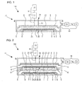
- FIG. 1 shows an entire structure thereof.
- a plasma processing device 100 for manufacturing a thin film according to the first embodiment includes a chamber 15, a gas introducing portion 28 for introducing a reactant gas into the chamber 15, an exhaust unit 29 for discharging the reactant gas in the chamber 15, and a high-frequency power supply unit 30 for applying high-frequency power into the chamber 15.
- the cathode electrode 12 includes a shower plate 2 and a rear plate 3 and is provided so as to face the anode electrode 4.
- a planar shape of the chamber 15 is rectangular, and the chamber 15 includes a main body portion 9 and a door portion 8. Both the main body portion 9 and the door portion 8 can be formed from stainless steel, aluminum alloy, or the like. A joint section of the main body portion 9 and the door portion 8 is sealed with an O-ring (not shown) and the like.
- the chamber 15 is connected with an exhaust unit 29 including an exhaust tube 20, a vacuum pump 21, and a pressure controller 22 so that a degree of vacuum inside the chamber 15 can be arbitrarily controlled.
- Dimensions of the anode electrode 4 are set to appropriate dimensions in accordance with dimensions of a substrate 1 on which the film is to be formed.
- planar dimensions of the substrate 1 are set in a range of 900 x 550 mm to 1200 x 750 mm, while planar dimensions of the anode electrode 4 are accordingly set in a range of 1000 x 600 mm to 1200 x 800 mm, and a thickness thereof is set in a range of 10 to 50 mm.
- the anode electrode 4 can be formed from stainless steel, aluminum alloy, carbon, or the like. In the first embodiment, aluminum alloy is used.
- the anode electrode 4 has a hollow structure, and a heater (sheathed heater) 24 is contained in the hollow section.
- a heater sheathed heater
- the anode electrode 4 is subjected to an annealing process before use so that the processing distortions are eliminated.
- a closed temperature sensor such as a thermocouple 25, is used.
- a processing temperature is different depending on the type of metal used for the anode electrode 4. In the case where aluminum alloy is used, a temperature cycle, in which the anode electrode 4 is maintained at 345°C and then slowly cooled down, is generally adopted.
- the anode electrode 4 is not fixed with a screw or the like but is merely placed on the first supporting members 6. Accordingly, the anode electrode 4, even when heated and expanded, can slide on the first supporting members 6 by the amount of the expansion, which releases the amount of the expansion. As a result, the anode electrode 4 can be freely deflected downward under its own weight.
- the anode electrode 4 and the chamber 15 are electrically connected to each other via four grounding plates.
- Aluminum plates having a width of 10 to 35 mm and a thickness of 0.5 to 3 mm are used as the grounding plates, which are attached to the four corners of the anode electrode 4.
- the cathode electrode 12 is a hollow electrode including the shower plate 2 and the rear plate 3. Both the shower plate 2 and the rear plate 3 can be formed from stainless steel, aluminum alloy, or the like, and are preferably formed from the same material as that of the anode electrode 4. In the first embodiment, aluminum alloy is used.
- Dimensions of the cathode electrode 12 are set to appropriate dimensions in accordance with the dimensions of the substrate 1 on which a film is to be formed.
- planar dimensions of the cathode electrode 12 are set in a range of 1000 x 600 mm to 1200 x 800 mm, and a thickness thereof is set in a range of 10 to 50 mm so as to have the same dimensions as those of the anode electrode 4.
- the inside of the cathode electrode 12 is hollow, and the cathode electrode 12 is connected to the gas introducing portion 28 via a reactant gas tube 23.
- the reactant gas introduced into the cathode electrode 12 from the gas introducing portion 28 via the reactant gas tube 23 is discharged in the form of shower from a plurality of holes formed in the shower plate 2 of the cathode electrode 12.
- the cathode electrode 12 is not fixed with a screw or the like but the shower plate 2 thereof is merely placed on the second supporting members 5. Accordingly, the cathode electrode 12, even when heated and expanded, can slide on the second supporting members 5 by the amount of the expansion, thereby releasing the amount of the expansion. As a result, the cathode electrode 12 can be freely deflected downward under its own weight.
- a tolerance (distance accuracy) of the distance between the anode electrode 4 and the cathode electrode 12 facing each other is desirably within a few percent of the set value.
- the tolerance is thus set because, though there are some changes depending on conditions for the film formation, at least ⁇ 10% of irregularity in the film thickness or a region where the film cannot be formed is generated when the tolerance of the distance between the anode electrode 4 and the cathode electrode 12 facing each other is 4% or more of the set value.
- the tolerance of the distance therebetween is set within 1% in the first embodiment.
- the high-frequency power supply unit 30 including a plasma exciting power supply 10 and an impedance matching device 11 is connected to the cathode electrode 12 via a power introducing terminal 27, so that high-frequency power is applied thereto from the high-frequency power supply unit 30.
- the plasma exciting power supply 10 uses power of 10 W to 100 kW at a frequency of DC to 108.48 MHz. In the first embodiment, power of 10 W to 100 kW at a frequency of 13.56 MHz to 54.24 MHz is used.
- a reactant gas of SiH 4 diluted with H 2 is introduced thereinto based on a predetermined flow rate and pressure via the cathode electrode 12, and the high-frequency power is applied between the cathode electrode 4 and the anode electrode 4 so that the glow discharge is generated.
- a silicon thin film having the film thickness of 300 nm is deposited on the surface of the substrate 1 in the deposition time of ten minutes, with film thickness distribution of ⁇ 10% or less.
- the first-stage cathode electrode 12 (supported by the first-stage second supporting member 5) is provided above the first-stage anode electrode 4 supported by the first-stage first supporting member 6.
- the second-stage first supporting member 6 for supporting the second-stage anode electrode 4 is provided above the first-stage cathode electrode 12.
- the plasma processing device 200 has the two-stage structure, however, may have a structure having at least three stages wherein a similar constitution is repeatedly provided.
- the components such as the chamber 15, gas introducing portion 28, exhaust unit 29, high-frequency power supply unit 30, anode and cathode electrodes 4 and 12, and first and second supporting members 6 and 5, are constituted in substantively the same manner as described in the first embodiment.
Abstract
There is provided a plasma processing device capable of forming a film in a favorable manner irrespective of deflection generated in an anode electrode and a cathode electrode in the case where an area of the electrodes is increased.
A plasma processing device 100 includes a chamber 15, a gas introducing portion 28, an exhaust unit 29, and a high-frequency power supply unit 30. In the chamber 15, there are provided an anode electrode (first electrode) 4 having a flat-plate shape, a cathode electrode (second electrode) 12 having a flat-plate shape, and first supporting members 6 and second supporting members 5 for slidably supporting the two electrodes 4 and 12 in parallel with each other. The cathode electrode 12 is provided so as to face the anode electrode 4. The anode electrode 4 and the cathode electrode 12 are not fixed with screws or the like but are merely placed on the first supporting members 6 and the second supporting members 5. In the anode electrode 4 and the cathode electrode 12, deflection amounts when they are freely deflected under their own weights are equal to each other, and maximum deflection amounts of the two electrodes 4 and 12 are also equal to each other.
Description
- The present invention relates to a plasma processing device for manufacturing a semiconductor thin film and a method for plasma processing using the same, more particularly to a plasma processing device which uses a reaction chamber into which a reactant gas is introduced and a method for plasma processing using the same.
- Conventionally, as a plasma processing device of the foregoing type, there is known a device capable of improving the uniformity in an etching or vapor deposition process in the plasma chemical technology (for example, see the Patent Document 1).
- Patent Document 1: Specification of
U.S. Patent No. 4,264,393 - A plasma CVD device used for manufacturing a semiconductor thin film is generally provided with a cathode and an anode which are provided and supported as a pair, a device for applying high-frequency power to one of the cathode and the anode each having a flat-plate shape, and a device for supplying a reactant gas for the formation of the thin film. In the plasma CVD device, plasma is generated in such a manner that high-frequency power is applied while the reactant gas is supplied between the cathode and the anode. As a result, a thin film is generated on a surface of a substrate provided between the cathode and the anode.
- A distance between the cathode and the anode is referred to as an inter-electrode distance. The inter-electrode distance includes a certain range where plasma can be effectively generated. In the range, the inter-electrode distance is controlled, and the distance is desirably controlled as accurately as possible. The inter-electrode distance is generally controlled with accuracy in the order of 1/100 relative to the inter-electrode distance, in other words, with accuracy of approximately 1% of the inter-electrode distance. In a method of controlling the inter-electrode distance, a sufficient level of rigidity of the cathode and the anode, which are electrodes, is secured relative to their sizes, so that any deflection is not generated in the provided cathode and anode.
- However, the conventional technology has a problem that sufficient rigidity of the electrodes is not obtained in the case where the electrodes are larger and the substrate is accordingly increased in size, which makes it impossible to secure desired accuracy for the inter-electrode distance. As a result, a film cannot be formed in a favorable manner in the plasma processing. In order to secure the desired accuracy in the inter-electrode distance, it may be possible to further increase the rigidity of the electrode, in which case, however, the plasma CVD device is inevitably increased in size as the thicknesses of the electrode are increased and an electrode supporting section is accordingly increased in size.
- Therefore, a main object of the present invention is to provide a plasma processing device capable of forming a film in a favorable manner irrespective of any deflection generated in an anode and a cathode, which are electrodes having a flat-plate shape, in the case where an area of the electrodes is increased.
- According to one aspect of the present invention, there is provided a plasma processing device including a reaction chamber, a gas introducing portion for introducing a reactant gas into the reaction chamber, an exhaust unit for discharging the reactant gas from the reaction chamber, a first electrode and a second electrode supported in the reaction chamber and having a flat-plate shape, and a first supporting member and a second supporting member for supporting the first and second electrodes such that the electrodes face each other, wherein maximum deflection amounts of the first and second electrodes, which are maximum sinking distances thereof under their own weights, in a state where the first and second electrodes are supported by the first and second supporting members, are adapted to be equal to each other.
- With the plasma processing device according to the present invention, a semiconductor thin film uniformly formed on a surface of a substrate having a large area can be obtained with a simplified structure irrespective of any deflection generated in first and second electrodes having a flat-plate shape in the case where an area of the electrodes is increased.
-
-
Fig. 1 is an illustration of an entire structure of a plasma processing device (thin film manufacturing device) according to a first embodiment of the present invention. -
Fig. 2 is an illustration of an entire structure of a plasma processing device (thin film manufacturing device) according to a second embodiment of the present invention. -
- 1 substrate
- 2 shower plate
- 3 rear plate
- 4 anode electrode
- 5 second supporting member
- 6 first supporting member
- 7 tray
- 8 door portion
- 9 main body portion
- 10 plasma exciting power supply
- 11 impedance matching device
- 12 cathode electrode
- 20 exhaust tube
- 21 vacuum pump
- 22 pressure controller
- 23 reactant gas tube
- 24 heater
- 25 thermocouple
- 26 ground wire
- 27 power introducing terminal
- 28 gas introducing portion
- 29 exhaust unit
- 30 high-frequency power supply unit
- In a plasma processing device according to the present invention, shapes, sizes, and materials of first and second electrodes are adapted to be the same, for example, so that a maximum deflection amount of the first electrode, which is a maximum sinking distance thereof under its own weight, and a maximum deflection amount of the second electrode, which is a maximum sinking distance thereof under its own weight, are equal to each other. In this description (including the claims), the recitation "shapes, sizes, materials of first and second electrodes are adapted to be the same" means that there is not any substantive difference mainly between planar shapes, planar dimensions, thicknesses, and basic materials of the two electrodes from the viewpoint of the formation of a semiconductor thin film having desired characteristics on a surface of a substrate. "The maximum deflection amounts of the first and second electrodes are equal to each other" means that there is not any substantive difference between the maximum deflection amounts, which are the maximum sinking distances, when the two electrodes which are placed in a predetermined state are deflected under their own weights in accordance with the rigidity thereof and thereby sink by a certain distance, from the viewpoint of the formation of the semiconductor thin film having desired characteristics on the substrate surface.
- The first and second electrodes may have a hollow structure. In that case, a flow path for the reactant gas or a heater for heating the electrodes may be provided in the respective hollow parts.
- The first and second electrodes may be supported in, for example, peripheral portions thereof to be thereby movable in a limited range. Accordingly, the first and second electrodes can be freely deflected under their own weights, as a result of which the maximum deflection amounts of the two electrodes are equal to each other based on the constitutional characteristics described earlier.
- A metal plate such as stainless steel or aluminum alloy may be used for the first and second electrodes. When these metal plates are annealed at a predetermined annealing temperature, remaining distortions in the metal plates due to a machining process or the like are eliminated, and the same maximum deflection amount can be thereby obtained in the two electrodes.
- The maximum deflection amount, which is the maximum sinking distance, at the time is preferably at least 1% of an inter-electrode distance (distance between the first and second electrodes) because it would be difficult to place the two electrodes so that the maximum deflection amounts of the two electrodes can be equal to each other after they are compared to each other, when the maximum deflection amount fails to reach 1% of the inter-electrode distance. A substrate on which a film is formed through the plasma processing is deflected along the deflection of the first and second electrodes, and then, the thin film is formed thereon. A glass substrate or the like is used as the substrate.
- In order to facilitate handling of the substrate, a film may be formed through the plasma processing in such a manner that a substrate formed from a material such as glass is placed on a tray having a thin-plate shape and formed from aluminum alloy or the like, and the substrate and the tray are deflected along the deflection of the first and second electrodes.
- The plasma processing device according to the present invention is used when a silicon-based thin film is manufactured by the plasma CVD method, for example.
- Examples of the silicon-based thin film include crystalline and amorphous thin films containing silicon as a main component. An example of the reactant gas is a gas containing a silicon element. More specifically, silane (SiH4), disilane (Si2H6), or the like, can be used as the reactant gas, and the silane or disilane may be diluted with hydrogen (H2) or helium (He).
- Other examples of the silicon-based thin film manufactured by the plasma processing device according to the present invention include silicon carbide (SiC) film, silicon nitride (SiN) film, silicon oxide (SiO) film, SiGe film, and the like.
- In order to manufacture a silicon carbide film, a gas containing a carbon element such as CH4 or C2H6 is introduced as the reactant gas at the same time as the introduction of the gas containing the silicon element. In order to manufacture a silicon nitride film, a gas containing a nitrogen element such as NH3 or NO is introduced as the reactant gas at the same time as the introduction of the gas containing the silicon element. In order to manufacture a silicon oxide film, a gas containing an oxygen element such as NO or CO2 is introduced as the reactant gas at the same time as the introduction of the gas containing the silicon element. In order to manufacture a SiGe film, a gas containing a germanium element such as GeH4 is introduced as the reactant gas at the same time as the introduction of the gas containing the silicon element.
- Further, impurities may be doped into the silicon-based thin film in order to control conductivity. In that case, a gas containing impurities such as PH3 is simultaneously introduced for the n-type, while a gas containing impurities such as B2H6 is simultaneously introduced for the p-type.
- An example of the reaction chamber in the plasma processing device according to the present invention is a chamber capable of exhausting at least the inside thereof to be vacuum. Such a reaction chamber can be formed from, for example, stainless steel, aluminum alloy, or the like. In the case where at least two different members constitute the reaction chamber, the reaction chamber is preferably provided with an O-ring, or the like at their joint section to be completely sealed.
- As the gas introducing portion in the plasma processing device according to the present invention can be used, for example, ones commonly used in the plasma CVD device; however, the gas introducing portion is not necessarily limited thereto.
- For example, a vacuum pump, an exhaust tube which connects the reaction chamber to the vacuum pump, and a pressure controller provided at an intermediate position in the exhaust tube may constitute the exhaust unit in the plasma processing device according to the present invention.
- In the plasma processing device according to the present invention, a high-frequency power supply unit for applying high-frequency power between the first and second electrodes is provided. For example, a plasma exciting power supply, an impedance matching device, and the like may constitute the high-frequency power supply unit.
- In the plasma processing device according to the present invention, the first and second electrodes may be formed from a heat-resistant conductive material having a flat-plate shape such as stainless steel, aluminum alloy, carbon, or the like. It is preferable that the shapes, sizes, and materials of the first and second electrodes be the same. Further, in the case where there are remaining processing distortions resulting from the machining process or the like, it is preferable to eliminate them in an annealing process.
- The first electrode may be an anode electrode having a hollow structure and provided with a heater therein, and the second electrode may be a cathode electrode having a hollow structure and provided with a large number of holes on a surface thereof facing the first electrode.
- In the plasma processing device according to the present invention, first and second supporting members may support the first and second electrodes so that the first and second electrodes are orthogonal to the direction of gravitational force, in other words, so that they are horizontally supported. In the case where the first and second electrodes are substantially square, for example, in the foregoing constitution, four divided supporting pieces which support four corners of the first and second electrodes may constitute the first and second supporting members.
- In the case where the four divided supporting pieces constitute the first and second supporting members, the four divided supporting pieces constituting the second supporting member may be fixed to upper ends of four support pillars extending vertically upward from a bottom surface of the reaction chamber.
- The shapes and the constitutions of the first and second supporting members are not necessarily limited to those described above. The first and second supporting members may be, e.g., two pedestals having a frame shape which respectively support only edges of the first and second electrodes. Further, the two pedestals having the frame shape may be vertically coupled with each other to be integrally formed.
- Thus, the shapes and the constitutions of the first and second supporting members are not subject to any particular limitation as far as they can support the first and second electrodes in parallel with each other and support at least one of the first and second electrodes in a slidable manner.
- In the plasma processing device according to the present invention, both the first and second supporting members include engagement protrusions, the engagement protrusions loosely engaging to edges of the first and second electrodes. The engagement protrusions may be provided so that gaps are generated between the edges of the first and second electrodes and the respective engagement protrusions.
- In the case where the four divided supporting pieces constitute the first and second supporting members as described above, each of the four divided supporting pieces may be provided with an engagement protrusion. In the case where the two pedestals having the frame shape constitute the first and second supporting members as described above, the respective engagement protrusions may be protruded along outer peripheries of the pedestals.
- The first and second supporting members may be formed from an insulating material. An example of the insulating material constituting the first and second supporting members may be a heat-resistant material superior in insulating and thermal insulating properties such as glass, alumina, or zirconia. In the case where one of the first and second electrodes is provided, a conductor may be used in the supporting member on the side of the provided electrode.
- A plurality of pairs of first and second electrodes and a plurality of pairs of first and second supporting members may be provided in one reaction chamber.
- The first and second electrodes are freely deflected in the direction of gravitational force according to the supporting method described above. An amount of the free deflection, which is the sinking distance, is preferably at least 1% of the distance of the distance between the first and second electrodes (inter-electrode distance) as described above.
- A substrate on which the thin film is formed is provided between the first and second electrodes, and the substrate is adapted to be very thin and deflected along the deflection of the first and second electrodes. A glass substrate, on a surface of which a transparent conductive film is applied, is a candidate for the substrate. The substrate may be set on a
tray 7 formed from the same material as that of the first and second electrodes and then handled so that the substrate can be easily transported. Thetray 7 has planar dimensions equal to or slightly larger than those of the substrate. - According to another aspect of the present invention, a plasma processing method is provided by means of the plasma processing device according to one aspect described above. In the plasma processing method, a substrate on which a thin film is to be formed is deflected along the deflection of first and second electrodes and provided between the two electrodes, a reactant gas is supplied into a reaction chamber, and high-frequency power is applied between the first and second electrodes so that a semiconductor thin film is formed on a surface of the substrate.
- Preferred embodiments of the plasma processing device according to the present invention are described in detail below referring to the drawings. In the preferred embodiments described below, members commonly used are denoted by the same reference numerals.
- A plasma processing device for manufacturing a thin film according to a first embodiment of the present invention is described referring to
Fig. 1 which shows an entire structure thereof. - As shown in
Fig. 1 , aplasma processing device 100 for manufacturing a thin film according to the first embodiment includes achamber 15, agas introducing portion 28 for introducing a reactant gas into thechamber 15, anexhaust unit 29 for discharging the reactant gas in thechamber 15, and a high-frequencypower supply unit 30 for applying high-frequency power into thechamber 15. - In the
chamber 15, there are provided a rectangular anode electrode (first electrode) 4 having a flat-plate shape, a rectangular cathode electrode (second electrode) 12 having a flat-plate shape, and first supportingmembers 6 and second supportingmembers 5 for slidably supporting the twoelectrodes cathode electrode 12 includes ashower plate 2 and arear plate 3 and is provided so as to face theanode electrode 4. - A planar shape of the
chamber 15 is rectangular, and thechamber 15 includes a main body portion 9 and adoor portion 8. Both the main body portion 9 and thedoor portion 8 can be formed from stainless steel, aluminum alloy, or the like. A joint section of the main body portion 9 and thedoor portion 8 is sealed with an O-ring (not shown) and the like. - The
chamber 15 is connected with anexhaust unit 29 including anexhaust tube 20, avacuum pump 21, and apressure controller 22 so that a degree of vacuum inside thechamber 15 can be arbitrarily controlled. - On a rectangular bottom surface of the main body portion 9 of the
chamber 15, each of the first supportingmembers 6 is provided in the vicinity of each corner of the bottom surface, and theanode electrode 4 is placed on these first supportingmembers 6. Based on a reason described later, four divided supporting pieces each having a small block shape constitute the first supportingmembers 6, and the four corners of theanode electrode 4 are supported by these four divided supporting pieces. - Dimensions of the
anode electrode 4 are set to appropriate dimensions in accordance with dimensions of a substrate 1 on which the film is to be formed. In the first embodiment, planar dimensions of the substrate 1 are set in a range of 900 x 550 mm to 1200 x 750 mm, while planar dimensions of theanode electrode 4 are accordingly set in a range of 1000 x 600 mm to 1200 x 800 mm, and a thickness thereof is set in a range of 10 to 50 mm. - The
anode electrode 4 can be formed from stainless steel, aluminum alloy, carbon, or the like. In the first embodiment, aluminum alloy is used. - The
anode electrode 4 has a hollow structure, and a heater (sheathed heater) 24 is contained in the hollow section. In theanode electrode 4, there remain processing distortions resulting from a machining process adopted for the formation of the hollow structure. Therefore, theanode electrode 4 is subjected to an annealing process before use so that the processing distortions are eliminated. In the annealing process, a closed temperature sensor, such as athermocouple 25, is used. In the annealing process, a processing temperature is different depending on the type of metal used for theanode electrode 4. In the case where aluminum alloy is used, a temperature cycle, in which theanode electrode 4 is maintained at 345°C and then slowly cooled down, is generally adopted. - The
anode electrode 4 is not fixed with a screw or the like but is merely placed on the first supportingmembers 6. Accordingly, theanode electrode 4, even when heated and expanded, can slide on the first supportingmembers 6 by the amount of the expansion, which releases the amount of the expansion. As a result, theanode electrode 4 can be freely deflected downward under its own weight. - The
anode electrode 4 and thechamber 15 are electrically connected to each other via four grounding plates. Aluminum plates having a width of 10 to 35 mm and a thickness of 0.5 to 3 mm are used as the grounding plates, which are attached to the four corners of theanode electrode 4. - The
cathode electrode 12 is a hollow electrode including theshower plate 2 and therear plate 3. Both theshower plate 2 and therear plate 3 can be formed from stainless steel, aluminum alloy, or the like, and are preferably formed from the same material as that of theanode electrode 4. In the first embodiment, aluminum alloy is used. - Dimensions of the
cathode electrode 12 are set to appropriate dimensions in accordance with the dimensions of the substrate 1 on which a film is to be formed. In the first embodiment, planar dimensions of thecathode electrode 12 are set in a range of 1000 x 600 mm to 1200 x 800 mm, and a thickness thereof is set in a range of 10 to 50 mm so as to have the same dimensions as those of theanode electrode 4. - The inside of the
cathode electrode 12 is hollow, and thecathode electrode 12 is connected to thegas introducing portion 28 via areactant gas tube 23. The reactant gas introduced into thecathode electrode 12 from thegas introducing portion 28 via thereactant gas tube 23 is discharged in the form of shower from a plurality of holes formed in theshower plate 2 of thecathode electrode 12. - Each of the plurality of holes in the
shower plate 2 preferably has a diameter of 0.1 to 2.0 mm, and the holes are desirably formed so that an interval between the adjacent holes is of a pitch of a few millimeters to a few centimeters. - There remain processing distortions due to the machining process in
shower plate 2 of thecathode electrode 12. Therefore, theshower plate 12 is subjected to the annealing process before use so that the processing distortions can be eliminated therefrom. A processing temperature in the annealing process is different depending on the type of metal used for thecathode electrode 12 and theshower plate 2. In the case where aluminum alloy is used for these components, a temperature cycle, in which these components are maintained at 345°C and then slowly cooled down, is generally adopted. - The
shower plate 2 in thecathode electrode 12 is placed on the total of four second supportingmembers 5, each of which being provided at each of the four corners distant upward from the bottom surface of the main body portion 9 of thechamber 15. The second supportingmembers 5 can be formed from glass, alumina, zirconia, or the like. In the first embodiment, alumina or zirconia is used. - The
cathode electrode 12 is not fixed with a screw or the like but theshower plate 2 thereof is merely placed on the second supportingmembers 5. Accordingly, thecathode electrode 12, even when heated and expanded, can slide on the second supportingmembers 5 by the amount of the expansion, thereby releasing the amount of the expansion. As a result, thecathode electrode 12 can be freely deflected downward under its own weight. - The deflection amounts of the
anode electrode 4 and thecathode electrode 12 when they are freely deflected under their own weights, which are the sinking distances thereof, are equal to each other, and maximum deflection amounts of the twoelectrodes cathode electrode 12, in which the length of the long side is approximately 1000 mm, the length of the short side is approximately 600 mm, and the thickness is 15 mm, the maximum deflection amount of thecathode electrode 12 is approximately 1.2 mm. This value is 12% of 10 mm, which is a set distance between theanode electrode 4 and the cathode electrode 12 (inter-electrode distance) used in the first embodiment. - A tolerance (distance accuracy) of the distance between the
anode electrode 4 and thecathode electrode 12 facing each other is desirably within a few percent of the set value. The tolerance is thus set because, though there are some changes depending on conditions for the film formation, at least ±10% of irregularity in the film thickness or a region where the film cannot be formed is generated when the tolerance of the distance between theanode electrode 4 and thecathode electrode 12 facing each other is 4% or more of the set value. The tolerance of the distance therebetween is set within 1% in the first embodiment. - In the first embodiment, the square glass substrate 1 having the lengths of approximately 1000mm x approximately 1000 mm and the thickness of approximately 2 mm is used, and the glass substrate 1 is placed on the
square tray 7 having the same dimensions and the thickness of 1.0 mm and formed from aluminum alloy and then set on theanode electrode 4 to be thereby easily moved. In comparison to theanode electrode 4, the glass substrate 1 and thetray 7 are sufficiently thin, light, and less rigid. Therefore, when the glass substrate 1 and thetray 7 are set along the deflection of theanode electrode 4, the deflection of theanode electrode 4 is hardly increased. - The high-frequency
power supply unit 30 including a plasmaexciting power supply 10 and animpedance matching device 11 is connected to thecathode electrode 12 via apower introducing terminal 27, so that high-frequency power is applied thereto from the high-frequencypower supply unit 30. The plasmaexciting power supply 10 uses power of 10 W to 100 kW at a frequency of DC to 108.48 MHz. In the first embodiment, power of 10 W to 100 kW at a frequency of 13.56 MHz to 54.24 MHz is used. - In the thin
film manufacturing device 100 according to the first embodiment constituted as above, a reactant gas of SiH4 diluted with H2 is introduced thereinto based on a predetermined flow rate and pressure via thecathode electrode 12, and the high-frequency power is applied between thecathode electrode 4 and theanode electrode 4 so that the glow discharge is generated. As a result, a silicon thin film having the film thickness of 300 nm is deposited on the surface of the substrate 1 in the deposition time of ten minutes, with film thickness distribution of ± 10% or less. - A plasma processing device for manufacturing a thin film according to a second embodiment is described referring to
Fig. 2 . Aplasma processing device 200 according to the second embodiment has a two-stage structure including two pairs ofanode electrodes 4 andcathode electrodes 12 and two pairs of first and second supportingmembers - More specifically, the first-stage cathode electrode 12 (supported by the first-stage second supporting member 5) is provided above the first-
stage anode electrode 4 supported by the first-stage first supportingmember 6. The second-stage first supportingmember 6 for supporting the second-stage anode electrode 4 is provided above the first-stage cathode electrode 12. With such a two-stage structure, the two pairs of anode andcathode electrodes - In the second embodiment, the
plasma processing device 200 has the two-stage structure, however, may have a structure having at least three stages wherein a similar constitution is repeatedly provided. - The components, such as the
chamber 15,gas introducing portion 28,exhaust unit 29, high-frequencypower supply unit 30, anode andcathode electrodes members
Claims (12)
- A plasma processing device comprising:a reaction chamber;a gas introducing portion that introduces a reactant gas into the reaction chamber;an exhaust unit that discharges the reactant gas from the reaction chamber;a first electrode and a second electrode supported in the reaction chamber and having a flat-plate shape; anda first supporting member and a second supporting member that support the first and second electrodes such that the electrodes face each other, whereinmaximum deflection amounts of the first and second electrodes, which are maximum sinking distances under their own weights, in a state where the first and second electrodes are supported by the first and second supporting members, are adapted to be equal to each other.
- The plasma processing device according to claim 1, wherein
shapes, sizes, and materials of the first and second electrodes are adapted to be the same. - The plasma processing device according to claim 1 or 2, wherein the first and second electrodes have a hollow structure.
- The plasma processing device according to any one of claims 1 to 3, wherein the first and second electrodes are supported to be movable in a limited range.
- The plasma processing device according to claim 2, wherein a material used for the first and second electrodes is aluminum alloy.
- The plasma processing device according to any one of claims 1 to 4, wherein the first and second electrodes are subjected to an annealing process.
- The plasma processing device according to any one of claims 1 to 4, wherein
the first and second electrodes are distant from each other by a predetermined inter-electrode distance,
the sizes, the shapes, and the materials of the first and second electrodes are adapted in such a manner that maximum deflection amounts thereof are at least 1% of the inter-electrode distance, and
the first and second electrodes are supported by the first and second supporting members. - A method for plasma processing, wherein the plasma processing device according to any one of claims 1 to 7 is used, and
a substrate to be processed is deflected along the deflection of the first and second electrodes and provided between the two electrodes, and a semiconductor thin film is thereby formed on a surface of the substrate. - The method for plasma processing according to claim 8, wherein
a glass substrate is set on one of the first and second electrodes. - The plasma processing device according to claim 1, wherein
a substrate to be processed is provided between the first and second electrodes in a state where the substrate is deflected along the deflection of the two electrodes. - The plasma processing device according to claim 10, further comprising a tray having a thin-plate shape on which the substrate is placed.
- The plasma processing device according to claim 11, wherein the substrate is set on the tray.
Applications Claiming Priority (2)
| Application Number | Priority Date | Filing Date | Title |
|---|---|---|---|
| JP2005340847 | 2005-11-25 | ||
| PCT/JP2006/322844 WO2007060876A1 (en) | 2005-11-25 | 2006-11-16 | Plasma processing apparatus and plasma processing method |
Publications (2)
| Publication Number | Publication Date |
|---|---|
| EP1959480A1 true EP1959480A1 (en) | 2008-08-20 |
| EP1959480A4 EP1959480A4 (en) | 2010-04-21 |
Family
ID=38067107
Family Applications (1)
| Application Number | Title | Priority Date | Filing Date |
|---|---|---|---|
| EP06832733A Withdrawn EP1959480A4 (en) | 2005-11-25 | 2006-11-16 | Plasma processing apparatus and plasma processing method |
Country Status (7)
| Country | Link |
|---|---|
| US (1) | US8093142B2 (en) |
| EP (1) | EP1959480A4 (en) |
| JP (1) | JP4728345B2 (en) |
| KR (1) | KR101080437B1 (en) |
| CN (1) | CN101336467B (en) |
| TW (1) | TW200732505A (en) |
| WO (1) | WO2007060876A1 (en) |
Families Citing this family (6)
| Publication number | Priority date | Publication date | Assignee | Title |
|---|---|---|---|---|
| US7727588B2 (en) * | 2003-09-05 | 2010-06-01 | Yield Engineering Systems, Inc. | Apparatus for the efficient coating of substrates |
| CN101296554B (en) * | 2008-06-19 | 2011-01-26 | 友达光电股份有限公司 | Plasma processing device and electric pole plate thereof |
| TW201101937A (en) * | 2010-06-23 | 2011-01-01 | Linco Technology Co Ltd | High-density electrode device for plasma surface treatment |
| TWI489517B (en) * | 2013-05-07 | 2015-06-21 | Univ Nat Taiwan | Apparatus of surface finishing and the method thereof |
| CN104822219B (en) * | 2015-05-18 | 2017-09-19 | 京东方科技集团股份有限公司 | Plasma generator, annealing device, plated film crystallization equipment and annealing process |
| DE102018103949A1 (en) | 2018-02-21 | 2019-08-22 | Christof-Herbert Diener | Low-pressure plasma chamber, low-pressure plasma system and method for producing a low-pressure plasma chamber |
Citations (4)
| Publication number | Priority date | Publication date | Assignee | Title |
|---|---|---|---|---|
| US4148705A (en) * | 1976-03-03 | 1979-04-10 | Dionex Corporation | Gas plasma reactor and process |
| US4264393A (en) * | 1977-10-31 | 1981-04-28 | Motorola, Inc. | Reactor apparatus for plasma etching or deposition |
| EP1420081A2 (en) * | 2002-10-11 | 2004-05-19 | Sharp Kabushiki Kaisha | Thin film formation apparatus and thin film formation method employing the apparatus |
| JP2004149917A (en) * | 2002-10-11 | 2004-05-27 | Sharp Corp | Thin film production apparatus, and thin film production method using the apparatus |
Family Cites Families (12)
| Publication number | Priority date | Publication date | Assignee | Title |
|---|---|---|---|---|
| DE2758569A1 (en) | 1977-12-29 | 1979-07-05 | Bayer Ag | HYDANTOINE |
| JPH0314228A (en) * | 1989-06-13 | 1991-01-22 | Nec Corp | Plasma process device |
| US5074456A (en) * | 1990-09-18 | 1991-12-24 | Lam Research Corporation | Composite electrode for plasma processes |
| JP3884561B2 (en) * | 1998-04-10 | 2007-02-21 | サムコ株式会社 | Plasma cleaning device |
| US6073577A (en) * | 1998-06-30 | 2000-06-13 | Lam Research Corporation | Electrode for plasma processes and method for manufacture and use thereof |
| JP2005260251A (en) * | 1999-04-06 | 2005-09-22 | Tokyo Electron Ltd | Mounting stand, plasma processing apparatus, and manufacturing method for mounting stand |
| US6461444B1 (en) * | 1999-08-20 | 2002-10-08 | Kaneka Corporation | Method and apparatus for manufacturing semiconductor device |
| JP4856308B2 (en) * | 2000-12-27 | 2012-01-18 | キヤノンアネルバ株式会社 | Substrate processing apparatus and via chamber |
| US20040173313A1 (en) * | 2003-03-03 | 2004-09-09 | Bradley Beach | Fire polished showerhead electrode |
| US7083702B2 (en) | 2003-06-12 | 2006-08-01 | Applied Materials, Inc. | RF current return path for a large area substrate plasma reactor |
| JP3709413B1 (en) * | 2003-06-25 | 2005-10-26 | 積水化学工業株式会社 | Surface treatment apparatus and method |
| JP2006086470A (en) * | 2004-09-17 | 2006-03-30 | Sharp Corp | Plasma generator |
-
2006
- 2006-11-16 CN CN2006800518014A patent/CN101336467B/en not_active Expired - Fee Related
- 2006-11-16 JP JP2007546414A patent/JP4728345B2/en not_active Expired - Fee Related
- 2006-11-16 EP EP06832733A patent/EP1959480A4/en not_active Withdrawn
- 2006-11-16 US US12/094,816 patent/US8093142B2/en not_active Expired - Fee Related
- 2006-11-16 WO PCT/JP2006/322844 patent/WO2007060876A1/en active Application Filing
- 2006-11-16 KR KR1020087015329A patent/KR101080437B1/en not_active IP Right Cessation
- 2006-11-24 TW TW095143613A patent/TW200732505A/en not_active IP Right Cessation
Patent Citations (4)
| Publication number | Priority date | Publication date | Assignee | Title |
|---|---|---|---|---|
| US4148705A (en) * | 1976-03-03 | 1979-04-10 | Dionex Corporation | Gas plasma reactor and process |
| US4264393A (en) * | 1977-10-31 | 1981-04-28 | Motorola, Inc. | Reactor apparatus for plasma etching or deposition |
| EP1420081A2 (en) * | 2002-10-11 | 2004-05-19 | Sharp Kabushiki Kaisha | Thin film formation apparatus and thin film formation method employing the apparatus |
| JP2004149917A (en) * | 2002-10-11 | 2004-05-27 | Sharp Corp | Thin film production apparatus, and thin film production method using the apparatus |
Non-Patent Citations (1)
| Title |
|---|
| See also references of WO2007060876A1 * |
Also Published As
| Publication number | Publication date |
|---|---|
| JPWO2007060876A1 (en) | 2009-05-07 |
| TW200732505A (en) | 2007-09-01 |
| US20090253246A1 (en) | 2009-10-08 |
| JP4728345B2 (en) | 2011-07-20 |
| EP1959480A4 (en) | 2010-04-21 |
| KR101080437B1 (en) | 2011-11-04 |
| WO2007060876A1 (en) | 2007-05-31 |
| US8093142B2 (en) | 2012-01-10 |
| CN101336467B (en) | 2010-05-26 |
| CN101336467A (en) | 2008-12-31 |
| TWI333510B (en) | 2010-11-21 |
| KR20080070771A (en) | 2008-07-30 |
Similar Documents
| Publication | Publication Date | Title |
|---|---|---|
| KR101593460B1 (en) | Ground return for plasma processes | |
| TWI449121B (en) | Substrate support regulating temperature of substrate and uses thereof | |
| US8093142B2 (en) | Plasma processing apparatus and plasma processing method | |
| TWI744229B (en) | Wafer boat, treatment apparatus for wafers and treatment method for wafers | |
| US7927455B2 (en) | Plasma processing apparatus | |
| US7032536B2 (en) | Thin film formation apparatus including engagement members for support during thermal expansion | |
| TW201704563A (en) | Wafer boat and treatment apparatus for wafers | |
| CN102376564A (en) | A-si seasoning effect to improve sin run-to-run uniformity | |
| KR101224669B1 (en) | Plasma processing apparatus | |
| JP2616760B2 (en) | Plasma gas phase reactor | |
| US7722738B2 (en) | Semiconductor device manufacturing unit and semiconductor device manufacturing method | |
| KR102146600B1 (en) | Substrate processing apparatus and substrate processing method | |
| JP4936297B2 (en) | Plasma processing apparatus, plasma processing method, and semiconductor device | |
| TW202102066A (en) | Ground strap assemblies | |
| JP4421864B2 (en) | Thin film manufacturing apparatus and thin film manufacturing method using the apparatus | |
| JP4890313B2 (en) | Plasma CVD equipment | |
| JP2012507133A (en) | Deposition apparatus for improving uniformity of material processed on a substrate and method of using the same | |
| JP2004091885A (en) | Apparatus for depositing thin film and method for depositing thin film using this apparatus | |
| EP2299479A1 (en) | Plasma processing apparatus, and film forming method and etching method using plasma processing apparatus | |
| KR20090073272A (en) | Substrate processing method using capacitively coupled electrodes with laser beam | |
| JPH07263364A (en) | Method of plasma vapor-phase reaction |
Legal Events
| Date | Code | Title | Description |
|---|---|---|---|
| PUAI | Public reference made under article 153(3) epc to a published international application that has entered the european phase |
Free format text: ORIGINAL CODE: 0009012 |
|
| 17P | Request for examination filed |
Effective date: 20080611 |
|
| AK | Designated contracting states |
Kind code of ref document: A1 Designated state(s): DE ES GB IT |
|
| RBV | Designated contracting states (corrected) |
Designated state(s): DE ES GB IT |
|
| A4 | Supplementary search report drawn up and despatched |
Effective date: 20100323 |
|
| 17Q | First examination report despatched |
Effective date: 20101013 |
|
| DAX | Request for extension of the european patent (deleted) | ||
| STAA | Information on the status of an ep patent application or granted ep patent |
Free format text: STATUS: THE APPLICATION IS DEEMED TO BE WITHDRAWN |
|
| 18D | Application deemed to be withdrawn |
Effective date: 20150602 |