EP1975587A1 - Pressure sensor package and electronic part - Google Patents
Pressure sensor package and electronic part Download PDFInfo
- Publication number
- EP1975587A1 EP1975587A1 EP07707089A EP07707089A EP1975587A1 EP 1975587 A1 EP1975587 A1 EP 1975587A1 EP 07707089 A EP07707089 A EP 07707089A EP 07707089 A EP07707089 A EP 07707089A EP 1975587 A1 EP1975587 A1 EP 1975587A1
- Authority
- EP
- European Patent Office
- Prior art keywords
- pressure sensor
- section
- sensor package
- semiconductor substrate
- bump
- Prior art date
- Legal status (The legal status is an assumption and is not a legal conclusion. Google has not performed a legal analysis and makes no representation as to the accuracy of the status listed.)
- Withdrawn
Links
Images


Classifications
-
- G—PHYSICS
- G01—MEASURING; TESTING
- G01L—MEASURING FORCE, STRESS, TORQUE, WORK, MECHANICAL POWER, MECHANICAL EFFICIENCY, OR FLUID PRESSURE
- G01L9/00—Measuring steady of quasi-steady pressure of fluid or fluent solid material by electric or magnetic pressure-sensitive elements; Transmitting or indicating the displacement of mechanical pressure-sensitive elements, used to measure the steady or quasi-steady pressure of a fluid or fluent solid material, by electric or magnetic means
- G01L9/0041—Transmitting or indicating the displacement of flexible diaphragms
- G01L9/0042—Constructional details associated with semiconductive diaphragm sensors, e.g. etching, or constructional details of non-semiconductive diaphragms
-
- G—PHYSICS
- G01—MEASURING; TESTING
- G01L—MEASURING FORCE, STRESS, TORQUE, WORK, MECHANICAL POWER, MECHANICAL EFFICIENCY, OR FLUID PRESSURE
- G01L19/00—Details of, or accessories for, apparatus for measuring steady or quasi-steady pressure of a fluent medium insofar as such details or accessories are not special to particular types of pressure gauges
- G01L19/0061—Electrical connection means
- G01L19/0069—Electrical connection means from the sensor to its support
-
- G—PHYSICS
- G01—MEASURING; TESTING
- G01L—MEASURING FORCE, STRESS, TORQUE, WORK, MECHANICAL POWER, MECHANICAL EFFICIENCY, OR FLUID PRESSURE
- G01L9/00—Measuring steady of quasi-steady pressure of fluid or fluent solid material by electric or magnetic pressure-sensitive elements; Transmitting or indicating the displacement of mechanical pressure-sensitive elements, used to measure the steady or quasi-steady pressure of a fluid or fluent solid material, by electric or magnetic means
- G01L9/0041—Transmitting or indicating the displacement of flexible diaphragms
- G01L9/0051—Transmitting or indicating the displacement of flexible diaphragms using variations in ohmic resistance
- G01L9/0052—Transmitting or indicating the displacement of flexible diaphragms using variations in ohmic resistance of piezoresistive elements
- G01L9/0054—Transmitting or indicating the displacement of flexible diaphragms using variations in ohmic resistance of piezoresistive elements integral with a semiconducting diaphragm
-
- H—ELECTRICITY
- H01—ELECTRIC ELEMENTS
- H01L—SEMICONDUCTOR DEVICES NOT COVERED BY CLASS H10
- H01L2224/00—Indexing scheme for arrangements for connecting or disconnecting semiconductor or solid-state bodies and methods related thereto as covered by H01L24/00
- H01L2224/01—Means for bonding being attached to, or being formed on, the surface to be connected, e.g. chip-to-package, die-attach, "first-level" interconnects; Manufacturing methods related thereto
- H01L2224/42—Wire connectors; Manufacturing methods related thereto
- H01L2224/47—Structure, shape, material or disposition of the wire connectors after the connecting process
- H01L2224/48—Structure, shape, material or disposition of the wire connectors after the connecting process of an individual wire connector
- H01L2224/4805—Shape
- H01L2224/4809—Loop shape
- H01L2224/48091—Arched
Landscapes
- Physics & Mathematics (AREA)
- General Physics & Mathematics (AREA)
- Chemical & Material Sciences (AREA)
- Analytical Chemistry (AREA)
- Measuring Fluid Pressure (AREA)
- Pressure Sensors (AREA)
Abstract
A pressure sensor package (10) of the present invention includes: a pressure sensor (11) including at least a first conductive portion (17) having a space (13) inside a central region (α) on a surface of a semiconductor substrate, a thin-plate region above the space serving as a diaphragm section (14), and pressure sensitive elements (15) arranged in the diaphragm section, the first conductive portion being arranged on a peripheral region (β) excluding the diaphragm section on the surface and electrically connected to each of the pressure sensitive elements (15); and a first bump (18) arranged on the first conductive portion and electrically connected to it, wherein the thickness D1 of the semiconductor substrate at the peripheral region, the thickness D2 of the diaphragm section, the height D3 of the space, and the remaining thickness D4 of the semiconductor substrate excluding D2 and D3 at the central region satisfy the relationships: (D2+D3) << D4, and D1 being nearly equal to D4.
Description
- The present invention relates to a pressure sensor package and an electronic part.
This application claims priority on Japanese Patent Application No.2006-10961 filed on January 19, 2006 2006-256003 filed on September 21, 2006 - An exemplary pressure sensor with a semiconductor substrate (hereinafter, referred to as a "semiconductor pressure sensor") is shown in
Fig. 11 . Asemiconductor pressure sensor 100 includes athin diaphragm section 102 and fourgauge resistance elements 103. Thethin diaphragm section 102 is formed by etching from a back surface of asemiconductor substrate 101. Thegauge resistance elements 103 are formed on a front surface of thesemiconductor substrate 101. Thegauge resistance elements 103 are electrically connected to one another so as to form a Wheatstone bridge. When thediaphragm section 102 is bent under pressure, stress in response to the amount of bending of thediaphragm section 102 is applied to eachgauge resistance element 103. The resistance value of thegauge resistance element 103 changes due to the stress. Thesemiconductor pressure sensor 100 detects pressure by detecting and picking up the change in the resistance value as electric signals (seeFig. 5 of Patent Document 1). - The semiconductor pressure sensor is packaged as shown in
Fig. 12 for normal use. Apressure sensor package 200 essentially includes acasing 204 which consists of abase 201 of an insulating material, and aresin cover 203. Thecover 203 includes apressure inlet 202. Inside thecasing 204, a pressure sensor 205 (100) is disposed on thebase 201 and is electrically connected to alead 207 via abonding wire 206. In this structure, the pressure sensor 205 (100), as a component of thepressure sensor package 200, may be connected to an external amplifier circuit or compensating circuit (not shown) via thelead 207. - Patent Document 1: Japanese Unexamined Patent Application No.
2002-340714 - Conventional pressure sensor packages have at least the following two problems.
- (1) In a package having a pressure sensor disposed inside the case, even if the pressure sensor can be made smaller, it is difficult to make the entire package compact unless the casing is also made smaller.
- (2) In order to produce a package having the structure described above, the process requires providing multiple pressure sensors on a semiconductor substrate, cutting the substrate into chips with a pressure sensor, and then packaging each chip. The conventional process requires a large number of processes at a high cost. Thus, it is difficult to manufacture the pressure sensor package at a lower cost.
- In view of the aforementioned, an object of the invention is to provide a compact, low-cost pressure sensor package by devising a wafer level package which serves as a pressure sensor. Another object of the invention is to provide a compact, lightweight electronic part on which the pressure sensor package is mounted.
- A first aspect of the invention is a pressure sensor package which includes: a pressure sensor including at least a first conductive portion having a space inside a central region on a surface of a semiconductor substrate, a thin-plate region above the space being defined as a diaphragm section, and pressure sensitive elements arranged in the diaphragm section, the first conductive portion being arranged on a peripheral region excluding the diaphragm section on the surface and electrically connected to each of the pressure sensitive elements; and a first bump arranged on the first conductive portion and electrically connected to it, wherein the thickness D1 of the semiconductor substrate at the peripheral region, the thickness D2 of the diaphragm section, the height D3 of the space, and the remaining thickness D4 of the semiconductor substrate excluding D2 and D3 at the central region satisfy the relationships: (D2+D3) « D4, and D1 being nearly equal to D4.
- A second aspect of the invention is a pressure sensor package which includes: a pressure sensor including at least a first conductive portion having a space inside a central region on a surface of a semiconductor substrate, a thin-plate region above the space serving as a diaphragm section, and pressure sensitive elements arranged in the diaphragm section, the first conductive portion being arranged on a peripheral region excluding the diaphragm section on the surface and electrically connected to each of the pressure sensitive elements; a first insulating section disposed so as to cover the peripheral region; a second insulating section disposed on the first insulating section and electrically connected to the first conductive section; and a second bump arranged on the second conductive portion and electrically connected to it at a position not overlapping with the first conductive section, wherein the thickness D1 of the semiconductor substrate at the peripheral region, the thickness D2 of the diaphragm section, the height D3 of the space, and the remaining thickness D4 of the semiconductor substrate excluding D2 and D3 at the central region satisfy the relationships: (D2+D3) <<D4, and D 1 being nearly equal to D4.
- A third aspect of the invention further includes, in the second aspect, a second insulating section disposed so as to cover the peripheral region including the second conductive section with only the second bump exposed.
- A fourth aspect of the invention further includes, in the second aspect, a second insulating section disposed to overlap with the first insulating section so as to cover the second conductive section with only the second bump exposed, wherein at least one of the first insulating section and the second insulating section is disposed in the vicinity of an island-shaped second bump.
- A fifth aspect of the invention is characterized in that the second bumps are positioned at positions which are symmetrical with one another, in the second aspect.
- A sixth aspect of the invention further includes, in any one of the first to fifth aspects, an amplifier circuit and/or a compensating circuit inside the pressure sensor.
A seventh aspect of the invention is characterized in that, in the second aspect, the first insulating section is formed in an island shape. - An electronic part according to the invention includes the pressure sensor package of any one of the first to seventh aspect mounted thereon.
- In the pressure sensor package according to the first aspect of the invention (hereinafter, referred to as a "first pressure sensor package"), the pressure sensor itself has the diaphragm section and the first conductive section separately on the same semiconductor substrate. The first conductive section is electrically connected to the pressure sensitive element and has the first bump arranged thereon. The dimensions D2 to D4 at the central region at which the diaphragm section is disposed and the dimension D1 of the peripheral region at which the first conductive section is disposed to satisfy the relationships: (D2+D3) <<D4, and D1 being nearly equal to D4. That is, the first pressure sensor is produced from a semiconductor substrate whose material is the same at the central region having the diaphragm section overlapping therewith and at the peripheral region. The thickness of the semiconductor substrate is substantially the same at the central region and the peripheral region. Such a structure has an advantageous effect to suppress the mechanical or thermal influence exerted on the diaphragm section and the pressure sensitive element when the pressure sensor is connected to an external substrate via the first bump. In addition, such a structure in which the pressure sensor is connected to the external substrate via the first bump eliminates the need of a conventionally-required casing for containing the pressure sensor, or connecting elements such as bonding wires and leads for electrically connecting the pressure sensor and the external substrate. Accordingly, the invention provides a compact, low-cost pressure sensor package which requires no casing.
- In the pressure sensor package according to the second aspect of the invention (hereinafter, referred to as a "second pressure sensor package"), the pressure sensor itself has the diaphragm section and the first conductive section on the same semiconductor substrate. The first conductive section is electrically connected to the pressure sensitive element and also electrically connected to the second conductive section having the second bump arranged thereon. The dimensions T2 to T4 at the central region at which the diaphragm section is disposed and the dimension T1 of the peripheral region at which the first conductive section and the second conductive section are disposed satisfy the relationships: (T2+T3) <<T4 and T1 being nearly equal to T4. That is, the first pressure sensor is produced from a semiconductor substrate whose material is the same at the central region having the diaphragm section overlapping therewith and at the peripheral region. The thickness of the semiconductor substrate is substantially the same at the central region and the peripheral region. In this structure with the second conductive section, the second bump can be arranged at any position in the peripheral region so as not to overlap with the first conductive section. As a result, connection sites can be selected with a high degree of freedom to meet the demand of the external substrate. Such a structure has an advantageous effect to suppress the mechanical or thermal influence exerted on the diaphragm section and the pressure sensitive element when the pressure sensor is connected to an external substrate via the first bump. In addition, such a structure in which the pressure sensor is connected to the external substrate via the first bump eliminates the need of a conventionally-required casing for containing the pressure sensor, or connecting elements such as bonding wires and leads for electrically connecting the pressure sensor and the external substrate. Accordingly, the invention provides a compact, low-cost pressure sensor package which has a degree of freedom to meet the demand of the external substrate and requires no casing.
- The electronic part according to the invention includes a pressure sensor package having the above-described structure mounted thereon. Since the pressure sensor package requires no bulky casing, it requires a substantially smaller area for installing, and is lighter by the weight of the casing. Accordingly, the invention provides a compact, lightweight electronic part.
Above and other objects, operations and advantageous effects of the invention will become apparent to those skilled in the art from the description and drawings of the embodiments of the invention. -
-
Fig. 1A is a side cross-sectional view of a main part of a pressure sensor package of a first embodiment of the invention. -
Fig. 1B is a plan view of the pressure sensor package of the first embodiment of the invention. -
Fig. 2 is an electric wiring diagram of a pressure sensitive element (gauge resistance element). -
Fig. 3A is a side cross-sectional view of a main part of a pressure sensor package of a second embodiment of the invention. -
Fig. 3B is a plan view of the pressure sensor package of the second embodiment of the invention. -
Fig. 4A is a side cross-sectional view of a main part of a pressure sensor package of a third embodiment of the invention. -
Fig. 4B is a plan view of the pressure sensor package of the third embodiment of the invention. -
Fig. 5A is a cross-sectional view of main part of a substrate in which an electric circuit is integrated. -
Fig. 5B is a plan view of the substrate ofFig. 5A . -
Fig. 6 is a side cross-sectional view of a main part of a pressure sensor package mounted on an external substrate. -
Fig. 7A is a side cross-sectional view of a main part showing a manufacturing process of the pressure sensor package of the third embodiment. -
Fig. 7B is a plan view of the pressure sensor package ofFig. 7A . -
Fig. 8A is a side cross-sectional view of the main part of the pressure sensor package, showing a next process of the process inFig. 7A . -
Fig. 8B is a plan view of the pressure sensor package ofFig. 8A . -
Fig. 9A is a side cross-sectional view of the main part of the pressure sensor package, showing a next process of the process inFig. 8A . -
Fig. 9B is a plan view of the pressure sensor package ofFig. 9A . -
Fig. 10A is a side cross-sectional view of the main part of the pressure sensor package, showing a next process of the process inFig. 9A . -
Fig. 10B is a plan view of the pressure sensor package ofFig. 10A . -
Fig. 11 is a side cross-sectional view of a conventional pressure sensor. -
Fig. 12 is a side cross-sectional view of a conventional pressure sensor package. -
Fig. 13A is a side cross-sectional view of a main part of a pressure sensor package of a fourth embodiment of the invention. -
Fig. 13B is a plan view of the pressure sensor package of the fourth embodiment of the invention. -
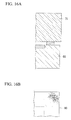
Fig. 14A is a plan view of a modified embodiment of the pressure sensor package. -
Fig. 14B is a plan view of another modified embodiment of the pressure sensor package. -
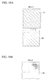
Fig. 15A is a plan view showing an exemplary arrangement of second bumps. -
Fig. 15B is a plan view showing another exemplary arrangement of the second bumps. -
Fig. 15C is a plan view showing a further exemplary arrangement of the second bumps. -
Fig. 15D is a plan view showing another exemplary arrangement of the second bumps. -
Fig. 16A is a side cross-sectional view of a main part of the pressure sensor package according to the invention mounted on an external substrate. -
Fig. 16B is a plan view showing a thermal stress distribution of the pressure sensor package ofFig. 16A . -
Fig. 17A is a side cross-sectional view of main part of a conventional pressure sensor package mounted on the external substrate. -
Fig. 17B is a plan view showing a thermal stress distribution of the pressure sensor package ofFig. 17A . -
Fig. 18A is a side cross-sectional view of a main part of a thick-section example of the pressure sensor package according to the invention mounted on the external substrate. -
Fig. 18B is a plan view showing a thermal stress distribution of the thick-section example of the pressure sensor package ofFig. 18A . -
Fig. 19A is a side cross-sectional view of a main part of a medium-section example of the pressure sensor package according to the invention mounted on the external substrate. -
Fig. 19B is plan view showing a thermal stress distribution of the medium-section example of the pressure sensor package ofFig. 19A . -
Fig. 20A is a side cross-sectional view of main part of a thin-section example of the pressure sensor package according to the invention mounted on the external substrate. -
Fig. 20B is a plan view showing a thermal stress distribution of the thin-section example of the pressure sensor package ofFig. 20A . -
Fig. 21 shows a relationship between the thickness (chip thickness) of the substrate and the maximum value of the thermal stress inside the substrate. -
- α, γ:
- central region
- β, δ:
- peripheral region
- 10, 20, 40:
- pressure sensor module
- 11, 21:
- pressure sensor
- 12, 22:
- semiconductor substrate
- 13,23:
- space,
- 14, 24:
- diaphragm section
- 15, 25:
- pressure sensitive element
- 16, 26:
- insulating section
- 17, 27:
- first conductive sections
- 18:
- first bump
- 28:
- first insulating section
- 29:
- second conductive sections
- 30:
- second bump
- 31:
- second insulating section
- 62:
- circuit
- 5:
- lamp
- Referring now to the drawings, the invention will be described in detail based on the embodiments thereof.
- The pressure sensor package of the invention includes two structures: a structure having a first bump on a first conductive section arranged at a peripheral region of a semiconductor substrate (a first pressure sensor package); and a structure including a second conductive section disposed on the first conductive section at the peripheral region of the semiconductor substrate, and having a second bump disposed on the second conductive section so as not to overlap with the first conductive section (second pressure sensor package). The embodiments described below are illustrative only, and the gauge arrangement, for example, is not limited thereto.
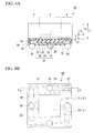
- Referring to
Figs. 1A, 1B and2 , a pressure sensor package (a first pressure sensor package) according to a first embodiment of the invention will be described.
Fig. 1A shows a cross section taken along line A-A of the pressure sensor package of the first embodiment shown inFig. 1B . - As shown in
Figs. 1A and 1B , apressure sensor 11 constituting the firstpressure sensor package 10 includes a plate-like semiconductor substrate 12 and a space (reference pressure room/cavity) 13 inside a plate-thickness direction central region α on a surface of thesemiconductor substrate 12. The space extends substantially parallel with the surface of thesemiconductor substrate 12. A thin-plate region above the space serves as adiaphragm section 14. Multiple pressure sensitive elements are arranged in thediaphragm section 14 so as to extend to the peripheral region. A firstconductive portion 17 is arranged on the peripheral region β excluding the diaphragm section on the surface and electrically connected to the pressuresensitive element 15. - As shown in the drawings, it is preferred that the peripheral region β excluding the first
conductive section 17 where thefirst bump 18 is provided is covered with a thin insulatingsection 16. The thin insulatingsection 16 may be a passivation film, such as a nitride film and an oxide film. In this structure, the pressuresensitive element 15 can be covered with the insulatingsection 16.
In thepressure sensor package 10 of the first embodiment, the entire peripheral region β is covered with the insulatingsection 16 excluding thefirst bump 18. Thus, when thefirst bump 18 is to be connected to an external substrate (not shown), the insulation property of the pressuresensitive element 15 with respect to the external substrate can be ensured.
The insulatingsection 16 blocks contact the pressuresensitive element 15 with the surrounding atmosphere, which improves corrosion resistance of the pressuresensitive element 15. The presence of the insulatingsection 16 significantly decreases external mechanical influence exerted directly on the pressuresensitive element 15 and not through thediaphragm section 14. - Each of the first
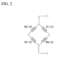
conductive sections 17 constituting thepressure sensor 11 includes thefirst bump 18 disposed thereon and electrically connected thereto. - Gauge resistance elements (R1 to R4) are provided on the surface of the
substrate 12. The gauge resistance elements function as pressuresensitive elements 15. The gauge resistance elements are electrically connected to one another via unillustrated lead wires to form a Wheatstone bridge (Fig. 2 ). The gauge resistance elements are preferably disposed at a peripheral portion of thediaphragm section 14. This is because both tensile stress and compression stress are often exerted on the pressuresensitive element 15, and thus a highly sensitive pressure sensor can be obtained. - As shown in
Fig. 1A , in thepressure sensor 11, the thickness D1 of the semiconductor substrate at the peripheral region, the thickness D2 of the diaphragm section, the height D3 of the space, and the remaining thickness D4 of the semiconductor substrate excluding D2 and D3 at the central region preferably satisfy the relationships: (D2+D3) << D4 and D 1 being nearly equal to D4.
In the first embodiment, D1 to D4 are selected so as to satisfy the above relationships. - If D1 to D4 satisfy the above relationships, the
pressure sensor 11 constituting the firstpressure sensor package 10 includes, in the central region α thereof, thediaphragm section 14 with a significantly smaller thickness D2 andspace 13 with a substantially smaller height D3 when seen from the surface of thesemiconductor substrate 12 from the thickness direction. The remaining section below (above, inFig. 1A ) thespace 13 has a thickness sufficiently larger than D1 to D3. A thickness D4 of thesemiconductor substrate 12 is designed to have a value substantially equal to the entire thickness D 1 of thesemiconductor substrate 12 in the peripheral region β. That is, the dimension (D2+D3), the sum of the thickness D2 of thediaphragm section 14 and the height D3 of thespace 13, is as small, for example, as 5 to 20 micrometers. The space height D3 is, for example, 1 to 3 micrometers.
Although the central region and the peripheral region are distinctively described, these regions are made from a single, integrated semiconductor substrate. - In a conventional sensor chip, a bonding wire is essentially required for packaging in order to prevent thermal influence such as a strain on the chip. As a result, the chip size cannot be made more compact. In the present embodiment (the invention), however, a bump is provided at the sensor chip to allow direct connection of the sensor chip to other elements via the bump.
A conventionally-required casing for containing the pressure sensor is not required in thepressure sensor package 10 of the first embodiment. Since the pressure sensor has thefirst bump 18 for connecting to an external substrate, the pressure sensor package can be made significantly compact. The components for the casing and the process for packaging the pressure sensor in the casing can be eliminated to significantly reduce manufacturing cost. Further, excellent connecting reliability can be obtained with the structure in which a connection is established only between thefirst bump 18 and the external substrate without using bonding wires or leads that may produce multiple electric connection sites. Note that the present embodiment is illustrative only, and may be subject to changes in the arrangement of the gauge resistance elements or lead resistance elements. - Next, with reference to
Figs. 3A and 3B , a second pressure sensor package according to a second embodiment of the invention will be described.
Fig. 3A shows a cross section taken along line B-B of the pressure sensor package of second embodiment shown inFig. 3B . - As shown in
Figs. 3A and 3B , apressure sensor 21 constituting the firstpressure sensor package 20 includes a plate-like semiconductor substrate 22 and a space (reference pressure cavity) 23 inside a plate-thickness direction central region α on a surface of thesemiconductor substrate 22. The space extends substantially parallel with the surface of thesemiconductor substrate 22. A thin-plate region above the space serves as adiaphragm section 24. Multiple pressure sensitive elements are arranged in thediaphragm section 24. A firstconductive portion 27 is arranged on the peripheral region δ excluding the diaphragm section on the surface and electrically connected to the pressuresensitive element 25. - As shown in the drawings, it is preferred that the peripheral region δ excluding the first
conductive section 27 where a secondconductive section 29 and thesecond bump 30 is provided is covered with a thin insulatingsection 26. The thin insulatingsection 26 may be a passivation film, such as s nitride film and an oxide film. In this structure, the pressuresensitive element 25 can be covered with the insulatingsection 26.
In thepressure sensor package 20 of the second embodiment, the entire peripheral region δ is covered with the insulatingsection 26 excluding the region where the firstconductive section 27 is to be provided. Thus, when thepressure sensor 21 is left or kept before the secondconductive section 29 and thesecond bump 30 is produced, the insulation property of the pressuresensitive element 25 with respect to the external substrate can be ensured.
The insulatingsection 26 blocks contact of the pressuresensitive element 25 with surrounding atmosphere, which improves corrosion resistance of the pressuresensitive element 25. The presence of the insulatingsection 26 significantly decreases external mechanical influence exerted directly from the outside on the pressuresensitive element 25 thereof, but not via thediaphragm section 24. - In the
pressure sensor package 20 according to the second embodiment, thepressure sensor 21 includes the first insulatingsection 28, the secondconductive section 29, and the second bump. The first insulatingsection 28 is disposed to cover the peripheral region δ. The secondconductive section 29 is disposed on the first insulatingsection 28, and is electrically connected to the firstconductive section 27. The second bump is electrically connected to the second conductive section at an area where the second conductive section does not overlap with the first conductive section. The first insulating section includes photosensitive resin, such as epoxy, as a stress buffer layer. - Gauge resistance elements (Rl to R4) are provided on the pressure
sensitive element 25 of the second embodiment in the same manner as that shown inFigs. 1A and 1B . Each of the gauge resistance elements is electrically connected to one another via unillustrated lead wires to form a Wheatstone bridge (Fig. 2 ). In this casing shown inFigs. 3A and 3B , the gauge resistance elements are preferably disposed at a peripheral portion of thediaphragm section 24 where both tensile stress and compression stress are often exerted. - As shown in
Fig. 3A , in thepressure sensor 21, the thickness T1 of the semiconductor substrate at the peripheral region, the thickness T2 of the diaphragm section, the height T3 of the space, and the remaining thickness T4 of the semiconductor substrate excluding T2 and T3 at the central region preferably satisfy the relationships: (T2+T3) << T4 and T1 being nearly equal to T4.
In the second embodiment, T1 to T4 are selected so as to satisfy the above relationships. - If T1 to T4 satisfy the above relationships, the
pressure sensor 21 constituting the secondpressure sensor package 20 includes, in the central region γ thereof, adiaphragm section 24 with a significantly small thickness T2 and aspace 23 with a substantially small height T3 when seen from the surface of thesemiconductor substrate 22 in the thickness direction. The remaining section below (above, inFig. 3A ) thespace 23 has a thickness sufficiently larger than T1 to T3. Thickness T4 of thesemiconductor substrate 22 is designed to have a value substantially equal to the entire thickness T1 of thesemiconductor substrate 22 in the peripheral region δ. That is, the dimension (T2+T3), the sum of the thickness T2 of thediaphragm section 24 and the height T3 of thespace 23, is, for example, as small as 5 to 20 micrometers. The space height T3 is, for example, 1 to 3 micrometers.
Although the central region and the peripheral region are distinctively described, these regions are made from a single, integrated semiconductor substrate. - In this structure, the second
conductive section 29 allows thesecond bump 30 to be disposed at any position on the peripheral region δ so as not to overlap with the firstconductive section 27. Thus, thesecond bump 30 may be provided at any connecting site according to the demand of the external substrate. As a result, thepressure sensor package 20 according to the second embodiment has a high degree of freedom on connecting sites with respect to the external substrate. - In a conventional sensor chip, a bonding wire is essentially required for packaging. As a result, the chip size cannot be made compact. In the present embodiment (the invention), however, the bump is provided at the sensor chip to allow direct connection of the sensor chip to other elements via the bump.
A conventionally-required casing for containing the pressure sensor is not required in thepressure sensor package 20 of the first embodiment. Since thesecond bump 30 for connecting to an external substrate is provided at the pressure sensor, the pressure sensor package can be made significantly compact. The components for the casing and the process for packaging the pressure sensor in the casing can be eliminated to significantly reduce manufacturing cost. Further, excellent connecting reliability can be obtained with a structure in which a connection is established only between thesecond bump 30 and the external substrate without using bonding wires or leads that may produce multiple electric connection sites. Note that the present embodiment is illustrative only, and may be subject to changes in the arrangement of the gauge resistance elements or lead resistance elements. - Next, with reference to
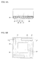
Figs. 4A and 4B , a pressure sensor package (based on the second pressure sensor package) according to a third embodiment of the invention will be described.Fig. 4A shows a cross section taken along line C-C of the pressure sensor package of the third embodiment shown inFig. 4B .
In thepressure sensor package 40 shown inFigs. 4A and 4B , a second insulatingsection 31 covers a peripheral region δ so that only thesecond bump 30 is exposed, based on the secondpressure sensor package 20 shown inFigs. 3A and 3B . The second insulating section is made of epoxy resin as in the first insulating section. - In the second
pressure sensor package 40 of the third embodiment, the entire peripheral region δ is covered with the second insulating section excluding thesecond bump 30. Thus, when thesecond bump 30 is to be connected to an external substrate (not shown), the insulation property of the secondconductive section 29 with respect to the external substrate can be ensured.
The second insulatingsection 31 blocks contact of the secondconductive section 29 with the surrounding atmosphere, which improves corrosion resistance of the secondconductive section 29. The presence of the second insulatingsection 31 significantly decreases external mechanical influence exerted on the secondconductive section 29. - A structure having various circuits provided inside the substrate that constitutes a main part of the sensor package will be described. Such a substrate is shown in
Figs. 5A and 5B. Fig. 5A shows a cross section taken along line D-D of the substrate shown inFig. 5B .
A pressure sensor package 60 which includes the substrate shown inFig. 5 is based on the firstpressure sensor package 10 and the secondpressure sensor package 20 shown inFigs. 1A to 4B . The pressure sensor package 60 has acircuit 62 provided at a peripheral region β (δ) of the semiconductor substrate 11 (21) where a first conductive section 17 (27) is not provided. Thecircuit 62 may be a signal amplification circuit or a compensation circuit. The first conductive section 17 (27) functions as an electrode pad.
Thecircuit 62 may be disposed at any position on the peripheral region β (δ) where they do not overlap with the diaphragm section 64, and is not limited to the described positions. To clearly show the physical relationship of the first conductive section 17 (27) and thecircuit 62 inFigs. 5A and 5B , illustration of other structures is omitted. - As in the first to third embodiments, since the pressure sensor package 60 includes the
circuit 62 inside of the substrate, conventionally-required external structures such as ASIC are no more required. The components for connection and the process for connecting can be eliminated to significantly reduce manufacturing cost. Thus, external physical or chemical influence on the substrate is eliminated to improve electric connecting performance. - Here, with reference to
Fig. 6 , an example in which a pressure sensor package according to the invention is mounted on an external substrate will be described.
It is shown inFig. 6 that apressure sensor package 72 is connected via its bump 73 to anexternal substrate 71 consisting of various kinds of printed circuit boards. That is, the pressure sensor package according to the invention may be mounted as a chip sized part.
To clearly show the mounting state inFig. 6 , illustration of other structures is omitted. Although the arrangement of the bump shown inFig. 6 is that of the pressure sensor package according to the second embodiment, the arrangement is not limited to the same. A chip-size packaging can also be applied to the pressure sensor package according to the first embodiment. - Referring now to
Figs. 7 to 10 , a manufacturing process of the second pressure sensor package according to the third embodiment shown inFigs. 4A and 4B will be described.
In the embodiments of the invention, processing for chip-size packaging is performed in a wafer level with respect to the pressure sensor. Such a pressure sensor having space (reference pressure room) 23 inside of the semiconductor substrate is produced in a method described in S. Armbruster et al., "A Novel Micromachining Process for the Fabrication of Monocrystalline SI-Membranes Using Porous Silicon", digest of technical papers transducers, March 2003, pp. 246. - First, as shown in
Figs. 7A and 7B , an insulatingresin layer 28 is formed in thepressure sensor 21 excluding the region where thediaphragm 24 is provided. In this method, photosensitive resin such as epoxy resin is applied to the entire surface of the wafer including the diaphragm. Then, the only resin on the diaphragm section is removed through exposure development and the remaining resin is formed as an insulating resin layer. In this process, the resin on the firstconductive section 27 functioning as an electrode pad is also removed to efficiently provide an opening for electric wiring. - Next, as shown in
Figs. 8A and 8B , the wiring layer/re-routing is formed as the secondconductive section 29 which electrically connects to the firstconductive section 27. Although the wiring layer is made of plated copper (Cu) in this method, the wiring layer may also be formed by other film deposition method including sputtering and CVD. In addition, other metallic materials including Au and Ni or the combination thereof may also be used. - Then, as shown in
Figs. 9A and 9B , the insulating resin layer is formed as the second insulatingsection 31 to include the secondconductive section 29 excluding the region where thediaphragm section 24 is provided. Then, photosensitive resin such as epoxy resin is applied to the entire surface of the wafer including the diaphragm. Then, the resin on the diaphragm section is removed through exposure development to efficiently provide an opening for bump formation. - Finally, as shown in
Figs. 10A and 10B , thebump 30 is formed so as to electrically connect to the wiring layer which constitutes the secondconductive section 29. Although the bump is formed by mounting a solder ball, the bump may also be formed in various methods including printing or plating. - The second pressure sensor package having the structure (the third embodiment) described in
Figs. 4A and 4B is manufactured in the process described above. The pressure sensor packages shown inFigs. 1A, 1B ,3A and 3B may also be manufactured in the similar method. - First, with reference to
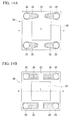
Figs. 13A and 13B , a pressure sensor package (a second pressure sensor package) according to a fourth embodiment of the invention will be described. InFigs. 13A and 13B , an insulating layer, such as passivation layer, is not shown.
Fig. 13A shows a cross section taken along line J-J of the pressure sensor package according to the fourth embodiment shown inFig. 13B . In thepressure sensor package 40 according to the third embodiment shown inFigs. 4A and 4B , the first insulating section is made in a continuous manner. In thepressure sensor package 50 according to the fourth embodiment shown inFigs. 13A and 13B , asecond bump 30 forms anisland structure 35.
In theisland structure 35, the first insulatingsection 28 and the second insulatingsection 31 near thesecond bump 30 are provided separately. - The
pressure sensor package 50 shown inFigs. 13A and 13B includes a secondconductive section 29 and a second insulatingsection 31 to cover the secondconductive section 29. The secondconductive section 29 is disposed on a first insulatingsection 28 and is electrically connected to a firstconductive section 27 that is partly exposed from the first insulatingsection 28. Thesecond bump 30 is disposed on the secondconductive section 29 at a position where the secondconductive section 29 is partly exposed through an opening formed in the second insulatingsection 31 so as not to overlap with the first conductive section.
With this structure, influence of the insulating section (insulating resin layer) exerted on the diaphragm section may be significantly reduced. As a result, the sensitivity of the diaphragm can be kept high to produce a highly accurate sensor. - As a secondary effect of forming the
island structure 35 corresponding to thesecond bump 30, a pressure passage S can be provided between theisland structures 35 for keeping the pressure of between thediaphragm section 24 and the pressure outside of thesemiconductor substrate 22 constant. - That is, the central region of the
semiconductor substrate 22 where thediaphragm section 24 is provided is not fully surrounded by the first insulatingsection 28 and the second insulatingsection 31. Thus, the passage S serves as a pressure inflow and outflow path of thesemiconductor substrate 22. - If such a
pressure sensor package 50 is disposed in a narrow conduit, for example, the external pressure is accurately transmitted to thediaphragm section 24 through the passage S between theisland structures 35. In this manner, when the pressure sensor packages 50 are closely disposed in a narrow environment, it is possible to measure the pressure accurately and stably. - Although the
island structure 35 is most preferably provided for eachsecond bump 30, several second bumps may also constitute theisland structure 35. - The arrangement of the
second bump 30 on thesemiconductor substrate 22 is not limited to that shown inFigs. 13A and 13B , in which thesecond bump 30 is disposed at a middle portion of each side of the peripheral region excluding thediaphragm section 24. Rather, as shown inFig. 14A , thesecond bump 30 may be disposed at a corner of the four sides of the peripheral region of thesemiconductor substrate 22 excluding the region where thediaphragm section 24 is provided. Theisland structure 35 surrounding thesecond bump 30 may be disposed so as to extend along with two sides in the four sides of the peripheral region. - With this structure, a wide opening may be provided along the longitudinal direction L of the
island structure 35 in which gas and fluid flow, so that the gas and fluid may flow smoothly. For example, if thepressure sensor package 50 is disposed in a long, narrow pressure passage such that the extending direction of the pressure passage coincides with the longitudinal direction L of theisland structure 35, the pressure variation in the pressure passage can be accurately detected. - In the structure of
Fig. 14A , although theisland structure 35 is formed in a teardrop shape when seen as a plan view, theisland structure 35 may also be formed in a rectangular shape as shown inFig. 14B . Further, theisland structure 35 may also be formed in various shapes including ellipse and infinite shape so long as a certain interval of theisland structures 35 is kept. - In order to verify the effect of the island structure, comparison was made on pressure sensing characteristics between the pressure sensor having the first and second insulating sections formed in island shapes and a conventional pressure sensor having a spreading insulating section. As a result, the former pressure sensor had greatly improved offset temperature characteristic that may change with external stress. Thus, the island structure in the present embodiment was verified to be effective in reduction of the influence of stress exerted on the diaphragm. Although the structure of the present embodiment has a second insulating resin layer, the same advantageous effect can be obtained in a structure with an island-shaped first insulating resin layer and no second insulating resin layer.
- Referring to
Figs. 15A to 15D , several patterns of forming second bumps of the pressure sensor package according to the invention will be described.
Fig. 15A shows an example in which thesecond bumps 30 are disposed at four corners of therectangular semiconductor substrate 22. The second bumps 30 are disposed symmetrically at equal intervals. In this manner, the stress is equally exerted on thesecond bumps 30 and thus variations in the detecting characteristics of apressure sensor package 90 can be suppressed.
Each of thesecond bumps 30 may also be disposed at a middle portion of each side of thesemiconductor substrate 22 in a symmetric manner at equal intervals as shown inFig. 15B . In this manner, the same advantageous effect as that of the structure shown inFig. 15A can obtained. - As shown in
Figs. 15C and 15D , thesecond bumps 30 disposed symmetrically at equal intervals are preferably formed at the same size. In this manner, the stress will be equally exerted on the second bumps 30. Thus, variations in the detecting characteristics of thepressure sensor package 90 can be prevented in the structure shown inFigs. 15A and 15B . Although an absolute pressure sensor has been described in the foregoing embodiments, a relative pressure sensor may also be employed. In the relative pressure sensor, a through hole is formed in the rest of the central section to extend to a space (formed inside the central region) so long as no stress is exerted on the diaphragm section. - Referring now to
Figs. 16A to 17B , operations and advantageous effects characteristic to the pressure sensor package according to the invention over a conventional structure will be described.
A simulation (experiment) was conducted to compare the package structure of the invention (Fig. 16A ) with a large substrate portion at an opposite side of the surface on which the diaphragm is provided to support the diaphragm and a conventional structure (Fig. 17A ) with no support (substrate portion).
Fig. 16A shows a typical example of apressure sensor package 80 according to the invention mounted on another substrate, namely, anexternal substrate 71.Fig. 16B shows the distribution of thermal stress around the bumps.
Fig. 17A shows a typical example of apressure sensor package 82 according to the invention mounted on another substrate, namely, anexternal substrate 71.Fig. 17B shows the distribution of thermal stress around the bumps.
As a result of the comparison with reference toFig. 16B andFig. 17B , the structure (typical example) of the invention was by far superior to the conventional structure in terms of thermal stress. That is, the structure of the invention generated by far smaller amounts of thermal stress. - Next, referring to
Figs. 18A to 20 , differences in operation and advantageous effects due to thickness (D 1 or T1) of the substrate in the pressure sensor package according to the invention will be described briefly.
The pressure sensor packages according to the invention having three different thicknesses were prepared and compared in a simulation (experiment). A thick-section (400 micrometers) example is shown inFig. 18A , a medium-section (200 micrometers) example is shown inFig. 19A , and a thin-section (100 micrometers) example is shown inFig. 20A .
Figs. 18B ,19B and20B each show the degree of distribution of thermal stress around the bumps of the mounted thick-section, medium-section, and thin-section examples, respectively.
As a result of a comparison, it was found that a satisfactory result could not be obtained with the thin-section example and that a certain thickness may be required to obtain satisfactory operation and advantageous effects.
Further experiment (heat reliability test) was conducted to find out the upper and lower limits of the optimum or practical substrate thickness. The condition was as follows. - -25 / 125 degree. C, 1000 cycles (the bumps were observed after 1000 cycles)
- sensor dimension: D2: 5 micrometers; D3: 2 micrometers; D1: 100, 150, 200, 300, 400 and 500 micrometers
- external substrate 71: a rigid substrate (FR4) having thickness of 1 mm
- The pressure sensor package according to the invention is used for measuring pressure, such as air pressure, water pressure and oil pressure. The pressure sensor package according to the invention is produced through wafer level chip-size packaging and thus requires no casing, and is suitable for various electronic parts to be made thin, compact and lightweight.
As a conclusion, the substrate thickness (D1 1 or T1) is preferably not less than 200 micrometers, and the practical upper limit (maximum thickness) is preferably about 500 micrometers in terms of mounting property.
Note that, in the simulations (experiments) described above, the drawings which show the thermal stress distribution are plan views of the portion where the semiconductor package and the bumps are connected. In
Claims (8)
- A pressure sensor package comprising:a pressure sensor including at least a first conductive portion having a space inside a central region on a surface of a semiconductor substrate, a thin-plate region above the space serving as a diaphragm section, and pressure sensitive elements arranged in the diaphragm section, the first conductive portion being arranged on a peripheral region excluding the diaphragm section on the surface and electrically connected to each of the pressure sensitive elements; anda first bump arranged on the first conductive portion and electrically connected to it,wherein the thickness D1 of the semiconductor substrate at the peripheral region, the thickness D2 of the diaphragm section, the height D3 of the space, and the remaining thickness D4 of the semiconductor substrate excluding D2 and D3 at the central region satisfy the relationships: (D2+D3) << D4, and D 1 being nearly equal to D4.
- A pressure sensor package comprising:a pressure sensor including at least a first conductive portion having a space inside a central region on a surface of a semiconductor substrate, a thin-plate region above the space serving as a diaphragm section, and pressure sensitive elements arranged in the diaphragm section, the first conductive portion being arranged on a peripheral region excluding the diaphragm section on the surface and electrically connected to each of the pressure sensitive elements;a first insulating section disposed so as to cover the peripheral region;a second insulating section disposed on the first insulating section and electrically connected to the first conductive section; anda second bump arranged on the second conductive portion and electrically connected to it at a position not overlapping with the first conductive section,wherein the thickness D1 of the semiconductor substrate at the peripheral region, the thickness D2 of the diaphragm section, the height D3 of the space, and the remaining thickness D4 of the semiconductor substrate excluding D2 and D3 at the central region satisfy the relationships: (D2+D3) << D4, and D1 being nearly equal to D4.
- The pressure sensor package according to claim 2, further comprising a second insulating section disposed so as to cover the peripheral region including the second conductive section with only the second bump exposed.
- The pressure sensor package according to claim 2, further comprising a second insulating section disposed to overlap with the first insulating section so as to cover the second conductive section with only the second bump exposed, wherein at least one of the first insulating section and the second insulating section is disposed in the vicinity of an island-shaped second bump.
- The pressure sensor package according to claim 2, wherein adjacent second bumps are symmetrically positioned.
- The pressure sensor package according to claim 1 or 2, further comprising an amplifier circuit and/or a compensating circuit inside the pressure sensor.
- The pressure sensor package according to claim 2, wherein the first insulating section is formed in an island shape.
- An electronic part including the pressure sensor package according to claim 1 or 2 mounted thereon.
Applications Claiming Priority (3)
| Application Number | Priority Date | Filing Date | Title |
|---|---|---|---|
| JP2006010961 | 2006-01-19 | ||
| JP2006256003 | 2006-09-21 | ||
| PCT/JP2007/050801 WO2007083748A1 (en) | 2006-01-19 | 2007-01-19 | Pressure sensor package and electronic part |
Publications (1)
| Publication Number | Publication Date |
|---|---|
| EP1975587A1 true EP1975587A1 (en) | 2008-10-01 |
Family
ID=38287698
Family Applications (1)
| Application Number | Title | Priority Date | Filing Date |
|---|---|---|---|
| EP07707089A Withdrawn EP1975587A1 (en) | 2006-01-19 | 2007-01-19 | Pressure sensor package and electronic part |
Country Status (5)
| Country | Link |
|---|---|
| US (1) | US7549344B2 (en) |
| EP (1) | EP1975587A1 (en) |
| JP (2) | JPWO2007083748A1 (en) |
| CN (1) | CN101375146B (en) |
| WO (1) | WO2007083748A1 (en) |
Families Citing this family (14)
| Publication number | Priority date | Publication date | Assignee | Title |
|---|---|---|---|---|
| EP2088411B1 (en) * | 2006-11-29 | 2015-05-06 | Fujikura Ltd. | Pressure sensor module |
| US8673769B2 (en) * | 2007-06-20 | 2014-03-18 | Lam Research Corporation | Methods and apparatuses for three dimensional integrated circuits |
| JP5331546B2 (en) * | 2008-04-24 | 2013-10-30 | 株式会社フジクラ | Pressure sensor module and electronic component |
| JP2010199148A (en) * | 2009-02-23 | 2010-09-09 | Fujikura Ltd | Semiconductor sensor device and method of manufacturing thereof, package and method of manufacturing thereof, module and method of manufacturing thereof, and electronic device |
| JP5216041B2 (en) * | 2010-04-07 | 2013-06-19 | ダイキン工業株式会社 | Transparent piezoelectric sheet with frame, each having transparent piezoelectric sheet, touch panel, and electronic device |
| US8378435B2 (en) | 2010-12-06 | 2013-02-19 | Wai Yew Lo | Pressure sensor and method of assembling same |
| CN102589753B (en) | 2011-01-05 | 2016-05-04 | 飞思卡尔半导体公司 | Pressure sensor and method for packing thereof |
| US8511171B2 (en) * | 2011-05-23 | 2013-08-20 | General Electric Company | Device for measuring environmental forces and method of fabricating the same |
| US9029999B2 (en) | 2011-11-23 | 2015-05-12 | Freescale Semiconductor, Inc. | Semiconductor sensor device with footed lid |
| JP5935352B2 (en) * | 2012-01-27 | 2016-06-15 | 富士電機株式会社 | Manufacturing method of physical quantity sensor having SON structure. |
| US9297713B2 (en) | 2014-03-19 | 2016-03-29 | Freescale Semiconductor,Inc. | Pressure sensor device with through silicon via |
| US9362479B2 (en) | 2014-07-22 | 2016-06-07 | Freescale Semiconductor, Inc. | Package-in-package semiconductor sensor device |
| CN107527874B (en) | 2016-06-20 | 2023-08-01 | 恩智浦美国有限公司 | Cavity type pressure sensor device |
| CN107941407B (en) * | 2017-11-19 | 2019-05-21 | 东北大学 | A kind of micro-voltage high-overload sensor chip |
Family Cites Families (16)
| Publication number | Priority date | Publication date | Assignee | Title |
|---|---|---|---|---|
| JPH0495740A (en) * | 1990-08-06 | 1992-03-27 | Toyota Autom Loom Works Ltd | Semiconductor device |
| JPH08210935A (en) * | 1995-02-07 | 1996-08-20 | Tokai Rika Co Ltd | Pressure sensor |
| US6809421B1 (en) * | 1996-12-02 | 2004-10-26 | Kabushiki Kaisha Toshiba | Multichip semiconductor device, chip therefor and method of formation thereof |
| JP4074051B2 (en) | 1999-08-31 | 2008-04-09 | 株式会社東芝 | Semiconductor substrate and manufacturing method thereof |
| JP2002082009A (en) * | 2000-06-30 | 2002-03-22 | Denso Corp | Pressure sensor |
| JP4250868B2 (en) | 2000-09-05 | 2009-04-08 | 株式会社デンソー | Manufacturing method of semiconductor pressure sensor |
| JP2002340714A (en) | 2001-05-15 | 2002-11-27 | Matsushita Electric Works Ltd | Semiconductor pressure sensor and its manufacturing method |
| JP2004170148A (en) * | 2002-11-18 | 2004-06-17 | Fujikura Ltd | Absolute pressure type pressure sensor module |
| JP4322508B2 (en) * | 2003-01-15 | 2009-09-02 | 新光電気工業株式会社 | Manufacturing method of semiconductor device |
| CN1739014B (en) | 2003-01-30 | 2010-05-05 | 株式会社藤仓 | Semiconductor pressure sensor and process for fabricating the same |
| JP2006010961A (en) | 2004-06-24 | 2006-01-12 | Mitsubishi Cable Ind Ltd | Photonic crystal fiber and laser processing machine |
| JP2006105624A (en) * | 2004-09-30 | 2006-04-20 | Sumitomo Osaka Cement Co Ltd | Diaphragm chip, pressure sensor using it, and method for manufacturing diaphragm chip |
| JP2006256003A (en) | 2005-03-16 | 2006-09-28 | Honda Motor Co Ltd | Structure panel |
| JP2006324320A (en) * | 2005-05-17 | 2006-11-30 | Renesas Technology Corp | Semiconductor device |
| JP2007234881A (en) * | 2006-03-01 | 2007-09-13 | Oki Electric Ind Co Ltd | Semiconductor device laminating semiconductor chips, and its manufacturing method |
| JP4955349B2 (en) * | 2006-09-07 | 2012-06-20 | 新光電気工業株式会社 | Semiconductor device |
-
2007
- 2007-01-19 CN CN2007800031760A patent/CN101375146B/en not_active Expired - Fee Related
- 2007-01-19 EP EP07707089A patent/EP1975587A1/en not_active Withdrawn
- 2007-01-19 JP JP2007533809A patent/JPWO2007083748A1/en active Pending
- 2007-01-19 WO PCT/JP2007/050801 patent/WO2007083748A1/en active Application Filing
-
2008
- 2008-07-17 US US12/175,245 patent/US7549344B2/en not_active Expired - Fee Related
-
2009
- 2009-05-18 JP JP2009120413A patent/JP4991788B2/en not_active Expired - Fee Related
Non-Patent Citations (1)
| Title |
|---|
| See references of WO2007083748A1 * |
Also Published As
| Publication number | Publication date |
|---|---|
| WO2007083748A1 (en) | 2007-07-26 |
| CN101375146B (en) | 2010-08-11 |
| JPWO2007083748A1 (en) | 2009-06-11 |
| CN101375146A (en) | 2009-02-25 |
| JP2009180746A (en) | 2009-08-13 |
| US7549344B2 (en) | 2009-06-23 |
| US20080276713A1 (en) | 2008-11-13 |
| JP4991788B2 (en) | 2012-08-01 |
Similar Documents
| Publication | Publication Date | Title |
|---|---|---|
| US7549344B2 (en) | Pressure sensor package and electronic part | |
| JP4617943B2 (en) | Mechanical quantity measuring device | |
| US7530276B2 (en) | Semiconductor pressure sensor and manufacturing method thereof | |
| CN101389940B (en) | Pressure sensor with silicon frit bonded cap | |
| EP1947439B1 (en) | Semiconductor pressure sensor | |
| US7051595B2 (en) | Monolithic multi-functional integrated sensor and method for fabricating the same | |
| US7849749B2 (en) | Pressure sensor module | |
| EP2388816A1 (en) | Semiconductor sensor device, method of manufacturing semiconductor sensor device, package, method of manufacturing package, module, method of manufacturing module, and electronic device | |
| EP1008837A1 (en) | Rugged fluid flow and property microsensor | |
| US8127617B2 (en) | Pressure sensor, manufacturing method thereof, and electronic component provided therewith | |
| JP2006329929A (en) | Semiconductor pressure sensor | |
| JP2008039760A (en) | Pressure sensor | |
| KR20170101794A (en) | Semiconductor pressure sensor for harsh media application | |
| JP2014048072A (en) | Pressure sensor module | |
| JP5331546B2 (en) | Pressure sensor module and electronic component | |
| JP5057606B2 (en) | Electronic component and manufacturing method | |
| US7109842B1 (en) | Robust fluid flow and property microsensor made of optimal material | |
| JP3908266B2 (en) | Semiconductor pressure sensor and manufacturing method thereof | |
| JP6714439B2 (en) | Strain detector and manufacturing method thereof | |
| JP2006250550A (en) | Sensor | |
| JP4207846B2 (en) | Pressure sensor | |
| JP7370819B2 (en) | sensor chip | |
| JP5779487B2 (en) | Pressure sensor module | |
| JP2010071817A (en) | Semiconductor sensor built-in package | |
| US20080041157A1 (en) | Acceleration sensor and method of manufacturing the same |
Legal Events
| Date | Code | Title | Description |
|---|---|---|---|
| PUAI | Public reference made under article 153(3) epc to a published international application that has entered the european phase |
Free format text: ORIGINAL CODE: 0009012 |
|
| 17P | Request for examination filed |
Effective date: 20080724 |
|
| AK | Designated contracting states |
Kind code of ref document: A1 Designated state(s): DE IT |
|
| DAX | Request for extension of the european patent (deleted) | ||
| RBV | Designated contracting states (corrected) |
Designated state(s): DE IT |
|
| STAA | Information on the status of an ep patent application or granted ep patent |
Free format text: STATUS: THE APPLICATION HAS BEEN WITHDRAWN |
|
| 18W | Application withdrawn |
Effective date: 20131018 |