EP1987346B1 - Dome gas sensor - Google Patents
Dome gas sensor Download PDFInfo
- Publication number
- EP1987346B1 EP1987346B1 EP07705132A EP07705132A EP1987346B1 EP 1987346 B1 EP1987346 B1 EP 1987346B1 EP 07705132 A EP07705132 A EP 07705132A EP 07705132 A EP07705132 A EP 07705132A EP 1987346 B1 EP1987346 B1 EP 1987346B1
- Authority
- EP
- European Patent Office
- Prior art keywords
- radiation
- gas sensor
- detector
- radiation source
- radiation detector
- Prior art date
- Legal status (The legal status is an assumption and is not a legal conclusion. Google has not performed a legal analysis and makes no representation as to the accuracy of the status listed.)
- Not-in-force
Links
- 230000005855 radiation Effects 0.000 claims abstract description 129
- 230000003287 optical effect Effects 0.000 claims description 30
- 239000000758 substrate Substances 0.000 claims description 22
- 238000005476 soldering Methods 0.000 claims description 6
- 238000004026 adhesive bonding Methods 0.000 claims description 3
- 239000012141 concentrate Substances 0.000 claims description 2
- 239000007789 gas Substances 0.000 description 58
- 229910002092 carbon dioxide Inorganic materials 0.000 description 9
- 230000008901 benefit Effects 0.000 description 7
- 239000011248 coating agent Substances 0.000 description 5
- 238000000576 coating method Methods 0.000 description 5
- 238000012545 processing Methods 0.000 description 5
- 238000010521 absorption reaction Methods 0.000 description 4
- 238000001514 detection method Methods 0.000 description 4
- 230000000694 effects Effects 0.000 description 4
- 230000004044 response Effects 0.000 description 4
- XVIZMMSINIOIQP-UHFFFAOYSA-N 1,2-dichloro-3-(2-chlorophenyl)benzene Chemical compound ClC1=CC=CC(C=2C(=CC=CC=2)Cl)=C1Cl XVIZMMSINIOIQP-UHFFFAOYSA-N 0.000 description 3
- CURLTUGMZLYLDI-UHFFFAOYSA-N Carbon dioxide Chemical compound O=C=O CURLTUGMZLYLDI-UHFFFAOYSA-N 0.000 description 3
- 238000004378 air conditioning Methods 0.000 description 3
- 238000013459 approach Methods 0.000 description 3
- 238000010438 heat treatment Methods 0.000 description 3
- 238000003384 imaging method Methods 0.000 description 3
- 239000003507 refrigerant Substances 0.000 description 3
- JAYCNKDKIKZTAF-UHFFFAOYSA-N 1-chloro-2-(2-chlorophenyl)benzene Chemical compound ClC1=CC=CC=C1C1=CC=CC=C1Cl JAYCNKDKIKZTAF-UHFFFAOYSA-N 0.000 description 2
- 101100084627 Neurospora crassa (strain ATCC 24698 / 74-OR23-1A / CBS 708.71 / DSM 1257 / FGSC 987) pcb-4 gene Proteins 0.000 description 2
- 238000004891 communication Methods 0.000 description 2
- 230000003993 interaction Effects 0.000 description 2
- 238000004519 manufacturing process Methods 0.000 description 2
- 239000000463 material Substances 0.000 description 2
- 238000000034 method Methods 0.000 description 2
- 239000004033 plastic Substances 0.000 description 2
- 230000008569 process Effects 0.000 description 2
- 239000002904 solvent Substances 0.000 description 2
- JBRZTFJDHDCESZ-UHFFFAOYSA-N AsGa Chemical compound [As]#[Ga] JBRZTFJDHDCESZ-UHFFFAOYSA-N 0.000 description 1
- 230000005457 Black-body radiation Effects 0.000 description 1
- UGFAIRIUMAVXCW-UHFFFAOYSA-N Carbon monoxide Chemical compound [O+]#[C-] UGFAIRIUMAVXCW-UHFFFAOYSA-N 0.000 description 1
- 208000001408 Carbon monoxide poisoning Diseases 0.000 description 1
- 208000005374 Poisoning Diseases 0.000 description 1
- BQCADISMDOOEFD-UHFFFAOYSA-N Silver Chemical compound [Ag] BQCADISMDOOEFD-UHFFFAOYSA-N 0.000 description 1
- LVQULNGDVIKLPK-UHFFFAOYSA-N aluminium antimonide Chemical compound [Sb]#[Al] LVQULNGDVIKLPK-UHFFFAOYSA-N 0.000 description 1
- 230000003321 amplification Effects 0.000 description 1
- MCMSPRNYOJJPIZ-UHFFFAOYSA-N cadmium;mercury;tellurium Chemical class [Cd]=[Te]=[Hg] MCMSPRNYOJJPIZ-UHFFFAOYSA-N 0.000 description 1
- 239000001569 carbon dioxide Substances 0.000 description 1
- 229910002091 carbon monoxide Inorganic materials 0.000 description 1
- 239000000567 combustion gas Substances 0.000 description 1
- 238000002485 combustion reaction Methods 0.000 description 1
- 238000009833 condensation Methods 0.000 description 1
- 230000005494 condensation Effects 0.000 description 1
- 238000010276 construction Methods 0.000 description 1
- 230000001419 dependent effect Effects 0.000 description 1
- 238000013461 design Methods 0.000 description 1
- 238000005516 engineering process Methods 0.000 description 1
- 230000007613 environmental effect Effects 0.000 description 1
- 238000004880 explosion Methods 0.000 description 1
- NBVXSUQYWXRMNV-UHFFFAOYSA-N fluoromethane Chemical compound FC NBVXSUQYWXRMNV-UHFFFAOYSA-N 0.000 description 1
- 238000010348 incorporation Methods 0.000 description 1
- 229910052738 indium Inorganic materials 0.000 description 1
- APFVFJFRJDLVQX-UHFFFAOYSA-N indium atom Chemical compound [In] APFVFJFRJDLVQX-UHFFFAOYSA-N 0.000 description 1
- 238000002347 injection Methods 0.000 description 1
- 239000007924 injection Substances 0.000 description 1
- 238000002955 isolation Methods 0.000 description 1
- 238000005259 measurement Methods 0.000 description 1
- 239000000203 mixture Substances 0.000 description 1
- 238000012986 modification Methods 0.000 description 1
- 230000004048 modification Effects 0.000 description 1
- 239000002991 molded plastic Substances 0.000 description 1
- 238000003199 nucleic acid amplification method Methods 0.000 description 1
- 238000001579 optical reflectometry Methods 0.000 description 1
- 231100000572 poisoning Toxicity 0.000 description 1
- 230000000607 poisoning effect Effects 0.000 description 1
- 238000004064 recycling Methods 0.000 description 1
- 239000004065 semiconductor Substances 0.000 description 1
- 230000035945 sensitivity Effects 0.000 description 1
- 229910052709 silver Inorganic materials 0.000 description 1
- 239000004332 silver Substances 0.000 description 1
- 239000007787 solid Substances 0.000 description 1
- 238000012546 transfer Methods 0.000 description 1
- 238000009966 trimming Methods 0.000 description 1
- 238000009423 ventilation Methods 0.000 description 1
- 238000003466 welding Methods 0.000 description 1
Images


Classifications
-
- G—PHYSICS
- G01—MEASURING; TESTING
- G01N—INVESTIGATING OR ANALYSING MATERIALS BY DETERMINING THEIR CHEMICAL OR PHYSICAL PROPERTIES
- G01N21/00—Investigating or analysing materials by the use of optical means, i.e. using sub-millimetre waves, infrared, visible or ultraviolet light
- G01N21/01—Arrangements or apparatus for facilitating the optical investigation
- G01N21/03—Cuvette constructions
-
- G—PHYSICS
- G01—MEASURING; TESTING
- G01J—MEASUREMENT OF INTENSITY, VELOCITY, SPECTRAL CONTENT, POLARISATION, PHASE OR PULSE CHARACTERISTICS OF INFRARED, VISIBLE OR ULTRAVIOLET LIGHT; COLORIMETRY; RADIATION PYROMETRY
- G01J3/00—Spectrometry; Spectrophotometry; Monochromators; Measuring colours
- G01J3/02—Details
- G01J3/0205—Optical elements not provided otherwise, e.g. optical manifolds, diffusers, windows
- G01J3/0216—Optical elements not provided otherwise, e.g. optical manifolds, diffusers, windows using light concentrators or collectors or condensers
-
- G—PHYSICS
- G01—MEASURING; TESTING
- G01J—MEASUREMENT OF INTENSITY, VELOCITY, SPECTRAL CONTENT, POLARISATION, PHASE OR PULSE CHARACTERISTICS OF INFRARED, VISIBLE OR ULTRAVIOLET LIGHT; COLORIMETRY; RADIATION PYROMETRY
- G01J3/00—Spectrometry; Spectrophotometry; Monochromators; Measuring colours
- G01J3/28—Investigating the spectrum
- G01J3/42—Absorption spectrometry; Double beam spectrometry; Flicker spectrometry; Reflection spectrometry
-
- G—PHYSICS
- G01—MEASURING; TESTING
- G01N—INVESTIGATING OR ANALYSING MATERIALS BY DETERMINING THEIR CHEMICAL OR PHYSICAL PROPERTIES
- G01N21/00—Investigating or analysing materials by the use of optical means, i.e. using sub-millimetre waves, infrared, visible or ultraviolet light
- G01N21/01—Arrangements or apparatus for facilitating the optical investigation
- G01N21/03—Cuvette constructions
- G01N21/031—Multipass arrangements
-
- G—PHYSICS
- G01—MEASURING; TESTING
- G01N—INVESTIGATING OR ANALYSING MATERIALS BY DETERMINING THEIR CHEMICAL OR PHYSICAL PROPERTIES
- G01N21/00—Investigating or analysing materials by the use of optical means, i.e. using sub-millimetre waves, infrared, visible or ultraviolet light
- G01N21/17—Systems in which incident light is modified in accordance with the properties of the material investigated
- G01N21/25—Colour; Spectral properties, i.e. comparison of effect of material on the light at two or more different wavelengths or wavelength bands
- G01N21/31—Investigating relative effect of material at wavelengths characteristic of specific elements or molecules, e.g. atomic absorption spectrometry
- G01N21/35—Investigating relative effect of material at wavelengths characteristic of specific elements or molecules, e.g. atomic absorption spectrometry using infrared light
- G01N21/3504—Investigating relative effect of material at wavelengths characteristic of specific elements or molecules, e.g. atomic absorption spectrometry using infrared light for analysing gases, e.g. multi-gas analysis
-
- G—PHYSICS
- G01—MEASURING; TESTING
- G01N—INVESTIGATING OR ANALYSING MATERIALS BY DETERMINING THEIR CHEMICAL OR PHYSICAL PROPERTIES
- G01N33/00—Investigating or analysing materials by specific methods not covered by groups G01N1/00 - G01N31/00
-
- G—PHYSICS
- G01—MEASURING; TESTING
- G01N—INVESTIGATING OR ANALYSING MATERIALS BY DETERMINING THEIR CHEMICAL OR PHYSICAL PROPERTIES
- G01N33/00—Investigating or analysing materials by specific methods not covered by groups G01N1/00 - G01N31/00
- G01N33/0004—Gaseous mixtures, e.g. polluted air
- G01N33/0009—General constructional details of gas analysers, e.g. portable test equipment
-
- G—PHYSICS
- G01—MEASURING; TESTING
- G01N—INVESTIGATING OR ANALYSING MATERIALS BY DETERMINING THEIR CHEMICAL OR PHYSICAL PROPERTIES
- G01N2201/00—Features of devices classified in G01N21/00
- G01N2201/06—Illumination; Optics
- G01N2201/062—LED's
-
- G—PHYSICS
- G01—MEASURING; TESTING
- G01N—INVESTIGATING OR ANALYSING MATERIALS BY DETERMINING THEIR CHEMICAL OR PHYSICAL PROPERTIES
- G01N2201/00—Features of devices classified in G01N21/00
- G01N2201/06—Illumination; Optics
- G01N2201/063—Illuminating optical parts
- G01N2201/0636—Reflectors
-
- G—PHYSICS
- G01—MEASURING; TESTING
- G01N—INVESTIGATING OR ANALYSING MATERIALS BY DETERMINING THEIR CHEMICAL OR PHYSICAL PROPERTIES
- G01N33/00—Investigating or analysing materials by specific methods not covered by groups G01N1/00 - G01N31/00
- G01N33/0004—Gaseous mixtures, e.g. polluted air
- G01N33/0009—General constructional details of gas analysers, e.g. portable test equipment
- G01N33/0027—General constructional details of gas analysers, e.g. portable test equipment concerning the detector
- G01N33/0036—Specially adapted to detect a particular component
- G01N33/004—Specially adapted to detect a particular component for CO, CO2
Definitions
- HVAC heating, ventilation and air conditioning
- gas sensors are used to provide safety from carbon monoxide poisoning. Furthermore, combustion gas sensing provides safety from an explosion risk.
- WO0007411 A1 discloses a blackbody radiation device that includes a planar filament emission element and a planar detector for respectively producing and detecting radiation; a reflector; a window; an electrical control; and a data output element.
- the arc length tends to zero.
- the surface is configured to reflect radiation from the radiation source to a corresponding location on the radiation detector, irrespective of the radiation exit angle from the radiation source.
- the surface is configured to reflect radiation leaving the centre of the radiation source to the centre of the radiation detector, radiation leaving the outer side of the radiation source to the outer side of the radiation detector, and radiation leaving the inner side of the radiation source to the inner side of the radiation detector.
- the reflecting means comprises a reflective surface of a housing.
- the radiation source and radiation detector are mounted on a common substrate configured to locate the radiation source and radiation detector in relation to the housing.
- the elongate member is adjustable by sliding of pins.
- the adjustable elongate member is lockable with respect to the reflecting means.
- the adjustable elongate member is lockable by soldering the pins.
- the reflecting means is arranged such that the optical path is defined at least in part by a cavity extending around the radiation source and radiation detector.
- the cavity is bounded by a plane parallel to surfaces of the radiation source and the radiation detector.
- the surface is configured such that radiation originating from a point on the radiation source is unfocussed as it converges on the radiation detector.
- FIG 1 a partial cross section of a gas sensor in accordance with a first embodiment of the present invention is shown.
- the gas sensor has a screen 1 in between a LED radiation source 2 and a photodiode radiation detector 3 on a substrate 4 mounted within the gas sensor.
- the LED and photodiode are thereofore side-by-side, with the screen in line and in between them.
- Only half of a housing 5 and the radiation path is shown in figure 1 .
- the housing has radial symmetry centred on the LED/screen/photodiode assembly.
- the inner surface 6 of the housing is reflective. This may be achieved by applying a reflective coating to a moulded plastic housing. Light rays 8 that diverge from the LED are reflected from the inner surface of the housing.
- the housing is shaped such that the light emitted by the LED is reflected through the cavity extending around the LED and photodiode and the reflected light rays 9 are concentrated onto the photodiode.
- the cavity is bounded by the plane parallel to the main emitting and absorbing surfaces of the LED and photodiode respectively.
- the rays reflected from surface 6 may or may not be focused.
- the curved shape of the housing is arranged to provide an even, broad spread of the light throughout the cavity.
- the surface may be hemispherical or semi-ellipsoidal.
- the even spread of light through the cavity is generally characterised by avoidance of focus where light rays originating from a point on the source do not converge on a particular focal point, but none the less converge on the photodiode.
- the side-by-side geometry has the advantage of allowing a small housing with a maximum spread of the interacting light path throughout the available volume of the housing. This provides good optical absorption efficiency and minimises the risk of saturation of the gas's interaction with the light, all in a compact housing.
- the compact optical design enables the gas sensor to fit within a 20mm diameter and 17mm long form factor. These features improve the gas sensor's sensitivity for gas sensing and response and the compact size makes it suitable for use in a wide range of space sensitive applications, where large housings are not acceptable.
- the LED has a narrow emission bandwidth, therefore using a LED and photodiode the narrow optical bandwidth required for gas sensing may be achieved without optical filters as are required for incandescent and other sources.
- the radiation source may be a LED that uses an optical bandpass filter to trim the optical emission profile but remove all other light frequencies that may cause error in the gas sensing process.
- Such an optical bandpass filter may remove no more than 25% of the emitted light form the LED, whereas in the prior art case of an incandescent source the vast majority of radiated light would be removed by the filter. Therefore, the LED radiates a precise and narrow bandwidth which is not post or pre optically filtered other than by simple bandwidth trimming.
- Figure 2 shows a cross section of the radiation source, screen and radiation detector is shown.
- the LED radiation source 2 and the photodiode radiation detector 3 are side-by-side mounted on an interconnecting substrate 4, with the screen 1 in between.
- the screen may be formed as part of the substrate and the LED and/or photodiode may abut the screen.
- the screen may be reflecting.
- the surfaces of the LED and/or photodiode facing the screen may be reflecting.
- the screen may be a reflective coating on one or more of the surfaces of the LED or photodiode facing each other.
- Both the radiation source and detector in this embodiment are based on the narrow band gap III-V material indium aluminium antimonide (In (1-x) Al x Sb), grown on a gallium arsenide (GaAs) substrate, the band gap of which can be tuned to a very narrow width to provide light emission and detection that is specific to carbon dioxide (C0 2 ) and carbon monoxide (CO gases) or other selected gases without the use of expensive optical filters and complicated differentiating circuitry.
- the LED and photodiode may be fabricated from the same semiconducting substrate.
- the invention is not limited to this type of radiation source and radiation detector.
- cadmium mercury telluride compounds are useful with ultraviolet frequencies.
- solid state radiation sources and detectors are convenient for miniaturised application, the present invention may also be implemented using incandescent sources and pyro-electric or thermopile detectors.
- the interconnecting substrate 4 and/or screen is thermally conductive and provides thermal communication between the LED and the photodiode.
- the thermal communication allows the transfer of heat from the LED to the photodiode. This provides the advantage of reducing the temperature difference between the LED and photodiode, thereby simplifying the compensation of any temperature dependent effects on the operation of the LED and/or photodiode. This approach is in contrast to most common electrical applications of conductive layers where the heat is transferred away from the semiconductors.
- the heating effect may be used to keep the photodiode at an elevated temperature when compared to its surroundings, thus keeping it on the positive side of the dew point of the ambient gas, therefore reducing the risk of condensation forming on the photodiode.
- the substrate may have integrated in it or mounted on it a temperature control means 12 such as a heater or cooler (Peltier device or similar) that can be controlled and powered to affect the temperature of the LED and photodiode simultaneously.
- a temperature control means 12 such as a heater or cooler (Peltier device or similar) that can be controlled and powered to affect the temperature of the LED and photodiode simultaneously.
- Temperature detection maybe achieved by use of an additional device (not shown), which may be in or on the substrate, such as a thermistor, or may be detected by measuring the characteristics of either the emitter or detector. For example the forward voltage of the LED will vary with temperature.
- the substrate provides a structural mounting for the LED and photodiode within the gas sensor.
- the substrate may be shaped to aid in locating the radiation source or detector for mounting on the substrate.
- the substrate may also provide mechanical features that serve to precisely locate the optical pair within the optical housing avoiding the need for adjustment or setting during the assembly process.
- the LED and photodiode are each provided with optically reflective layers 10, 11 on their surfaces. These reflective layers may be included on one or other of the LED and photodiode, or not at all.
- the reflective layers may be part of the substrate or applied as a coating to the back and/or sides of the LED and/or photodiode.
- the optical reflection improves the efficiency of both the LED and the photodiode. A proportion of the light generated or detected can pass straight through either device without being absorbed, however the incorporation of the reflective layers functions to return the light back through the LED improving emission efficiency, or similarly in the case of the photodiode, it can significantly increase the absorption by reducing loss of light out of the back or sides of the photodiode.
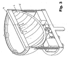
- FIG 3 a cross section of a second embodiment of a gas sensor is shown.
- the elements are numbered as in figure 1 .
- the domed reflector has been inverted.
- the substrate is an elongate printed circuit board extending along a diameter of the domed reflecting housing, which has radial symmetry.
- This substrate allows the mounting of further components (not shown).
- These components can include a temperature sensor (12 in figure 2 ) that because of the side-by-side mounting of the LED and photodiode allows the measurement simultaneously by one sensor of the temperature of both the LED and the photodiode. This has the advantage of reducing the component count.
- a preamplifier may be mounted on the substrate next to the LED/photodiode pair with the remaining electronics and processing components being located at the next available position on the substrate away from the LED/photodiode pair.
- the preamplifier and processor are located adjacent to both the LED and the photodiode. Any electrical modulation signals can be transmitted to the LED with minimised noise pickup.
- the same components can detect the signal from the photodiode, which may be in the nA range.
- FIG. 4 a perspective view of the second embodiment of a gas sensor is shown.
- Two gas filters 13, 14 are shown with the very narrow printed circuit board (PCB) 4 being located in the middle of them.
- PCB printed circuit board
- the signal processing and temperature control components 15 are located on the emitter/collector PCB as discussed above, they are placed on a second PCB 16.
- Having the preamplifier thus separated from the LED/photodiode pair has been enabled by the use of a centre tap connection in the centre of an array of discrete photodiode elements that make up the radiation detector connected along with the other two LED terminations by pins 17 to either:
- a tubular external housing (not shown) may be placed around the assembly, which forms a Faraday cage between the metalised reflector, the external tube and a shielding layer built into the second PCB, so improving the electrical isolation of the components, as well as being a structural support.
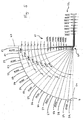
- Figure 5 shows a cross section of half of the internal surface 6 of the dome in another embodiment of the present invention.
- the dome has an internal surface comprising a plurality of sub surfaces 51 to 59, shown in section as arcs, each defined by a radius R9.3711 to R9.0104 respectively and a centre point 60, each sub surface being tangent to an adjacent sub surface and having a different radius and different centre location from the adjacent subsurface.
- the offsets of the centre points 61, 62 from the perpendicular datum lines 63 and 64 respectively are also shown.
- the emitter and detector lie on the datum line 64.
- the surface is defined by the arcs labelled 51 to 59 (and their reflection about datum line 63) being swept out by rotation by 180 degrees around datum line 64.
- Another embodiment may have the arc length tending to zero, thus giving a continuously varying curve from datum line 63 to datum line 64.
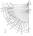
- the dome functions to reflect, as near as possible, the radiation from the emitter 2 through a single reflection to the identical mirrored location on the detector 3, irrespective of the radiation exit angle from the emitter. This is illustrated by Figures 6 and 7 .
- light rays 65, 66 leaving the centre 67 of the emitter 2 are reflected by the inner surface 6 as rays 68, 69 to the centre of the detector 70.
- Light rays 71, 72 leaving the outer side 73 of the emitter 2 are reflected as rays 74, 75 to the outer side of the detector 76.
- the emitter and detector are positioned on a common mounting a small distance apart, typically 3mm centre to centre.
- the mutually tangent radii forming the swept profile of the toroid are constructed such that the path length from emitter and detector is on average equal.
- the number of tangent radii used to construct the swept profile of the toroid determines the variation in path length for each ray angle between emitter and detector, therefore the statement that the path length for each specific radii is on average equal refers to the average path length of each radius, which generally occurs at the radius mid point.. Therefore, apart from one specific point in each radius, the path length varies continuously across the face of each radius and therefore the face of the toroidal swept curve, within the limits imposed by the number of radii selected in the construction of the swept curve.
- This dome has the effect of transferring the image of the emitter to the detector, without a focus.
- the image may be concentrated towards the centre of the detector when the components become out of alignment. This increases the manufacturing tolerance of the assembly.
- the surface is formed by silver coating an injection moulded feature that forms part of the sensor housing and does not provide a mounting for the emitter and detector.
- the emitter 2 and detector 3 are bonded to a bridge PCB (printed circuit board) 4 that serves to provide electrical connectivity, thermal path, and a mounting means that is adjustable on assembly to optimise the location of the reflected radiation pool on the detector.
- a bridge PCB printed circuit board
- Other components are labelled as in previous figures.
- a typical surface emitting LED may have an emission surface that is 1 mm 2 in area, and the location of the bridge mounting the emitter and detector is adjusted to provide as near as possible a pool of radiation (nearly identical to that radiated) striking the detector photodiode (as the non-focussed lighting provides greater efficiency) that is the same size. If the bridge PCB is wrongly adjusted in either direction, at no time will the total emitted radiation focus to a single point.
- the adjustment is performed when the bridge PCB is raised or lowered in the direction shown 83 in response to feedback, such as the detector received signal strength.
- the location of the bridge 4 with respect to the dome 5 is locked, for example by gluing the PCB interconnect pins into the dome 5.
- Soldering may also be used, for example by soldering the pins to lock the pins in position in the bridge PCB 4 or the base PCB 16.
- Other forms of providing the adjustment to an optimum position may be used, for example the adjustment may move the bridge 4 with respect to the pins 17 and the position may be locked by affixing the bridge to the pins after adjustment.
- Soldering may also be used for locking, for example by soldering the pins in position in the bridge PCB 4 or the base PCB 16.
- the bridge PCB stop 84 acts as a limit to the adjustment during assembly and prevents the assembly falling apart in case the locking means fails during use.
Abstract
Description
- The present invention relates to gas sensing, in particular gas sensors such as non-dispersive infrared (NDIR) gas sensors having a radiation source, radiation detector and a reflector arranged to reflect radiation from the radiation source to the radiation detector.
- In the field of gas sensing, there is a requirement for small, low cost gas sensors that can operate over a wide range of environmental conditions. This is driven by legislation directed to increasing safety and reducing emissions in a variety of applications. For example, in the automotive industry, sensing of the presence of automotive exhaust gases and CO2 in vehicle cabins and engine management systems are applications where a small form factor as well as low cost and efficiency are desirable. The need for detection of C02 in vehicle cabins comes from the move towards C02 refrigerant based air conditioning systems away from the use of more environmentally harmful Fluorocarbon based refrigerants such as P134a. By providing C02 based air conditioning systems, automotive manufacturers will be able to avoid emission penalties applied to the disposal and recycling of hydrofluorocarbons. However, conventional gas sensors suitable for C02 and C0 gas sensing are too large and too expensive for use in such automotive applications. Furthermore, in such applications, the gas sensor is required to operate over a wide range of temperatures.
- Like the automotive industry, industrial heating, ventilation and air conditioning (HVAC) systems based on C02 refrigerants require low cost C02 gas sensors that operate in a variety of environments. The safety products that detect combustion or solvent gas leaks in many applications, from gas welding through automatic production processes to solvent cleaners, also require low-cost, efficient gas sensors.
- In the domestic heating field, gas sensors are used to provide safety from carbon monoxide poisoning. Furthermore, combustion gas sensing provides safety from an explosion risk.
- In gas sensing, infrared gas sensors have advantages compared with other technologies, including long lifetime and resistance to poisoning. However many infrared detectors use thermal components such as incandescent sources (e.g. bulbs) and pyro-electric or thermopile detectors, which themselves have several disadvantages. For example they may have a slow response or a limited wavelength range and may require explosion-proof housing to prevent the bulb acting as an ignition source.
- Replacing the incandescent sources and thermal detectors with high performance LEDs (Light Emitting Diodes) and photodiodes offers advantages including low power, fast response and intrinsic safety, for a greater range of gases.
- Gas sensors may be made using a LED and a photodiode that are manufactured at matched frequencies such that they have stable and very narrow coincident optical bandwidths in operation.
- In an NDIR gas sensor, light is emitted from a light source, passed through a gas and then measured by a light detector. For efficient detection of a gas, it is important to have a large interaction between the light and the gas and this is influenced by the length and volume of the interacting optical path, and the transport of the gas into and out of the interacting optical path. The problems with simply arranging a detector in front of an emitter are that when the light diverges from the source, only a small proportion of the light is incident upon the detector and the optical path length is merely the distance around the emitter and the detector. Therefore, there is a relatively small length and volume for the gas to interact with the light. Known approaches to improve this arrangement are to coat the internal walls of the sensor housing with reflective material and to fold the optical path by the use of mirrors. However, though the folded linear path the latter approach can increase the optical path length, it retains the problem that the path only sweeps out part of the available volume between the light source and the light detector, even using curved mirrors. Thus with a folded optical path, only a fraction of the available volume of the sensor housing is used for the interacting optical path. Also, a multiply folded optical path, for example in a zig-zag shape, requires multiple reflectors that need to be well aligned.
-
GB2391310 A -
WO0007411 A1 -
EP0704691 A2 discloses a spectrometric sensor that has a single moulded block forming a microstructure body with a base plate, a mirror grid, an input slot for reception of a poly-frequency IR beam and an output slot for a mono-frequency IR beam. The sample gas is contained in the free space between the entry and exit slots and the mirror grid, enclosed by cover plates at either end with gas inlet and exit openings. The mirror grid is provided by a concave reflection grid, with the mirror grid and the entry and exit slots for the IR radiation positioned on a Rowland circle, or along a curve in the vicinity of the Rowland circle. -
DE10200797 A1 discloses an infra-red (IR) absorption gas sensor for determining the concentration of IR active gases in mixtures that comprises a radiation source and a detector which are displaced with respect to the optical axis. The mirror used for the image has a spherical surface, and the mirror comprises plastic with an IR reflective coating. -
DE10200908 A1 discloses an infrared gas sensor that comprises an infrared radiator, an infrared detector and a wavelength-selective element. The optical axes of the radiator and detector are in the same direction. Infrared radiation is deviated via an imaging lens by 90 degrees as a parallel light bundle in the direction of the optical axis of the detector, and focussed onto the detector via a further imaging lens over a path. The imaging lens consists of a spherical or parabolic surface with a focal point containing the infrared radiator. The sensor has a holder and a cap both made from plastic. All surfaces in contact with the radiation and the lenses are coated with an infrared-reflecting layer. - It is an object of the present invention to provide a compact, high-efficiency gas sensor in which the dome functions to reflect radiation from the emitter through a single reflection to the detector irrespective of the radiation exit angle from the emitter.
- According to the present invention, there is provided a gas sensor comprising:
- a radiation source;
- a radiation detector; and
- a reflecting means arranged to reflect radiation from the radiation source to the radiation detector along an optical path,
- wherein the radiation source and the radiation detector are disposed side by side and
- the reflecting means is arranged to reflect radiation divergent from the radiation source and to concentrate the reflected radiation onto the radiation detector, and wherein the reflecting means comprises a surface comprising a plurality of sub surfaces, each defined by an arc with a radius and a centre point, the sub surfaces being swept out by rotation of the arcs around an axis, and each sub surface being tangent to an adjacent sub surface and having a different radius and different centre point from the adjacent sub surface.
- Preferably, the axis is in line with the radiation source and the radiation detector.
- Preferably, the arc length tends to zero.
- Preferably, the sub surfaces are semi-toroidal.
- Preferably, the surface is configured to reflect radiation from the radiation source to a corresponding location on the radiation detector, irrespective of the radiation exit angle from the radiation source.
- Preferably, the surface is configured to reflect radiation leaving the centre of the radiation source to the centre of the radiation detector, radiation leaving the outer side of the radiation source to the outer side of the radiation detector, and radiation leaving the inner side of the radiation source to the inner side of the radiation detector.
- Preferably, the surface is configured to reflect radiation such that the length of the optical path is on average equal for each sub surface.
- Preferably, the reflecting means comprises a reflective surface of a housing.
- Preferably, the housing has at least one aperture for permitting the transport of gas in and out of the gas sensor.
- Preferably, the radiation source and radiation detector are mounted on a common substrate configured to locate the radiation source and radiation detector in relation to the housing.
- Preferably, the substrate is configured as an elongate member extending along a diameter of the housing.
- Preferably, the elongate member is adjustable so as to optimise the location of a reflected radiation pool on the radiation detector.
- Preferably, the elongate member is adjustable by sliding of pins.
- Preferably, the pins are electrical leads.
- Preferably, the adjustable elongate member is lockable with respect to the reflecting means.
- Preferably, the adjustable elongate member is lockable by gluing the pins to the reflecting means.
- Preferably, the adjustable elongate member is lockable by soldering the pins.
- Preferably, the reflecting means is arranged such that the optical path is defined at least in part by a cavity extending around the radiation source and radiation detector.
- Preferably, the cavity is bounded by a plane parallel to surfaces of the radiation source and the radiation detector.
- Preferably, the surface is configured such that radiation originating from a point on the radiation source is unfocussed as it converges on the radiation detector.
- The present invention will now be described by way of example only with reference to the figures in which:
-
Figure 1 illustrates in schematic form a cross section of a first embodiment of a gas sensor; -
Figure 2 illustrates in schematic form a cross section of the radiation source and radiation detector assembly; -
Figure 3 illustrates in schematic form a cross section of a second embodiment of a gas sensor; -
Figure 4 illustrates in schematic form a perspective view of the second embodiment of a gas sensor; -
Figure 5 illustrates in schematic form a half cross section of the dome reflector; -
Figure 6 illustrates in schematic form rays of light being reflected between the centres and outer sides of the radiation source and radiation detector; -
Figure 7 illustrates in schematic form rays of light being reflected between the centres and inner sides of the radiation source and radiation detector; and -
Figure 8 illustrates in schematic form a cross section of an embodiment of the gas sensor having an adjustable bridge. - With reference to
figure 1 , a partial cross section of a gas sensor in accordance with a first embodiment of the present invention is shown. The gas sensor has ascreen 1 in between aLED radiation source 2 and aphotodiode radiation detector 3 on asubstrate 4 mounted within the gas sensor. The LED and photodiode are thereofore side-by-side, with the screen in line and in between them. Only half of ahousing 5 and the radiation path is shown infigure 1 . The housing has radial symmetry centred on the LED/screen/photodiode assembly. Theinner surface 6 of the housing is reflective. This may be achieved by applying a reflective coating to a moulded plastic housing.Light rays 8 that diverge from the LED are reflected from the inner surface of the housing. The housing is shaped such that the light emitted by the LED is reflected through the cavity extending around the LED and photodiode and the reflectedlight rays 9 are concentrated onto the photodiode. The cavity is bounded by the plane parallel to the main emitting and absorbing surfaces of the LED and photodiode respectively. The rays reflected fromsurface 6 may or may not be focused. The curved shape of the housing is arranged to provide an even, broad spread of the light throughout the cavity. The surface may be hemispherical or semi-ellipsoidal. The even spread of light through the cavity is generally characterised by avoidance of focus where light rays originating from a point on the source do not converge on a particular focal point, but none the less converge on the photodiode. The side-by-side geometry has the advantage of allowing a small housing with a maximum spread of the interacting light path throughout the available volume of the housing. This provides good optical absorption efficiency and minimises the risk of saturation of the gas's interaction with the light, all in a compact housing. The compact optical design enables the gas sensor to fit within a 20mm diameter and 17mm long form factor. These features improve the gas sensor's sensitivity for gas sensing and response and the compact size makes it suitable for use in a wide range of space sensitive applications, where large housings are not acceptable. - The LED has a narrow emission bandwidth, therefore using a LED and photodiode the narrow optical bandwidth required for gas sensing may be achieved without optical filters as are required for incandescent and other sources. However, the radiation source may be a LED that uses an optical bandpass filter to trim the optical emission profile but remove all other light frequencies that may cause error in the gas sensing process. Such an optical bandpass filter may remove no more than 25% of the emitted light form the LED, whereas in the prior art case of an incandescent source the vast majority of radiated light would be removed by the filter. Therefore, the LED radiates a precise and narrow bandwidth which is not post or pre optically filtered other than by simple bandwidth trimming.
-
Figure 2 shows a cross section of the radiation source, screen and radiation detector is shown. With reference tofigure 2 , theLED radiation source 2 and thephotodiode radiation detector 3 are side-by-side mounted on an interconnectingsubstrate 4, with thescreen 1 in between. The screen may be formed as part of the substrate and the LED and/or photodiode may abut the screen. The screen may be reflecting. The surfaces of the LED and/or photodiode facing the screen may be reflecting. Alternatively the screen may be a reflective coating on one or more of the surfaces of the LED or photodiode facing each other. - Both the radiation source and detector in this embodiment are based on the narrow band gap III-V material indium aluminium antimonide (In(1-x)AlxSb), grown on a gallium arsenide (GaAs) substrate, the band gap of which can be tuned to a very narrow width to provide light emission and detection that is specific to carbon dioxide (C02) and carbon monoxide (CO gases) or other selected gases without the use of expensive optical filters and complicated differentiating circuitry. The LED and photodiode may be fabricated from the same semiconducting substrate. The LED and photodiode may also be fabricated from very similar substrates varying only by their epilayer thicknesses, which maybe tuned to enhance the performance of light emission in the case of the LED or collection in the case of the photodiode. In other embodiments, the radiation source and radiation detector may comprise one or more discrete LED or photodiode elements respectively.
- The invention is not limited to this type of radiation source and radiation detector. For example, cadmium mercury telluride compounds are useful with ultraviolet frequencies. Although solid state radiation sources and detectors are convenient for miniaturised application, the present invention may also be implemented using incandescent sources and pyro-electric or thermopile detectors.
- The interconnecting
substrate 4 and/or screen is thermally conductive and provides thermal communication between the LED and the photodiode. The thermal communication allows the transfer of heat from the LED to the photodiode. This provides the advantage of reducing the temperature difference between the LED and photodiode, thereby simplifying the compensation of any temperature dependent effects on the operation of the LED and/or photodiode. This approach is in contrast to most common electrical applications of conductive layers where the heat is transferred away from the semiconductors. The heating effect may be used to keep the photodiode at an elevated temperature when compared to its surroundings, thus keeping it on the positive side of the dew point of the ambient gas, therefore reducing the risk of condensation forming on the photodiode. - The substrate may have integrated in it or mounted on it a temperature control means 12 such as a heater or cooler (Peltier device or similar) that can be controlled and powered to affect the temperature of the LED and photodiode simultaneously.
- Temperature detection maybe achieved by use of an additional device (not shown), which may be in or on the substrate, such as a thermistor, or may be detected by measuring the characteristics of either the emitter or detector. For example the forward voltage of the LED will vary with temperature.
- The substrate provides a structural mounting for the LED and photodiode within the gas sensor. The substrate may be shaped to aid in locating the radiation source or detector for mounting on the substrate. The substrate may also provide mechanical features that serve to precisely locate the optical pair within the optical housing avoiding the need for adjustment or setting during the assembly process.
- The LED and photodiode are each provided with optically
reflective layers 10, 11 on their surfaces. These reflective layers may be included on one or other of the LED and photodiode, or not at all. The reflective layers may be part of the substrate or applied as a coating to the back and/or sides of the LED and/or photodiode. The optical reflection improves the efficiency of both the LED and the photodiode. A proportion of the light generated or detected can pass straight through either device without being absorbed, however the incorporation of the reflective layers functions to return the light back through the LED improving emission efficiency, or similarly in the case of the photodiode, it can significantly increase the absorption by reducing loss of light out of the back or sides of the photodiode. - With reference to
figure 3 , a cross section of a second embodiment of a gas sensor is shown. The elements are numbered as infigure 1 . In comparison with the first embodiment illustrated infigure 1 , the domed reflector has been inverted. In this embodiment the substrate is an elongate printed circuit board extending along a diameter of the domed reflecting housing, which has radial symmetry. This substrate allows the mounting of further components (not shown). These components can include a temperature sensor (12 infigure 2 ) that because of the side-by-side mounting of the LED and photodiode allows the measurement simultaneously by one sensor of the temperature of both the LED and the photodiode. This has the advantage of reducing the component count. Another component or set of components that can be incorporated adjacent to the LED and photodiode are signal processing elements, including a preamplifier. For example, the preamplifier may be mounted on the substrate next to the LED/photodiode pair with the remaining electronics and processing components being located at the next available position on the substrate away from the LED/photodiode pair. In that case there is an advantage that the preamplifier and processor are located adjacent to both the LED and the photodiode. Any electrical modulation signals can be transmitted to the LED with minimised noise pickup. Furthermore, the same components can detect the signal from the photodiode, which may be in the nA range. These low level signals are similarly sensitive to noise pickup effects and the location of the processing elements adjacent to the detector reduces the effect of such noise pickup. There is a further advantage to having the signal amplification and processing components within a gas sensor housing, which is the shielding afforded by the metalised housing. The apertures in the housing may reduce such shielding, but the circuits containing the components may be designed to balance with any antenna affect of the housing in order to achieve a zero biased system. - With reference to
figure 4 , a perspective view of the second embodiment of a gas sensor is shown. Twogas filters temperature control components 15 being located on the emitter/collector PCB as discussed above, they are placed on asecond PCB 16. Having the preamplifier thus separated from the LED/photodiode pair has been enabled by the use of a centre tap connection in the centre of an array of discrete photodiode elements that make up the radiation detector connected along with the other two LED terminations bypins 17 to either: - a) two independent transimpedance amplifiers and the outputs differentially amplified to combine the signals and cancel out any common noise; or
- b) a differential transimpedance amplifier.
- A tubular external housing (not shown) may be placed around the assembly, which forms a Faraday cage between the metalised reflector, the external tube and a shielding layer built into the second PCB, so improving the electrical isolation of the components, as well as being a structural support.
-
Figure 5 shows a cross section of half of theinternal surface 6 of the dome in another embodiment of the present invention. The dome has an internal surface comprising a plurality of sub surfaces 51 to 59, shown in section as arcs, each defined by a radius R9.3711 to R9.0104 respectively and a centre point 60, each sub surface being tangent to an adjacent sub surface and having a different radius and different centre location from the adjacent subsurface. The offsets of the centre points 61, 62 from theperpendicular datum lines datum line 64. The surface is defined by the arcs labelled 51 to 59 (and their reflection about datum line 63) being swept out by rotation by 180 degrees arounddatum line 64. Another embodiment may have the arc length tending to zero, thus giving a continuously varying curve fromdatum line 63 todatum line 64. - The internal sub surfaces of this embodiment are semi-toroidal. The internal surface therefore does not form a focused reflector.
- The dome functions to reflect, as near as possible, the radiation from the
emitter 2 through a single reflection to the identical mirrored location on thedetector 3, irrespective of the radiation exit angle from the emitter. This is illustrated byFigures 6 and7 . - With reference to
Figure 6 , light rays 65, 66 leaving the centre 67 of theemitter 2 are reflected by theinner surface 6 asrays detector 70. Light rays 71, 72 leaving the outer side 73 of theemitter 2 are reflected asrays - With reference to
Figure 7 , as forFigure 6 , light rays 65, 66 leaving the centre 67 of theemitter 2 are reflected by theinner surface 6 asrays detector 70. Light rays 77, 78 leaving the inner side 79 of theemitter 2 are reflected asrays 80, 81 to the inner side of thedetector 82. - The emitter and detector are positioned on a common mounting a small distance apart, typically 3mm centre to centre. The mutually tangent radii forming the swept profile of the toroid are constructed such that the path length from emitter and detector is on average equal. The number of tangent radii used to construct the swept profile of the toroid determines the variation in path length for each ray angle between emitter and detector, therefore the statement that the path length for each specific radii is on average equal refers to the average path length of each radius, which generally occurs at the radius mid point.. Therefore, apart from one specific point in each radius, the path length varies continuously across the face of each radius and therefore the face of the toroidal swept curve, within the limits imposed by the number of radii selected in the construction of the swept curve.
- This dome has the effect of transferring the image of the emitter to the detector, without a focus. The image may be concentrated towards the centre of the detector when the components become out of alignment. This increases the manufacturing tolerance of the assembly.
- The surface is formed by silver coating an injection moulded feature that forms part of the sensor housing and does not provide a mounting for the emitter and detector.
- With reference to
Figure 8 , theemitter 2 anddetector 3 are bonded to a bridge PCB (printed circuit board) 4 that serves to provide electrical connectivity, thermal path, and a mounting means that is adjustable on assembly to optimise the location of the reflected radiation pool on the detector. Other components are labelled as in previous figures. A typical surface emitting LED may have an emission surface that is 1 mm2 in area, and the location of the bridge mounting the emitter and detector is adjusted to provide as near as possible a pool of radiation (nearly identical to that radiated) striking the detector photodiode (as the non-focussed lighting provides greater efficiency) that is the same size. If the bridge PCB is wrongly adjusted in either direction, at no time will the total emitted radiation focus to a single point. The adjustment is performed when the bridge PCB is raised or lowered in the direction shown 83 in response to feedback, such as the detector received signal strength. When the adjustment is optimum, the location of thebridge 4 with respect to thedome 5 is locked, for example by gluing the PCB interconnect pins into thedome 5. Soldering may also be used, for example by soldering the pins to lock the pins in position in thebridge PCB 4 or thebase PCB 16. Other forms of providing the adjustment to an optimum position may be used, for example the adjustment may move thebridge 4 with respect to thepins 17 and the position may be locked by affixing the bridge to the pins after adjustment. Soldering may also be used for locking, for example by soldering the pins in position in thebridge PCB 4 or thebase PCB 16. The bridge PCB stop 84 acts as a limit to the adjustment during assembly and prevents the assembly falling apart in case the locking means fails during use. - There is no limitation to the range of angles that light emitted from the LED can reflect within the housing with the exception of the natural optical reflectivity of the emitter and detector surfaces. Therefore typically radiation up to around 80 degree half angle may find its way from the emitter to a similar location on the detector.
- In the case where multiple gases are to be detected with the single housing or multiple emitter or detector elements are required, these are grouped as previously described for the single LED and photodiode except that in the case where multiple frequency LEDs are required these will be clustered in an area that is equal to or less than the area of the detector. In this configuration radiation from the multiple emitters will strike the detector in a similar corresponding location to that of emission from the LED. In the case where multiple detectors are required the same principle will apply. Also for any combination of emitter and or detector numbers the same principle will apply.
- Further modifications and improvements may be made without departing from the scope of the invention herein described by the claims.
Claims (20)
- A gas sensor comprising:a radiation source (2);a radiation detector (3); anda reflecting means (6) arranged to reflect radiation from the radiation source (2) to theradiation detector (3) along an optical path, wherein the radiation source (2) and the radiation detector (3) are disposed side by side and the reflecting means (6) is arranged to reflect radiation (65, 66, 71, 72, 77, 78) divergent from the radiation source (2) and to concentrate the reflected radiation (68, 69, 74, 75, 80, 81) onto the radiation detector (3), andwherein the reflecting means (6) comprises a surface comprising a plurality of sub surfaces (51-59), each defined by an arc with a radius and a centre point (60),characterised bythe sub surfaces being swept out by rotation of the arcs around an axis (64), and each sub surface (51-59) being tangent to an adjacent sub surface (51-59) and having a different radius and different centre point (60) from the adjacent sub surface (51-59).
- The gas sensor of claim 1 wherein the axis (64) is in line with the radiation source (2) and the radiation detector (3).
- The gas sensor of claim 1 or claim 2 wherein the arc length tends to zero.
- The gas sensor of any previous claim wherein the sub surfaces (51-59) are semi-toroidal.
- The gas sensor of any previous claim wherein the surface (6) is configured to reflect radiation from the radiation source (73, 79) to a corresponding location (76, 82) on the radiation detector, irrespective of the radiation exit angle from the radiation source.
- The gas sensor of any previous claim wherein the surface (6) is configured to reflect radiation leaving the centre of the radiation source (67) to the centre of the radiation detector (70), radiation leaving the outer side of the radiation source (73) to the outer side of the radiation detector (76), and radiation leaving the inner side of the radiation source (79) to the inner side of the radiation detector (82).
- The gas sensor of any previous claim wherein the surface (6) is configured to reflect radiation such that the length of the optical path is on average equal for each sub surface.
- The gas sensor of any previous claim wherein the reflecting means (6) comprises a reflective surface of a housing (5).
- The gas sensor of claim 8 wherein the housing (5) has at least one aperture (13, 14) for permitting the transport of gas in and out of the gas sensor.
- The gas sensor of any previous claim wherein the radiation source (2) and radiation detector (3) are mounted on a common substrate (4) configured to locate the radiation source (2) and radiation detector (3) in relation to the housing (5).
- The gas sensor of claim 10 wherein the substrate is configured as an elongate member (4) extending along a diameter of the housing (5).
- The gas sensor of any previous claim wherein the elongate member (4) is adjustable so as to optimise the location of a reflected radiation pool on the radiation detector (3).
- The gas sensor of claim 12 wherein the elongate member (4) is adjustable by sliding of pins (17).
- The gas sensor of claim 13 wherein the pins (17) are electrical leads.
- The gas sensor of any of claims 13 to 14 wherein the adjustable elongate member (4) is lockable with respect to the reflecting means (6).
- The gas sensor of claim 15 wherein the adjustable elongate member (4) is lockable by gluing the pins (17) to the reflecting means (6).
- The gas sensor of claim 15 wherein the adjustable elongate member (4) is lockable by soldering the pins (17).
- The gas sensor of any previous claim wherein the reflecting means (6) is arranged such that the optical path is defined at least in part by a cavity extending around the radiation source (2) and radiation detector (3).
- The gas sensor of claim 18 wherein the cavity is bounded by a plane parallel to surfaces of the radiation source (2) and the radiation detector (3).
- The gas sensor of any previous claim wherein the surface (6) is configured such that radiation originating from a point on the radiation source (2) is unfocussed as it converges on the radiation detector (3).
Applications Claiming Priority (2)
| Application Number | Priority Date | Filing Date | Title |
|---|---|---|---|
| GBGB0602320.4A GB0602320D0 (en) | 2006-02-06 | 2006-02-06 | Domed gas sensor |
| PCT/GB2007/000401 WO2007091043A1 (en) | 2006-02-06 | 2007-02-06 | Dome gas sensor |
Publications (2)
| Publication Number | Publication Date |
|---|---|
| EP1987346A1 EP1987346A1 (en) | 2008-11-05 |
| EP1987346B1 true EP1987346B1 (en) | 2010-08-11 |
Family
ID=36101101
Family Applications (1)
| Application Number | Title | Priority Date | Filing Date |
|---|---|---|---|
| EP07705132A Not-in-force EP1987346B1 (en) | 2006-02-06 | 2007-02-06 | Dome gas sensor |
Country Status (15)
| Country | Link |
|---|---|
| US (1) | US20090235720A1 (en) |
| EP (1) | EP1987346B1 (en) |
| JP (1) | JP5543113B2 (en) |
| KR (1) | KR101339076B1 (en) |
| CN (1) | CN101449143B (en) |
| AT (1) | ATE477482T1 (en) |
| AU (1) | AU2007213575B2 (en) |
| CA (1) | CA2677450C (en) |
| DE (1) | DE602007008368D1 (en) |
| DK (1) | DK1987346T3 (en) |
| GB (1) | GB0602320D0 (en) |
| HK (1) | HK1126552A1 (en) |
| NZ (1) | NZ571080A (en) |
| PT (1) | PT1987346E (en) |
| WO (1) | WO2007091043A1 (en) |
Cited By (2)
| Publication number | Priority date | Publication date | Assignee | Title |
|---|---|---|---|---|
| US8692997B2 (en) | 2010-08-25 | 2014-04-08 | Bah Holdings Llc | Optical gas and/or particulate sensors |
| EP2960642A1 (en) | 2014-06-26 | 2015-12-30 | Schneider Electric Industries SAS | Optical chamber for a gas detection device |
Families Citing this family (37)
| Publication number | Priority date | Publication date | Assignee | Title |
|---|---|---|---|---|
| DE102009036114B3 (en) | 2009-08-05 | 2010-09-02 | Dräger Safety AG & Co. KGaA | Infrared-optical gas measurement device for use in warning- and alarm system for monitoring concentration of e.g. explosive gas in industry, has split washers or perforated disks arranged in region of gas inlet opening |
| GB2475277B (en) | 2009-11-12 | 2014-05-21 | Bah Holdings Llc | Optical absorption gas analyser |
| GB201000756D0 (en) | 2010-01-18 | 2010-03-03 | Gas Sensing Solutions Ltd | Gas sensor with radiation guide |
| DE102010015899B4 (en) * | 2010-02-04 | 2022-07-28 | Erbe Elektromedizin Gmbh | Electrosurgical assembly and electrosurgical instrument |
| US8003945B1 (en) * | 2010-08-25 | 2011-08-23 | Jacob Y Wong | Intrinsically safe NDIR gas sensor in a can |
| GB201018418D0 (en) | 2010-11-01 | 2010-12-15 | Gas Sensing Solutions Ltd | Temperature calibration methods and apparatus for optical absorption gas sensors, and optical absorption gas sensors thereby calibrated |
| GB201018417D0 (en) | 2010-11-01 | 2010-12-15 | Gas Sensing Solutions Ltd | Apparatus and method for generating light pulses from LEDs in optical absorption gas sensors |
| CN102279167A (en) * | 2011-07-15 | 2011-12-14 | 中北大学 | Miniature infrared gas sensor |
| DE102012007016B3 (en) | 2012-04-05 | 2013-10-10 | Dräger Safety AG & Co. KGaA | Optical gas sensor |
| JP6347051B2 (en) * | 2013-03-04 | 2018-06-27 | パナソニックIpマネジメント株式会社 | device |
| ITMI20130478A1 (en) * | 2013-03-29 | 2014-09-30 | N E T Srl | OPTICAL GAS DETECTOR WITH VARIABLE GEOMETRY |
| EP3092475A1 (en) | 2014-01-07 | 2016-11-16 | Koninklijke Philips N.V. | A gas sensor by light absorption |
| DE102014016515B4 (en) * | 2014-11-10 | 2021-04-29 | Dräger Safety AG & Co. KGaA | Optical gas sensor |
| KR20160105062A (en) | 2015-02-27 | 2016-09-06 | 김영웅 | Gas sense module |
| DE102015212870A1 (en) * | 2015-07-09 | 2017-01-12 | Robert Bosch Gmbh | Sensor device for measuring a fluid concentration and use of the sensor device |
| DE102015011810B4 (en) | 2015-09-17 | 2018-03-15 | Dräger Safety AG & Co. KGaA | Sample gas cuvette for an optical gas sensor and optical gas sensor |
| US20170184492A1 (en) * | 2015-12-27 | 2017-06-29 | Comdek Industrial Corporation | Gas analyzer system |
| DE102016010088A1 (en) | 2016-08-23 | 2018-03-01 | Dräger Safety AG & Co. KGaA | Measuring device for absorption measurement of gases |
| DE102016012970A1 (en) * | 2016-10-28 | 2018-05-03 | Drägerwerk AG & Co. KGaA | Device for determining the concentration of at least one gas component in a breathing gas mixture |
| DE102016012971B4 (en) * | 2016-10-28 | 2023-02-09 | Drägerwerk AG & Co. KGaA | Device for determining the concentration of at least one gas component in a breathing gas mixture |
| KR102556009B1 (en) * | 2016-11-15 | 2023-07-18 | 삼성전자주식회사 | Filler structure and the electric device including the same |
| CN106841112A (en) * | 2016-12-19 | 2017-06-13 | 天津同阳科技发展有限公司 | Telemetering motor vehicle tail equipment based on NDIR and diffusing reflection technology |
| EP3372988B1 (en) | 2017-03-10 | 2022-10-12 | Sensatronic GmbH | Method and device for measuring the concentration of a substance in a gaseous medium by means of absorption spectroscopy |
| WO2018222764A1 (en) | 2017-05-30 | 2018-12-06 | Analog Devices, Inc. | Compact optical gas detection system and apparatus |
| EP3454044A1 (en) * | 2017-09-07 | 2019-03-13 | Honeywell International Inc. | Planar reflective ring |
| US11079321B2 (en) * | 2018-09-28 | 2021-08-03 | Stmicroelectronics S.R.L. | NDIR detector device for detecting gases having an infrared absorption spectrum |
| US11073467B2 (en) | 2018-09-28 | 2021-07-27 | Stmicroelectronics S.R.L. | Miniaturized optical particle detector |
| EP3693725B1 (en) * | 2019-02-11 | 2021-04-07 | Infineon Technologies AG | Photoacoustic sensor |
| US11796445B2 (en) | 2019-05-15 | 2023-10-24 | Analog Devices, Inc. | Optical improvements to compact smoke detectors, systems and apparatus |
| US11747272B2 (en) * | 2019-06-10 | 2023-09-05 | Analog Devices, Inc. | Gas detection using differential path length measurement |
| US11152664B2 (en) * | 2019-12-24 | 2021-10-19 | Anexa Labs Llc | Compact electronics with optical sensors |
| SE543968C2 (en) * | 2020-02-27 | 2021-10-12 | Senseair Ab | Gas sensor with long absorption path length |
| US11474031B2 (en) * | 2020-03-16 | 2022-10-18 | Asahi Kasei Microdevices Corporation | Gas detection apparatus |
| US11821836B2 (en) | 2020-07-13 | 2023-11-21 | Analog Devices, Inc. | Fully compensated optical gas sensing system and apparatus |
| SE544494C2 (en) | 2020-10-21 | 2022-06-21 | Senseair Ab | Temperature controller for a temperature control mechanism |
| US11156965B1 (en) | 2020-10-23 | 2021-10-26 | Anexa Labs Llc | Latching mechanism for securing two objects |
| CN113340838B (en) * | 2021-06-10 | 2023-01-10 | 上海迈鸿传感器有限公司 | NDIR gas detection sensor optical path device |
Family Cites Families (17)
| Publication number | Priority date | Publication date | Assignee | Title |
|---|---|---|---|---|
| JPH07218427A (en) * | 1994-02-04 | 1995-08-18 | Chino Corp | Gas concentration measuring instrument |
| US5459566A (en) * | 1994-04-22 | 1995-10-17 | The United States Of America As Represented By The Administrator Of The National Aeronautics And Space Administration | Multiple pass gas absorption cell utilizing a spherical mirror opposite one or more pair of obliquely disposed flat mirrors |
| DE4434814A1 (en) * | 1994-09-29 | 1996-04-04 | Microparts Gmbh | Infrared spectrometric sensor for gases |
| JPH08148407A (en) * | 1994-11-21 | 1996-06-07 | Nikon Corp | Illuminating optical apparatus |
| JPH09184803A (en) * | 1995-12-29 | 1997-07-15 | Horiba Ltd | Infrared gas analyzer |
| JPH10332585A (en) * | 1997-05-29 | 1998-12-18 | Horiba Ltd | Gas sensor |
| CN2303293Y (en) * | 1997-06-04 | 1999-01-06 | 侯蓝田 | Apparatus for analysing gas concentration |
| JP2000019108A (en) * | 1998-07-06 | 2000-01-21 | Horiba Ltd | Infrared gas analyzer |
| AU5329299A (en) * | 1998-07-30 | 2000-02-21 | Ion Optics, Inc. | Infrared radiation sources, sensors and source combinations, and methods of manufacture |
| WO2000022881A2 (en) * | 1998-10-12 | 2000-04-20 | Control Devices, Inc. | Ambient light sensor |
| DE10200797A1 (en) * | 2002-01-11 | 2003-07-24 | Gerhard Wiegleb | Infrared absorption gas sensor for determining concentration of infrared active gases in mixtures, comprises radiation source, detector and mirror |
| DE10200908A1 (en) * | 2002-01-12 | 2003-07-31 | Gerhard Wiegleb | Infrared gas sensor, used in environmental and process measuring technology, has an infrared detector onto which infrared radiation is deviated via an imaging lens as a parallel light bundle in the direction of its optical axis |
| GB0213326D0 (en) * | 2002-06-11 | 2002-07-24 | Edinburgh Instr | Gas sensors |
| US7034304B2 (en) * | 2003-07-25 | 2006-04-25 | Honeywell International, Inc. | Chamber for gas detector |
| DE10360215A1 (en) * | 2003-12-20 | 2005-07-28 | Robert Bosch Gmbh | gas sensor |
| JP2006275980A (en) * | 2005-03-30 | 2006-10-12 | Denso Corp | Infrared-type gas detector |
| US10194805B2 (en) * | 2011-02-05 | 2019-02-05 | Triple Ring Technologies, Inc. | Intrinsic and swept-source raman spectroscopy |
-
2006
- 2006-02-06 GB GBGB0602320.4A patent/GB0602320D0/en not_active Ceased
-
2007
- 2007-02-06 EP EP07705132A patent/EP1987346B1/en not_active Not-in-force
- 2007-02-06 CA CA2677450A patent/CA2677450C/en active Active
- 2007-02-06 AT AT07705132T patent/ATE477482T1/en active
- 2007-02-06 DK DK07705132.4T patent/DK1987346T3/en active
- 2007-02-06 PT PT07705132T patent/PT1987346E/en unknown
- 2007-02-06 JP JP2008553822A patent/JP5543113B2/en not_active Expired - Fee Related
- 2007-02-06 DE DE602007008368T patent/DE602007008368D1/en active Active
- 2007-02-06 NZ NZ571080A patent/NZ571080A/en not_active IP Right Cessation
- 2007-02-06 KR KR1020087021848A patent/KR101339076B1/en active IP Right Grant
- 2007-02-06 AU AU2007213575A patent/AU2007213575B2/en not_active Ceased
- 2007-02-06 CN CN200780004661XA patent/CN101449143B/en not_active Expired - Fee Related
- 2007-02-06 US US12/223,572 patent/US20090235720A1/en not_active Abandoned
- 2007-02-06 WO PCT/GB2007/000401 patent/WO2007091043A1/en active Application Filing
-
2009
- 2009-05-05 HK HK09104152.7A patent/HK1126552A1/en not_active IP Right Cessation
Cited By (2)
| Publication number | Priority date | Publication date | Assignee | Title |
|---|---|---|---|---|
| US8692997B2 (en) | 2010-08-25 | 2014-04-08 | Bah Holdings Llc | Optical gas and/or particulate sensors |
| EP2960642A1 (en) | 2014-06-26 | 2015-12-30 | Schneider Electric Industries SAS | Optical chamber for a gas detection device |
Also Published As
| Publication number | Publication date |
|---|---|
| ATE477482T1 (en) | 2010-08-15 |
| CN101449143A (en) | 2009-06-03 |
| AU2007213575B2 (en) | 2012-06-07 |
| GB0602320D0 (en) | 2006-03-15 |
| DK1987346T3 (en) | 2010-12-06 |
| US20090235720A1 (en) | 2009-09-24 |
| AU2007213575A1 (en) | 2007-08-16 |
| KR101339076B1 (en) | 2014-01-10 |
| WO2007091043A1 (en) | 2007-08-16 |
| DE602007008368D1 (en) | 2010-09-23 |
| PT1987346E (en) | 2010-11-17 |
| CA2677450C (en) | 2014-10-07 |
| CA2677450A1 (en) | 2007-08-16 |
| HK1126552A1 (en) | 2009-09-04 |
| KR20090004869A (en) | 2009-01-12 |
| EP1987346A1 (en) | 2008-11-05 |
| CN101449143B (en) | 2011-07-13 |
| NZ571080A (en) | 2011-07-29 |
| JP5543113B2 (en) | 2014-07-09 |
| JP2009526217A (en) | 2009-07-16 |
Similar Documents
| Publication | Publication Date | Title |
|---|---|---|
| EP1987346B1 (en) | Dome gas sensor | |
| EP2526404B1 (en) | Gas sensor with radiation guide | |
| US6067840A (en) | Method and apparatus for infrared sensing of gas | |
| EP1972923B1 (en) | Optical absorption gas sensor | |
| US7880886B2 (en) | Gas sensor | |
| US11686673B2 (en) | NDIR detector device for detecting gases having an infrared absorption spectrum | |
| US6989549B2 (en) | Optical gas sensor | |
| CN100592075C (en) | Gas sensor | |
| EP3144663B1 (en) | Gas sensor module | |
| JPH10239235A (en) | Infrared ray gas analyzer | |
| JP2000019108A (en) | Infrared gas analyzer | |
| KR101720944B1 (en) | Infrared Multi-gas measurement system in order to enhance the sensitivity of gas sensor | |
| KR102223821B1 (en) | Multi gas sensing apparatus | |
| CN115568285A (en) | Gas sensor with long absorption path length | |
| WO2003087786A1 (en) | Method and apparatus for gas detection | |
| WO2004017054A1 (en) | Sensor arrangement and method of sensing | |
| CN114486790A (en) | Gas detection device |
Legal Events
| Date | Code | Title | Description |
|---|---|---|---|
| PUAI | Public reference made under article 153(3) epc to a published international application that has entered the european phase |
Free format text: ORIGINAL CODE: 0009012 |
|
| 17P | Request for examination filed |
Effective date: 20080908 |
|
| AK | Designated contracting states |
Kind code of ref document: A1 Designated state(s): AT BE BG CH CY CZ DE DK EE ES FI FR GB GR HU IE IS IT LI LT LU LV MC NL PL PT RO SE SI SK TR |
|
| 17Q | First examination report despatched |
Effective date: 20081201 |
|
| REG | Reference to a national code |
Ref country code: HK Ref legal event code: DE Ref document number: 1126552 Country of ref document: HK |
|
| GRAP | Despatch of communication of intention to grant a patent |
Free format text: ORIGINAL CODE: EPIDOSNIGR1 |
|
| GRAS | Grant fee paid |
Free format text: ORIGINAL CODE: EPIDOSNIGR3 |
|
| GRAA | (expected) grant |
Free format text: ORIGINAL CODE: 0009210 |
|
| RAP1 | Party data changed (applicant data changed or rights of an application transferred) |
Owner name: GAS SENSING SOLUTIONS LIMITED |
|
| AK | Designated contracting states |
Kind code of ref document: B1 Designated state(s): AT BE BG CH CY CZ DE DK EE ES FI FR GB GR HU IE IS IT LI LT LU LV MC NL PL PT RO SE SI SK TR |
|
| REG | Reference to a national code |
Ref country code: GB Ref legal event code: FG4D |
|
| REG | Reference to a national code |
Ref country code: CH Ref legal event code: EP |
|
| REG | Reference to a national code |
Ref country code: IE Ref legal event code: FG4D |
|
| REF | Corresponds to: |
Ref document number: 602007008368 Country of ref document: DE Date of ref document: 20100923 Kind code of ref document: P |
|
| REG | Reference to a national code |
Ref country code: PT Ref legal event code: SC4A Free format text: AVAILABILITY OF NATIONAL TRANSLATION Effective date: 20101110 |
|
| REG | Reference to a national code |
Ref country code: HK Ref legal event code: GR Ref document number: 1126552 Country of ref document: HK |
|
| REG | Reference to a national code |
Ref country code: NL Ref legal event code: T3 |
|
| REG | Reference to a national code |
Ref country code: SE Ref legal event code: TRGR |
|
| REG | Reference to a national code |
Ref country code: DK Ref legal event code: T3 |
|
| LTIE | Lt: invalidation of european patent or patent extension |
Effective date: 20100811 |
|
| PG25 | Lapsed in a contracting state [announced via postgrant information from national office to epo] |
Ref country code: LT Free format text: LAPSE BECAUSE OF FAILURE TO SUBMIT A TRANSLATION OF THE DESCRIPTION OR TO PAY THE FEE WITHIN THE PRESCRIBED TIME-LIMIT Effective date: 20100811 |
|
| PG25 | Lapsed in a contracting state [announced via postgrant information from national office to epo] |
Ref country code: PL Free format text: LAPSE BECAUSE OF FAILURE TO SUBMIT A TRANSLATION OF THE DESCRIPTION OR TO PAY THE FEE WITHIN THE PRESCRIBED TIME-LIMIT Effective date: 20100811 Ref country code: SI Free format text: LAPSE BECAUSE OF FAILURE TO SUBMIT A TRANSLATION OF THE DESCRIPTION OR TO PAY THE FEE WITHIN THE PRESCRIBED TIME-LIMIT Effective date: 20100811 Ref country code: BG Free format text: LAPSE BECAUSE OF FAILURE TO SUBMIT A TRANSLATION OF THE DESCRIPTION OR TO PAY THE FEE WITHIN THE PRESCRIBED TIME-LIMIT Effective date: 20101111 Ref country code: CY Free format text: LAPSE BECAUSE OF FAILURE TO SUBMIT A TRANSLATION OF THE DESCRIPTION OR TO PAY THE FEE WITHIN THE PRESCRIBED TIME-LIMIT Effective date: 20100811 Ref country code: IS Free format text: LAPSE BECAUSE OF FAILURE TO SUBMIT A TRANSLATION OF THE DESCRIPTION OR TO PAY THE FEE WITHIN THE PRESCRIBED TIME-LIMIT Effective date: 20101211 |
|
| PG25 | Lapsed in a contracting state [announced via postgrant information from national office to epo] |
Ref country code: GR Free format text: LAPSE BECAUSE OF FAILURE TO SUBMIT A TRANSLATION OF THE DESCRIPTION OR TO PAY THE FEE WITHIN THE PRESCRIBED TIME-LIMIT Effective date: 20101112 Ref country code: LV Free format text: LAPSE BECAUSE OF FAILURE TO SUBMIT A TRANSLATION OF THE DESCRIPTION OR TO PAY THE FEE WITHIN THE PRESCRIBED TIME-LIMIT Effective date: 20100811 |
|
| PG25 | Lapsed in a contracting state [announced via postgrant information from national office to epo] |
Ref country code: CZ Free format text: LAPSE BECAUSE OF FAILURE TO SUBMIT A TRANSLATION OF THE DESCRIPTION OR TO PAY THE FEE WITHIN THE PRESCRIBED TIME-LIMIT Effective date: 20100811 Ref country code: RO Free format text: LAPSE BECAUSE OF FAILURE TO SUBMIT A TRANSLATION OF THE DESCRIPTION OR TO PAY THE FEE WITHIN THE PRESCRIBED TIME-LIMIT Effective date: 20100811 Ref country code: EE Free format text: LAPSE BECAUSE OF FAILURE TO SUBMIT A TRANSLATION OF THE DESCRIPTION OR TO PAY THE FEE WITHIN THE PRESCRIBED TIME-LIMIT Effective date: 20100811 Ref country code: SK Free format text: LAPSE BECAUSE OF FAILURE TO SUBMIT A TRANSLATION OF THE DESCRIPTION OR TO PAY THE FEE WITHIN THE PRESCRIBED TIME-LIMIT Effective date: 20100811 |
|
| PLBE | No opposition filed within time limit |
Free format text: ORIGINAL CODE: 0009261 |
|
| STAA | Information on the status of an ep patent application or granted ep patent |
Free format text: STATUS: NO OPPOSITION FILED WITHIN TIME LIMIT |
|
| PG25 | Lapsed in a contracting state [announced via postgrant information from national office to epo] |
Ref country code: ES Free format text: LAPSE BECAUSE OF FAILURE TO SUBMIT A TRANSLATION OF THE DESCRIPTION OR TO PAY THE FEE WITHIN THE PRESCRIBED TIME-LIMIT Effective date: 20101122 |
|
| 26N | No opposition filed |
Effective date: 20110512 |
|
| REG | Reference to a national code |
Ref country code: DE Ref legal event code: R097 Ref document number: 602007008368 Country of ref document: DE Effective date: 20110512 |
|
| PG25 | Lapsed in a contracting state [announced via postgrant information from national office to epo] |
Ref country code: MC Free format text: LAPSE BECAUSE OF NON-PAYMENT OF DUE FEES Effective date: 20110228 |
|
| REG | Reference to a national code |
Ref country code: CH Ref legal event code: PL |
|
| PG25 | Lapsed in a contracting state [announced via postgrant information from national office to epo] |
Ref country code: CH Free format text: LAPSE BECAUSE OF NON-PAYMENT OF DUE FEES Effective date: 20110228 Ref country code: LI Free format text: LAPSE BECAUSE OF NON-PAYMENT OF DUE FEES Effective date: 20110228 |
|
| PGFP | Annual fee paid to national office [announced via postgrant information from national office to epo] |
Ref country code: IE Payment date: 20130219 Year of fee payment: 7 |
|
| PG25 | Lapsed in a contracting state [announced via postgrant information from national office to epo] |
Ref country code: LU Free format text: LAPSE BECAUSE OF NON-PAYMENT OF DUE FEES Effective date: 20110206 |
|
| PGFP | Annual fee paid to national office [announced via postgrant information from national office to epo] |
Ref country code: BE Payment date: 20130222 Year of fee payment: 7 Ref country code: NL Payment date: 20130227 Year of fee payment: 7 |
|
| PGFP | Annual fee paid to national office [announced via postgrant information from national office to epo] |
Ref country code: PT Payment date: 20130131 Year of fee payment: 7 |
|
| PG25 | Lapsed in a contracting state [announced via postgrant information from national office to epo] |
Ref country code: TR Free format text: LAPSE BECAUSE OF FAILURE TO SUBMIT A TRANSLATION OF THE DESCRIPTION OR TO PAY THE FEE WITHIN THE PRESCRIBED TIME-LIMIT Effective date: 20100811 |
|
| PG25 | Lapsed in a contracting state [announced via postgrant information from national office to epo] |
Ref country code: HU Free format text: LAPSE BECAUSE OF FAILURE TO SUBMIT A TRANSLATION OF THE DESCRIPTION OR TO PAY THE FEE WITHIN THE PRESCRIBED TIME-LIMIT Effective date: 20100811 |
|
| REG | Reference to a national code |
Ref country code: PT Ref legal event code: MM4A Free format text: LAPSE DUE TO NON-PAYMENT OF FEES Effective date: 20140806 |
|
| BERE | Be: lapsed |
Owner name: GAS SENSING SOLUTIONS LTD Effective date: 20140228 |
|
| REG | Reference to a national code |
Ref country code: NL Ref legal event code: V1 Effective date: 20140901 |
|
| PG25 | Lapsed in a contracting state [announced via postgrant information from national office to epo] |
Ref country code: NL Free format text: LAPSE BECAUSE OF NON-PAYMENT OF DUE FEES Effective date: 20140901 |
|
| REG | Reference to a national code |
Ref country code: IE Ref legal event code: MM4A |
|
| PG25 | Lapsed in a contracting state [announced via postgrant information from national office to epo] |
Ref country code: PT Free format text: LAPSE BECAUSE OF NON-PAYMENT OF DUE FEES Effective date: 20140806 |
|
| PG25 | Lapsed in a contracting state [announced via postgrant information from national office to epo] |
Ref country code: IE Free format text: LAPSE BECAUSE OF NON-PAYMENT OF DUE FEES Effective date: 20140206 Ref country code: BE Free format text: LAPSE BECAUSE OF NON-PAYMENT OF DUE FEES Effective date: 20140228 |
|
| REG | Reference to a national code |
Ref country code: FR Ref legal event code: PLFP Year of fee payment: 10 |
|
| REG | Reference to a national code |
Ref country code: FR Ref legal event code: PLFP Year of fee payment: 11 |
|
| REG | Reference to a national code |
Ref country code: FR Ref legal event code: PLFP Year of fee payment: 12 |
|
| PGFP | Annual fee paid to national office [announced via postgrant information from national office to epo] |
Ref country code: GB Payment date: 20211215 Year of fee payment: 16 |
|
| PGFP | Annual fee paid to national office [announced via postgrant information from national office to epo] |
Ref country code: FI Payment date: 20220210 Year of fee payment: 16 Ref country code: DK Payment date: 20220210 Year of fee payment: 16 Ref country code: DE Payment date: 20220214 Year of fee payment: 16 Ref country code: AT Payment date: 20220210 Year of fee payment: 16 |
|
| PGFP | Annual fee paid to national office [announced via postgrant information from national office to epo] |
Ref country code: SE Payment date: 20220214 Year of fee payment: 16 Ref country code: IT Payment date: 20220208 Year of fee payment: 16 Ref country code: FR Payment date: 20220208 Year of fee payment: 16 |
|
| REG | Reference to a national code |
Ref country code: DE Ref legal event code: R119 Ref document number: 602007008368 Country of ref document: DE |
|
| REG | Reference to a national code |
Ref country code: DK Ref legal event code: EBP Effective date: 20230228 |
|
| REG | Reference to a national code |
Ref country code: SE Ref legal event code: EUG |
|
| REG | Reference to a national code |
Ref country code: AT Ref legal event code: MM01 Ref document number: 477482 Country of ref document: AT Kind code of ref document: T Effective date: 20230206 |
|
| GBPC | Gb: european patent ceased through non-payment of renewal fee |
Effective date: 20230206 |
|
| PG25 | Lapsed in a contracting state [announced via postgrant information from national office to epo] |
Ref country code: SE Free format text: LAPSE BECAUSE OF NON-PAYMENT OF DUE FEES Effective date: 20230207 Ref country code: FI Free format text: LAPSE BECAUSE OF NON-PAYMENT OF DUE FEES Effective date: 20230206 Ref country code: AT Free format text: LAPSE BECAUSE OF NON-PAYMENT OF DUE FEES Effective date: 20230206 |
|
| PG25 | Lapsed in a contracting state [announced via postgrant information from national office to epo] |
Ref country code: GB Free format text: LAPSE BECAUSE OF NON-PAYMENT OF DUE FEES Effective date: 20230206 |
|
| PG25 | Lapsed in a contracting state [announced via postgrant information from national office to epo] |
Ref country code: IT Free format text: LAPSE BECAUSE OF NON-PAYMENT OF DUE FEES Effective date: 20230206 Ref country code: GB Free format text: LAPSE BECAUSE OF NON-PAYMENT OF DUE FEES Effective date: 20230206 Ref country code: FR Free format text: LAPSE BECAUSE OF NON-PAYMENT OF DUE FEES Effective date: 20230228 Ref country code: DK Free format text: LAPSE BECAUSE OF NON-PAYMENT OF DUE FEES Effective date: 20230228 Ref country code: DE Free format text: LAPSE BECAUSE OF NON-PAYMENT OF DUE FEES Effective date: 20230901 |