EP1988548A1 - Non-volatile memory with quick writing - Google Patents
Non-volatile memory with quick writing Download PDFInfo
- Publication number
- EP1988548A1 EP1988548A1 EP08007685A EP08007685A EP1988548A1 EP 1988548 A1 EP1988548 A1 EP 1988548A1 EP 08007685 A EP08007685 A EP 08007685A EP 08007685 A EP08007685 A EP 08007685A EP 1988548 A1 EP1988548 A1 EP 1988548A1
- Authority
- EP
- European Patent Office
- Prior art keywords
- page
- auxiliary
- data
- sector
- pages
- Prior art date
- Legal status (The legal status is an assumption and is not a legal conclusion. Google has not performed a legal analysis and makes no representation as to the accuracy of the status listed.)
- Granted
Links
Images


Classifications
-
- G—PHYSICS
- G11—INFORMATION STORAGE
- G11C—STATIC STORES
- G11C16/00—Erasable programmable read-only memories
- G11C16/02—Erasable programmable read-only memories electrically programmable
- G11C16/06—Auxiliary circuits, e.g. for writing into memory
- G11C16/22—Safety or protection circuits preventing unauthorised or accidental access to memory cells
- G11C16/225—Preventing erasure, programming or reading when power supply voltages are outside the required ranges
-
- G—PHYSICS
- G11—INFORMATION STORAGE
- G11C—STATIC STORES
- G11C16/00—Erasable programmable read-only memories
- G11C16/02—Erasable programmable read-only memories electrically programmable
- G11C16/06—Auxiliary circuits, e.g. for writing into memory
- G11C16/10—Programming or data input circuits
- G11C16/102—External programming circuits, e.g. EPROM programmers; In-circuit programming or reprogramming; EPROM emulators
Definitions
- the present invention relates to non-volatile memories and in particular electrically erasable and programmable memories of FLASH type.
- the EEPROM memories comprise memory cells comprising a floating gate transistor and an access transistor.
- Gate control transistors are used to selectively apply an erase voltage to groups of memory cells or words comprising a small number of memory cells, for example from 8 to 16 memory cells. They thus offer a very fine granularity in erasure.
- the access transistors isolate the floating gate transistors from the bit lines and make it possible to provide threshold voltages of different signs between erased memory cells and programmed memory cells. These memories are therefore easy to implement but the memory cells occupy a large area because of their two transistor structure.
- the FLASH type memories comprise only one floating gate transistor per memory cell and thus have the advantage of a great compactness in terms of occupied silicon area (number of memory cells per unit area).
- the absence of an access transistor requires the provision of positive threshold voltages for both the erased memory cells and the programmed memory cells, so as not to create short circuits on the bit lines.
- the gate oxides must thus be thick to sustainably sustain the electrical charges trapped in them. floating grids, resulting in a significant increase in erase time. More particularly, the erasure of the FLASH memory cells is generally effected by tunneling while their writing (programming) is performed by injection of hot electrons. The time required for writing the memory cells is short, for example 5 microseconds, while the erase time is long, for example 100 milliseconds.
- the programming by hot electron injection results in the appearance of a strong programming current, so that the number of memory cells that can be written simultaneously must be limited.
- the writing of memory cells is generally performed word by word, unlike EEPROM memories that allow to simultaneously write a whole page.
- the FLASH memories are erasable only by sector, a sector comprising transistors whose low potential terminals (source terminals for NMOS type transistors) are connected to the same substrate.
- FLASH memories were originally dedicated to mass storage. Various improvements were then proposed so that they could offer characteristics that are close to the EEPROM memories, in order to open to the FLASH memories application domains originally reserved for the EEPROM memories. In general, the purpose of these improvements is to offer FLASH memories that can compete with EEPROMs in terms of flexibility, without losing their advantages in terms of storage capacity per unit silicon area.
- the patent application US2005 / 0251643 discloses a write-proofing method (paragraph 0008) adapted to FLASH memories.
- the pages of the memory are used to store, in addition to useful data, a logical page address and a count value.
- a correspondence table makes it possible to associate a logical address with a physical address (electrical address).
- the content of the page is copied to a page buffer.
- the new data is incorporated therein, while the count value is incremented.
- the content of the updated page is then written in another page, with the same logical address.
- the initial page is then erased.
- the pages are indexed in physical pages of any address and are identifiable only from their logical address.
- Erasing the initial page after saving the update to another physical page overcomes the risk of losing data in the event of a power failure during or after the erasing of the initial page. If in doubt about the identity of the valid page at the time of delivery voltage, when two pages of the same logical address are in the memory, the most recent page is the one that contains the largest count value.
- This method requires managing a count value which must necessarily return to zero, the size of the count field not being infinite, so that a recent count value after resetting may have a value less than a value of previous count generated before resetting.
- a power failure occurs while the initial page is being erased, the memory cells of the page are not completely erased. The data they contain may then have erroneous values because the electrical charges in the memory cells are undetermined until the erase process is complete.
- a count value read in incompletely erased memory cells could have an arbitrary value greater than the count value present in the page last updated. Under these conditions, the old badly erased page containing invalid data could be seen as the "good" page, while the real "good” page would be erased.
- One embodiment of the invention relates to a method of writing data to a nonvolatile memory having memory cells to be erased prior to being written, the method comprising the steps of providing a nonvolatile main memory area comprising target pages, providing a nonvolatile auxiliary memory area including auxiliary pages, providing a look-up table for associating an invalid target page address with a valid auxiliary page address and, in response to a command for writing data in a target page: write the data as well as the address of the target page in a first auxiliary page deleted, invalidate the target page and update the correspondence table.
- the method comprises the steps of, in response to a command for writing data in a target page: writing the data and the address of the target page in a second auxiliary page deleted if a previous data of the same address has already been written in a first auxiliary page, invalidating the first auxiliary page and update the correspondence table.
- the method comprises the step of, in response to a command to write data in a target page, directly write the data in the target page or in a valid auxiliary page containing a data previously written with the same page address, if memory cells to receive the data are in the erased state in the target page or in the auxiliary page.
- the method comprises the steps of: before writing data to an auxiliary page, reading an initial set of data in a source page, inserting the data to be written into the initial set of data, for get an updated dataset, then write the updated dataset to the auxiliary page.
- the method comprises the step of, when data is to be read in a target page of the main memory area, reading the data in a valid auxiliary page if the valid auxiliary page address exists in the correspondence table, otherwise read the data in the target page of the main memory area.
- the method comprises the step of, after a power supply cutoff causing the loss of data in the correspondence table, read valid pages of the auxiliary memory area and regenerate the correspondence table.
- the method comprises the steps of, when a data item and the corresponding target page address have been written or must be written to an auxiliary page: transferring data in a deleted target page to a deleted target page; another auxiliary page, using a target page address present in the other auxiliary page to identify the target page, invalidate the other auxiliary page, and update the correspondence table.
- the method comprises the steps of providing at least one page invalidation flag in each useful page of the main memory zone and the auxiliary memory zone, and invalidating a page by putting at least one flag to a logic value of programming.
- the method comprises the steps of providing, in the auxiliary memory area, a current sector comprising auxiliary pages in the erased state usable for writing data, and a transfer sector comprising auxiliary pages containing data to be transferred to target pages.
- the method comprises the steps of erasing the transfer sector when its contents have been transferred to the main memory zone, and using as the current sector the deleted transfer sector, and using as sector of transfer the sector previously current.
- the method comprises a step of simultaneously erasing invalid pages from the main memory area and the auxiliary memory area.
- the method comprises the steps of dividing a step of erasing target or auxiliary pages into a plurality of steps partially erase, and apply a partial erase step to invalid pages of the main memory area and the auxiliary memory area each time that data is being written or has just been written to the auxiliary memory area.
- the method comprises the steps of providing, in the auxiliary memory zone, a current sector comprising auxiliary pages in the erased state that can be used for writing data, a backup sector comprising auxiliary pages containing data. attached to target pages to which partial clearing steps are applied, a transfer sector comprising auxiliary pages containing data to be transferred in target pages, and an unavailable sector including invalid auxiliary pages and to which partial deletion steps are applied.
- the method comprises, after erasure of the unavailable sector, a sector rotation step comprising the steps of declaring the previously unavailable sector as current sector, declaring the previously current sector as a backup sector, declaring the transfer the previously backup sector, and declare as unavailable sector the previously transfer sector.
- One embodiment of the invention relates to a memory system comprising a non-volatile memory having memory cells to be erased before being written, the system comprising a main non-volatile memory area comprising target pages, a non-volatile memory area helper including auxiliary pages, a lookup table for associating an invalid target page address with a valid auxiliary page address, and a control unit, configured to, in response to a command to write data to a target page, write the data as well as the address of the target page in the deleted auxiliary page, invalidate the target page and update the correspondence table.
- control unit is configured to, in response to a command to write data in a target page, write the data and the address of the target page in a second auxiliary page deleted if a previous data of the same address has already been written in a first auxiliary page, invalidate the first auxiliary page and update the correspondence table.
- control unit is configured to, in response to a command to write data in a target page, directly write the data in the target page or in a valid auxiliary page containing a data previously written with the same page address, if memory cells to receive the data are in the erased state in the target page or in the auxiliary page.
- control unit is configured to, before writing data to an auxiliary page, read an initial set of data in a source page, insert the data to be written into the initial set of data, to get an updated dataset, then write the updated dataset to the auxiliary page.
- control unit is configured to, when data is to be read from a target page of the main memory area, read the data into a valid auxiliary page if the valid auxiliary page address exists. in the correspondence table, otherwise read the data in the target page of the main memory area.
- control unit is configured to, after a supply voltage cut causing the loss of data in the correspondence table, read valid pages of the auxiliary memory area and regenerate the correspondence table.
- control unit is configured to, when a data item and the corresponding target page address have been written or to be written to an auxiliary page, transfer in a deleted target page another auxiliary page, using a target page address present in the other auxiliary page to identify the target page, invalidate the other auxiliary page, and update the correspondence table.
- each useful page of the main memory zone and the auxiliary memory zone comprises at least one page invalidation flag
- the control unit is configured to invalidate a page by putting at least one flag to a logic value of programming.
- the auxiliary memory zone comprises a current sector comprising auxiliary pages in the erased state that can be used to write data, and a transfer sector comprising auxiliary pages containing data to be transferred in target pages.
- control unit is configured to erase the transfer sector when its contents have been transferred to the main memory zone, to use as the current sector the erased transfer sector, and to use as sector of transfer the sector previously current.
- control unit is configured to simultaneously delete pages invalid in the main memory area and the auxiliary memory area.
- control unit is configured to divide a step of deleting target or auxiliary pages into a plurality of partial erasure steps, and to apply a partial erase step to invalid pages of the main memory area and the auxiliary memory area each time a data item is going to be written or just written in the auxiliary memory area.
- the auxiliary memory zone comprises a current sector comprising auxiliary pages in the erased state that can be used for writing data, a backup sector comprising auxiliary pages containing data attached to target pages to which steps of Partial erasure is applied, a transfer sector comprising auxiliary pages containing data to be transferred into target pages, and an unavailable sector including invalid auxiliary pages and to which partial erasure steps are applied.
- control unit is configured to, after erasure of the unavailable sector, declare as sector current the previously unavailable sector, declare as sector of backup the previously current sector, declare as sector of transfer the sector previously of safeguard , and declare as the unavailable sector the previously transferred sector.
- An embodiment of the invention also provides an integrated circuit comprising a memory system as defined above.
- An embodiment of the invention also provides a smart card or electronic tag comprising an integrated circuit comprising a memory system as defined above.
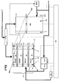
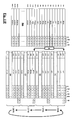
- the memory represented on the figure 1 includes a main area MA, or "area MA”, and an auxiliary memory area XA, or "zone XA".
- the memory zones MA, XA are of the non-volatile type and are erasable and electrically programmable. They are here of the page-FLASH type, that is to say divided into individually erasable or erasable pages by groups of pages selected individually. Each page is divided into segments that can be written individually and provided to each receive a binary word (e.g., a byte).
- the MA field contains target pages and XA contains auxiliary pages.
- the XA field is used to update target pages, without having to delete these pages beforehand.
- the data of the page, after updating are written in the area XA.
- the updating of the data of the page is carried out in a PBUF page buffer: the content of the target page P (i) is copied into the page buffer PBUF, then the one or more new W words are inserted into the page buffer (the old words being overwritten).
- the updated content of the page buffer is then written to an erased page of the XA area, or landing page, and the target page is disabled.
- An auxiliary page can be updated in the same way, if the corresponding target page in the MA field is invalid.
- the content of the auxiliary page is in this case placed in the buffer PBUF, is updated there, and is then written in another auxiliary page, being in the erased state.
- the initial auxiliary page is then disabled.
- Target area test Updating a source page by transferring its data to an auxiliary page may, however, not be necessary if the target area, that is, the segment of the source page to receive new data, is in the erased state. This point will be developed further ("target area test").
- the target pages are selected using RAD addresses and the auxiliary pages are selected using XAD addresses.
- the MA zone has for example an address field ranging from 0 to M-1.
- the target pages and the auxiliary pages each include a data field DT.
- the auxiliary pages further comprise an AF address field. This address field receives the address of the target pages to which the auxiliary pages are associated, and makes it possible to write in the zone XA the updated content of a target page while retaining information linking the target page. and the auxiliary page, and ensuring the traceability of the content transfer.
- the auxiliary page differs from the target page in that it contains the address ⁇ i> of the target page in its AF address field and in that it contains updated data.
- a physical address auxiliary page ⁇ j> (electrical address) containing the address ⁇ i> in its address field is a page d address ⁇ i>.
- two or more auxiliary pages may have the same ⁇ i> address as a target page.
- the ⁇ i> address is a virtual address for an auxiliary page and a physical address for a target page.
- a valid address table or VAM table (“Valid Address Map") is provided to link the RAD addresses of target pages that have been updated in the XA zone, and the XAD physical addresses of the corresponding pages of the zone.
- XA The VAM table is a lookup table that receives applied RAD addresses to the MA area and automatically converts them to XAD addresses.
- the VAM table only includes XAD addresses corresponding to valid auxiliary pages, the addresses of the invalid auxiliary pages being deleted in real time in the table, so that at each XAD address present in the table VAM corresponds a RAD address and a alone. However, at each RAD address present in the table does not necessarily correspond to an XAD address, if the RAD address target page is valid.
- the target pages and the auxiliary pages also comprise a control field F.
- a page P (i) of address i in the area MA comprises a data field DT (i) and a control field F (i)
- a virtual address page P (i) i in the area XA comprises an address field AF (i) containing the physical address ⁇ i>, a data field DT ( i) and a control field F (i).
- the F control fields in the MA and XA fields are used to validate or invalidate the pages, by having two pages of the same ⁇ i> address of the MA area and the XA area, or two pages of same ⁇ i> address in zone XA, are not valid at the same time.
- valid data DT (i) is in an auxiliary page P (i) instead of being in the target page P (i) of address ⁇ i>, the target page is invalid while the auxiliary page is validated.
- two auxiliary pages have the same address ⁇ i> in their address field and are thus attached to the same target page, only one page out of the three can be valid.
- Control fields are also used here to differentiate between a fully erased page and a valid page that has received data.
- the MER flag indicates that the corresponding target page (page indicated by the address field of the auxiliary page considered) is erased or is being erased.
- the flags CS, COK and IS are designed to protect the memory against the consequences of an untimely power failure.
- the CS flag is set to 0 at the beginning of a write step and the COK flag is set to 0 at the end of the write step.
- the IS flag is set to 0 at the beginning of an invalidation step and the IOK flag is set to 0 at the end of the invalidation step. In an application where the supply voltage is not susceptible to inadvertent power failure, the IOK flag will be sufficient to define the status of a page.
- a deleted target page for example the address page ⁇ 8> in figure 2 , contains only bits at 1 in its data field DT ("All 1") and contains only check flags at 1, which means that it is available.
- an erased auxiliary page has only 1 (“All 1") bits in its AF address field and in its DT data field and only has control flags at 1, which also means that it is available and is not attached to any target page.
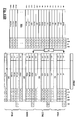
- the zone XA is divided into four sectors S1, S2, S3, S4 of the same size, each comprising N pages, as shown in FIGS. figures 1 and 2 .
- Each sector is addressable over its entire address range, ranging from 0 to N-1.
- Each of the sectors S1 to S4 is in turn assigned a particular status which is indicated by a field SID ("sector identifier") encoded here on two bits.
- the bits of the field SID of each sector are here recorded in a service page SP, or page "not useful" (ie not used to store user data), for example the first page of each sector.
- This page is not included in the address field from 0 to N-1 and is accessible by means of a particular cabling or a dedicated address (on figures 2 , 8A to 11F the SID field is represented in the extension of the first page of each sector, for the sake of simplification of the figures).
- the coding of the UNA status is irrelevant ("xx") because the assignment in turn of each of the statuses to each of the sectors is done in a loop in the order represented on the figure 5 namely, UNA, CUR, ERM, CTM, etc., so that there are still three successive sectors CUR, ERM, CTM, the sector UNA being the contiguous sector following the sector CTM and preceding the sector CUR.
- Each sector S1, S2, S3, S4 thus passes from UNA status to CUR status, then from CUR status to ERM status, then from ERM status to CTM status, then from CTM status to UNA status, and so on.
- S1 is the UNA sector
- S2 is the CTM sector
- S3 is the ERM sector
- S4 is the CUR sector.
- the sector having the UNA status is a sector that is erased during a deletion step according to the invention.
- This step includes the simultaneous deletion of auxiliary pages of the UNA sector and invalid target pages whose addresses are stored in an address table to be erased, or table EAM ("Erase Address Map").
- table EAM Erase Address Map
- memory space is released in the MA area and memory space is released in the XA area.
- the UNA sector is unavailable for both receiving data and providing data. It only includes pages that were previously invalidated before the UNA status was assigned to it. The page addresses of the UNA sector are therefore not included in the VAM table.
- the UNA sector is assigned the CUR status in a step called "rotation of sectors', it being specified that sectors S1 to S4 are immutable and that only the status assigned to them is subject to the abovementioned rotation.
- the sector having the status CUR is the only sector of the zone XA used to write updated page data.
- the landing page is always a CUR sector page.
- the CUR sector can also contain a page to update (source page).
- source page the data of the source page, after updating in the PBUF page buffer, is written in another page of the same sector, then the source page is disabled and its physical address is replaced in the VAM table by the physical address of the other page.
- the valid pages of the CUR sector correspond to deleted or erased target pages, or to invalidated target pages.
- the CUR sector is given the ERM status during the sector rotation step.
- the sector with ERM status has a dual function.
- its address field points to target pages that are to be erased or being erased.
- These addresses are stored in the EAM table at the beginning of the erase step (after the sector rotation step) by reading all the addresses present in the address field of the valid pages of the ERM sector.
- the EAM table receives only page addresses designated by valid pages of the ERM sector and whose MER flag is not equal to 0 (the MER flag being provided to avoid unnecessarily erasing pages that are already erased). .
- the invalid pages of the ERM sector are not taken into account to designate the pages of the MA area to be erased.
- the ERM sector also has the function of saving data that its valid pages contain, while the corresponding pages in the MA area, to which they point, are being erased.
- the ERM sector may contain a page to be updated (source page).
- the source page after update, is written in a CUR sector page, the source page in the ERM sector is invalidated and its address is replaced in the VAM table by the physical address of the page in the CUR sector.
- the sector having the status CTM contains pages that are to be transferred in the zone MA if these pages are valid. All valid CTM pages point to deleted pages in the MA area, since the CTM sector previously had ERM status.
- the page is disabled and the address it contains is removed from the VAM table.
- the CTM sector is unavailable to receive data but may contain a page to update (page that has not yet been transferred to the MA field).
- the page data after updating, is written to a CUR sector page, the source page in the CTM sector is disabled and the address it contains is removed from the VAM table.
- the MER flag on the landing page is set to 0 to indicate that the corresponding page in the MA area has been completely erased.
- the source page after being disabled, is not transferred to the MA field.
- the CTM sector contains only invalid pages and is assigned the UNA sector status during the sector rotation stage.
- the page erasure step can conventionally comprise the application of pulses of a high erase voltage (typically 10 to 15 V) to the memory cells concerned, whereas the memory cells of the pages of the MA area do not have to not be erased receive an erase inhibition voltage.
- a high erase voltage typically 10 to 15 V
- the memory cells of the pages of the MA area do not have to not be erased receive an erase inhibition voltage.
- the zone XA formation of the sectors on different substrates makes it possible to isolate the sectors CTM, ERM, CUR from the erase voltage applied to the sector UNA. Nevertheless, it could be planned to make the four sectors on the same substrate, sectors S1 to S4 then being logical sectors and not physical sectors.
- the erasure step is a partial erase step and several partial erase steps are necessary to obtain the complete erasure of the UNA sector and the MA area pages designated by the ERM sector.
- the number of partial erasure steps to obtain the complete erasure of memory cells is at most equal to the number N of pages. of the sector CUR, the optimum value being N partial erasure steps.
- Each partial erasure step is an erase step in itself conventional but of shorter duration than that of a conventional erase step, and more particularly of duration equal to T / N if T is the average duration of a step complete erasure.
- the partial erasure step according to the invention is thus applied for a duration T / N to the pages of the sector UNA and to the pages of the zone MA designated by the address field of the valid pages of the sector ERM whose flag MER is not 0. If the erasure is performed by pulses (commonly used technique to erase flash memories), the number of erase pulses applied to the memory cells during a partial erase step is equal to P / N if P is the average number of erase high voltage pulses to obtain a complete erasure of the memory cells.
- the partial erase steps can be controlled as is a conventional erase step and may include, in this case, a step of controlling the level of electrical charges in the memory cells (consisting of reading the memory cells with a voltage intermediate reading) in order to stop the application of erase pulses when this is no longer necessary.
- the last partial erase step may comprise less than P / N pulses if the control step shows that there is no need to further erase the memory cells.
- the pages of the MA zone and the XA zone are not completely erased until after N partial erase cycles, ie after N pages of the CUR sector have been written, which then needs to trigger the sector rotation step.
- the former fully cleared UNA sector is used as the CUR sector.
- the pointer progresses from 0 to N-1 and is incremented by one unit at each write-erase cycle. It is reset at each stage of sector rotation.
- the EAM table, the VAM table, the PT address pointer as well as the PBUF page buffer are controlled by a CU control unit with wired logic (state machine) or microprocessor.
- the writing method according to the invention is implemented in the form of an algorithm executed by the unit CU.
- the figure 6 represents a detailed embodiment of the diagram of the figure 1 .
- the memory comprises elements described below.
- the memory includes an IOBUF input / output buffer connected to an IOT input / output terminal. This buffer allows the memory to receive CMD read or write commands accompanied by AD word addresses, the writing commands being also accompanied by one or more W words to be written.
- the address of a word AD includes a RAD address (most significant address bits) and a CAD column address (least significant address bits).
- the RAD line address is the address of a target page in the MA field and the CAD column address is the address of the segment where the word is located in the target page or in the corresponding source page.
- An ADB address bus carries RAD page addresses that are read in the auxiliary pages or that accompany commands, as well as CAD column addresses accompanying commands.
- a line decoder RDEC1 makes it possible to select pages in the MA zone for reading, writing or erasure, and a column decoder CDEC1 makes it possible to select words to be read or written in selected pages of the zone MA.
- a PRCT1 circuit reads and writes the MA area and includes read amplifiers and programming latches (not shown) for reading or writing a selected word in a page.
- a line decoder RDEC2 makes it possible to select pages in the XA zone for reading or writing, and a column decoder CDEC2 for selecting words to be read or written in selected pages of zone XA.
- a PRCT2 circuit provides for writing and reading the XA area and includes read amplifiers and programming locks for reading or writing at least one word or the address field of a selected page.
- the circuits PRCT1, PRCT2 are configured to allow the control unit CU to read or write the flags CS, COK, IS, IOK (MA or XA area pages), MER (XA area pages) and as the SID field (service pages in area XA).
- the flags are read automatically by additional amplifiers provided for this purpose and are sent to the control unit.
- specific programming locks allow the control unit to individually change the value of each flag.
- the decoder RDEC2 comprises four decoding stages SS1, SS2, SS3, SS4 and receives, via an MX2 multiplexer, an XAD1 page address provided by the VAM table or an XAD2 page address provided by the pointer PT. These addresses are valid for reading and writing only.
- the pages of the sector to be erased are selected by the decoder RDEC2 on receipt of an ERSi signal which can have four values ESR1, ESR2, ESR3, ERS4, or a value per sector to be selected in erasure.
- the application of the ERSi signal inhibits the selection of pages by means of the XAD1 or XAD2 addresses.
- the pointer PT comprises a volatile type counter CPT1 and a circuit SH of concatenation of high-order and low-order address bits, also forming an output buffer of the pointer PT.
- the XAD2 address provided by the pointer PT is the result of the concatenation of an XAD0 address provided by the counter CPT1 and a most significant address, forming a sector address SAD, provided by the signal unit.
- CU control the two addresses being applied to the circuit SH.
- the address XAD0 is thus a page address within the selected sector and goes from 0 to N-1.
- the control unit can select pages of the same low-order address in the CTM and CUR sectors, by changing only the sector address SAD.
- control unit After a sector rotation step, the control unit sets the counter CPT1 to 0 so that the pointer provides the address of the first current page of the CTM sector to be transferred in the MA area (if this page is valid) or the address of the current first page erased from the CUR sector to receive updated data, according to the SAD area address applied to it. The control unit then increments the counter by means of an INCR signal, at each subsequent write-erase cycle.
- the pointer PT is also used by the control unit to load in the EAM table the page addresses to be erased in the MA area.
- the counter CPT1 is set to 0 and the sector ERM is selected for reading.
- the address fields of the sector pages are read and transferred to the EAM table. Since the control fields of the pages are automatically read by the PRCT2 circuit, the control unit only loads in the EAM table the addresses read in valid pages and whose MER flag is not equal to 0.
- the VAM table is managed in a volatile register REG1 which comprises a clocking input connected to the address bus ADB to receive the RAD address present on the bus, and an output connected to the decoder RDEC2 via the multiplexer MX2.
- REG1 register contains a prerecorded RAD address list and, opposite this list, an XAD address list which is initially empty, the set forming the VAM table.
- At a RAD address in the table is a location to receive an XAD address. When a RAD address is on the bus and is seen by the pointing entry, the register is automatically set to that address in the table and provides the corresponding XAD address (designated XAD1 on the figure 6 ) if the location is not empty.
- the register then sets an INX signal to indicate to the control unit that a valid page of RAD address is in the area XA. If the location in front of the RAD address is empty in the VAM table, the signal INX remains at 0. This signal thus enables the control unit to know which reading circuit PRCT1, PRCT2 it must activate.
- the REG1 register also includes a LIN loading input which receives the XAD2 address provided by the pointer PT.
- the control unit wants to associate a given address XAD2 provided by the pointer PT with a given address RAD present on the bus ADB, the control unit applies a loading signal LD1 to the register REG1 and the address present on the LIN entry is stored in the VAM table, opposite the RAD address selected by the pointing entry.
- the control unit wants to delete an XAD address in the VAM table, it applies an erase signal DEL to the register.
- the page buffer here comprises two PBUFA, PBUFB buffers, the pages being updated by the PBUFB buffer.
- the PBUFA buffer comprises an input I1 connected to outputs of the circuits PRCT1, PRCT2 via an MX1 multiplexer, to receive a word read in one of the zones MA, XA, or an entire page read word by word, as well as the field d address of an auxiliary page.
- the buffer PBUFA emits an ER signal when a word loaded in the buffer has all its bits equal to 1 (erased word). This signal is also set to 1 when all the words of a page have been loaded into the PBUFA buffer and the page contains only 1-bit (erased page).
- the signal ER is for example the result of the AND function of all the bits present in the PBUFA buffer, which are set to 1 by default after resetting the buffer.
- the buffer PBUFA also comprises an output O1 connected to inputs of the circuits PRCT1, PRCT2 via the multiplexer MX1, to load in the circuits PRCT1, PRCT2 a write word in the areas MA, XA, or to load in the circuit PRCT2 a field of address to write in the XA field. It also comprises an input / output IO2 connected to an input / output I / O of the buffer PBUFB, to transfer its contents in this second buffer or to receive the contents of this second buffer.
- the PBUFA buffer also comprises an input / output IO3 connected to the VAM table and the address bus ADB, to provide RAD addresses read in auxiliary page address fields or to load into the buffer a present address. on the bus and to be written in the address field of an auxiliary page.
- the buffer PBUFB comprises a second input I2 connected to the buffer IOBUF to receive one or more words W to be written in the memory.
- the buffer PBUFB updates the content of a page provided by the PBUFA buffer by inserting the word or words provided by the IOBUF buffer, its input / output IO2 to relocate in the buffer PBUFA updated page data.
- the EAM table is managed by a volatile register REG2 having an input connected to the input / output IO3 of the buffer PBUFA, to receive addresses of pages to be erased read in the sector ERM, in response to a loading signal LD2 emitted by the control unit.
- An output of the register REG2 is applied to an address input of the decoder RDEC1 via an MX3 multiplexer whose other input is connected to the address bus.
- the control unit uses the MX3 multiplexer to apply to the RDEC1 decoder the RAD address present on the bus.
- erase mode the control unit connects the output of the register REG2 to the decoder RDEC1.
- the RDEC decoder 1 includes word line locks (not shown) for selecting pages whose addresses are in the EAM table. For this purpose the register REG2 is read address after address. At each address read, the control unit applies to the decoder RDEC1 a signal S / R (Set / Reset) to lock the selection of the corresponding page. Once all the pages designated by the EAM table are selected, the erase voltage can be applied to them collectively, the unselected pages receiving an erase inhibition voltage.
- the CAD column address provided by the IOBUF buffer is applied to the decoders CDEC1, CDEC2 via an MX4 multiplexer whose other input is connected to the output of an address counter CPT2.
- the control unit applies the CAD address to the decoders CDEC1, CDEC2 and activates one of these decoders.
- the control unit connects the output of the counter CPT2 to the decoders CDEC1, CDEC2, sets the counter to 0 and scans the entire column address field to read the words one after the other , the result of the reading being loaded into the PBUFA buffer.
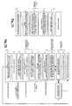
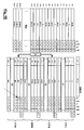
- the organization chart Figure 7A describes an initialization cycle of the memory after it is powered on, which follows a voluntary or accidental power off.
- the VAM and EAM tables, as well as the PT pointer being volatile data, their content is regenerated by the control unit from the information in the areas MA and XA. We distinguish the following stages.
- the control unit reads the SID fields in the service pages and identifies the UNA, CTM, ERM, CUR sectors. As indicated above, the UNA sector is identified by default as being the fourth sector following the sectors successively presenting SID equal to 11, 01 and 00 (Cf. Fig. 5 ).
- This step is identical to that performed after a rotation of sectors.
- the address fields are read in the ERM sector and are loaded in the REG2 register via the PBUFA buffer, if they belong to valid pages and if the MER flag of these pages is not 0. After a cut of power supply, a complete erase cycle is applied by security to the pages designated by the ERM sector.
- the control unit must find here the first page cleared from the CUR sector. To find this first page after a power failure, the counter CPT1 is set to zero by means of the signal RST and the sector CUR is read page by page by incrementing the counter until an erased page is found. The low-order address of this page is then left in the counter CPT1 to generate the XAD2 address provided by the pointer PT. It should be noted that a page of the CUR sector is considered not to be in the erased state since the flag CS is equal to 0 and even if the flag COK is to 1. This means that the page began to be written before the power cut.
- the memory is protected against accidental power cuts thanks to the CS / COK and IS / IOK flag redundancies which allow to trace step by step intermediate processing steps such as the beginning of the writing of a page and the end of the process. writing of the page, or the beginning of the invalidation of a page and the end of the invalidation of the page, so that when the power is turned on the processing unit can unambiguously identify the valid pages and invalid pages, unfinished processes and potential conflicts.
- the consistency check is based on an analysis of the inconsistencies between the flags. For example, if a page was being written at the time of the break the page has the flag CS at 0 but the flag COK is at 1.
- the data of the page are therefore not valid and the control unit looks for the invalid page of the same address (physical or virtual) in order to find the old data on the page, so that only the update has been lost.
- Various consistency check steps and corresponding corrective actions may be provided and will not be described here for the sake of simplicity.
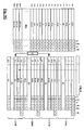
- the Figure 7B is a flowchart describing an exemplary embodiment of the write method according to the invention, in response to a command to write a word W in a page P (i) of address ⁇ i>.
- the method comprises a step of testing the target area (segment of the source page to receive the word), a step of updating the page data, and the write-erase cycle according to the invention.
- the target zone test is intended to avoid engaging the write-erase cycle if the target area is in the erased state, which may be the case when the target page is completely erased or when data has been deleted. written in other segments of the targeted page but not in the target area itself.
- the content of the target area is read at the address indicated by the command (step 20).
- the target area may be in the MA area (the source page is the target page) or in the XA area (the source page is different from the target page).
- the selection of the appropriate zone MA or XA is done automatically by the VAM table and the signal INX indicates to the control unit which reading circuit it must activate.
- the control unit then examines the ER signal provided by the PBUFA buffer (step 21). If this signal equals 1, the control unit writes the word in the target zone (step 22) and then returns to a step of waiting for a new command. If the ER signal is equal to 0, this means that the target zone is not erased and can not be written. The control unit then proceeds to the step of updating the page data, described below.
- All words contained in the source page are loaded into the PBUFA buffer, using the CPT2 counter to scan the CAD column addresses.
- the address of the target page present on the address bus is also loaded into the PBUFA buffer.
- the buffer thus includes an initial set of data and the address of the target page.
- the contents of the PBUFA buffer are transferred to the PBUFB buffer. The latter incorporates the word to write and overwrites the initial word (step 30) without modifying the other words of the page.
- the write-erase cycle according to the invention comprises the three steps described above, and management steps of the pointer PT.
- Step 32 The control unit applies a partial erasure step to the UNA sector and to the pages of the MA area listed in the EAM table, after having transferred in the decoder RDEC1 the addresses present in the EAM table and locked the selection of the corresponding pages.
- Step 34 The control unit must transfer in the MA zone the data present in a page of the CTM sector designated by the pointer PT. For this purpose, the control unit applies to the pointer PT a sector address SAD corresponding to the sector CTM and first analyzes the control field of the page to determine if it is valid.
- the control unit sets all page data to 0 including flags and address field. This zeroing of the invalid page data is optional and is only provided in connection with the management of electric charge levels in certain types of memory cells, so that the erase process is applied to memory cells. finding in the same electrical state. If the page is not valid and contains only data equal to 0, the control unit has no operation to perform on this page.
- the page is read using the PRCT2 circuit and is copied to the PBUFA buffer (while the updated page data is stored in the PBUFB buffer).
- the address field present in the page is applied to the line decoder CDEC1 via the buffer PBUFA, the address bus and the multiplexer MX3.
- the contents of the buffer PBUFA is then transferred to the circuit PRCT1 and is written in the relevant page of the zone MA.
- the CS flag of the page is set to 0 before writing the words and the COK flag is set to 0 after writing the words.
- Step 36 After it has been transferred to the MA area, the page of the CTM sector designated by the pointer PT is disabled and its physical address is removed from the VAM table. For this purpose, the flag IS of the page is set to 0, then all the data of the page of the sector CTM are set to 0 (management of the levels of electric charges) except the flags IOK and MER, which are set to 0 last location. Here too this zeroing is optional and is only foreseen in relation to the management of the levels of electrical charges.
- Step 38 This step is to increment the PT pointer.
- the control unit first determines whether the address XAD0 supplied by the counter CPT1, which represents the LSB bits (PT) of the address supplied by the pointer, is equal to N-1, ie the maximum value of the address field in each sector. If the maximum address N-1 is reached the control unit resets the counter CPT1 to 0 otherwise it increments it by one unit by means of the signal INCR. The value of the incremented counter remains an internal value of the counter and is not unlocked by the buffer SH.
- Step 40 The updated page data present in the PBUFB buffer is transferred to the PBUFA buffer.
- the sector address SAD applied to the pointer is modified by the control unit to address the sector CUR.
- the pointer PT now supplies the address of a page erased in the sector CUR (having the same low-weight address as the page of the CTM sector object of steps 34 and 36).
- the RAD address of the target page is again placed on the ADB bus, via the input / output IO3 of the buffer PBUFA.
- the contents of the buffer PBUFA is transferred into the circuit PRCT2 and is written in the selected page.
- the CS flag of the page is set to 0 beforehand and the COK flag is set to 0 after writing the page.
- the MER flag is also set to zero if the source page whose data has been loaded into the page buffer (step 30) belongs to the CTM sector or to the ERM sector, since the pages of the CTM sector are attached to deleted target pages and ERM sector pages are attached to target pages being erased.
- Step 42 The source page is again selected to be disabled, the output of the VAM table (XAD1 address) being applied to the RDEC2 decoder via the MX2 multiplexer.
- the IS flag of the page is set to 0, then all data on the CTM area page is set to 0 (electric charge level management) except the IOK and MER flags, which are set to 0 last. If the source page belongs to the ERM sector, only the IS flag is set to 0. Indeed, the page contains the address of a page of the MA sector being erased. This address can not be erased until the erase step is complete because it is necessary to regenerate the EAM table after a power failure.
- the XAD address of the source page is removed from the VAM table (LED signal).
- the address of the new source page provided by the pointer PT (address XAD1) is stored in the table VAM by means of the signal LD1 applied to the register REG1.
- Step 44 During this step, the SID sector identifiers are modified by the control unit to rotate the sectors, if the pointer has been set to 0 in step 38.
- step 44 the control unit returns to the initial state of waiting for a new command.
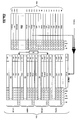
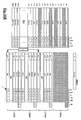
- the Figures 8A to 8H illustrate the case where the source page of the write-erase cycle is the target page targeted by write command (which means that the source page is in the MA field).
- FIG 8A The memory receives a write command of a word W targeting the target page P (12).
- Its content DT (12) is copied into the page buffer PBUF (PBUFA, PBUFB).
- the new word W is inserted therein to obtain updated page data DT '(12).
- Figure 8B A partial erase step is applied to the UNA sector pages as well as to the MA area pages whose ⁇ 1>, ⁇ 4>, ⁇ 6>, ⁇ 10> addresses are present in the address fields. valid pages of the ERM sector whose MER flag is not equal to 0, and were previously copied into the EAM table. This is the first step of partial erasure after rotation of the sectors and the pointer PT is positioned on the first page of the sector CTM or on the first page of the sector CUR (according to the address of sector SAD which is applied to it ), which means that the low-order address XAD0 is equal to 0 in the counter CPT1 ( Fig. 6 ).
- the address pages ⁇ 1>, ⁇ 4>, ⁇ 6>, ⁇ 10> contain data which are all 0 (All 0, Fig. 8A ) and flags that are also 0, because these pages were previously invalidated. These data and flags are in an indeterminate state "x" after the partial erase step, the indeterminate state corresponding to a distribution of electrical charges in the memory cells that does not correspond to the logical "0" or “1” logic, the logic "1" or erase logic value can be reached only after N partial erase steps.
- Figure 8C the CTM address (high-order address SAD) is applied to the pointer PT, the output buffer SH ( Fig. 6 ) is unlocked and the pointer points to the first page of the CTM area.
- the address field of this page includes the address ⁇ 9> (virtual address of the page).
- the data on this page is transferred to the physical address page ⁇ 9> of the MA area.
- the copy step includes setting the CS flag of the physical address page ⁇ 9> to 0, and then copying the words from the virtual address page ⁇ 9> to the physical address page ⁇ 9>. , then set the COK flag of the physical address page ⁇ 9> to 0.
- Figure 8D the virtual address page ⁇ 9> of the CTM sector is invalidated by successively setting the IS flag to 0, then the data and address fields of the page, then the IOK and MER flags. The physical address of this page is removed from the VAM table.
- Figure 8E The control unit applies to the pointer PT the address of the sector CUR, the output buffer SH is unlocked and the pointer now designates the deleted page of the sector CUR to receive the updated page data, here the first page of the CUR sector.
- the CS flag of the page is set to 0.
- Figure 8F the pointer PT is incremented by applying the signal INCR to the counter CPT1 ( Fig. 6 ) but the new pointer address remains blocked by the SH buffer. The pointer is thus positioned on the following address but this address is not validated at the input of the decoder RDEC2 and the register REG1 of the table VAM.
- Figure 8G the updated page data DT '(12) present in the buffer PBUF, as well as the address ⁇ 12> of the target page, are written in the deleted page of the sector CUR (the pointer continuing to provide the address of this page).
- the writing is done in the following order: writing of the data and the address field ⁇ 12> then setting to 0 of the flag COK. This page therefore becomes a virtual address source page ⁇ 12> but will not be saved in the VAM table until the source page is invalidated.
- Figure 8H the address source page ⁇ 12>, which is also the target page here, is disabled: setting the IS bit to 0, setting all page data to 0, setting the IOK bit to 0.
- the physical address of the virtual address page ⁇ 12> provided by the pointer PT is then stored in the VAM table.
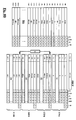
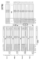
- FIGS. 9A to 9H illustrate the write-erase cycle in the case where the source page is in the CTM sector, which means that the data of the corresponding target page has already been transferred to the source page during a previous update.
- FIG 9A The memory receives a write command of a word W targeting the target page P (3).
- the target page is in the erased state ("All 1", all of its bits are at 1) and the VAM table designates a source page in the virtual address CTM sector ⁇ 3>.
- the DT (3) content of the source page is copied to the PBUF page buffer.
- the new word W is inserted therein to obtain updated page data DT '(3).
- Figure 9B A new partial erase step is applied to the pages of the UNA sector and the pages of the MA area with ⁇ 1>, ⁇ 4>, ⁇ 6>, ⁇ 10> addresses. This is the second partial erase step and the pointer PT is positioned on the second page of the CTM sector or on the second page of the sector CUR (according to the sector address SAD applied to it).
- the address pages ⁇ 1>, ⁇ 4>, ⁇ 6>, ⁇ 10> always contain data that is in an indeterminate state "x".
- FIG. 9C The CTM sector address is applied to the PT pointer, the SH output buffer is unlocked, and the pointer points to the second page of the CTM sector.
- the data on this page is transferred to the physical address page ⁇ M-2> of the MA zone and the CS and COK flags of the MA zone are set to zero.
- Figure 9D the virtual address page ⁇ M-2> of the CTM sector is invalidated by successively setting the IS flag to 0, then the data and address fields of the page, then the IOK and MER flags. The physical address of this page is removed from the VAM table.
- Figure 9E The control unit applies to the pointer PT the address of the sector CUR, the output buffer SH is unlocked and the pointer now designates the deleted page of the sector CUR to receive the updated page data, here the second page of the CUR sector.
- the CS flag of the page is set to 0.
- Figure 9F the pointer PT is incremented by applying the signal INCR to the counter CPT1 ( Fig. 6 ) but the SH buffer is not unlocked.
- Figure 9G the updated page data DT '(3) present in the buffer PBUF, as well as the address ⁇ 3> of the target page, are written in the deleted page of the sector CUR.
- the COK flag is set to 0.
- the MER flag is also set to 0 because the source page belongs to the CTM sector and is thus attached to an erased page of the MA area.
- the landing page in the CUR sector thus becomes a virtual address page ⁇ 3> but will not be recorded in the VAM table until the source page is invalidated.
- FIG. 9H The virtual address source page ⁇ 3>, whose physical address is provided by the VAM table, is disabled: setting the IS bit to 0, setting all page data to 0, setting the IOK bit to 0 . Its physical address is then removed from the VAM table. The physical address of the new virtual address page ⁇ 3> provided by the pointer PT is stored in the VAM table. Note that the switch from one page to another for the operations just described is performed using the MX2 multiplexer ( Fig. 6 ) which alternately passes an auxiliary page address provided by the VAM table to an auxiliary page address provided by the pointer PT.
- FIGS 10A to 10C illustrate the write-erase cycle in case the source page is in the ERM area.
- FIG. 10A The memory receives a command to write a word W for the target page P (10).
- the target page is being erased (all bits are at the indeterminate "x" value) and the VAM table refers to the virtual address source page ⁇ 10> in the ERM area.
- the DT (10) content of the source page is copied to the PBUF page buffer.
- the new word W is inserted therein to obtain updated page data DT '(10).
- Figure 10B several steps are represented grouped in this figure.
- a new partial erase step is applied to the UNA pages and to the MA pages of ⁇ 1>, ⁇ 4>, ⁇ 6>, ⁇ 10> addresses.
- the CTM sector address is then applied to the PT pointer, the output buffer SH is unlocked, and the pointer points to the third page of the CTM sector.
- the address field of this page includes the address ⁇ 13>.
- the data on this page is transferred to the physical address page ⁇ 13> of the MA area.
- the CS and COK flags on this page are set to zero.
- the virtual address page ⁇ 13> of the CTM sector is then invalidated by successively setting the IS flag to 0, then the data and address fields of the page, then the IOK and MER flags.
- the physical address of this page is removed from the VAM table.
- the control unit then applies to the pointer PT the address of the sector CUR, the output buffer SH is unlocked and the pointer indicates the deleted page of the sector CUR to receive the updated page data, here the third page of the sector CUR.
- the CS flag of the page is set to 0.
- the internal value of the PT pointer is incremented.
- the updated page data DT '(10) in the buffer PBUF, as well as the address ⁇ 10> of the target page are written in the deleted page of the sector CUR.
- the COK flag is set to 0.
- the MER flag is also set to 0 here because the virtual address source page ⁇ 10> is in the ERM sector and the corresponding physical address page ⁇ 10> is in progress. erasure. The MER flag thus indicates that it will not be necessary to delete the corresponding page in the MA zone when the sector CUR will have the status of sector ERM (after the sector rotation step).
- FIG. 10C The virtual address source page ⁇ 10> is disabled by setting the IS bit to 0. However, the rest of the page is not set to 0 because this page belongs to the ERM sector and its address field may be necessary to regenerate the EAM table in case of power failure. Its physical address is, however, removed from the VAM table. The address of the new virtual address page ⁇ 10> is stored in the VAM table.
- the Figures 11A to 11F illustrate the write-erase cycle in case the source page is in the CUR sector.
- FIG 11A The memory receives a write command of a word W targeting the target page P (3).
- the target page is in the erased state and the VAM table designates a virtual address page ⁇ 3> in the CUR sector which is thus used as the source page.
- This page has been updated recently ( Fig. 9G ). Its content DT '(3) is copied into the page buffer PBUF. The new word W is inserted therein to obtain updated page data DT '' (3).
- Figure 11D the updated page data DT "(3) present in the buffer PBUF, as well as the address ⁇ 3> of the target page, are written in the deleted page of the sector CUR (the pointer continuing to provide the address the SH flag is set to 0.
- the MER flag is also set to 0 because the MER flag of the source page is equal to 0. It can be seen that the corresponding page in the MA field, physical address ⁇ 3> is now cleared.
- Figure 11E the virtual address source page ⁇ 3> is disabled: setting the IS bit to 0, setting all page data to 0, setting the IOK bit to 0. Its physical address is removed from the VAM table. The physical address of the new virtual address page ⁇ 3> provided by the pointer PT is stored in the VAM table.
- Figure 11F Sector rotation is performed by modifying the SID fields S3 and S4 sectors.
- the second bit of the SID field of the sector S3 is set to 0 and the first bit of the field SID of the sector S4 is set to 0.
- the sectors S1, S2, S3 and S4 become respectively sectors CUR, UNA, CTM and ERM.
- aspects of the invention can be implemented independently of each other, depending on the desired objectives and applications.
- the aspects of the invention relating to the protection against tearing are not required in an application where there is no risk of inadvertent power failure.
- the aspects of the invention relating to the prediction of the four sectors of the auxiliary zone XA are advantageous for ensuring the reception of an uninterrupted flow of instructions, but the zone XA could also comprise only two sectors CUR, CTM.
- the deletion of the CTM sector and the pages of the area MA attached to the pages of the sector CUR would be ensured during a resting step following the reception of N write commands, the sector CTM then becoming sector CUR and the CUR sector becoming CTM sector.
- the address fields in the auxiliary pages would not be needed if a nonvolatile VAM table was used.
- the order of the steps of the write-erase cycle described above can be modified, for example by performing the transfer of the pages of the CTM sector before the partial erasure step, or the partial erasure step after writing the updated page data in the landing page, etc. Generally speaking, it is within the abilities of those skilled in the art to design various variants and embodiments implementing any or part of the aspects of the invention.
- the invention has been implemented in a page-FLASH memory, that is to say a memory divided into pages in which the pages are erasable individually or in groups of pages selected individually, and wherein each page is divided into individually writable segments provided to each receive a binary word.
- this embodiment is not limiting and that the method according to the invention can be implemented by for example, in a memory where the data is written per page instead of written by word (in which case the writing granularity is chosen equal to the erasure granularity). In this case, the step of testing the target area is no longer necessary or the step of preparing the updated page data, since the data of each new page must overwrite all the page data. previously saved.
- page should not be construed as designating a set of memory cells connected to the same word line controlled by a line decoder.
- the term “page” generally refers to a location that is individually erasable and includes a plurality of memory cells. This location may or may not be divided into individually writable segments.
- the word "sector" as used to designate subdivisions of the memory zone XA does not necessarily designate physical sectors (distinct substrates) but may designate logical sectors, or even parts of a global memory plane including the zones. MA and XA.
- each aspect of the invention described above constitutes in itself an improvement that can be applied without necessarily being combined with the other aspects of the invention.
- the invention allows the realization of embedded memories and in particular memories embedded in integrated circuits for smart cards or electronic tags.
- the invention makes it possible to use Flash memories as embedded memories, an application that was previously reserved for EEPROM memories.
- the invention thus includes the production of a smart card or an electronic tag (of the contact or non-contact type RFID or UHF) comprising an integrated circuit equipped with a memory according to the invention.
Abstract
Description
La présente invention concerne les mémoires non volatiles et notamment les mémoires effaçables et programmables électriquement de type FLASH.The present invention relates to non-volatile memories and in particular electrically erasable and programmable memories of FLASH type.
Le marché des mémoires effaçables et programmables électriquement sur microplaquettes de silicium est traditionnellement partagé entre la famille des mémoires EEPROM et celle des mémoires FLASH (ou FLASH-EEPROM).The market for erasable and electrically programmable memories on silicon chips is traditionally shared between the family of EEPROM memories and that of FLASH memories (or FLASH-EEPROM).
Les mémoires EEPROM comprennent des cellules mémoire comportant un transistor à grille flottante et un transistor d'accès. Des transistors de contrôle de grille permettent d'appliquer sélectivement une tension d'effacement à des groupes de cellules mémoire ou mots comprenant un faible nombre de cellules mémoire, par exemple de 8 à 16 cellules mémoire. Elles offrent ainsi une très fine granularité en effacement. Par ailleurs les transistors d'accès isolent les transistors à grille flottante des lignes de bit et permettent de prévoir des tensions de seuil de signes différents entre des cellules mémoire effacées et des cellules mémoire programmées. Ces mémoires sont donc faciles à mettre en oeuvre mais les cellules mémoire occupent une surface importante en raison de leur structure à deux transistors.The EEPROM memories comprise memory cells comprising a floating gate transistor and an access transistor. Gate control transistors are used to selectively apply an erase voltage to groups of memory cells or words comprising a small number of memory cells, for example from 8 to 16 memory cells. They thus offer a very fine granularity in erasure. In addition, the access transistors isolate the floating gate transistors from the bit lines and make it possible to provide threshold voltages of different signs between erased memory cells and programmed memory cells. These memories are therefore easy to implement but the memory cells occupy a large area because of their two transistor structure.
Les mémoires de type FLASH ne comportent qu'un transistor à grille flottante par cellule mémoire et présentent ainsi l'avantage d'une grande compacité en termes de surface de silicium occupée (nombre de cellules mémoire par unité de surface). En contrepartie, l'absence de transistor d'accès nécessite de prévoir des tensions de seuil positives tant pour les cellules mémoire effacées que les cellules mémoire programmées, afin de ne pas créer des courts-circuits sur les lignes de bit. Les oxydes de grille doivent ainsi être épais pour maintenir durablement les charges électriques piégées dans les grilles flottantes, ce qui entraîne une augmentation notable du temps d'effacement. Plus particulièrement, l'effacement des cellules mémoire FLASH est généralement effectué par effet tunnel tandis que leur écriture (programmation) est effectuée par injection d'électrons chauds. Le temps nécessaire à l'écriture des cellules mémoire est court, par exemple 5 microsecondes, tandis que le temps d'effacement est long, par exemple 100 millisecondes. Par ailleurs, la programmation par injection d'électrons chauds entraîne l'apparition d'un fort courant de programmation, de sorte que le nombre de cellules mémoire pouvant être écrites simultanément doit être limité. Ainsi, l'écriture de cellules mémoire est généralement effectuée mot par mot, contrairement aux mémoires EEPROM qui permettent d'écrire simultanément toute une page. Enfin, les mémoires FLASH ne sont effaçables que par secteur, un secteur comprenant des transistors dont les bornes de potentiel bas (bornes de source pour des transistors de type NMOS) sont reliées au même substrat.The FLASH type memories comprise only one floating gate transistor per memory cell and thus have the advantage of a great compactness in terms of occupied silicon area (number of memory cells per unit area). In return, the absence of an access transistor requires the provision of positive threshold voltages for both the erased memory cells and the programmed memory cells, so as not to create short circuits on the bit lines. The gate oxides must thus be thick to sustainably sustain the electrical charges trapped in them. floating grids, resulting in a significant increase in erase time. More particularly, the erasure of the FLASH memory cells is generally effected by tunneling while their writing (programming) is performed by injection of hot electrons. The time required for writing the memory cells is short, for example 5 microseconds, while the erase time is long, for example 100 milliseconds. Furthermore, the programming by hot electron injection results in the appearance of a strong programming current, so that the number of memory cells that can be written simultaneously must be limited. Thus, the writing of memory cells is generally performed word by word, unlike EEPROM memories that allow to simultaneously write a whole page. Finally, the FLASH memories are erasable only by sector, a sector comprising transistors whose low potential terminals (source terminals for NMOS type transistors) are connected to the same substrate.
Les mémoires FLASH ont ainsi été, originellement, dédiées au stockage de masse. Divers perfectionnements furent ensuite proposés afin qu'elles puissent offrir des caractéristiques se rapprochant des mémoires EEPROM, et ce afin d'ouvrir aux mémoires FLASH des domaines d'application originellement réservés aux mémoires EEPROM. De façon générale, le but poursuivi par ces perfectionnements est d'offrir des mémoires FLASH capables de rivaliser avec les mémoires EEPROM en termes de souplesse d'emploi, sans perdre leurs avantages en termes de capacité de stockage par unité de surface de silicium.FLASH memories were originally dedicated to mass storage. Various improvements were then proposed so that they could offer characteristics that are close to the EEPROM memories, in order to open to the FLASH memories application domains originally reserved for the EEPROM memories. In general, the purpose of these improvements is to offer FLASH memories that can compete with EEPROMs in terms of flexibility, without losing their advantages in terms of storage capacity per unit silicon area.
Parmi les perfectionnements ayant permis de faire évoluer le marché des mémoires FLASH, on peut citer :
- la conception d'une mémoire FLASH programmable par page, telle que décrite par le
brevet EP 1 111 621 - la conception d'une mémoire FLASH effaçable par page, telle que décrite par le
brevet EP 1 342 244 - la conception d'une mémoire FLASH programmable par mot et effaçable par page, ou page-FLASH, telle que décrite par le
brevet EP 1 486 986 EP 1 342 244
- the design of a programmable memory FLASH per page, as described by the
patent EP 1 111 621 - the design of an erasable FLASH memory per page, as described by the
patent EP 1 342 244 - the design of a word-programmable and page-erasable FLASH memory, or page-FLASH, as described by the
patent EP 1 486 986 EP 1 342 244
Ce dernier perfectionnement a permis de commercialiser des mémoires FLASH offrant les mêmes fonctionnalités apparentes que des mémoires EEPROM, mais dans lesquelles des limitations subsistent, à savoir:
- le temps d'effacement long, qui peut s'avérer gênant dans certaines applications. En effet le temps apparent d'écriture d'un mot est essentiellement imposé par le temps d'effacement de la page, puisque l'algorithme interne doit effacer la page entière chaque fois qu'un nouveau mot est écrit ;
- une absence de protection contre les coupures intempestives de tension d'alimentation. En effet, si une coupure d'alimentation survient pendant l'effacement de la page cible et tandis que la page mise à jour se trouve encore dans le tampon de page volatile, toutes les données de la page sont irrémédiablement perdues. De ce fait les mémoires FLASH ne peuvent actuellement être utilisées comme mémoires enchâssées ("embedded memories") dans des circuits intégrés destinés à des applications où le risque de coupure d'alimentation électrique est élevé. Il s'agit typiquement des applications aux cartes à puce ou aux étiquettes électroniques, dans lesquelles l'alimentation des circuits intégrés est fournie par un dispositif externe (lecteur) et peut disparaître à tout instant en cas "d'arrachement" (retrait de la carte de la fente du lecteur pour une carte à contact, éloignement brutal de la carte de la bobine du lecteur pour une carte sans contact à couplage inductif, etc.).
- long erasure time, which can be annoying in some applications. Indeed the apparent time of writing a word is essentially imposed by the erasure time of the page, since the internal algorithm must erase the entire page each time a new word is written;
- a lack of protection against unintentional power supply interruptions. Indeed, if a power failure occurs during the deletion of the target page and while the updated page is still in the volatile page buffer, all data on the page are irretrievably lost. As a result, FLASH memories can not currently be used as embedded memories in integrated circuits for applications where the risk of power failure is high. These are typically applications for smart cards or electronic tags, in which the power of the integrated circuits is provided by an external device (reader) and can disappear at any moment in case of "tearing" (removal of the card reader slot for a contact card, abrupt removal of the reader coil card for an inductively coupled contactless card, etc.).
Il peut ainsi être souhaité de perfectionner les mémoires de type FLASH et de façon générale tout type de mémoire non volatile présentant tout ou partie des propriétés précitées, selon au moins l'un des axes de perfectionnement suivants:
- optimiser le temps d'effacement apparent des données ;
- optimiser le temps d'effacement apparent des données sans devoir interrompre un flot d'instructions ;
- protéger des données contre le risque de coupure d'alimentation électrique pendant le processus d'écriture.
- optimize the apparent deletion time of the data;
- optimize the apparent erase time of the data without interrupting a flow of instructions;
- protect data from the risk of power failure during the writing process.
Chacun de ces axes de perfectionnement est visé indépendamment des autres, ou en combinaison avec les autres, selon les applications concernées.Each of these areas of improvement is targeted independently of others, or in combination with others, depending on the applications concerned.
Concernant la protection des données contre les coupures d'alimentation, la demande de brevet
Ce procédé nécessite de gérer une valeur de comptage qui doit nécessairement repasser par zéro, la taille du champ de comptage n'étant pas infinie, de sorte qu'une valeur de comptage récente après remise à zéro peut présenter une valeur inférieure à une valeur de comptage précédente générée avant la remise à zéro. Par ailleurs, si une coupure de tension intervient pendant que la page initiale est en cours d'effacement, les cellules mémoire de la page ne sont pas entièrement effacées. Les données qu'elles contiennent peuvent alors présenter des valeurs erronées, du fait que les charges électriques dans les cellules mémoire sont indéterminées tant que le processus d'effacement n'est pas achevé. Ainsi, après remise sous tension suite à une coupure d'alimentation, une valeur de comptage lue dans des cellules mémoire incomplètement effacées pourrait présenter une valeur arbitraire supérieure à la valeur de comptage présente dans la page dernièrement mise à jour. Dans ces conditions, la page ancienne mal effacée contenant des données invalides pourrait être vue comme la "bonne" page, tandis que la vraie "bonne" page serait effacée.This method requires managing a count value which must necessarily return to zero, the size of the count field not being infinite, so that a recent count value after resetting may have a value less than a value of previous count generated before resetting. In addition, if a power failure occurs while the initial page is being erased, the memory cells of the page are not completely erased. The data they contain may then have erroneous values because the electrical charges in the memory cells are undetermined until the erase process is complete. Thus, after power-up following a power failure, a count value read in incompletely erased memory cells could have an arbitrary value greater than the count value present in the page last updated. Under these conditions, the old badly erased page containing invalid data could be seen as the "good" page, while the real "good" page would be erased.
Concernant la diminution du temps d'effacement apparent, il apparaît que le procédé d'écriture décrit par
Une telle étape élémentaire est également enseignée par le brevet
Un mode de réalisation de l'invention concerne un procédé d'écriture de données dans une mémoire non volatile comportant des cellules mémoire devant être effacées avant d'être écrites, le procédé comprenant les étapes consistant à prévoir une zone mémoire principale non volatile comprenant des pages cibles, prévoir une zone mémoire auxiliaire non volatile comprenant des pages auxiliaires, prévoir une table de correspondance pour associer à une adresse de page cible invalide une adresse de page auxiliaire valide et, en réponse à une commande d'écriture d'une donnée dans une page cible : écrire la donnée ainsi que l'adresse de la page cible dans une première page auxiliaire effacée, invalider la page cible et mettre à jour la table de correspondance.One embodiment of the invention relates to a method of writing data to a nonvolatile memory having memory cells to be erased prior to being written, the method comprising the steps of providing a nonvolatile main memory area comprising target pages, providing a nonvolatile auxiliary memory area including auxiliary pages, providing a look-up table for associating an invalid target page address with a valid auxiliary page address and, in response to a command for writing data in a target page: write the data as well as the address of the target page in a first auxiliary page deleted, invalidate the target page and update the correspondence table.
Selon un mode de réalisation, le procédé comprend les étapes consistant à, en réponse à une commande d'écriture d'une donnée dans une page cible : écrire la donnée ainsi que l'adresse de la page cible dans une seconde page auxiliaire effacée si une donnée précédente de même adresse a déjà été écrite dans une première page auxiliaire, invalider la première page auxiliaire et mettre à jour la table de correspondance.According to one embodiment, the method comprises the steps of, in response to a command for writing data in a target page: writing the data and the address of the target page in a second auxiliary page deleted if a previous data of the same address has already been written in a first auxiliary page, invalidating the first auxiliary page and update the correspondence table.
Selon un mode de réalisation, le procédé comprend l'étape consistant à, en réponse à une commande d'écriture d'une donnée dans une page cible, écrire directement la donnée dans la page cible ou dans une page auxiliaire valide contenant une donnée précédemment écrite ayant la même adresse de page, si des cellules mémoire devant recevoir la donnée sont dans l'état effacé dans la page cible ou dans la page auxiliaire.According to one embodiment, the method comprises the step of, in response to a command to write data in a target page, directly write the data in the target page or in a valid auxiliary page containing a data previously written with the same page address, if memory cells to receive the data are in the erased state in the target page or in the auxiliary page.
Selon un mode de réalisation, le procédé comprend les étapes consistant à : avant d'écrire une donnée dans une page auxiliaire, lire un ensemble initial de données dans une page source, insérer la donnée à écrire dans l'ensemble initial de données, pour obtenir un ensemble de données mis à jour, puis écrire l'ensemble de données mis à jour dans la page auxiliaire.According to one embodiment, the method comprises the steps of: before writing data to an auxiliary page, reading an initial set of data in a source page, inserting the data to be written into the initial set of data, for get an updated dataset, then write the updated dataset to the auxiliary page.
Selon un mode de réalisation, le procédé comprend l'étape consistant à, lorsqu'une donnée doit être lue dans une page cible de la zone mémoire principale, lire la donnée dans une page auxiliaire valide si l'adresse de la page auxiliaire valide existe dans la table de correspondance, sinon lire la donnée dans la page cible de la zone mémoire principale.According to one embodiment, the method comprises the step of, when data is to be read in a target page of the main memory area, reading the data in a valid auxiliary page if the valid auxiliary page address exists in the correspondence table, otherwise read the data in the target page of the main memory area.
Selon un mode de réalisation, le procédé comprend l'étape consistant à, après une coupure de tension d'alimentation causant la perte des données dans la table de correspondance, lire des pages valides de la zone mémoire auxiliaire et régénérer la table de correspondance.According to one embodiment, the method comprises the step of, after a power supply cutoff causing the loss of data in the correspondence table, read valid pages of the auxiliary memory area and regenerate the correspondence table.
Selon un mode de réalisation, le procédé comprend les étapes consistant à, lorsqu'une donnée et l'adresse de page cible correspondante ont été écrites ou doivent être écrites dans une page auxiliaire : transférer dans une page cible effacée des données se trouvant dans une autre page auxiliaire, en utilisant une adresse de page cible présente dans l'autre page auxiliaire pour identifier la page cible, invalider l'autre page auxiliaire, et mettre à jour la table de correspondance.According to one embodiment, the method comprises the steps of, when a data item and the corresponding target page address have been written or must be written to an auxiliary page: transferring data in a deleted target page to a deleted target page; another auxiliary page, using a target page address present in the other auxiliary page to identify the target page, invalidate the other auxiliary page, and update the correspondence table.
Selon un mode de réalisation, le procédé comprend les étapes consistant à prévoir au moins un drapeau d'invalidation de page dans chaque page utile de la zone mémoire principale et de la zone mémoire auxiliaire, et invalider une page en mettant au moins un drapeau à une valeur logique de programmation.According to one embodiment, the method comprises the steps of providing at least one page invalidation flag in each useful page of the main memory zone and the auxiliary memory zone, and invalidating a page by putting at least one flag to a logic value of programming.
Selon un mode de réalisation, le procédé comprend les étapes consistant à prévoir, dans la zone mémoire auxiliaire, un secteur courant comprenant des pages auxiliaires dans l'état effacé utilisables pour écrire des données, et un secteur de transfert comprenant des pages auxiliaires contenant des données à transférer dans des pages cibles.According to one embodiment, the method comprises the steps of providing, in the auxiliary memory area, a current sector comprising auxiliary pages in the erased state usable for writing data, and a transfer sector comprising auxiliary pages containing data to be transferred to target pages.
Selon un mode de réalisation, le procédé comprend les étapes consistant à effacer le secteur de transfert lorsque son contenu a été transféré dans la zone mémoire principale, et utiliser comme secteur courant le secteur de transfert effacé, et utiliser comme secteur de transfert le secteur précédemment courant.According to one embodiment, the method comprises the steps of erasing the transfer sector when its contents have been transferred to the main memory zone, and using as the current sector the deleted transfer sector, and using as sector of transfer the sector previously current.
Selon un mode de réalisation, le procédé comprend une étape consistant à effacer simultanément des pages invalides de la zone mémoire principale et de la zone mémoire auxiliaire.According to one embodiment, the method comprises a step of simultaneously erasing invalid pages from the main memory area and the auxiliary memory area.
Selon un mode de réalisation, le procédé comprend les étapes consistant à diviser une étape d'effacement de pages cibles ou auxiliaires en une pluralité d'étapes d'effacement partiel, et appliquer une étape d'effacement partiel à des pages invalides de la zone mémoire principale et de la zone mémoire auxiliaire chaque fois qu'une donnée va être écrite ou vient d'être écrite dans la zone mémoire auxiliaire.According to one embodiment, the method comprises the steps of dividing a step of erasing target or auxiliary pages into a plurality of steps partially erase, and apply a partial erase step to invalid pages of the main memory area and the auxiliary memory area each time that data is being written or has just been written to the auxiliary memory area.
Selon un mode de réalisation, le procédé comprend les étapes consistant à prévoir, dans la zone mémoire auxiliaire, un secteur courant comprenant des pages auxiliaires dans l'état effacé utilisables pour écrire des données, un secteur de sauvegarde comprenant des pages auxiliaires contenant des données rattachées à des pages cibles auxquelles des étapes d'effacement partiel sont appliquées, un secteur de transfert comprenant des pages auxiliaires contenant des données à transférer dans des pages cibles, et un secteur indisponible comprenant des pages auxiliaires invalides et auquel des étapes d'effacement partiel sont appliquées.According to one embodiment, the method comprises the steps of providing, in the auxiliary memory zone, a current sector comprising auxiliary pages in the erased state that can be used for writing data, a backup sector comprising auxiliary pages containing data. attached to target pages to which partial clearing steps are applied, a transfer sector comprising auxiliary pages containing data to be transferred in target pages, and an unavailable sector including invalid auxiliary pages and to which partial deletion steps are applied.
Selon un mode de réalisation, le procédé comprend, après effacement du secteur indisponible, une étape de rotation de secteurs comprenant les étapes consistant à déclarer comme secteur courant le secteur précédemment indisponible, déclarer comme secteur de sauvegarde le secteur précédemment courant, déclarer comme secteur de transfert le secteur précédemment de sauvegarde, et déclarer comme secteur indisponible le secteur précédemment de transfert.According to one embodiment, the method comprises, after erasure of the unavailable sector, a sector rotation step comprising the steps of declaring the previously unavailable sector as current sector, declaring the previously current sector as a backup sector, declaring the transfer the previously backup sector, and declare as unavailable sector the previously transfer sector.
Un mode de réalisation de l'invention concerne un système de mémoire comprenant une mémoire non volatile comportant des cellules mémoire devant être effacées avant d'être écrites, le système comprenant une zone mémoire non volatile principale comprenant des pages cibles, une zone mémoire non volatile auxiliaire comprenant des pages auxiliaires, une table de correspondance pour associer à une adresse de page cible invalide une adresse de page auxiliaire valide, et une unité de contrôle, configurée pour, en réponse à une commande d'écriture d'une donnée dans une page cible, écrire la donnée ainsi que l'adresse de la page cible dans la page auxiliaire effacée, invalider la page cible et mettre à jour la table de correspondance.One embodiment of the invention relates to a memory system comprising a non-volatile memory having memory cells to be erased before being written, the system comprising a main non-volatile memory area comprising target pages, a non-volatile memory area helper including auxiliary pages, a lookup table for associating an invalid target page address with a valid auxiliary page address, and a control unit, configured to, in response to a command to write data to a target page, write the data as well as the address of the target page in the deleted auxiliary page, invalidate the target page and update the correspondence table.
Selon un mode de réalisation, l'unité de contrôle est configurée pour, en réponse à une commande d'écriture d'une donnée dans une page cible, écrire la donnée ainsi que l'adresse de la page cible dans une seconde page auxiliaire effacée, si une donnée précédente de même adresse a déjà été écrite dans une première page auxiliaire, invalider la première page auxiliaire et mettre à jour la table de correspondance.According to one embodiment, the control unit is configured to, in response to a command to write data in a target page, write the data and the address of the target page in a second auxiliary page deleted if a previous data of the same address has already been written in a first auxiliary page, invalidate the first auxiliary page and update the correspondence table.
Selon un mode de réalisation, l'unité de contrôle est configurée pour, en réponse à une commande d'écriture d'une donnée dans une page cible, écrire directement la donnée dans la page cible ou dans une page auxiliaire valide contenant une donnée précédemment écrite ayant la même adresse de page, si des cellules mémoire devant recevoir la donnée sont dans l'état effacé dans la page cible ou dans la page auxiliaire.According to one embodiment, the control unit is configured to, in response to a command to write data in a target page, directly write the data in the target page or in a valid auxiliary page containing a data previously written with the same page address, if memory cells to receive the data are in the erased state in the target page or in the auxiliary page.
Selon un mode de réalisation, l'unité de contrôle est configurée pour, avant d'écrire une donnée dans une page auxiliaire, lire un ensemble initial de données dans une page source, insérer la donnée à écrire dans l'ensemble initial de données, pour obtenir un ensemble de données mis à jour, puis écrire l'ensemble de données mis à jour dans la page auxiliaire.According to one embodiment, the control unit is configured to, before writing data to an auxiliary page, read an initial set of data in a source page, insert the data to be written into the initial set of data, to get an updated dataset, then write the updated dataset to the auxiliary page.
Selon un mode de réalisation, l'unité de contrôle est configurée pour, lorsqu'une donnée doit être lue dans une page cible de la zone mémoire principale, lire la donnée dans une page auxiliaire valide si l'adresse de la page auxiliaire valide existe dans la table de correspondance, sinon lire la donnée dans la page cible de la zone mémoire principale.According to one embodiment, the control unit is configured to, when data is to be read from a target page of the main memory area, read the data into a valid auxiliary page if the valid auxiliary page address exists. in the correspondence table, otherwise read the data in the target page of the main memory area.
Selon un mode de réalisation, l'unité de contrôle est configurée pour, après une coupure de tension d'alimentation causant la perte des données dans la table de correspondance, lire des pages valides de la zone mémoire auxiliaire et régénérer la table de correspondance.According to one embodiment, the control unit is configured to, after a supply voltage cut causing the loss of data in the correspondence table, read valid pages of the auxiliary memory area and regenerate the correspondence table.
Selon un mode de réalisation, l'unité de contrôle est configurée pour, lorsqu'une donnée et l'adresse de page cible correspondante ont été écrites ou doivent être écrites dans une page auxiliaire transférer dans une page cible effacée des données se trouvant dans une autre page auxiliaire, en utilisant une adresse de page cible présente dans l'autre page auxiliaire pour identifier la page cible, invalider l'autre page auxiliaire, et mettre à jour la table de correspondance.According to one embodiment, the control unit is configured to, when a data item and the corresponding target page address have been written or to be written to an auxiliary page, transfer in a deleted target page another auxiliary page, using a target page address present in the other auxiliary page to identify the target page, invalidate the other auxiliary page, and update the correspondence table.
Selon un mode de réalisation, chaque page utile de la zone mémoire principale et de la zone mémoire auxiliaire comprend au moins un drapeau d'invalidation de page, et l'unité de contrôle est configurée pour invalider une page en mettant au moins un drapeau à une valeur logique de programmation.According to one embodiment, each useful page of the main memory zone and the auxiliary memory zone comprises at least one page invalidation flag, and the control unit is configured to invalidate a page by putting at least one flag to a logic value of programming.
Selon un mode de réalisation, la zone mémoire auxiliaire comprend un secteur courant comprenant des pages auxiliaires dans l'état effacé utilisables pour écrire des données, et un secteur de transfert comprenant des pages auxiliaires contenant des données à transférer dans des pages cibles.According to one embodiment, the auxiliary memory zone comprises a current sector comprising auxiliary pages in the erased state that can be used to write data, and a transfer sector comprising auxiliary pages containing data to be transferred in target pages.
Selon un mode de réalisation, l'unité de contrôle est configurée pour effacer le secteur de transfert lorsque son contenu a été transféré dans la zone mémoire principale, utiliser comme secteur courant le secteur de transfert effacé, et utiliser comme secteur de transfert le secteur précédemment courant.According to one embodiment, the control unit is configured to erase the transfer sector when its contents have been transferred to the main memory zone, to use as the current sector the erased transfer sector, and to use as sector of transfer the sector previously current.
Selon un mode de réalisation, l'unité de contrôle est configurée pour effacer simultanément des pages invalides de la zone mémoire principale et de la zone mémoire auxiliaire.According to one embodiment, the control unit is configured to simultaneously delete pages invalid in the main memory area and the auxiliary memory area.
Selon un mode de réalisation, l'unité de contrôle est configurée pour diviser une étape d'effacement de pages cibles ou auxiliaires en une pluralité d'étapes d'effacement partiel, et appliquer une étape d'effacement partiel à des pages invalides de la zone mémoire principale et de la zone mémoire auxiliaire chaque fois qu'une donnée va être écrite ou vient d'être écrite dans la zone mémoire auxiliaire.According to one embodiment, the control unit is configured to divide a step of deleting target or auxiliary pages into a plurality of partial erasure steps, and to apply a partial erase step to invalid pages of the main memory area and the auxiliary memory area each time a data item is going to be written or just written in the auxiliary memory area.
Selon un mode de réalisation, la zone mémoire auxiliaire comprend un secteur courant comprenant des pages auxiliaires dans l'état effacé utilisables pour écrire des données, un secteur de sauvegarde comprenant des pages auxiliaires contenant des données rattachées à des pages cibles auxquelles des étapes d'effacement partiel sont appliquées, un secteur de transfert comprenant des pages auxiliaires contenant des données à transférer dans des pages cibles, et un secteur indisponible comprenant des pages auxiliaires invalides et auquel des étapes d'effacement partiel sont appliquées.According to one embodiment, the auxiliary memory zone comprises a current sector comprising auxiliary pages in the erased state that can be used for writing data, a backup sector comprising auxiliary pages containing data attached to target pages to which steps of Partial erasure is applied, a transfer sector comprising auxiliary pages containing data to be transferred into target pages, and an unavailable sector including invalid auxiliary pages and to which partial erasure steps are applied.
Selon un mode de réalisation, l'unité de contrôle est configurée pour, après effacement du secteur indisponible, déclarer comme secteur courant le secteur précédemment indisponible, déclarer comme secteur de sauvegarde le secteur précédemment courant, déclarer comme secteur de transfert le secteur précédemment de sauvegarde, et déclarer comme secteur indisponible le secteur précédemment de transfert.According to one embodiment, the control unit is configured to, after erasure of the unavailable sector, declare as sector current the previously unavailable sector, declare as sector of backup the previously current sector, declare as sector of transfer the sector previously of safeguard , and declare as the unavailable sector the previously transferred sector.
Un mode de réalisation de l'invention prévoit également un circuit intégré comprenant un système de mémoire tel que définit ci-dessus.An embodiment of the invention also provides an integrated circuit comprising a memory system as defined above.
Un mode de réalisation de l'invention prévoit également une carte à puce ou étiquette électronique comprenant un circuit intégré comprenant un système de mémoire tel que définit ci-dessus.An embodiment of the invention also provides a smart card or electronic tag comprising an integrated circuit comprising a memory system as defined above.
Dans ce qui suit sera décrit un exemple de réalisation d'une mémoire selon l'invention et de mise en oeuvre d'un procédé d'écriture selon l'invention. La description ci-après est faite en se référant à titre non limitatif aux figures jointes parmi lesquelles :
- la
figure 1 représente schématiquement un exemple de réalisation d'une mémoire selon l'invention, - la
figure 2 représente plus en détail la structure d'une zone mémoire principale et d'une zone mémoire auxiliaire représentées sous forme de bloc enfigure 1 , - la
figure 3 est un tableau décrivant l'utilisation de drapeaux de contrôle prévus dans la mémoire, - la
figure 4 représente une organisation en secteurs de la zone mémoire auxiliaire, - la
figure 5 illustre une étape de rotation des secteurs selon le procédé de l'invention, - la
figure 6 représente de façon plus détaillée un exemple d'architecture de mémoire conforme au schéma de lafigure 1 , - les
figures 7A, 7B sont des organigrammes décrivant des étapes du procédé selon l'invention, - les
figures 8A à 8H illustrent un cycle d'écriture-effacement selon l'invention, avec une page source dans la zone mémoire principale, - les
figures 9A à 9H illustrent un cycle d'écriture-effacement selon l'invention, avec une page source située dans un secteur de la zone mémoire auxiliaire, - les
figures 10A à 10C illustrent un cycle d'écriture-effacement selon l'invention, avec une page source située dans un autre secteur de la zone mémoire auxiliaire, et - les
figures 11A à 11F illustrent un cycle d'écriture-effacement selon l'invention, avec une page source située dans encore un autre secteur de la zone mémoire auxiliaire.
- the
figure 1 schematically represents an exemplary embodiment of a memory according to the invention, - the
figure 2 shows in greater detail the structure of a main memory zone and an auxiliary memory zone represented in block form infigure 1 , - the
figure 3 is a table describing the use of control flags provided in the memory, - the
figure 4 represents an organization in sectors of the auxiliary memory zone, - the
figure 5 illustrates a sector rotation step according to the method of the invention, - the
figure 6 represents in more detail an example of a memory architecture according to the diagram of thefigure 1 , - the
Figures 7A, 7B are flowcharts describing steps of the process according to the invention, - the
Figures 8A to 8H illustrate a write-erase cycle according to the invention, with a source page in the main memory area, - the
Figures 9A to 9H illustrate a write-erase cycle according to the invention, with a source page situated in a sector of the auxiliary memory zone, - the
Figures 10A to 10C illustrate a write-erase cycle according to the invention, with a source page located in another sector of the auxiliary memory zone, and - the
Figures 11A to 11F illustrate a write-erase cycle according to the invention, with a source page located in yet another area of the auxiliary memory area.
Il sera décrit dans ce qui suit plusieurs aspects de l'invention qui ont été regroupés dans un exemple de réalisation d'une mémoire selon l'invention représenté schématiquement sur la
La mémoire représentée sur la
La zone XA est utilisée pour mettre à jour des pages cible, sans devoir effacer préalablement ces pages. Ainsi, en réponse à une commande d'écriture d'un ou plusieurs mots W dans une page cible P(i), les données de la page, après mise à jour, sont écrites dans la zone XA. La mise à jour des données de la page est effectuée dans un tampon de page PBUF : le contenu de la page cible P(i) est copié dans le tampon de page PBUF, puis le ou les nouveaux mots W sont insérés dans le tampon de page (les anciens mots étant écrasés). Le contenu mis à jour du tampon de page est ensuite écrit dans une page effacée de la zone XA, ou page d'arrivée, et la page cible est invalidée.The XA field is used to update target pages, without having to delete these pages beforehand. Thus, in response to a write command of one or more words W in a target page P (i), the data of the page, after updating, are written in the area XA. The updating of the data of the page is carried out in a PBUF page buffer: the content of the target page P (i) is copied into the page buffer PBUF, then the one or more new W words are inserted into the page buffer (the old words being overwritten). The updated content of the page buffer is then written to an erased page of the XA area, or landing page, and the target page is disabled.
Une page auxiliaire peut être mise à jour de la même manière, si la page cible correspondante dans la zone MA est invalide. Le contenu de la page auxiliaire est dans ce cas placé dans le tampon PBUF, y est mis à jour, et est ensuite écrit dans une autre page auxiliaire, se trouvant dans l'état effacé. La page auxiliaire initiale est ensuite invalidée.An auxiliary page can be updated in the same way, if the corresponding target page in the MA field is invalid. The content of the auxiliary page is in this case placed in the buffer PBUF, is updated there, and is then written in another auxiliary page, being in the erased state. The initial auxiliary page is then disabled.
Ainsi, pour l'exécution d'une commande d'écriture dans une page cible, la page source (page dont le contenu doit être mise à jour) peut se trouver dans la zone MA ou dans la zone XA, tandis que la page d'arrivée se trouve dans la zone XA. Dans le premier cas, la page source est la page cible visée par la commande, tandis que dans le second cas la page source est une page auxiliaire rattachée à la page cible. On distinguera ainsi dans ce qui suit, dans un souci de clarification du langage, les termes suivants :
- page cible : page de la zone MA (notamment une page désignée par une commande),
- page source : page de la zone MA ou de la zone XA dont le contenu doit être mis à jour (une page source étant page cible si elle se trouve dans la zone MA),
- page d'arrivée : page dans laquelle les données la page source sont écrites après mise à jour.
- target page: page of the MA zone (in particular a page designated by an order),
- source page: page of the MA zone or of the XA zone whose content must be updated (a source page being a target page if it is in the MA zone),
- landing page: page in which the data the source page is written after update.
La mise à jour d'une page source par transfert de ses données dans une page auxiliaire peut toutefois n'être pas nécessaire si la zone cible, c'est-à-dire le segment de la page source devant recevoir une nouvelle donnée, est dans l'état effacé. Ce point sera développé plus loin ("test de la zone cible").Updating a source page by transferring its data to an auxiliary page may, however, not be necessary if the target area, that is, the segment of the source page to receive new data, is in the erased state. This point will be developed further ("target area test").
Les pages cible sont sélectionnées au moyen d'adresses RAD et les pages auxiliaires sont sélectionnées au moyen d'adresses XAD. La zone MA présente par exemple un champ d'adresse allant de 0 à M-1. Les pages cible et les pages auxiliaires comprennent chacune un champ de données DT. Selon un aspect de l'invention, les pages auxiliaires comportent en outre un champ d'adresse AF. Ce champ d'adresse reçoit l'adresse des pages cible auxquelles les pages auxiliaires sont associées, et permet d'écrire dans la zone XA le contenu mis à jour d'une page cible tout en conservant une information faisant le lien entre la page cible et la page auxiliaire, et assurant la traçabilité du transfert de contenu. Ainsi, lorsque les données contenues dans une page cible d'adresse <i> sont écrites, après mise à jour, dans une page de la zone XA, la page auxiliaire diffère de la page cible en ce qu'elle contient l'adresse <i> de la page cible dans son champ d'adresse AF et en ce qu'elle contient des données mises à jour.The target pages are selected using RAD addresses and the auxiliary pages are selected using XAD addresses. The MA zone has for example an address field ranging from 0 to M-1. The target pages and the auxiliary pages each include a data field DT. According to one aspect of the invention, the auxiliary pages further comprise an AF address field. This address field receives the address of the target pages to which the auxiliary pages are associated, and makes it possible to write in the zone XA the updated content of a target page while retaining information linking the target page. and the auxiliary page, and ensuring the traceability of the content transfer. Thus, when the data contained in a target page of address <i> are written, after updating, in a page of zone XA, the auxiliary page differs from the target page in that it contains the address < i> of the target page in its AF address field and in that it contains updated data.
Dans ce qui suit, il pourra ainsi être considéré dans un souci de simplification du langage qu'une page auxiliaire d'adresse physique <j> (adresse électrique) contenant l'adresse <i> dans son champ d'adresse est une page d'adresse <i>. De même, deux pages auxiliaires, ou plus, peuvent avoir la même adresse <i> qu'une page cible. L'adresse <i> est une adresse virtuelle s'agissant d'une page auxiliaire et une adresse physique s'agissant d'une page cible.In what follows, it may thus be considered for the sake of simplification of the language that a physical address auxiliary page <j> (electrical address) containing the address <i> in its address field is a page d address <i>. Similarly, two or more auxiliary pages may have the same <i> address as a target page. The <i> address is a virtual address for an auxiliary page and a physical address for a target page.
Une table d'adresses valides ou table VAM ("Valid Address Map") est prévue pour faire le lien entre les adresses RAD de pages cible ayant été mises à jour dans la zone XA, et les adresses physiques XAD des pages correspondantes de la zone XA. La table VAM est une table de correspondance qui reçoit des adresses RAD appliquées à la zone MA et les convertit automatiquement en adresses XAD. La table VAM ne comprend que des adresses XAD correspondant à des pages auxiliaires valides, les adresses des pages auxiliaires invalides étant supprimées en temps réel dans la table, de sorte qu'à chaque adresse XAD présente dans la table VAM correspond une adresse RAD et une seule. Par contre, à chaque adresse RAD présente dans la table ne correspond pas nécessairement une adresse XAD, si la page cible d'adresse RAD est valide.A valid address table or VAM table ("Valid Address Map") is provided to link the RAD addresses of target pages that have been updated in the XA zone, and the XAD physical addresses of the corresponding pages of the zone. XA. The VAM table is a lookup table that receives applied RAD addresses to the MA area and automatically converts them to XAD addresses. The VAM table only includes XAD addresses corresponding to valid auxiliary pages, the addresses of the invalid auxiliary pages being deleted in real time in the table, so that at each XAD address present in the table VAM corresponds a RAD address and a alone. However, at each RAD address present in the table does not necessarily correspond to an XAD address, if the RAD address target page is valid.
Selon un autre aspect de l'invention, les pages cible et les pages auxiliaires comprennent également un champ de contrôle F. Ainsi, une page P(i) d'adresse i dans la zone MA comporte un champ de données DT(i) et un champ de contrôle F(i), et une page P(i) d'adresse virtuelle i dans la zone XA comporte un champ d'adresse AF(i) contenant l'adresse physique <i>, un champ de données DT(i) et un champ de contrôle F(i).According to another aspect of the invention, the target pages and the auxiliary pages also comprise a control field F. Thus, a page P (i) of address i in the area MA comprises a data field DT (i) and a control field F (i), and a virtual address page P (i) i in the area XA comprises an address field AF (i) containing the physical address <i>, a data field DT ( i) and a control field F (i).
Les champs de contrôle F de la zone MA et de la zone XA sont utilisés pour valider ou invalider les pages, en faisant en sorte que deux pages de même adresse <i> de la zone MA et de la zone XA, ou deux pages de même adresse <i> de la zone XA, ne soient pas valides en même temps. Ainsi, si des données valides DT(i) se trouvent dans une page auxiliaire P(i) au lieu de se trouver dans la page cible P(i) d'adresse <i>, la page cible est invalide tandis que la page auxiliaire est valide. De même, si deux pages auxiliaires ont la même adresse <i> dans leur champ d'adresse et sont ainsi rattachées à la même page cible, une seule page sur les trois peut être valide.The F control fields in the MA and XA fields are used to validate or invalidate the pages, by having two pages of the same <i> address of the MA area and the XA area, or two pages of same <i> address in zone XA, are not valid at the same time. Thus, if valid data DT (i) is in an auxiliary page P (i) instead of being in the target page P (i) of address <i>, the target page is invalid while the auxiliary page is validated. Similarly, if two auxiliary pages have the same address <i> in their address field and are thus attached to the same target page, only one page out of the three can be valid.
Les champs de contrôle sont également utilisés ici pour différencier une page entièrement effacée et une page valide ayant reçu des données.Control fields are also used here to differentiate between a fully erased page and a valid page that has received data.
Un exemple de configuration des champs de contrôle F des zones MA, XA est illustré sur la
- CS ("Copy Start"),
- COK ("Copy OK"),
- IS ("Invalidation Start"),
- IOK ("Invalidation OK"),
- MER ("Main Erased").
- CS ("Copy Start"),
- COK ("Copy OK"),
- IS ("Invalidation Start"),
- IOK ("Invalidation OK"),
- MER ("Main Erased").
La
- le drapeau CS égal à 0 indique que des données vont être copiées dans la page,
- le drapeau COK égal à 0 indique que des données ont été copiées dans la page,
- le drapeau IS égal à 0 indique que la page va être invalidée,
- le drapeau IOK égal à 0 indique que la page est invalidée.
- the CS flag equal to 0 indicates that data will be copied to the page,
- the flag COK equal to 0 indicates that data has been copied into the page,
- the IS flag equal to 0 indicates that the page will be disabled,
- the IOK flag equal to 0 indicates that the page is disabled.
Par ailleurs, le drapeau MER égal à 0 indique que la page cible correspondante (page désignée par le champ d'adresse de la page auxiliaire considérée) est effacée ou est en cours d'effacement.In addition, the MER flag equal to 0 indicates that the corresponding target page (page indicated by the address field of the auxiliary page considered) is erased or is being erased.
Les drapeaux CS, COK et IS sont prévus pour protéger la mémoire contre les conséquences d'une coupure d'alimentation intempestive. Le drapeau CS est mis à 0 au commencement d'une étape d'écriture et le drapeau COK est mis à 0 à la fin de l'étape d'écriture. Le drapeau IS est mis à 0 au commencement d'une étape d'invalidation et le drapeau IOK est mis à 0 à la fin de l'étape d'invalidation. Dans une application où la tension d'alimentation n'est pas susceptible de coupure intempestive, le drapeau IOK suffira pour définir le statut d'une page.The flags CS, COK and IS are designed to protect the memory against the consequences of an untimely power failure. The CS flag is set to 0 at the beginning of a write step and the COK flag is set to 0 at the end of the write step. The IS flag is set to 0 at the beginning of an invalidation step and the IOK flag is set to 0 at the end of the invalidation step. In an application where the supply voltage is not susceptible to inadvertent power failure, the IOK flag will be sufficient to define the status of a page.
Une page de la zone MA ou de la zone XA peut ainsi présenter cinq statuts différents en fonction de la valeur du champ de contrôle :
- "Effacée" (soit "disponible") si CS/COK/IS/IOK = 1111
- "Copie de données en cours" si CS/COK/IS/IOK = 0111
- "Valide" si CS/COK/IS/IOK = 0011
- "Invalidation en cours" si CS/COK/IS/IOK = 0001
- "Invalidée" si CS/COK/IS/IOK = 0000
- "Erased" (ie "available") if CS / COK / IS / IOK = 1111
- "Copy of data in progress" if CS / COK / IS / IOK = 0111
- "Valid" if CS / COK / IS / IOK = 0011
- "Invalidation in progress" if CS / COK / IS / IOK = 0001
- "Invalid" if CS / COK / IS / IOK = 0000
Comme une page n'est pas invalidée tant qu'elle n'a pas été utilisée au moins une fois pour écrire des données, des combinaisons de valeurs de drapeaux du type "1100" ou "1101" ne sont pas supposées exister.Since a page is not invalidated until it has been used at least once to write data, combinations of flag values of type "1100" or "1101" are not expected to exist.
A titre d'exemple, on a montré sur la
Selon un autre aspect de l'invention, la zone XA est divisée en quatre secteurs S1, S2, S3, S4 de même taille comprenant chacun N pages, comme montré sur les
Les statuts attribués à tour de rôle à chaque secteur S1 à S4 sont les suivants :
- secteur "UNA" (pour "UNAVAILABLE") ou secteur indisponible,
- secteur "CUR" (pour "CURRENT") ou secteur courant,
- secteur "ERM" (pour "ERASE MAIN") ou secteur de sauvegarde, et
- secteur "CTM" (pour "COPY TO MAIN") ou secteur à transférer.
- "UNA" sector (for "UNAVAILABLE") or unavailable sector,
- sector "CUR" (for "CURRENT") or current sector,
- "ERM" sector (for "ERASE MAIN") or backup sector, and
- "CTM" sector (for "COPY TO MAIN") or sector to be transferred.
Comme indiqué sur la
- secteur ayant le statut CTM: SID = 00,
- secteur ayant le statut ERM: SID = 01,
- secteur ayant le statut CUR : SID = 11
- sector with CTM status: SID = 00,
- sector with ERM status: SID = 01,
- sector having the status CUR: SID = 11
Le codage du statut UNA est indifférent ("xx") car l'attribution à tour de rôle de chacun des statuts à chacun des secteurs est effectuée en boucle dans l'ordre représenté sur la
Le secteur ayant le statut UNA, ou "secteur UNA", est un secteur qui est effacé au cours d'une étape d'effacement selon l'invention. Cette étape comprend l'effacement simultané des pages auxiliaires du secteur UNA et de pages cible invalides dont les adresses sont mémorisées dans une table d'adresses à effacer, ou table EAM ("Erase Address Map"). Ainsi, au même moment, de l'espace mémoire est libéré dans la zone MA et de l'espace mémoire est libéré dans la zone XA. Le secteur UNA est indisponible tant pour recevoir des données que pour fournir des données. Il ne comprend que des pages ayant été précédemment invalidées avant que le statut UNA lui soit attribué. Les adresses de pages du secteur UNA ne figurent donc pas dans la table VAM. Après avoir été entièrement effacé, le secteur UNA se voit attribuer le statut CUR au cours d'une étape appelée "rotation des secteurs", étant précisé que les secteurs S1 à S4 sont immuables et que seul le statut qui leur est attribué fait l'objet de la rotation précitée.The sector having the UNA status, or "sector UNA", is a sector that is erased during a deletion step according to the invention. This step includes the simultaneous deletion of auxiliary pages of the UNA sector and invalid target pages whose addresses are stored in an address table to be erased, or table EAM ("Erase Address Map"). Thus, at the same time, memory space is released in the MA area and memory space is released in the XA area. The UNA sector is unavailable for both receiving data and providing data. It only includes pages that were previously invalidated before the UNA status was assigned to it. The page addresses of the UNA sector are therefore not included in the VAM table. After being completely erased, the UNA sector is assigned the CUR status in a step called "rotation of sectors', it being specified that sectors S1 to S4 are immutable and that only the status assigned to them is subject to the abovementioned rotation.
Le secteur ayant le statut CUR, ou "secteur CUR", est le seul secteur de la zone XA utilisé pour écrire des données de page mises à jour. Ainsi, lorsqu'une page cible dans la zone MA doit être mise à jour dans la zone XA, la page d'arrivée est toujours une page du secteur CUR. Le secteur CUR peut également contenir une page à mettre à jour (page source). Dans ce cas, les données de la page source, après mise à jour dans le tampon de page PBUF, sont écrites dans une autre page de ce même secteur, puis la page source est invalidée et son adresse physique est remplacée dans la table VAM par l'adresse physique de l'autre page. De façon générale, les pages valides du secteur CUR correspondent à des pages cible effacées ou à effacer, ou à des pages cible invalidées. Lorsque toutes les pages du secteur CUR ont été utilisées (i.e. ont été écrites), le secteur CUR se voit attribuer le statut ERM au cours de l'étape de rotation des secteurs.The sector having the status CUR, or "CUR sector", is the only sector of the zone XA used to write updated page data. Thus, when a target page in the MA field is to be updated in the XA field, the landing page is always a CUR sector page. The CUR sector can also contain a page to update (source page). In this case, the data of the source page, after updating in the PBUF page buffer, is written in another page of the same sector, then the source page is disabled and its physical address is replaced in the VAM table by the physical address of the other page. In general, the valid pages of the CUR sector correspond to deleted or erased target pages, or to invalidated target pages. When all the pages of the CUR sector have been used (i.e. have been written), the CUR sector is given the ERM status during the sector rotation step.
Le secteur ayant le statut ERM, ou "secteur ERM", a une double fonction. D'une part, son champ d'adresse pointe vers des pages cible qui sont à effacer ou en cours d'effacement. Ces adresses sont stockées dans la table EAM au commencement de l'étape d'effacement (après l'étape de rotation des secteurs) en lisant toutes les adresses présentes dans le champ d'adresse des pages valides du secteur ERM. Ainsi la table EAM ne reçoit que des adresses de pages désignées par des pages valides du secteur ERM et dont le drapeau MER n'est pas égal à 0 (le drapeau MER étant prévu pour éviter d'effacer inutilement des pages qui sont déjà effacées). En d'autres termes, les pages invalides du secteur ERM, ainsi que les pages valides dont le drapeau MER est égal à 0, ne sont pas prises en compte pour désigner les pages de la zone MA devant être effacées. D'autre part, le secteur ERM a aussi pour fonction de sauvegarder des données que ses pages valides contiennent, pendant que les pages correspondantes dans la zone MA, vers lesquelles elles pointent, sont en cours d'effacement. Enfin, bien que le secteur ERM soit indisponible pour recevoir des données, il peut contenir une page à mettre à jour (page source). Dans ce cas, la page source, après mise à jour, est écrite dans une page du secteur CUR, la page source dans le secteur ERM est invalidée et son adresse est remplacée dans la table VAM par l'adresse physique de la page dans le secteur CUR. Lorsque les pages de la mémoire MA vers lesquelles pointent les pages valides du secteur ERM ont été effacées, le secteur ERM se voit attribuer le statut CTM au cours de l'étape de rotation des secteurs.The sector with ERM status, or "ERM sector", has a dual function. On the one hand, its address field points to target pages that are to be erased or being erased. These addresses are stored in the EAM table at the beginning of the erase step (after the sector rotation step) by reading all the addresses present in the address field of the valid pages of the ERM sector. Thus, the EAM table receives only page addresses designated by valid pages of the ERM sector and whose MER flag is not equal to 0 (the MER flag being provided to avoid unnecessarily erasing pages that are already erased). . In other words, the invalid pages of the ERM sector, as well as the valid pages whose MER flag is equal to 0, are not taken into account to designate the pages of the MA area to be erased. On the other hand, the ERM sector also has the function of saving data that its valid pages contain, while the corresponding pages in the MA area, to which they point, are being erased. Finally, although the ERM sector is unavailable to receive data, it may contain a page to be updated (source page). In this case, the source page, after update, is written in a CUR sector page, the source page in the ERM sector is invalidated and its address is replaced in the VAM table by the physical address of the page in the CUR sector. When the pages of the memory MA to which the valid pages of the ERM sector have been erased, the ERM sector is assigned the CTM status during the sector rotation step.
Le secteur ayant le statut CTM, ou "secteur CTM", contient des pages qui sont à transférer dans la zone MA si ces pages sont valides. Toutes les pages valides du secteur CTM pointent vers des pages effacées de la zone MA, puisque le secteur CTM avait précédemment le statut ERM. Quand une page a été transférée dans la zone MA, la page est invalidée et l'adresse qu'elle contient est retirée de la table VAM. Le secteur CTM est indisponible pour recevoir des données mais peut contenir une page à mettre à jour (page qui n'a pas encore été transférée dans la zone MA). Dans ce cas, les données de page, après mise à jour, sont écrites dans une page du secteur CUR, la page source dans le secteur CTM est invalidée et l'adresse qu'elle contient est retirée de la table VAM. Le drapeau MER de la page d'arrivée est mis à 0 pour indiquer que la page correspondante dans la zone MA est entièrement effacée. La page source, après avoir été invalidée, n'est pas transférée dans la zone MA. Lorsque toutes les pages valides du secteur CTM ont été transférées dans la zone MA, le secteur CTM ne comprend que des pages invalides et se voit attribuer le statut de secteur UNA au cours de l'étape de rotation des secteurs.The sector having the status CTM, or "sector CTM", contains pages that are to be transferred in the zone MA if these pages are valid. All valid CTM pages point to deleted pages in the MA area, since the CTM sector previously had ERM status. When a page has been moved to the MA field, the page is disabled and the address it contains is removed from the VAM table. The CTM sector is unavailable to receive data but may contain a page to update (page that has not yet been transferred to the MA field). In this case, the page data, after updating, is written to a CUR sector page, the source page in the CTM sector is disabled and the address it contains is removed from the VAM table. The MER flag on the landing page is set to 0 to indicate that the corresponding page in the MA area has been completely erased. The source page, after being disabled, is not transferred to the MA field. When all valid pages of the CTM sector have been transferred to the MA area, the CTM sector contains only invalid pages and is assigned the UNA sector status during the sector rotation stage.
En résumé, la structure en quatre secteurs de la zone XA permet de gérer trois opérations distinctes :
- l'effacement des pages auxiliaires (pages du secteur UNA) et de pages cible (pages désignées par les pages du secteur ERM),
- le transfert de pages auxiliaires valides (page du secteur CTM) dans des pages cible effacées, et
- la mise à jour de pages de la zone MA ou de la zone XA (pages du secteur CUR, ERM ou CTM) dans des pages du secteur CUR.
- erasing auxiliary pages (UNA sector pages) and target pages (pages designated by ERM sector pages),
- transfer of valid auxiliary pages (CTM sector page) to deleted target pages, and
- Updating MA area or XA area pages (CUR, ERM or CTM sector pages) in CUR sector pages.
L'étape d'effacement des pages peut comprendre classiquement l'application d'impulsions d'une haute tension d'effacement (typiquement 10 à 15 V) aux cellules mémoire concernées, tandis que les cellules mémoire des pages de la zone MA ne devant pas être effacées reçoivent une tension d'inhibition d'effacement. En ce qui concerne la zone XA, une formation des secteurs sur des substrats différents permet d'isoler les secteurs CTM, ERM, CUR de la tension d'effacement appliquée au secteur UNA. Il pourrait néanmoins être prévu de réaliser les quatre secteurs sur un même substrat, les secteurs S1 à S4 étant alors des secteurs logiques et non des secteurs physiques.The page erasure step can conventionally comprise the application of pulses of a high erase voltage (typically 10 to 15 V) to the memory cells concerned, whereas the memory cells of the pages of the MA area do not have to not be erased receive an erase inhibition voltage. As regards the zone XA, formation of the sectors on different substrates makes it possible to isolate the sectors CTM, ERM, CUR from the erase voltage applied to the sector UNA. Nevertheless, it could be planned to make the four sectors on the same substrate, sectors S1 to S4 then being logical sectors and not physical sectors.
Selon encore un autre aspect de l'invention, l'étape d'effacement est une étape d'effacement partiel et plusieurs étapes d'effacement partiel sont nécessaires pour obtenir l'effacement complet du secteur UNA et des pages de la zone MA désignées par le secteur ERM. Dans le cadre du présent mode de réalisation, le nombre d'étapes d'effacement partiel pour obtenir l'effacement complet de cellules mémoire est au maximum égal au nombre N de pages du secteur CUR, la valeur optimale étant N étapes d'effacement partiel.According to yet another aspect of the invention, the erasure step is a partial erase step and several partial erase steps are necessary to obtain the complete erasure of the UNA sector and the MA area pages designated by the ERM sector. In the context of the present embodiment, the number of partial erasure steps to obtain the complete erasure of memory cells is at most equal to the number N of pages. of the sector CUR, the optimum value being N partial erasure steps.
Chaque étape d'effacement partiel est une étape d'effacement en soi classique mais de durée inférieure à celle d'une étape d'effacement classique, et plus particulièrement de durée égale à T/N si T est la durée moyenne d'une étape d'effacement complet. L'étape d'effacement partiel selon l'invention est ainsi appliquée pendant une durée T/N aux pages du secteur UNA et aux pages de la zone MA désignées par le champ d'adresse des pages valides du secteur ERM dont le drapeau MER n'est pas à 0. Si l'effacement est effectué par impulsions (technique couramment utilisée pour effacer des mémoires Flash), le nombre d'impulsions d'effacement appliqué aux cellules mémoire pendant une étape d'effacement partiel est égal à P/N si P est le nombre moyen d'impulsions de haute tension d'effacement pour obtenir un effacement complet des cellules mémoire. Les étapes d'effacement partiel peuvent être contrôlées comme l'est une étape d'effacement classique et peuvent comprendre, dans ce cas, une étape de contrôle du niveau de charges électriques dans les cellules mémoire (consistant à lire les cellules mémoire avec une tension de lecture intermédiaire) afin de cesser l'application des impulsions d'effacement lorsque cela n'est plus nécessaire. Dans ce cas, la dernière étape d'effacement partiel peut comprendre moins de P/N impulsions si l'étape de contrôle montre qu'il n'est pas nécessaire d'effacer plus avant les cellules mémoire.Each partial erasure step is an erase step in itself conventional but of shorter duration than that of a conventional erase step, and more particularly of duration equal to T / N if T is the average duration of a step complete erasure. The partial erasure step according to the invention is thus applied for a duration T / N to the pages of the sector UNA and to the pages of the zone MA designated by the address field of the valid pages of the sector ERM whose flag MER is not 0. If the erasure is performed by pulses (commonly used technique to erase flash memories), the number of erase pulses applied to the memory cells during a partial erase step is equal to P / N if P is the average number of erase high voltage pulses to obtain a complete erasure of the memory cells. The partial erase steps can be controlled as is a conventional erase step and may include, in this case, a step of controlling the level of electrical charges in the memory cells (consisting of reading the memory cells with a voltage intermediate reading) in order to stop the application of erase pulses when this is no longer necessary. In this case, the last partial erase step may comprise less than P / N pulses if the control step shows that there is no need to further erase the memory cells.
La présente invention prévoit avantageusement un procédé d'écriture de données qui regroupe, dans un cycle dit "d'écriture-effacement", les opérations précitées d'effacement partiel, de transfert de pages valides du secteur CTM dans des pages effacées de la zone MA, et d'écriture de données mises à jour dans le secteur CUR. Afin de simplifier la mise en oeuvre de ce cycle d'écriture-effacement, et comme montré schématiquement sur la
- dans le secteur CTM, la page à transférer dans la zone MA,
- dans le secteur CUR, la page à utiliser pour écrire des données de page mises à jour.
- in the CTM sector, the page to be transferred to the MA area,
- in the CUR sector, the page to use to write updated page data.
Si la page désignée par le pointeur dans le secteur CTM n'est pas valide, la copie n'est pas effectuée et le cycle d'écriture-effacement ne comprend que l'étape d'effacement partiel et l'étape d'écriture. Ainsi, chaque fois qu'une donnée doit être écrite, deux ou trois des étapes suivantes sont réalisées :
- des pages de la zone MA et des pages de la zone XA (pages du secteur UNA) sont partiellement effacées,
- une page située dans le secteur CTM est transférée "en l'état" (i.e. sans mise à jour) dans la zone MA (si cette page est valide), puis cette page est invalidée,
- le contenu d'une page source est transféré dans le secteur CUR, après avoir été mis à jour, puis la page source est invalidée.
- MA area pages and XA area pages (UNA sector pages) are partially erased,
- a page located in the CTM sector is transferred "as is" (ie without update) in the MA field (if this page is valid), then this page is disabled,
- the content of a source page is transferred to the CUR sector, after being updated, and the source page is disabled.
Les pages de la zone MA et de la zone XA ne sont totalement effacées qu'après N cycles d'effacement partiel, soit après que N pages du secteur CUR ont été écrites, ceci nécessitant ensuite de déclencher l'étape de rotation de secteurs. Après rotation des secteurs, l'ancien secteur UNA entièrement effacé est utilisé en tant que secteur CUR. Pendant un cycle complet d'utilisation du secteur CUR et jusqu'à l'étape de rotation des secteurs suivante, le pointeur progresse de 0 à N-1 et est incrémenté d'une unité à chaque cycle d'écriture-effacement. Il est remis à zéro à chaque étape de rotation des secteurs.The pages of the MA zone and the XA zone are not completely erased until after N partial erase cycles, ie after N pages of the CUR sector have been written, which then needs to trigger the sector rotation step. After rotation of the sectors, the former fully cleared UNA sector is used as the CUR sector. During a complete cycle of use of the CUR sector and up to the next sector rotation step, the pointer progresses from 0 to N-1 and is incremented by one unit at each write-erase cycle. It is reset at each stage of sector rotation.
Ce procédé de type "pipe line" offre plusieurs avantages. D'une part il permet d'assurer une mise à disposition permanente de nouvelles pages effacées de la zone XA pour écrire des données de page mises à jour. D'autre part, il réduit d'un facteur N la durée apparente d'effacement des pages, puisque l'étape d'effacement partiel appliquée aux pages concernées entre deux écritures de données est de durée N fois inférieure à la durée d'une étape d'effacement complète. Enfin, l'étape d'effacement partiel "en continu" ne nécessite pas d'interrompre la réception de commandes d'écriture. Si le temps d'écriture des cellules mémoire est par exemple de 5 microsecondes, et le temps d'effacement de 100 millisecondes, le temps d'effacement apparent est de 1 milliseconde si N = 100, chaque secteur de la zone XA comprenant alors 100 pages.This process of the "pipe line" type offers several advantages. On the one hand, it makes it possible to permanently make new erased pages of zone XA available to write updated page data. On the other hand, it reduces by a factor N the apparent duration of deletion of pages, since the partial erasure step applied to the pages concerned between two data writes is of duration N times less than the duration of one page. complete erasure step. Finally, the partial erasure step "continuous" does not require interrupting the receipt of write commands. If the write time of the memory cells is, for example, 5 microseconds, and the erase time of 100 milliseconds, the apparent erasure time is 1 millisecond if N = 100, each sector of the area XA then comprises 100 pages.
Dans la mémoire représentée schématiquement sur la
La
La mémoire comporte un tampon d'entrée/sortie IOBUF relié à une borne d'entrée/sortie IOT. Ce tampon permet à la mémoire de recevoir des commandes CMD de lecture ou d'écriture accompagnées d'adresses de mot AD, les commandes d'écriture étant également accompagnées d'un ou de plusieurs mots W à écrire. L'adresse d'un mot AD comprend une adresse de ligne RAD (bits d'adresse de poids fort) et une adresse de colonne CAD (bits d'adresse de poids faible). L'adresse de ligne RAD est l'adresse d'une page cible dans la zone MA et l'adresse de colonne CAD est l'adresse du segment où se trouve le mot dans la page cible ou dans la page source correspondante. Un bus d'adresse ADB véhicule des adresses de page RAD qui sont lues dans les pages auxiliaires ou qui accompagnent des commandes, ainsi que des adresses de colonne CAD accompagnant des commandes.The memory includes an IOBUF input / output buffer connected to an IOT input / output terminal. This buffer allows the memory to receive CMD read or write commands accompanied by AD word addresses, the writing commands being also accompanied by one or more W words to be written. The address of a word AD includes a RAD address (most significant address bits) and a CAD column address (least significant address bits). The RAD line address is the address of a target page in the MA field and the CAD column address is the address of the segment where the word is located in the target page or in the corresponding source page. An ADB address bus carries RAD page addresses that are read in the auxiliary pages or that accompany commands, as well as CAD column addresses accompanying commands.
Un décodeur de ligne RDEC1 permet de sélectionner des pages dans la zone MA en lecture, écriture ou effacement, et un décodeur de colonne CDEC1 permet de sélectionner des mots à lire ou écrire dans des pages sélectionnées de la zone MA. Un circuit PRCT1 assure l'écriture et la lecture de la zone MA et comprend des amplificateurs de lecture et des verrous de programmation (non représentés) pour lire ou écrire un mot sélectionné dans une page. Un décodeur de ligne RDEC2 permet de sélectionner des pages dans la zone XA en lecture ou écriture, et un décodeur de colonne CDEC2 de sélectionner des mots à lire ou écrire dans des pages sélectionnées de la zone XA. De façon similaire, un circuit PRCT2 assure l'écriture et la lecture de la zone XA et comprend des amplificateurs de lecture et des verrous de programmation pour lire ou écrire au moins un mot ou le champ d'adresse d'une page sélectionnée.A line decoder RDEC1 makes it possible to select pages in the MA zone for reading, writing or erasure, and a column decoder CDEC1 makes it possible to select words to be read or written in selected pages of the zone MA. A PRCT1 circuit reads and writes the MA area and includes read amplifiers and programming latches (not shown) for reading or writing a selected word in a page. A line decoder RDEC2 makes it possible to select pages in the XA zone for reading or writing, and a column decoder CDEC2 for selecting words to be read or written in selected pages of zone XA. Similarly, a PRCT2 circuit provides for writing and reading the XA area and includes read amplifiers and programming locks for reading or writing at least one word or the address field of a selected page.
Les circuits PRCT1, PRCT2 sont configurés pour permettre à l'unité de contrôle CU de lire ou d'écrire les drapeaux CS, COK, IS, IOK (pages de la zone MA ou XA), MER (pages de la zone XA) ainsi que le champ SID (pages de service de la zone XA). En mode lecture, les drapeaux sont lus automatiquement par des amplificateurs de lecture supplémentaires prévus à cet effet et sont envoyés à l'unité de contrôle. En mode écriture, des verrous de programmation spécifiques permettent à l'unité de contrôle de modifier individuellement la valeur de chaque drapeau.The circuits PRCT1, PRCT2 are configured to allow the control unit CU to read or write the flags CS, COK, IS, IOK (MA or XA area pages), MER (XA area pages) and as the SID field (service pages in area XA). In read mode, the flags are read automatically by additional amplifiers provided for this purpose and are sent to the control unit. In write mode, specific programming locks allow the control unit to individually change the value of each flag.
Le décodeur RDEC2 comporte quatre étages de décodage SS1, SS2, SS3, SS4 et reçoit, par l'intermédiaire d'un multiplexeur MX2, une adresse de page XAD1 fournie par la table VAM ou une adresse de page XAD2 fournie par le pointeur PT, ces adresses étant valables en lecture et en écriture seulement. En mode effacement, les pages du secteur à effacer (secteur UNA) sont sélectionnées par le décodeur RDEC2 sur réception d'un signal ERSi qui peut présenter quatre valeurs ESR1, ESR2, ESR3, ERS4, soit une valeur par secteur à sélectionner en effacement. L'application du signal ERSi inhibe la sélection de pages au moyen des adresses XAD1 ou XAD2.The decoder RDEC2 comprises four decoding stages SS1, SS2, SS3, SS4 and receives, via an MX2 multiplexer, an XAD1 page address provided by the VAM table or an XAD2 page address provided by the pointer PT. these addresses are valid for reading and writing only. In erase mode, the pages of the sector to be erased (sector UNA) are selected by the decoder RDEC2 on receipt of an ERSi signal which can have four values ESR1, ESR2, ESR3, ERS4, or a value per sector to be selected in erasure. The application of the ERSi signal inhibits the selection of pages by means of the XAD1 or XAD2 addresses.
Le pointeur PT comprend un compteur CPT1 de type volatile et un circuit SH de concaténation de bits d'adresse de poids fort et de bits d'adresse de poids faible, formant également un tampon de sortie du pointeur PT. Plus particulièrement, l'adresse XAD2 fournie par le pointeur PT est le résultat de la concaténation d'une adresse XAD0 fournie par le compteur CPT1 et d'une adresse de poids fort, formant une adresse de secteur SAD, fournie par l'unité de contrôle CU, les deux adresses étant appliquées au circuit SH. L'adresse XAD0 est ainsi une adresse de page au sein du secteur sélectionné et va de 0 à N-1. Ainsi, avec la même adresse XAD0 fournie par le compteur CPT1, l'unité de contrôle peut sélectionner des pages de même adresse de poids faible dans les secteurs CTM et CUR, en changeant seulement l'adresse de secteur SAD.The pointer PT comprises a volatile type counter CPT1 and a circuit SH of concatenation of high-order and low-order address bits, also forming an output buffer of the pointer PT. More particularly, the XAD2 address provided by the pointer PT is the result of the concatenation of an XAD0 address provided by the counter CPT1 and a most significant address, forming a sector address SAD, provided by the signal unit. CU control, the two addresses being applied to the circuit SH. The address XAD0 is thus a page address within the selected sector and goes from 0 to N-1. Thus, with the same XAD0 address provided by the counter CPT1, the control unit can select pages of the same low-order address in the CTM and CUR sectors, by changing only the sector address SAD.
Après une étape de rotation des secteurs, l'unité de contrôle met le compteur CPT1 à 0 pour que le pointeur fournisse l'adresse de la première page courante du secteur CTM à transférer dans la zone MA (si cette page est valide) ou l'adresse de la première page courante effacée du secteur CUR devant recevoir des données mises à jour, selon l'adresse de secteur SAD qui lui est appliquée. L'unité de contrôle incrémente ensuite le compteur au moyen d'un signal INCR, à chaque cycle d'écriture-effacement suivant.After a sector rotation step, the control unit sets the counter CPT1 to 0 so that the pointer provides the address of the first current page of the CTM sector to be transferred in the MA area (if this page is valid) or the address of the current first page erased from the CUR sector to receive updated data, according to the SAD area address applied to it. The control unit then increments the counter by means of an INCR signal, at each subsequent write-erase cycle.
Après une étape de rotation des secteurs et avant démarrage du premier cycle d'écriture-effacement, le pointeur PT est également utilisé par l'unité de contrôle pour charger dans la table EAM les adresses de pages à effacer dans la zone MA. A cet effet le compteur CPT1 est mis à 0 et le secteur ERM est sélectionné en lecture. Les champs d'adresse des pages du secteur sont lus et sont transférés dans la table EAM. Les champs de contrôle des pages étant automatiquement lus par le circuit PRCT2, l'unité de contrôle ne charge dans la table EAM que les adresses lues dans des pages valides et dont le drapeau MER n'est pas égal à 0.After a sector rotation step and before starting the first write-erase cycle, the pointer PT is also used by the control unit to load in the EAM table the page addresses to be erased in the MA area. For this purpose the counter CPT1 is set to 0 and the sector ERM is selected for reading. The address fields of the sector pages are read and transferred to the EAM table. Since the control fields of the pages are automatically read by the PRCT2 circuit, the control unit only loads in the EAM table the addresses read in valid pages and whose MER flag is not equal to 0.
La table VAM est gérée dans un registre REG1 volatile qui comprend une entrée de pointage reliée au bus d'adresse ADB pour recevoir l'adresse RAD présente sur le bus, et une sortie reliée au décodeur RDEC2 via le multiplexeur MX2. Le registre REG1 contient une liste d'adresses RAD préenregistrée et, en face de cette liste, une liste d'adresses XAD qui est initialement vide, l'ensemble formant la table VAM. A une adresse RAD de la table correspond un emplacement pour recevoir une adresse XAD. Lorsqu'une adresse RAD se trouve sur le bus et est vue par l'entrée de pointage, le registre se positionne automatiquement sur cette adresse dans la table et fournit l'adresse XAD correspondante (désignée XAD1 sur la
Le registre REG1 comprend également une entrée de chargement LIN qui reçoit l'adresse XAD2 fournie par le pointeur PT. Lorsque l'unité de contrôle veut associer une adresse déterminée XAD2 fournie par le pointeur PT à une adresse déterminée RAD présente sur le bus ADB, l'unité de contrôle applique un signal de chargement LD1 au registre REG1 et l'adresse présente sur l'entrée LIN est enregistrée dans la table VAM, en face de l'adresse RAD sélectionnée par l'entrée de pointage. Inversement, lorsque l'unité de contrôle veut supprimer une adresse XAD dans la table VAM, elle applique un signal d'effacement DEL au registre.The REG1 register also includes a LIN loading input which receives the XAD2 address provided by the pointer PT. When the control unit wants to associate a given address XAD2 provided by the pointer PT with a given address RAD present on the bus ADB, the control unit applies a loading signal LD1 to the register REG1 and the address present on the LIN entry is stored in the VAM table, opposite the RAD address selected by the pointing entry. Conversely, when the control unit wants to delete an XAD address in the VAM table, it applies an erase signal DEL to the register.
Le tampon de page comprend ici deux tampons PBUFA, PBUFB, la mise à jour des pages étant assurée par le tampon PBUFB. Le tampon PBUFA comporte une entrée I1 reliée à des sorties des circuits PRCT1, PRCT2 via un multiplexeur MX1, pour recevoir un mot lu dans l'une des zones MA, XA, ou une page entière lue mot à mot, ainsi que le champ d'adresse d'une page auxiliaire. Le tampon PBUFA émet un signal ER lorsqu'un mot chargé dans le tampon a tous ses bits égaux à 1 (mot effacé). Ce signal est également mis à 1 lorsque tous les mots d'une page ont été chargés dans le tampon PBUFA et que la page ne contient que des bits à 1 (page effacée). Le signal ER est par exemple le résultat de la fonction ET de tous les bits présents dans le tampon PBUFA, lesquels sont mis par défaut à 1 après réinitialisation du tampon.The page buffer here comprises two PBUFA, PBUFB buffers, the pages being updated by the PBUFB buffer. The PBUFA buffer comprises an input I1 connected to outputs of the circuits PRCT1, PRCT2 via an MX1 multiplexer, to receive a word read in one of the zones MA, XA, or an entire page read word by word, as well as the field d address of an auxiliary page. The buffer PBUFA emits an ER signal when a word loaded in the buffer has all its bits equal to 1 (erased word). This signal is also set to 1 when all the words of a page have been loaded into the PBUFA buffer and the page contains only 1-bit (erased page). The signal ER is for example the result of the AND function of all the bits present in the PBUFA buffer, which are set to 1 by default after resetting the buffer.
Le tampon PBUFA comporte également une sortie O1 reliée à des entrées des circuits PRCT1, PRCT2 via le multiplexeur MX1, pour charger dans les circuits PRCT1, PRCT2 un mot à écrire dans les zones MA, XA, ou charger dans le circuit PRCT2 un champ d'adresse à écrire dans la zone XA. Il comporte également une entrée/sortie IO2 reliée à une entrée/sortie I/O du tampon PBUFB, pour transférer son contenu dans ce second tampon ou recevoir le contenu de ce second tampon. Le tampon PBUFA comporte également une entrée/sortie IO3 reliée à la table VAM ainsi qu'au bus d'adresse ADB, pour fournir des adresses RAD lues dans des champs d'adresse de pages auxiliaires ou au contraire charger dans le tampon une adresse présente sur le bus et devant être écrite dans le champ d'adresse d'une page auxiliaire.The buffer PBUFA also comprises an output O1 connected to inputs of the circuits PRCT1, PRCT2 via the multiplexer MX1, to load in the circuits PRCT1, PRCT2 a write word in the areas MA, XA, or to load in the circuit PRCT2 a field of address to write in the XA field. It also comprises an input / output IO2 connected to an input / output I / O of the buffer PBUFB, to transfer its contents in this second buffer or to receive the contents of this second buffer. The PBUFA buffer also comprises an input / output IO3 connected to the VAM table and the address bus ADB, to provide RAD addresses read in auxiliary page address fields or to load into the buffer a present address. on the bus and to be written in the address field of an auxiliary page.
Le tampon PBUFB comporte une deuxième entrée I2 reliée au tampon IOBUF pour recevoir un ou plusieurs mots W à écrire dans la mémoire. Le tampon PBUFB met à jour le contenu d'une page fourni par le tampon PBUFA en y insérant le ou les mots fournis par le tampon IOBUF, son entrée/sortie IO2 permettant de replacer dans le tampon PBUFA les données de page mises à jour.The buffer PBUFB comprises a second input I2 connected to the buffer IOBUF to receive one or more words W to be written in the memory. The buffer PBUFB updates the content of a page provided by the PBUFA buffer by inserting the word or words provided by the IOBUF buffer, its input / output IO2 to relocate in the buffer PBUFA updated page data.
La table EAM est gérée par un registre volatile REG2 ayant une entrée reliée à l'entrée/sortie IO3 du tampon PBUFA, pour recevoir des adresses de pages à effacer lues dans le secteur ERM, en réponse à un signal de chargement LD2 émis par l'unité de contrôle. Une sortie du registre REG2 est appliquée sur une entrée d'adresse du décodeur RDEC1 par l'intermédiaire d'un multiplexeur MX3 dont l'autre entrée est reliée au bus d'adresse. En mode lecture, l'unité de contrôle utilise le multiplexeur MX3 pour appliquer au décodeur RDEC1 l'adresse RAD présente sur le bus. En mode effacement, l'unité de contrôle relie la sortie du registre REG2 au décodeur RDEC1.The EAM table is managed by a volatile register REG2 having an input connected to the input / output IO3 of the buffer PBUFA, to receive addresses of pages to be erased read in the sector ERM, in response to a loading signal LD2 emitted by the control unit. An output of the register REG2 is applied to an address input of the decoder RDEC1 via an MX3 multiplexer whose other input is connected to the address bus. In read mode, the control unit uses the MX3 multiplexer to apply to the RDEC1 decoder the RAD address present on the bus. In erase mode, the control unit connects the output of the register REG2 to the decoder RDEC1.
Le décodeur RDEC1 comprend des verrous de lignes de mot (non représentés) pour sélectionner des pages dont les adresses figurent dans table EAM. A cet effet le registre REG2 est lu adresse après adresse. A chaque adresse lue, l'unité de contrôle applique au décodeur RDEC1 un signal S/R (Set/Reset) pour verrouiller la sélection de la page correspondante. Une fois que toutes les pages désignées par la table EAM sont sélectionnées, la tension d'effacement peut leur être appliquée collectivement, les pages non sélectionnées recevant une tension d'inhibition d'effacement.The
L'adresse de colonne CAD fournie par le tampon IOBUF est appliquée aux décodeurs CDEC1, CDEC2 par l'intermédiaire d'un multiplexeur MX4 dont l'autre entrée est reliée à la sortie d'un compteur d'adresse CPT2. Lorsqu'un mot d'adresse CAD doit être lu ou écrit dans une page sélectionnée, l'unité de contrôle applique l'adresse CAD aux décodeurs CDEC1, CDEC2 et active l'un de ces décodeurs. Lorsqu'une page entière doit être lue, l'unité de contrôle relie la sortie du compteur CPT2 aux décodeurs CDEC1, CDEC2, met le compteur à 0 et balaye tout le champ d'adresse de colonne pour lire les mots les uns après les autres, le résultat de la lecture étant chargé dans le tampon PBUFA.The CAD column address provided by the IOBUF buffer is applied to the decoders CDEC1, CDEC2 via an MX4 multiplexer whose other input is connected to the output of an address counter CPT2. When a CAD address word is to be read or written on a selected page, the control unit applies the CAD address to the decoders CDEC1, CDEC2 and activates one of these decoders. When an entire page is to be read, the control unit connects the output of the counter CPT2 to the decoders CDEC1, CDEC2, sets the counter to 0 and scans the entire column address field to read the words one after the other , the result of the reading being loaded into the PBUFA buffer.
L'organigramme en
L'unité de contrôle lit les champs SID dans les pages de service et identifie les secteurs UNA, CTM, ERM, CUR. Comme indiqué plus haut le secteur UNA est identifié par défaut comme étant le quatrième secteur suivant les secteurs présentant successivement des SID égaux à 11, 01 et 00 (Cf.
Cette étape est identique à celle effectuée après une rotation de secteurs. Les champs d'adresse sont lus dans le secteur ERM et sont chargés dans le registre REG2 via le tampon PBUFA, s'ils appartiennent à des pages valides et si le drapeau MER de ces pages n'est pas à 0. Après une coupure d'alimentation, un cycle complet d'effacement est appliqué par sécurité aux pages désignées par le secteur ERM.This step is identical to that performed after a rotation of sectors. The address fields are read in the ERM sector and are loaded in the REG2 register via the PBUFA buffer, if they belong to valid pages and if the MER flag of these pages is not 0. After a cut of power supply, a complete erase cycle is applied by security to the pages designated by the ERM sector.
La table VAM est régénérée en lisant dans les secteurs CTM, ERM et CUR les pages valides et en enregistrant simultanément dans le registre REG1 les adresses physiques XAD de ces pages. Afin que le registre REG1 pointe sur la bonne adresse RAD lorsqu'une adresse XAD est enregistrée dans la partie droite de la table VAM (Cf.
- les pages valides du secteur CUR correspondent à des pages effacées ou invalidées de la zone MA,
- les pages valides du secteur CTM correspondent à des pages déjà effacées de la zone MA,
- les pages valides du secteur ERM dont le drapeau ER n'est pas à 0 correspondent à des pages de la zone MA qui étaient en cours d'effacement au moment de la coupure d'alimentation électrique.
- the valid pages of the CUR sector correspond to erased or invalidated pages of the MA zone,
- the valid pages of the CTM sector correspond to pages already deleted from the MA area,
- the valid pages of the ERM sector whose flag ER is not 0 correspond to pages of the zone MA which were being erased at the time of the power failure.
L'unité de contrôle doit trouver ici la première page effacée du secteur CUR. Pour trouver cette première page après une coupure d'alimentation électrique, le compteur CPT1 est mis à zéro au moyen du signal RST et le secteur CUR est lu page par page en incrémentant le compteur jusqu'à ce qu'une page effacée soit trouvée. L'adresse de poids faible de cette page est alors laissée dans le compteur CPT1 pour générer l'adresse XAD2 fournie par le pointeur PT. Il convient de noter qu'une page du secteur CUR est considérée comme n'étant pas dans l'état effacé dès lors que le drapeau CS est égal à 0 et même si le drapeau COK est à 1. Cela signifie en effet que la page a commencé à être écrite avant la coupure d'alimentation électrique.The control unit must find here the first page cleared from the CUR sector. To find this first page after a power failure, the counter CPT1 is set to zero by means of the signal RST and the sector CUR is read page by page by incrementing the counter until an erased page is found. The low-order address of this page is then left in the counter CPT1 to generate the XAD2 address provided by the pointer PT. It should be noted that a page of the CUR sector is considered not to be in the erased state since the flag CS is equal to 0 and even if the flag COK is to 1. This means that the page began to be written before the power cut.
La mémoire est protégée contre les coupures de tension accidentelles grâce aux redondances de drapeaux CS/COK et IS/IOK qui permettent de tracer pas à pas des étapes de traitement intermédiaires comme le commencement de l'écriture d'une page et la fin de l'écriture de la page, ou le commencement de l'invalidation d'une page et la fin de l'invalidation de la page, de sorte qu'à la mise sous tension l'unité de traitement peut identifier sans ambiguïté les pages valides et les pages invalides, les processus inachevés et les conflits éventuels. Le contrôle de cohérence repose sur une analyse des incohérences entre les drapeaux. Par exemple, si une page était en cours d'écriture au moment de la coupure d'alimentation, la page présente le drapeau CS à 0 mais le drapeau COK est à 1. Les données de la page ne sont donc pas valables et l'unité de contrôle recherche la page invalide de même adresse (physique ou virtuelle) afin de retrouver les anciennes données de la page, de sorte que seule la mise à jour a été perdue. Diverses étapes de contrôle de cohérence et actions correctives correspondantes peuvent être prévues et ne seront pas décrites ici dans un souci de simplicité.The memory is protected against accidental power cuts thanks to the CS / COK and IS / IOK flag redundancies which allow to trace step by step intermediate processing steps such as the beginning of the writing of a page and the end of the process. writing of the page, or the beginning of the invalidation of a page and the end of the invalidation of the page, so that when the power is turned on the processing unit can unambiguously identify the valid pages and invalid pages, unfinished processes and potential conflicts. The consistency check is based on an analysis of the inconsistencies between the flags. For example, if a page was being written at the time of the break the page has the flag CS at 0 but the flag COK is at 1. The data of the page are therefore not valid and the control unit looks for the invalid page of the same address (physical or virtual) in order to find the old data on the page, so that only the update has been lost. Various consistency check steps and corresponding corrective actions may be provided and will not be described here for the sake of simplicity.
La
Le procédé comprend une étape de test de la zone cible (segment de la page source devant recevoir le mot), une étape de mise à jour des données de page, puis le cycle d'écriture-effacement selon l'invention.The method comprises a step of testing the target area (segment of the source page to receive the word), a step of updating the page data, and the write-erase cycle according to the invention.
Le test de la zone cible est prévu pour éviter d'engager le cycle d'écriture-effacement si la zone cible est dans l'état effacé, ce qui peut être le cas lorsque la page cible est entièrement effacée ou lorsque des données ont été écrites dans d'autres segments de la page visée mais pas dans la zone cible elle-même.The target zone test is intended to avoid engaging the write-erase cycle if the target area is in the erased state, which may be the case when the target page is completely erased or when data has been deleted. written in other segments of the targeted page but not in the target area itself.
Le contenu de la zone cible est lu à l'adresse indiquée par la commande (étape 20). La zone cible peut être située dans la zone MA (la page source est la page cible) ou dans la zone XA (la page source est différente de la page cible). La sélection de la zone approprié MA ou XA est faite automatiquement par la table VAM et le signal INX indique à l'unité de contrôle quel circuit de lecture elle doit activer. L'unité de contrôle examine ensuite le signal ER fourni par le tampon PBUFA (étape 21). Si ce signal est égal à 1, l'unité de contrôle écrit le mot dans la zone cible (étape 22) puis revient à une étape d'attente d'une nouvelle commande. Si le signal ER est égal à 0, cela signifie que la zone cible n'est pas effacée et ne peut pas être écrite. L'unité de contrôle passe alors à l'étape de mise à jour des données de page, décrite ci-après.The content of the target area is read at the address indicated by the command (step 20). The target area may be in the MA area (the source page is the target page) or in the XA area (the source page is different from the target page). The selection of the appropriate zone MA or XA is done automatically by the VAM table and the signal INX indicates to the control unit which reading circuit it must activate. The control unit then examines the ER signal provided by the PBUFA buffer (step 21). If this signal equals 1, the control unit writes the word in the target zone (step 22) and then returns to a step of waiting for a new command. If the ER signal is equal to 0, this means that the target zone is not erased and can not be written. The control unit then proceeds to the step of updating the page data, described below.
Tous les mots contenus dans la page source sont chargés dans le tampon PBUFA, en utilisant le compteur CPT2 pour effectuer le balayage des adresses de colonne CAD. L'adresse de la page cible présente sur le bus d'adresse est également chargée dans le tampon PBUFA. Le tampon comprend ainsi un ensemble de données initial et l'adresse de la page cible. Le contenu du tampon PBUFA est transféré dans le tampon PBUFB. Ce dernier y incorpore le mot à écrire et écrase le mot initial (étape 30) sans modifier les autres mots de la page.All words contained in the source page are loaded into the PBUFA buffer, using the CPT2 counter to scan the CAD column addresses. The address of the target page present on the address bus is also loaded into the PBUFA buffer. The buffer thus includes an initial set of data and the address of the target page. The contents of the PBUFA buffer are transferred to the PBUFB buffer. The latter incorporates the word to write and overwrites the initial word (step 30) without modifying the other words of the page.
Le cycle d'écriture-effacement selon l'invention comprend les trois étapes décrites plus haut, et des étapes de gestion du pointeur PT.The write-erase cycle according to the invention comprises the three steps described above, and management steps of the pointer PT.
Etape 32 : L'unité de contrôle applique une étape d'effacement partiel au secteur UNA et aux pages de la zone MA listées dans la table EAM, après avoir transféré dans le décodeur RDEC1 les adresses présentes dans la table EAM et verrouillé la sélection des pages correspondantes.Step 32: The control unit applies a partial erasure step to the UNA sector and to the pages of the MA area listed in the EAM table, after having transferred in the decoder RDEC1 the addresses present in the EAM table and locked the selection of the corresponding pages.
Etape 34 : L'unité de contrôle doit transférer dans la zone MA les données présentes dans une page du secteur CTM désignée par le pointeur PT. A cet effet, l'unité de contrôle applique au pointeur PT une adresse de secteur SAD correspondant au secteur CTM et analyse d'abord le champ de contrôle de la page pour déterminer si elle est valide.Step 34: The control unit must transfer in the MA zone the data present in a page of the CTM sector designated by the pointer PT. For this purpose, the control unit applies to the pointer PT a sector address SAD corresponding to the sector CTM and first analyzes the control field of the page to determine if it is valid.
Si la page n'est pas valide, aucun transfert n'est effectué. Si la page n'est pas valide mais ne contient pas que des données égales à 0 (ancienne page source qui n'a pas été mise à 0 pour préserver son champ d'adresse, voir étape 42), l'unité de contrôle met toutes les données de page à 0 y compris les drapeaux et le champ d'adresse. Cette mise à zéro des données de la page invalide est optionnelle et n'est prévue qu'en relation avec la gestion des niveaux de charges électriques dans certains types de cellules mémoire, afin que le processus d'effacement soit appliqué à des cellules mémoire se trouvant dans le même état électrique. Si la page n'est pas valide et ne contient que des données égales à 0, l'unité de contrôle n'a pas d'opération à réaliser dans cette page.If the page is not valid, no transfer is made. If the page is not valid but does not contain only data equal to 0 (old source page that was not set to 0 to preserve its address field, see step 42), the control unit sets all page data to 0 including flags and address field. This zeroing of the invalid page data is optional and is only provided in connection with the management of electric charge levels in certain types of memory cells, so that the erase process is applied to memory cells. finding in the same electrical state. If the page is not valid and contains only data equal to 0, the control unit has no operation to perform on this page.
Si la page est valide, la page est lue au moyen du circuit PRCT2 et est copiée dans le tampon PBUFA (les données de page mises à jour étant, pendant ce temps, conservées dans le tampon PBUFB). Le champ d'adresse présent dans la page est appliqué au décodeur de ligne CDEC1 via le tampon PBUFA, le bus d'adresse et le multiplexeur MX3. Le contenu du tampon PBUFA est ensuite transféré dans le circuit PRCT1 et est écrit dans la page concernée de la zone MA. Le drapeau CS de la page est mis à 0 avant l'écriture des mots et le drapeau COK est mis à 0 après écriture des mots.If the page is valid, the page is read using the PRCT2 circuit and is copied to the PBUFA buffer (while the updated page data is stored in the PBUFB buffer). The address field present in the page is applied to the line decoder CDEC1 via the buffer PBUFA, the address bus and the multiplexer MX3. The contents of the buffer PBUFA is then transferred to the circuit PRCT1 and is written in the relevant page of the zone MA. The CS flag of the page is set to 0 before writing the words and the COK flag is set to 0 after writing the words.
Etape 36 : Après son transfert dans la zone MA, la page du secteur CTM désignée par le pointeur PT est invalidée et son adresse physique est retirée de la table VAM. A cet effet le drapeau IS de la page est mis à 0, puis toutes les données de la page du secteur CTM sont mises à 0 (gestion des niveaux de charges électriques) sauf les drapeaux IOK et MER, qui sont mis à 0 en dernier lieu. Ici également cette mise à zéro est optionnelle et n'est prévue qu'en relation avec la gestion des niveaux de charges électriques.Step 36: After it has been transferred to the MA area, the page of the CTM sector designated by the pointer PT is disabled and its physical address is removed from the VAM table. For this purpose, the flag IS of the page is set to 0, then all the data of the page of the sector CTM are set to 0 (management of the levels of electric charges) except the flags IOK and MER, which are set to 0 last location. Here too this zeroing is optional and is only foreseen in relation to the management of the levels of electrical charges.
Etape 38 :Cette étape vise à incrémenter le pointeur PT. L'unité de contrôle détermine préalablement si l'adresse XAD0 fournie par le compteur CPT1, qui représente les bits de poids faible LSB(PT) de l'adresse fournie par le pointeur, est égale à N-1, soit la valeur maximale du champ d'adresse dans chaque secteur. Si l'adresse maximale N-1 est atteinte l'unité de contrôle remet le compteur CPT1 à zéro sinon elle l'incrémente d'une unité au moyen du signal INCR. La valeur du compteur incrémentée reste une valeur interne du compteur et n'est pas déverrouillée par le tampon SH.Step 38: This step is to increment the PT pointer. The control unit first determines whether the address XAD0 supplied by the counter CPT1, which represents the LSB bits (PT) of the address supplied by the pointer, is equal to N-1, ie the maximum value of the address field in each sector. If the maximum address N-1 is reached the control unit resets the counter CPT1 to 0 otherwise it increments it by one unit by means of the signal INCR. The value of the incremented counter remains an internal value of the counter and is not unlocked by the buffer SH.
Etape 40 : Les données de page mises à jour, présentes dans le tampon PBUFB, sont transférées dans le tampon PBUFA. L'adresse de secteur SAD appliquée au pointeur est modifiée par l'unité de contrôle pour adresser le secteur CUR. Ainsi le pointeur PT fournit maintenant l'adresse d'une page effacée dans le secteur CUR (ayant la même adresse de poids faible que la page du secteur CTM objet des étapes 34 et 36). Par ailleurs l'adresse RAD de la page cible est de nouveau placée sur le bus ADB, via l'entrée/sortie IO3 du tampon PBUFA. Le contenu du tampon PBUFA est transféré dans le circuit PRCT2 puis est écrit dans la page sélectionnée. Comme précédemment le drapeau CS de la page est préalablement mis à 0 et le drapeau COK est mis à 0 après l'écriture de la page. Le drapeau MER est également mis à zéro si la page source dont les données ont été chargées dans le tampon de page (étape 30) appartient au secteur CTM ou au secteur ERM, puisque les pages du secteur CTM sont rattachées à des pages cible effacées et les pages du secteur ERM sont rattachées à des pages cible en cours d'effacement.Step 40: The updated page data present in the PBUFB buffer is transferred to the PBUFA buffer. The sector address SAD applied to the pointer is modified by the control unit to address the sector CUR. Thus, the pointer PT now supplies the address of a page erased in the sector CUR (having the same low-weight address as the page of the CTM sector object of steps 34 and 36). In addition, the RAD address of the target page is again placed on the ADB bus, via the input / output IO3 of the buffer PBUFA. The contents of the buffer PBUFA is transferred into the circuit PRCT2 and is written in the selected page. As before, the CS flag of the page is set to 0 beforehand and the COK flag is set to 0 after writing the page. The MER flag is also set to zero if the source page whose data has been loaded into the page buffer (step 30) belongs to the CTM sector or to the ERM sector, since the pages of the CTM sector are attached to deleted target pages and ERM sector pages are attached to target pages being erased.
Etape 42 : La page source est de nouveau sélectionnée pour être invalidée, la sortie de la table VAM (adresse XAD1) étant appliquée au décodeur RDEC2 via le multiplexeur MX2. Le drapeau IS de la page est mis à 0, puis toutes les données de la page du secteur CTM sont mises à 0 (gestion des niveaux de charges électriques) sauf les drapeaux IOK et MER, qui sont mis à 0 en dernier lieu. Si la page source appartient au secteur ERM, seul le drapeau IS est mis à 0. En effet la page contient l'adresse d'une page du secteur MA en cours d'effacement. Cette adresse ne peut être effacée tant que l'étape d'effacement n'est pas terminée, car elle est nécessaire pour régénérer la table EAM après une coupure d'alimentation électrique. Si la page source n'est pas la page cible, l'adresse XAD de la page source est retirée de la table VAM (signal DEL). L'adresse de la nouvelle page source, fournie par le pointeur PT (adresse XAD1) est enregistrée dans la table VAM au moyen du signal LD1 appliqué au registre REG1.Step 42: The source page is again selected to be disabled, the output of the VAM table (XAD1 address) being applied to the RDEC2 decoder via the MX2 multiplexer. The IS flag of the page is set to 0, then all data on the CTM area page is set to 0 (electric charge level management) except the IOK and MER flags, which are set to 0 last. If the source page belongs to the ERM sector, only the IS flag is set to 0. Indeed, the page contains the address of a page of the MA sector being erased. This address can not be erased until the erase step is complete because it is necessary to regenerate the EAM table after a power failure. If the source page is not the target page, the XAD address of the source page is removed from the VAM table (LED signal). The address of the new source page provided by the pointer PT (address XAD1) is stored in the table VAM by means of the signal LD1 applied to the register REG1.
Etape 44 : Au cours cette étape, les identifiants de secteurs SID sont modifiés par l'unité de contrôle pour faire tourner les secteurs, si le pointeur a été mis à 0 au cours de l'étape 38.Step 44: During this step, the SID sector identifiers are modified by the control unit to rotate the sectors, if the pointer has been set to 0 in
Après l'étape 44, l'unité de contrôle revient à l'état initial d'attente d'une nouvelle commande.After
Le procédé selon l'invention sera mieux compris à la lumière d'exemples de cycles d'écriture-effacement selon l'invention. On suppose dans chacun des exemples ci-après que la mémoire reçoit une commande d'écriture d'un mot W et que la zone cible n'est pas dans l'état effacé, de sorte que le cycle d'écriture-effacement est déclenché.The method according to the invention will be better understood in the light of examples of write-erase cycles according to the invention. It is assumed in each of the examples below that the memory receives a command to write a word W and that the target zone is not in the erased state, so that the write-erase cycle is triggered. .
Les
Les
Les
Les
- i) une étape d'effacement partiel est appliquée aux pages du secteur UNA et aux pages de la zone MA d'adresses <1>, <4>, <6>, <10>. Il s'agit ici de la dernière étape d'effacement partiel avant rotation des secteurs et le pointeur PT est positionné sur la dernière page du secteur CTM ou sur la dernière page du secteur CUR (selon l'adresse de secteur SAD qui lui est appliquée). Après cette dernière étape, les pages d'adresses <1>, <4>, <6>, <10> sont entièrement effacées et ne contiennent que des données à 1 ("All 1", Cf.
fig. 11C ) . - ii) L'adresse du secteur CTM est ensuite appliquée au pointeur PT, le tampon de sortie SH est déverrouillé et le pointeur désigne la dernière page du secteur CTM. Cette dernière page du secteur CTM ne contient que des 0 ("All 0") car elle a été récemment invalidée (Cf.
fig. 9H ). Par conséquent elle n'est pas transférée dans la zone MA. - iii) L'unité de contrôle applique ensuite au pointeur PT l'adresse du secteur CUR, le tampon de sortie SH est déverrouillé et le pointeur désigne maintenant une page effacée du secteur CUR devant recevoir les données de page mises à jour, ici la dernière page du secteur CUR. Le drapeau CS de la page est mis à 0.
- i) a partial erase step is applied to the pages of the UNA sector and to the pages of the MA area of addresses <1>, <4>, <6>, <10>. This is the last step of partial deletion before rotation of the sectors and the pointer PT is positioned on the last page of the sector CTM or on the last page of the sector CUR (according to the address of sector SAD which is applied to it ). After this last step, the address pages <1>, <4>, <6>, <10> are completely erased and contain only data at 1 ("All 1", Cf.
Fig. 11C ). - ii) The CTM sector address is then applied to the PT pointer, the output buffer SH is unlocked and the pointer designates the last page of the CTM sector. This last page of the sector CTM contains only 0 ("All 0") because it was recently invalidated (Cf.
Fig. 9H ). Therefore it is not transferred to the MA area. - iii) The control unit then applies the CUR sector address to the PT pointer, the output buffer SH is unlocked and the pointer now designates an erased page of the CUR sector to receive the data. of page updates, here the last page of the CUR sector. The CS flag of the page is set to 0.
On a décrit dans ce qui précède un mode de réalisation d'une mémoire selon l'invention qui rassemble tous les aspects de l'invention, notamment:
- l'écriture de données dans des pages auxiliaires non volatiles comprenant un champ d'adresse recevant l'adresse de la page cible correspondante, ceci permettant notamment d'utiliser une table de correspondance volatile et de régénérer la table de correspondance après une coupure d'alimentation électrique,
- l'écriture de données dans des pages effacées, pour diminuer le temps apparent d'effacement et/ou limiter les conséquences d'une coupure d'alimentation électrique,
- la prévision d'une étape d'effacement partiel, à chaque écriture d'une donnée, pour diminuer le temps apparent d'effacement et/ou éviter d'interrompre la réception d'un flot d'instructions,
- la prévision de drapeaux d'état non volatiles (IS, IOK) pour l'invalidation de pages,
- la prévision d'une redondance de ces drapeaux pour limiter les conséquences d'une coupure d'alimentation électrique,
- la prévision de drapeaux d'état non volatiles (CS, COK) pour marquer les étapes d'écriture et limiter les conséquences d'une coupure d'alimentation électrique,
- la prévision d'une mémoire auxiliaire agencée en quatre secteurs permettant de mettre en oeuvre un cycle d'écriture-effacement comprenant une étape de vidage de la mémoire auxiliaire, etc.
- writing data into nonvolatile auxiliary pages comprising an address field receiving the address of the corresponding target page, this notably making it possible to use a volatile correspondence table and to regenerate the correspondence table after a cutoff of power supply,
- writing data in erased pages, to reduce the apparent erasure time and / or limit the consequences of a power failure,
- predicting a partial erasure step, at each writing of a datum, to reduce the apparent erasure time and / or to avoid interrupting the reception of a flow of instructions,
- predicting non-volatile state flags (IS, IOK) for invalidating pages,
- the forecast of a redundancy of these flags to limit the consequences of a power failure,
- the provision of non-volatile state flags (CS, COK) to mark the writing steps and limit the consequences of a power failure,
- the provision of an auxiliary memory arranged in four sectors making it possible to implement a write-erase cycle comprising a step of emptying the auxiliary memory, etc.
Comme cela a déjà été souligné, ces aspects de l'invention peuvent être mis en oeuvre les uns indépendamment des autres, en fonction des objectifs recherchés et des applications visées. Par exemple, les aspects de l'invention se rapportant à la protection contre l'arrachement (redondance des drapeaux IS, IOK et prévision des drapeaux CS, COK) ne sont pas nécessaires dans une application où le risque de coupure d'alimentation électrique intempestif n'existe pas. De même, les aspects de l'invention relatifs à la prévision des quatre secteurs de la zone auxiliaire XA sont avantageux pour assurer la réception d'un flot ininterrompu d'instructions mais la zone XA pourrait aussi ne comporter que deux secteurs CUR, CTM. Dans ce cas l'effacement du secteur CTM et des pages de la zone MA rattachées aux pages du secteur CUR serait assuré au cours d'une étape de repos suivant la réception de N commandes d'écriture, le secteur CTM devenant ensuite secteur CUR et le secteur CUR devenant secteur CTM. Egalement, les champs d'adresse dans les pages auxiliaires ne seraient pas nécessaires si une table VAM non volatile était utilisée. Egalement, l'ordre des étapes du cycle d'écriture-effacement décrit plus haut est susceptible de modification, par exemple en effectuant le transfert des pages du secteur CTM avant l'étape d'effacement partiel, ou l'étape d'effacement partiel après l'écriture des données de page mises à jour dans la page d'arrivée, etc.. De façon générale, il est à la portée de l'homme de l'art de concevoir diverses variantes et modes de réalisation mettant en oeuvre tout ou partie des aspects de l'invention.As already pointed out, these aspects of the invention can be implemented independently of each other, depending on the desired objectives and applications. For example, the aspects of the invention relating to the protection against tearing (redundancy of flags IS, IOK and CS, COK flags are not required in an application where there is no risk of inadvertent power failure. Likewise, the aspects of the invention relating to the prediction of the four sectors of the auxiliary zone XA are advantageous for ensuring the reception of an uninterrupted flow of instructions, but the zone XA could also comprise only two sectors CUR, CTM. In this case, the deletion of the CTM sector and the pages of the area MA attached to the pages of the sector CUR would be ensured during a resting step following the reception of N write commands, the sector CTM then becoming sector CUR and the CUR sector becoming CTM sector. Also, the address fields in the auxiliary pages would not be needed if a nonvolatile VAM table was used. Also, the order of the steps of the write-erase cycle described above can be modified, for example by performing the transfer of the pages of the CTM sector before the partial erasure step, or the partial erasure step after writing the updated page data in the landing page, etc. Generally speaking, it is within the abilities of those skilled in the art to design various variants and embodiments implementing any or part of the aspects of the invention.
Dans la description qui précède, l'invention a été mise en oeuvre dans une mémoire de type page-FLASH, c'est-à-dire une mémoire divisée en pages dans laquelle les pages sont effaçables individuellement ou par groupes de pages sélectionnées individuellement, et dans laquelle chaque page est divisée en segments inscriptibles individuellement prévus pour recevoir chacun un mot binaire. Il apparaîtra clairement à l'homme de l'art que cet exemple de réalisation n'est pas limitatif et que le procédé selon l'invention peut être mis en oeuvre, par exemple, dans une mémoire où les données s'écrivent par page au lieu de s'écrire par mot (cas où la granularité en écriture est choisie égale à la granularité en effacement). Dans ce cas, l'étape de test de la zone cible n'a plus de raison d'être ni l'étape de préparation des données de page mises à jour, puisque les données de chaque nouvelle page doivent écraser toutes les données de page précédemment enregistrées.In the foregoing description, the invention has been implemented in a page-FLASH memory, that is to say a memory divided into pages in which the pages are erasable individually or in groups of pages selected individually, and wherein each page is divided into individually writable segments provided to each receive a binary word. It will be clear to one skilled in the art that this embodiment is not limiting and that the method according to the invention can be implemented by for example, in a memory where the data is written per page instead of written by word (in which case the writing granularity is chosen equal to the erasure granularity). In this case, the step of testing the target area is no longer necessary or the step of preparing the updated page data, since the data of each new page must overwrite all the page data. previously saved.
Également, le terme "page" ne doit pas être limitativement interprété comme désignant un ensemble de cellules mémoire connectées à une même ligne de mot contrôlée par un décodeur de ligne. Le terme "page" désigne de façon générale un emplacement qui est effaçable individuellement et comprend une pluralité de cellules mémoire. Cet emplacement peut être divisé ou non en segments inscriptibles individuellement. Également, le mot "secteur" tel qu'utilisé pour désigner des subdivisions de la zone mémoire XA ne désigne pas nécessairement des secteurs physiques (substrats distincts) mais peut désigner des secteurs logiques, voire des parties d'un plan mémoire global incluant les zones MA et XA. Par ailleurs, chaque aspect de l'invention précédemment décrit constitue en soi un perfectionnement susceptible d'application sans nécessairement être combiné avec les autres aspects de l'invention. L'invention permet la réalisation de mémoires enchâssées (embedded memories) et notamment de mémoires enchâssées dans des circuits intégrés pour cartes à puce ou étiquettes électroniques. L'invention permet notamment d'utiliser les mémoires Flash comme mémoires enchâssées, application qui était jusqu'à présent réservée aux mémoires EEPROM. L'invention inclut ainsi la réalisation d'une carte à puce ou d'une étiquette électronique (du type à contact ou sans contact RFID ou UHF) comprenant un circuit intégré équipé d'une mémoire selon l'invention.Also, the term "page" should not be construed as designating a set of memory cells connected to the same word line controlled by a line decoder. The term "page" generally refers to a location that is individually erasable and includes a plurality of memory cells. This location may or may not be divided into individually writable segments. Also, the word "sector" as used to designate subdivisions of the memory zone XA does not necessarily designate physical sectors (distinct substrates) but may designate logical sectors, or even parts of a global memory plane including the zones. MA and XA. Moreover, each aspect of the invention described above constitutes in itself an improvement that can be applied without necessarily being combined with the other aspects of the invention. The invention allows the realization of embedded memories and in particular memories embedded in integrated circuits for smart cards or electronic tags. In particular, the invention makes it possible to use Flash memories as embedded memories, an application that was previously reserved for EEPROM memories. The invention thus includes the production of a smart card or an electronic tag (of the contact or non-contact type RFID or UHF) comprising an integrated circuit equipped with a memory according to the invention.
Claims (30)
Applications Claiming Priority (3)
| Application Number | Priority Date | Filing Date | Title |
|---|---|---|---|
| FR0703154 | 2007-05-02 | ||
| FR0703152A FR2915828A1 (en) | 2007-05-02 | 2007-05-02 | Data writing method for e.g. flash memory in chip card, involves writing data and target page address in erased auxiliary page, invalidating target page and updating table based on writing command of data in target page |
| FR0703153A FR2915829A1 (en) | 2007-05-02 | 2007-05-02 | Data writing method for e.g. flash memory in chip card, involves writing data and target page address in erased auxiliary page, invalidating target page and updating table based on writing command of data in target page |
Publications (2)
| Publication Number | Publication Date |
|---|---|
| EP1988548A1 true EP1988548A1 (en) | 2008-11-05 |
| EP1988548B1 EP1988548B1 (en) | 2010-08-25 |
Family
ID=39639609
Family Applications (3)
| Application Number | Title | Priority Date | Filing Date |
|---|---|---|---|
| EP08007686A Expired - Fee Related EP1988549B1 (en) | 2007-05-02 | 2008-04-21 | Non-volatile memory with partial deletion |
| EP08007685A Expired - Fee Related EP1988548B1 (en) | 2007-05-02 | 2008-04-21 | Non-volatile memory with quick writing |
| EP08007687A Expired - Fee Related EP1988550B1 (en) | 2007-05-02 | 2008-04-21 | Non-volatile memory with rotating auxiliary sectors |
Family Applications Before (1)
| Application Number | Title | Priority Date | Filing Date |
|---|---|---|---|
| EP08007686A Expired - Fee Related EP1988549B1 (en) | 2007-05-02 | 2008-04-21 | Non-volatile memory with partial deletion |
Family Applications After (1)
| Application Number | Title | Priority Date | Filing Date |
|---|---|---|---|
| EP08007687A Expired - Fee Related EP1988550B1 (en) | 2007-05-02 | 2008-04-21 | Non-volatile memory with rotating auxiliary sectors |
Country Status (3)
| Country | Link |
|---|---|
| US (3) | US7791953B2 (en) |
| EP (3) | EP1988549B1 (en) |
| DE (3) | DE602008003150D1 (en) |
Families Citing this family (17)
| Publication number | Priority date | Publication date | Assignee | Title |
|---|---|---|---|---|
| JP2010152542A (en) * | 2008-12-24 | 2010-07-08 | Toshiba Corp | Memory system |
| EP2302638B1 (en) | 2009-09-21 | 2013-04-17 | STMicroelectronics (Rousset) SAS | Method for writing and reading data in a non-volatile memory, by means of metadata |
| JP5464066B2 (en) * | 2010-06-10 | 2014-04-09 | ソニー株式会社 | Communication device and communication method |
| KR101975406B1 (en) | 2012-07-11 | 2019-05-07 | 삼성전자주식회사 | Non_volatile memory device and memory system having the same and memory management, erase and programming methods thereof |
| US9513904B2 (en) * | 2013-10-15 | 2016-12-06 | Mill Computing, Inc. | Computer processor employing cache memory with per-byte valid bits |
| US9830087B2 (en) * | 2014-11-13 | 2017-11-28 | Micron Technology, Inc. | Memory wear leveling |
| US9619326B2 (en) * | 2014-12-09 | 2017-04-11 | Western Digital Technologies, Inc. | Methods and systems for implementing redundancy in memory controllers |
| CN106816175A (en) * | 2015-12-01 | 2017-06-09 | 中芯国际集成电路制造(上海)有限公司 | The control method and device of memory |
| US10055351B1 (en) | 2016-06-29 | 2018-08-21 | EMC IP Holding Company LLC | Low-overhead index for a flash cache |
| US10261704B1 (en) | 2016-06-29 | 2019-04-16 | EMC IP Holding Company LLC | Linked lists in flash memory |
| US10331561B1 (en) | 2016-06-29 | 2019-06-25 | Emc Corporation | Systems and methods for rebuilding a cache index |
| US10037164B1 (en) | 2016-06-29 | 2018-07-31 | EMC IP Holding Company LLC | Flash interface for processing datasets |
| US10146438B1 (en) | 2016-06-29 | 2018-12-04 | EMC IP Holding Company LLC | Additive library for data structures in a flash memory |
| US10089025B1 (en) | 2016-06-29 | 2018-10-02 | EMC IP Holding Company LLC | Bloom filters in a flash memory |
| KR102381233B1 (en) * | 2017-08-28 | 2022-04-01 | 에스케이하이닉스 주식회사 | Data storage device and operating method thereof |
| US10698816B2 (en) * | 2018-06-29 | 2020-06-30 | Micron Technology, Inc. | Secure logical-to-physical caching |
| EP3647952A1 (en) | 2018-10-31 | 2020-05-06 | EM Microelectronic-Marin SA | Anti-tearing protection system for non-volatile memories |
Citations (5)
| Publication number | Priority date | Publication date | Assignee | Title |
|---|---|---|---|---|
| US5524230A (en) * | 1991-07-12 | 1996-06-04 | International Business Machines Incorporated | External information storage system with a semiconductor memory |
| US5742934A (en) * | 1995-09-13 | 1998-04-21 | Mitsubishi Denki Kabushiki Kaisha | Flash solid state disk card with selective use of an address conversion table depending on logical and physical sector numbers |
| US6212105B1 (en) | 1997-09-10 | 2001-04-03 | Inside Technologies | Method for recording a binary word by means of electrically erasable and programmable type memory cells |
| US20030149856A1 (en) * | 2002-02-06 | 2003-08-07 | Entire Interest | Memory device with sector pointer structure |
| US20040114431A1 (en) | 2002-12-17 | 2004-06-17 | Yoshihiro Shona | Data rewriting method for flash memory |
Family Cites Families (17)
| Publication number | Priority date | Publication date | Assignee | Title |
|---|---|---|---|---|
| US4868738A (en) * | 1985-08-15 | 1989-09-19 | Lanier Business Products, Inc. | Operating system independent virtual memory computer system |
| US5603001A (en) * | 1994-05-09 | 1997-02-11 | Kabushiki Kaisha Toshiba | Semiconductor disk system having a plurality of flash memories |
| JP3364356B2 (en) * | 1995-03-30 | 2003-01-08 | 富士通株式会社 | Memory rewriting device |
| US6571312B1 (en) * | 1999-02-19 | 2003-05-27 | Mitsubishi Denki Kabushiki Kaisha | Data storage method and data processing device using an erasure block buffer and write buffer for writing and erasing data in memory |
| FR2803080A1 (en) | 1999-12-22 | 2001-06-29 | St Microelectronics Sa | PAGE-BY-PAGE PROGRAMMABLE FLASH MEMORY |
| FR2816751A1 (en) | 2000-11-15 | 2002-05-17 | St Microelectronics Sa | Flash memory erasable by page and method for data storaage, comprising array with counter and sectors, and circuits for reading page address and incrementing counter |
| US7617352B2 (en) * | 2000-12-27 | 2009-11-10 | Tdk Corporation | Memory controller, flash memory system having memory controller and method for controlling flash memory device |
| JP4812192B2 (en) * | 2001-07-27 | 2011-11-09 | パナソニック株式会社 | Flash memory device and method for merging data stored therein |
| JP3981268B2 (en) * | 2001-12-28 | 2007-09-26 | 日本電産サンキョー株式会社 | Nonvolatile memory and data updating method thereof |
| USRE42648E1 (en) * | 2002-08-29 | 2011-08-23 | Panasonic Corporation | Semiconductor memory apparatus and method for writing data into the flash memory device |
| DE10252059B3 (en) | 2002-11-08 | 2004-04-15 | Infineon Technologies Ag | Data memory operating method e.g. for portable data carrier or mobile data processor, using back-up memory for retaining memory cell contents upon current interruption during programming |
| FR2856185A1 (en) | 2003-06-12 | 2004-12-17 | St Microelectronics Sa | WORD PROGRAMMABLE FLASH MEMORY |
| US7350044B2 (en) * | 2004-01-30 | 2008-03-25 | Micron Technology, Inc. | Data move method and apparatus |
| JP4956922B2 (en) * | 2004-10-27 | 2012-06-20 | ソニー株式会社 | Storage device |
| US20080250188A1 (en) * | 2004-12-22 | 2008-10-09 | Matsushita Electric Industrial Co., Ltd. | Memory Controller, Nonvolatile Storage, Nonvolatile Storage System, and Memory Control Method |
| US7245556B1 (en) * | 2005-12-28 | 2007-07-17 | Sandisk Corporation | Methods for writing non-volatile memories for increased endurance |
| DE102006009214B4 (en) * | 2006-02-28 | 2008-05-08 | Infineon Technologies Ag | Method and apparatus for writing to a destination memory page of a memory |
-
2008
- 2008-04-21 EP EP08007686A patent/EP1988549B1/en not_active Expired - Fee Related
- 2008-04-21 EP EP08007685A patent/EP1988548B1/en not_active Expired - Fee Related
- 2008-04-21 EP EP08007687A patent/EP1988550B1/en not_active Expired - Fee Related
- 2008-04-21 DE DE602008003150T patent/DE602008003150D1/en active Active
- 2008-04-21 DE DE602008002278T patent/DE602008002278D1/en active Active
- 2008-04-21 DE DE602008002277T patent/DE602008002277D1/en active Active
- 2008-05-01 US US12/113,692 patent/US7791953B2/en not_active Expired - Fee Related
- 2008-05-01 US US12/113,709 patent/US8050106B2/en not_active Expired - Fee Related
- 2008-05-01 US US12/113,721 patent/US8050107B2/en not_active Expired - Fee Related
Patent Citations (5)
| Publication number | Priority date | Publication date | Assignee | Title |
|---|---|---|---|---|
| US5524230A (en) * | 1991-07-12 | 1996-06-04 | International Business Machines Incorporated | External information storage system with a semiconductor memory |
| US5742934A (en) * | 1995-09-13 | 1998-04-21 | Mitsubishi Denki Kabushiki Kaisha | Flash solid state disk card with selective use of an address conversion table depending on logical and physical sector numbers |
| US6212105B1 (en) | 1997-09-10 | 2001-04-03 | Inside Technologies | Method for recording a binary word by means of electrically erasable and programmable type memory cells |
| US20030149856A1 (en) * | 2002-02-06 | 2003-08-07 | Entire Interest | Memory device with sector pointer structure |
| US20040114431A1 (en) | 2002-12-17 | 2004-06-17 | Yoshihiro Shona | Data rewriting method for flash memory |
Also Published As
| Publication number | Publication date |
|---|---|
| EP1988550A1 (en) | 2008-11-05 |
| US20080301357A1 (en) | 2008-12-04 |
| EP1988548B1 (en) | 2010-08-25 |
| US20080301356A1 (en) | 2008-12-04 |
| US8050106B2 (en) | 2011-11-01 |
| DE602008002277D1 (en) | 2010-10-07 |
| EP1988549B1 (en) | 2010-10-27 |
| US7791953B2 (en) | 2010-09-07 |
| DE602008002278D1 (en) | 2010-10-07 |
| US20080273400A1 (en) | 2008-11-06 |
| EP1988549A1 (en) | 2008-11-05 |
| DE602008003150D1 (en) | 2010-12-09 |
| EP1988550B1 (en) | 2010-08-25 |
| US8050107B2 (en) | 2011-11-01 |
Similar Documents
| Publication | Publication Date | Title |
|---|---|---|
| EP1988548B1 (en) | Non-volatile memory with quick writing | |
| EP2302638B1 (en) | Method for writing and reading data in a non-volatile memory, by means of metadata | |
| EP0674264B1 (en) | Circuit for selecting redundant memory elements and FLASH EEPROM containing said circuit | |
| FR2627315A1 (en) | METHOD FOR PRECONDITIONING, ERASING AND / OR PROGRAMMING AN EEPROM MEMORY COMPONENT | |
| TW200809512A (en) | Card controller controlling semiconductor memory including memory cell having charge accumulation layer and control gate | |
| FR2843648A1 (en) | Flash memory device for computer and electronic communication system, has memory cells arranged in rows and columns and including control gates coupled to two word lines and drains that is coupled to bit lines | |
| EP3293637A1 (en) | Index management in a flash memory | |
| FR3020712A1 (en) | BIDIRECTIONAL COUNTER IN FLASH MEMORY | |
| EP3246820A1 (en) | Storage management in a flash memory | |
| FR3006491A1 (en) | WRITING PROCESS IN AN EEPROM TYPE MEMORY INCLUDING REFRESHING OF MEMORY CELLS | |
| FR2915828A1 (en) | Data writing method for e.g. flash memory in chip card, involves writing data and target page address in erased auxiliary page, invalidating target page and updating table based on writing command of data in target page | |
| EP2870605B1 (en) | Dummy memory erasing or programming method having protection against detection | |
| FR2689662A1 (en) | Protection against information loss from telephone cards - uses memory zones and releases modified information from first to second zones with control bit | |
| EP1603138A1 (en) | Non-volatile memory with memory cell reading falsifying means | |
| FR2915829A1 (en) | Data writing method for e.g. flash memory in chip card, involves writing data and target page address in erased auxiliary page, invalidating target page and updating table based on writing command of data in target page | |
| FR2627316A1 (en) | MEMORY EEPROM "FLASH" A PROCESSOR OF CONTROL OF THE PORT OF ORDERS | |
| EP1012847B1 (en) | Method for recording a binary word using electrically erasable and programmable memory cells | |
| EP3246819B1 (en) | Flash memory counter | |
| FR2950462A1 (en) | Data writing and reading method for e.g. flash memory in chip card, involves reading wear counter from temporary information structure after metadata page is erased, incrementing read counter, and programming incremented counter in page | |
| EP2383746B1 (en) | Method for writing and reading in an atomicity memory | |
| FR3017981A1 (en) | PROGRAMMING AN EEPROM MEMORY | |
| FR2950463A1 (en) | Data writing and reading method for e.g. flash memory in chip card, involves reading wear counter from temporary information structure after metadata page is erased, incrementing read counter, and programming incremented counter in page | |
| FR2830667A1 (en) | Method for determination of an area of EEPROM or OTP memory in a chip card for use in updating of EEPROM type memory and ensuring that such updates have been reliably executed | |
| FR3051575A1 (en) | ERASING MANAGEMENT IN A FLASH MEMORY | |
| JP2008171565A (en) | Nonvolatile semiconductor memory device |
Legal Events
| Date | Code | Title | Description |
|---|---|---|---|
| PUAI | Public reference made under article 153(3) epc to a published international application that has entered the european phase |
Free format text: ORIGINAL CODE: 0009012 |
|
| AK | Designated contracting states |
Kind code of ref document: A1 Designated state(s): AT BE BG CH CY CZ DE DK EE ES FI FR GB GR HR HU IE IS IT LI LT LU LV MC MT NL NO PL PT RO SE SI SK TR |
|
| AX | Request for extension of the european patent |
Extension state: AL BA MK RS |
|
| 17P | Request for examination filed |
Effective date: 20090318 |
|
| 17Q | First examination report despatched |
Effective date: 20090424 |
|
| AKX | Designation fees paid |
Designated state(s): DE FR GB IT |
|
| GRAP | Despatch of communication of intention to grant a patent |
Free format text: ORIGINAL CODE: EPIDOSNIGR1 |
|
| RAP1 | Party data changed (applicant data changed or rights of an application transferred) |
Owner name: STMICROELECTRONICS SRL Owner name: STMICROELECTRONICS SA |
|
| GRAS | Grant fee paid |
Free format text: ORIGINAL CODE: EPIDOSNIGR3 |
|
| GRAA | (expected) grant |
Free format text: ORIGINAL CODE: 0009210 |
|
| AK | Designated contracting states |
Kind code of ref document: B1 Designated state(s): DE FR GB IT |
|
| REG | Reference to a national code |
Ref country code: GB Ref legal event code: FG4D Free format text: NOT ENGLISH |
|
| REF | Corresponds to: |
Ref document number: 602008002277 Country of ref document: DE Date of ref document: 20101007 Kind code of ref document: P |
|
| PLBE | No opposition filed within time limit |
Free format text: ORIGINAL CODE: 0009261 |
|
| STAA | Information on the status of an ep patent application or granted ep patent |
Free format text: STATUS: NO OPPOSITION FILED WITHIN TIME LIMIT |
|
| 26N | No opposition filed |
Effective date: 20110526 |
|
| REG | Reference to a national code |
Ref country code: DE Ref legal event code: R097 Ref document number: 602008002277 Country of ref document: DE Effective date: 20110526 |
|
| REG | Reference to a national code |
Ref country code: FR Ref legal event code: PLFP Year of fee payment: 9 |
|
| REG | Reference to a national code |
Ref country code: FR Ref legal event code: PLFP Year of fee payment: 10 |
|
| REG | Reference to a national code |
Ref country code: FR Ref legal event code: PLFP Year of fee payment: 11 |
|
| PGFP | Annual fee paid to national office [announced via postgrant information from national office to epo] |
Ref country code: GB Payment date: 20200323 Year of fee payment: 13 |
|
| PGFP | Annual fee paid to national office [announced via postgrant information from national office to epo] |
Ref country code: FR Payment date: 20200319 Year of fee payment: 13 |
|
| PGFP | Annual fee paid to national office [announced via postgrant information from national office to epo] |
Ref country code: IT Payment date: 20200318 Year of fee payment: 13 |
|
| PGFP | Annual fee paid to national office [announced via postgrant information from national office to epo] |
Ref country code: DE Payment date: 20210323 Year of fee payment: 14 |
|
| GBPC | Gb: european patent ceased through non-payment of renewal fee |
Effective date: 20210421 |
|
| PG25 | Lapsed in a contracting state [announced via postgrant information from national office to epo] |
Ref country code: FR Free format text: LAPSE BECAUSE OF NON-PAYMENT OF DUE FEES Effective date: 20210430 Ref country code: GB Free format text: LAPSE BECAUSE OF NON-PAYMENT OF DUE FEES Effective date: 20210421 |
|
| REG | Reference to a national code |
Ref country code: DE Ref legal event code: R119 Ref document number: 602008002277 Country of ref document: DE |
|
| PG25 | Lapsed in a contracting state [announced via postgrant information from national office to epo] |
Ref country code: DE Free format text: LAPSE BECAUSE OF NON-PAYMENT OF DUE FEES Effective date: 20221103 |
|
| PG25 | Lapsed in a contracting state [announced via postgrant information from national office to epo] |
Ref country code: IT Free format text: LAPSE BECAUSE OF NON-PAYMENT OF DUE FEES Effective date: 20200421 |