EP2015030A2 - Position detector and display device - Google Patents
Position detector and display device Download PDFInfo
- Publication number
- EP2015030A2 EP2015030A2 EP08158553A EP08158553A EP2015030A2 EP 2015030 A2 EP2015030 A2 EP 2015030A2 EP 08158553 A EP08158553 A EP 08158553A EP 08158553 A EP08158553 A EP 08158553A EP 2015030 A2 EP2015030 A2 EP 2015030A2
- Authority
- EP
- European Patent Office
- Prior art keywords
- sensor
- position detector
- magnetic path
- coil
- position indicator
- Prior art date
- Legal status (The legal status is an assumption and is not a legal conclusion. Google has not performed a legal analysis and makes no representation as to the accuracy of the status listed.)
- Granted
Links
Images


Classifications
-
- G—PHYSICS
- G01—MEASURING; TESTING
- G01D—MEASURING NOT SPECIALLY ADAPTED FOR A SPECIFIC VARIABLE; ARRANGEMENTS FOR MEASURING TWO OR MORE VARIABLES NOT COVERED IN A SINGLE OTHER SUBCLASS; TARIFF METERING APPARATUS; MEASURING OR TESTING NOT OTHERWISE PROVIDED FOR
- G01D5/00—Mechanical means for transferring the output of a sensing member; Means for converting the output of a sensing member to another variable where the form or nature of the sensing member does not constrain the means for converting; Transducers not specially adapted for a specific variable
- G01D5/12—Mechanical means for transferring the output of a sensing member; Means for converting the output of a sensing member to another variable where the form or nature of the sensing member does not constrain the means for converting; Transducers not specially adapted for a specific variable using electric or magnetic means
- G01D5/14—Mechanical means for transferring the output of a sensing member; Means for converting the output of a sensing member to another variable where the form or nature of the sensing member does not constrain the means for converting; Transducers not specially adapted for a specific variable using electric or magnetic means influencing the magnitude of a current or voltage
- G01D5/20—Mechanical means for transferring the output of a sensing member; Means for converting the output of a sensing member to another variable where the form or nature of the sensing member does not constrain the means for converting; Transducers not specially adapted for a specific variable using electric or magnetic means influencing the magnitude of a current or voltage by varying inductance, e.g. by a movable armature
- G01D5/2006—Mechanical means for transferring the output of a sensing member; Means for converting the output of a sensing member to another variable where the form or nature of the sensing member does not constrain the means for converting; Transducers not specially adapted for a specific variable using electric or magnetic means influencing the magnitude of a current or voltage by varying inductance, e.g. by a movable armature by influencing the self-induction of one or more coils
-
- G—PHYSICS
- G06—COMPUTING; CALCULATING OR COUNTING
- G06F—ELECTRIC DIGITAL DATA PROCESSING
- G06F3/00—Input arrangements for transferring data to be processed into a form capable of being handled by the computer; Output arrangements for transferring data from processing unit to output unit, e.g. interface arrangements
- G06F3/01—Input arrangements or combined input and output arrangements for interaction between user and computer
- G06F3/03—Arrangements for converting the position or the displacement of a member into a coded form
- G06F3/033—Pointing devices displaced or positioned by the user, e.g. mice, trackballs, pens or joysticks; Accessories therefor
- G06F3/0354—Pointing devices displaced or positioned by the user, e.g. mice, trackballs, pens or joysticks; Accessories therefor with detection of 2D relative movements between the device, or an operating part thereof, and a plane or surface, e.g. 2D mice, trackballs, pens or pucks
- G06F3/03545—Pens or stylus
-
- G—PHYSICS
- G06—COMPUTING; CALCULATING OR COUNTING
- G06F—ELECTRIC DIGITAL DATA PROCESSING
- G06F3/00—Input arrangements for transferring data to be processed into a form capable of being handled by the computer; Output arrangements for transferring data from processing unit to output unit, e.g. interface arrangements
- G06F3/01—Input arrangements or combined input and output arrangements for interaction between user and computer
- G06F3/03—Arrangements for converting the position or the displacement of a member into a coded form
- G06F3/041—Digitisers, e.g. for touch screens or touch pads, characterised by the transducing means
- G06F3/046—Digitisers, e.g. for touch screens or touch pads, characterised by the transducing means by electromagnetic means
Abstract
Description
- The present invention contains subject matter related to Japanese Patent Application
JP 2007-165469 - The invention relates to a position detector on which a user operates to indicate positions with a pen-shaped position indicator, and a display device having the position detector, and particularly to a position detector for detecting positions utilizing electromagnetic effect.
- There are various kinds of input devices, such as keyboards, mice, and joysticks utilized for electronic apparatuses such as personal computers (PCs) and PDAs (Personal Digital Assistants). Among these input devices, there is provided a so-called pen tablet that allows a user to input coordinates by drawing images or graphics on a specific flat-board device using a pen-shaped input device.
FIG. 1 is a perspective view illustrating a configuration example of a pen tablet according to an embodiment of the invention. The pen tablet shown inFIG. 1 includes a position indicator (pen) 10 having a pencil shape and a sensor (tablet) 20 provided on asensor substrate 27. Thesensor substrate 27, though will be described in detail later, includes a coil for detecting positions, and hence induced electromotive force generated in the coil is used to detect coordinates of positions indicated by theposition indicator 10 in the drawing region 26-a of thesensor 20. - The pen tablet of this kind includes a tablet PC which includes the
sensor 20 incorporated in a display of a computer (particularly, note-type personal computer), the user inputs coordinates of arbitrary positions by directly drawing on the surface thereof with the position indicator. - First, the principle of such a pen tablet will be described. Note that the "pen tablet" will hereinafter be called a "position detector"; however, the word "pen tablet" is synonymous with the position detector if thereafter used in the description.
- The
position indicator 10 andsensor 20 inFIG. 1 each include a coil. Operation of the position indicator andsensor 10 will later be described in detail; however, overviews thereof are briefly described as follow. An electromagnetic wave is first transmitted from thesensor 20 side coil in a short period of time. Theposition indicator 10 side coil receives the electromagnetic wave and resonates at the same frequency as that of the received electromagnetic wave. This implies that energy is stored in theposition indicator 10 side resonant circuit. The electromagnetic wave transmitting from thesensor side 20 coil subsequently stops, and the energy stored in resonant circuit is transmitted from theposition indicator 10 side coil as an electromagnetic wave. - The electromagnetic wave transmitted from the
position indicator 10 side coil is then received again by thesensor 20 side coil, so that the current coordinates indicated by theposition indicator 10 is determined in this manner. - Below is described in detail how coordinates indicated by the
position indicator 10 are detected.FIG. 2 is a conceptual view illustrating a position detector having onesensor coil 21 according to an embodiment of the invention. Theposition indicator 10 includes aresonant circuit 13 having acoil 11 and acapacitor 12. The "coil" is hereafter referred to as a "pen coil". - The
sensor coil 21 is provided at thesensor 20 side, and is connected to a transmitting-receivingchangeover switch 24. Thechangeover switch 24 is connected to acurrent driver 23 and to anamplifier 25, and switches between thecurrent driver 23 and theamplifier 25 both connected to thesensor coil 21. The "coil" provided at thesensor 20 side is hereafter referred to as a "sensor coil". - Next,
FIG. 2 illustrates operational steps of the position detector having such a configuration. - 1. First, the transmitting-receiving
changeover switch 24 is connected to thecurrent driver 23 for a certain amount of time (T1), and supplies an exchange signal to thesensor coil 21 to generate an electromagnetic wave. - 2. The electromagnetic wave output from the
sensor coil 21 is received by thepen coil 11, and resonates inside theresonant circuit 13 of the position indicator. - 3. After the certain amount of time (T1) has elapsed, the transmitting-receiving
changeover switch 24 switches to theamplifier 25 for a certain amount of time (T2). - 4. Then, no electromagnetic wave is supplied to the
position indicator 10, and energy stored in theresonant circuit 13 causes thepen coil 11 to transmit an electromagnetic wave. While the electromagnetic wave is being transmitted for the certain amount of time (T2), no energy is supplied from outside to theresonant circuit 13, thereby gradually attenuating the amplitude of electromagnetic wave transmitted as shown in the received voltage waveform inFIG. 2 . - 5. The transmitting-receiving
changeover switch 24 switches to thecurrent driver 23 again for the certain amount of time (T1), and the same operation described in (1) is carried out. - The electromagnetic wave is transmitted and received in this manner between the
sensor 20 side coil and theposition indicator 10 side coil. In a case where a plurality ofsensor coils 21 are arranged in thesensor 20, the coordinate indicated by theposition indicator 10 is determined by detecting which coil of the sensor coils the position indicator side coil is communicating with. -
FIG. 3 is a view conceptually illustrating the distribution of induced electromotive force generated from theposition indicator 10, thesensor 20 and generated over thesensor 20. Theposition indicator 10 includes theresonant circuit 13 having thecoil 11 and thecapacitor 12. Thesensor 20 includes a plurality of thesensor coils 21, typical examples of which are illustrated as foursensor coils 211 to 214 inFIG. 3 . - The
sensor coils 211 to 214 are each connected to a sensorcoil changeover switch 22, with which the sensor coils are individually operated. The sensorcoil changeover switch 22 is connected to the transmitting-receiving change-overswitch 24, so that the sensor coil 21 switches either to transmit or to receive the electromagnetic wave. The transmitting-receiving change-overswitch 24 is also connected to thecurrent driver 23 and to theamplifier 25. Thecurrent driver 23 generates an alternating current signal. - Below is the description of how a coordinate indicated by the position indicator is detected by the plurality of the
sensor coils 21 disposed in the sensor. - (a) First, the sensor
coil changeover switch 22 is connected to thesensor coil 211, and the transmitting-receiving change-overswitch 24 is connected to thecurrent driver 23. Thesensor coil 211 transmits the electromagnetic wave in this manner. - (b) Next, the electromagnetic wave is transmitted and received between the
position indicator 10 and thesensor 20 via the transmitting-receiving change-overswitch 24 as described from (1) to (5), and hence the value of the induced electromotive force of thesensor coil 211 is detected. - (c) The sensor
coil changeover switch 22 sequentially switches between thesensor coils - The sensor
coil changeover switch 22 sequentially switches between thesensor coils respective sensor coils position indicator 10 is obtained for each time theposition indicator 10 is placed on thesensor coils FIG. 3 . The positions of thesensor coils 211 to 214 are represented by points (X1 to X4) plotted on an X-axis of the graph. - The
sensor coils 21 each have a long and thin shape, some of which are arranged in a longitudinal axis (Y-axis) direction, and some of which are arranged in a short axis (X-axis) direction. Thesensor coils 21 are arranged in the short axis direction; that is, thesensor coils 21 are arranged in parallel with the X-axis direction, as shown inFIG. 3 . The X coordinates on the graph correspond to the central points of the short axes of thesensor coils 21. The X coordinates are optionally determined either as the central points of thesensor coils 21 or as other points of thesensor coils 21. - The induced electromotive force V1 to V4 detected at the
respective sensor coils 211 to 214 are plotted on the X-axis as X-coordinates X1 to X4 to approximate a curve, thereby obtaining the graph inFIG. 3 . In this graph, the peak of the curve corresponds to a coordinate Xc representing the central axis of thepen coil 11. Thus, X coordinates indicated by theposition indicator 10 can be calculated. Likewise, other sensor coils are arranged to intersect with thesensor coils 21 at right angles, so that Y coordinates indicated by theposition indicator 10 can be calculated. - Even though the
position indicator 10 is moved at an interval shorter than the interval between the sensor coils, the distance between thepen coil 11 and theadjacent sensor coils 21 will still vary, thereby slightly changing the induced electromotive force generated by each of thesensor coils 21. Thus, the coordinates indicated by theposition indicator 10 can be calculated using this change. - In this case, resolving power of the coordinates detected can be obtained more precisely than that detected based on the interval between the sensor coils 21. That is, it is preferable that the sensor coils 21 detect the induced electromotive force as precise as possible. The more precise coordinates indicated by the
position indicator 10 can thus be detected, and hence the position indicator having high-resolving power can be obtained. -
FIG. 4 is a schematic view illustrating a structure of a typical position detector according to an embodiment of the invention. Since the position detector needs detecting X coordinates and Y coordinates, the sensor coils X (21 X) and the sensor coils Y (21Y) are respectively arranged corresponding to the X-axis and Y-axis. The transmitting-receivingchangeover switch 24,current driver 23, andamplifier 25 shown inFIG. 3 are arranged inside a coordinate calculatingcircuit 23. - The sensor coils X and the sensor coils Y are each caused to perform the aforementioned operations (a) to (c), so that the position detector obtains X coordinates and Y coordinates of the
position indicator 10. - The user can input information with the
positional indicator 10 in a manner similar to drawing characters and pictures on paper with a pen. It is desirable to change thickness of lines drawn by adjusting pen pressure or angles of the position indicator while drawing the lines with the inclined position indicator. Thus, the pen pressure or angles of inclination of the position indicator need to be detected to achieve the change in drawing lines. -
FIG. 5 illustrates one example of theposition indicator 10 performing such operation. As illustrated in the figure, thepen coil 11 is connected with a core extending from apen point 14, and acapacitor 12 is connected to an end of the core. In theposition indicator 10, when pressure is applied to thepen point 14, the core is moved to press the capacitor. Thecapacitor 12 usually has two electrodes mutually faced, and a dielectric is located therebetween. - In a case where a material for dielectric having the permittivity that varies with pressure is used, capacitance of the
capacitor 12 can be changed when force is applied to thepen point 14. Thus, the resonance frequency of theresonant circuit 13 can be changed by the application of the pen pressure. - The electromagnetic induction-type position detector transmits and receives an electric signal between the
position indicator 10 and thesensor 20 utilizing electromagnetic induction. In other words, radio waves are transmitted and received between theposition indicator 10 and thesensor 20. The electromagnetic wave is generally extremely weak, and tends to adversely be interfered by an external noise. Further, the position detector having higher resolving power is preferably to accurately detect induced electromotive force generated by thepen coil 11, and thus the sensor coils 21 needs receiving noise as little as possible. - Japanese Unexamined Patent Application Publication
H07-115291 - The invention provides a position detector, a display device and a battery-powered hand-held electronic appliance as claimed in the independent claims. Embodiments of the invention are given in the dependent claims.
- There have been manufactured mobile electronic apparatuses each incorporating a pen tablet. In manufacturing such mobile electronic apparatuses, an entire mobile electronic apparatus preferably has a smaller size and lightweight to improve the portability thereof. Such a small, lightweight mobile electronic apparatus incorporating the pen tablet can be formed by stacking a
sensor substrate 27 having the sensor coils 21 on an electronic circuit. - However, when the sensor substrate is stacked on the electronic circuit, the magnetic field output from the sensor coils 21 on the sensor substrate to the
position indicator 10 is attenuated due to the interference from metallic portions of the electronic circuit, thereby lowering the magnetic field received by theposition indicator 10. In addition, if the sensor substrate is stacked on the electronic circuit, noise generated from the electronic circuit interferes the sensor coils 21, thereby failing to detect the coordinate of theposition indicator 10 with accuracy. - Thus, it is desirable that interference due to noise such as electromagnetic interference (EMI) be reduced without attenuating the magnetic field or the like output from the sensor coils 21 in manufacturing the mobile electronic apparatus incorporating a pen tablet function.
- One technique for the sensor coils 21 not to receive interference due to the noise generated by the electric circuit involves providing electromagnetic shielding such as aluminum foil and copper foil between the sensor coils 21 and the electric circuit, so that the noise such as the electromagnetic waves is intercepted by the electromagnetic shielding, thereby reducing the interference with the sensor coils 21. However, although providing the electromagnetic shielding for the
sensor coil 21 can reduce the noise generated by the electric circuit, the magnetic field induced by the sensor coils 21 generates eddy current in the electromagnetic shielding, thereby attenuating the magnetic field generated over the sensor coils 21 due to the eddy current. - To prevent the magnetic field from being attenuated due to the eddy current, a silicon steel plate may be employed in place of the electromagnetic shielding such as the aluminum foil. The silicon steel plate has a property to pass through magnetic flux therein, and provides the effect of an electromagnetic shielding if the thickness thereof is adjusted approximately to 0.5 mm. However, since the silicon steel plate is generally heavier than the aluminum foil or the like, and the entire mobile electronic apparatus will thus be heavy. The silicon steel plate is thus unsuitable for being incorporated in the mobile electronic apparatus. Moreover, since the silicon steel plate is generally more expensive than the aluminum foil or the like, and the cost of the mobile electronic apparatus will be relatively high. The silicon steel plate is thus unsuitable for being incorporated in the mobile electronic apparatus.
- Further, an amorphous ribbon is generally known as a material to pass through the magnetic flux without attenuating the magnetic field. Thus, the amorphous ribbon may be employed instead of the silicon steel plate. However, since the amorphous ribbon is formed with the thickness of approximately 50 µm, the amorphous ribbon fails to function as electromagnetic shielding.
- An embodiment of the invention provides a magnetic path plate that exhibits a function as electromagnetic shielding, that will not attenuate the magnetic field generated by the
position indicator 10 or the sensor coils 21, and that will not easily be affected by the magnetic noise from the outside; a position detector having the magnetic path plate; and a display device having the position detector. - An embodiment of the invention provides a magnetic path plate that functions as electromagnetic shielding that will pass through magnetic flux without attenuating the magnetic field generated by the
position indicator 10 or the sensor coils 21, and that will be less expensive; a position detector having the magnetic path plate; and a display device having the position detector. - Further, a display device according to an embodiment of the invention includes a sensor substrate having a sensor coil for receiving an electromagnetic wave output from a position indicator, a magnetic path plate having an area equal to or larger than an area in which the sensor coil is arranged on the sensor substrate, and a display unit provided on one surface of the sensor substrate. In the display, the magnetic path plate is formed by stacking an amorphous layer and metal having relative magnetic permeability lower than that of the amorphous layer, and the magnetic path plate is arranged on an opposite surface to a surface where the
sensor substrate 27 faces the position indicator. Note that a display unit according to one embodiment of the invention may include the sensor substrate that is formed of a transparent material, and the display unit that is placed between the sensor substrate and the magnetic path plate. - An embodiment of the invention provides a position detector that will not receive interference due to noise generated by an electronic circuit, and a display unit that includes the position detector. In the embodiment, the magnetic path plate includes amorphous metal and metal having relative magnetic permeability lower than that of the amorphous metal such as aluminum. Since aluminum has weight lighter than that of the amorphous metal, the position detector and the display unit according to the embodiment can attain lightweight.
-
-
FIG. 1 is a perspective view illustrating an overall configuration example of a position detector according to the related art. -
FIG. 2 is a schematic diagram illustrating the detecting principle of the position detector having one sensor coil according to the related art. -
FIG. 3 is a schematic diagram illustrating the detecting principle of the position detector having a plurality of sensor coils according to the related art. -
FIG. 4 is a schematic diagram illustrating the detecting principle of a typical position detector according to the related art. -
FIG. 5 is a partially fractured perspective view illustrating an internal configuration example of the position detector according to the related art. -
FIG. 6 is an exploded perspective view illustrating a position detector according to an embodiment of the invention. -
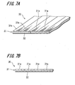
FIG. 7A is a perspective view illustrating one example of a magnetic path plate, and
FIG. 7B is a sectional view thereof according to an embodiment of the invention. -
FIG. 8A is a sectional view illustrating magnetic field lines of the sensor coil passing through the magnetic path plate, andFIG. 8B is a sectional view illustrating magnetic field lines of noise passing through the magnetic path plate according to an embodiment of the invention.
Fig. 8C is a more detailed view of the electromagnetic field emitted by the position indicator ofFig. 8A . -
FIG. 9 is a characteristic diagram illustrating curves indicating levels of receiving signals according to an embodiment of the invention. -
FIG. 10 is a perspective view illustrating one example of a personal computer utilizing the position detector according to an embodiment of the invention. -
FIG. 11 is an exploded perspective view illustrating a major part of a display according to an embodiment of the invention. -
FIG. 12A is a perspective view illustrating an overall position detector utilizing PDA, andFIG. 12B is an exploded perspective view illustrating the major part thereof according to an embodiment of the invention. -
FIG. 13 illustrates another example according to an embodiment of the invention. - Embodiments of the invention will now be described with reference to accompanied drawings
FIGS. 6 to 13 .
FIG. 6 is an exploded perspective view illustrating aposition detector 20 according to an embodiment of the invention. As shown in the figure, asensor substrate 27 and a magnetic path meansplate 30 are arranged between anupper case 26 and alower case 28. In the embodiment considered here the magnetic path means has a plate-like form and is referred to asmagnetic path plate 30 in the following. It is to be noted that the magnetic path means can have another form such as a curved, convex or concave shape. - The
upper case 26 includes adrawing plane 26a used for the position indicator 10 (not shown inFIG. 6 ). Themagnetic path plate 30 is arranged on a surface (lower case 28 side) opposite to a surface (upper case 26 side) where thesensor substrate 27 faces theposition indicator 10. Thesensor substrate 27 has asensor coil 21 that detects a coordinate indicated by theposition indicator 10. - The
sensor coil 21 includes asensor coil 21 x for detecting x coordinates provided on one surface thesensor substrate 27, and asensor coil 21 y (not shown inFIG. 6 ) for detecting y coordinates provided on the other surface thereof. Thesensor coil 21 includes asensor coil 21 x for detecting x coordinates provided on one surface thesensor substrate 27, and asensor coil 21 y (not shown inFIG. 6 ) for detecting y coordinates provided on the other surface thereof. It is preferable that the area in which thesensor coil 21 is arranged have an equal size as an area of the drawingplane 26a in thesensor substrate 27. - The
magnetic path plate 30 is utilized, when thesensor coil 21 receives an electromagnetic wave output from theposition indicator 10, for preventing thesensor coil 21 from receiving electromagnetic noise generated from an opposite side of theposition indicator 10. Further, in a case where a metallic plate or the like is placed on a side of thesensor coil 21 opposite to a side where theposition indicator 10 will eventually be located; that is, in a case where the position detector is placed on the metallic plate, the magnetic field generated by themagnetic path plate 30 over thesensor coil 21 can be prevented from attenuating in the metallic plate. Accordingly, themagnetic path plate 30 can effectively function if themagnetic path plate 30 has an area equal to or larger than an area in which thesensor coil 21 is arranged. It is desirable that themagnetic path plate 30 have further large area if the electromagnetic noise obliquely enters to the substrate on which thesensor coil 21 is arranged. - Next, the
magnetic path plate 30 utilized for the embodiment will be described in details.FIG. 7A is a partial perspective view illustrating a configuration example of themagnetic path plate 30, andFIG. 7B is a sectional view thereof according to an embodiment of the invention. Themagnetic path plate 30 includes anamorphous layer 31 andnon-amorphous layer 32 formed of metal with relative magnetic permeability lower than that ofamorphous layer 31. An example of metal used as thenon-amorphous layer 32 includes aluminum. Theamorphous layer 31 is formed by arranging a plurality of amorphous metal strips 31 a in parallel with the longitudinal axis thereof to form a plane. - The
amorphous layer 31 is extremely thin (approximately 20 µm), so that electric shielding obtained may not be effective. Themagnetic path plate 30 includes aluminum as metal having relative permeability lower than that of theamorphous layer 31. Since aluminum is light, the position detector made of aluminum can be made lighter as compared with the related art position detector made of a silicon steel plate. Further, cost can be reduced by using aluminum in manufacturing. Note that a material for formingnon-amorphous layer 32 is not limited to aluminum; however, any kinds of metal capable of providing electric shielding or those having relative permeability lower than that of theamorphous metal 31 a can be employed. -
FIGS. 8A, 8B are each a sectional view illustrating how the aforementionedmagnetic path plate 30 generates paths of magnetic flux. When theposition indicator 10 is located above the drawing region 26-a it may emit anelectromagnetic wave 50 that propagates into afirst direction 51 towards the drawing region 26-a. Thesenor coil 21 is arranged below the drawing region 26-a in order to receive theelectromagnetic wave 50 from thefirst direction 51. Hence, themagnetic path plate 30 is arranged behind thesensor coil 21 in thefirst direction 51.Fig. 8C shows a more detailed view of theelectromagnetic wave 50. -
FIG. 8A illustrates how themagnetic flux 33 generated by current from thesensor coil 21 passes through theamorphous layer 31 of themagnetic path plate 30. As shown in the figure, themagnetic flux 33 enters theamorphous metal 31 a, proceeds along theamorphous layer 31, and comes out of the surface of theamorphous metal 31 a of themagnetic path plate 30. In other words, theamorphous layer 31 generates the magnetic paths through which the magnetic flux passes. The dotted line in the figure shows amagnetic force line 33b in a case where noamorphous layer 31 is provided. In comparing the magnetic path plate having the amorphous layer 31 (solid line) with that without the amorphous layer 31 (dotted line), the magnetic force lines pass through theamorphous layer 31 and come out of the surface of theamorphous layer 31 in a case where themagnetic path plate 30 has theamorphous layer 31. This implies that theamorphous layer 31 generates the magnetic paths. - Likewise,
FIG. 8B illustrates howmagnetic flux 34 enters theamorphous metal 31 a from the opposite side of thesensor coil 21 provided above themagnetic path plate 30. Themagnetic flux 34 is so-called "magnetic noise". As shown in the figure, themagnetic flux 34 that will be noise enters fromnon-amorphous layer 32 into theamorphous layer 31 a, and comes out again of the surface of thenon-amorphous layer 31. Thus, themagnetic flux 34 or noise will not reach thesensor coil 21 due to the magnetic paths generated by theamorphous layer 31. Since theamorphous layer 31 generates the paths for themagnetic flux amorphous layer 31, and hence, external magnetic noise will not interfere with the magnetic field generated by thesensor coil 21. - It is to be noted that the arrangement of the
amorphous layer 31 on top of thenon-amorphous layer 32 as shown inFig. 8 is not essential. It is also possible to arrange thenon-amorphous layer 32 on top of theamorphous layer 31 as this provides substantially the same effect. - The invention is particularly beneficial for battery-powered hand-held electronic appliances, such as a personal digital assistant, a mobile communication device, such as a mobile phone or a smart phone, a navigation device, a digital camera or the like. As the signal-to-noise ratio improves less power is required for the reception which helps to extend the battery lifetime.
- Hereafter, an example that compares a position detector having the
magnetic path plate 30 of the embodiment with a position detector having the related art shielding plate will be described based on a graph inFIG. 9. FIG. 9 shows the graph representing the induced electromotive force generated from theposition indicator 10 that is measured in a region close to thepen point 14. The coordinate of thepen point 14 corresponds to the peak of the graph. The induced electromotive force is measured under the following three conditions: the detector having the related art electrostatic shielding, the detector without the related art electrostatic shielding, and the detector having the shielding plate of this embodiment. A horizontal axis of the graph represents coordinates; however, the scale is arbitrarily set. - A symbol "◆" of the graph shows an outcome measured with the detector without the magnetic path plate indicating no effect of noise. A symbol "x" of the graph shows an outcome measured with the detector having the magnetic path plate of the embodiment. A symbol "*" of the graph shows an outcome measured with the detector having the related art silicon steel plate, and a solid line of the graph shows an outcome measured with the detector having shielding used by those having ordinary skills in the art. The outcome shows that the detector without the magnetic path plate shows the highest signal level received by the sensor coil. Further, the detector having shielding of the ordinary metallic plate shows almost no signal level.
- As shown in
FIG. 9 , in comparing the detector having a combination of an amorphous layer and aluminum foil with the detector having a silicon steel plate, the detector having the amorphous layer and the aluminum foil shows a signal level approximately twice the detector having the silicon steel plate, thereby clearly showing an increase of the signal level. Since the aluminum foil is produced by expanding aluminum thinly and thus the obtained product is the aluminum layer. The graph shows that the detector having the amorphous layer and aluminum foil can acquire a higher signal level than the detector having the silicon steel plate. -
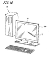
FIG. 10 is a configuration example of a computer apparatus employing a position detector according to an embodiment of the invention. In the configuration example, adisplay 200 connected to apersonal computer 100 includes a sensor 20 (not shown inFIG. 9 ), and aposition indicator 10 that is operated on the screen of thedisplay 200 to indicate a coordinate. -
FIG. 11 is an exploded perspective view illustrating main portions of thedisplay 200 shown inFIG. 10 . As shown in the figure, thesensor substrate 27 is placed on the opposite side of the position where theposition indicator 10 is placed on the surface of adisplay panel 201, and themagnetic path plate 30 is placed beneath thesensor substrate 27. A drivingcircuit board 202 driving thedisplay panel 201 is placed on the opposite side of thesensor substrate 27 located above themagnetic path plate 30. Adisplay panel 201 herein implies a liquid crystal panel. The liquid crystal panel includes a glass substrate, a backlight, a polarizing plate or the like; however, the liquid crystal panel according to this embodiment includes all these components. - The
display panel 201 having such configuration can cut off the noise generated by the drivingcircuit board 202 using themagnetic path plate 30. Thus, the user can operate theposition indicator 10 so as to draw directly on the surface of thedisplay 200 when inputting coordinates in thepersonal computer 100.FIGS. 10 and11 illustrate examples of thepersonal computer 100 where a main body and thedisplay 200 are separately configured; however, the main body and the display can be integrated such as a note-type computer. - As described so far, since the
magnetic path plate 30 is formed by stacking theamorphous layer 31 andaluminum layer 32, the electromagnetic noise generated by the drivingcircuit board 202 can be cut off, attenuation of the magnetic field due to eddy current can be prevented, and further, the detector can be reduced in weight. -
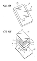
FIG. 12A is an overall view illustrating one example of a personal digital assistant (PDA) 40 as a mobile electronic apparatus, whereasFIG. 12B is an exploded perspective view illustrating main components thereof.FIG. 12B shows that a position detector ofPDA 40 includes thedisplay panel 201 having thesensor substrate 27, themagnetic path plate 30, and a display panel drivingcircuit board 41 located therebeneath. Thedisplay panel 201 herein implies a liquid crystal panel. - The position detector of the embodiment includes the
sensor coil 21 located between theposition indicator 10 and themagnetic path plate 30, and hence noise generated by the display panel drivingcircuit board 41 can be cut off. Further, attenuation of the magnetic field due to eddy current of apen coil 11, not shown inFIG. 13 , can be lowered. - Since the position detector of the embodiment includes the
magnetic path plate 30 having theamorphous layer 31 andnon-amorphous layer 32, for which aluminum is used, the position detector of the embodiment can effectively be reduced in weight in comparison with the position detector having the related art silicon steel plate for electromagnetic shielding. Thus, the position detector of the embodiment can be used, in combination with the position indicator, for an electronic organizer, a portable video game player, and a mobile phone as well as the PDA. - Further,
FIGS. 10 to 12A ,12B show the embodiments of thedisplay panel 201 having the liquid crystal panel; however, the embodiments are not limited thereto, and a display panel having an electroluminescence device or light emitting diode may also be employed. In addition, the display panel may be used for a display device known as an electronic paper, or plasma display. -
FIG. 13 illustrates an example of the position detector having thesensor substrate 27 located above thedisplay panel 201. Thesensor substrate 27 includes a transparent substrate such as glass, while thesensor coil 21 is formed with fine lines generally invisible with the naked eye, and is formed of a transparent conducting material such as indium tin oxide (ITO). Since light passes through thesensor substrate 27 and thesensor coil 21 is invisible with the naked eye, thesensor substrate 27 can be arranged on the surface of the display panel 201 (i.e., display surface).
In this configuration, themagnetic path plate 30 is arranged on the opposite side of thesensor substrate 27 located beneath thedisplay panel 201. In other words, the magnetic path plate is placed on the opposite side of thesensor substrate 27 on thedisplay panel 201. Further, a material or thesensor coil 21 may include metallic fine lines in addition to the transparent conductive material. - It should be understood by those skilled in the art that various modifications, combinations, sub-combinations and alterations may occur depending on design requirements and other factors insofar as they are within the scope of the appended claims or the equivalents thereof.
Claims (13)
- A position detector (20) comprising:sensor means (27) having a sensor coil (21) for receiving an electromagnetic wave output (50) from a position indicator (10); andmagnetic path means (30) extending over an area equal to or larger than an area in which the sensor coil is arranged, the magnetic path means comprising a first layer (31, 31 a) formed of amorphous metal and a second layer (32) formed of non-amorphous metal, the second layer having a relative magnetic permeability lower than that of the first layer.
- A position detector according to claim 1, wherein the amorphous layer includes aluminum.
- The position detector of claim 1 or 2, the magnetic path means being a magnetic path plate.
- The position detector of claim 1, 2 or 3, the first and second layers of the magnetic path means being stacked.
- The position detector of any one of the preceding claims, the sensor means being arranged for receiving the electromagnetic wave output from a first direction (51), the magnetic path means being arranged behind the sensor means in the first direction.
- The position detector of any one of the preceding claims, the sensor means having a substrate carrying the sensor coil.
- The position detector of any one of the preceding claims, the first layer being formed a plurality of amorphous metal strips (31 a) being arranged in parallel.
- The position detector of any one of the preceding claims, the first layer having a thickness below 50 µm, preferably approximately 20 µm.
- A display device comprising:a position detector (20) in accordance with any one of the preceding claims ; anda display unit (201) provided on one surface of the sensor means.
- The display device of claim 9, the sensor means having a substrate carrying the sensor coil, the display unit being arranged on one surface of the substrate.
- The display device according to claim 10, wherein the substrate is formed of a transparent material, and the display unit is placed between the sensor substrate and the magnetic path means.
- A battery-powered hand-held electronic appliance having a display device in accordance with claims 9, 10 or 11.
- The electronic appliance of claim 12, being a personal digital assistant, a mobile communication device, such as a mobile phone or a smart phone, a navigation device or a digital camera.
Applications Claiming Priority (1)
| Application Number | Priority Date | Filing Date | Title |
|---|---|---|---|
| JP2007165469A JP4972782B2 (en) | 2007-06-22 | 2007-06-22 | Position detection device |
Publications (3)
| Publication Number | Publication Date |
|---|---|
| EP2015030A2 true EP2015030A2 (en) | 2009-01-14 |
| EP2015030A3 EP2015030A3 (en) | 2012-01-11 |
| EP2015030B1 EP2015030B1 (en) | 2013-06-05 |
Family
ID=39766839
Family Applications (1)
| Application Number | Title | Priority Date | Filing Date |
|---|---|---|---|
| EP08158553.1A Expired - Fee Related EP2015030B1 (en) | 2007-06-22 | 2008-06-19 | Position detector and display device |
Country Status (5)
| Country | Link |
|---|---|
| US (1) | US8149220B2 (en) |
| EP (1) | EP2015030B1 (en) |
| JP (1) | JP4972782B2 (en) |
| CN (1) | CN101329607B (en) |
| TW (1) | TWI429882B (en) |
Cited By (2)
| Publication number | Priority date | Publication date | Assignee | Title |
|---|---|---|---|---|
| DE102012224386B3 (en) * | 2012-12-27 | 2014-02-13 | Sick Ag | Inductive sensor |
| EP2546732A3 (en) * | 2011-07-11 | 2015-12-09 | Samsung Electronics Co., Ltd. | Input device |
Families Citing this family (34)
| Publication number | Priority date | Publication date | Assignee | Title |
|---|---|---|---|---|
| JP5094376B2 (en) * | 2007-12-28 | 2012-12-12 | 株式会社ワコム | Position detection device |
| KR100975868B1 (en) * | 2008-07-23 | 2010-08-13 | 삼성모바일디스플레이주식회사 | Flat panel display device |
| WO2010138385A1 (en) * | 2009-05-27 | 2010-12-02 | Analog Devices, Inc. | Multiuse optical sensor |
| JP5270482B2 (en) * | 2009-07-13 | 2013-08-21 | 株式会社ワコム | Position detecting device and sensor unit |
| JP5430339B2 (en) | 2009-10-19 | 2014-02-26 | 株式会社ワコム | Position detecting device and position indicator |
| TWI424386B (en) * | 2010-03-19 | 2014-01-21 | Prime View Int Co Ltd | Bi-stable display |
| CN102298226B (en) * | 2010-06-22 | 2014-05-14 | 元太科技工业股份有限公司 | Bistable-state display |
| US8344836B2 (en) | 2010-09-17 | 2013-01-01 | Apple Inc. | Protective cover for a tablet computer |
| US8395465B2 (en) * | 2010-09-17 | 2013-03-12 | Apple Inc. | Cover for an electric device |
| JP5459795B2 (en) * | 2011-06-06 | 2014-04-02 | 株式会社ワコム | Electronics |
| KR101804579B1 (en) | 2011-07-11 | 2017-12-05 | 삼성전자주식회사 | Inputting device |
| WO2013068795A1 (en) * | 2011-11-11 | 2013-05-16 | Nokia Corporation | An apparatus and a method for metal detection involving a mobile terminal with a display |
| JP5831902B2 (en) | 2011-12-27 | 2015-12-09 | 株式会社ワコム | Operation switch device |
| JP6268651B2 (en) * | 2012-02-03 | 2018-01-31 | アモセンス カンパニー,リミテッド | Magnetic field shielding sheet for digitizer, method of manufacturing the same, and portable terminal device using the same |
| JP5892595B2 (en) * | 2012-02-06 | 2016-03-23 | 株式会社ワコム | Position indicator |
| JP5137150B1 (en) | 2012-02-23 | 2013-02-06 | 株式会社ワコム | Handwritten information input device and portable electronic device provided with handwritten information input device |
| US9502922B2 (en) | 2012-02-29 | 2016-11-22 | Panasonic Intellectual Property Management Co., Ltd. | Charging apparatus |
| JP6455709B2 (en) * | 2012-03-14 | 2019-01-23 | オレンジ ミュージック エレクトロニック カンパニー リミテッド | Audiovisual guidance device |
| CN104412728B (en) * | 2012-06-04 | 2017-12-05 | 阿莫先恩电子电器有限公司 | Digital quantizer is with magnetic field shielding piece and preparation method thereof and utilizes its portable terminal |
| KR101999119B1 (en) * | 2012-07-11 | 2019-07-12 | 삼성전자 주식회사 | Method using pen input device and terminal thereof |
| WO2014054499A1 (en) * | 2012-10-04 | 2014-04-10 | 株式会社東芝 | Magnetic sheet and display using same |
| USD748630S1 (en) * | 2012-10-09 | 2016-02-02 | Logitech Europe S.A. | Wireless touch sensor device |
| TW201445410A (en) * | 2013-05-22 | 2014-12-01 | Waltop Int Corp | Electromagnetic induction panel structure and method of manufacturing the same, and electromagnetic handwriting input device |
| JP2015026235A (en) | 2013-07-26 | 2015-02-05 | 株式会社ワコム | Electromagnetic induction sensor, coverlay member for electromagnetic induction sensor, and method of manufacturing electromagnetic induction sensor |
| KR101800295B1 (en) * | 2013-09-04 | 2017-12-20 | 엘지디스플레이 주식회사 | Position detection method, position detection apparatus, antenna apparatus, and display apparatus |
| KR102193915B1 (en) * | 2014-02-10 | 2020-12-23 | 삼성디스플레이 주식회사 | Touch sensor substrate and display apparatus having the touch sensor substrate |
| CN103941952B (en) | 2014-03-31 | 2017-03-29 | 上海天马微电子有限公司 | A kind of induction touch base plate and inductive touch control display device |
| CN111665957B (en) * | 2014-07-08 | 2024-04-23 | 株式会社和冠 | Position indicator |
| WO2016186191A1 (en) | 2015-05-21 | 2016-11-24 | 株式会社ワコム | Active stylus |
| JP6618536B2 (en) | 2015-07-29 | 2019-12-11 | 株式会社ワコム | Coordinate input device |
| EP3367217B1 (en) * | 2015-10-22 | 2022-04-20 | Wacom Co., Ltd. | Position indicator and position detection apparatus |
| JP6698386B2 (en) | 2016-03-10 | 2020-05-27 | 株式会社ジャパンディスプレイ | Display device and touch detection device |
| CN113994307A (en) | 2019-06-20 | 2022-01-28 | 株式会社和冠 | Position detecting device |
| US20240094844A1 (en) * | 2021-03-01 | 2024-03-21 | Sharp Kabushiki Kaisha | Display device |
Citations (4)
| Publication number | Priority date | Publication date | Assignee | Title |
|---|---|---|---|---|
| EP0159498A1 (en) | 1984-03-06 | 1985-10-30 | Wacom Co., Ltd. | Coordinate input device with display |
| US4704501A (en) | 1984-12-28 | 1987-11-03 | Wacom Co., Ltd. | Position detecting device |
| US4956526A (en) | 1989-07-18 | 1990-09-11 | Kabushikikaisha Wacom | Digitizer having flat tablet with magnetic shield plate |
| US20060267580A1 (en) | 2005-04-26 | 2006-11-30 | Masamitsu Fukushima | Position detection device and position input device |
Family Cites Families (10)
| Publication number | Priority date | Publication date | Assignee | Title |
|---|---|---|---|---|
| JPS6092333U (en) * | 1983-11-24 | 1985-06-24 | シャープ株式会社 | handwriting input device |
| US5130500A (en) * | 1989-07-18 | 1992-07-14 | Kabushikikaisha Wacom | Digitizer having flat tablet with magnetic shield plate |
| JPH06309085A (en) * | 1993-04-20 | 1994-11-04 | Seiko Instr Inc | Coordinate reader |
| JP2591585B2 (en) | 1993-10-18 | 1997-03-19 | 平岡織染株式会社 | Electromagnetic wave shielding laminated sheet |
| JPH1049287A (en) * | 1996-07-29 | 1998-02-20 | Wacom Co Ltd | Tablet of position detecting device |
| KR20010094773A (en) * | 2001-03-16 | 2001-11-03 | 장광식 정윤철 | Touch Panel with polarizer and Flat Panel Display with Touch Panel and manufacturing method thereof |
| CN1247961C (en) | 2001-06-29 | 2006-03-29 | 松下电工株式会社 | Position sensor |
| CN2567694Y (en) * | 2002-09-16 | 2003-08-20 | 台均实业有限公司 | Touch control display screen with conductor lattice electromagnetic induction layer in it |
| JP2006065757A (en) * | 2004-08-30 | 2006-03-09 | Wacom Co Ltd | Coordinate indicator |
| JP4568661B2 (en) * | 2005-08-30 | 2010-10-27 | 株式会社ワコム | Position detection device, position input device, and computer |
-
2007
- 2007-06-22 JP JP2007165469A patent/JP4972782B2/en active Active
-
2008
- 2008-06-19 EP EP08158553.1A patent/EP2015030B1/en not_active Expired - Fee Related
- 2008-06-19 US US12/142,717 patent/US8149220B2/en active Active
- 2008-06-20 TW TW097123088A patent/TWI429882B/en not_active IP Right Cessation
- 2008-06-23 CN CN2008101286918A patent/CN101329607B/en not_active Expired - Fee Related
Patent Citations (4)
| Publication number | Priority date | Publication date | Assignee | Title |
|---|---|---|---|---|
| EP0159498A1 (en) | 1984-03-06 | 1985-10-30 | Wacom Co., Ltd. | Coordinate input device with display |
| US4704501A (en) | 1984-12-28 | 1987-11-03 | Wacom Co., Ltd. | Position detecting device |
| US4956526A (en) | 1989-07-18 | 1990-09-11 | Kabushikikaisha Wacom | Digitizer having flat tablet with magnetic shield plate |
| US20060267580A1 (en) | 2005-04-26 | 2006-11-30 | Masamitsu Fukushima | Position detection device and position input device |
Cited By (4)
| Publication number | Priority date | Publication date | Assignee | Title |
|---|---|---|---|---|
| EP2546732A3 (en) * | 2011-07-11 | 2015-12-09 | Samsung Electronics Co., Ltd. | Input device |
| US9626038B2 (en) | 2011-07-11 | 2017-04-18 | Samsung Electronics Co., Ltd | Input device |
| DE102012224386B3 (en) * | 2012-12-27 | 2014-02-13 | Sick Ag | Inductive sensor |
| EP2749850A1 (en) | 2012-12-27 | 2014-07-02 | Sick Ag | Inductive sensor |
Also Published As
| Publication number | Publication date |
|---|---|
| TW200921054A (en) | 2009-05-16 |
| EP2015030A3 (en) | 2012-01-11 |
| US8149220B2 (en) | 2012-04-03 |
| JP2009003796A (en) | 2009-01-08 |
| CN101329607A (en) | 2008-12-24 |
| CN101329607B (en) | 2012-10-31 |
| EP2015030B1 (en) | 2013-06-05 |
| TWI429882B (en) | 2014-03-11 |
| US20090160790A1 (en) | 2009-06-25 |
| JP4972782B2 (en) | 2012-07-11 |
Similar Documents
| Publication | Publication Date | Title |
|---|---|---|
| EP2015030B1 (en) | Position detector and display device | |
| EP2703961B1 (en) | Touch screen device | |
| KR102125404B1 (en) | Touch sensing system and diplay device | |
| JP5153890B2 (en) | Touch panel and electronic device equipped with touch panel | |
| JP2014160473A (en) | Portable electronic equipment | |
| US8547343B2 (en) | Display apparatus | |
| CN110286805A (en) | Electronic equipment and its control method | |
| CN101498849A (en) | Hand-written LCD | |
| US20230236668A1 (en) | Capacitance Module with an Antenna and Haptics | |
| KR20160121868A (en) | digitizer and portable apparatus having the same | |
| KR102111782B1 (en) | Coordinates ditecting apparatus having electromagnetic resonance touch sensor and ir touch sensor | |
| KR20140067488A (en) | Touchscreen pannel and writing presure sensing method the same | |
| CN110308770A (en) | Electronic equipment and its control method | |
| KR101935024B1 (en) | Electrostatic Capacity Type Electronic Board | |
| KR101935025B1 (en) | Manufacturing Method for Electrostatic Capacity Type Electronic Board | |
| KR101935023B1 (en) | Electrostatic Capacity Type Electronic Board | |
| US20240012524A1 (en) | Antenna in a Capacitance Module | |
| CN212112431U (en) | Touch panel and notebook computer | |
| US11687188B2 (en) | Input device with near-field communication | |
| CN110312030B (en) | Electronic device and control method thereof | |
| KR101581412B1 (en) | Digitizer | |
| CN110300206A (en) | Housing unit, electronic equipment and its control method | |
| KR20150113669A (en) | Coordinates input apparatus | |
| JP6015952B2 (en) | Electronics | |
| KR20210064439A (en) | Touch apparatus |
Legal Events
| Date | Code | Title | Description |
|---|---|---|---|
| PUAI | Public reference made under article 153(3) epc to a published international application that has entered the european phase |
Free format text: ORIGINAL CODE: 0009012 |
|
| PUAI | Public reference made under article 153(3) epc to a published international application that has entered the european phase |
Free format text: ORIGINAL CODE: 0009012 |
|
| AK | Designated contracting states |
Kind code of ref document: A2 Designated state(s): AT BE BG CH CY CZ DE DK EE ES FI FR GB GR HR HU IE IS IT LI LT LU LV MC MT NL NO PL PT RO SE SI SK TR |
|
| AX | Request for extension of the european patent |
Extension state: AL BA MK RS |
|
| PUAL | Search report despatched |
Free format text: ORIGINAL CODE: 0009013 |
|
| AK | Designated contracting states |
Kind code of ref document: A3 Designated state(s): AT BE BG CH CY CZ DE DK EE ES FI FR GB GR HR HU IE IS IT LI LT LU LV MC MT NL NO PL PT RO SE SI SK TR |
|
| AX | Request for extension of the european patent |
Extension state: AL BA MK RS |
|
| RIC1 | Information provided on ipc code assigned before grant |
Ipc: G06F 3/046 20060101ALI20111208BHEP Ipc: G06F 3/033 20060101ALI20111208BHEP Ipc: G01D 5/20 20060101AFI20111208BHEP |
|
| 17P | Request for examination filed |
Effective date: 20120711 |
|
| 17Q | First examination report despatched |
Effective date: 20120803 |
|
| AKX | Designation fees paid |
Designated state(s): DE GB |
|
| GRAP | Despatch of communication of intention to grant a patent |
Free format text: ORIGINAL CODE: EPIDOSNIGR1 |
|
| RIC1 | Information provided on ipc code assigned before grant |
Ipc: G06F 3/0354 20130101ALI20121219BHEP Ipc: G01D 5/20 20060101AFI20121219BHEP Ipc: G06F 3/046 20060101ALI20121219BHEP |
|
| GRAS | Grant fee paid |
Free format text: ORIGINAL CODE: EPIDOSNIGR3 |
|
| GRAA | (expected) grant |
Free format text: ORIGINAL CODE: 0009210 |
|
| AK | Designated contracting states |
Kind code of ref document: B1 Designated state(s): DE GB |
|
| REG | Reference to a national code |
Ref country code: GB Ref legal event code: FG4D |
|
| REG | Reference to a national code |
Ref country code: DE Ref legal event code: R096 Ref document number: 602008025118 Country of ref document: DE Effective date: 20130801 |
|
| PLBE | No opposition filed within time limit |
Free format text: ORIGINAL CODE: 0009261 |
|
| STAA | Information on the status of an ep patent application or granted ep patent |
Free format text: STATUS: NO OPPOSITION FILED WITHIN TIME LIMIT |
|
| 26N | No opposition filed |
Effective date: 20140306 |
|
| REG | Reference to a national code |
Ref country code: DE Ref legal event code: R097 Ref document number: 602008025118 Country of ref document: DE Effective date: 20140306 |
|
| PGFP | Annual fee paid to national office [announced via postgrant information from national office to epo] |
Ref country code: DE Payment date: 20210618 Year of fee payment: 14 |
|
| PGFP | Annual fee paid to national office [announced via postgrant information from national office to epo] |
Ref country code: GB Payment date: 20210625 Year of fee payment: 14 |
|
| REG | Reference to a national code |
Ref country code: DE Ref legal event code: R119 Ref document number: 602008025118 Country of ref document: DE |
|
| GBPC | Gb: european patent ceased through non-payment of renewal fee |
Effective date: 20220619 |
|
| PG25 | Lapsed in a contracting state [announced via postgrant information from national office to epo] |
Ref country code: GB Free format text: LAPSE BECAUSE OF NON-PAYMENT OF DUE FEES Effective date: 20220619 Ref country code: DE Free format text: LAPSE BECAUSE OF NON-PAYMENT OF DUE FEES Effective date: 20230103 |