EP2016659B1 - Power supply system - Google Patents
Power supply system Download PDFInfo
- Publication number
- EP2016659B1 EP2016659B1 EP20070811849 EP07811849A EP2016659B1 EP 2016659 B1 EP2016659 B1 EP 2016659B1 EP 20070811849 EP20070811849 EP 20070811849 EP 07811849 A EP07811849 A EP 07811849A EP 2016659 B1 EP2016659 B1 EP 2016659B1
- Authority
- EP
- European Patent Office
- Prior art keywords
- connector
- output
- voltage
- indicator
- power
- Prior art date
- Legal status (The legal status is an assumption and is not a legal conclusion. Google has not performed a legal analysis and makes no representation as to the accuracy of the status listed.)
- Not-in-force
Links
Images


Classifications
-
- H—ELECTRICITY
- H04—ELECTRIC COMMUNICATION TECHNIQUE
- H04B—TRANSMISSION
- H04B1/00—Details of transmission systems, not covered by a single one of groups H04B3/00 - H04B13/00; Details of transmission systems not characterised by the medium used for transmission
- H04B1/06—Receivers
- H04B1/16—Circuits
- H04B1/1607—Supply circuits
-
- H—ELECTRICITY
- H01—ELECTRIC ELEMENTS
- H01R—ELECTRICALLY-CONDUCTIVE CONNECTIONS; STRUCTURAL ASSOCIATIONS OF A PLURALITY OF MUTUALLY-INSULATED ELECTRICAL CONNECTING ELEMENTS; COUPLING DEVICES; CURRENT COLLECTORS
- H01R13/00—Details of coupling devices of the kinds covered by groups H01R12/70 or H01R24/00 - H01R33/00
- H01R13/46—Bases; Cases
- H01R13/465—Identification means, e.g. labels, tags, markings
-
- H—ELECTRICITY
- H01—ELECTRIC ELEMENTS
- H01R—ELECTRICALLY-CONDUCTIVE CONNECTIONS; STRUCTURAL ASSOCIATIONS OF A PLURALITY OF MUTUALLY-INSULATED ELECTRICAL CONNECTING ELEMENTS; COUPLING DEVICES; CURRENT COLLECTORS
- H01R27/00—Coupling parts adapted for co-operation with two or more dissimilar counterparts
-
- H—ELECTRICITY
- H01—ELECTRIC ELEMENTS
- H01R—ELECTRICALLY-CONDUCTIVE CONNECTIONS; STRUCTURAL ASSOCIATIONS OF A PLURALITY OF MUTUALLY-INSULATED ELECTRICAL CONNECTING ELEMENTS; COUPLING DEVICES; CURRENT COLLECTORS
- H01R29/00—Coupling parts for selective co-operation with a counterpart in different ways to establish different circuits, e.g. for voltage selection, for series-parallel selection, programmable connectors
-
- H—ELECTRICITY
- H01—ELECTRIC ELEMENTS
- H01R—ELECTRICALLY-CONDUCTIVE CONNECTIONS; STRUCTURAL ASSOCIATIONS OF A PLURALITY OF MUTUALLY-INSULATED ELECTRICAL CONNECTING ELEMENTS; COUPLING DEVICES; CURRENT COLLECTORS
- H01R31/00—Coupling parts supported only by co-operation with counterpart
- H01R31/06—Intermediate parts for linking two coupling parts, e.g. adapter
-
- H—ELECTRICITY
- H02—GENERATION; CONVERSION OR DISTRIBUTION OF ELECTRIC POWER
- H02J—CIRCUIT ARRANGEMENTS OR SYSTEMS FOR SUPPLYING OR DISTRIBUTING ELECTRIC POWER; SYSTEMS FOR STORING ELECTRIC ENERGY
- H02J1/00—Circuit arrangements for dc mains or dc distribution networks
- H02J1/08—Three-wire systems; Systems having more than three wires
- H02J1/082—Plural DC voltage, e.g. DC supply voltage with at least two different DC voltage levels
Definitions
- Such electronic devices include cellular phones, portable computers, MP3 players, personal digital assistants (PDAs), etc.
- PDAs personal digital assistants
- a person may own one or all of such portable electronic devices and each portable electronic device may have a separate power supply system associated with it.
- the use of many different power supplies is not desirable, since power supplies (sometimes called "power bricks") are often very bulky and cumbersome. For example, if a person owns a portable computer, a cellular phone, and an MP3 player, that person would also own three portable power supplies for those three portable electronic devices. If that person is traveling, it is quite cumbersome for that person to carry all of those portable power supplies with him.
- U.S. Patent No. 5,838,554 describes the use of a single power adapter for use with a plurality of different tips which can connect to different types of portable electronic devices. Each tip includes a different electrical component in it. In use, a tip is connected to the power adapter. The circuitry in the power adapter senses the electrical component in the tip and a feedback signal is provided to power circuitry containing a programmed IC chip. The power circuitry, in turn, provides a first output voltage. If a second tip with a different electrical component is selected, a different feedback signal is sent to the power circuitry and the power circuitry then produces a second output voltage associated with the second tip.
- US 2005/021982 A1 discloses a power converter with output voltage level indicating device.
- the power converter is adapted to provide more than two output voltages and these voltages are supplied independent from a state of a switch.
- US 2005/259456 A1 discloses a power supply device having a number of voltages being permanently supplied at an output connector terminal with a total of five electrical contacts.
- US 2002 0043942 discloses a multiple output power adapter, wherein a first or a second output voltage can be supplied by an output connector.
- Embodiments of the invention address these and other problems, collectively and individually.
- Embodiments of the invention are directed to power supply systems and methods for using power supply systems according to the appended claims.
- Embodiments of the invention are directed to power supply systems.
- An exemplary power supply system comprises a power adapter which may house a power circuit.
- the power circuit may output a plurality of voltages (e.g., 16 VDC or 19.5 VDC).
- the voltages may be output simultaneously from the power circuit or may be output independently from the power circuit depending on the state of an external switch.
- Various connectable connectors such as connector tips can be mechanically and electrically coupled to an output connector in the power adapter.
- the various connectable connectors may be used with different electronic devices.
- Any suitable type of electronic device can be powered by the power supply systems according to embodiments of the invention.
- Examples of electronic devices comprise notebook computers, cell phones, MP3 players, televisions, etc.
- the output connector coupled to the power circuit, and the connectable connectors that are connectable to the output connector may have any suitable shape and/or configuration.
- Each connectable connector may be cooperatively structured with the output connector so that it can be easily connected to and separated from the output connector.
- the output connector may be a female type connector, and may mechanically mate with male-type first and second connectable connectors (or vice versa).
- Each connectable connector and each output connector can also have a plurality of electrical conductors with corresponding electrical contacts.
- connectable connectors may be in any suitable form.
- connectable connectors may be in the form of connector tips, connector wires, connection apparatuses, etc.
- a preferred connectable connector may be in the form of a connector tip, which would be in between the power adapter and the electronic device being powered.
- a power circuit in a power supply system outputs a plurality of voltages (e.g., two voltages - 16V and 19V), and the selection of a connector tip or the like can determine which voltage will be ultimately output.
- the power circuit in the power supply system may also output different voltages depending on the state of a power switch.
- the connector tips can be used to charge electronic devices such as notebook computers.
- a universal power supply can output at least two discrete voltages of about +16VDC (+/- 1 or 2 Volts) and about +19.5VDC (+/- 1 or 2 Volts) and can be used to provide power to most notebook computers on the market today.
- the power circuit in the power supply is adapted to provide only two discrete voltages to simplify the design of the power supply and power circuit.
- a notebook computer may be designed to work with a specific input voltage such as 20 V, it has been determined that the notebook computer may tolerate a slight deviation from 20V. The typical deviation could be +/- 1 or 2 Volts.
- a universal power supply could use a connector tip to output 19.5 VDC, it would be able to supply power to notebook computers that are designed to accept 19 V, 19.5 V, and 20V.
- one connector tip type may be provided to provide power to a number of brands of notebook computers, instead of one brand of notebook computers as long as the mechanical tip type can fit into the power ports of such notebook computers.
- Current universal power supplies may have as many as 37 connector tips that work with a single power brick. Having too many connector tips can be cumbersome as well as confusing. Having too many connector tips with too may different voltage ratings can also increase the chances that the consumer may use the incorrect one and damage his notebook computer. Too many connector tips with too many different voltages may also increase the overall cost of the universal power supply system.
- a first connector tip type may provide an output voltage at about 19.5 V when connected to the output connector and may have relative dimensions (OD/ID) of 4.75/1.7, 5.5/1.7, 5.5/2.1, 5.5/2.5, 6/1.4, 7.4/0.6 corresponding to 6 connector tips.
- a second connector tip type may output a voltage of 16V when connected to the output connector and may have relative dimensions (OD/ID) of 5.5/2.5, 6/1.4, 6.3/3 corresponding to 3 connector tips.
- a power adapter comprising a power circuit and an output connector, (ii) a first type of connector tip and multiple physical configurations of that first type of connector tip, and (ii) a second type of connector tip and multiple physical configurations of that second type of connector tip.
- the power adapter can include a low powered female USB port (at least one) on the body of the adapter or a combination of ports (e.g., a female USB port and a female FireWire port).
- the ports can be selected based on available/common charging cables for devices.
- the power supply system comprises a power circuit adapted to generate a first output voltage and a second output voltage at the same time, and an output connector coupled to the power circuit.
- the output connector includes a plurality of electrical contacts including a first set of contacts adapted to provide the first output voltage and a second set of electrical contacts adapted to provide the second - output voltage at the same time as the first output voltage.
- the first and second sets of contacts are different.
- a first connector e.g., a first connector tip
- a second connector e.g., a second connector tip
- a second connector tip can be configured to connect to the output connector and electrically couple to the second set of contacts to provide the second output voltage to a second electronic device (e.g., a portable computer made by manufacture B).
- a second electronic device e.g., a portable computer made by manufacture B
- the different output voltages that can be provided by the contacts in the output connector can range from about 15-17 VDC (or 14-17 VDC) for a first connector, and about 18-20 VDC (or 17-21 VDC) for a second connector.
- the connectable connector does not have an electrical component that provides feedback to a power circuit to cause the power circuit to generate a specific voltage. Rather, in this embodiment of the invention, the voltages are always available and the voltage output that is ultimately provided by the power supply system depends on the connectable connector that is connected to the output connector that is coupled to the power circuit.
- each connector tip can act as a jumper to different sets of contacts in the output connector to output the correct voltage.
- the output connector can have a plurality of electrical contacts including contacts A, B, and C.
- the first connector tip may have contacts that connect to a first set of contacts A and B in the output connector to produce a first output voltage associated with a first electronic device.
- a second connector tip may have contacts that connect to a second set of contacts A and C in the output connector to produce a second output voltage associated with a second electronic device.
- FIG. 1(a) shows a power supply system 100 according to an embodiment of the invention.
- the power supply system 100 includes a power adapter 10 including a casing (e.g., a plastic casing) 10(a) and an optional auxiliary connector port 10(b) in the casing.
- a wire 28 (or cable) couples an output connector 30 to the power adapter 10.
- the power adapter 10 may include power supply components and/or power circuit components including transformers, rectifiers, inverters, etc.
- Another wire 24 couples an input connector 20 to the power adapter 10.
- the input connector 20 may be a household plug that plugs into an AC power source.
- the input connector 20 may be a plug (e.g., a cigarette lighter plug) that plugs into a DC power source.
- the power supply system 100 may also include a first connector 32, which may be in the form of connector tip.
- the connector 32 may include a body portion 32(a) that is configured to mate with the output connector 30, and a mating portion 32(b) which mates with a port of a first electronic device (not shown).
- the first connector 32 may also have electrical contacts that electrically couple to only a certain set of electrical contacts (e.g., contacts A and B) in a plurality of contacts (e.g., contacts A, B, and C) in the output connector 30.
- the power supply system 100 may also include a second connector 33, which may be in the form of connector tip.
- the second connector 33 may include a body portion 33(a) that is configured to mate with the output connector 30 when the first connector 32 is not used.
- the second connector 33 may also include a mating portion 33(b) which mates with a port of a second electronic device (not shown).
- the second connector 33 may also have electrical contacts that electrically couple to only a certain set of electrical contacts (e.g., contacts A and C) in a plurality of contacts (e.g., contacts A, B, and C) in the output connector 30.
- the mating portions 32(b), 33(b) of the respective connectors 32, 33 may have different form factors as they are used with different port configurations on different electronic devices.
- the body portions 32(a), 33(a) of the respective connectors 32, 33 may have the same form factors as they are capable of connecting to the same output connector 30 (this is also applicable to later described embodiments).
- the body portions 32(a), 33(a) including different sets of contacts which will electrically couple to corresponding sets of contacts in the output connector 30.
- some members of the sets may be the same in some cases, but the sets are different.
- a first connector may have corresponding connectors A and B, while a second connector may have corresponding contacts A and C.
- the sets of contacts i.e., A-B, and A-C
- the sets of contacts are different, yet they have one common member A. In other embodiments, it is not necessary for the sets to have at least one common member.
- FIG. 1(b) shows an auxiliary connection device 50, which includes an auxiliary connector 52 including a body portion 52(a) and a mating portion 52(b).
- the mating portion 52(b) can be a plug which can plug into the auxiliary connector port 10(b) in the power adapter 10 shown in FIG. 1(a) .
- Another connector 54 including a body portion 54(a) and a connector portion 54(b) may be coupled to the auxiliary connector 52 via a wire 58.
- the auxiliary connection device 50 can provide low voltages to low voltages devices such as cell phones, while the connectors 32, 33 shown in FIG. 1(a) can provide higher voltages to higher voltage devices such as notebook computers.
- FIG. 2(a) shows a connector 60 in the form of a connector tip.
- the connector 60 includes a body portion 60(a) comprising plastic and a mating portion 60(b) comprising electrical contacts.
- FIG. 2(b) shows a first connector including electrical contacts 60(c), 60(d), which would connect to corresponding contacts in an output connector (not shown) to provide a first output voltage.
- FIG. 2(c) shows a second connector including electrical contacts 60(c) and 60(e), which would connect to corresponding contacts in an output connector (not shown) to provide a second output voltage.
- FIGS. 3(a) and 3(b) show end views of the connectors shown in FIGS. 2(b) and 2(c) .
- the cable can be completely detachable from an adapter body (e.g., the "brick") and the connector tip may be a permanent part of the cable.
- the connector between the cable and adapter body uses the method described above to output one of the available voltages from a single output connector.
- the adapter body can provide output voltage contacts that are covered by a slide, such that the user would have to move the slide to one side to expose either the 16 VDC or 19 VDC contact in the output connector. By selecting one contact, the other is rendered useless by the slide which covers the unselected contact.
- the power supply system described above can be used in any suitable manner.
- a user may first obtain the above-described power supply system. Then, the user may look on a chart or the like (an example of a chart is provided below), to match his first electronic device (e.g., a notebook computer) to a first connectable connector (e.g., a connector tip). The consumer may thereafter connect the first connectable connector to the output connector coupled to the above-described power circuit. The connected first connector will then output a specific voltage (e.g., 16 VDC), even though the power circuit in the power adapter and the output connector coupled to the power circuit are outputting a plurality of voltages. If the consumer has a second electronic device that operates at a different voltage than the first electronic device, then the user may detach the first connector from the output connector and may then attach the second connector to the output connector and the second electronic device to power the second electronic device.
- a specific voltage e.g. 16 VDC
- FIGS. 4-5 Exemplary power circuits that can be used with the embodiments described above with respect to FIGS. 1-3 are described in FIGS. 4-5 .
- FIG. 4 shows a block diagram of a power circuit according to an embodiment of the invention.
- the power circuit converts AC power, for example from a wall socket, to DC power that may be used to power a portable device. As shown, there is one AC input and there are two DC outputs.
- the power circuit includes an AC input line 78, which provides an AC voltage (e.g., 100-240 VAC) to a rectifier and an optional filter 80.
- the rectifier and filter 80 changes the AC input voltage to a DC output voltage (e.g., 50-120 VDC).
- the DC output voltage is then fed to an inverter 82, which generates an AC signal (e.g., 20 kHz at 50-120 VAC) that is stepped down in voltage by a transformer 84 (e.g., 20-60 VAC).
- the stepped-down AC voltage is then sent to another rectifier and optional filter combination 86, where the AC voltage is changed to a DC voltage (e.g., 25-60 VDC).
- the DC voltage is then fed to different regulators 88 and 90 which produce output voltages at contacts 92, 94 respectively.
- the regulators 88 and 90 generate voltages of 19.5 VDC and 16 VDC, though in other embodiments, other voltage may be provided.
- Feedback lines 96 and 98 provide signals back to the inverter 82 to regulate the output voltages.
- a first connector tip that is configured to deliver 19.5 VDC to an electronic device may have contacts that electrically couple to the 19.5 VDC contact and to a ground contact (not shown).
- a second connector tip that is configured to deliver 16 VDC to another type of electronic device may have contacts that electrically couple to the 16 VDC contact and to the ground contact.
- FIG. 5 shows a DC to DC power supply circuit for a DC to DC power supply system.
- the power circuit may include a DC input line 96 (e.g., 11-16 VDC) which receives a DC voltage from a DC source (e.g., from a car cigarette lighter socket).
- a DC-DC converter 98 receives the DC voltage from the DC input line 96, and this DC voltage may be fed to the appropriate voltage regulators 97, 99, which output the desired voltages of 19.5 VDC and 16 VDC to contacts 192, 194.
- Feedback lines 188, 186 send signals to the DC-DC converter 98 to regulate the voltages provided to the regulators 97, 98.
- a combination AC to DC and DC to DC converter may be created by combining the power circuits shown in FIGS. 4 and 5 .
- One way of doing this would be to provide for a power adapter that includes the circuits in FIGS. 4 and 5 .
- Each circuit could have its own input connector and its own output connector.
- Another way of creating a combined AC to DC and DC to DC converter with a common output connector would be to electrically couple the 19.5 VDC contacts 92, 192 together while also electrically coupling the 16 VDC contacts 94, 194 together. By coupling the output contacts together, a single output connector may be used for both the AC to DC conversion circuit and the DC to DC conversion circuit.
- Diodes or other appropriate electrical elements may be between the circuits to prevent current from one power circuit from passing to the other during operation.
- various electronic components may be shared, if desired.
- both the AC to DC and DC to DC power circuits may share the same regulators instead of having different regulators.
- a user may use a switch to cause a power circuit to output a desired voltage instead of having the power circuit output a plurality of voltages simultaneously.
- a switch to cause a power circuit to output a desired voltage instead of having the power circuit output a plurality of voltages simultaneously.
- FIG. 6(a) shows a block diagram of a power circuit according to an embodiment of the invention.
- the power circuit converts AC power to DC power.
- the power circuit includes an AC input line 278, which provides an AC voltage (e.g., 100-240 VAC) to a rectifier and an optional filter 280.
- the AC input line 278 may receive AC voltage from an AC source such as a power outlet in a home.
- the rectifier and filter 280 changes the AC input voltage to a DC output voltage (e.g., 50-120 VDC).
- the DC output voltage is then fed to an inverter 282, which generates an AC voltage (e.g., 20 kHz at 50-120 VAC) that is stepped down by a transformer 284 (e.g., 20-60 VAC).
- the stepped-down AC voltage is then sent to another rectifier and optional filter combination 286, where the AC voltage is converted to a DC voltage (e.g., 25-60 VDC).
- the DC voltage is then fed to a variable regulator 210 which produces output voltages at contacts 292, 294 respectively, depending on the state of the switch 218.
- a specific embodiment of the present invention provides output voltages of 19.5 VDC and 16 VDC, though in other embodiments other voltages may be provided.
- a feedback line 216 provides a signal back to the inverter 282 to regulate the output voltages.
- an output voltage of 16 VDC is provided at a first contact 292 when the switch 218 is open.
- the open state of the switch 218 sends a signal to the variable regulator 210 to cause the variable regulator 210 to output a voltage of 16 VDC to only the first contact 292, without outputting a voltage of 19.5 VDC to the second contact 294.
- a first connector 220 may have a body portion 220(a) and a mating portion 220(b).
- the body portion 220(a) may have two contacts 220(c), which are configured to mate or connect to the first and third contacts 292, 295 in the output connector 299.
- the two contacts 220(c) and/or the mechanical configuration of the body portion 220(a) may be such that the contacts 220(c) cannot couple to the second contact 294 in the output connector 299.
- an output voltage of 19 VDC is provided at a second contact 294 when the switch 218 is closed.
- the closed state of the switch 218 sends a signal to the variable regulator 210 to cause the variable regulator 210 to output a voltage of 19 VDC to only the second contact 294, without outputting a voltage of 16 VDC to the first contact 292.
- a second connector 222 may have a body portion 222(a) and a mating portion 222(b).
- the body portion 222(a) may have two contacts 222(c), which are configured to mate or connect to the second and third contacts 294, 295 in the output connector 299.
- the two contacts 222(c) and/or the mechanical configuration of the body portion 222(a) may be such that the contacts 222(c) cannot couple to the first contact 292 in the output connector.
- connector indicators such as numbers, colors, letters, etc., could be placed on the connectors 220, 222 and proximate the on and off positions of the switch 218 so that the indicators indicate to the user which connector corresponds to which switch position.
- the "off position" of the switch 218 may be associated with a blue label and the first connector 220 may have a corresponding blue label.
- the "on position" of the switch 218 may be associated with a green label and the second connector 222 may have a corresponding green label.
- a chart or other information medium may be used to inform the user as to which color is associated with his portable consumer device. Using such color codes (or other indicators), the user will know which connector 220, 222 to use, and will know how to position the switch 218.
- FIGS. 6(a)-6(c) have a number of additional advantages.
- the consumer would need to select the incorrect switch position, and also select the incorrect connector. If the consumer selects the incorrect switch position, but the correct connector, then the power supply would output 0 Volts.
- the user may have a computer that is powered by 16 VDC. The user may incorrectly close the switch 218 as shown in FIG.
- FIGS. 6(a)-6(c) may incorrectly select a 19 VDC output. If the user selects the correct connector 220 that is associated with a 16 VDC output as shown in FIG. 6(b) , and mechanically couples it to the output connector 299, then the output of the connector 220 would be 0 Volts, since the contacts 220(c) would not be coupled to the live 19 VDC contact 294. Thus, the user would not inadvertently supply the incorrect voltage to his computer.
- the embodiments shown in FIGS. 6(a)-6(c) are much safer for the consumer to use and make it more likely that the user will not inadvertently provide the wrong output voltage to his computer.
- FIGS. 6(a)-6(c) specifically relate to an AC to DC power supply system. It is understood that the same general principles may apply to a DC to DC power supply system (as described above with respect to FIG. 5 ) and a combination AC to DC and DC to DC power supply system (as described above).
- the DC to DC converter shown in FIG. 5 can be modified with one or more switches to open and close the circuits including the 16 VDC and 19.5 VDC contacts.
- FIGS. 7(a)-7(c) Other embodiments of the invention can be described with reference to FIGS. 7(a)-7(c) . These embodiments can use a voltage output indicator device to indicate the voltage that is being output by the power circuit in the power adapter. Using the indicator device, the user can be certain that he has selected the correct voltage.
- FIG. 7(a) shows a block diagram of a power circuit according to an embodiment of the invention.
- the power circuit converts AC power to DC power.
- the power circuit includes an AC input line 378, which provides an AC voltage (e.g., 100-240 VAC) to a rectifier and an optional filter 380.
- the AC input line 378 may receive an AC voltage from an AC source such as a power outlet in a home.
- the rectifier and filter 380 changes the AC input voltage to a DC output voltage (e.g., 50-120 VDC).
- the DC output voltage is then fed to an inverter 382, which generates an AC voltage (e.g., 20 kHz at 50-120 VAC) that is stepped down by a transformer 384 (e.g., 20-60 VAC).
- a transformer 384 e.g. 20-60 VAC
- the stepped-down AC signal is then sent to another rectifier and optional filter combination 386, where the AC voltage is changed to a DC voltage (e.g., 25-60 VDC).
- the DC voltage is then fed to a variable regulator 310 which produces output voltages at contacts 391, 392 respectively, depending on the state of the switch 218.
- a specific embodiment of the present invention provides output voltages of 19.5 VDC and 16 VDC, though other embodiments of the present invention may provide other output voltages.
- a feedback line 316 provides a signal back to the inverter 382 to regulate the output voltages.
- the two output contacts 391, 392 may comprise a ground contact 391 and a positive voltage contact 392.
- the state of the positive voltage contact can be 16 or 19.5 volts, depending upon the state of the switch 218. For example, if the switch 218 is closed, then the output voltage may be 16 VDC. If the switch 218 is open, then the output voltage may be 19.5 VDC. Although the switch 218 has two discrete states in this example, it is understood that it may have more than two discrete states in other examples.
- the power supply system may also comprise a voltage output indicator device 259.
- the voltage output indicator device 259 comprises a sense element 332 such as a chip, and lighting elements such as LEDs.
- the sense element 332 may be electrically coupled to the contacts 392, 391.
- the sense element 332 may sense the voltage of contact 392, and may cause a blue LED 352(a) to light up if the voltage of the contact 392 is at 16 VDC and may cause a green LED 352(b) to light up if the voltage of the contact 392 is at 19.5 VDC.
- At least part (e.g., the LEDs) of the voltage output indicator device 259 is in the output connector 255, to help the user select the correct connectable connector.
- two connectors 322, 324 may be removably coupled to the output connector 255 containing the contacts 391, 392.
- Each connector 322, 324 comprises a main portion 322(a), 324(a) and a mating portion 322(b), 324(b), as well as contacts 322(c), 324(c), which can connect to the contacts 391, 392 in the output connector 255.
- Each connector 322, 324 may also comprise an indicator 344, 336.
- the indicators are static indicators such as color stickers or color labels.
- the different mating portions 322(b), 324(b) may have different form factors so that they mate with different power connectors on respectively different portable consumer devices.
- the user may look on a chart which shows his computer and may match, for example, the color blue to his computer if his computer will accept 16 VDC.
- a chart which shows his computer and may match, for example, the color blue to his computer if his computer will accept 16 VDC.
- An example of such a chart is shown below.
- the user may then select the position on the switch 218 which may be associated with the selected color (e.g., blue).
- the user may look at the blue indicator 344 on the connector 324 and may then couple the conductors 324(c) in the connector 324 to the contacts 391, 392 in the output connector 255.
- the user has a reference to what the output voltage the power adapter is producing at any moment. For safety purposes, the user can check to see if there is agreement between the connectable connector color, the LED color in the output connector, and switch color before plugging the power supply connector into his computer.
- a DC to DC circuit may comprise a DC to DC converter 240 and a variable regulator 242 coupled to the DC to DC converter 240.
- An output connector 255 may be coupled to the variable regulator 242.
- An external switch 318 may be coupled to the variable regulator 242 to adjust the voltage output by the variable regulator 242.
- a feedback loop 244 may send a signal back to the DC to DC converter 240 to regulate the voltage output by the DC to DC converter 240.
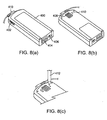
- FIG. 8(a) shows a perspective view of an adapter 400 according to an embodiment of the invention.
- the adapter 400 comprises a USB port 402, as well as a wall input cable port 404 and an auto/air input cable port 406.
- a cable 410 is also coupled to the adapter 400.
- FIG. 8(b) shows the underside of the power adapter 400 shown in FIG. 8(b) .
- a color coded selector 408 and a color coded selector button 410 are shown.
- the user may use a pen 412 to press the selector button 412 and at the same time may slide the color-coded selector button 410 to match the color code for the user's computer.
- the user will not inadvertently select the incorrect voltage by inadvertent movement of the color-coded selector button 410.
- the user may then try various connectors (which may be in the form of connector tips) and may connect them to the output connector coupled to the adapter 400 and to the user's computer.
- the selected connector may be color coded “blue” and the output connector may have an LED that glows “blue” so that the user can easily verify that the correct voltage will be supplied to his computer.
- FIG. 9 shows an output connector 466 and a computer 460 with a power port 462.
- a connectable connector 464 is removably connectable to both the output connector 466 and the power port 462.
- FIG. 10 shows two connectable connectors 464(a), 464(b) coupleable to an output connector 466.
- the output connector 466 also comprises band 470 which can provide light from the previously described blue and green LEDs.
- the connectors 464(a), 464(b) may have blue and green indicators 488(a), 488(b), respectively, so that the user knows which connector to use.
- the band 470 glows green, the user can use the connector with the green indicator.
- the band 470 glows blue, the user can select the connector with the blue indicator. By using matching colors, it is unlikely that the user will use the incorrect connector and output the incorrect voltage.
- embodiments of the invention may be include manipulating a switch in a power circuit to a first state to generate a first output voltage, where the power circuit is capable of generating a second output voltage when the switch is in a second state.
- An output connector is coupled to the power circuit and outputs the first output voltage using at least a first electrical contact and a second electrical contact.
- the consumer can then view an output (e.g., a visual output) from a voltage output indicator device coupled to the first and second electrical contacts.
- the output indicates that the power circuit is producing the first output voltage.
- the user can then select a first connector comprising an indicator which matches the output from the voltage indicator device, and then attach the first connector to the output connector.
- a power circuit comprising a switch is formed using conventional power supply manufacturing processes.
- the power circuit is adapted to generate a first output voltage and a second output voltage, depending on the state of the switch.
- An output connector can be attached to the power circuit.
- the output connector includes a plurality of electrical contacts including a first electrical contact and a second electrical contact.
- a voltage output indicator device is attached to the first and second electrical contacts. The voltage output indicates that the power circuit is producing the first output voltage or the second output voltage.
- Embodiments of the invention have a number of advantages. As noted above, no feedback signal is sent from the connectors to the power supply circuit. Accordingly, the power circuit need not have a programmed IC chip that is adapted to change the output voltage in response to the connector tip that is used. Omitting such programmed chips reduces the cost of the power supply systems. In addition, since a single connector tip or connector can be used with many different notebook computers in embodiments of the invention, fewer connector tips or connectors are needed in embodiments of the invention, thus simplifying the system as compared to conventional universal power supply systems.
- circuit implementations are shown in the foregoing Figures, it is understood that any suitable circuit implementation may be used to accomplish the end result of providing at least two conductive contacts in an output connector that can be used to provide different voltages to power different electronic devices.
- a power supply system may have an output connector that may be configured to interface or mate with three, four, five, six, or more connector tips or connectors.
Description
- This patent application is a non-provisional of and claims the benefit of the filing date of
U.S. Provisional Patent Application No. 60/796,117, filed on April 28, 2006 - Today, various electronic devices exist. Such electronic devices include cellular phones, portable computers, MP3 players, personal digital assistants (PDAs), etc. A person may own one or all of such portable electronic devices and each portable electronic device may have a separate power supply system associated with it. The use of many different power supplies is not desirable, since power supplies (sometimes called "power bricks") are often very bulky and cumbersome. For example, if a person owns a portable computer, a cellular phone, and an MP3 player, that person would also own three portable power supplies for those three portable electronic devices. If that person is traveling, it is quite cumbersome for that person to carry all of those portable power supplies with him.
- In response to this need, some have developed "universal" power supplies. One such power supply is described in
U.S. Patent No. 5,838,554 . This patent describes the use of a single power adapter for use with a plurality of different tips which can connect to different types of portable electronic devices. Each tip includes a different electrical component in it. In use, a tip is connected to the power adapter. The circuitry in the power adapter senses the electrical component in the tip and a feedback signal is provided to power circuitry containing a programmed IC chip. The power circuitry, in turn, provides a first output voltage. If a second tip with a different electrical component is selected, a different feedback signal is sent to the power circuitry and the power circuitry then produces a second output voltage associated with the second tip. - Although systems like the one described in
U.S. Patent No. 5,838,554 are effective in some instances, they could be improved. For example, the feedback circuitry that is used in such systems is complex and is relatively expensive to produce. The use of the above-described IC chip increases the cost of such power supplies. -
US 2005/021982 A1 discloses a power converter with output voltage level indicating device. The power converter is adapted to provide more than two output voltages and these voltages are supplied independent from a state of a switch. -
US 2005/259456 A1 discloses a power supply device having a number of voltages being permanently supplied at an output connector terminal with a total of five electrical contacts. -
US 2002 0043942 discloses a multiple output power adapter, wherein a first or a second output voltage can be supplied by an output connector. - What is desired is a simpler, more cost effective universal power supply solution. Embodiments of the invention address these and other problems, collectively and individually.
- Embodiments of the invention are directed to power supply systems and methods for using power supply systems according to the appended claims.
- These embodiments of the invention are described in further detail below.
-
-
FIG. 1(a) shows a perspective view of a power supply system according to an embodiment of the invention. -
FIG. 1(b) shows connection apparatus including an input connector. -
FIGS. 2(a)-2(c) show perspective views of connector tips according to embodiments of the invention.FIGS. 2(b) and 2(c) show invisible lines showing electrical contacts that are capable of coupling to electrical contacts in a common output connector. -
FIGS. 3(a)-3(b) show end views of connector tips, showing different contacts. -
FIG. 4 shows a block diagram of a power circuit for an AC to DC converter. -
FIG. 5 shows a block diagram of a power circuit for a DC to DC converter. -
FIG. 6(a) shows a block diagram of a power circuit according to another embodiment of the invention. -
FIGS. 6(b) and 6(c) respectively show schematic diagrams of first and second connectors and a portion of the circuit shown inFIG. 6(a) . -
FIG. 7(a) shows a block diagram of another power circuit and an output connector. -
FIGS. 7(b) and 7(c) show schematic diagrams of first and second connectors according to another embodiment of the invention. -
FIG. 7(d) shows a diagram of a system including a DC to DC converter. -
FIGS. 8(a) and 8(b) respectively show top perspective and bottom perspective views of a power adapter according to an embodiment of the invention. -
FIG. 8(c) shows a bottom perspective view of the power adapter shown nFIG. 8(b) when it is changing states. -
FIG. 9 shows a system including a cable end, a connector, and a portable electronic device such as a portable computer. -
FIGS. 10(a) and 10(b) show perspective views of first and second connectors coupled to the end of a cable connector. - Embodiments of the invention are directed to power supply systems. An exemplary power supply system comprises a power adapter which may house a power circuit. The power circuit may output a plurality of voltages (e.g., 16 VDC or 19.5 VDC). The voltages may be output simultaneously from the power circuit or may be output independently from the power circuit depending on the state of an external switch. Various connectable connectors such as connector tips can be mechanically and electrically coupled to an output connector in the power adapter. The various connectable connectors may be used with different electronic devices.
- Any suitable type of electronic device can be powered by the power supply systems according to embodiments of the invention. Examples of electronic devices comprise notebook computers, cell phones, MP3 players, televisions, etc.
- The output connector coupled to the power circuit, and the connectable connectors that are connectable to the output connector may have any suitable shape and/or configuration. Each connectable connector may be cooperatively structured with the output connector so that it can be easily connected to and separated from the output connector. For example, the output connector may be a female type connector, and may mechanically mate with male-type first and second connectable connectors (or vice versa). Each connectable connector and each output connector can also have a plurality of electrical conductors with corresponding electrical contacts.
- The connectable connectors may be in any suitable form. For example, connectable connectors may be in the form of connector tips, connector wires, connection apparatuses, etc. A preferred connectable connector may be in the form of a connector tip, which would be in between the power adapter and the electronic device being powered.
- As noted above, conventional power adapters require some method of feedback from the tip to the power circuit to cause it to output a particular voltage. Embodiments of the invention do not require this. In embodiments of the invention, a power circuit in a power supply system outputs a plurality of voltages (e.g., two voltages - 16V and 19V), and the selection of a connector tip or the like can determine which voltage will be ultimately output. The power circuit in the power supply system may also output different voltages depending on the state of a power switch. The connector tips can be used to charge electronic devices such as notebook computers.
- It has been determined that a universal power supply can output at least two discrete voltages of about +16VDC (+/- 1 or 2 Volts) and about +19.5VDC (+/- 1 or 2 Volts) and can be used to provide power to most notebook computers on the market today. In preferred embodiments, the power circuit in the power supply is adapted to provide only two discrete voltages to simplify the design of the power supply and power circuit. Although a notebook computer may be designed to work with a specific input voltage such as 20 V, it has been determined that the notebook computer may tolerate a slight deviation from 20V. The typical deviation could be +/- 1 or 2 Volts. Therefore, if a universal power supply could use a connector tip to output 19.5 VDC, it would be able to supply power to notebook computers that are designed to accept 19 V, 19.5 V, and 20V. Thus, one connector tip type may be provided to provide power to a number of brands of notebook computers, instead of one brand of notebook computers as long as the mechanical tip type can fit into the power ports of such notebook computers. Current universal power supplies may have as many as 37 connector tips that work with a single power brick. Having too many connector tips can be cumbersome as well as confusing. Having too many connector tips with too may different voltage ratings can also increase the chances that the consumer may use the incorrect one and damage his notebook computer. Too many connector tips with too many different voltages may also increase the overall cost of the universal power supply system.
- In preferred embodiments, there can be two (or more) connector tip types that can connect to the output connector coupled to a power circuit configured to generate at least two discrete voltages. The connector tip types would respectively output about +16 VDC and about +19.5 VDC when connected to the output connector. The connector tip types would be compatible with most commercially available notebook computers. For example, a first connector tip type may provide an output voltage at about 19.5 V when connected to the output connector and may have relative dimensions (OD/ID) of 4.75/1.7, 5.5/1.7, 5.5/2.1, 5.5/2.5, 6/1.4, 7.4/0.6 corresponding to 6 connector tips. A second connector tip type may output a voltage of 16V when connected to the output connector and may have relative dimensions (OD/ID) of 5.5/2.5, 6/1.4, 6.3/3 corresponding to 3 connector tips. Thus, in an exemplary power supply system according to an embodiment of the invention, there can be (i) a power adapter comprising a power circuit and an output connector, (ii) a first type of connector tip and multiple physical configurations of that first type of connector tip, and (ii) a second type of connector tip and multiple physical configurations of that second type of connector tip.
- To enable the power supply system to charge multiple devices and/or low powered devices, the power adapter can include a low powered female USB port (at least one) on the body of the adapter or a combination of ports (e.g., a female USB port and a female FireWire port). The ports can be selected based on available/common charging cables for devices.
- In one embodiment of the invention, the power supply system comprises a power circuit adapted to generate a first output voltage and a second output voltage at the same time, and an output connector coupled to the power circuit. The output connector includes a plurality of electrical contacts including a first set of contacts adapted to provide the first output voltage and a second set of electrical contacts adapted to provide the second - output voltage at the same time as the first output voltage. The first and second sets of contacts are different. A first connector (e.g., a first connector tip) can be configured to connect to the output connector and electrically couple to the first set of contacts to provide the first output voltage to a first electronic device (e.g., a portable computer made by manufacturer A). Alternatively, a second connector (e.g., a second connector tip) can be configured to connect to the output connector and electrically couple to the second set of contacts to provide the second output voltage to a second electronic device (e.g., a portable computer made by manufacture B).
- In a specific example, there can be three conductive contacts in an output connector that is coupled to the power circuit. The three conductive contacts could have the values: GND, +16VDC, and +19VDC. In preferred embodiments, the different output voltages that can be provided by the contacts in the output connector can range from about 15-17 VDC (or 14-17 VDC) for a first connector, and about 18-20 VDC (or 17-21 VDC) for a second connector.
- Unlike conventional universal power supplies, in this embodiment of the invention, the connectable connector does not have an electrical component that provides feedback to a power circuit to cause the power circuit to generate a specific voltage. Rather, in this embodiment of the invention, the voltages are always available and the voltage output that is ultimately provided by the power supply system depends on the connectable connector that is connected to the output connector that is coupled to the power circuit.
- If the connectable connectors in the power supply system are connector tips, each connector tip can act as a jumper to different sets of contacts in the output connector to output the correct voltage. For example, the output connector can have a plurality of electrical contacts including contacts A, B, and C. The first connector tip may have contacts that connect to a first set of contacts A and B in the output connector to produce a first output voltage associated with a first electronic device. A second connector tip may have contacts that connect to a second set of contacts A and C in the output connector to produce a second output voltage associated with a second electronic device. Although two connector tips and three electrical contacts in an output connector are described in detail, more than two connector tips and more than three electrical contacts in an output connector can be used in other embodiments of the invention.
-
FIG. 1(a) shows apower supply system 100 according to an embodiment of the invention. Thepower supply system 100 includes apower adapter 10 including a casing (e.g., a plastic casing) 10(a) and an optional auxiliary connector port 10(b) in the casing. A wire 28 (or cable) couples anoutput connector 30 to thepower adapter 10. Thepower adapter 10 may include power supply components and/or power circuit components including transformers, rectifiers, inverters, etc. Anotherwire 24 couples aninput connector 20 to thepower adapter 10. Theinput connector 20 may be a household plug that plugs into an AC power source. Alternatively, theinput connector 20 may be a plug (e.g., a cigarette lighter plug) that plugs into a DC power source. - The
power supply system 100 may also include afirst connector 32, which may be in the form of connector tip. Theconnector 32 may include a body portion 32(a) that is configured to mate with theoutput connector 30, and a mating portion 32(b) which mates with a port of a first electronic device (not shown). Thefirst connector 32 may also have electrical contacts that electrically couple to only a certain set of electrical contacts (e.g., contacts A and B) in a plurality of contacts (e.g., contacts A, B, and C) in theoutput connector 30. - The
power supply system 100 may also include asecond connector 33, which may be in the form of connector tip. Thesecond connector 33 may include a body portion 33(a) that is configured to mate with theoutput connector 30 when thefirst connector 32 is not used. Thesecond connector 33 may also include a mating portion 33(b) which mates with a port of a second electronic device (not shown). Thesecond connector 33 may also have electrical contacts that electrically couple to only a certain set of electrical contacts (e.g., contacts A and C) in a plurality of contacts (e.g., contacts A, B, and C) in theoutput connector 30. - In
FIG. 1(a) , the mating portions 32(b), 33(b) of therespective connectors respective connectors output connector 30. In embodiments of the invention, some members of the sets may be the same in some cases, but the sets are different. For example, if theoutput connector 30 has contacts A, B, and C, then a first connector may have corresponding connectors A and B, while a second connector may have corresponding contacts A and C. In this example, the sets of contacts (i.e., A-B, and A-C) are different, yet they have one common member A. In other embodiments, it is not necessary for the sets to have at least one common member. -
FIG. 1(b) shows anauxiliary connection device 50, which includes anauxiliary connector 52 including a body portion 52(a) and a mating portion 52(b). The mating portion 52(b) can be a plug which can plug into the auxiliary connector port 10(b) in thepower adapter 10 shown inFIG. 1(a) . Anotherconnector 54 including a body portion 54(a) and a connector portion 54(b) may be coupled to theauxiliary connector 52 via awire 58. Theauxiliary connection device 50 can provide low voltages to low voltages devices such as cell phones, while theconnectors FIG. 1(a) can provide higher voltages to higher voltage devices such as notebook computers. -
FIG. 2(a) shows aconnector 60 in the form of a connector tip. Theconnector 60 includes a body portion 60(a) comprising plastic and a mating portion 60(b) comprising electrical contacts. -
FIG. 2(b) shows a first connector including electrical contacts 60(c), 60(d), which would connect to corresponding contacts in an output connector (not shown) to provide a first output voltage. -
FIG. 2(c) shows a second connector including electrical contacts 60(c) and 60(e), which would connect to corresponding contacts in an output connector (not shown) to provide a second output voltage.FIGS. 3(a) and 3(b) show end views of the connectors shown inFIGS. 2(b) and 2(c) . - Other embodiments of the invention are also possible. For example, instead of a connector tip being detachable from an output connector coupled to a cable, the cable can be completely detachable from an adapter body (e.g., the "brick") and the connector tip may be a permanent part of the cable. The connector between the cable and adapter body uses the method described above to output one of the available voltages from a single output connector. In another embodiment, the adapter body can provide output voltage contacts that are covered by a slide, such that the user would have to move the slide to one side to expose either the 16 VDC or 19 VDC contact in the output connector. By selecting one contact, the other is rendered useless by the slide which covers the unselected contact.
- The power supply system described above can be used in any suitable manner. For example, a user may first obtain the above-described power supply system. Then, the user may look on a chart or the like (an example of a chart is provided below), to match his first electronic device (e.g., a notebook computer) to a first connectable connector (e.g., a connector tip). The consumer may thereafter connect the first connectable connector to the output connector coupled to the above-described power circuit. The connected first connector will then output a specific voltage (e.g., 16 VDC), even though the power circuit in the power adapter and the output connector coupled to the power circuit are outputting a plurality of voltages. If the consumer has a second electronic device that operates at a different voltage than the first electronic device, then the user may detach the first connector from the output connector and may then attach the second connector to the output connector and the second electronic device to power the second electronic device.
- Exemplary power circuits that can be used with the embodiments described above with respect to
FIGS. 1-3 are described inFIGS. 4-5 . -
FIG. 4 shows a block diagram of a power circuit according to an embodiment of the invention. The power circuit converts AC power, for example from a wall socket, to DC power that may be used to power a portable device. As shown, there is one AC input and there are two DC outputs. The power circuit includes anAC input line 78, which provides an AC voltage (e.g., 100-240 VAC) to a rectifier and anoptional filter 80. The rectifier and filter 80 changes the AC input voltage to a DC output voltage (e.g., 50-120 VDC). The DC output voltage is then fed to aninverter 82, which generates an AC signal (e.g., 20 kHz at 50-120 VAC) that is stepped down in voltage by a transformer 84 (e.g., 20-60 VAC). The stepped-down AC voltage is then sent to another rectifier andoptional filter combination 86, where the AC voltage is changed to a DC voltage (e.g., 25-60 VDC). The DC voltage is then fed todifferent regulators contacts regulators Feedback lines inverter 82 to regulate the output voltages. - As explained above, a first connector tip that is configured to deliver 19.5 VDC to an electronic device (such as a computer) may have contacts that electrically couple to the 19.5 VDC contact and to a ground contact (not shown). A second connector tip that is configured to deliver 16 VDC to another type of electronic device (or different brand of computer) may have contacts that electrically couple to the 16 VDC contact and to the ground contact.
-
FIG. 5 shows a DC to DC power supply circuit for a DC to DC power supply system. As shown, the power circuit may include a DC input line 96 (e.g., 11-16 VDC) which receives a DC voltage from a DC source (e.g., from a car cigarette lighter socket). A DC-DC converter 98 receives the DC voltage from theDC input line 96, and this DC voltage may be fed to theappropriate voltage regulators contacts Feedback lines DC converter 98 to regulate the voltages provided to theregulators - In other embodiments, a combination AC to DC and DC to DC converter may be created by combining the power circuits shown in
FIGS. 4 and5 . One way of doing this would be to provide for a power adapter that includes the circuits inFIGS. 4 and5 . Each circuit could have its own input connector and its own output connector. Another way of creating a combined AC to DC and DC to DC converter with a common output connector would be to electrically couple the 19.5VDC contacts VDC contacts - In other embodiments of the invention, a user may use a switch to cause a power circuit to output a desired voltage instead of having the power circuit output a plurality of voltages simultaneously. An example can be described with to
FIGS. 6(a)-6(c) . -
FIG. 6(a) shows a block diagram of a power circuit according to an embodiment of the invention. The power circuit converts AC power to DC power. The power circuit includes anAC input line 278, which provides an AC voltage (e.g., 100-240 VAC) to a rectifier and anoptional filter 280. TheAC input line 278 may receive AC voltage from an AC source such as a power outlet in a home. The rectifier and filter 280 changes the AC input voltage to a DC output voltage (e.g., 50-120 VDC). The DC output voltage is then fed to aninverter 282, which generates an AC voltage (e.g., 20 kHz at 50-120 VAC) that is stepped down by a transformer 284 (e.g., 20-60 VAC). The stepped-down AC voltage is then sent to another rectifier andoptional filter combination 286, where the AC voltage is converted to a DC voltage (e.g., 25-60 VDC). The DC voltage is then fed to avariable regulator 210 which produces output voltages atcontacts switch 218. A specific embodiment of the present invention provides output voltages of 19.5 VDC and 16 VDC, though in other embodiments other voltages may be provided. Afeedback line 216 provides a signal back to theinverter 282 to regulate the output voltages. - In this example, when an AC signal is input to
line 278, an output voltage of 16 VDC is provided at afirst contact 292 when theswitch 218 is open. The open state of theswitch 218 sends a signal to thevariable regulator 210 to cause thevariable regulator 210 to output a voltage of 16 VDC to only thefirst contact 292, without outputting a voltage of 19.5 VDC to thesecond contact 294. - As shown in
FIG. 6(b) , afirst connector 220 may have a body portion 220(a) and a mating portion 220(b). The body portion 220(a) may have two contacts 220(c), which are configured to mate or connect to the first andthird contacts output connector 299. The two contacts 220(c) and/or the mechanical configuration of the body portion 220(a) may be such that the contacts 220(c) cannot couple to thesecond contact 294 in theoutput connector 299. - Also in this example, when an AC signal is input to
line 278, an output voltage of 19 VDC is provided at asecond contact 294 when theswitch 218 is closed. The closed state of theswitch 218 sends a signal to thevariable regulator 210 to cause thevariable regulator 210 to output a voltage of 19 VDC to only thesecond contact 294, without outputting a voltage of 16 VDC to thefirst contact 292. - As shown in
FIG. 6(c) , asecond connector 222 may have a body portion 222(a) and a mating portion 222(b). The body portion 222(a) may have two contacts 222(c), which are configured to mate or connect to the second andthird contacts output connector 299. The two contacts 222(c) and/or the mechanical configuration of the body portion 222(a) may be such that the contacts 222(c) cannot couple to thefirst contact 292 in the output connector. - To assist the user in selecting the correct connector, connector indicators such as numbers, colors, letters, etc., could be placed on the
connectors switch 218 so that the indicators indicate to the user which connector corresponds to which switch position. For example, the "off position" of theswitch 218 may be associated with a blue label and thefirst connector 220 may have a corresponding blue label. The "on position" of theswitch 218 may be associated with a green label and thesecond connector 222 may have a corresponding green label. A chart or other information medium may be used to inform the user as to which color is associated with his portable consumer device. Using such color codes (or other indicators), the user will know whichconnector switch 218. - The embodiments described with respect to
FIGS. 6(a)-6(c) have a number of additional advantages. In the embodiments described with respect toFIGS. 6(a)-6(c) , it is highly unlikely that a user would use the wrong connector with his portable consumer device and consequently damage his portable consumer device. For example, to potentially damage his portable consumer device, the consumer would need to select the incorrect switch position, and also select the incorrect connector. If the consumer selects the incorrect switch position, but the correct connector, then the power supply would output 0 Volts. For example, referring toFIGS. 6(b) and 6(c) , the user may have a computer that is powered by 16 VDC. The user may incorrectly close theswitch 218 as shown inFIG. 6(c) and may incorrectly select a 19 VDC output. If the user selects thecorrect connector 220 that is associated with a 16 VDC output as shown inFIG. 6(b) , and mechanically couples it to theoutput connector 299, then the output of theconnector 220 would be 0 Volts, since the contacts 220(c) would not be coupled to the live 19VDC contact 294. Thus, the user would not inadvertently supply the incorrect voltage to his computer. The embodiments shown inFIGS. 6(a)-6(c) are much safer for the consumer to use and make it more likely that the user will not inadvertently provide the wrong output voltage to his computer. - The embodiments described with respect to
FIGS. 6(a)-6(c) specifically relate to an AC to DC power supply system. It is understood that the same general principles may apply to a DC to DC power supply system (as described above with respect toFIG. 5 ) and a combination AC to DC and DC to DC power supply system (as described above). For example, the DC to DC converter shown inFIG. 5 can be modified with one or more switches to open and close the circuits including the 16 VDC and 19.5 VDC contacts. - Other embodiments of the invention can be described with reference to
FIGS. 7(a)-7(c) . These embodiments can use a voltage output indicator device to indicate the voltage that is being output by the power circuit in the power adapter. Using the indicator device, the user can be certain that he has selected the correct voltage. -
FIG. 7(a) shows a block diagram of a power circuit according to an embodiment of the invention. The power circuit converts AC power to DC power. The power circuit includes anAC input line 378, which provides an AC voltage (e.g., 100-240 VAC) to a rectifier and anoptional filter 380. TheAC input line 378 may receive an AC voltage from an AC source such as a power outlet in a home. The rectifier and filter 380 changes the AC input voltage to a DC output voltage (e.g., 50-120 VDC). The DC output voltage is then fed to aninverter 382, which generates an AC voltage (e.g., 20 kHz at 50-120 VAC) that is stepped down by a transformer 384 (e.g., 20-60 VAC). The stepped-down AC signal is then sent to another rectifier and optional filter combination 386, where the AC voltage is changed to a DC voltage (e.g., 25-60 VDC). The DC voltage is then fed to avariable regulator 310 which produces output voltages atcontacts switch 218. A specific embodiment of the present invention provides output voltages of 19.5 VDC and 16 VDC, though other embodiments of the present invention may provide other output voltages. Afeedback line 316 provides a signal back to theinverter 382 to regulate the output voltages. - In this embodiment, there are two
output contacts variable regulator 310, instead of three as in the embodiments described above with reference toFIGS. 6(a)-6(c) . The twooutput contacts ground contact 391 and apositive voltage contact 392. The state of the positive voltage contact can be 16 or 19.5 volts, depending upon the state of theswitch 218. For example, if theswitch 218 is closed, then the output voltage may be 16 VDC. If theswitch 218 is open, then the output voltage may be 19.5 VDC. Although theswitch 218 has two discrete states in this example, it is understood that it may have more than two discrete states in other examples. - The power supply system may also comprise a voltage
output indicator device 259. In this example, the voltageoutput indicator device 259 comprises a sense element 332 such as a chip, and lighting elements such as LEDs. Referring toFIG. 7(a) , the sense element 332 may be electrically coupled to thecontacts contact 392, and may cause a blue LED 352(a) to light up if the voltage of thecontact 392 is at 16 VDC and may cause a green LED 352(b) to light up if the voltage of thecontact 392 is at 19.5 VDC. At least part (e.g., the LEDs) of the voltageoutput indicator device 259 is in theoutput connector 255, to help the user select the correct connectable connector. - As shown in
FIGS. 7(b) and 7(c) , twoconnectors output connector 255 containing thecontacts connector contacts output connector 255. Eachconnector indicator - To choose the correct state of the
switch 218 and consequently the correct voltage, the user may look on a chart which shows his computer and may match, for example, the color blue to his computer if his computer will accept 16 VDC. An example of such a chart is shown below. As shown, there can be a column for a computer manufacturer, the indicator state (color code) associated with the manufacturer's computers, the voltage range accepted by the manufacturer's computers, and possible connectors (e.g., identified by letter) that can be used with the manufacturer's computers.Computer Manufacturer Color Code Voltage Try This Connector Manufacturer A Green 17-21V D, H Manufacturer B Green 17-21V E, H, I Manufacturer C Blue 14-17V H, J - After the user identifies the color associated with his computer, the user may then select the position on the
switch 218 which may be associated with the selected color (e.g., blue). After the user manipulates theswitch 218, the user may look at theblue indicator 344 on theconnector 324 and may then couple the conductors 324(c) in theconnector 324 to thecontacts output connector 255. - By using LEDs with different colors, the user has a reference to what the output voltage the power adapter is producing at any moment. For safety purposes, the user can check to see if there is agreement between the connectable connector color, the LED color in the output connector, and switch color before plugging the power supply connector into his computer.
- The embodiments described with respect to
FIG. 7(a) specifically relate to a AC to DC power supply system. It is understood that the same general principles may apply to a DC to DC power supply system (as described above with respect toFIG. 5 ) and a combination AC to DC and DC to DC power supply system (as described above). For example, referring toFIG. 7(d) , a DC to DC circuit may comprise a DC toDC converter 240 and avariable regulator 242 coupled to the DC toDC converter 240. Anoutput connector 255 may be coupled to thevariable regulator 242. The illustrated components in theconnector 255 are described above with respect toFIG. 7(a) , and the descriptions of those components need not be repeated here. An external switch 318 may be coupled to thevariable regulator 242 to adjust the voltage output by thevariable regulator 242. A feedback loop 244 may send a signal back to the DC toDC converter 240 to regulate the voltage output by the DC toDC converter 240. -
FIG. 8(a) shows a perspective view of anadapter 400 according to an embodiment of the invention. Theadapter 400 comprises aUSB port 402, as well as a wallinput cable port 404 and an auto/airinput cable port 406. Acable 410 is also coupled to theadapter 400. -
FIG. 8(b) shows the underside of thepower adapter 400 shown inFIG. 8(b) . A color codedselector 408 and a color codedselector button 410 are shown. - As shown in
FIG. 8(c) , to set up theadapter 400, the user may use apen 412 to press theselector button 412 and at the same time may slide the color-codedselector button 410 to match the color code for the user's computer. By using thepen 412 andselector button 412, the user will not inadvertently select the incorrect voltage by inadvertent movement of the color-codedselector button 410. - The user may then try various connectors (which may be in the form of connector tips) and may connect them to the output connector coupled to the
adapter 400 and to the user's computer. As noted above, the selected connector may be color coded "blue" and the output connector may have an LED that glows "blue" so that the user can easily verify that the correct voltage will be supplied to his computer. -
FIG. 9 shows anoutput connector 466 and acomputer 460 with apower port 462. Aconnectable connector 464 is removably connectable to both theoutput connector 466 and thepower port 462. -
FIG. 10 shows two connectable connectors 464(a), 464(b) coupleable to anoutput connector 466. Theoutput connector 466 also comprisesband 470 which can provide light from the previously described blue and green LEDs. The connectors 464(a), 464(b) may have blue and green indicators 488(a), 488(b), respectively, so that the user knows which connector to use. As explained above, when theband 470 glows green, the user can use the connector with the green indicator. When theband 470 glows blue, the user can select the connector with the blue indicator. By using matching colors, it is unlikely that the user will use the incorrect connector and output the incorrect voltage. - Thus, as illustrated above, embodiments of the invention may be include manipulating a switch in a power circuit to a first state to generate a first output voltage, where the power circuit is capable of generating a second output voltage when the switch is in a second state. An output connector is coupled to the power circuit and outputs the first output voltage using at least a first electrical contact and a second electrical contact. The consumer can then view an output (e.g., a visual output) from a voltage output indicator device coupled to the first and second electrical contacts. The output indicates that the power circuit is producing the first output voltage. The user can then select a first connector comprising an indicator which matches the output from the voltage indicator device, and then attach the first connector to the output connector.
- The above-described embodiments may be formed using any suitable methods. For example, in some embodiments, a power circuit comprising a switch is formed using conventional power supply manufacturing processes. The power circuit is adapted to generate a first output voltage and a second output voltage, depending on the state of the switch. An output connector can be attached to the power circuit. The output connector includes a plurality of electrical contacts including a first electrical contact and a second electrical contact. A voltage output indicator device is attached to the first and second electrical contacts. The voltage output indicates that the power circuit is producing the first output voltage or the second output voltage.
- Embodiments of the invention have a number of advantages. As noted above, no feedback signal is sent from the connectors to the power supply circuit. Accordingly, the power circuit need not have a programmed IC chip that is adapted to change the output voltage in response to the connector tip that is used. Omitting such programmed chips reduces the cost of the power supply systems. In addition, since a single connector tip or connector can be used with many different notebook computers in embodiments of the invention, fewer connector tips or connectors are needed in embodiments of the invention, thus simplifying the system as compared to conventional universal power supply systems.
- Although specific circuit implementations are shown in the foregoing Figures, it is understood that any suitable circuit implementation may be used to accomplish the end result of providing at least two conductive contacts in an output connector that can be used to provide different voltages to power different electronic devices.
- Although much of the description above refers to two connector tips and three electrical contacts in an output connector, embodiments of the invention may include any number of connector tips, or connectors, and any number of electrical contacts in an output connector. For example, a power supply system according to an embodiment of the invention may have an output connector that may be configured to interface or mate with three, four, five, six, or more connector tips or connectors.
- The above description is illustrative and is not restrictive. Many variations of the invention will become apparent to those skilled in the art upon review of the disclosure. The scope of the invention should, therefore, be determined not with reference to the above description, but instead should be determined with reference to the pending claims along with their full scope or equivalents.
- One or more features from any embodiment may be combined with one or more features of any other embodiment without departing from the scope of the invention.
- A recitation of "a", "an" or "the" is intended to mean "one or more" unless specifically indicated to the contrary. In addition, words such as "over", "under", etc. are used to described features as they are shown in the Figures and may or may not refer to absolute positions.
Claims (15)
- A power supply system (100) comprising:a power circuit comprising a switch and adapted to generate a first output voltage or a second output voltage, depending on a state of the switch:an output connector (30) coupled to the power circuit, wherein the output connector includes a plurality of electrical contacts comprising a first electrical contact and a second electrical contact;a first connector (32) capable of being detachably coupled to the output connector; anda second connector (33) capable of being detachably coupled to the output connector,wherein the first and second connectors are also capable of coupling to and supplying power to different electronic devices, and that the power circuit is adapted to provide only the first output voltage or the second output voltage through the output connector, wherein the first output voltage is about 16 V and the second output voltage is about 19 V.
- The power supply system of claim 1 wherein the first connector includes a first indicator and the second connector includes a second indicator.
- The power supply system of claim 2 wherein the first indicator corresponds to a third indicator proximate to a first switch position and the second indicator corresponds to a fourth indicator proximate to a second switch position.
- The power supply system of claim 3 wherein the first indicator is a first color and the second indicator is a second color, wherein the third indicator includes the first color and the fourth indicator includes the second color.
- The power supply system of claim 1 further comprising a USB port coupled to the power circuit.
- The power supply system of claim 1 wherein the power circuit includes an AC to DC conversion circuit.
- The power supply system of claim 1 wherein the power circuit includes a DC to DC conversion circuit.
- A power supply system according to claim 1, further comprising:a voltage output indicator device coupled to the first and second electrical contacts, wherein the voltage output indicator device indicates that the power circuit is producing the first output voltage or the second output voltage.
- The power supply system of claim 8 wherein the voltage output indicator device comprises at least one sense element and at least one light element.
- The power supply system of claim 8 wherein the system comprises a first indicator associated with a first switch position and a second indicator associated with a second switch position, the first indicator also being on the first connector, and the second indicator being on the second connector.
- The power supply system of claim 10 wherein the first indicator is a first color and the second indicator is a second color.
- A method comprising:manipulating a switch in a power circuit to a first state to generate a first output voltage, wherein the power circuit is capable of generating a second output voltage when the switch is in a second state, wherein an out-put connector (30) is coupled to the power circuit and comprises a first electrical contact and a second electrical contact;viewing an output from a voltage output indicator device coupled to the first and second electrical contacts, wherein the voltage output indicator device indicates that the power circuit is producing the first output voltage; andselecting a first connector (32) comprising an indicator which matches the output from the voltage indicator device; andattaching the first connector to the output connector,wherein a second connector (33) is capable of being detachably coupled to the output connector, and wherein the first and second connectors are also capable of being coupled to different electronic devices to supply power to the different electronic devices,wherein the power circuit is adapted to provide only the first output voltage or the second output voltage through the output connector, and wherein the first output voltage is about 16 V and the second output voltage is about 19 V.
- The method of claim 12 further comprising connecting the first connector to a power port in a portable electronic device.
- The method of claim 12 wherein the voltage output indicator device com-prises LEDS with different colors.
- The method of claim 12 wherein the indicator comprises a color.
Priority Applications (1)
| Application Number | Priority Date | Filing Date | Title |
|---|---|---|---|
| EP20140153068 EP2731226A3 (en) | 2006-04-28 | 2007-04-17 | Power supply system |
Applications Claiming Priority (3)
| Application Number | Priority Date | Filing Date | Title |
|---|---|---|---|
| US79611706P | 2006-04-28 | 2006-04-28 | |
| US11/690,068 US7642671B2 (en) | 2006-04-28 | 2007-03-22 | Power supply system providing two output voltages |
| PCT/US2007/066784 WO2007143283A2 (en) | 2006-04-28 | 2007-04-17 | Power supply system |
Related Child Applications (2)
| Application Number | Title | Priority Date | Filing Date |
|---|---|---|---|
| EP20140153068 Division EP2731226A3 (en) | 2006-04-28 | 2007-04-17 | Power supply system |
| EP20140153068 Division-Into EP2731226A3 (en) | 2006-04-28 | 2007-04-17 | Power supply system |
Publications (3)
| Publication Number | Publication Date |
|---|---|
| EP2016659A2 EP2016659A2 (en) | 2009-01-21 |
| EP2016659A4 EP2016659A4 (en) | 2011-03-30 |
| EP2016659B1 true EP2016659B1 (en) | 2014-07-16 |
Family
ID=38685084
Family Applications (2)
| Application Number | Title | Priority Date | Filing Date |
|---|---|---|---|
| EP20070811849 Not-in-force EP2016659B1 (en) | 2006-04-28 | 2007-04-17 | Power supply system |
| EP20140153068 Withdrawn EP2731226A3 (en) | 2006-04-28 | 2007-04-17 | Power supply system |
Family Applications After (1)
| Application Number | Title | Priority Date | Filing Date |
|---|---|---|---|
| EP20140153068 Withdrawn EP2731226A3 (en) | 2006-04-28 | 2007-04-17 | Power supply system |
Country Status (6)
| Country | Link |
|---|---|
| US (2) | US7642671B2 (en) |
| EP (2) | EP2016659B1 (en) |
| CN (1) | CN101432943B (en) |
| CA (1) | CA2648058A1 (en) |
| TW (1) | TWI436572B (en) |
| WO (1) | WO2007143283A2 (en) |
Families Citing this family (39)
| Publication number | Priority date | Publication date | Assignee | Title |
|---|---|---|---|---|
| US9153960B2 (en) | 2004-01-15 | 2015-10-06 | Comarco Wireless Technologies, Inc. | Power supply equipment utilizing interchangeable tips to provide power and a data signal to electronic devices |
| US7500371B2 (en) | 2005-11-18 | 2009-03-10 | Acco Brands Usa Llc | Locking device with passage |
| US20110068733A1 (en) * | 2008-02-11 | 2011-03-24 | Paul Duda | Electronic vampire |
| US20100194197A1 (en) * | 2009-02-04 | 2010-08-05 | Kung-Neng Lee | Power converter with communication capability |
| US20110050170A1 (en) * | 2009-02-22 | 2011-03-03 | Eastlack Jeffrey R | Electromechanical Vampire Proof Battery Charger System |
| CN102334244B (en) * | 2009-02-26 | 2014-01-01 | 丰田自动车株式会社 | Plug conversion adapter |
| WO2010101657A2 (en) * | 2009-03-05 | 2010-09-10 | Vampire Labs, Llc | Electromechanical vampire proof battery charger |
| US8766476B2 (en) | 2009-10-02 | 2014-07-01 | Ramin Rostami | Apparatus and method for communicating data and power with electronic devices |
| DE212010000070U1 (en) * | 2009-05-29 | 2012-01-19 | Acco Brands, Inc. | Securing device comprising a fastener |
| US9118194B2 (en) | 2012-04-30 | 2015-08-25 | Foreign Trade Corporation | Configurable apparatus and methods for supplying power and data to electronic devices |
| US8169105B2 (en) * | 2009-07-12 | 2012-05-01 | Ramin Rostami | Configurable apparatus and methods for supplying power and data to electronic devices |
| US8354760B2 (en) * | 2009-10-28 | 2013-01-15 | Comarco Wireless Technologies, Inc. | Power supply equipment to simultaneously power multiple electronic device |
| CN102055349A (en) * | 2009-10-29 | 2011-05-11 | 瀚斯宝丽股份有限公司 | Power supply with heating function |
| US9715607B2 (en) | 2010-02-11 | 2017-07-25 | Advanced Wireless Innovations Llc | Apparatus and methods for communicating power and data with electronic devices |
| US20120068535A1 (en) * | 2010-09-20 | 2012-03-22 | Radioshack Corporation | Energy converter, and associated method, for providing converted energy to a set of electronic devices |
| US9614379B2 (en) * | 2011-03-23 | 2017-04-04 | Toyota Jidosha Kabushiki Kaisha | Adapter, and vehicle and method for performing power feeding using adapter |
| USD651889S1 (en) | 2011-04-19 | 2012-01-10 | Acco Brands Usa Llc | Security apparatus |
| TWI454027B (en) * | 2011-09-16 | 2014-09-21 | Phihong Technology Co Ltd | Combinative power device |
| US8568152B1 (en) | 2012-04-19 | 2013-10-29 | Pass & Seymour, Inc. | Shutter assembly for electrical devices |
| US8550827B1 (en) | 2012-07-25 | 2013-10-08 | Targus Group International, Inc. | Multi-sleeve power tips |
| US8821199B2 (en) | 2012-07-25 | 2014-09-02 | Targus Group International, Inc. | Multi-prong power tip adaptor |
| US9153914B2 (en) * | 2012-08-17 | 2015-10-06 | Advanced Charging Technologies, LLC | Power device having multiple modes of operation |
| CN103683905A (en) * | 2012-09-07 | 2014-03-26 | 鸿富锦精密工业(深圳)有限公司 | Voltage converter |
| CA2910800C (en) * | 2013-06-03 | 2016-10-11 | Norman R. Byrne | Low voltage power receptacle |
| US9257893B2 (en) | 2013-07-29 | 2016-02-09 | City University Of Hong Kong | USB power supply |
| US9496726B2 (en) | 2013-07-31 | 2016-11-15 | Leviton Manufacturing Co., Inc. | Multiport USB charger |
| DE102013221588A1 (en) | 2013-10-24 | 2015-05-13 | Robert Bosch Gmbh | Connector comprising at least one signal generator |
| BR102015011128A2 (en) | 2014-05-19 | 2017-11-28 | R. Byrne Norman | BRANCHED ELECTRIC SYSTEM AND HIGH SEAT DENSITY AREA |
| US20170033566A1 (en) * | 2015-07-27 | 2017-02-02 | Gibson Brands, Inc. | Remote power source with variable voltage output sources |
| CA3016630A1 (en) * | 2016-03-21 | 2017-09-28 | Mobile Electronics Inc. | Method and system for a universal programmable voltage module |
| WO2018067616A1 (en) | 2016-10-04 | 2018-04-12 | Roys Curtis Alan | Electrical wall receptacle, led module, and lamp system |
| US10425236B2 (en) | 2016-10-05 | 2019-09-24 | Norman R. Byrne | Intelligent electrical power distribution system |
| CN109923778B (en) | 2016-10-07 | 2020-11-10 | 诺曼·R·伯恩 | Robust weather resistant power distribution |
| CN106648004A (en) * | 2016-10-14 | 2017-05-10 | 柳州译海网络科技有限公司 | Universal computer power line |
| CN106410549A (en) * | 2016-10-14 | 2017-02-15 | 柳州译海网络科技有限公司 | Heat-resistant general computer power supply wire |
| TWI695553B (en) | 2019-05-08 | 2020-06-01 | 群光電能科技股份有限公司 | Plug, power supply and power connector |
| CA3081864A1 (en) | 2019-05-28 | 2020-11-28 | Norman R. Byrne | Modular electrical system |
| CA3082616A1 (en) | 2019-06-07 | 2020-12-07 | Norman R. Byrne | Electrical power distribution system |
| CN114034979A (en) * | 2021-11-12 | 2022-02-11 | 昆明理工大学 | Alternating current transmission line distance measuring method and system |
Family Cites Families (178)
| Publication number | Priority date | Publication date | Assignee | Title |
|---|---|---|---|---|
| US3714452A (en) | 1972-02-07 | 1973-01-30 | Gen Electric | Circuit breaker monitor for uninterruptable power systems including a static bypass |
| US3967133A (en) | 1974-02-14 | 1976-06-29 | Bokern James F | Power supply means |
| US4232260A (en) | 1978-04-19 | 1980-11-04 | Lambkin Fred M | Universal battery charger/adapter unit |
| DE3275614D1 (en) | 1982-01-18 | 1987-04-09 | Corabelment Ag | Unitary electrical plug with multiple inlets and voltage converter |
| NL8301263A (en) | 1983-04-11 | 1984-11-01 | Philips Nv | POWER SUPPLY CIRCUIT. |
| US4804916A (en) | 1986-10-28 | 1989-02-14 | Timothy Yablonski | Input voltage compensated, microprocessor controlled, power regulator |
| US4784614A (en) | 1987-09-30 | 1988-11-15 | Thomas & Betts Corporation | Components having means for keyed interconnectability |
| US4879624A (en) | 1987-12-24 | 1989-11-07 | Sundstrand Corporation | Power controller |
| US5027255A (en) | 1988-10-22 | 1991-06-25 | Westinghouse Electric Co. | High performance, high current miniaturized low voltage power supply |
| US5164652A (en) | 1989-04-21 | 1992-11-17 | Motorola, Inc. | Method and apparatus for determining battery type and modifying operating characteristics |
| GB8910193D0 (en) * | 1989-05-04 | 1989-06-21 | Astec Int Ltd | Improvements in power supplies |
| EP0409226A3 (en) | 1989-07-21 | 1993-01-13 | Hitachi, Ltd. | Power supply control system |
| US4990099A (en) | 1989-09-18 | 1991-02-05 | High Voltage Engineering Corp. | Keyed electrical connector with main and auxiliary electrical contacts |
| GB2242793B (en) | 1990-04-05 | 1994-08-10 | Technophone Ltd | Battery charging apparatus |
| US5160852A (en) | 1990-05-11 | 1992-11-03 | Charles Industries, Ltd. | Power adapter |
| US5007863A (en) | 1990-09-17 | 1991-04-16 | Jialuo Xuan | Module-type multi-function electrical power adapter for automobiles and the like |
| JPH04172539A (en) | 1990-11-07 | 1992-06-19 | Toshiba Corp | Power supply condition display unit |
| US5079410A (en) | 1991-01-25 | 1992-01-07 | General Electric Company | Power control system adaptable to a plurality of supply voltages |
| DE4230204A1 (en) | 1991-09-09 | 1993-03-11 | Toshiba Kawasaki Kk | Mains supply control for personal computer and coupled expansion unit - has intelligent power supply units within computer and expansion unit, each with fault detector |
| US5159545A (en) | 1991-09-09 | 1992-10-27 | Anthony Lee | Universal adapter |
| US5333177A (en) | 1991-10-19 | 1994-07-26 | Cell Port Labs, Inc. | Universal connection for cellular telephone interface |
| US5240856A (en) | 1991-10-23 | 1993-08-31 | Cellpro Incorporated | Apparatus for cell separation |
| JP2776105B2 (en) | 1992-01-07 | 1998-07-16 | 三菱電機株式会社 | Electronic device and method for supplying power to electronic device |
| US5245220A (en) | 1992-04-02 | 1993-09-14 | Lee Richard M L | Universal power adapter for converting AC/DC voltage to DC voltage |
| US5341503A (en) | 1992-04-16 | 1994-08-23 | International Business Machines Corporation | Battery operated computer having improved battery gauge and system for measuring battery charge |
| US5295058A (en) | 1992-10-13 | 1994-03-15 | Recoton Corporation | Universal DC to DC power converter |
| US6360177B1 (en) | 1992-11-10 | 2002-03-19 | Shenandoah Electronic Intelligence, Inc. | Voltage scanning, measurement, storage and reporting device |
| JPH06164469A (en) | 1992-11-25 | 1994-06-10 | Fujitsu Ltd | Charger for portable terminal equipment provided with on-hook/off-hook detecting means and battery discriminating means |
| US5342356A (en) | 1992-12-02 | 1994-08-30 | Ellman Alan G | Electrical coupling unit for electrosurgery |
| US5400267A (en) | 1992-12-08 | 1995-03-21 | Hemostatix Corporation | Local in-device memory feature for electrically powered medical equipment |
| CA2084833A1 (en) | 1992-12-08 | 1994-06-09 | I-Chang Chang | Rechargeable/portable multi-voltage dc power supply |
| US5400239A (en) | 1992-12-11 | 1995-03-21 | Northern Telecom Limited | Power converter with plural regulated outputs |
| US5493683A (en) | 1992-12-29 | 1996-02-20 | Intel Corporation | Register for identifying processor characteristics |
| US5347211A (en) | 1993-03-11 | 1994-09-13 | Innova Electronics Corporation | Selectable output power converter |
| US5369352A (en) | 1993-04-26 | 1994-11-29 | Ford Motor Company | Universal electric vehicle charging adapter |
| US5334044A (en) | 1993-05-27 | 1994-08-02 | Aldo Falossi | Radio jack strain relief and identification holder |
| US5391976A (en) | 1993-07-28 | 1995-02-21 | At&T Corp. | Power factor control arrangement for an OLS based on quarter cycle averaged power flow |
| US5506490A (en) | 1993-11-09 | 1996-04-09 | Motorola, Inc. | Method and apparatus for determining external power supply type |
| US5570002A (en) | 1994-02-18 | 1996-10-29 | Ergo Mechanical Systems, Incorporated | Universal power-supply connection system for multiple electronic devices |
| US6227888B1 (en) | 1994-02-24 | 2001-05-08 | Advanced Mobile Solutions, Inc. | Interchangeable plug device |
| US5949213A (en) | 1994-04-26 | 1999-09-07 | Comarco Wireless Technologies, Inc. | Method and system for charging rechargeable batteries |
| US6693413B1 (en) | 1994-04-26 | 2004-02-17 | Comarco Wireless Technologies, Inc. | Programmable power supply |
| US6172884B1 (en) | 1994-04-26 | 2001-01-09 | Comarco Wireless Technologies, Inc. | Small form factor power supply for powering electronics appliances |
| US5838554A (en) | 1994-04-26 | 1998-11-17 | Comarco Wireless Technologies, Inc. | Small form factor power supply |
| US5479331A (en) | 1994-04-26 | 1995-12-26 | Comarco Wireless Technologies, Inc. | Small form factor power supply |
| US7145787B2 (en) * | 1994-04-26 | 2006-12-05 | Comarco Wireless Technologies, Inc. | Programmable power supply |
| US5636110A (en) | 1994-04-26 | 1997-06-03 | Comarco Wireless Technologies, Inc. | Small form factor power supply |
| US6091611A (en) | 1994-04-26 | 2000-07-18 | Comarco Wireless Technologies, Inc. | Connectors adapted for controlling a small form factor power supply |
| US6831848B2 (en) * | 1994-04-26 | 2004-12-14 | Comarco Wireless Technologies, Inc. | Programmable power supply to simultaneously power a plurality of electronic devices |
| US6266261B1 (en) | 1994-04-26 | 2001-07-24 | Comarco Wireless Technologies, Inc. | DC power adapter system |
| US5557738A (en) | 1994-05-09 | 1996-09-17 | Apple Computer, Inc. | Power system configuration and recovery from a power fault condition in a computer system having multiple power supplies |
| US5623596A (en) | 1994-05-09 | 1997-04-22 | Apple Computer, Inc. | Power fault protection in a computer system having multiple power supplies |
| US5532524A (en) | 1994-05-11 | 1996-07-02 | Apple Computer, Inc. | Distributed power regulation in a portable computer to optimize heat dissipation and maximize battery run-time for various power modes |
| US5825656A (en) | 1994-05-19 | 1998-10-20 | Reliable Power Meters, Inc. | Apparatus and method for power disturbance analysis by display of power quality information |
| JP2776493B2 (en) | 1994-08-12 | 1998-07-16 | インターナショナル・ビジネス・マシーンズ・コーポレイション | Power supply device for electronic equipment and control method thereof |
| US5581692A (en) | 1994-09-07 | 1996-12-03 | International Business Machines Corporation | Automatic clearing of power supply fault condition in suspend system |
| US5563782A (en) * | 1994-11-10 | 1996-10-08 | At&T Global Information Solutions Company | Wall outlet with direct current output |
| JP3540848B2 (en) | 1994-12-26 | 2004-07-07 | 富士通株式会社 | Charge control device and electronic equipment |
| US5547399A (en) | 1995-02-27 | 1996-08-20 | Naghi; Herschel | Universal AC adaptor for consumer electronics |
| US5613863A (en) | 1995-05-18 | 1997-03-25 | Motorola, Inc. | Power transformer |
| US5568370A (en) | 1995-06-09 | 1996-10-22 | Vse Corporation | Tactical power adapter |
| US5648712A (en) | 1995-08-29 | 1997-07-15 | Asian Micro Sources, Inc. | Universally interchangeable and modular power supply with integrated battery charger |
| US5783927A (en) | 1995-09-28 | 1998-07-21 | Delta Green Energy, Inc. | Portable power supply unit providing backup battery, battery charger, and universal adapter |
| US5619404A (en) * | 1995-10-30 | 1997-04-08 | Zak; Alexander | Multi-channel single stage high power factor AC to DC converter |
| KR0153863B1 (en) * | 1995-12-28 | 1998-12-15 | 김광호 | The switching regulator with multi-outputs |
| US5745670A (en) | 1996-06-11 | 1998-04-28 | Lanart Corporation | Fault tolerant power supply system |
| US5684689A (en) | 1996-06-19 | 1997-11-04 | Advanced Mobile Solutions, Inc. | Interchangeable plug power supply with automatically adjusting input voltage receiving mechanism |
| US5790896A (en) | 1996-06-24 | 1998-08-04 | The United States Of America As Represented By The Secretary Of The Navy | Apparatus for a testing system with a plurality of first connection having a structural characteristic and a plurality of second connection having a different structural characteristic than the first connection |
| US6080022A (en) * | 1996-06-28 | 2000-06-27 | Intel Corporation | Multivoltage keyed electrical connector |
| US5916313A (en) | 1996-10-31 | 1999-06-29 | Dell U. S. A., L.P. | Low cost power converter for a computer |
| US5906509A (en) | 1996-12-16 | 1999-05-25 | Formosa Electronic Industries, Inc. | Charger with a replaceable electrical plug |
| KR100222074B1 (en) | 1996-12-17 | 1999-10-01 | 윤종용 | Constant power charging circuit and portable computer using the same |
| US5903764A (en) | 1997-05-02 | 1999-05-11 | Micro International, Ltd. | Smart battery selector offering power conversion internally within a portable device |
| KR100259263B1 (en) | 1997-05-21 | 2000-06-15 | 윤종용 | A battery charging circuit of portable computer system and charging method of that |
| US6634896B1 (en) | 1997-06-27 | 2003-10-21 | Patrick Potega | Method and apparatus for transferring electrical signals among electrical devices |
| US6648453B2 (en) * | 1997-07-15 | 2003-11-18 | Silverbrook Research Pty Ltd | Ink jet printhead chip with predetermined micro-electromechanical systems height |
| US5844472A (en) | 1997-07-25 | 1998-12-01 | Lee; Victor Shiu P. | Portable rechargeable power supply adaptor with illuminated key holder |
| US5967807A (en) | 1997-08-20 | 1999-10-19 | Formosa Electronic Industries Inc. | AC/DC electric adapter with the large and small plugs |
| US7161313B2 (en) * | 1997-08-26 | 2007-01-09 | Color Kinetics Incorporated | Light emitting diode based products |
| AU1699499A (en) * | 1997-11-17 | 1999-06-07 | Lifestyle Technologies | Universal power supply |
| US5998964A (en) | 1998-03-17 | 1999-12-07 | Ipr Industries, Ltd. | Portable appliance charging system |
| US6035261A (en) | 1998-10-28 | 2000-03-07 | International Business Machines Corporation | Fault reporting in a redundant power converter |
| US6064177A (en) | 1999-01-05 | 2000-05-16 | Dixon; Steven C. | Two-part battery charger/power cable article with multiple device capability |
| US6191552B1 (en) | 1999-01-25 | 2001-02-20 | Dell Usa, L.P. | External universal battery charging apparatus and method |
| JP3701495B2 (en) | 1999-03-03 | 2005-09-28 | 矢崎総業株式会社 | Splice absorption connector |
| US6623294B2 (en) | 1999-04-27 | 2003-09-23 | Astec International Limited | Adapter with manually retractable cable assembly and electrical plug assembly |
| US6402546B1 (en) | 1999-04-27 | 2002-06-11 | Astec International Limited | Adapter with retractable cable assembly and electrical plug assembly |
| DE19928809B4 (en) | 1999-06-17 | 2008-05-08 | Solarc Innovative Solarprodukte Gmbh | Universal power supply unit for various small electrical appliances |
| TW428832U (en) * | 1999-06-29 | 2001-04-01 | Long Sail Electronic Co Ltd | Compound battery charger |
| US6111772A (en) | 1999-06-29 | 2000-08-29 | Lee; Chiu-Shan | Universal, voltage variable, safety enhanced electric connector |
| US6140926A (en) | 1999-07-21 | 2000-10-31 | Hewlett-Packard Company | Redundant status indicators for fault tolerance |
| US6212088B1 (en) | 1999-11-30 | 2001-04-03 | Wafermasters Incorporated | Modular voltage adapter and method for using same |
| US6330144B1 (en) | 2000-04-04 | 2001-12-11 | Chiu-Shan Lee | Multi-voltage multi-pole safety electric adapter |
| US6250939B1 (en) | 2000-06-01 | 2001-06-26 | Chin-Wen Chou | Adapter with diversified plugs and rectifying function |
| JP2002014749A (en) | 2000-06-30 | 2002-01-18 | Mitsubishi Electric Corp | Power supply system |
| CN2435876Y (en) * | 2000-08-17 | 2001-06-20 | 伊博电源(杭州)有限公司 | Multiple input adapter power supply |
| US6669495B2 (en) | 2000-11-06 | 2003-12-30 | Research In Motion Limited | Universal adapter with interchangeable plugs |
| US7969702B2 (en) | 2000-12-06 | 2011-06-28 | Motorola Mobility, Inc. | Intelligent power supply and cable system |
| KR100386857B1 (en) | 2000-12-13 | 2003-06-09 | (주)에스피에스 | The power input unit for using both AC and DC |
| JP2002198146A (en) | 2000-12-22 | 2002-07-12 | Mitsumi Electric Co Ltd | Ac adapter conversion plug |
| US6358096B1 (en) | 2000-12-29 | 2002-03-19 | Gateway, Inc. | Multiple source power adapter for output power control |
| US6406313B1 (en) * | 2001-01-04 | 2002-06-18 | Monster Cable Products, Inc. | Interchangeable connector system |
| US20020115480A1 (en) * | 2001-02-13 | 2002-08-22 | Huang Chih Chen | Adapter set |
| JP2002247847A (en) * | 2001-02-20 | 2002-08-30 | Internatl Business Mach Corp <Ibm> | Ac adaptor, power supply unit, electrical apparatus, and controlling method for power supply unit |
| US6396726B1 (en) | 2001-05-18 | 2002-05-28 | Motorola, Inc. | Low cost switchable power supply |
| US20030222503A1 (en) | 2001-06-26 | 2003-12-04 | Lam Phillip L. | Automatic voltage selection in a DC power distribution apparatus |
| US6528969B2 (en) * | 2001-07-19 | 2003-03-04 | Hsin Chih Tung | Charging device of mobile phone suitable for mobile phones of various types |
| US6563713B2 (en) | 2001-07-24 | 2003-05-13 | Fu-I Yang | Power supply unit for a portable game machine |
| US6362610B1 (en) | 2001-08-14 | 2002-03-26 | Fu-I Yang | Universal USB power supply unit |
| TW550870B (en) | 2001-09-07 | 2003-09-01 | Primax Electronics Ltd | Power charging system and related apparatuses |
| US6934561B2 (en) * | 2001-09-24 | 2005-08-23 | Motorola, Inc. | Cable or module identification apparatus and method |
| US6509659B1 (en) | 2001-10-24 | 2003-01-21 | Motorola, Inc. | Cable or module identification apparatus and method |
| TW538585B (en) * | 2001-10-30 | 2003-06-21 | Primax Electronics Ltd | Power adapting device applied in portable electronic device |
| US6650560B2 (en) | 2001-12-03 | 2003-11-18 | Mobility Electronics, Inc. | Dual input AC and DC power supply having a programmable DC output utilizing single-loop optical feedback |
| US6751109B2 (en) | 2001-10-31 | 2004-06-15 | Mobility Electronics, Inc. | Dual input AC/DC/ battery operated power supply |
| WO2003038979A1 (en) | 2001-10-31 | 2003-05-08 | Mobility Electronics Inc. | Dual input ac and dc power supply having a programmable dc output utilizing single-loop optical feedback |
| US6920056B2 (en) * | 2001-10-31 | 2005-07-19 | Mobility Electronics, Inc. | Dual input AC and DC power supply having a programmable DC output utilizing single-loop optical feedback |
| US6643158B2 (en) | 2001-10-31 | 2003-11-04 | Mobility Electronics, Inc. | Dual input AC/DC to programmable DC output converter |
| US6700808B2 (en) | 2002-02-08 | 2004-03-02 | Mobility Electronics, Inc. | Dual input AC and DC power supply having a programmable DC output utilizing a secondary buck converter |
| TW535345B (en) * | 2001-11-08 | 2003-06-01 | Primax Electronics Ltd | Charging system for simultaneous charging notebook computers and portable devices |
| US7711808B2 (en) * | 2001-11-08 | 2010-05-04 | Hewlett-Packard Development Company, L.P. | Method and system for online printer error database |
| TWI242318B (en) * | 2001-11-29 | 2005-10-21 | Primax Electronics Ltd | Charger capable of converting multiple power sources |
| US6791853B2 (en) | 2001-12-03 | 2004-09-14 | Mobility Electronics, Inc. | Dual input AC/DC power converter having a programmable peripheral power hub module |
| US6744150B2 (en) | 2001-12-03 | 2004-06-01 | Neven V. Rendic | Outlet strip controlled by PC using low voltage powertap |
| CA2437551A1 (en) * | 2001-12-06 | 2003-06-19 | Kimball International, Inc. | Mobile wireless data and electrical power unit |
| TW543994U (en) | 2001-12-25 | 2003-07-21 | Sheng-Shing Liau | Easy carrying multi-function charger |
| US6544058B1 (en) | 2001-12-31 | 2003-04-08 | Min-Chen Chang | Changeable plug base structure |
| US20030141840A1 (en) * | 2002-01-29 | 2003-07-31 | Grant Sanders | Recharging system for personal electronic devices |
| US6667599B2 (en) * | 2002-02-08 | 2003-12-23 | Valence Technology, Inc. | Power supply apparatuses and methods of supplying electrical energy |
| US7212420B2 (en) * | 2002-02-12 | 2007-05-01 | Sheng Hsin Liao | Universal serial bus voltage transformer |
| US6621248B1 (en) | 2002-03-13 | 2003-09-16 | Advanced-Connectek Inc. | Charging device with selectable output voltage values |
| US6628535B1 (en) | 2002-03-20 | 2003-09-30 | Formosa Electronic Industries Inc. | Voltage converter with selectable DC output voltage level |
| US6664758B2 (en) | 2002-03-29 | 2003-12-16 | Fu-I Yang | Universal power adapter |
| GB2388971A (en) | 2002-04-25 | 2003-11-26 | Kerio Technologies Inc | AC adaptor with replaceable resistive device |
| US6597565B1 (en) * | 2002-05-10 | 2003-07-22 | Dell Products L.P. | Method and system to determine external power available and fault states |
| TW543821U (en) | 2002-05-14 | 2003-07-21 | Yea-Yen Huang | USB multifunction apparatus and assembly of connection and expansion |
| US7035126B1 (en) | 2002-06-10 | 2006-04-25 | Comarco Wireless Technologies, Inc. | Programmable power supply capable of receiving AC and DC power input |
| US7072200B2 (en) | 2002-06-10 | 2006-07-04 | Comarco Wireless Technologies, Inc. | Cradle for receiving an adapter |
| US20030232530A1 (en) | 2002-06-14 | 2003-12-18 | Astec International Limited | Modular power assemblies for electronic devices |
| US20030230934A1 (en) | 2002-06-17 | 2003-12-18 | Cordelli Gary Gerard | Modular power supply with multiple and interchangeable output units for AC- and DC-powered equipment |
| US6842356B2 (en) * | 2002-06-21 | 2005-01-11 | Benjamin Hsu | Firewire/USB bus-charger for 12V DC automotive |
| US7028202B2 (en) | 2002-07-24 | 2006-04-11 | Hewlett-Packard Development Company, L.P. | Power adapter identification |
| US6780033B2 (en) * | 2002-08-23 | 2004-08-24 | Ahoku Electronic Company | Easily operable universal safety adaptor |
| US6761592B2 (en) | 2002-10-11 | 2004-07-13 | Hon Hai Precision Ind. Co., Ltd | Power adapter for interconnecting different types of power connectors |
| US20040073820A1 (en) * | 2002-10-14 | 2004-04-15 | Benq Corporation | Charging device with output interface of universal serial bus |
| WO2004045056A1 (en) * | 2002-10-30 | 2004-05-27 | William Tan | Apparatus for producing an output voltage to power an electronic device |
| US6894457B2 (en) * | 2002-11-01 | 2005-05-17 | American Power Conversion Corporation | Universal multiple device power adapter and carry case |
| US7224086B2 (en) * | 2002-11-01 | 2007-05-29 | American Power Conversion Corporation | Universal multiple device power adapter and carry case |
| US6836101B2 (en) * | 2002-12-05 | 2004-12-28 | Comarco Wireless Technologies, Inc. | Tip having active circuitry |
| US7145312B2 (en) * | 2002-12-06 | 2006-12-05 | Comarco Wireless Technologies, Inc. | Battery coupled to adapter and tip |
| US7140922B2 (en) | 2002-12-19 | 2006-11-28 | Pacusma Company, Ltd. | Multi-outlet AC/DC adapter |
| US20040130304A1 (en) * | 2003-01-03 | 2004-07-08 | Comarco Wireless Technologies, Inc. | Voltage regulator having a voltage doubler device |
| US6780048B2 (en) | 2003-01-24 | 2004-08-24 | Chia Yuan Chen | Power-supplying device for peripheral applied equipments of a computer |
| US20040150267A1 (en) | 2003-01-30 | 2004-08-05 | Ferguson Gary W. | Power supply with integrated DC supply for peripheral devices and universal power cable |
| US6758697B1 (en) | 2003-03-10 | 2004-07-06 | Hon Hai Precision Ind. Co., Ltd. | Electrical adapter |
| JP3917099B2 (en) | 2003-03-31 | 2007-05-23 | 株式会社ユタカ電機製作所 | AC adapter power supply |
| EP1636934A4 (en) | 2003-06-11 | 2009-06-10 | Verisign Inc | Hybrid authentication |
| US7442077B2 (en) * | 2003-06-17 | 2008-10-28 | Icp Global Technologies, Inc. | Modular cable system for solar power sources |
| US6929516B2 (en) * | 2003-10-28 | 2005-08-16 | 9090-3493 Québec Inc. | Bathing unit controller and connector system therefore |
| US20050151506A1 (en) * | 2004-01-09 | 2005-07-14 | Rosalia Kennedy | Battery charger with multiple functions |
| US7868486B2 (en) | 2004-01-15 | 2011-01-11 | Comarco Wireless Technologies, Inc | Power supply having source determination circuitry utilized to disable battery charging circuitry in powered device |
| TWI251730B (en) * | 2004-02-05 | 2006-03-21 | Golden Bridge Electech Inc | Selectable DC output power converter with voltage level indicating device |
| EP1562267B1 (en) * | 2004-02-06 | 2007-11-28 | Centritech Limited | A power strip device |
| GB2411780B (en) | 2004-03-04 | 2006-01-11 | Well Shin Technology Co Ltd | Power adaptor |
| US7279868B2 (en) * | 2004-03-12 | 2007-10-09 | Comarco Wireless Technologies, Inc. | Power factor correction circuits |
| KR100582772B1 (en) * | 2004-03-18 | 2006-05-22 | (주)에스피에스 | Universal Power Supply Apparatus |
| TWI249283B (en) * | 2004-04-06 | 2006-02-11 | Golden Bridge Electech Inc | Power adaptor with display for DC output voltage level |
| JP2005328635A (en) | 2004-05-14 | 2005-11-24 | Toyo Electric Mfg Co Ltd | Controller of switched reluctance motor |
| TWI269513B (en) | 2004-05-21 | 2006-12-21 | Delta Electronics Inc | Power converter that supplies multiple output voltages via adaptor |
| DE202004012487U1 (en) * | 2004-08-10 | 2004-12-30 | Kerio Technologies, Inc., Neihu Chiu | Universal power adapter for electronic units, e.g. laptops, PDAs or mobile phones, has a microcontroller, display and voltage selector switch with which a desired output voltage can be selected |
| US7056149B1 (en) * | 2004-11-12 | 2006-06-06 | Comarco Wireless Technologies, Inc. | Key coded power adapter connectors |
| US7345381B2 (en) * | 2005-01-25 | 2008-03-18 | Hewlett-Packard Development Company, L.P. | Converter to provide an output voltage for plural input voltages |
| US7422473B2 (en) * | 2005-11-01 | 2008-09-09 | Black & Decker Inc. | Power adapter cable with commonly configured interfaces |
| US8266348B2 (en) * | 2005-11-08 | 2012-09-11 | American Power Conversion Corporation | System and method of communicating with portable devices |
| US7273384B1 (en) * | 2006-04-11 | 2007-09-25 | Modern Sense Limited | Universal battery charger and/or power adaptor |
| US7545656B2 (en) * | 2006-07-18 | 2009-06-09 | Comarco Wireless Technologies, Inc. | Common mode noise reduction circuit utilizing dual primary windings |
| EP1942562A3 (en) * | 2007-01-08 | 2009-11-18 | Modern Sense Limited | Universal power adapter/converter |
| US7495491B2 (en) | 2007-02-28 | 2009-02-24 | Intel Corporation | Inverter based duty cycle correction apparatuses and systems |
-
2007
- 2007-03-22 US US11/690,068 patent/US7642671B2/en not_active Expired - Fee Related
- 2007-04-17 WO PCT/US2007/066784 patent/WO2007143283A2/en active Application Filing
- 2007-04-17 EP EP20070811849 patent/EP2016659B1/en not_active Not-in-force
- 2007-04-17 EP EP20140153068 patent/EP2731226A3/en not_active Withdrawn
- 2007-04-17 CN CN2007800153433A patent/CN101432943B/en not_active Expired - Fee Related
- 2007-04-17 CA CA 2648058 patent/CA2648058A1/en not_active Abandoned
- 2007-04-25 TW TW96114593A patent/TWI436572B/en not_active IP Right Cessation
-
2009
- 2009-11-17 US US12/620,342 patent/US8212386B2/en active Active
Also Published As
| Publication number | Publication date |
|---|---|
| EP2016659A2 (en) | 2009-01-21 |
| US8212386B2 (en) | 2012-07-03 |
| WO2007143283A2 (en) | 2007-12-13 |
| EP2731226A3 (en) | 2014-06-25 |
| CN101432943B (en) | 2011-07-06 |
| EP2731226A2 (en) | 2014-05-14 |
| TW200824247A (en) | 2008-06-01 |
| US7642671B2 (en) | 2010-01-05 |
| US20070263703A1 (en) | 2007-11-15 |
| CA2648058A1 (en) | 2007-12-13 |
| WO2007143283A3 (en) | 2008-04-17 |
| US20100090531A1 (en) | 2010-04-15 |
| EP2016659A4 (en) | 2011-03-30 |
| TWI436572B (en) | 2014-05-01 |
| CN101432943A (en) | 2009-05-13 |
Similar Documents
| Publication | Publication Date | Title |
|---|---|---|
| EP2016659B1 (en) | Power supply system | |
| US20190260213A1 (en) | Power adapters for powering and/or charging peripheral devices | |
| EP1627452B1 (en) | Keyed universal power tip and power source connectors | |
| US8009451B2 (en) | Universal power adapter/converter | |
| CN100524968C (en) | Plug connecting system for mobile terminal | |
| US20070054550A1 (en) | Multi-device power charger and data communication device | |
| US20120289080A1 (en) | Cable module capable of simultaneously supporting quick charge and data transmission of electronic device | |
| US20040150267A1 (en) | Power supply with integrated DC supply for peripheral devices and universal power cable | |
| US20230045143A1 (en) | Modular Charging System and Wall-Mounted Charging Device and Modular Power Devices | |
| CN104218351B (en) | Low voltage power socket for modular electric system | |
| TW200937156A (en) | Voltage converter with time sequence voltage switching selection circuit | |
| CN116249645A (en) | Wireless charger for dual electronic equipment | |
| US20050173989A1 (en) | Selectable DC output power converter with voltage level indicating device | |
| US7258572B2 (en) | Modular DC power step down adapter | |
| JP2010097876A (en) | Multi-tap | |
| US20170069884A1 (en) | Battery Pack Replacement System | |
| US20150357919A1 (en) | Method and system for variable output power supply | |
| US20090004907A1 (en) | Connector converters for portable electronic device power adapters | |
| WO2022046295A1 (en) | Dual electronic device wireless charger | |
| GB2404292A (en) | Voltage adaptor with removable voltage setting element | |
| KR20160125732A (en) | Power supplying apparatus | |
| CN209748428U (en) | multi-path direct current output device | |
| CN100593280C (en) | Power supply change over device for providing multiple output voltage through duplexing connectors | |
| US20110289328A1 (en) | Universal serial bus assembly structure | |
| KR200268846Y1 (en) | Multi-tap with battery recharger |
Legal Events
| Date | Code | Title | Description |
|---|---|---|---|
| PUAI | Public reference made under article 153(3) epc to a published international application that has entered the european phase |
Free format text: ORIGINAL CODE: 0009012 |
|
| 17P | Request for examination filed |
Effective date: 20081128 |
|
| AK | Designated contracting states |
Kind code of ref document: A2 Designated state(s): AT BE BG CH CY CZ DE DK EE ES FI FR GB GR HU IE IS IT LI LT LU LV MC MT NL PL PT RO SE SI SK TR |
|
| AX | Request for extension of the european patent |
Extension state: AL BA HR MK RS |
|
| DAX | Request for extension of the european patent (deleted) | ||
| A4 | Supplementary search report drawn up and despatched |
Effective date: 20110301 |
|
| RIC1 | Information provided on ipc code assigned before grant |
Ipc: H02J 7/00 20060101AFI20081121BHEP Ipc: H01R 31/06 20060101ALI20110223BHEP |
|
| 17Q | First examination report despatched |
Effective date: 20120119 |
|
| RIC1 | Information provided on ipc code assigned before grant |
Ipc: H01R 13/46 20060101ALI20131119BHEP Ipc: H02J 7/00 20060101AFI20131119BHEP Ipc: H01R 31/06 20060101ALI20131119BHEP Ipc: H01R 27/00 20060101ALI20131119BHEP Ipc: H04B 1/16 20060101ALI20131119BHEP Ipc: H01R 29/00 20060101ALI20131119BHEP |
|
| GRAP | Despatch of communication of intention to grant a patent |
Free format text: ORIGINAL CODE: EPIDOSNIGR1 |
|
| GRAJ | Information related to disapproval of communication of intention to grant by the applicant or resumption of examination proceedings by the epo deleted |
Free format text: ORIGINAL CODE: EPIDOSDIGR1 |
|
| GRAP | Despatch of communication of intention to grant a patent |
Free format text: ORIGINAL CODE: EPIDOSNIGR1 |
|
| INTG | Intention to grant announced |
Effective date: 20140116 |
|
| INTG | Intention to grant announced |
Effective date: 20140129 |
|
| GRAS | Grant fee paid |
Free format text: ORIGINAL CODE: EPIDOSNIGR3 |
|
| GRAA | (expected) grant |
Free format text: ORIGINAL CODE: 0009210 |
|
| AK | Designated contracting states |
Kind code of ref document: B1 Designated state(s): AT BE BG CH CY CZ DE DK EE ES FI FR GB GR HU IE IS IT LI LT LU LV MC MT NL PL PT RO SE SI SK TR |
|
| REG | Reference to a national code |
Ref country code: GB Ref legal event code: FG4D |
|
| REG | Reference to a national code |
Ref country code: CH Ref legal event code: EP |
|
| REG | Reference to a national code |
Ref country code: IE Ref legal event code: FG4D |
|
| REG | Reference to a national code |
Ref country code: AT Ref legal event code: REF Ref document number: 678150 Country of ref document: AT Kind code of ref document: T Effective date: 20140815 |
|
| REG | Reference to a national code |
Ref country code: DE Ref legal event code: R096 Ref document number: 602007037674 Country of ref document: DE Effective date: 20140821 |
|
| REG | Reference to a national code |
Ref country code: NL Ref legal event code: VDEP Effective date: 20140716 |
|
| REG | Reference to a national code |
Ref country code: AT Ref legal event code: MK05 Ref document number: 678150 Country of ref document: AT Kind code of ref document: T Effective date: 20140716 |
|
| REG | Reference to a national code |
Ref country code: LT Ref legal event code: MG4D |
|
| PG25 | Lapsed in a contracting state [announced via postgrant information from national office to epo] |
Ref country code: PT Free format text: LAPSE BECAUSE OF FAILURE TO SUBMIT A TRANSLATION OF THE DESCRIPTION OR TO PAY THE FEE WITHIN THE PRESCRIBED TIME-LIMIT Effective date: 20141117 Ref country code: ES Free format text: LAPSE BECAUSE OF FAILURE TO SUBMIT A TRANSLATION OF THE DESCRIPTION OR TO PAY THE FEE WITHIN THE PRESCRIBED TIME-LIMIT Effective date: 20140716 Ref country code: GR Free format text: LAPSE BECAUSE OF FAILURE TO SUBMIT A TRANSLATION OF THE DESCRIPTION OR TO PAY THE FEE WITHIN THE PRESCRIBED TIME-LIMIT Effective date: 20141017 Ref country code: BG Free format text: LAPSE BECAUSE OF FAILURE TO SUBMIT A TRANSLATION OF THE DESCRIPTION OR TO PAY THE FEE WITHIN THE PRESCRIBED TIME-LIMIT Effective date: 20141016 Ref country code: LT Free format text: LAPSE BECAUSE OF FAILURE TO SUBMIT A TRANSLATION OF THE DESCRIPTION OR TO PAY THE FEE WITHIN THE PRESCRIBED TIME-LIMIT Effective date: 20140716 Ref country code: FI Free format text: LAPSE BECAUSE OF FAILURE TO SUBMIT A TRANSLATION OF THE DESCRIPTION OR TO PAY THE FEE WITHIN THE PRESCRIBED TIME-LIMIT Effective date: 20140716 Ref country code: SE Free format text: LAPSE BECAUSE OF FAILURE TO SUBMIT A TRANSLATION OF THE DESCRIPTION OR TO PAY THE FEE WITHIN THE PRESCRIBED TIME-LIMIT Effective date: 20140716 |
|
| PG25 | Lapsed in a contracting state [announced via postgrant information from national office to epo] |
Ref country code: LV Free format text: LAPSE BECAUSE OF FAILURE TO SUBMIT A TRANSLATION OF THE DESCRIPTION OR TO PAY THE FEE WITHIN THE PRESCRIBED TIME-LIMIT Effective date: 20140716 Ref country code: NL Free format text: LAPSE BECAUSE OF FAILURE TO SUBMIT A TRANSLATION OF THE DESCRIPTION OR TO PAY THE FEE WITHIN THE PRESCRIBED TIME-LIMIT Effective date: 20140716 Ref country code: AT Free format text: LAPSE BECAUSE OF FAILURE TO SUBMIT A TRANSLATION OF THE DESCRIPTION OR TO PAY THE FEE WITHIN THE PRESCRIBED TIME-LIMIT Effective date: 20140716 Ref country code: CY Free format text: LAPSE BECAUSE OF FAILURE TO SUBMIT A TRANSLATION OF THE DESCRIPTION OR TO PAY THE FEE WITHIN THE PRESCRIBED TIME-LIMIT Effective date: 20140716 Ref country code: IS Free format text: LAPSE BECAUSE OF FAILURE TO SUBMIT A TRANSLATION OF THE DESCRIPTION OR TO PAY THE FEE WITHIN THE PRESCRIBED TIME-LIMIT Effective date: 20141116 Ref country code: PL Free format text: LAPSE BECAUSE OF FAILURE TO SUBMIT A TRANSLATION OF THE DESCRIPTION OR TO PAY THE FEE WITHIN THE PRESCRIBED TIME-LIMIT Effective date: 20140716 |
|
| REG | Reference to a national code |
Ref country code: DE Ref legal event code: R097 Ref document number: 602007037674 Country of ref document: DE |
|
| PG25 | Lapsed in a contracting state [announced via postgrant information from national office to epo] |
Ref country code: CZ Free format text: LAPSE BECAUSE OF FAILURE TO SUBMIT A TRANSLATION OF THE DESCRIPTION OR TO PAY THE FEE WITHIN THE PRESCRIBED TIME-LIMIT Effective date: 20140716 Ref country code: DK Free format text: LAPSE BECAUSE OF FAILURE TO SUBMIT A TRANSLATION OF THE DESCRIPTION OR TO PAY THE FEE WITHIN THE PRESCRIBED TIME-LIMIT Effective date: 20140716 Ref country code: IT Free format text: LAPSE BECAUSE OF FAILURE TO SUBMIT A TRANSLATION OF THE DESCRIPTION OR TO PAY THE FEE WITHIN THE PRESCRIBED TIME-LIMIT Effective date: 20140716 Ref country code: RO Free format text: LAPSE BECAUSE OF FAILURE TO SUBMIT A TRANSLATION OF THE DESCRIPTION OR TO PAY THE FEE WITHIN THE PRESCRIBED TIME-LIMIT Effective date: 20140716 Ref country code: SK Free format text: LAPSE BECAUSE OF FAILURE TO SUBMIT A TRANSLATION OF THE DESCRIPTION OR TO PAY THE FEE WITHIN THE PRESCRIBED TIME-LIMIT Effective date: 20140716 Ref country code: EE Free format text: LAPSE BECAUSE OF FAILURE TO SUBMIT A TRANSLATION OF THE DESCRIPTION OR TO PAY THE FEE WITHIN THE PRESCRIBED TIME-LIMIT Effective date: 20140716 |
|
| PLBE | No opposition filed within time limit |
Free format text: ORIGINAL CODE: 0009261 |
|
| STAA | Information on the status of an ep patent application or granted ep patent |
Free format text: STATUS: NO OPPOSITION FILED WITHIN TIME LIMIT |
|
| 26N | No opposition filed |
Effective date: 20150417 |
|
| PGFP | Annual fee paid to national office [announced via postgrant information from national office to epo] |
Ref country code: GB Payment date: 20150427 Year of fee payment: 9 Ref country code: DE Payment date: 20150429 Year of fee payment: 9 |
|
| PG25 | Lapsed in a contracting state [announced via postgrant information from national office to epo] |
Ref country code: SI Free format text: LAPSE BECAUSE OF FAILURE TO SUBMIT A TRANSLATION OF THE DESCRIPTION OR TO PAY THE FEE WITHIN THE PRESCRIBED TIME-LIMIT Effective date: 20140716 Ref country code: MC Free format text: LAPSE BECAUSE OF FAILURE TO SUBMIT A TRANSLATION OF THE DESCRIPTION OR TO PAY THE FEE WITHIN THE PRESCRIBED TIME-LIMIT Effective date: 20140716 Ref country code: LU Free format text: LAPSE BECAUSE OF FAILURE TO SUBMIT A TRANSLATION OF THE DESCRIPTION OR TO PAY THE FEE WITHIN THE PRESCRIBED TIME-LIMIT Effective date: 20150417 |
|
| REG | Reference to a national code |
Ref country code: CH Ref legal event code: PL |
|
| REG | Reference to a national code |
Ref country code: IE Ref legal event code: MM4A |
|
| PG25 | Lapsed in a contracting state [announced via postgrant information from national office to epo] |
Ref country code: CH Free format text: LAPSE BECAUSE OF NON-PAYMENT OF DUE FEES Effective date: 20150430 Ref country code: LI Free format text: LAPSE BECAUSE OF NON-PAYMENT OF DUE FEES Effective date: 20150430 |
|
| REG | Reference to a national code |
Ref country code: FR Ref legal event code: ST Effective date: 20151231 |
|
| PG25 | Lapsed in a contracting state [announced via postgrant information from national office to epo] |
Ref country code: FR Free format text: LAPSE BECAUSE OF NON-PAYMENT OF DUE FEES Effective date: 20150430 |
|
| PG25 | Lapsed in a contracting state [announced via postgrant information from national office to epo] |
Ref country code: IE Free format text: LAPSE BECAUSE OF NON-PAYMENT OF DUE FEES Effective date: 20150417 |
|
| PG25 | Lapsed in a contracting state [announced via postgrant information from national office to epo] |
Ref country code: BE Free format text: LAPSE BECAUSE OF FAILURE TO SUBMIT A TRANSLATION OF THE DESCRIPTION OR TO PAY THE FEE WITHIN THE PRESCRIBED TIME-LIMIT Effective date: 20140716 |
|
| REG | Reference to a national code |
Ref country code: DE Ref legal event code: R119 Ref document number: 602007037674 Country of ref document: DE |
|
| GBPC | Gb: european patent ceased through non-payment of renewal fee |
Effective date: 20160417 |
|
| PG25 | Lapsed in a contracting state [announced via postgrant information from national office to epo] |
Ref country code: MT Free format text: LAPSE BECAUSE OF FAILURE TO SUBMIT A TRANSLATION OF THE DESCRIPTION OR TO PAY THE FEE WITHIN THE PRESCRIBED TIME-LIMIT Effective date: 20140716 |
|
| PG25 | Lapsed in a contracting state [announced via postgrant information from national office to epo] |
Ref country code: GB Free format text: LAPSE BECAUSE OF NON-PAYMENT OF DUE FEES Effective date: 20160417 Ref country code: DE Free format text: LAPSE BECAUSE OF NON-PAYMENT OF DUE FEES Effective date: 20161101 |
|
| PG25 | Lapsed in a contracting state [announced via postgrant information from national office to epo] |
Ref country code: HU Free format text: LAPSE BECAUSE OF FAILURE TO SUBMIT A TRANSLATION OF THE DESCRIPTION OR TO PAY THE FEE WITHIN THE PRESCRIBED TIME-LIMIT; INVALID AB INITIO Effective date: 20070417 |
|
| PG25 | Lapsed in a contracting state [announced via postgrant information from national office to epo] |
Ref country code: TR Free format text: LAPSE BECAUSE OF FAILURE TO SUBMIT A TRANSLATION OF THE DESCRIPTION OR TO PAY THE FEE WITHIN THE PRESCRIBED TIME-LIMIT Effective date: 20140716 |