EP2020738A1 - Apparatus and method for high efficiency isolated power converter - Google Patents
Apparatus and method for high efficiency isolated power converter Download PDFInfo
- Publication number
- EP2020738A1 EP2020738A1 EP08104901A EP08104901A EP2020738A1 EP 2020738 A1 EP2020738 A1 EP 2020738A1 EP 08104901 A EP08104901 A EP 08104901A EP 08104901 A EP08104901 A EP 08104901A EP 2020738 A1 EP2020738 A1 EP 2020738A1
- Authority
- EP
- European Patent Office
- Prior art keywords
- converter
- stage
- frequency
- switching
- poles
- Prior art date
- Legal status (The legal status is an assumption and is not a legal conclusion. Google has not performed a legal analysis and makes no representation as to the accuracy of the status listed.)
- Withdrawn
Links
Images


Classifications
-
- H—ELECTRICITY
- H02—GENERATION; CONVERSION OR DISTRIBUTION OF ELECTRIC POWER
- H02M—APPARATUS FOR CONVERSION BETWEEN AC AND AC, BETWEEN AC AND DC, OR BETWEEN DC AND DC, AND FOR USE WITH MAINS OR SIMILAR POWER SUPPLY SYSTEMS; CONVERSION OF DC OR AC INPUT POWER INTO SURGE OUTPUT POWER; CONTROL OR REGULATION THEREOF
- H02M3/00—Conversion of dc power input into dc power output
- H02M3/22—Conversion of dc power input into dc power output with intermediate conversion into ac
- H02M3/24—Conversion of dc power input into dc power output with intermediate conversion into ac by static converters
- H02M3/28—Conversion of dc power input into dc power output with intermediate conversion into ac by static converters using discharge tubes with control electrode or semiconductor devices with control electrode to produce the intermediate ac
- H02M3/325—Conversion of dc power input into dc power output with intermediate conversion into ac by static converters using discharge tubes with control electrode or semiconductor devices with control electrode to produce the intermediate ac using devices of a triode or a transistor type requiring continuous application of a control signal
- H02M3/335—Conversion of dc power input into dc power output with intermediate conversion into ac by static converters using discharge tubes with control electrode or semiconductor devices with control electrode to produce the intermediate ac using devices of a triode or a transistor type requiring continuous application of a control signal using semiconductor devices only
- H02M3/33569—Conversion of dc power input into dc power output with intermediate conversion into ac by static converters using discharge tubes with control electrode or semiconductor devices with control electrode to produce the intermediate ac using devices of a triode or a transistor type requiring continuous application of a control signal using semiconductor devices only having several active switching elements
- H02M3/33576—Conversion of dc power input into dc power output with intermediate conversion into ac by static converters using discharge tubes with control electrode or semiconductor devices with control electrode to produce the intermediate ac using devices of a triode or a transistor type requiring continuous application of a control signal using semiconductor devices only having several active switching elements having at least one active switching element at the secondary side of an isolation transformer
- H02M3/33592—Conversion of dc power input into dc power output with intermediate conversion into ac by static converters using discharge tubes with control electrode or semiconductor devices with control electrode to produce the intermediate ac using devices of a triode or a transistor type requiring continuous application of a control signal using semiconductor devices only having several active switching elements having at least one active switching element at the secondary side of an isolation transformer having a synchronous rectifier circuit or a synchronous freewheeling circuit at the secondary side of an isolation transformer
-
- H—ELECTRICITY
- H02—GENERATION; CONVERSION OR DISTRIBUTION OF ELECTRIC POWER
- H02M—APPARATUS FOR CONVERSION BETWEEN AC AND AC, BETWEEN AC AND DC, OR BETWEEN DC AND DC, AND FOR USE WITH MAINS OR SIMILAR POWER SUPPLY SYSTEMS; CONVERSION OF DC OR AC INPUT POWER INTO SURGE OUTPUT POWER; CONTROL OR REGULATION THEREOF
- H02M3/00—Conversion of dc power input into dc power output
- H02M3/01—Resonant DC/DC converters
-
- H—ELECTRICITY
- H02—GENERATION; CONVERSION OR DISTRIBUTION OF ELECTRIC POWER
- H02M—APPARATUS FOR CONVERSION BETWEEN AC AND AC, BETWEEN AC AND DC, OR BETWEEN DC AND DC, AND FOR USE WITH MAINS OR SIMILAR POWER SUPPLY SYSTEMS; CONVERSION OF DC OR AC INPUT POWER INTO SURGE OUTPUT POWER; CONTROL OR REGULATION THEREOF
- H02M3/00—Conversion of dc power input into dc power output
- H02M3/22—Conversion of dc power input into dc power output with intermediate conversion into ac
- H02M3/24—Conversion of dc power input into dc power output with intermediate conversion into ac by static converters
- H02M3/28—Conversion of dc power input into dc power output with intermediate conversion into ac by static converters using discharge tubes with control electrode or semiconductor devices with control electrode to produce the intermediate ac
- H02M3/325—Conversion of dc power input into dc power output with intermediate conversion into ac by static converters using discharge tubes with control electrode or semiconductor devices with control electrode to produce the intermediate ac using devices of a triode or a transistor type requiring continuous application of a control signal
- H02M3/335—Conversion of dc power input into dc power output with intermediate conversion into ac by static converters using discharge tubes with control electrode or semiconductor devices with control electrode to produce the intermediate ac using devices of a triode or a transistor type requiring continuous application of a control signal using semiconductor devices only
- H02M3/33569—Conversion of dc power input into dc power output with intermediate conversion into ac by static converters using discharge tubes with control electrode or semiconductor devices with control electrode to produce the intermediate ac using devices of a triode or a transistor type requiring continuous application of a control signal using semiconductor devices only having several active switching elements
- H02M3/33571—Half-bridge at primary side of an isolation transformer
-
- H—ELECTRICITY
- H02—GENERATION; CONVERSION OR DISTRIBUTION OF ELECTRIC POWER
- H02M—APPARATUS FOR CONVERSION BETWEEN AC AND AC, BETWEEN AC AND DC, OR BETWEEN DC AND DC, AND FOR USE WITH MAINS OR SIMILAR POWER SUPPLY SYSTEMS; CONVERSION OF DC OR AC INPUT POWER INTO SURGE OUTPUT POWER; CONTROL OR REGULATION THEREOF
- H02M3/00—Conversion of dc power input into dc power output
- H02M3/22—Conversion of dc power input into dc power output with intermediate conversion into ac
- H02M3/24—Conversion of dc power input into dc power output with intermediate conversion into ac by static converters
- H02M3/28—Conversion of dc power input into dc power output with intermediate conversion into ac by static converters using discharge tubes with control electrode or semiconductor devices with control electrode to produce the intermediate ac
- H02M3/325—Conversion of dc power input into dc power output with intermediate conversion into ac by static converters using discharge tubes with control electrode or semiconductor devices with control electrode to produce the intermediate ac using devices of a triode or a transistor type requiring continuous application of a control signal
- H02M3/335—Conversion of dc power input into dc power output with intermediate conversion into ac by static converters using discharge tubes with control electrode or semiconductor devices with control electrode to produce the intermediate ac using devices of a triode or a transistor type requiring continuous application of a control signal using semiconductor devices only
- H02M3/33569—Conversion of dc power input into dc power output with intermediate conversion into ac by static converters using discharge tubes with control electrode or semiconductor devices with control electrode to produce the intermediate ac using devices of a triode or a transistor type requiring continuous application of a control signal using semiconductor devices only having several active switching elements
- H02M3/33573—Full-bridge at primary side of an isolation transformer
-
- H—ELECTRICITY
- H02—GENERATION; CONVERSION OR DISTRIBUTION OF ELECTRIC POWER
- H02M—APPARATUS FOR CONVERSION BETWEEN AC AND AC, BETWEEN AC AND DC, OR BETWEEN DC AND DC, AND FOR USE WITH MAINS OR SIMILAR POWER SUPPLY SYSTEMS; CONVERSION OF DC OR AC INPUT POWER INTO SURGE OUTPUT POWER; CONTROL OR REGULATION THEREOF
- H02M1/00—Details of apparatus for conversion
- H02M1/0048—Circuits or arrangements for reducing losses
- H02M1/0054—Transistor switching losses
- H02M1/0058—Transistor switching losses by employing soft switching techniques, i.e. commutation of transistors when applied voltage is zero or when current flow is zero
-
- Y—GENERAL TAGGING OF NEW TECHNOLOGICAL DEVELOPMENTS; GENERAL TAGGING OF CROSS-SECTIONAL TECHNOLOGIES SPANNING OVER SEVERAL SECTIONS OF THE IPC; TECHNICAL SUBJECTS COVERED BY FORMER USPC CROSS-REFERENCE ART COLLECTIONS [XRACs] AND DIGESTS
- Y02—TECHNOLOGIES OR APPLICATIONS FOR MITIGATION OR ADAPTATION AGAINST CLIMATE CHANGE
- Y02B—CLIMATE CHANGE MITIGATION TECHNOLOGIES RELATED TO BUILDINGS, e.g. HOUSING, HOUSE APPLIANCES OR RELATED END-USER APPLICATIONS
- Y02B70/00—Technologies for an efficient end-user side electric power management and consumption
- Y02B70/10—Technologies improving the efficiency by using switched-mode power supplies [SMPS], i.e. efficient power electronics conversion e.g. power factor correction or reduction of losses in power supplies or efficient standby modes
Definitions
- This invention relates generally to a switching power converter and, more specifically, to a two-stage converter with transformer separation having improved zero voltage switching (ZVS) and zero current switching (ZCS) operation modes.
- ZVS zero voltage switching
- ZCS zero current switching
- soft switching converters adjust the switching timing in order to charge and to discharge the parasitic switch capacitances of the transistors through the use of current supplied by the magnetizing inductance of the winding of the transformer, thereby reducing the voltage across Off or Open transistors, and current flow through On or Closed transistors.
- the soft switching reduces the power losses during the switching operation, thereby enabling the converter to operate at high frequency, high efficiency and with reduced electromagnetic interference.
- Quasi-resonant bidirectional converters were introduced in US4.663.699 and Natural ZVS Medium-Power Bidirectional DC-DC Converters with Minimum Numbers of Devices, Hui Li Fang Zheng Peng, J.S. Lawlee, IEEE, Vol. 39, No. 2, March/April 2003 .
- Presented two stage active half-bridge topology featured ZVS in full volume of line and load variation.
- high current switching leads to high level conductive and switching losses, and causes the limitation to power, obstacles to decrease the cost, volume and EMI.
- the present invention comprises two stages active full or half bridge switching circuits.
- the circuits comprise of four or two switches, respectively.
- Two stage connected by transformers where primary winding through series resonant tank applied to first stage, secondary winding to second stage.
- First stage is supplied by input voltages, second derives output voltage, DC or AC.
- the stages may be controlled by signals produced by a controller.
- the simultaneous changing of frequency and phase between signals attributed to first and second stage may feature the variation of output voltage from 0 to max at full alternation of line (input voltages, for example, rectified 50Hz "Voltage Main") voltages and loads.
- the present invention in embodiments described hereinafter, may offer one, some, or all of the following advantages and features:
- FIGs. 1A and 1B are schematic diagrams of four-way and two-way converter according to some embodiments of the present invention.
- Fig. 2A is a schematic illustration of a two stage embodiment of a converter according to some embodiments of Fig. 1 ;
- Fig. 2B is a schematic illustration of a converter with control unit according to some embodiments of the present invention
- Figs. 3A - 3F are illustrations of a converter according to the present invention and indications of current flow in branches of the converter in various steps of the working cycle;
- Fig. 3G is simplified equivalent scheme of a converter according to embodiments of the present invention.
- Figs. 4A - 4D are simplified illustrations of wave forms in the time-domain of current through and voltage across switching devices at both sides of a converter according to some embodiments of the present invention
- Figs. 5A - 5D are simplified illustrations of switching timing diagrams of control signals at the gate terminals of switching devices of a converter according to some embodiments of the present invention.
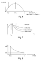
- Fig. 6 illustrates a diagram of output power versus the phase shift of the secondary stage of a converter with respect to its primary stage, according to some embodiments of the present invention
- Fig. 7 illustrates a diagram of output power (Gain) versus the frequency and load.
- Fig. 8 illustrates a diagram of efficiency versus the phase according to some embodiments of the invention.
- the invention described herein after pertains to an electrically isolated DC-DC converter that may be used to deliver power of DC voltage or AC voltage (high frequency of up to, for example, 1MHz yet the operational frequency high range may get higher as the technology of production of switching transistors improves) from a DC source such as a battery or rectifier utility.
- a transformer may be used to provide electrical isolation and a step-down or step-up in voltage level, according to its ratio, as may be required.
- Switching means such as transistors, preferably MOSFET
- diodes preferably of the fast recovery type may be used in conjunction with capacitors and inductors to induce non-DC current (i.e. AC or pulsating current) in the primary circuit to activate a transformer to create the required conversion.
- a control circuit may typically be included to provide the required driving signals to the transistor control terminals. The ability to provide a desired regulation performance is usually derived from the power circuit's topology and the manner in which its switching devices are controlled.
- FIGs. 1A and 1B are schematic diagrams of four-way converter 2 and two-way converter 4 respectively according to some embodiments of the present invention.
- Fig. 1A depicts converter 2 with a two-stage structure coupled by a transformer TR, where the power flows through the first stage (primary stage) and then through the second stage (secondary stage). Both stages may be provided with regulation units. Additionally, the secondary stage may be electrically isolated from the primary stage by transformer TR which may also provide a step-down or step-up function of DC and AC output voltages.
- both primary and secondary stages of converter 2 may comprise quad switching topology with switching means Q1a - Q1d and Q2a - Q2d in the first and second stages respectively.
- Switching means Q1a - Q1d and Q2a - Q2d may be realized by any suitable controllable switch that will stand the switching conditions developing during the operation of converter 2, such as switching frequency, switching current and switching voltage.
- Switching means Q1a - Q1d and Q2a - Q2d may be controlled by a control unit (not shown). The purpose of the control unit may be to determine when each of the switching means will be turned ON or OFF, in each stage respectively.
- Fig. 1B depicts converter 4 with a two-stage structure coupled by a transformer TR, where the power flows through the first stage (primary stage) and then through the second stage (secondary stage). Similarly to converter 2 of Fig.
- the secondary stage may be electrically isolated from the primary stage by transformer TR which may also provide a step-down or step-up function of DC and AC output voltages.
- Both primary and secondary stages of converter 4 may comprise dual switching topology with switching means Q10a - Q10b and Q20a - Q20b respectively. It would be apparent to one skilled in the art that any other topology of switching means, such as a full bridge (four-way) switching assembly in the primary stage and a half bridge (two-way) switching assembly in the secondary stage, or the like may be used.
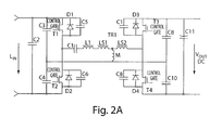
- FIG. 2A is a schematic illustration of a two stage DC-DC converter 6 according to some embodiments of the invention.
- Fig. 2A illustrates an embodiment implementing two power stages.
- each of the two stages comprises a half-bridge converter, yet it would be appreciated by a person of ordinary skill in the art that a full-bridge converter may similarly be used.
- Primary stage may comprise switching transistors T1, T2; fast-recovery diodes D1, D2; filtering capacitor C2; auxiliary capacitors C3, C4 and parasitic or implemented capacitors C5, C6.
- the secondary stage may substantially be a mirror picture of the primary stage: switching transistor T3, T4, diodes D3 and D4, parasitic or implemented capacitors C7 and C8; auxiliary capacitors C9, C10 and filtering capacitor C11.
- the two stages may be coupled through transformer TR1 which may comprise magnetizing inductance represented by inductor M and leakage inductances represented by inductors Ls1, Ls2; resonant inductance L1 and resonant capacitor C1.
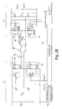
- Converter 20 may comprise two stages 21, 23 coupled by coupling means such as a transformer 30, resonant circuitry which may comprise resonant capacitor C1 and resonant inductor L1 and a controller 36.
- Input stage 21 may comprise input terminals for receiving input power having voltage Vin , filtering capacitor C2, auxiliary capacitors C3, C4 and switching assemblies 22 and 24, each may comprise switching means, fast recovery diode and parasitic / implemented capacitance.
- Output stage 23 may comprise switching assemblies 26, 28 each of which may comprise switching means, fast recovery diode and parasitic / implemented capacitance, auxiliary capacitors C9 and C10 and filtering capacitor C11.
- the output voltage Vout develops on output terminals of secondary stage 23.
- Primary stage 21 and secondary stage 23 may be coupled by a coupling transformer 30 which may comprise magnetizing inductance represented by inductor M and leakage inductances represented by inductors Ls1, Ls2; resonant inductance 32 and resonant capacitor 34.
- Switching assemblies 22, 24, 26 and 28 may be controlled by controller 36 which may be adapted to provide control signals to the control terminals of switching assemblies 22, 24, 26 and 28 according to any desired switching scheme. Controller 36 may further receive V REF AC representing actual voltage on the input terminals of converter 20; V REF DC to provide reference for the desired DC voltage and V FB OUT to provide feedback for the operation of converter 20 by providing voltage from the output terminals of converter 20.
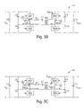
- Figs. 3A - 3F are partial schematic illustrations of a converter 10 according to embodiments of the present invention with indications of the current flow in branches of the converter in various steps of the working cycle. Attention is also made to Fig. 3A1 which depicts in more details optional topology and components comprised in switching assembly 11.
- Switching assembly 11 may be regarded as a generic topology of a switching means SWx (where x may have the values 1, 2, 3, or 4).
- Generic switching assembly 11 may comprise of transistor Tswx connected in parallel to diode Dsw x and to capacitor Csw x .
- switching assembly SWx may be any other appropriate device and circuitry.
- the control terminal denoted VgSWx is the control terminal through which switching assembly SWx may be turned (or gated) ON or OFF by a control circuitry 36 ( Fig. 2B ).
- Figs. 3A-3F are shown without a control unit, such as controller 36 of Fig.
- a control unit such as controller 36
- controller 36 may be used to control the operation of converter 10 by means of gating its switching devices SW1 - SW4 ON or OFF at the desired timing, as will be described in more details below.
- the description relating to Figs. 3A-3F intends mainly to describe the flow of currents in the branches of a converter in various phases of a work cycle, according to embodiments of the invention.
- the description of the flow of currents in a converter according to embodiments of the present invention is followed by a description of time graphs of voltages and currents in a converter according to the invention and respective control signals at the control gates of the switching devices.
- converter 10 may comprise a first stage comprising capacitors C2, C3 and C4 and switching means SW1 and Sw2, all connected between two poles of Vin, denoted Vin+ and Vin- respectively.
- Switching means SW1 and Sw2 may be connected in a totem-pole arrangement with a central tap denoted "1".
- converter 10 may comprise a second stage comprising switching means SW3 and SW4 and capacitors C9, C10 and C11, all connected between two poles of Vout, denoted Vout+ and Vout- respectively.
- Switching means SW3 and SW4 may be connected in a totem-pole arrangement with a central tap denoted "2".
- Further converter 10 may comprise a resonance circuit comprising inductor L1 and capacitor C1 connected between said first central tap "1" and said second central tap “2", either directly (not shown in Fig. 3A but exemplified in other drawings) or via a coupling transformer TR1. Additionally converter 10 may comprise a return path between said first and said second stages connected between point "3", being a third central tap between capacitor C3 and capacitor C4 and point "4" being a fourth central tap between capacitor C9 and capacitor C10. the return path of resonance circuit may be connected directly between points "3" and "4" (not shown in Fig. 3A but exemplified in other drawings) or via a coupling transformer TR1.
- node of capacitors C3 and C4, as well as the node of C9 and C10 may be replaced by an additional arrangement of two switching means arranged in totem-pole arrangement with their central tap at point "3" or "4" respectively, such as in a converter occupying a full-bridge at each stage.
- switching assemblies SW1 and SW3 are conducting (that is are switched ON), switching assemblies SW2 and SW4 are gated OFF; capacitor CSW1 of switching assembly SW1 is charged to 0 volts, capacitor Csw2 of switching assembly SW2 is charged to Vin, capacitor Csw3 of switching assembly SW3 is charged to 0 volts, and capacitor C10 to Vout.
- Resonant inductor L1 and leakage inductances Ls1, Ls2,magnetized by currents Isw 1,2 and Isw 3 , 4 are flowing from Vin to Vout (the description of currents Isw 1,2 and Isw 3,4 as flowing 'through' transformer TR1 is a common way of describing a simplified transformer coupled circuitry, specifically if the transformation ratio is 1: 1).
- Fig. 3B shows the next step in the sequence of four steps of the presently described embodiment.
- current ISW1,2 begins to charge capacitors CSW1 and CSW2. Because the initial voltage on capacitor CSW1 is substantially zero, the mode of the switching is substantially ZVS, because the switching of switching assembly SW1 is done when the voltage across its terminals is substantially zero. Because the shape of the current ISW1,2 is sine, and the value of the current is minimum (efficient for recharge of capacitors CSW1, CSW2), the implemented mode might be named ZVS.
- the recharge of the respective capacitors CSW1 and Csw2 forms the roll-off of voltage in point 1 (see Fig 3A ).
- the voltage at point 1 in Fig. 3A
- the current through the diode turns diode DSW2 ON.
- the transition time of change of voltage across SW1 is the time between t 2 and t 3 (see Figs 4A-5D ). Only after that, at time t 4 , control signal V GSW2 is applied to SW2 to turn the switching assembly ON.
- the currents are described in Fig. 3B . At this time the changes in voltage has finished
- Fig. 3C shows a next step in the sequence of operation of converter 10 according some embodiments of the invention.
- current ISW1,2 changed its direction in the current loop of the first stage of converter 10 (see t 5 , Fig. 4A )
- the direction of current ISW3,4 in the current loop of the second stage is also changed (see t 5 , Fig. 4C ).
- control signal VGSW3 is applied to switching assembly SW3 and by that it will turn the switching means OFF and current ISW3,4 will start recharging capacitors CSW3, CSW4. See t 6 in Fig. 5C . Because the initial voltage on capacitor CSW3 is now substantially zero, the switching mode is substantially purely ZVS.
- the implemented mode is substantially ZCS.
- the recharge of the respective capacitors C sw3 and C sw4 is forming the roll-off of voltage in point 2.
- the corresponding time points are t 6 and t 7 respectively.
- the end of the recharge cycle turns diode D4 ON. Only after that, at time t 8 , control signal VGSW4 is applied to transistor SW4 to turn it ON.
- the time of this recharge cycle, t 6 -t 7 is a transition time.
- the currents of this step are as depicted in Fig. 3D . By the end of this time the change in all voltages in this cycle fraction has finished.
- a signal that is applied to V GSW2 turns assembly SW2 now to OFF (at t 9 ).
- Current ISW1,2 begins to recharge capacitors CSW1, CSW2. Because initial voltage of capacitor CSW2 is substantially zero, and the current ISW1,2 charges C SW1 and C SW2 according to the slope of V SW1-2 between t 9 to t 10 .
- the implemented mode of this switching is substantially ZVS. Because the shape of the current as function of time is substantially a sine and is approaching crossing zero but not exactly zero - which is important to support charging of the capacitors, the mode of switching is substantially ZCS.
- the recharge process forms the roll-off of voltage in point 1, as shown in Fig. 3E .
- diode DSW1 When diode DSW1 is turned ON it indicates the end of the recharge stage of C SW1 . Only after that signal VGSW1 is applied to switching assembly SW1 to turn it ON. The time of this recharge is a transition time lasting between t 9 to t 10 . By the end of this time the voltage changing in point 1 has finished.
- the direction of currents I SW1,2 and I SW3,4 alternates respectively as indicated in Fig. 3F .
- Switching off transistor SW4 at time t13, initiates recharge process of capacitors CSW3, CSW4 .
- SW4 is switched off and in accordance with the direction of current ISW3,4, recharges Csw3 and Csw4 until Vsw 3-4 reaches, during transition time, maximum voltage between t13 to t14.
- the switching conditions are ZVS and ZCS, similarly to the previous stages. Substantially with the conditions satisfying ZVC and ZCS at SW4.
- the recharge time of the capacitors is a transition time and it finishes when diode DSW3 is turned ON (see t 14 , Figs 4A - 5D ). After it, by means of control signal VGSW3 switching assembly SW3 is turned ON, at time t15. at the end of this stage the circuit is ready to arrive at the initial state, as described above, at the end of the cycle.
- Fig. 3G is a simplified equivalent scheme 300 of a converter according to embodiments of the present invention.
- Equivalent scheme 300 may faithfully represent a two-stage converter according to the present invention under several reasonable assumptions.
- the leakage inductance (which is represented in Figs.2A and 2B , for example, by LS1 and LS2) is equal substantially to zero. Therefore the coils representing the leakage inductances may be removed in this scheme.
- the transfer ratio of the transformer is 1:1 then the voltage at the terminals of the primary stage of the transformer is equal to that on the terminals of the secondary stage and same applies to currents in the primary and secondary windings. Therefore the transformer may be removed completely from equivalent scheme 300.
- input stage 302 may be connected, under these assumptions to output stage 304 directly by Li-C1 resonant tank.
- input stage 302 may comprise a set of switching assemblies SW1, SW2 and output stage 304 may comprise a set of switching assemblies SW3, SW4.
- SW1-SW4 may be controlled (i.e. gated) ON or OFF via their respective control terminals Vgsw1 - Vgsw4 respectively by applying control signals from, for example, controller 36.
- Equivalent scheme 300 may be used for simplified analysis of the operation of a converter operating in accordance with embodiments of the present invention. Based on equivalent scheme 300 it will be apparent that the currents in the input stage 302 and in the output stage 304 are the same.
- Figs. 4A-4D and 5A-5D are wave forms in the time-domain of current through and voltage across switching devices at both sides of a converter and simplified illustrations of switching timing diagrams of control signals at the gate terminals of switching devices of a converter, according to some embodiments of the present invention.
- transistors SW1 and SW3 are conducting (that is are switched ON)
- transistors SW2 and SW4 are gated OFF.
- Capacitor CSW1 of transistor SW1 is then charged to 0 volts, and capacitor Csw2 to Vin.
- Capacitor Csw3 is charged to 0 volts, and capacitor Csw4 to Vout.
- Resonant inductor L1 and leakage inductances Ls1, Ls2 are then magnetized by currents Isw1-2 and Isw3-4 which are flowing from Vin terminals to Vout terminals and then back from Vout terminals to Vin terminals.
- the switching scheme described above begins at time t 2 in Figs. 4A-4D and 5A-5D .
- Figs. 4B and 4D present the voltages V SW1 , 2 at point 1 and V SW3,4 at point 2.
- the switching timing schemes of V GSW1 - V GSW4 are presented in Figs. 5A to 5D .
- the switching is done in roll-off mode signals and not in roll-on mode signals.
- the switching schemes of Figs. 5A to 5D present the switching ON or OFF of V GSW1 - V GSW4 in each step of the various steps described above with respect to Figs. 3A - 3F .
- the amplitudes of the resonant tank comprising inductance L1 and capacitance C1, currents ISW1,2,3,4 and the value of output voltage Vout may vary according to the variation of frequency/time of the cycle period. This is one of the embodiments for regulation of the values of the currents ISW1,2,3,4 and the voltage Vout.
- graphs of Figs. 4A - 5D reflect the values related to the chosen phase difference between the voltages of the input (primary) stage, i.e. VSW1,2 and the output (secondary) stage, i.e., VSW3,4.
- the time between t 2 to t 6 . is the phase shift ⁇ .
- the phase is ⁇ /T.
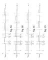
- Figs. 6, 7 and 8 are a diagram of output power versus the phase of the secondary stage of a converter with respect to its primary; a diagram of output power (Gain) versus the frequency and load and a diagram of efficiency versus the phase according to some embodiments of the invention.
- the variation of the phase may impose variations of the output voltage Vout, of the output power Pout and the currents ISW1,2 and ISW3,4.
- the dynamic range of change of phase from zero to ⁇ may be divided to three main sub-regions, denoted I, II and III in Fig. 6 .
- the operational frequency range for a converter of the present invention may also be divided to three sub-regions.
- First frequency sub-region, denoted I in Fig. 7 extends substantially from f 0 to f min , where f 0 is the natural resonance frequency of the resonant tank of a converter according to the present invention and f min is the frequency at which for a given load of the converter the phase is approx. 0.2 ⁇ when control signals of the primary and secondary stages of the converter are in-phase of the resonant tank and the reactive current is just large enough to enable soft switching.
- Second frequency sub-region, denoted II extends substantially from f min , to f 1 where f 1 is the frequency at which for a given load of the converter the phase is approx.
- a third frequency sub-region extends substantially from f 1 to f 2 where f 2 is the maximum available frequency at which soft switching is still possible for a given converter circuitry. This frequency highly depends on the switching rate of the switching assemblies of the converter.
- the control of the phase in a converter of the present invention when in sub-region II is achieved by means of change of the frequency of the converter which imposes change of the phase as a result of the change of the reaction of the secondary stage of the converter to the operation of the resonant tank.
- the control of the phase is achieved by means of change of the phase directly by means of control of the switching ON or OFF of the switching assemblies of the secondary stage of the converter relative to the switching of the primary stage of the converter.
- the controller may issue control signals so as to keep the value of phase at substantially 0.2 ⁇ and regulate Pout and Vout only by means of changing the frequency.
- the goal of this process is to operate the converter, as much as possible, in one-sided regulation mode and achieve high efficiency.
- a second range of phase values where the frequency equals f 1 and higher, when the phase between the voltage and current of the resonant tank exceeds 0.5 ⁇ the system of the present invention performs the variation of phase by means of the control signals.
- the regulation is one-sided, which enables to regulate the output of the converter either by control of the phase or by control of the frequency or by both.
- the latter is better because simultaneous regulation (i.e. by control of both the phase and the frequency) may increase the efficiency when at low or non load and at high input voltage, or when output voltage is very low.
- Control scheme of a converter built and operating according to embodiments of the present invention may be presented with respect a two-dimensional space of working conditions of the converter, having the phase angle as one axis and the frequency as its other axis.
- two-dimensional space is partitioned into nine regions, which may be denoted, for example, region f I -p II , which defines the region where the frequency of the converter is in its I sub-region and the phase is in its II sub-region.
- Control of the frequency may be achieved by changing the switching rate of all four switching assemblies 22, 24, 26 and 28 substantially in the same extent.
- Control of the phase of the converter of the present invention may be achieved by changing the switching timing scheme of switching assemblies 26 and 28 of the secondary stage of the converter 20 with respect to the timing of switching assemblies 22 and 24 of the primary stage of the converter. As much as the switching scheme of the secondary stage is delayed with respect to that of the primary stage the phase angle grows.
- a converter built and operating according to the present invention to convert AC input voltage into the desired value of DC output voltage.
- Additional advantage feature of the converter is to use available DC power at the output terminals and convert it into AC power at, for example, a AC high frequency output terminals, as shown in Fig. 1A .
- the second stage may derive power from a output capacitor (for example C11 in Fig. 2 ) to provide AC voltage to the AC output 5 in converter 4 of Fig. 1B .
- the input is supplied with AC voltage at low frequency of, for example, 50 Hz, and the output voltage AC at high frequency of up to, for example, 1MHz.
- the efficiency of this embodiment may go up to 97%.
Abstract
A DC-DC converter apparatus comprising half or full bridge, two-stage resonant converter, which may include series resonant (inductor, capacitor) devices. An isolated transformer having primary and secondary winding supplies current to full-wave secondary stage-bridge through the use of primary winding resonant devices employing primary stage-bridge. The magnetizing of said devices employs zero-current, zero-voltage resonant-transition switching technology, which reduces switching losses at all switching frequencies to almost zero. The regulation of output voltage at all loads and input voltages achieved by the control of the switching frequency and the phase between signals for primary and secondary stages. The proper intermittent of the frequency and the phase allows achieving the value of efficiency up to 97%.
Description
- This invention relates generally to a switching power converter and, more specifically, to a two-stage converter with transformer separation having improved zero voltage switching (ZVS) and zero current switching (ZCS) operation modes.
- The increased demand in the field of power conversion-size reduction and high-efficiency is difficult to meet with the present available power converters. Some features inherent in devices of relevant technology militate against achievement of the desired goals. Some converters are specifically designed to handle a wide range of output loads and variations of input voltage, resulting in less efficiency. Reducing the size of components (capacitors and magnetic component) related to high switching frequency and as results to concomitant high switching losses.
- Common approach of ZVS and ZCS topology disclosed in the prior art is series resonant converter described in e.g. USOORE33866E,
US6.178.099B1 that achieves nearly lossless soft switching using pulse width modulation and frequency super-resonant control of commutation in full or half bridge converter. Soft switching converters attempt to take advantage of the parasitic effect of components within the converter in order to reduce the voltage potentials across (and current flows through) the switches before effecting a switching operation. More specifically, soft switching converters adjust the switching timing in order to charge and to discharge the parasitic switch capacitances of the transistors through the use of current supplied by the magnetizing inductance of the winding of the transformer, thereby reducing the voltage across Off or Open transistors, and current flow through On or Closed transistors. During the time switching which transistors takes, the soft switching reduces the power losses during the switching operation, thereby enabling the converter to operate at high frequency, high efficiency and with reduced electromagnetic interference. - However, the operation with typical pulse width modulation or the variation of switching frequency is a deficient in full volume of line and maximal load alternation which leads to stresses on the switching devices which are similar to those of a hard switched converter.
- At the series resonant converters disclosed in, e.g.,
US4855.888 andEP 0503862B1 there is presented the topology of two-stage (full or half bridge) circuitry connected to input voltage. In the similar devices, such as those disclosed inUS 5,999,417 orUS 6,930,893 two stages are floating relatively to one another, where the output voltages are algebraic sum voltages of the output voltages of the two stages. The regulation of the output voltages is achieved by alteration of the phase between the the two stages of the converter. However, the operation in full volume (from 0 to max) of loads and line variation leads to inevitable hard switching, e.g., excessive switching losses, excessive EMI and the like. - Quasi-resonant bidirectional converters were introduced in
US4.663.699 and Natural ZVS Medium-Power Bidirectional DC-DC Converters with Minimum Numbers of Devices, Hui Li Fang Zheng Peng, J.S. Lawlee, IEEE, Vol. 39, No. 2, March/April 2003. Presented two stage active half-bridge topology featured ZVS in full volume of line and load variation. However, high current switching leads to high level conductive and switching losses, and causes the limitation to power, obstacles to decrease the cost, volume and EMI. - From this prior art other challenge is presented to minimize losses during the switch transition time of two stage active full bridge or half-bridge converter.
- The present invention comprises two stages active full or half bridge switching circuits. The circuits comprise of four or two switches, respectively. Two stage connected by transformers where primary winding through series resonant tank applied to first stage, secondary winding to second stage. First stage is supplied by input voltages, second derives output voltage, DC or AC. The stages may be controlled by signals produced by a controller. The simultaneous changing of frequency and phase between signals attributed to first and second stage may feature the variation of output voltage from 0 to max at full alternation of line (input voltages, for example, rectified 50Hz "Voltage Main") voltages and loads.
- The present invention, in embodiments described hereinafter, may offer one, some, or all of the following advantages and features:
- 1. ZVS, ZCS in every combination of input voltages, output voltages and load from light (no-load) to max.
- 2. Load switching losses related to ZVS, ZCS.
- 3. Low conductive losses due to minimized value and sine shape of the current conducted through resonant tank and switching stages.
- 4. High efficiency due to low switching and conductive losses.
- 5. Means to distribute DC and AC voltage which are fully adjusted to the value of DC output voltages and to feature efficiency of up to 97%.
- For a more complete understanding of the present invention and its advantages, the description of the invention should be read in conjunction with the following drawings in which:
-
Figs. 1A and 1B are schematic diagrams of four-way and two-way converter according to some embodiments of the present invention; -
Fig. 2A is a schematic illustration of a two stage embodiment of a converter according to some embodiments ofFig. 1 ;Fig. 2B is a schematic illustration of a converter with control unit according to some embodiments of the present invention -
Figs. 3A - 3F , are illustrations of a converter according to the present invention and indications of current flow in branches of the converter in various steps of the working cycle;Fig. 3G is simplified equivalent scheme of a converter according to embodiments of the present invention; -
Figs. 4A - 4D are simplified illustrations of wave forms in the time-domain of current through and voltage across switching devices at both sides of a converter according to some embodiments of the present invention; -
Figs. 5A - 5D are simplified illustrations of switching timing diagrams of control signals at the gate terminals of switching devices of a converter according to some embodiments of the present invention; -
Fig. 6 illustrates a diagram of output power versus the phase shift of the secondary stage of a converter with respect to its primary stage, according to some embodiments of the present invention; -
Fig. 7 illustrates a diagram of output power (Gain) versus the frequency and load; and -
Fig. 8 illustrates a diagram of efficiency versus the phase according to some embodiments of the invention. - It will be appreciated that for simplicity and clarity of illustration, elements shown in the figures have not necessarily been drawn to scale. For example, the dimensions of some of the elements may be exaggerated relative to other elements for clarity. Further, where considered appropriate, reference numerals may be repeated among the figures to indicate corresponding or analogous elements.
- The invention described herein after pertains to an electrically isolated DC-DC converter that may be used to deliver power of DC voltage or AC voltage (high frequency of up to, for example, 1MHz yet the operational frequency high range may get higher as the technology of production of switching transistors improves) from a DC source such as a battery or rectifier utility. In such a converter, a transformer may be used to provide electrical isolation and a step-down or step-up in voltage level, according to its ratio, as may be required. Switching means (such as transistors, preferably MOSFET) and diodes, preferably of the fast recovery type may be used in conjunction with capacitors and inductors to induce non-DC current (i.e. AC or pulsating current) in the primary circuit to activate a transformer to create the required conversion. A control circuit may typically be included to provide the required driving signals to the transistor control terminals. The ability to provide a desired regulation performance is usually derived from the power circuit's topology and the manner in which its switching devices are controlled.
- Attention is made now to
Figs. 1A and 1B which are schematic diagrams of four-way converter 2 and two-way converter 4 respectively according to some embodiments of the present invention.Fig. 1A depictsconverter 2 with a two-stage structure coupled by a transformer TR, where the power flows through the first stage (primary stage) and then through the second stage (secondary stage). Both stages may be provided with regulation units. Additionally, the secondary stage may be electrically isolated from the primary stage by transformer TR which may also provide a step-down or step-up function of DC and AC output voltages. Inconverter 2 both primary and secondary stages ofconverter 2 may comprise quad switching topology with switching means Q1a - Q1d and Q2a - Q2d in the first and second stages respectively. Switching means Q1a - Q1d and Q2a - Q2d may be realized by any suitable controllable switch that will stand the switching conditions developing during the operation ofconverter 2, such as switching frequency, switching current and switching voltage. Switching means Q1a - Q1d and Q2a - Q2d may be controlled by a control unit (not shown). The purpose of the control unit may be to determine when each of the switching means will be turned ON or OFF, in each stage respectively.Fig. 1B depictsconverter 4 with a two-stage structure coupled by a transformer TR, where the power flows through the first stage (primary stage) and then through the second stage (secondary stage). Similarly toconverter 2 ofFig. 1A , the secondary stage may be electrically isolated from the primary stage by transformer TR which may also provide a step-down or step-up function of DC and AC output voltages. Both primary and secondary stages ofconverter 4 may comprise dual switching topology with switching means Q10a - Q10b and Q20a - Q20b respectively. It would be apparent to one skilled in the art that any other topology of switching means, such as a full bridge (four-way) switching assembly in the primary stage and a half bridge (two-way) switching assembly in the secondary stage, or the like may be used. - Attention is made now to
Fig. 2A which is a schematic illustration of a two stage DC-DC converter 6 according to some embodiments of the invention.Fig. 2A illustrates an embodiment implementing two power stages. In this circuit, each of the two stages comprises a half-bridge converter, yet it would be appreciated by a person of ordinary skill in the art that a full-bridge converter may similarly be used. Primary stage may comprise switching transistors T1, T2; fast-recovery diodes D1, D2; filtering capacitor C2; auxiliary capacitors C3, C4 and parasitic or implemented capacitors C5, C6. The secondary stage may substantially be a mirror picture of the primary stage: switching transistor T3, T4, diodes D3 and D4, parasitic or implemented capacitors C7 and C8; auxiliary capacitors C9, C10 and filtering capacitor C11. The two stages may be coupled through transformer TR1 which may comprise magnetizing inductance represented by inductor M and leakage inductances represented by inductors Ls1, Ls2; resonant inductance L1 and resonant capacitor C1. - Attention is made now further to
Fig. 2B , which is a schematic illustration of a converter 20 according to some embodiments of the present invention. Converter 20 may comprise twostages transformer 30, resonant circuitry which may comprise resonant capacitor C1 and resonant inductor L1 and acontroller 36.Input stage 21 may comprise input terminals for receiving input power having voltage Vin , filtering capacitor C2, auxiliary capacitors C3, C4 and switchingassemblies 22 and 24, each may comprise switching means, fast recovery diode and parasitic / implemented capacitance.Output stage 23 may comprise switchingassemblies secondary stage 23.Primary stage 21 andsecondary stage 23 may be coupled by acoupling transformer 30 which may comprise magnetizing inductance represented by inductor M and leakage inductances represented by inductors Ls1, Ls2;resonant inductance 32 andresonant capacitor 34.Switching assemblies controller 36 which may be adapted to provide control signals to the control terminals of switchingassemblies Controller 36 may further receive VREF AC representing actual voltage on the input terminals of converter 20; VREF DC to provide reference for the desired DC voltage and VFB OUT to provide feedback for the operation of converter 20 by providing voltage from the output terminals of converter 20. - Attention is made now to
Figs. 3A - 3F which are partial schematic illustrations of aconverter 10 according to embodiments of the present invention with indications of the current flow in branches of the converter in various steps of the working cycle. Attention is also made toFig. 3A1 which depicts in more details optional topology and components comprised in switchingassembly 11.Switching assembly 11 may be regarded as a generic topology of a switching means SWx (where x may have thevalues Generic switching assembly 11 may comprise of transistor Tswx connected in parallel to diode Dswx and to capacitor Cswx. In the circuits discussed herein below, a switching means will be referred to as a switching assembly of the generic type discussed above, yet it would be apparent to a person skilled in the art that switching assembly SWx may be any other appropriate device and circuitry. The control terminal denoted VgSWx is the control terminal through which switching assembly SWx may be turned (or gated) ON or OFF by a control circuitry 36 (Fig. 2B ).Figs. 3A-3F are shown without a control unit, such ascontroller 36 ofFig. 2B , for more clarity yet it should be apparent to a person with ordinary skill in the art that a control unit, such ascontroller 36, may be used to control the operation ofconverter 10 by means of gating its switching devices SW1 - SW4 ON or OFF at the desired timing, as will be described in more details below. The description relating toFigs. 3A-3F intends mainly to describe the flow of currents in the branches of a converter in various phases of a work cycle, according to embodiments of the invention. The description of the flow of currents in a converter according to embodiments of the present invention is followed by a description of time graphs of voltages and currents in a converter according to the invention and respective control signals at the control gates of the switching devices. - As depicted in
Fig. 3A (and may be applicable to converters presented in other drawings as well, with the required changes)converter 10 may comprise a first stage comprising capacitors C2, C3 and C4 and switching means SW1 and Sw2, all connected between two poles of Vin, denoted Vin+ and Vin- respectively. Switching means SW1 and Sw2 may be connected in a totem-pole arrangement with a central tap denoted "1". Similarly,converter 10 may comprise a second stage comprising switching means SW3 and SW4 and capacitors C9, C10 and C11, all connected between two poles of Vout, denoted Vout+ and Vout- respectively. Switching means SW3 and SW4 may be connected in a totem-pole arrangement with a central tap denoted "2".Further converter 10 may comprise a resonance circuit comprising inductor L1 and capacitor C1 connected between said first central tap "1" and said second central tap "2", either directly (not shown inFig. 3A but exemplified in other drawings) or via a coupling transformer TR1. Additionallyconverter 10 may comprise a return path between said first and said second stages connected between point "3", being a third central tap between capacitor C3 and capacitor C4 and point "4" being a fourth central tap between capacitor C9 and capacitor C10. the return path of resonance circuit may be connected directly between points "3" and "4" (not shown inFig. 3A but exemplified in other drawings) or via a coupling transformer TR1. It will be noted that in other embodiments of the present invention the node of capacitors C3 and C4, as well as the node of C9 and C10 may be replaced by an additional arrangement of two switching means arranged in totem-pole arrangement with their central tap at point "3" or "4" respectively, such as in a converter occupying a full-bridge at each stage. - When switching assemblies SW1 and SW3 are conducting (that is are switched ON), switching assemblies SW2 and SW4 are gated OFF; capacitor CSW1 of switching assembly SW1 is charged to 0 volts, capacitor Csw2 of switching assembly SW2 is charged to Vin, capacitor Csw3 of switching assembly SW3 is charged to 0 volts, and capacitor C10 to Vout. Resonant inductor L1 and leakage inductances Ls1, Ls2,magnetized by currents Isw1,2 and Isw3,4 are flowing from Vin to Vout (the description of currents Isw1,2 and Isw3,4 as flowing 'through' transformer TR1 is a common way of describing a simplified transformer coupled circuitry, specifically if the transformation ratio is 1: 1).
-
Fig. 3B shows the next step in the sequence of four steps of the presently described embodiment. After the switching assembly SW1 is gated OFF by control signal VGSW1, current ISW1,2 begins to charge capacitors CSW1 and CSW2. Because the initial voltage on capacitor CSW1 is substantially zero, the mode of the switching is substantially ZVS, because the switching of switching assembly SW1 is done when the voltage across its terminals is substantially zero. Because the shape of the current ISW1,2 is sine, and the value of the current is minimum (efficient for recharge of capacitors CSW1, CSW2), the implemented mode might be named ZVS. - The recharge of the respective capacitors CSW1 and Csw2 forms the roll-off of voltage in point 1 (see
Fig 3A ). At the end of that recharge step the voltage at point 1 (inFig. 3A ), and in accordance also the current through the diode turns diode DSW2 ON. The transition time of change of voltage across SW1 is the time between t2 and t3 (seeFigs 4A-5D ). Only after that, at time t4 , control signal VGSW2 is applied to SW2 to turn the switching assembly ON. The currents are described inFig. 3B . At this time the changes in voltage has finished -
Fig. 3C shows a next step in the sequence of operation ofconverter 10 according some embodiments of the invention. After current ISW1,2 changed its direction in the current loop of the first stage of converter 10 (see t5,Fig. 4A ) the direction of current ISW3,4 in the current loop of the second stage is also changed (see t5,Fig. 4C ). Only after that control signal VGSW3 is applied to switching assembly SW3 and by that it will turn the switching means OFF and current ISW3,4 will start recharging capacitors CSW3, CSW4. See t6 inFig. 5C . Because the initial voltage on capacitor CSW3 is now substantially zero, the switching mode is substantially purely ZVS. Because the value of current ISW3,4 is minimum (enough for efficient recharging of capacitors CSW3, CSW4), the implemented mode is substantially ZCS. The recharge of the respective capacitors Csw3 and Csw4 is forming the roll-off of voltage inpoint 2. The corresponding time points are t6 and t7 respectively. The end of the recharge cycle turns diode D4 ON. Only after that, at time t8 , control signal VGSW4 is applied to transistor SW4 to turn it ON. The time of this recharge cycle, t6-t7, is a transition time. The currents of this step are as depicted inFig. 3D . By the end of this time the change in all voltages in this cycle fraction has finished. A signal that is applied to VGSW2 turns assembly SW2 now to OFF (at t9 ). Current ISW1,2 begins to recharge capacitors CSW1, CSW2. Because initial voltage of capacitor CSW2 is substantially zero, and the current ISW1,2 charges CSW1 and CSW2 according to the slope of VSW1-2 between t9 to t10 . The implemented mode of this switching is substantially ZVS. Because the shape of the current as function of time is substantially a sine and is approaching crossing zero but not exactly zero - which is important to support charging of the capacitors, the mode of switching is substantially ZCS. - The recharge process forms the roll-off of voltage in
point 1, as shown inFig. 3E . When diode DSW1 is turned ON it indicates the end of the recharge stage of CSW1. Only after that signal VGSW1 is applied to switching assembly SW1 to turn it ON. The time of this recharge is a transition time lasting between t9 to t10. By the end of this time the voltage changing inpoint 1 has finished. In accordance with the change of direction of the voltage applied to inductance L1 the direction of currents ISW1,2 and ISW3,4 alternates respectively as indicated inFig. 3F . Switching off transistor SW4, at time t13, initiates recharge process of capacitors CSW3, CSW4 . - At time t13 SW4 is switched off and in accordance with the direction of current ISW3,4, recharges Csw3 and Csw4 until Vsw 3-4 reaches, during transition time, maximum voltage between t13 to t14. The switching conditions are ZVS and ZCS, similarly to the previous stages. Substantially with the conditions satisfying ZVC and ZCS at SW4. The recharge time of the capacitors is a transition time and it finishes when diode DSW3 is turned ON (see t14 ,
Figs 4A - 5D ). After it, by means of control signal VGSW3 switching assembly SW3 is turned ON, at time t15. at the end of this stage the circuit is ready to arrive at the initial state, as described above, at the end of the cycle. - As may be clearly seen above, all changes in the direction of currents ISW1,2, ISW3,4 are followed by the value and the polarity of voltages applied to inductor L1 and whole resonant tank-L1 and C1. All the transition times relate to the values of ISW1,2, ISW3,4 and values of capacitors CSW1, CSW2, CSW3, CSW4 that include the parasitic capacitors of the transistors, and optionally also the auxiliary capacitors.
- Attention is made now to
Fig. 3G , which is asimplified equivalent scheme 300 of a converter according to embodiments of the present invention.Equivalent scheme 300 may faithfully represent a two-stage converter according to the present invention under several reasonable assumptions. In an ideal transformer the leakage inductance (which is represented inFigs.2A and2B , for example, by LS1 and LS2) is equal substantially to zero. Therefore the coils representing the leakage inductances may be removed in this scheme. Assuming that the transfer ratio of the transformer is 1:1 then the voltage at the terminals of the primary stage of the transformer is equal to that on the terminals of the secondary stage and same applies to currents in the primary and secondary windings. Therefore the transformer may be removed completely fromequivalent scheme 300. Thus,input stage 302 may be connected, under these assumptions tooutput stage 304 directly by Li-C1 resonant tank. As seen inFig. 3G input stage 302 may comprise a set of switching assemblies SW1, SW2 andoutput stage 304 may comprise a set of switching assemblies SW3, SW4. SW1-SW4 may be controlled (i.e. gated) ON or OFF via their respective control terminals Vgsw1 - Vgsw4 respectively by applying control signals from, for example,controller 36.Equivalent scheme 300 may be used for simplified analysis of the operation of a converter operating in accordance with embodiments of the present invention. Based onequivalent scheme 300 it will be apparent that the currents in theinput stage 302 and in theoutput stage 304 are the same. - From
equivalent scheme 300 ofFig. 3G it is evident that the current of input stage 302 (or ISW1,2) which is presented inFig. 4A is equal to the current of the output stage 304 (or ISW3,4) which is presented inFig. 4C . - Attention is made now also to
Figs. 4A-4D and5A-5D which are wave forms in the time-domain of current through and voltage across switching devices at both sides of a converter and simplified illustrations of switching timing diagrams of control signals at the gate terminals of switching devices of a converter, according to some embodiments of the present invention. Substantially when transistors SW1 and SW3 are conducting (that is are switched ON), transistors SW2 and SW4 are gated OFF. Capacitor CSW1 of transistor SW1 is then charged to 0 volts, and capacitor Csw2 to Vin. Capacitor Csw3 is charged to 0 volts, and capacitor Csw4 to Vout. Resonant inductor L1 and leakage inductances Ls1, Ls2 are then magnetized by currents Isw1-2 and Isw3-4 which are flowing from Vin terminals to Vout terminals and then back from Vout terminals to Vin terminals. The switching scheme described above begins at time t2 inFigs. 4A-4D and5A-5D . -
Figs. 4B and4D present the voltages VSW1,2 atpoint 1 and VSW3,4 atpoint 2. The switching timing schemes of VGSW1 - VGSW4 are presented inFigs. 5A to 5D . The switching is done in roll-off mode signals and not in roll-on mode signals. With respect to the momentarily values of ISW1,2 and ISW3,4 (Figs. 4A and 4C respectively) the switching schemes ofFigs. 5A to 5D present the switching ON or OFF of VGSW1 - VGSW4 in each step of the various steps described above with respect toFigs. 3A - 3F . - t1 - switching assembly SW1 is turned ON (
Fig. 3B ). The transition time must be completed first. - t2 - switching assembly SW1 is gated OFF.
- t3 - switching assembly SW1 and SW2 is turned OFF. The transition time is t2 - t3 must be completed.
- t4 - switching assembly SW2 is gated ON.
- t5 - switching assembly SW2 is turned ON. The current Isw3-4 changes polarity.
- t6 - switching assembly SW3 is gated OFF.
- t7 - switching assembly SW3 is turned OFF.
- t8 - SW4 is turned ON.
- t9 - switching assembly SW2 is turned OFF
- t10 - switching assembly SW2 is turned ON
- As shown in
Fig. 4A to Fig. 5D , the amplitudes of the resonant tank comprising inductance L1 and capacitance C1, currents ISW1,2,3,4 and the value of output voltage Vout may vary according to the variation of frequency/time of the cycle period. This is one of the embodiments for regulation of the values of the currents ISW1,2,3,4 and the voltage Vout. It should be noted that graphs ofFigs. 4A - 5D reflect the values related to the chosen phase difference between the voltages of the input (primary) stage, i.e. VSW1,2 and the output (secondary) stage, i.e., VSW3,4. The time between t2 to t6.is the phase shift δ. Related to the period (T).the phase is δ/T. - Attention is made now to
Figs. 6, 7 and 8 , which are a diagram of output power versus the phase of the secondary stage of a converter with respect to its primary; a diagram of output power (Gain) versus the frequency and load and a diagram of efficiency versus the phase according to some embodiments of the invention. As shown inFig. 6 , the variation of the phase may impose variations of the output voltage Vout, of the output power Pout and the currents ISW1,2 and ISW3,4. The dynamic range of change of phase from zero to π may be divided to three main sub-regions, denoted I, II and III inFig. 6 . From a phase value of substantially zero to phase of approximately 0.2π (sub-region I) no control of Pout by means of phase shift changes is done. From phase value of 0.2π to 0.5π (sub-region II) the value of Pout and Vout increase to a maximum, and then, in sub-region III, decrease to substantially zero when the phase value reaches π. Sub-region I is practically not an operational range of control by phase change because only in phase values above 0.2π does soft-switching begins to be effective. Yet, the range of phase above 0.2π is preferable for exercising some embodiments of the invention. The cause is that higher efficiency is achieved at this range (from approximately 96% at 0.2π to approximately 90% at π), as shown inFig. 8 . Thus it would be clear that the regulation of a converter circuit according to the present invention by means of controlling the phase has to be featured substantially from phase value of 0.2π to π. This is another embodiment for regulation of the converter parameters. - The operational frequency range for a converter of the present invention may also be divided to three sub-regions. First frequency sub-region, denoted I in
Fig. 7 extends substantially from f0 to fmin, where f0 is the natural resonance frequency of the resonant tank of a converter according to the present invention and fmin is the frequency at which for a given load of the converter the phase is approx. 0.2π when control signals of the primary and secondary stages of the converter are in-phase of the resonant tank and the reactive current is just large enough to enable soft switching. Second frequency sub-region, denoted II, extends substantially from fmin, to f1 where f1 is the frequency at which for a given load of the converter the phase is approx. 0.5π when control signals of the primary and secondary stages of the converter are in-phase of the resonant tank. A third frequency sub-region, denoted III, extends substantially from f1 to f2 where f2 is the maximum available frequency at which soft switching is still possible for a given converter circuitry. This frequency highly depends on the switching rate of the switching assemblies of the converter. It should be noted that in a preferred embodiment the control of the phase in a converter of the present invention when in sub-region II is achieved by means of change of the frequency of the converter which imposes change of the phase as a result of the change of the reaction of the secondary stage of the converter to the operation of the resonant tank. When operating in phase sub-region III the control of the phase is achieved by means of change of the phase directly by means of control of the switching ON or OFF of the switching assemblies of the secondary stage of the converter relative to the switching of the primary stage of the converter. - When planning a control scheme for a converter according to the present invention it should be noted that working in sub-regions II and III of phase, that is from phase of 0,2π to 0.5π and from 0.5π to π respectively, imposes requirements on the regulation of a converter of the present invention that may be contradicting. A reason for that is that one-sided variation of the phase (i.e. - changing the phase of the secondary stage of a converter with respect to the primary stage) results two-sided variation of Vout. This drawback may easily be compensated by simultaneous variations of the frequency at a first range of the frequency, from frequency fmin to f1 (see
Fig. 7 ), where the value of fmin depends on the actual load of the converter and the required efficiency and wherein at fmin Vout and Pout are substantially at maximum. In the frequency range of fmin to f1 the controller may issue control signals so as to keep the value of phase at substantially 0.2π and regulate Pout and Vout only by means of changing the frequency. The goal of this process is to operate the converter, as much as possible, in one-sided regulation mode and achieve high efficiency. In a second range of phase values, where the frequency equals f1 and higher, when the phase between the voltage and current of the resonant tank exceeds 0.5π the system of the present invention performs the variation of phase by means of the control signals. In this range the regulation is one-sided, which enables to regulate the output of the converter either by control of the phase or by control of the frequency or by both. The latter is better because simultaneous regulation (i.e. by control of both the phase and the frequency) may increase the efficiency when at low or non load and at high input voltage, or when output voltage is very low. - Control scheme of a converter built and operating according to embodiments of the present invention may be presented with respect a two-dimensional space of working conditions of the converter, having the phase angle as one axis and the frequency as its other axis. When applying the division of the phase axis into the three sub-regions detailed above and the frequency axis divided into its three sub-regions also detailed above that two-dimensional space is partitioned into nine regions, which may be denoted, for example, region fI-pII, which defines the region where the frequency of the converter is in its I sub-region and the phase is in its II sub-region. Based on this notation method it is now possible to define the required working conditions of a converter according to the present invention by denoting the value of each of the variables frequency (denoted "f" in Table 1) and phase (denoted "p" in Table 1) expressed by a sub-region identifier.

controller 36 ofFig. 2B merely by applying a desired switching scheme to switching assemblies for example, switchingassemblies Fig. 2B ). Control of the frequency may be achieved by changing the switching rate of all fourswitching assemblies assemblies assemblies 22 and 24 of the primary stage of the converter. As much as the switching scheme of the secondary stage is delayed with respect to that of the primary stage the phase angle grows. - The ability of a converter built and operating according to the present invention to convert AC input voltage into the desired value of DC output voltage. Additional advantage feature of the converter is to use available DC power at the output terminals and convert it into AC power at, for example, a AC high frequency output terminals, as shown in
Fig. 1A . When the input voltage drops down sharply the second stage may derive power from a output capacitor (for example C11 inFig. 2 ) to provide AC voltage to the AC output 5 inconverter 4 ofFig. 1B . It may happen when the input is supplied with AC voltage at low frequency of, for example, 50 Hz, and the output voltage AC at high frequency of up to, for example, 1MHz. Moreover, because the power of AC output voltage in this case does not pass through the first stage of the converter, the efficiency of this embodiment may go up to 97%. - Other aspects and features of the presented invention can be obtained from study of the drawings, the disclosure, and the appended claims.
Claims (8)
- A DC-DC converter comprising:a first stage, comprisinga first controllable bridge adapted to control conduction of current to and from a first and a second poles of said converter to a first central tap using a first and a second switching means arranged in a totem-pole arrangement between said first and said second poles, the voltage between said first and said second poles is denoted Vin;a first and a second capacitors connected in series between said first and said second poles forming a third tap between them;a second stage, comprisinga second controllable bridge adapted to control conduction of current to and from a third and a fourth poles of said converter to a second central tap using a third and a fourth switching means arranged in a totem-pole arrangement between said third and a said fourth poles, the voltage between said third and said fourth poles is denoted Vout;a third and a fourth capacitors connected in series between said third and said fourth poles forming a fourth tap between them;a resonance circuit having a first path connected between said first and said second taps and a second path connected between said third and said fourth taps, said resonance circuit comprising at least a resonance inductor and a resonance capacitor, said resonance circuit having a resonance frequency;a control unit adapted to switch ON and OFF each of said first, second, third and fourth switching means, and to receive indication of a reference voltage and of said Vin and said Vout.
- A method of controlling a DC-DC converter, said converter comprising a first stage comprising a first controllable bridge adapted to control conduction of current to and from a first and a second poles of said converter to a first central tap using a first and a second switching means arranged in a totem-pole arrangement between said first and said second poles, the voltage between said first and said second poles is denoted Vin; a first and a second capacitors connected in series between said first and said second poles forming a third tap between them; a second stage, comprising a second controllable bridge adapted to control conduction of current to and from a third and a fourth poles of said converter to a second central tap using a third and a fourth switching means arranged in a totem-pole arrangement between said third and a said fourth poles, the voltage between said third and said fourth poles is denoted Vout; a third and a fourth capacitors connected in series between said third and said fourth poles forming a fourth tap between them; a resonance circuit having a first path connected between said first and said second taps and a second path connected between said third and said fourth taps, said resonance circuit comprising at least a resonance inductor and a resonance capacitor, said resonance circuit having a resonance frequency; and a control unit adapted to switch ON and OFF each of said first, second, third and fourth switching means, and to receive indication of a reference voltage and of said Vin and said Vout,
the method comprising:providing control signals to said first, said second, said third and said fourth switching means to control the actual frequency of said converter and the phase shift between said first stage and said second stage. - The method of claim 2 wherein said control signals are responsive to changes in said Vin, Vout and said reference voltage.
- The method of claim 3 wherein said control signals are responsive also to the actual load connected to said Vout terminals.
- The method of claim 4 wherein said control signals are provided so as to maintain the phase between said first stage and said second stage within a first operational region ranging from 0.2π to 0.5π or within a second operational region ranging from 0.5π to π.
- The method of claim 4 wherein said control signals are provided so as to maintain the frequency of said first stage and of said second stage within a first operational region ranging substantially from frequency fmin to frequency f1 or within a second operational region ranging substantially from said frequency f1 to frequency f2;wherein fmin is the frequency at which for a given load of said converter the phase is substantially. 0.2π when control signals of said primary and said secondary stages are in-phase with said resonance circuit and the reactive portion the current through said switching means is just large enough to enable soft switching;wherein said f1 is the frequency at which for a given load of said converter said phase is substantially 0.5π when control signals of said primary stage and said secondary stage are yet in-phase with said resonance circuit; andwherein said f2 is the maximum available frequency at which soft switching is still possible for said converter and control signals of said primary stage and said secondary stage are in phase difference of substantially π.
- The method of claim 6 wherein said converter is operated only in said first operational region of phase ranging from 0.2π to 0.5π.
- The method of claim 7, wherein said converter is operated only in said second operational region of frequency ranging from frequency f1 to frequency f2 to achieve efficiency of said converter not less than 92% - 94%.
Applications Claiming Priority (1)
| Application Number | Priority Date | Filing Date | Title |
|---|---|---|---|
| US11/882,171 US7796406B2 (en) | 2007-07-31 | 2007-07-31 | Apparatus and method for high efficiency isolated power converter |
Publications (1)
| Publication Number | Publication Date |
|---|---|
| EP2020738A1 true EP2020738A1 (en) | 2009-02-04 |
Family
ID=40092831
Family Applications (1)
| Application Number | Title | Priority Date | Filing Date |
|---|---|---|---|
| EP08104901A Withdrawn EP2020738A1 (en) | 2007-07-31 | 2008-07-28 | Apparatus and method for high efficiency isolated power converter |
Country Status (2)
| Country | Link |
|---|---|
| US (1) | US7796406B2 (en) |
| EP (1) | EP2020738A1 (en) |
Cited By (3)
| Publication number | Priority date | Publication date | Assignee | Title |
|---|---|---|---|---|
| EP2863531A4 (en) * | 2012-06-15 | 2015-12-02 | Panasonic Ip Man Co Ltd | Electric power conversion device |
| EP2889993B1 (en) * | 2013-12-20 | 2020-02-12 | General Electric Company | Energy storage system for renewable energy source |
| CN113394981A (en) * | 2020-06-10 | 2021-09-14 | 成都芯源系统有限公司 | Resonant converter with automatic frequency adjustment and control method thereof |
Families Citing this family (88)
| Publication number | Priority date | Publication date | Assignee | Title |
|---|---|---|---|---|
| FR2900513B1 (en) * | 2006-04-26 | 2010-05-21 | Thales Sa | PERFECTED ISOLATED POWER TRANSFER DEVICE |
| US8837172B2 (en) * | 2007-09-01 | 2014-09-16 | Masatosi Imori | Carrier wave amplitude control in power source for stabilizing DC voltage by utilizing frequency dependence of resonance |
| US8023296B2 (en) * | 2007-09-06 | 2011-09-20 | General Electric Company | High voltage, high speed, high pulse repetition rate pulse generator |
| EP2051360B1 (en) * | 2007-10-17 | 2016-09-21 | Power Systems Technologies GmbH | Control circuit for a primary controlled switching power supply with increased accuracy of voltage regulation and primary controlled switched mode power supply |
| US8339817B2 (en) * | 2008-02-04 | 2012-12-25 | Nxp B.V. | Method of operating a resonant power converter and a controller therefor |
| KR20090093019A (en) * | 2008-02-28 | 2009-09-02 | 삼성모바일디스플레이주식회사 | Dc-dc converter and organic light emitting display thereof |
| US8693213B2 (en) | 2008-05-21 | 2014-04-08 | Flextronics Ap, Llc | Resonant power factor correction converter |
| JP5065188B2 (en) * | 2008-05-23 | 2012-10-31 | オリジン電気株式会社 | Series resonant converter |
| KR100940227B1 (en) * | 2008-07-04 | 2010-02-04 | 삼성전기주식회사 | Phase shift full bridge converter reduced current stress |
| US8427847B2 (en) * | 2008-12-22 | 2013-04-23 | Nxp B.V. | Resonant converter |
| TWI397250B (en) * | 2009-04-28 | 2013-05-21 | Univ Southern Taiwan | Two way full bridge zero-voltage and zero-current switching dc-dc converter |
| US8787044B2 (en) | 2009-05-07 | 2014-07-22 | Flextronics Ap, Llc | Energy recovery snubber circuit for power converters |
| US8891803B2 (en) | 2009-06-23 | 2014-11-18 | Flextronics Ap, Llc | Notebook power supply with integrated subwoofer |
| US8717783B2 (en) * | 2009-10-30 | 2014-05-06 | Delta Electronics (Shanghai) Co., Ltd. | Method and apparatus for regulating gain within a resonant converter |
| US20110149611A1 (en) * | 2009-12-21 | 2011-06-23 | Intersil Americas Inc. | Bidirectional signal conversion |
| US20120044722A1 (en) * | 2010-02-23 | 2012-02-23 | Slobodan Cuk | Isolated switching converter |
| CN102214944B (en) * | 2010-04-06 | 2015-09-02 | 力博特公司 | A kind of system gain control method of ups power |
| US8964413B2 (en) * | 2010-04-22 | 2015-02-24 | Flextronics Ap, Llc | Two stage resonant converter enabling soft-switching in an isolated stage |
| JP5632191B2 (en) * | 2010-04-28 | 2014-11-26 | パナソニック株式会社 | Bidirectional DC / DC converter |
| CN101976871B (en) * | 2010-10-22 | 2013-03-06 | 艾默生网络能源有限公司 | UPS (Uninterrupted Power Supply) power supply control circuit and UPS power supply |
| CN102468764B (en) * | 2010-11-01 | 2015-12-09 | 台达电子工业股份有限公司 | The adjustment gain method of resonant converter and device thereof |
| US8520410B2 (en) | 2010-11-09 | 2013-08-27 | Flextronics Ap, Llc | Virtual parametric high side MOSFET driver |
| JP5928865B2 (en) * | 2010-11-18 | 2016-06-01 | 富士電機株式会社 | Control method of non-contact power feeding device |
| DE102010060957A1 (en) | 2010-12-02 | 2012-06-06 | Sma Solar Technology Ag | Method for operating a DC-DC converter |
| CA2823737A1 (en) | 2011-01-04 | 2012-07-12 | Enphase Energy, Inc. | Method and apparatus for resonant power conversion |
| CN203457053U (en) * | 2011-02-21 | 2014-02-26 | Sma太阳能技术股份公司 | Direct-current voltage converter, inverter and energy generation device |
| DE102011100644A1 (en) * | 2011-05-05 | 2012-11-08 | Minebea Co., Ltd. | DC converter |
| DE102011077716A1 (en) * | 2011-06-17 | 2012-12-20 | Robert Bosch Gmbh | Charging device and method for charging an electrical energy store |
| KR101199490B1 (en) * | 2011-06-29 | 2012-11-09 | 한국에너지기술연구원 | Multi-phase interleaved bidirectional DC-DC converter with high voltage conversion ratio |
| KR101251064B1 (en) * | 2011-06-29 | 2013-04-05 | 한국에너지기술연구원 | Multi-input bidirectional DC-DC converter with high voltage conversion ratio |
| US8422249B2 (en) | 2011-08-25 | 2013-04-16 | Direct Grid Technologies, LLC | Apparatus for a microinverter particularly suited for use in solar power installations |
| US8837170B2 (en) * | 2011-12-13 | 2014-09-16 | Busek Company | Passive resonant bidirectional converter with galvanic barrier |
| US9270189B2 (en) * | 2012-05-18 | 2016-02-23 | General Electric Company | Power converter and method |
| US9276460B2 (en) | 2012-05-25 | 2016-03-01 | Flextronics Ap, Llc | Power converter with noise immunity |
| US9203293B2 (en) | 2012-06-11 | 2015-12-01 | Power Systems Technologies Ltd. | Method of suppressing electromagnetic interference emission |
| US9203292B2 (en) | 2012-06-11 | 2015-12-01 | Power Systems Technologies Ltd. | Electromagnetic interference emission suppressor |
| JP5903628B2 (en) * | 2012-06-14 | 2016-04-13 | パナソニックIpマネジメント株式会社 | Power converter |
| JP5556859B2 (en) * | 2012-07-03 | 2014-07-23 | Tdk株式会社 | Current resonance type DCDC converter |
| US9019726B2 (en) | 2012-07-13 | 2015-04-28 | Flextronics Ap, Llc | Power converters with quasi-zero power consumption |
| US9019724B2 (en) | 2012-07-27 | 2015-04-28 | Flextronics Ap, Llc | High power converter architecture |
| US9287792B2 (en) | 2012-08-13 | 2016-03-15 | Flextronics Ap, Llc | Control method to reduce switching loss on MOSFET |
| US9312775B2 (en) | 2012-08-15 | 2016-04-12 | Flextronics Ap, Llc | Reconstruction pulse shape integrity in feedback control environment |
| US9520799B2 (en) | 2012-08-17 | 2016-12-13 | Advanced Charging Technologies, LLC | Power device |
| US9153914B2 (en) | 2012-08-17 | 2015-10-06 | Advanced Charging Technologies, LLC | Power device having multiple modes of operation |
| US9991821B2 (en) | 2012-08-17 | 2018-06-05 | Advanced Charging Technologies, LLC | Transformerless multiple output capable power supply system |
| AU2012216284B1 (en) * | 2012-08-17 | 2014-02-20 | Advanced Charging Technologies, LLC | Power device |
| KR101449120B1 (en) * | 2012-09-06 | 2014-10-13 | 엘지이노텍 주식회사 | The power supply device |
| CN103715906B (en) * | 2012-09-29 | 2017-05-24 | 台达电子工业股份有限公司 | Resonant converter hybrid control method, resonant converter system and hybrid controller |
| US9136769B2 (en) | 2012-10-10 | 2015-09-15 | Flextronics Ap, Llc | Load change detection for switched mode power supply with low no load power |
| US9605860B2 (en) | 2012-11-02 | 2017-03-28 | Flextronics Ap, Llc | Energy saving-exhaust control and auto shut off system |
| US9660540B2 (en) | 2012-11-05 | 2017-05-23 | Flextronics Ap, Llc | Digital error signal comparator |
| US9083256B2 (en) * | 2012-12-21 | 2015-07-14 | Scandinova Systems Ab | Capacitor charger system, power modulator and resonant power converter |
| KR101397728B1 (en) * | 2012-12-21 | 2014-05-20 | 한국과학기술원 | Power supplying apparatus |
| WO2014103105A1 (en) * | 2012-12-28 | 2014-07-03 | パナソニック株式会社 | Dc-to-dc converter |
| US9077255B2 (en) * | 2013-01-11 | 2015-07-07 | Futurewei Technologies, Inc. | Resonant converters and methods |
| US9461546B2 (en) | 2013-02-08 | 2016-10-04 | Advanced Charging Technologies, LLC | Power device and method for delivering power to electronic devices |
| US9444355B2 (en) * | 2013-03-14 | 2016-09-13 | Enphase Energy, Inc. | Method and apparatus for determining a bridge mode for power conversion |
| US9323267B2 (en) | 2013-03-14 | 2016-04-26 | Flextronics Ap, Llc | Method and implementation for eliminating random pulse during power up of digital signal controller |
| US9494658B2 (en) | 2013-03-14 | 2016-11-15 | Flextronics Ap, Llc | Approach for generation of power failure warning signal to maximize useable hold-up time with AC/DC rectifiers |
| US9490651B2 (en) | 2013-03-15 | 2016-11-08 | Flextronics Ap, Llc | Sweep frequency mode for magnetic resonant power transmission |
| US9184668B2 (en) | 2013-03-15 | 2015-11-10 | Flextronics Ap, Llc | Power management integrated circuit partitioning with dedicated primary side control winding |
| US8654553B1 (en) | 2013-03-15 | 2014-02-18 | Flextronics Ap, Llc | Adaptive digital control of power factor correction front end |
| JP5807658B2 (en) * | 2013-05-21 | 2015-11-10 | トヨタ自動車株式会社 | Power conversion device and power conversion method |
| JP5812040B2 (en) * | 2013-05-21 | 2015-11-11 | トヨタ自動車株式会社 | Power converter |
| CN104377959B (en) * | 2013-08-16 | 2017-04-26 | 台达电子企业管理(上海)有限公司 | Power converter and method for stabilizing voltage gain |
| FR3014262A1 (en) * | 2013-12-03 | 2015-06-05 | Renault Sa | METHOD AND SYSTEM FOR CONTROLLING A BI - DIRECTIONAL CHARGER FOR A MOTOR VEHICLE. |
| KR101516899B1 (en) * | 2013-12-31 | 2015-05-04 | 현대모비스 주식회사 | Power conversion apparatus for vehicle and Method for controling the same |
| JP6504832B2 (en) | 2014-01-28 | 2019-04-24 | ゼネラル・エレクトリック・カンパニイ | Integrated mounting and cooling devices, electronic devices and vehicles |
| JP6003932B2 (en) * | 2014-03-11 | 2016-10-05 | トヨタ自動車株式会社 | Power conversion apparatus and start method thereof |
| CN104980025B (en) * | 2014-04-02 | 2017-09-26 | 光宝电子(广州)有限公司 | Power supply change-over device |
| JP5928519B2 (en) * | 2014-04-09 | 2016-06-01 | トヨタ自動車株式会社 | Power conversion device and power conversion method |
| US9621053B1 (en) | 2014-08-05 | 2017-04-11 | Flextronics Ap, Llc | Peak power control technique for primary side controller operation in continuous conduction mode |
| US10073512B2 (en) * | 2014-11-19 | 2018-09-11 | General Electric Company | System and method for full range control of dual active bridge |
| US9847710B2 (en) * | 2015-04-02 | 2017-12-19 | Virginia Tech Intellectual Properties, Inc. | Universal system structure for low power adapters |
| US9973099B2 (en) * | 2015-08-26 | 2018-05-15 | Futurewei Technologies, Inc. | AC/DC converters with wider voltage regulation range |
| US9748853B1 (en) * | 2016-11-01 | 2017-08-29 | Macau University Of Science And Technology | Semi-dual-active-bridge converter system and methods thereof |
| US10177671B2 (en) * | 2016-12-07 | 2019-01-08 | Carl David Klaes | Modified dual active half bridge DC/DC converter with transformer DC bias |
| JP6771156B2 (en) * | 2017-03-29 | 2020-10-21 | パナソニックIpマネジメント株式会社 | Power converter |
| JP6902962B2 (en) * | 2017-08-22 | 2021-07-14 | ダイヤモンド電機株式会社 | converter |
| US10461651B2 (en) * | 2017-12-05 | 2019-10-29 | Abb Schweiz Ag | Soft-switching power converters using air-core resonant inductor |
| CN110620512B (en) * | 2018-06-20 | 2020-09-15 | 台达电子工业股份有限公司 | Resonant converter and control method |
| JP7036680B2 (en) * | 2018-06-25 | 2022-03-15 | ダイヤゼブラ電機株式会社 | DC-DC converter |
| US10862401B2 (en) * | 2018-10-26 | 2020-12-08 | Lear Corporation | Tandem DC/DC converter for a vehicle battery charger |
| TWI694670B (en) * | 2019-02-15 | 2020-05-21 | 群光電能科技股份有限公司 | Resonant power convertor |
| JP2022002454A (en) * | 2020-06-22 | 2022-01-06 | 富士電機株式会社 | Electric power conversion system |
| US11894776B2 (en) * | 2021-10-28 | 2024-02-06 | Utah State University | Constant current to constant voltage dual active bridge LCL-transformer resonant DC-DC converter |
| CN114430235B (en) * | 2022-04-01 | 2022-06-17 | 浙江富特科技股份有限公司 | Power conversion device and system |
| WO2023244569A1 (en) * | 2022-06-13 | 2023-12-21 | The Trustees Of Columbia University In The City Of New York | Systems and methods for power conversion using controllable converters |
Citations (11)
| Publication number | Priority date | Publication date | Assignee | Title |
|---|---|---|---|---|
| US4541041A (en) * | 1983-08-22 | 1985-09-10 | General Electric Company | Full load to no-load control for a voltage fed resonant inverter |
| US4663699A (en) | 1985-04-12 | 1987-05-05 | Pioneer Magnetics, Inc. | Synchronous converter circuit |
| US4672528A (en) * | 1986-05-27 | 1987-06-09 | General Electric Company | Resonant inverter with improved control |
| US4855888A (en) | 1988-10-19 | 1989-08-08 | Unisys Corporation | Constant frequency resonant power converter with zero voltage switching |
| US5027264A (en) * | 1989-09-29 | 1991-06-25 | Wisconsin Alumni Research Foundation | Power conversion apparatus for DC/DC conversion using dual active bridges |
| USRE33866E (en) | 1989-07-13 | 1992-03-31 | General Electric Company | Resonant inverter employing frequency and phase modulation using optimal trajectory control |
| DE19524005A1 (en) * | 1994-10-03 | 1996-04-11 | Mitsubishi Electric Corp | Motor operating regulator and bidirectional insulation DC converter |
| EP0503862B1 (en) | 1991-03-08 | 1996-09-11 | Raytheon Company | Class E fixed frequency converter |
| US5999417A (en) | 1997-01-24 | 1999-12-07 | Fische, Llc | High efficiency power converter |
| US6178099B1 (en) | 2000-04-07 | 2001-01-23 | General Electric Company | Optimal phase-shifted control for a series resonant converter |
| US6930893B2 (en) | 2002-01-31 | 2005-08-16 | Vlt, Inc. | Factorized power architecture with point of load sine amplitude converters |
Family Cites Families (4)
| Publication number | Priority date | Publication date | Assignee | Title |
|---|---|---|---|---|
| DE19546421C1 (en) * | 1995-12-12 | 1996-10-24 | Siemens Ag | Battery coupling device e.g. for uninterrupted current supply |
| US6370050B1 (en) * | 1999-09-20 | 2002-04-09 | Ut-Batelle, Llc | Isolated and soft-switched power converter |
| US6535399B2 (en) * | 2001-08-14 | 2003-03-18 | Bose Corporation | Tracking power supply controlling |
| JP4318174B2 (en) * | 2003-12-11 | 2009-08-19 | 本田技研工業株式会社 | DC-DC converter |
-
2007
- 2007-07-31 US US11/882,171 patent/US7796406B2/en not_active Expired - Fee Related
-
2008
- 2008-07-28 EP EP08104901A patent/EP2020738A1/en not_active Withdrawn
Patent Citations (11)
| Publication number | Priority date | Publication date | Assignee | Title |
|---|---|---|---|---|
| US4541041A (en) * | 1983-08-22 | 1985-09-10 | General Electric Company | Full load to no-load control for a voltage fed resonant inverter |
| US4663699A (en) | 1985-04-12 | 1987-05-05 | Pioneer Magnetics, Inc. | Synchronous converter circuit |
| US4672528A (en) * | 1986-05-27 | 1987-06-09 | General Electric Company | Resonant inverter with improved control |
| US4855888A (en) | 1988-10-19 | 1989-08-08 | Unisys Corporation | Constant frequency resonant power converter with zero voltage switching |
| USRE33866E (en) | 1989-07-13 | 1992-03-31 | General Electric Company | Resonant inverter employing frequency and phase modulation using optimal trajectory control |
| US5027264A (en) * | 1989-09-29 | 1991-06-25 | Wisconsin Alumni Research Foundation | Power conversion apparatus for DC/DC conversion using dual active bridges |
| EP0503862B1 (en) | 1991-03-08 | 1996-09-11 | Raytheon Company | Class E fixed frequency converter |
| DE19524005A1 (en) * | 1994-10-03 | 1996-04-11 | Mitsubishi Electric Corp | Motor operating regulator and bidirectional insulation DC converter |
| US5999417A (en) | 1997-01-24 | 1999-12-07 | Fische, Llc | High efficiency power converter |
| US6178099B1 (en) | 2000-04-07 | 2001-01-23 | General Electric Company | Optimal phase-shifted control for a series resonant converter |
| US6930893B2 (en) | 2002-01-31 | 2005-08-16 | Vlt, Inc. | Factorized power architecture with point of load sine amplitude converters |
Non-Patent Citations (3)
| Title |
|---|
| HUI LI; FANG ZHENG PENG; J.S. LAWLEE: "Natural ZVS Medium-Power Bidirectional DC-DC Converters with Minimum Numbers of Devices", IEEE, vol. 39, no. 2, March 2003 (2003-03-01) |
| KHERALUWALA M H ET AL: "Single phase unity power factor control for dual active bridge converter", INDUSTRY APPLICATIONS SOCIETY ANNUAL MEETING, 1993., CONFERENCE RECORD OF THE 1993 IEEE TORONTO, ONT., CANADA 2-8 OCT. 1993, NEW YORK, NY, USA,IEEE, US, 2 October 1993 (1993-10-02), pages 909 - 916, XP010118795, ISBN: 978-0-7803-1462-7 * |
| STEIGERWALD R L: "A review of soft-switching techniques in high performance DC power supplies", INDUSTRIAL ELECTRONICS, CONTROL, AND INSTRUMENTATION, 1995., PROCEEDIN GS OF THE 1995 IEEE IECON 21ST INTERNATIONAL CONFERENCE ON ORLANDO, FL, USA 6-10 NOV. 1995, NEW YORK, NY, USA,IEEE, US, vol. 1, 6 November 1995 (1995-11-06), pages 1 - 7, XP010154768, ISBN: 978-0-7803-3026-9 * |
Cited By (4)
| Publication number | Priority date | Publication date | Assignee | Title |
|---|---|---|---|---|
| EP2863531A4 (en) * | 2012-06-15 | 2015-12-02 | Panasonic Ip Man Co Ltd | Electric power conversion device |
| EP2889993B1 (en) * | 2013-12-20 | 2020-02-12 | General Electric Company | Energy storage system for renewable energy source |
| CN113394981A (en) * | 2020-06-10 | 2021-09-14 | 成都芯源系统有限公司 | Resonant converter with automatic frequency adjustment and control method thereof |
| CN113394981B (en) * | 2020-06-10 | 2022-09-06 | 成都芯源系统有限公司 | Resonant converter with automatic frequency adjustment and control method thereof |
Also Published As
| Publication number | Publication date |
|---|---|
| US7796406B2 (en) | 2010-09-14 |
| US20090034299A1 (en) | 2009-02-05 |
Similar Documents
| Publication | Publication Date | Title |
|---|---|---|
| US7796406B2 (en) | Apparatus and method for high efficiency isolated power converter | |
| US11025172B2 (en) | Three-level modulation for wide output voltage range isolated DC/DC converters | |
| US8842450B2 (en) | Power converter using multiple phase-shifting quasi-resonant converters | |
| US9660536B2 (en) | Switching power supply device performs power transmission by using resonance phenomenon | |
| US7573731B2 (en) | Active-clamp current-source push-pull DC-DC converter | |
| US7333348B2 (en) | DC-DC converter | |
| US7405955B2 (en) | Switching power supply unit and voltage converting method | |
| US11901826B2 (en) | Isolated DC/DC converters for wide output voltage range and control methods thereof | |
| US5432695A (en) | Zero-voltage-switched, three-phase PWM rectifier inverter circuit | |
| US11843316B2 (en) | Wide-voltage-range DC-DC converters | |
| WO2010107060A1 (en) | Dc-dc converter | |
| Qian et al. | Buck/half-bridge input-series two-stage converter | |
| US20110080757A1 (en) | power converter | |
| Chen et al. | A novel ZVS step-up push-pull type isolated LLC series resonant dc-dc converter for UPS systems and its topology variations | |
| US11043901B2 (en) | Full bridge converter having wide output voltage range | |
| JP3934654B2 (en) | DC-DC converter | |
| Chen et al. | A novel soft-switching full-bridge converter for ZVS in light and full load conditions with current-doubler rectifier | |
| Cho et al. | Zero-voltage zero-current switching full bridge PWM converter with reduced filter size | |
| Hyeon et al. | A tightly regulated triple output asymmetrical half bridge flyback converter | |
| JP2005304289A (en) | Dc-dc converter | |
| US20240136933A1 (en) | Back-end energy storage isolation fly-back conversion apparatus | |
| Wei et al. | Hybrid PWM and PFM Control Strategy for LLC Resonant Converter with Hold-up Time Operation Requirement | |
| KR20040011042A (en) | Dc/dc soft switching converter | |
| Shen et al. | A current-tripler-rectifier PWM ZVS three-phase full-bridge DC/DC converter with Y-Δ connected transformer | |
| CN115051575A (en) | Variable structure rectification LLC resonant converter and control method |
Legal Events
| Date | Code | Title | Description |
|---|---|---|---|
| PUAI | Public reference made under article 153(3) epc to a published international application that has entered the european phase |
Free format text: ORIGINAL CODE: 0009012 |
|
| AK | Designated contracting states |
Kind code of ref document: A1 Designated state(s): AT BE BG CH CY CZ DE DK EE ES FI FR GB GR HR HU IE IS IT LI LT LU LV MC MT NL NO PL PT RO SE SI SK TR |
|
| AX | Request for extension of the european patent |
Extension state: AL BA MK RS |
|
| AKX | Designation fees paid | ||
| REG | Reference to a national code |
Ref country code: DE Ref legal event code: 8566 |
|
| STAA | Information on the status of an ep patent application or granted ep patent |
Free format text: STATUS: THE APPLICATION IS DEEMED TO BE WITHDRAWN |
|
| 18D | Application deemed to be withdrawn |
Effective date: 20090805 |