EP2075856B1 - Power Light Emitting Die Package With Reflecting Lens And The Method Of Making The Same - Google Patents
Power Light Emitting Die Package With Reflecting Lens And The Method Of Making The Same Download PDFInfo
- Publication number
- EP2075856B1 EP2075856B1 EP20080161650 EP08161650A EP2075856B1 EP 2075856 B1 EP2075856 B1 EP 2075856B1 EP 20080161650 EP20080161650 EP 20080161650 EP 08161650 A EP08161650 A EP 08161650A EP 2075856 B1 EP2075856 B1 EP 2075856B1
- Authority
- EP
- European Patent Office
- Prior art keywords
- leadframe
- lens
- light emitting
- opening
- molded body
- Prior art date
- Legal status (The legal status is an assumption and is not a legal conclusion. Google has not performed a legal analysis and makes no representation as to the accuracy of the status listed.)
- Active
Links
Images

Classifications
-
- H—ELECTRICITY
- H01—ELECTRIC ELEMENTS
- H01L—SEMICONDUCTOR DEVICES NOT COVERED BY CLASS H10
- H01L33/00—Semiconductor devices with at least one potential-jump barrier or surface barrier specially adapted for light emission; Processes or apparatus specially adapted for the manufacture or treatment thereof or of parts thereof; Details thereof
- H01L33/48—Semiconductor devices with at least one potential-jump barrier or surface barrier specially adapted for light emission; Processes or apparatus specially adapted for the manufacture or treatment thereof or of parts thereof; Details thereof characterised by the semiconductor body packages
- H01L33/64—Heat extraction or cooling elements
- H01L33/644—Heat extraction or cooling elements in intimate contact or integrated with parts of the device other than the semiconductor body
-
- H—ELECTRICITY
- H01—ELECTRIC ELEMENTS
- H01L—SEMICONDUCTOR DEVICES NOT COVERED BY CLASS H10
- H01L33/00—Semiconductor devices with at least one potential-jump barrier or surface barrier specially adapted for light emission; Processes or apparatus specially adapted for the manufacture or treatment thereof or of parts thereof; Details thereof
- H01L33/48—Semiconductor devices with at least one potential-jump barrier or surface barrier specially adapted for light emission; Processes or apparatus specially adapted for the manufacture or treatment thereof or of parts thereof; Details thereof characterised by the semiconductor body packages
- H01L33/483—Containers
- H01L33/486—Containers adapted for surface mounting
-
- H—ELECTRICITY
- H01—ELECTRIC ELEMENTS
- H01L—SEMICONDUCTOR DEVICES NOT COVERED BY CLASS H10
- H01L2224/00—Indexing scheme for arrangements for connecting or disconnecting semiconductor or solid-state bodies and methods related thereto as covered by H01L24/00
- H01L2224/01—Means for bonding being attached to, or being formed on, the surface to be connected, e.g. chip-to-package, die-attach, "first-level" interconnects; Manufacturing methods related thereto
- H01L2224/42—Wire connectors; Manufacturing methods related thereto
- H01L2224/47—Structure, shape, material or disposition of the wire connectors after the connecting process
- H01L2224/48—Structure, shape, material or disposition of the wire connectors after the connecting process of an individual wire connector
- H01L2224/4805—Shape
- H01L2224/4809—Loop shape
- H01L2224/48091—Arched
-
- H—ELECTRICITY
- H01—ELECTRIC ELEMENTS
- H01L—SEMICONDUCTOR DEVICES NOT COVERED BY CLASS H10
- H01L33/00—Semiconductor devices with at least one potential-jump barrier or surface barrier specially adapted for light emission; Processes or apparatus specially adapted for the manufacture or treatment thereof or of parts thereof; Details thereof
- H01L33/48—Semiconductor devices with at least one potential-jump barrier or surface barrier specially adapted for light emission; Processes or apparatus specially adapted for the manufacture or treatment thereof or of parts thereof; Details thereof characterised by the semiconductor body packages
- H01L33/58—Optical field-shaping elements
-
- H—ELECTRICITY
- H01—ELECTRIC ELEMENTS
- H01L—SEMICONDUCTOR DEVICES NOT COVERED BY CLASS H10
- H01L33/00—Semiconductor devices with at least one potential-jump barrier or surface barrier specially adapted for light emission; Processes or apparatus specially adapted for the manufacture or treatment thereof or of parts thereof; Details thereof
- H01L33/48—Semiconductor devices with at least one potential-jump barrier or surface barrier specially adapted for light emission; Processes or apparatus specially adapted for the manufacture or treatment thereof or of parts thereof; Details thereof characterised by the semiconductor body packages
- H01L33/64—Heat extraction or cooling elements
- H01L33/642—Heat extraction or cooling elements characterized by the shape
Abstract
Description
- The present invention relates to the field of packaging semiconductor devices, and more particularly to packaging light emitting diodes.
- Examples of LED packages are e.g. disclosed in the following patent applications :
EP 0 854 523 A2 ,JP 2002 223 005 A JP 2004 095576 A US 2003/0211804 A1 . - Light emitting devices (LEDS) such as light emitting diodes are often packaged within leadframe packages. A leadframe package typically includes an LED connected to thin metal leads where the LED and most of the leads are completely encapsulated within a plastic body. A part of the plastic body defines a lens. A portion of the leads connected to the LED extends outside the plastic body. The metal leads of the leadframe package serve as the conduit to supply the LED with electrical power and, at the same time, may act to draw heat away from the LED. Heat is generated by the LED when power is applied to the LED to produce light. The portion of the leads that extend out from the package body connects to circuits external to the leadframe package.
- Some of the heat generated by the LED is dissipated by the plastic package body; however, most of the heat is drawn away from the LED via the metal components of the package. The metal leads are typically very thin and have small cross sections. For this reason, capacity of the metal leads to remove heat from the LED is limited. This limits the amount of power that can be sent to the LED. This, in turn, limits the amount of light that can be generated by the LED.
- To increase the capacity of an LED package to dissipate heat, in one LED package design, a heat sink slug is introduced into the package. The heat sink slug draws heat from the LED chip, thus increasing the heat dissipating capacity of the LED package. However, this design introduces free space in the optical cavity of the package that needs to be filled with a refractive-index-matching clear encapsulant within the package to extract light from the LED chip. Unfortunately, the volumetric expansion and contraction of the encapsulant typically exceeds that of the space that contains it. Hence, as the temperature rises, the encapsulant expands and overflows or is oozed out from the cavity through vent holes. Further, when it cools, the encapsulant contracts, creating a partial vacuum inside the cavity, and thus causing air or moisture to be sucked in. Sometimes, voids are formed inside the encapsulant or it delaminates from various components that it comes into contact with. This adversely affects the light output and reliability of the package. Furthermore, this design commonly includes a pair of flimsy leads which are typically soldered by a hot-iron. This ironing process is incompatible with the commonly used SMT (Surface Mount Technology) electronic board assembly processes.
- In another LED package design, leads of the leadframe are made of different thicknesses in various shapes and configurations and extend beyond the immediate edge of the LED package body. The package body is molded with transparent thermoset plastic which usually serves as the encapsulation material for the package. These leads are typically thicker than the leads of the LEDS of the previous design. The thicker lead is utilized as a heat-spreader and the LED chip is mounted on it. This arrangement allows heat generated by the LED chip to dissipate through the thicker leads which are connected thermally to an external heat sink. Unfortunately, this design is inherently unreliable due to large difference in coefficient of thermal expansion (CTE) between the plastic body, the encapsulant and the leadframe materials. Thus, when subjected to temperature cycles of, say, - 40°C to 120°C, most or all components of the LED package experience high thermal stresses, especially at contact points. This frequently results in cracking of the LED chips, delamination of plastic body from the leads, breaking of bond wires, or a combination of these problems. In addition, the extended leads increase the size of the LED package size and footprint. The increased size prevents mounting of the packages in a dense cluster on a PCB (printed circuit board) to generate bright light for certain applications, for example, for automobile lighting or for general illumination.
- Another disadvantage of the current high power leadframe package designs is that the thick lead material cannot be stamped into a fine circuit for flip-chip or mounting of several LED chips that can be addressed independently for color control.
- Consequently, there remains a need for an improved LED package that overcomes or alleviates one or more of the shortcomings of the prior art packages.
- The need is met by the present invention as defined in
claim 1. In a first embodiment of the present invention, a light emitting die package includes a leadframe, at least one light emitting device (LED), a molded body, and a lens. The leadframe includes a plurality of leads and has a top side and a bottom side. A portion of the leadframe defines a mounting pad. The LED device is mounted on the mounting pad. The molded body is integrated with portions of the leadframe and defines an opening on the top side of the leadframe, the opening surrounding the mounting pad. The molded body further may include latches on the bottom side of the leadframe. The lens is coupled to the molded body. - In a second embodiment of the present invention as defined in claim 9, a method of manufacturing a light emitting die package is disclosed. A leadframe strip is fabricated. The leadframe strip includes a plurality of leads, each lead having a top side and a bottom side. Portions of a first lead define a mounting pad. A body is molded and integrated with portions of the leadframe strip. The molded body defines an opening on the top side of the leadframe and the opening surrounds the mounting pad. The molded body further may include latches on the bottom side of the leadframe. Then, at least one light emitting device is mounted on the mounting pad.
- Other aspects and advantages of the present invention will become apparent from the following detailed description, taken in conjunction with the accompanying drawings, illustrating by way of example the principles of the invention.
-
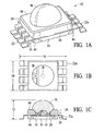
Figure 1A is a perspective view of a light emitting die package according to one embodiment of the present invention; -
Figure 1B is a top view of the light emitting die package ofFigure 1 but without lens illustrated inFigure 1A ; -
Figure 1C is a cutaway side view of the light emitting die package ofFigure 1 ; -
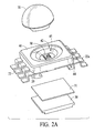
Figure 2A is an exploded perspective view of the light emitting die package ofFigure 1 ; -
Figure 2B is a exploded cutaway side view of the light emitting die package ofFigure 1 ; -
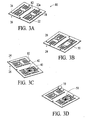
Figures 3A through 3D are perspective illustrations of a light emitting die package at various stages of its manufacturing process; and -
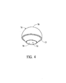
Figure 4 is a perspective view of a lens according to one embodiment of the present invention. - The present invention will now be described with reference to the
Figures 1A through 4 , which illustrate various embodiments of the present invention. In the Figures, some sizes of structures or portions are exaggerated relative to sizes of other structures or portions for illustrative purposes and, thus, are provided to illustrate the general structures of the present invention. Furthermore, various aspects of the present invention are described with reference to a structure or a portion being formed on other structures, portions, or both. As will be appreciated by those of skill in the art, references to a structure being formed "on" or "above" another structure or portion contemplates that additional structure, portion, or both may intervene. References to a structure or a portion being formed "on" another structure or portion without an intervening structure or portion are described herein as being formed "directly on" the structure or portion. - Furthermore, relative terms such as "on" or "above" are used herein to describe one structure's or portion's relationship to another structure or portion as illustrated in the Figures. It will be understood that relative terms such as "on" or "above" are intended to encompass different orientations of the device in addition to the orientation depicted in the Figures. For example, if the device in the Figures is turned over, structure or portion described as "above" other structures or portions would now be oriented "below" the other structures or portions. Likewise, if the device in the Figures is rotated along an axis, structure or portion described as "above" other structures or portions would now be oriented "next to" or "left of" the other structures or portions. Like numbers refer to like elements throughout.
- As shown in the figures for the purposes of illustration, embodiments of the present invention are exemplified by a light emitting die package including a leadframe and molded body integrated with portions of the leadframe. At least one light emitting device (LED) such as a light emitting diode is mounted on the leadframe. The molded body has an opening that surrounds the LED and has latches for latching a heatsink. The LED is covered by an encapsulant that substantially fills the opening.
- The molded body is made of high temperature plastic providing structural support to relatively thin leadframe. The LED is mounted on a main lead of the leadframe and is connected by bond wires to other leads for additional electrical connections.
- A lens coupled to the molded body above the opening to provide optical functions for light generated by the LED. As discussed in more detail below, the lens occupies much of the opening around the LED thus reducing the amount of encapsulant used within the package. This alleviates the differential thermo stress problems associated with the volumetric expansion and contraction of the encapsulant discussed above, leading to lower failure rates and relatively higher reliability.
- A heatsink is coupled to the leadframe, using the latches, to further aid in heat dissipation. The latch design allows for simpler and less costly manufacture of the die package.
-
Figure 1A is a perspective view of a light emittingdie package 10 according to one embodiment of the present invention.Figure 1B is a top view of the light emittingdie package 10 illustrated without lens and without light emitting devices both of which are illustrated inFigure 1A. Figure 1C is a cutaway side view of the light emittingdie package 10.Figure 2A is an exploded perspective view of the light emittingdie package 10.Figure 2B is an exploded cutaway side view of the light emittingdie package 10. - Referring to
Figures 1A through 2B , the light emittingdie package 10 includes aleadframe 20 including a plurality of leads, collectively referred to as leads 22. In the Figures, to avoid clutter, not all the illustrated leads are designated with thereference number 22. The leadframe has atop side 24 and abottom side 26. Theleadframe 20 is made of metal or other electrically conductive material having a predetermined thickness that can vary greatly depending on the desired characteristics and application. For example, the thickness of theleadframe 20 may be in the order of tens or hundreds of microns. - A portion of the
leadframe 20 such as afirst lead 22a, generally in the center, defines a mountingpad 28 on which a light emitting device (LED)assembly 50 is mounted. The light emitting device (LED)assembly 50 includes at least one light emitting device (LED) such as a light emitting diode. - A molded
body 40 is integrated with portions of theleadframe 20 in that an upper portion of the moldedbody 40 is above theleadframe 20 while a lower portion of the same moldedbody 40 is below theleadframe 20. In the illustrated sample embodiment, the moldedbody 40 covers a significant portion of theleadframe 20. The upper portion of the moldedbody 40 defines anopening 42 surrounding the mountingpad 28. The lower portion of the moldedbody 40 includeslatches 44. Aheatsink 30 can be attached to theleadframe 20 by engaging thelatches 44. - The
heatsink 30, when engaged to theleadframe 20, draws heat generated by theLED assembly 50 when energized and aids in dissipation of the generated heat. To avoid electrical shorts, theheatsink 30 is made of dielectric material. Alternatively, if theheatsink 30 is made using electrically conductive material, then theheatsink 30 can be separated from the leadframe by adielectric layer 31. Thedielectric layer 31 can be, for example, glass or organic polymer filled with highly thermally conductive ceramics. - A
lens 70 is coupled to the moldedbody 40 at itsopening 42 and over theLED assembly 50. The moldedbody 40 can be injection molded onto and around theleadframe 20 using high temperature plastic. Material for the moldedbody 40 is known in the art. The moldedbody 40 can be injection molded onto and around theleadframe 20 using high temperature plastics. Examples of the material for the moldedbody 40 are LCP (Liquid Crystal Polymers) filled with glass or carbon fibers. - The
lens 70 can be rigidly attached to the moldedbody 40 by an adhesive or by mechanical means at itsopening 42 and over theLED assembly 50. Alternatively, the lens can couple to the moldedbody 40 by the soft encapsulant adhesive such that the lens is allowed to float on the moldedbody 40 as the temperature rises or falls. - The
heatsink 30 is typically made of thermally conductive materials such as, for example, copper, aluminum, or ceramics. - Size of the light emitting
die package 10 can vary widely depending on its desired characteristics and application. In the illustrated embodiment, the dimensions of the light emittingdie package 10 can be in the order of a few millimeters (mm) or tens of millimeters. For example, the light emittingdie package 10 can have the following dimensions:thickness 12 ranging from approximately 3 mm to approximately 50 mm;length 14 ranging from approximately 5 mm to approximately 40 mm; andwidth 16 ranging from approximately 5 mm to approximately 30 mm. - A method of manufacturing the light emitting
die package 10 ofFigure 1A can be discussed usingFigures 3A to 3D. Figures 3A through 3D are perspective illustrations of the light emittingdie package 10 at various stages of its manufacturing process. To manufacture the light emittingdie package 10 ofFigure 1A , aleadframe strip 80 is fabricated. For illustratively purposes, inFigure 3A , theleadframe strip 80 is fabricated for manufacturing of two light emitting die packages. In fact, a leadframe strip can be fabricated to manufacture multiple light emitting die packages simultaneously. - Referring to
Figures 3A through 3D , theleadframe strip 80 includes a plurality ofleads 22 and acrossbar 82 surrounding and supporting the leads 22. Theleadframe strip 80 and theleads 22 have a top side 24 (that is the same side as thetop side 24 ofleadframe 20 ofFigures 1A to 2B ) and a bottom side 26 (that is the same side as thebottom side 26 ofleadframe 20 ofFigures 1A to 2B ). As also illustrated inFigure 1B , a portion of afirst lead 22a defines the mountingpad 28. Theleadframe strip 80 is fabricated by stamping a sheet of electrically conductive material such as metal. The thickness of the material may vary greatly depending on the desired application, for example, the thickness may range in tens or hundreds of microns (1 micron ≙ 10-6 m). Alternately, theleadframe strip 80 can be fabricated using a chemical etching or milling processes. - The molded
body 40 is molded and integrated with portions of theleadframe strip 80 and theheatsink 30. The moldedbody 40 defines theopening 42 surrounding the mountingpad 28. Further, the moldedbody 40 includes thelatches 44 on thebottom side 26 of theleadframe 20. - Before molding the
body 40 is integrated with theleadframe strip 80, theheatsink 30 can be attached to theleadframe strip 80 with a dielectric adhesive film as discussed above and as illustrated inFigure 3B . The moldedplastic body 40, when molded onto theleadframe strip 80, locks theheatsink 30 using thelatches 44 as illustrated, for example, inFigure 1A . - Then, as also illustrated in
Figures 2A and2B , theLED assembly 50 including at least one light emitting device is mounted on the mountingpad 28. Next, theLED assembly 50 is encapsulated by an encapsulant such as soft silicone or any visco-elastic polymer of low durometer or hardness. Thelens 70 is then coupled to the moldedbody 40 over theopening 42 thereby defining an enclosedoptical cavity 45 illustrated, for example, inFigures 1C and2B . - The
optical cavity 45 ofFigures 1C and2B , is substantially filled with the encapsulant. Depending on the desired results, thecavity 45 can be completely filled or partially filled while leaving an expansion space or free space behind or under the reflector of the lens, the expansion space being free of the encapsulant. Then, thecrossbar 82 portion of theleadframe strip 80 is separated leaving the leadframe frame diepackage 10 with external portions ofleads 22 sticking out of the moldedbody 40. Finally, the external portions of theleads 22 are bent to a gull-wing shape as illustrated, for example, inFigures 1A and 1C . - The
lens 70 is illustrated inFigures 1A, 1C ,2A ,2B ,3D , and4 . In particular,Figures 2A ,3D , and4 illustrate perspective views of thelens 70 andFigures 1C and2B illustrate cutaway side view of thelens 70. Referring to these illustrations of thelens 70 but more particularly toFigures 2B and4 , in the illustrated embodiment, thelens 70 includes two portions - anupper portion 75 and alower portion 77. Theupper portion 75 includes anoptical surface 76 affecting optical performance of thedie package 10. - The
lower portion 77 includes aconcave bottom surface 72, placed over theLED assembly 50, adapted to receive light from theLED assembly 50. Furthermore, thelower portion 77 definesconcave cavity 78 in its central portion to provide space for theLED assembly 50. Theconcave cavity 78, in combination with theleadframe 20, forms the enclosedoptical cavity 45 as discussed above. - The
concave bottom surface 72 of thelens 70 can be coated with optical material intended to influence or change the nature of the light emitted by the LED chip(s) before it leaves thedie package 10. Examples of types of optical materials are luminescence converting phosphors, dyes, fluorescent polymers or other materials which absorb some of the light emitted by the chip(s) and re-emit light of different wavelengths. Examples of other optical materials are light diffusants (such as Titanium oxides) or void which disperse or scatter light. Any individual or combination of these materials can be applied on the lens to obtain certain spectral and luminous performance. - Also included in the
lower portion 77 is an outerreflective surface 74 coated with reflective material. The outerreflective surface 74 is adapted to collect and to reflect the received light from theLED assembly 50. The outerreflective surface 74 is coated with reflective material such as, for example, silver, gold, or Aluminum. The reflected light leaves thelens 70 through theoptical surface 76. The reflective material can be applied to the outerreflective surface 74 by chemical deposition, printing and curing of metal paste using thick film technology. - The
reflective surface 74 can be placed at an angle that is greater thancritical angle 71 to provide a total internal reflection (TIR) for at least a portion of the light emitting by theLED assembly 50. Further, thereflective surface 74 can be fabricated to have a predetermined optical finish adopted to scatter the light in order to mix the light emitted by different color LED chips placed inside the optical cavity. For placement of thelens 70 on the rest of the light emittingdie package 10, thelens 70 may include aledge 73. - The
lower portion 77 of thelens 70 occupies much (perhaps even more than 50%) of theopening 42 that surrounds theLED assembly 50. Consequently, spatial volume of theopening 42 that would have been filled by encapsulant in prior art designs is reduced. The reduction spatial volume of theopening 42 reduces the amount of the encapsulant used to fill the volume. The reduction of the encapsulant alleviates the differential thermal stress problems associated with the volumetric expansion and contraction of the encapsulant discussed above. Consequently, thepackage 10 of the present invention has lower failure rates and relatively higher reliability. - The
lens 70 can be attached to the moldedbody 40 in a number of ways. For example, thelens 70 is adhered to the encapsulant such that thelens 70 sits on and floats on the encapsulant during temperature cycles. Alternatively, thelens 70 is fixed at itsledge 73 to the moldedbody 40. A small gap, the expansion space, of few hundreds of microns (1 micron ≙ 10-6 m) exists between lowest point of thelens 70 and thetop side 24 of theleadframe 22. This gap allows the encapsulant to breathe (expand and contract) through this gap during temperature cycles such that little, if any, high thermal stresses is experienced by other portions of thedie package 10. This reduces failure by delamination, cracking, and other causes related to thermal related stresses. - The
optical surface 76 is a portion of outer surface of the compositeoptical lens 70. Light (both reflected light and non-reflected light) from theLED assembly 50 leave the compositeoptical lens 70 through theoptical surface 76. Thelens 70 is made of optical plastic, glass, or both usually clear to allow most of the light from theLED assembly 50 to pass through thelens 70. - From the foregoing, it will be apparent that the present invention is novel and offers advantages over the current art. Although specific embodiments of the invention are described and illustrated above, the invention is not to be limited to the specific forms or arrangements of parts so described and illustrated. For example, differing configurations, sizes, or materials may be used to practice the present invention. The invention is limited by the claims that follow.
Claims (14)
- A light emitting die package (10) comprising:a leadframe (20) including a plurality of leads (22), said leadframe (20) having a top side (24) and a bottom side (26), and a portion of said leadframe (20) defining a mounting pad (28);at least one light emitting device (50) mounted on the mounting pad (28);a molded body (40) integrated with portions of said leadframe (20), said molded body (40) defining an opening (42) on the top side (24) of said leadframe (20), the opening (42) having a bottom side surrounding the mounting pad (28), the opening (42) extending from the top side (24) of the leadframe (20) to a top surface of the molded body (40), the opening (42) having a portion with angled sides tapering from a larger diameter to a smaller diameter towards the bottom side of the opening (42); anda lens (70) coupled to the molded body (40), the lens (70) extending downward beyond the light emitting device (50) so as to surround the light emitting device (50);wherein a lowest point of the lens (70) terminates above the leadframe (20) to form a gap between the top side (24) of the leadframe (20) and the lowest point of the lens (70).
- The light emitting die package (10) recited in claim 1, wherein said molded body (40) comprises a Liquid Crystal Polymer filled with glass or carbon fibers.
- The light emitting die package (10) recited in claim 1, wherein said molded body (40) includes latches (44) suitable for coupling a heatsink (30) on the bottom side (26) of said leadframe (20).
- The light emitting die package (10) recited in claim 3, further comprising said heatsink (30) coupled, via a dielectric adhesive film, to said leadframe (20), said heatsink (30) latched to said leadframe (20) by the latches (44).
- The light emitting die package (10) recited in any one of claims 1 - 4, wherein said lens (70) has a concave bottom surface (72) placed over the light emitting device (50), an outer surface (74) of said lens (70) surrounding said concave bottom surface (72) being coated with reflective material.
- The light emitting die package (10) recited in any one of claims 1 - 5, wherein said lens (70) includes a ledge (73), the lens (70) being fixed to the molded body (40) at its ledge (73), thereby providing the small gap between the lowest point of the lens (70) and the top side (24) of the leadframe (20).
- The light emitting die package (10) recited in any one of claims 1 - 6, wherein said lens (70) has a semispherical upper portion (75) and a frustoconical lower portion (77), the upper portion tapering at a ledge (73) for fitting onto the top side of the molded body (40), the frustoconical lower portion (77) fitting into and being attached to the angled sides of the opening (42) and having a concave bottom surface (72) thereby surrounding the light emitting device (50).
- The light emitting die package (10) recited in any one of claims 1 - 7, wherein said lens (70) has an upper portion (75) an a lower portion (77), the lower portion (77) fitting into the opening (42) and surrounding the light emitting device (50) on the mounting pad (28), wherein the lower portion (77) has a concave bottom surface (72) in combination with the top side (24) of the leadframe (20) forming an enclosed optical cavity (45), the enclosed optical cavity (45) being partially filled with an encapsulant.
- A method of manufacturing a light emitting die package (10), the method comprising;
fabricating a leadframe strip (80), the leadframe strip (80) including a plurality of leads (22), each lead (22) and the leadframe strip (80) having a top side (24) and a bottom side (26), portions of a first lead (22a) defining a mounting pad (28);
molding a body (40) integrated with portions of said leadframe strip (80), said molded body (40) defining an opening (42) on the top side (24) of said leadframe strip (80), the opening (42) having a bottom side surrounding the mounting pad (28), the opening (42) extending from the top side (24) of the leadframe strip (80) to a top surface of the molded body (40), the opening (42) having a portion with angled sides tapering from a larger diameter to a smaller diameter towards the bottom side of the opening (42);
mounting at least one light emitting device (50) on the mounting pad (28); and
coupling a lens (70) over the opening (42) thereby defming an optical cavity (45), the lens (70) extending downward beyond the light emitting device (50) so as to surround the light emitting device (50);
wherein a lowest point of the lens (70) terminates above the leadframe (20) to form a gap between the top side (24) of the leadframe (20) and the lowest point of the lens (70). - The method recited in claim 9, wherein the molded body (40) includes latches (44) suitable for coupling a heatsink (30) on the bottom side (26) of the leadframe strip (80), the method further comprising: coupling a heatsink (30) to the leadframe strip (80) by engaging the heatsink (30) with the latches (44).
- The method recited in claim 9 or 10 further comprising:wherein said lens (70) has a semispherical upper portion (75) and a frustoconical lower portion (77), the upper portion tapering at a ledge (73) for fitting onto the top side of the molded body (40), the frustoconical lower portion (77) fitting into and being attached to the angled sides of the opening (42) and having a concave bottom surface (72) thereby surrounding the light emitting device (50).
- The method recited in any one of claims 9 - 11, comprising:coating an outer surface (74) of said lens (70) surrounding a concave bottom surface (72) of said lens (70) with reflective material and placing said lens (70) over the light emitting device (50).
- The method recited in any one of claims 9 - 12, wherein said lens (70) includes a ledge (73), said lens (70) being fixed to the molded body (40) at its ledge thereby providing the small gap between the lowest point of the lens (70) and the top side (24) of the leadframe strip (80).
- The method recited in any of claim 12 or 13, comprising:partially filling an optical cavity (45), with encapsulant wherein said lens (70) has an upper portion (75) an a lower portion (77), the lower portion (77) fitting into the opening (42) and surrounding the light emitting device (50) on the mounting pad (28), wherein the lower portion (77) has a concave bottom surface (72) in combination with the top side (24) of the leadframe (20) forming an enclosed optical cavity (45).
Priority Applications (5)
| Application Number | Priority Date | Filing Date | Title |
|---|---|---|---|
| EP10185250.7A EP2290713B1 (en) | 2004-06-04 | 2005-06-03 | Light emitting die package with lens |
| EP10185238.2A EP2287926B1 (en) | 2004-06-04 | 2005-06-03 | Light Emitting Die Package |
| EP20100185257 EP2287929B1 (en) | 2004-06-04 | 2005-06-03 | Power light emitting diode package with reflecting lens |
| EP10185255.6A EP2287928B1 (en) | 2004-06-04 | 2005-06-03 | Power light emitting die package with reflecting lens |
| EP10185245.7A EP2287927B1 (en) | 2004-06-04 | 2005-06-03 | Power light emitting die package with lens |
Applications Claiming Priority (2)
| Application Number | Priority Date | Filing Date | Title |
|---|---|---|---|
| US10/861,929 US7456499B2 (en) | 2004-06-04 | 2004-06-04 | Power light emitting die package with reflecting lens and the method of making the same |
| EP05758018A EP1756879B1 (en) | 2004-06-04 | 2005-06-03 | Power light emitting die package with reflecting lens and the method of making the same |
Related Parent Applications (2)
| Application Number | Title | Priority Date | Filing Date |
|---|---|---|---|
| EP05758018A Division EP1756879B1 (en) | 2004-06-04 | 2005-06-03 | Power light emitting die package with reflecting lens and the method of making the same |
| EP05758018A Previously-Filed-Application EP1756879B1 (en) | 2004-06-04 | 2005-06-03 | Power light emitting die package with reflecting lens and the method of making the same |
Related Child Applications (15)
| Application Number | Title | Priority Date | Filing Date |
|---|---|---|---|
| EP10185238.2A Division EP2287926B1 (en) | 2004-06-04 | 2005-06-03 | Light Emitting Die Package |
| EP10185238.2A Previously-Filed-Application EP2287926B1 (en) | 2004-06-04 | 2005-06-03 | Light Emitting Die Package |
| EP10185238.2A Division-Into EP2287926B1 (en) | 2004-06-04 | 2005-06-03 | Light Emitting Die Package |
| EP10185245.7A Division EP2287927B1 (en) | 2004-06-04 | 2005-06-03 | Power light emitting die package with lens |
| EP10185245.7A Previously-Filed-Application EP2287927B1 (en) | 2004-06-04 | 2005-06-03 | Power light emitting die package with lens |
| EP10185245.7A Division-Into EP2287927B1 (en) | 2004-06-04 | 2005-06-03 | Power light emitting die package with lens |
| EP10185255.6A Division EP2287928B1 (en) | 2004-06-04 | 2005-06-03 | Power light emitting die package with reflecting lens |
| EP10185255.6A Previously-Filed-Application EP2287928B1 (en) | 2004-06-04 | 2005-06-03 | Power light emitting die package with reflecting lens |
| EP10185255.6A Division-Into EP2287928B1 (en) | 2004-06-04 | 2005-06-03 | Power light emitting die package with reflecting lens |
| EP20100185257 Division EP2287929B1 (en) | 2004-06-04 | 2005-06-03 | Power light emitting diode package with reflecting lens |
| EP20100185257 Previously-Filed-Application EP2287929B1 (en) | 2004-06-04 | 2005-06-03 | Power light emitting diode package with reflecting lens |
| EP20100185257 Division-Into EP2287929B1 (en) | 2004-06-04 | 2005-06-03 | Power light emitting diode package with reflecting lens |
| EP10185250.7A Division EP2290713B1 (en) | 2004-06-04 | 2005-06-03 | Light emitting die package with lens |
| EP10185250.7A Previously-Filed-Application EP2290713B1 (en) | 2004-06-04 | 2005-06-03 | Light emitting die package with lens |
| EP10185250.7A Division-Into EP2290713B1 (en) | 2004-06-04 | 2005-06-03 | Light emitting die package with lens |
Publications (3)
| Publication Number | Publication Date |
|---|---|
| EP2075856A2 EP2075856A2 (en) | 2009-07-01 |
| EP2075856A3 EP2075856A3 (en) | 2009-07-08 |
| EP2075856B1 true EP2075856B1 (en) | 2015-05-13 |
Family
ID=35446717
Family Applications (7)
| Application Number | Title | Priority Date | Filing Date |
|---|---|---|---|
| EP10185245.7A Active EP2287927B1 (en) | 2004-06-04 | 2005-06-03 | Power light emitting die package with lens |
| EP20080161650 Active EP2075856B1 (en) | 2004-06-04 | 2005-06-03 | Power Light Emitting Die Package With Reflecting Lens And The Method Of Making The Same |
| EP20100185257 Active EP2287929B1 (en) | 2004-06-04 | 2005-06-03 | Power light emitting diode package with reflecting lens |
| EP10185255.6A Active EP2287928B1 (en) | 2004-06-04 | 2005-06-03 | Power light emitting die package with reflecting lens |
| EP10185250.7A Active EP2290713B1 (en) | 2004-06-04 | 2005-06-03 | Light emitting die package with lens |
| EP10185238.2A Active EP2287926B1 (en) | 2004-06-04 | 2005-06-03 | Light Emitting Die Package |
| EP05758018A Active EP1756879B1 (en) | 2004-06-04 | 2005-06-03 | Power light emitting die package with reflecting lens and the method of making the same |
Family Applications Before (1)
| Application Number | Title | Priority Date | Filing Date |
|---|---|---|---|
| EP10185245.7A Active EP2287927B1 (en) | 2004-06-04 | 2005-06-03 | Power light emitting die package with lens |
Family Applications After (5)
| Application Number | Title | Priority Date | Filing Date |
|---|---|---|---|
| EP20100185257 Active EP2287929B1 (en) | 2004-06-04 | 2005-06-03 | Power light emitting diode package with reflecting lens |
| EP10185255.6A Active EP2287928B1 (en) | 2004-06-04 | 2005-06-03 | Power light emitting die package with reflecting lens |
| EP10185250.7A Active EP2290713B1 (en) | 2004-06-04 | 2005-06-03 | Light emitting die package with lens |
| EP10185238.2A Active EP2287926B1 (en) | 2004-06-04 | 2005-06-03 | Light Emitting Die Package |
| EP05758018A Active EP1756879B1 (en) | 2004-06-04 | 2005-06-03 | Power light emitting die package with reflecting lens and the method of making the same |
Country Status (8)
| Country | Link |
|---|---|
| US (3) | US7456499B2 (en) |
| EP (7) | EP2287927B1 (en) |
| JP (2) | JP5596901B2 (en) |
| AT (1) | ATE420464T1 (en) |
| DE (1) | DE602005012259D1 (en) |
| MY (1) | MY139974A (en) |
| TW (2) | TWI382561B (en) |
| WO (1) | WO2005119707A2 (en) |
Families Citing this family (216)
| Publication number | Priority date | Publication date | Assignee | Title |
|---|---|---|---|---|
| US7775685B2 (en) * | 2003-05-27 | 2010-08-17 | Cree, Inc. | Power surface mount light emitting die package |
| US7244965B2 (en) | 2002-09-04 | 2007-07-17 | Cree Inc, | Power surface mount light emitting die package |
| EP1496551B1 (en) * | 2003-07-09 | 2013-08-21 | Nichia Corporation | Light emitting diode, method of manufacturing the same and lighting equipment incorporating the same |
| US7456499B2 (en) | 2004-06-04 | 2008-11-25 | Cree, Inc. | Power light emitting die package with reflecting lens and the method of making the same |
| WO2006059828A1 (en) * | 2004-09-10 | 2006-06-08 | Seoul Semiconductor Co., Ltd. | Light emitting diode package having multiple molding resins |
| TWI405349B (en) * | 2004-10-07 | 2013-08-11 | Seoul Semiconductor Co Ltd | Side-luminescence lens and luminescent device suing the same |
| US20060086945A1 (en) * | 2004-10-27 | 2006-04-27 | Harvatek Corporation | Package structure for optical-electrical semiconductor |
| US20060091414A1 (en) * | 2004-10-29 | 2006-05-04 | Ouderkirk Andrew J | LED package with front surface heat extractor |
| US7224047B2 (en) * | 2004-12-18 | 2007-05-29 | Lsi Corporation | Semiconductor device package with reduced leakage |
| US7326062B2 (en) * | 2005-02-07 | 2008-02-05 | Avago Technologies Ecbu Ip Pte Ltd | System and method for increasing the surface mounting stability of a lamp |
| US20060180909A1 (en) * | 2005-02-14 | 2006-08-17 | Irwin Kim | Optical device package |
| KR100631903B1 (en) * | 2005-02-17 | 2006-10-11 | 삼성전기주식회사 | High power LED housing and its manufacturing method |
| US20080296589A1 (en) * | 2005-03-24 | 2008-12-04 | Ingo Speier | Solid-State Lighting Device Package |
| CA2614803C (en) * | 2005-04-05 | 2015-08-25 | Tir Technology Lp | Electronic device package with an integrated evaporator |
| US7980743B2 (en) | 2005-06-14 | 2011-07-19 | Cree, Inc. | LED backlighting for displays |
| US20060289887A1 (en) * | 2005-06-24 | 2006-12-28 | Jabil Circuit, Inc. | Surface mount light emitting diode (LED) assembly with improved power dissipation |
| KR100592508B1 (en) * | 2005-07-15 | 2006-06-26 | 한국광기술원 | High power led package with beacon type substrate |
| JP2007036073A (en) * | 2005-07-29 | 2007-02-08 | Hitachi Displays Ltd | Lighting device and display unit using it |
| KR20080106402A (en) | 2006-01-05 | 2008-12-05 | 일루미텍스, 인크. | Separate optical device for directing light from an led |
| US8044412B2 (en) | 2006-01-20 | 2011-10-25 | Taiwan Semiconductor Manufacturing Company, Ltd | Package for a light emitting element |
| US8441179B2 (en) | 2006-01-20 | 2013-05-14 | Cree, Inc. | Lighting devices having remote lumiphors that are excited by lumiphor-converted semiconductor excitation sources |
| JP5102455B2 (en) * | 2006-03-06 | 2012-12-19 | Idec株式会社 | LED light emitting device |
| KR100752009B1 (en) * | 2006-03-06 | 2007-08-28 | 삼성전기주식회사 | Backlight unit provided with light emitting diodes thereon |
| US7655957B2 (en) | 2006-04-27 | 2010-02-02 | Cree, Inc. | Submounts for semiconductor light emitting device packages and semiconductor light emitting device packages including the same |
| KR100731678B1 (en) * | 2006-05-08 | 2007-06-22 | 서울반도체 주식회사 | Chip-type led package and light emitting apparatus having the same |
| WO2007135707A1 (en) | 2006-05-18 | 2007-11-29 | Nichia Corporation | Resin molded body and surface-mounted light emitting device, and manufacturing method thereof |
| EP2027602A4 (en) * | 2006-05-23 | 2012-11-28 | Cree Inc | Lighting device and method of making |
| US8610134B2 (en) * | 2006-06-29 | 2013-12-17 | Cree, Inc. | LED package with flexible polyimide circuit and method of manufacturing LED package |
| US7906794B2 (en) | 2006-07-05 | 2011-03-15 | Koninklijke Philips Electronics N.V. | Light emitting device package with frame and optically transmissive element |
| US8044418B2 (en) * | 2006-07-13 | 2011-10-25 | Cree, Inc. | Leadframe-based packages for solid state light emitting devices |
| US7960819B2 (en) * | 2006-07-13 | 2011-06-14 | Cree, Inc. | Leadframe-based packages for solid state emitting devices |
| EP2372797A3 (en) * | 2006-07-31 | 2017-01-18 | 3M Innovative Properties Co. | Light emitting diode source with hollow collection lens |
| JP5330993B2 (en) | 2006-07-31 | 2013-10-30 | スリーエム イノベイティブ プロパティズ カンパニー | Optical projection subsystem |
| US8075140B2 (en) | 2006-07-31 | 2011-12-13 | 3M Innovative Properties Company | LED illumination system with polarization recycling |
| US7909482B2 (en) | 2006-08-21 | 2011-03-22 | Innotec Corporation | Electrical device having boardless electrical component mounting arrangement |
| KR101258227B1 (en) * | 2006-08-29 | 2013-04-25 | 서울반도체 주식회사 | Light emitting device |
| EP2070123A2 (en) | 2006-10-02 | 2009-06-17 | Illumitex, Inc. | Led system and method |
| TW200820455A (en) * | 2006-10-18 | 2008-05-01 | Young Lighting Technology Corp | LED package and manufacture method thereof |
| TW200820463A (en) * | 2006-10-25 | 2008-05-01 | Lighthouse Technology Co Ltd | Light-improving SMD diode holder and package thereof |
| BRPI0718086A2 (en) * | 2006-10-31 | 2013-11-05 | Tir Technology Lp | LIGHTING DEVICE PACKAGING |
| TW200822384A (en) * | 2006-11-03 | 2008-05-16 | Coretronic Corp | LED package structure |
| CN101578711A (en) * | 2006-11-09 | 2009-11-11 | 跃进封装公司 | Leg reflective package |
| TWM312020U (en) * | 2006-12-04 | 2007-05-11 | Lighthouse Technology Co Ltd | Light emitting diode package structure |
| US20080179618A1 (en) * | 2007-01-26 | 2008-07-31 | Ching-Tai Cheng | Ceramic led package |
| TWI378580B (en) * | 2007-03-07 | 2012-12-01 | Everlight Electronics Co Ltd | Socket led device |
| US8408773B2 (en) | 2007-03-19 | 2013-04-02 | Innotec Corporation | Light for vehicles |
| US7712933B2 (en) | 2007-03-19 | 2010-05-11 | Interlum, Llc | Light for vehicles |
| JP5122172B2 (en) | 2007-03-30 | 2013-01-16 | ローム株式会社 | Semiconductor light emitting device |
| US7964888B2 (en) | 2007-04-18 | 2011-06-21 | Cree, Inc. | Semiconductor light emitting device packages and methods |
| KR100855065B1 (en) * | 2007-04-24 | 2008-08-29 | 삼성전기주식회사 | Light emitting diode package |
| JP5233170B2 (en) * | 2007-05-31 | 2013-07-10 | 日亜化学工業株式会社 | LIGHT EMITTING DEVICE, RESIN MOLDED BODY FORMING LIGHT EMITTING DEVICE, AND METHOD FOR PRODUCING THEM |
| US20090008662A1 (en) * | 2007-07-05 | 2009-01-08 | Ian Ashdown | Lighting device package |
| KR100880638B1 (en) * | 2007-07-06 | 2009-01-30 | 엘지전자 주식회사 | Light emitting device package |
| EP2201615B8 (en) * | 2007-09-20 | 2015-01-28 | Philips Intellectual Property & Standards GmbH | Led package and method for manufacturing the led package |
| US7802901B2 (en) | 2007-09-25 | 2010-09-28 | Cree, Inc. | LED multi-chip lighting units and related methods |
| TWM329864U (en) * | 2007-10-03 | 2008-04-01 | Everlight Electronics Co Ltd | Structure of light emitted diode package |
| US10256385B2 (en) | 2007-10-31 | 2019-04-09 | Cree, Inc. | Light emitting die (LED) packages and related methods |
| WO2009076579A2 (en) | 2007-12-12 | 2009-06-18 | Innotec Corporation | Overmolded circuit board and method |
| US20100133580A1 (en) * | 2008-01-02 | 2010-06-03 | Everlight Electronics Co., Ltd. | Light emitting diode package structure and conductive structure and manufacturing method thereof |
| US10008637B2 (en) | 2011-12-06 | 2018-06-26 | Cree, Inc. | Light emitter devices and methods with reduced dimensions and improved light output |
| EP2240968A1 (en) | 2008-02-08 | 2010-10-20 | Illumitex, Inc. | System and method for emitter layer shaping |
| US7855398B2 (en) * | 2008-02-28 | 2010-12-21 | Avago Technologies Ecbu Ip (Singapore) Pte. Ltd. | Ceramic light emitting device package |
| KR20090100117A (en) * | 2008-03-19 | 2009-09-23 | 삼성전자주식회사 | Backlight unit and liquid crystal display having the same |
| DE202008011979U1 (en) * | 2008-04-01 | 2008-12-11 | Lebensstil Technology Co., Ltd. | Mounting arrangement of a filament |
| JP5155890B2 (en) | 2008-06-12 | 2013-03-06 | ルネサスエレクトロニクス株式会社 | Semiconductor device and manufacturing method thereof |
| JP5217800B2 (en) | 2008-09-03 | 2013-06-19 | 日亜化学工業株式会社 | Light emitting device, resin package, resin molded body, and manufacturing method thereof |
| US10509304B2 (en) * | 2008-11-12 | 2019-12-17 | Tseng-Lu Chien | LED projection light has features |
| TW201034256A (en) * | 2008-12-11 | 2010-09-16 | Illumitex Inc | Systems and methods for packaging light-emitting diode devices |
| US8598602B2 (en) * | 2009-01-12 | 2013-12-03 | Cree, Inc. | Light emitting device packages with improved heat transfer |
| US7923739B2 (en) | 2009-06-05 | 2011-04-12 | Cree, Inc. | Solid state lighting device |
| US8269248B2 (en) * | 2009-03-02 | 2012-09-18 | Thompson Joseph B | Light emitting assemblies and portions thereof |
| US8314433B2 (en) * | 2009-03-19 | 2012-11-20 | Cid Technologies Llc | Flexible thermal energy dissipating and light emitting diode mounting arrangement |
| JP5327042B2 (en) * | 2009-03-26 | 2013-10-30 | 豊田合成株式会社 | LED lamp manufacturing method |
| US8096671B1 (en) | 2009-04-06 | 2012-01-17 | Nmera, Llc | Light emitting diode illumination system |
| US8101955B2 (en) * | 2009-04-17 | 2012-01-24 | Avago Technologies Ecbu Ip (Singapore) Pte. Ltd. | PLCC package with a reflector cup surrounded by an encapsulant |
| US8089075B2 (en) * | 2009-04-17 | 2012-01-03 | Avago Technologies Ecbu Ip (Singapore) Pte. Ltd. | LFCC package with a reflector cup surrounded by a single encapsulant |
| US8957435B2 (en) * | 2009-04-28 | 2015-02-17 | Cree, Inc. | Lighting device |
| US8686445B1 (en) | 2009-06-05 | 2014-04-01 | Cree, Inc. | Solid state lighting devices and methods |
| US8860043B2 (en) * | 2009-06-05 | 2014-10-14 | Cree, Inc. | Light emitting device packages, systems and methods |
| US9111778B2 (en) | 2009-06-05 | 2015-08-18 | Cree, Inc. | Light emitting diode (LED) devices, systems, and methods |
| CN101936500A (en) * | 2009-06-30 | 2011-01-05 | 富准精密工业(深圳)有限公司 | Light-emitting diode module |
| US8476812B2 (en) * | 2009-07-07 | 2013-07-02 | Cree, Inc. | Solid state lighting device with improved heatsink |
| US7932532B2 (en) * | 2009-08-04 | 2011-04-26 | Cree, Inc. | Solid state lighting device with improved heatsink |
| US8449128B2 (en) | 2009-08-20 | 2013-05-28 | Illumitex, Inc. | System and method for a lens and phosphor layer |
| US8585253B2 (en) | 2009-08-20 | 2013-11-19 | Illumitex, Inc. | System and method for color mixing lens array |
| US8410371B2 (en) | 2009-09-08 | 2013-04-02 | Cree, Inc. | Electronic device submounts with thermally conductive vias and light emitting devices including the same |
| CN102024882A (en) * | 2009-09-14 | 2011-04-20 | 展晶科技(深圳)有限公司 | LED device and manufacturing method thereof |
| US20110062470A1 (en) * | 2009-09-17 | 2011-03-17 | Koninklijke Philips Electronics N.V. | Reduced angular emission cone illumination leds |
| US8120056B2 (en) * | 2009-10-19 | 2012-02-21 | Avago Technologies Ecbu Ip (Singapore) Pte. Ltd. | Light emitting diode assembly |
| JP5263788B2 (en) * | 2009-10-22 | 2013-08-14 | シャープ株式会社 | Display device |
| US7893445B2 (en) * | 2009-11-09 | 2011-02-22 | Cree, Inc. | Solid state emitter package including red and blue emitters |
| WO2011060319A1 (en) | 2009-11-13 | 2011-05-19 | Uni-Light Llc | Led thermal management |
| KR101285311B1 (en) | 2009-12-29 | 2013-07-11 | 일진엘이디(주) | LED package and back light unit |
| US9024350B2 (en) * | 2010-02-08 | 2015-05-05 | Ban P Loh | LED light module |
| TW201128763A (en) * | 2010-02-11 | 2011-08-16 | Gem Weltronics Twn Corp | Multilayer array type light-emitting diode |
| TW201128764A (en) * | 2010-02-11 | 2011-08-16 | Gem Weltronics Twn Corp | Method for packaging multilayer array-type light-emitting diode |
| US7888852B1 (en) * | 2010-02-22 | 2011-02-15 | Wen-Kung Sung | LED heat dissipation structure |
| US8508127B2 (en) * | 2010-03-09 | 2013-08-13 | Cree, Inc. | High CRI lighting device with added long-wavelength blue color |
| US8338851B2 (en) * | 2010-03-17 | 2012-12-25 | GEM Weltronics TWN Corporation | Multi-layer LED array engine |
| US9240526B2 (en) | 2010-04-23 | 2016-01-19 | Cree, Inc. | Solid state light emitting diode packages with leadframes and ceramic material |
| US8581382B2 (en) * | 2010-06-18 | 2013-11-12 | Stats Chippac Ltd. | Integrated circuit packaging system with leadframe and method of manufacture thereof |
| US8648359B2 (en) | 2010-06-28 | 2014-02-11 | Cree, Inc. | Light emitting devices and methods |
| US8269244B2 (en) | 2010-06-28 | 2012-09-18 | Cree, Inc. | LED package with efficient, isolated thermal path |
| USD643819S1 (en) | 2010-07-16 | 2011-08-23 | Cree, Inc. | Package for light emitting diode (LED) lighting |
| US8896005B2 (en) * | 2010-07-29 | 2014-11-25 | Cree, Inc. | Lighting devices that comprise one or more solid state light emitters |
| EP2437581A1 (en) | 2010-09-30 | 2012-04-04 | Odelo GmbH | Light diode on a ceramic substrate basis |
| DE102010047002A1 (en) | 2010-09-30 | 2012-04-05 | Odelo Gmbh | Method for producing belinster SMD LEDs |
| US9140429B2 (en) | 2010-10-14 | 2015-09-22 | Cree, Inc. | Optical element edge treatment for lighting device |
| US20130015567A1 (en) * | 2010-10-21 | 2013-01-17 | Panasonic Corporation | Semiconductor device and production method for same |
| US9648673B2 (en) | 2010-11-05 | 2017-05-09 | Cree, Inc. | Lighting device with spatially segregated primary and secondary emitters |
| US8491140B2 (en) | 2010-11-05 | 2013-07-23 | Cree, Inc. | Lighting device with multiple emitters and remote lumiphor |
| US8556469B2 (en) * | 2010-12-06 | 2013-10-15 | Cree, Inc. | High efficiency total internal reflection optic for solid state lighting luminaires |
| US8610140B2 (en) | 2010-12-15 | 2013-12-17 | Cree, Inc. | Light emitting diode (LED) packages, systems, devices and related methods |
| USD679842S1 (en) | 2011-01-03 | 2013-04-09 | Cree, Inc. | High brightness LED package |
| US8772817B2 (en) | 2010-12-22 | 2014-07-08 | Cree, Inc. | Electronic device submounts including substrates with thermally conductive vias |
| TW201251140A (en) | 2011-01-31 | 2012-12-16 | Cree Inc | High brightness light emitting diode (LED) packages, systems and methods with improved resin filling and high adhesion |
| CN103348496A (en) | 2011-02-07 | 2013-10-09 | 克利公司 | Components and methods for light emitting diode (LED) lighting |
| US10098197B2 (en) | 2011-06-03 | 2018-10-09 | Cree, Inc. | Lighting devices with individually compensating multi-color clusters |
| KR101803001B1 (en) * | 2011-03-11 | 2017-12-28 | 서울반도체 주식회사 | Led channel letter and led module useful for the same |
| US10074779B2 (en) * | 2011-03-11 | 2018-09-11 | Seoul Semiconductor Co., Ltd. | LED module, method for manufacturing the same, and LED channel letter including the same |
| JP5456077B2 (en) * | 2011-03-11 | 2014-03-26 | ソウル セミコンダクター カンパニー リミテッド | LED module, manufacturing method thereof, and LED channel letter including LED module |
| US8405181B2 (en) * | 2011-03-16 | 2013-03-26 | Intellectual Discovery Co., Ltd. | High brightness and high contrast plastic leaded chip carrier LED |
| US20120256205A1 (en) * | 2011-04-06 | 2012-10-11 | Tek Beng Low | Led lighting module with uniform light output |
| DE102011100028A1 (en) * | 2011-04-29 | 2012-10-31 | Osram Opto Semiconductors Gmbh | Component and method for manufacturing a device |
| US8921875B2 (en) | 2011-05-10 | 2014-12-30 | Cree, Inc. | Recipient luminophoric mediums having narrow spectrum luminescent materials and related semiconductor light emitting devices and methods |
| US8729790B2 (en) | 2011-06-03 | 2014-05-20 | Cree, Inc. | Coated phosphors and light emitting devices including the same |
| US8814621B2 (en) | 2011-06-03 | 2014-08-26 | Cree, Inc. | Methods of determining and making red nitride compositions |
| US8906263B2 (en) | 2011-06-03 | 2014-12-09 | Cree, Inc. | Red nitride phosphors |
| US8747697B2 (en) | 2011-06-07 | 2014-06-10 | Cree, Inc. | Gallium-substituted yttrium aluminum garnet phosphor and light emitting devices including the same |
| US20120314419A1 (en) * | 2011-06-08 | 2012-12-13 | Wen-Kung Sung | Heat dissipation structure of light-emitting diode |
| KR101850980B1 (en) * | 2011-06-08 | 2018-05-31 | 서울반도체 주식회사 | Light emitting diode package |
| US8684569B2 (en) | 2011-07-06 | 2014-04-01 | Cree, Inc. | Lens and trim attachment structure for solid state downlights |
| US10686107B2 (en) | 2011-07-21 | 2020-06-16 | Cree, Inc. | Light emitter devices and components with improved chemical resistance and related methods |
| JP2014525146A (en) | 2011-07-21 | 2014-09-25 | クリー インコーポレイテッド | Light emitting device, package, component, and method for improved chemical resistance and related methods |
| US10211380B2 (en) | 2011-07-21 | 2019-02-19 | Cree, Inc. | Light emitting devices and components having improved chemical resistance and related methods |
| DE102012107547B4 (en) * | 2011-08-22 | 2020-12-31 | Samsung Electronics Co., Ltd. | Housing for a light emitting device |
| CN103782403B (en) | 2011-09-06 | 2017-06-30 | 克利公司 | Optical transmitting set packaging part and device and correlation technique with improved wire bonding |
| KR102010099B1 (en) * | 2011-09-16 | 2019-10-21 | 에어 모션 시스템즈, 인크. | Assembly and interconnection method for high-power led devices |
| US8710538B2 (en) * | 2011-10-05 | 2014-04-29 | Avago Technologies General Ip (Singapore) Pte. Ltd. | Light-emitting device with a spacer at bottom surface |
| US9496466B2 (en) | 2011-12-06 | 2016-11-15 | Cree, Inc. | Light emitter devices and methods, utilizing light emitting diodes (LEDs), for improved light extraction |
| US9318669B2 (en) | 2012-01-30 | 2016-04-19 | Cree, Inc. | Methods of determining and making red nitride compositions |
| US9343441B2 (en) | 2012-02-13 | 2016-05-17 | Cree, Inc. | Light emitter devices having improved light output and related methods |
| US9240530B2 (en) | 2012-02-13 | 2016-01-19 | Cree, Inc. | Light emitter devices having improved chemical and physical resistance and related methods |
| US9735198B2 (en) | 2012-03-30 | 2017-08-15 | Cree, Inc. | Substrate based light emitter devices, components, and related methods |
| DE112013002944T5 (en) | 2012-06-13 | 2015-02-19 | Innotec, Corp. | Flexible hollow fiber optic cable |
| WO2013190871A1 (en) * | 2012-06-20 | 2013-12-27 | アオイ電子株式会社 | Light source-integrated optical sensor |
| KR101371134B1 (en) | 2012-10-31 | 2014-03-07 | 부국전자 주식회사 | Led package |
| US9316382B2 (en) | 2013-01-31 | 2016-04-19 | Cree, Inc. | Connector devices, systems, and related methods for connecting light emitting diode (LED) modules |
| TWI511339B (en) * | 2013-02-06 | 2015-12-01 | Lite On Electronics Guangzhou | Led package and lead frame thereof |
| US9039746B2 (en) | 2013-02-08 | 2015-05-26 | Cree, Inc. | Solid state light emitting devices including adjustable melatonin suppression effects |
| US9030103B2 (en) | 2013-02-08 | 2015-05-12 | Cree, Inc. | Solid state light emitting devices including adjustable scotopic / photopic ratio |
| US9565782B2 (en) | 2013-02-15 | 2017-02-07 | Ecosense Lighting Inc. | Field replaceable power supply cartridge |
| TWI469113B (en) * | 2013-02-25 | 2015-01-11 | Elumina Technology Inc | Led color point-light source being applied to dot-matrix advertisement board |
| US9587790B2 (en) | 2013-03-15 | 2017-03-07 | Cree, Inc. | Remote lumiphor solid state lighting devices with enhanced light extraction |
| JP5904671B2 (en) * | 2013-03-19 | 2016-04-20 | 京セラコネクタプロダクツ株式会社 | Luminaire provided with semiconductor light emitting device |
| US9608177B2 (en) * | 2013-08-27 | 2017-03-28 | Lumens Co., Ltd. | Light emitting device package and backlight unit having the same |
| CN105706237B (en) * | 2013-09-13 | 2019-10-18 | 亮锐控股有限公司 | The encapsulation based on frame for flip-chip LED |
| US9240528B2 (en) | 2013-10-03 | 2016-01-19 | Cree, Inc. | Solid state lighting apparatus with high scotopic/photopic (S/P) ratio |
| US9976710B2 (en) | 2013-10-30 | 2018-05-22 | Lilibrand Llc | Flexible strip lighting apparatus and methods |
| CN111063787A (en) * | 2014-01-23 | 2020-04-24 | 亮锐控股有限公司 | Light emitting device with self-aligned preformed lens |
| WO2015187388A1 (en) | 2014-06-02 | 2015-12-10 | 3M Innovative Properties Company | Led with remote phosphor and shell reflector |
| US9775199B2 (en) | 2014-07-31 | 2017-09-26 | GE Lighting Solutions, LLC | Light emitting diode retrofit lamp for high intensity discharge ballast |
| US10477636B1 (en) | 2014-10-28 | 2019-11-12 | Ecosense Lighting Inc. | Lighting systems having multiple light sources |
| US9989240B2 (en) | 2014-12-03 | 2018-06-05 | GE Lighting Solutions, LLC | LED lamps for retrofit on high wattage metal halide ballasts |
| US10431568B2 (en) | 2014-12-18 | 2019-10-01 | Cree, Inc. | Light emitting diodes, components and related methods |
| US11306897B2 (en) | 2015-02-09 | 2022-04-19 | Ecosense Lighting Inc. | Lighting systems generating partially-collimated light emissions |
| US9869450B2 (en) | 2015-02-09 | 2018-01-16 | Ecosense Lighting Inc. | Lighting systems having a truncated parabolic- or hyperbolic-conical light reflector, or a total internal reflection lens; and having another light reflector |
| US9746159B1 (en) | 2015-03-03 | 2017-08-29 | Ecosense Lighting Inc. | Lighting system having a sealing system |
| US9568665B2 (en) | 2015-03-03 | 2017-02-14 | Ecosense Lighting Inc. | Lighting systems including lens modules for selectable light distribution |
| US9651227B2 (en) | 2015-03-03 | 2017-05-16 | Ecosense Lighting Inc. | Low-profile lighting system having pivotable lighting enclosure |
| US9651216B2 (en) | 2015-03-03 | 2017-05-16 | Ecosense Lighting Inc. | Lighting systems including asymmetric lens modules for selectable light distribution |
| US20160293811A1 (en) | 2015-03-31 | 2016-10-06 | Cree, Inc. | Light emitting diodes and methods with encapsulation |
| EP3289281A1 (en) | 2015-04-30 | 2018-03-07 | Cree, Inc. | Solid state lighting components |
| USD785218S1 (en) | 2015-07-06 | 2017-04-25 | Ecosense Lighting Inc. | LED luminaire having a mounting system |
| US10074635B2 (en) | 2015-07-17 | 2018-09-11 | Cree, Inc. | Solid state light emitter devices and methods |
| USD782093S1 (en) | 2015-07-20 | 2017-03-21 | Ecosense Lighting Inc. | LED luminaire having a mounting system |
| USD782094S1 (en) | 2015-07-20 | 2017-03-21 | Ecosense Lighting Inc. | LED luminaire having a mounting system |
| DE102015112042B4 (en) * | 2015-07-23 | 2021-07-01 | OSRAM Opto Semiconductors Gesellschaft mit beschränkter Haftung | Optoelectronic lighting device |
| US9651232B1 (en) | 2015-08-03 | 2017-05-16 | Ecosense Lighting Inc. | Lighting system having a mounting device |
| US10132476B2 (en) | 2016-03-08 | 2018-11-20 | Lilibrand Llc | Lighting system with lens assembly |
| CN109791968A (en) | 2016-07-26 | 2019-05-21 | 克利公司 | Light emitting diode, component and correlation technique |
| DE102016113942A1 (en) | 2016-07-28 | 2018-02-15 | HELLA GmbH & Co. KGaA | Light source with a primary optic of silicone and method for producing the light source |
| WO2018052902A1 (en) | 2016-09-13 | 2018-03-22 | Cree, Inc. | Light emitting diodes, components and related methods |
| DE102016011320B3 (en) * | 2016-09-21 | 2017-08-24 | Azur Space Solar Power Gmbh | Lens, solar cell unit and joining method for a solar cell unit |
| US10804251B2 (en) | 2016-11-22 | 2020-10-13 | Cree, Inc. | Light emitting diode (LED) devices, components and methods |
| CN110998880A (en) | 2017-01-27 | 2020-04-10 | 莉莉布兰德有限责任公司 | Illumination system with high color rendering index and uniform planar illumination |
| US10439114B2 (en) | 2017-03-08 | 2019-10-08 | Cree, Inc. | Substrates for light emitting diodes and related methods |
| US20180328552A1 (en) | 2017-03-09 | 2018-11-15 | Lilibrand Llc | Fixtures and lighting accessories for lighting devices |
| US10410997B2 (en) | 2017-05-11 | 2019-09-10 | Cree, Inc. | Tunable integrated optics LED components and methods |
| US10672957B2 (en) | 2017-07-19 | 2020-06-02 | Cree, Inc. | LED apparatuses and methods for high lumen output density |
| US11107857B2 (en) | 2017-08-18 | 2021-08-31 | Creeled, Inc. | Light emitting diodes, components and related methods |
| US11101248B2 (en) | 2017-08-18 | 2021-08-24 | Creeled, Inc. | Light emitting diodes, components and related methods |
| US10361349B2 (en) | 2017-09-01 | 2019-07-23 | Cree, Inc. | Light emitting diodes, components and related methods |
| CN109427698B (en) * | 2017-09-04 | 2023-08-29 | 恩智浦美国有限公司 | Method for assembling QFP type semiconductor device |
| WO2019090077A1 (en) * | 2017-11-03 | 2019-05-09 | Innotec, Corp. | Illuminated optical device |
| US10541353B2 (en) | 2017-11-10 | 2020-01-21 | Cree, Inc. | Light emitting devices including narrowband converters for outdoor lighting applications |
| US10734560B2 (en) | 2017-11-29 | 2020-08-04 | Cree, Inc. | Configurable circuit layout for LEDs |
| WO2019151826A1 (en) * | 2018-02-05 | 2019-08-08 | 엘지이노텍 주식회사 | Semiconductor device package and light emitting device comprising same |
| KR102487358B1 (en) * | 2018-02-05 | 2023-01-11 | 엘지이노텍 주식회사 | Semiconductor device package and light emitting device including the same |
| KR102528379B1 (en) * | 2018-02-05 | 2023-05-03 | 엘지이노텍 주식회사 | Semiconductor device package and light emitting device including the same |
| US10573543B2 (en) | 2018-04-30 | 2020-02-25 | Cree, Inc. | Apparatus and methods for mass transfer of electronic die |
| WO2019213299A1 (en) | 2018-05-01 | 2019-11-07 | Lilibrand Llc | Lighting systems and devices with central silicone module |
| US11024785B2 (en) | 2018-05-25 | 2021-06-01 | Creeled, Inc. | Light-emitting diode packages |
| US11101410B2 (en) | 2018-05-30 | 2021-08-24 | Creeled, Inc. | LED systems, apparatuses, and methods |
| US10453827B1 (en) | 2018-05-30 | 2019-10-22 | Cree, Inc. | LED apparatuses and methods |
| EP3776674A1 (en) | 2018-06-04 | 2021-02-17 | Cree, Inc. | Led apparatuses, and method |
| US10964866B2 (en) | 2018-08-21 | 2021-03-30 | Cree, Inc. | LED device, system, and method with adaptive patterns |
| US11233183B2 (en) | 2018-08-31 | 2022-01-25 | Creeled, Inc. | Light-emitting diodes, light-emitting diode arrays and related devices |
| US11335833B2 (en) | 2018-08-31 | 2022-05-17 | Creeled, Inc. | Light-emitting diodes, light-emitting diode arrays and related devices |
| WO2020131933A1 (en) | 2018-12-17 | 2020-06-25 | Lilibrand Llc | Strip lighting systems which comply with ac driving power |
| US11101411B2 (en) | 2019-06-26 | 2021-08-24 | Creeled, Inc. | Solid-state light emitting devices including light emitting diodes in package structures |
| US10724720B1 (en) | 2019-09-16 | 2020-07-28 | Elemental LED, Inc. | Multi-purpose channels for linear lighting |
| US10724719B1 (en) * | 2019-09-16 | 2020-07-28 | Elemental LED, Inc. | Channel system for linear lighting |
| TWI747113B (en) | 2019-12-23 | 2021-11-21 | 瑞軒科技股份有限公司 | Light-emitting diode device and display device |
| US11118752B2 (en) | 2020-01-27 | 2021-09-14 | Elemental LED, Inc. | Flexible cover for linear lighting channels |
| CA3198849A1 (en) * | 2020-10-29 | 2022-05-05 | Bitro Group, Inc. | Led lighting device |
Family Cites Families (102)
| Publication number | Priority date | Publication date | Assignee | Title |
|---|---|---|---|---|
| JPS48102585A (en) * | 1972-04-04 | 1973-12-22 | ||
| US4267559A (en) | 1979-09-24 | 1981-05-12 | Bell Telephone Laboratories, Incorporated | Low thermal impedance light-emitting diode package |
| JPS60103841A (en) | 1983-11-11 | 1985-06-08 | Toshiba Corp | Repeater |
| JPS60103841U (en) * | 1983-12-19 | 1985-07-15 | ソニー株式会社 | electronic parts equipment |
| JPS60158604A (en) | 1984-01-27 | 1985-08-20 | Ricoh Co Ltd | Metal oxide magnetic substance and magnetic film |
| JPH0789681B2 (en) | 1984-07-31 | 1995-09-27 | 財団法人鉄道総合技術研究所 | Levitation coil displacement detector |
| JPS61125066A (en) | 1984-11-22 | 1986-06-12 | Hitachi Ltd | Semiconductor device |
| JPS62229701A (en) * | 1986-03-31 | 1987-10-08 | 株式会社小糸製作所 | Lamp apparatus for vehicle |
| JPS63131157A (en) | 1986-11-21 | 1988-06-03 | Canon Inc | Electrostatic discharging device |
| US5043716A (en) * | 1988-07-14 | 1991-08-27 | Adaptive Micro Systems, Inc. | Electronic display with lens matrix |
| EP1022787B2 (en) * | 1989-05-31 | 2012-07-11 | OSRAM Opto Semiconductors GmbH | Method of producing a surface-mountable optical element and surface-mountable optical element |
| JPH0388472A (en) | 1989-06-29 | 1991-04-12 | Shimadzu Corp | Hand-written communication terminal equipment |
| USRE37707E1 (en) | 1990-02-22 | 2002-05-21 | Stmicroelectronics S.R.L. | Leadframe with heat dissipator connected to S-shaped fingers |
| JPH04109556A (en) | 1990-08-29 | 1992-04-10 | Hitachi Chem Co Ltd | Closed-type secondary battery |
| US5173839A (en) | 1990-12-10 | 1992-12-22 | Grumman Aerospace Corporation | Heat-dissipating method and device for led display |
| JP3088472B2 (en) | 1991-01-31 | 2000-09-18 | 富士通株式会社 | Fourier transform device |
| JPH06120374A (en) * | 1992-03-31 | 1994-04-28 | Amkor Electron Inc | Semiconductor package structure, semicon- ductor packaging method and heat sink for semiconductor package |
| US5335548A (en) * | 1992-06-19 | 1994-08-09 | The United States Of America As Represented By The Department Of Energy | Non-linear optical crystal vibration sensing device |
| US5598034A (en) * | 1992-07-22 | 1997-01-28 | Vlsi Packaging Corporation | Plastic packaging of microelectronic circuit devices |
| JPH0669384A (en) * | 1992-08-21 | 1994-03-11 | Sanken Electric Co Ltd | Insulator sealing type semiconductor device |
| JP3420612B2 (en) | 1993-06-25 | 2003-06-30 | 株式会社東芝 | LED lamp |
| US5789772A (en) | 1994-07-15 | 1998-08-04 | The Whitaker Corporation | Semi-insulating surface light emitting devices |
| JP3709224B2 (en) | 1995-08-22 | 2005-10-26 | オリンパス株式会社 | Image forming apparatus |
| JPH0983018A (en) | 1995-09-11 | 1997-03-28 | Nippon Denyo Kk | Light emitting diode unit |
| US5892278A (en) | 1996-05-24 | 1999-04-06 | Dai Nippon Printingco., Ltd. | Aluminum and aluminum alloy radiator for semiconductor device and process for producing the same |
| US5785418A (en) | 1996-06-27 | 1998-07-28 | Hochstein; Peter A. | Thermally protected LED array |
| TW383508B (en) | 1996-07-29 | 2000-03-01 | Nichia Kagaku Kogyo Kk | Light emitting device and display |
| US6274890B1 (en) * | 1997-01-15 | 2001-08-14 | Kabushiki Kaisha Toshiba | Semiconductor light emitting device and its manufacturing method |
| US6229160B1 (en) | 1997-06-03 | 2001-05-08 | Lumileds Lighting, U.S., Llc | Light extraction from a semiconductor light-emitting device via chip shaping |
| US6238599B1 (en) | 1997-06-18 | 2001-05-29 | International Business Machines Corporation | High conductivity, high strength, lead-free, low cost, electrically conducting materials and applications |
| US6273596B1 (en) * | 1997-09-23 | 2001-08-14 | Teledyne Lighting And Display Products, Inc. | Illuminating lens designed by extrinsic differential geometry |
| US5869883A (en) * | 1997-09-26 | 1999-02-09 | Stanley Wang, President Pantronix Corp. | Packaging of semiconductor circuit in pre-molded plastic package |
| DE19755734A1 (en) * | 1997-12-15 | 1999-06-24 | Siemens Ag | Method for producing a surface-mountable optoelectronic component |
| JPH11243166A (en) * | 1998-02-24 | 1999-09-07 | Fuji Electric Co Ltd | Resin-encapsulate semiconductor device |
| US6051848A (en) * | 1998-03-02 | 2000-04-18 | Motorola, Inc. | Optical device packages containing an optical transmitter die |
| JP2000049184A (en) | 1998-05-27 | 2000-02-18 | Hitachi Ltd | Semiconductor device and production thereof |
| JP3185977B2 (en) | 1998-08-12 | 2001-07-11 | スタンレー電気株式会社 | LED lamp |
| US5959316A (en) | 1998-09-01 | 1999-09-28 | Hewlett-Packard Company | Multiple encapsulation of phosphor-LED devices |
| US6335548B1 (en) | 1999-03-15 | 2002-01-01 | Gentex Corporation | Semiconductor radiation emitter package |
| JP2000124504A (en) | 1998-10-13 | 2000-04-28 | Eeshikku Kk | Full-color led lamp |
| US6274924B1 (en) | 1998-11-05 | 2001-08-14 | Lumileds Lighting, U.S. Llc | Surface mountable LED package |
| JP2000208822A (en) | 1999-01-11 | 2000-07-28 | Matsushita Electronics Industry Corp | Semiconductor light-emitting device |
| US6521916B2 (en) | 1999-03-15 | 2003-02-18 | Gentex Corporation | Radiation emitter device having an encapsulant with different zones of thermal conductivity |
| US6155699A (en) * | 1999-03-15 | 2000-12-05 | Agilent Technologies, Inc. | Efficient phosphor-conversion led structure |
| US6457645B1 (en) | 1999-04-13 | 2002-10-01 | Hewlett-Packard Company | Optical assembly having lens offset from optical axis |
| DE19918370B4 (en) | 1999-04-22 | 2006-06-08 | Osram Opto Semiconductors Gmbh | LED white light source with lens |
| DE19924411A1 (en) | 1999-05-27 | 2000-11-30 | Hella Kg Hueck & Co | Rod-shaped light guide |
| KR100335480B1 (en) | 1999-08-24 | 2002-05-04 | 김덕중 | Leadframe using chip pad as heat spreading path and semiconductor package thereof |
| JP3461332B2 (en) * | 1999-09-10 | 2003-10-27 | 松下電器産業株式会社 | Lead frame, resin package and optoelectronic device using the same |
| JP2001168398A (en) * | 1999-12-13 | 2001-06-22 | Nichia Chem Ind Ltd | Light emitting diode and its manufacturing method |
| US6559525B2 (en) | 2000-01-13 | 2003-05-06 | Siliconware Precision Industries Co., Ltd. | Semiconductor package having heat sink at the outer surface |
| JP4944301B2 (en) | 2000-02-01 | 2012-05-30 | パナソニック株式会社 | Optoelectronic device and manufacturing method thereof |
| US6456766B1 (en) | 2000-02-01 | 2002-09-24 | Cornell Research Foundation Inc. | Optoelectronic packaging |
| US6492725B1 (en) | 2000-02-04 | 2002-12-10 | Lumileds Lighting, U.S., Llc | Concentrically leaded power semiconductor device package |
| DE10006738C2 (en) | 2000-02-15 | 2002-01-17 | Osram Opto Semiconductors Gmbh | Light-emitting component with improved light decoupling and method for its production |
| JP4091233B2 (en) | 2000-03-03 | 2008-05-28 | ローム株式会社 | Dot matrix display |
| JP2002043629A (en) * | 2000-07-24 | 2002-02-08 | Yamakawa Akira | Led projector and lens body for use therein |
| JP2002103977A (en) | 2000-09-29 | 2002-04-09 | Johnan Seisakusho Co Ltd | Sunroof device for vehicle |
| JP3791323B2 (en) | 2000-10-26 | 2006-06-28 | オムロン株式会社 | Optical device for optical elements |
| JP2002134793A (en) | 2000-10-26 | 2002-05-10 | Omron Corp | Optical device for optical element |
| US6547423B2 (en) | 2000-12-22 | 2003-04-15 | Koninklijke Phillips Electronics N.V. | LED collimation optics with improved performance and reduced size |
| JP2002223005A (en) * | 2001-01-26 | 2002-08-09 | Toyoda Gosei Co Ltd | Light emitting diode and display device |
| US6541800B2 (en) | 2001-02-22 | 2003-04-01 | Weldon Technologies, Inc. | High power LED |
| US6607286B2 (en) | 2001-05-04 | 2003-08-19 | Lumileds Lighting, U.S., Llc | Lens and lens cap with sawtooth portion for light emitting diode |
| US6429513B1 (en) | 2001-05-25 | 2002-08-06 | Amkor Technology, Inc. | Active heat sink for cooling a semiconductor chip |
| US7442780B2 (en) | 2001-05-29 | 2008-10-28 | North Carolina State University | Reactive dye compounds |
| USD465207S1 (en) | 2001-06-08 | 2002-11-05 | Gem Services, Inc. | Leadframe matrix for a surface mount package |
| JP2003110146A (en) | 2001-07-26 | 2003-04-11 | Matsushita Electric Works Ltd | Light-emitting device |
| TW498516B (en) | 2001-08-08 | 2002-08-11 | Siliconware Precision Industries Co Ltd | Manufacturing method for semiconductor package with heat sink |
| WO2003026031A1 (en) | 2001-09-11 | 2003-03-27 | Bridgestone Corporation | Condensing element and forming method therefor and condensing element-carrying led lamp and linear light emitting device using led lamp as light source |
| JP2003100986A (en) | 2001-09-26 | 2003-04-04 | Toshiba Corp | Semiconductor device |
| JP3948650B2 (en) * | 2001-10-09 | 2007-07-25 | アバゴ・テクノロジーズ・イーシービーユー・アイピー(シンガポール)プライベート・リミテッド | Light emitting diode and manufacturing method thereof |
| JP3423304B1 (en) | 2001-11-09 | 2003-07-07 | シーシーエス株式会社 | Light irradiation device and light irradiation unit |
| KR100439402B1 (en) | 2001-12-24 | 2004-07-09 | 삼성전기주식회사 | Light emission diode package |
| US6924514B2 (en) * | 2002-02-19 | 2005-08-02 | Nichia Corporation | Light-emitting device and process for producing thereof |
| JP4211359B2 (en) | 2002-03-06 | 2009-01-21 | 日亜化学工業株式会社 | Manufacturing method of semiconductor device |
| JP4172196B2 (en) | 2002-04-05 | 2008-10-29 | 豊田合成株式会社 | Light emitting diode |
| JP3927878B2 (en) | 2002-04-16 | 2007-06-13 | シーシーエス株式会社 | Lighting device used for inspection |
| US7122884B2 (en) | 2002-04-16 | 2006-10-17 | Fairchild Semiconductor Corporation | Robust leaded molded packages and methods for forming the same |
| JP2003332627A (en) | 2002-05-08 | 2003-11-21 | Matsushita Electric Ind Co Ltd | Semiconductor light-emitting device |
| US7336403B2 (en) | 2002-05-27 | 2008-02-26 | Canon Kabushiki Kaisha | Optical element and illumination apparatus having same |
| JP2004039334A (en) | 2002-07-01 | 2004-02-05 | Canon Inc | Light source device, and lighting system using it |
| JP4171247B2 (en) | 2002-06-18 | 2008-10-22 | 三洋電機株式会社 | Contrast correction circuit |
| TW546799B (en) | 2002-06-26 | 2003-08-11 | Lingsen Precision Ind Ltd | Packaged formation method of LED and product structure |
| JP2004047220A (en) | 2002-07-10 | 2004-02-12 | Koito Mfg Co Ltd | Vehicular lighting fixture |
| JP3790199B2 (en) * | 2002-08-29 | 2006-06-28 | 株式会社東芝 | Optical semiconductor device and optical semiconductor module |
| US7244965B2 (en) | 2002-09-04 | 2007-07-17 | Cree Inc, | Power surface mount light emitting die package |
| US7264378B2 (en) * | 2002-09-04 | 2007-09-04 | Cree, Inc. | Power surface mount light emitting die package |
| JPWO2004023552A1 (en) | 2002-09-05 | 2006-01-05 | 株式会社ルネサステクノロジ | Multi-chip semiconductor device, test method, and system substrate |
| US6896381B2 (en) * | 2002-10-11 | 2005-05-24 | Light Prescriptions Innovators, Llc | Compact folded-optics illumination lens |
| US6897486B2 (en) | 2002-12-06 | 2005-05-24 | Ban P. Loh | LED package die having a small footprint |
| US7692206B2 (en) | 2002-12-06 | 2010-04-06 | Cree, Inc. | Composite leadframe LED package and method of making the same |
| JP4047186B2 (en) | 2003-02-10 | 2008-02-13 | 株式会社小糸製作所 | Vehicle headlamp and optical unit |
| US20040223315A1 (en) | 2003-03-03 | 2004-11-11 | Toyoda Gosei Co., Ltd. | Light emitting apparatus and method of making same |
| TW560813U (en) | 2003-03-06 | 2003-11-01 | Shang-Hua You | Improved LED seat |
| US20040264201A1 (en) | 2003-06-30 | 2004-12-30 | Guide Corporation, A Delaware Corporation | Chromatic effect using light sources and condensing lenses |
| US20050135109A1 (en) | 2003-12-17 | 2005-06-23 | Guide Corporation, A Delaware Corporation | Light blade |
| US20050135113A1 (en) | 2003-12-18 | 2005-06-23 | Harvatek Corporation | Optical projection device of a colored lighting module |
| US7517728B2 (en) * | 2004-03-31 | 2009-04-14 | Cree, Inc. | Semiconductor light emitting devices including a luminescent conversion element |
| US7280288B2 (en) * | 2004-06-04 | 2007-10-09 | Cree, Inc. | Composite optical lens with an integrated reflector |
| US7456499B2 (en) * | 2004-06-04 | 2008-11-25 | Cree, Inc. | Power light emitting die package with reflecting lens and the method of making the same |
| US9583681B2 (en) | 2011-02-07 | 2017-02-28 | Cree, Inc. | Light emitter device packages, modules and methods |
-
2004
- 2004-06-04 US US10/861,929 patent/US7456499B2/en active Active
-
2005
- 2005-05-31 MY MYPI20052468A patent/MY139974A/en unknown
- 2005-06-01 TW TW094118053A patent/TWI382561B/en active
- 2005-06-01 TW TW101110909A patent/TW201234644A/en unknown
- 2005-06-03 EP EP10185245.7A patent/EP2287927B1/en active Active
- 2005-06-03 DE DE602005012259T patent/DE602005012259D1/en active Active
- 2005-06-03 EP EP20080161650 patent/EP2075856B1/en active Active
- 2005-06-03 EP EP20100185257 patent/EP2287929B1/en active Active
- 2005-06-03 AT AT05758018T patent/ATE420464T1/en not_active IP Right Cessation
- 2005-06-03 EP EP10185255.6A patent/EP2287928B1/en active Active
- 2005-06-03 WO PCT/US2005/019719 patent/WO2005119707A2/en active Application Filing
- 2005-06-03 EP EP10185250.7A patent/EP2290713B1/en active Active
- 2005-06-03 JP JP2007515655A patent/JP5596901B2/en active Active
- 2005-06-03 EP EP10185238.2A patent/EP2287926B1/en active Active
- 2005-06-03 EP EP05758018A patent/EP1756879B1/en active Active
-
2008
- 2008-06-26 US US12/215,319 patent/US8446004B2/en active Active
-
2011
- 2011-04-21 JP JP2011095418A patent/JP2011176347A/en active Pending
-
2013
- 2013-05-20 US US13/897,952 patent/US8932886B2/en active Active
Also Published As
Similar Documents
| Publication | Publication Date | Title |
|---|---|---|
| EP2075856B1 (en) | Power Light Emitting Die Package With Reflecting Lens And The Method Of Making The Same | |
| EP1756880B1 (en) | Composite optical lens with an integrated reflector | |
| EP1953825B1 (en) | Power surface mount light emitting die package | |
| US7659551B2 (en) | Power surface mount light emitting die package |
Legal Events
| Date | Code | Title | Description |
|---|---|---|---|
| PUAI | Public reference made under article 153(3) epc to a published international application that has entered the european phase |
Free format text: ORIGINAL CODE: 0009012 |
|
| PUAL | Search report despatched |
Free format text: ORIGINAL CODE: 0009013 |
|
| AC | Divisional application: reference to earlier application |
Ref document number: 1756879 Country of ref document: EP Kind code of ref document: P |
|
| AK | Designated contracting states |
Kind code of ref document: A2 Designated state(s): AT BE BG CH CY CZ DE DK EE ES FI FR GB GR HU IE IS IT LI LT LU MC NL PL PT RO SE SI SK TR |
|
| AK | Designated contracting states |
Kind code of ref document: A3 Designated state(s): AT BE BG CH CY CZ DE DK EE ES FI FR GB GR HU IE IS IT LI LT LU MC NL PL PT RO SE SI SK TR |
|
| 17P | Request for examination filed |
Effective date: 20100108 |
|
| AKX | Designation fees paid |
Designated state(s): AT BE BG CH CY CZ DE DK EE ES FI FR GB GR HU IE IS IT LI LT LU MC NL PL PT RO SE SI SK TR |
|
| 17Q | First examination report despatched |
Effective date: 20101123 |
|
| REG | Reference to a national code |
Ref country code: DE Ref legal event code: R079 Ref document number: 602005046563 Country of ref document: DE Free format text: PREVIOUS MAIN CLASS: H01L0033000000 Ipc: H01L0033480000 |
|
| RIC1 | Information provided on ipc code assigned before grant |
Ipc: H01L 33/58 20100101ALN20141016BHEP Ipc: H01L 33/64 20100101ALN20141016BHEP Ipc: H01L 33/48 20100101AFI20141016BHEP |
|
| GRAP | Despatch of communication of intention to grant a patent |
Free format text: ORIGINAL CODE: EPIDOSNIGR1 |
|
| INTG | Intention to grant announced |
Effective date: 20141125 |
|
| GRAS | Grant fee paid |
Free format text: ORIGINAL CODE: EPIDOSNIGR3 |
|
| GRAA | (expected) grant |
Free format text: ORIGINAL CODE: 0009210 |
|
| AC | Divisional application: reference to earlier application |
Ref document number: 1756879 Country of ref document: EP Kind code of ref document: P |
|
| AK | Designated contracting states |
Kind code of ref document: B1 Designated state(s): AT BE BG CH CY CZ DE DK EE ES FI FR GB GR HU IE IS IT LI LT LU MC NL PL PT RO SE SI SK TR |
|
| REG | Reference to a national code |
Ref country code: GB Ref legal event code: FG4D |
|
| REG | Reference to a national code |
Ref country code: CH Ref legal event code: EP |
|
| REG | Reference to a national code |
Ref country code: IE Ref legal event code: FG4D |
|
| REG | Reference to a national code |
Ref country code: AT Ref legal event code: REF Ref document number: 727113 Country of ref document: AT Kind code of ref document: T Effective date: 20150615 |
|
| REG | Reference to a national code |
Ref country code: DE Ref legal event code: R096 Ref document number: 602005046563 Country of ref document: DE Effective date: 20150625 |
|
| REG | Reference to a national code |
Ref country code: AT Ref legal event code: MK05 Ref document number: 727113 Country of ref document: AT Kind code of ref document: T Effective date: 20150513 |
|
| REG | Reference to a national code |
Ref country code: NL Ref legal event code: MP Effective date: 20150513 |
|
| REG | Reference to a national code |
Ref country code: LT Ref legal event code: MG4D |
|
| PG25 | Lapsed in a contracting state [announced via postgrant information from national office to epo] |
Ref country code: PT Free format text: LAPSE BECAUSE OF FAILURE TO SUBMIT A TRANSLATION OF THE DESCRIPTION OR TO PAY THE FEE WITHIN THE PRESCRIBED TIME-LIMIT Effective date: 20150914 Ref country code: LT Free format text: LAPSE BECAUSE OF FAILURE TO SUBMIT A TRANSLATION OF THE DESCRIPTION OR TO PAY THE FEE WITHIN THE PRESCRIBED TIME-LIMIT Effective date: 20150513 Ref country code: FI Free format text: LAPSE BECAUSE OF FAILURE TO SUBMIT A TRANSLATION OF THE DESCRIPTION OR TO PAY THE FEE WITHIN THE PRESCRIBED TIME-LIMIT Effective date: 20150513 Ref country code: ES Free format text: LAPSE BECAUSE OF FAILURE TO SUBMIT A TRANSLATION OF THE DESCRIPTION OR TO PAY THE FEE WITHIN THE PRESCRIBED TIME-LIMIT Effective date: 20150513 |
|
| PG25 | Lapsed in a contracting state [announced via postgrant information from national office to epo] |
Ref country code: GR Free format text: LAPSE BECAUSE OF FAILURE TO SUBMIT A TRANSLATION OF THE DESCRIPTION OR TO PAY THE FEE WITHIN THE PRESCRIBED TIME-LIMIT Effective date: 20150814 Ref country code: AT Free format text: LAPSE BECAUSE OF FAILURE TO SUBMIT A TRANSLATION OF THE DESCRIPTION OR TO PAY THE FEE WITHIN THE PRESCRIBED TIME-LIMIT Effective date: 20150513 Ref country code: BG Free format text: LAPSE BECAUSE OF FAILURE TO SUBMIT A TRANSLATION OF THE DESCRIPTION OR TO PAY THE FEE WITHIN THE PRESCRIBED TIME-LIMIT Effective date: 20150813 Ref country code: IS Free format text: LAPSE BECAUSE OF FAILURE TO SUBMIT A TRANSLATION OF THE DESCRIPTION OR TO PAY THE FEE WITHIN THE PRESCRIBED TIME-LIMIT Effective date: 20150913 |
|
| PG25 | Lapsed in a contracting state [announced via postgrant information from national office to epo] |
Ref country code: IT Free format text: LAPSE BECAUSE OF FAILURE TO SUBMIT A TRANSLATION OF THE DESCRIPTION OR TO PAY THE FEE WITHIN THE PRESCRIBED TIME-LIMIT Effective date: 20150513 Ref country code: EE Free format text: LAPSE BECAUSE OF FAILURE TO SUBMIT A TRANSLATION OF THE DESCRIPTION OR TO PAY THE FEE WITHIN THE PRESCRIBED TIME-LIMIT Effective date: 20150513 Ref country code: DK Free format text: LAPSE BECAUSE OF FAILURE TO SUBMIT A TRANSLATION OF THE DESCRIPTION OR TO PAY THE FEE WITHIN THE PRESCRIBED TIME-LIMIT Effective date: 20150513 |
|
| REG | Reference to a national code |
Ref country code: CH Ref legal event code: PL |
|
| REG | Reference to a national code |
Ref country code: DE Ref legal event code: R097 Ref document number: 602005046563 Country of ref document: DE |
|
| PG25 | Lapsed in a contracting state [announced via postgrant information from national office to epo] |
Ref country code: RO Free format text: LAPSE BECAUSE OF NON-PAYMENT OF DUE FEES Effective date: 20150513 Ref country code: CZ Free format text: LAPSE BECAUSE OF FAILURE TO SUBMIT A TRANSLATION OF THE DESCRIPTION OR TO PAY THE FEE WITHIN THE PRESCRIBED TIME-LIMIT Effective date: 20150513 Ref country code: MC Free format text: LAPSE BECAUSE OF FAILURE TO SUBMIT A TRANSLATION OF THE DESCRIPTION OR TO PAY THE FEE WITHIN THE PRESCRIBED TIME-LIMIT Effective date: 20150513 Ref country code: SK Free format text: LAPSE BECAUSE OF FAILURE TO SUBMIT A TRANSLATION OF THE DESCRIPTION OR TO PAY THE FEE WITHIN THE PRESCRIBED TIME-LIMIT Effective date: 20150513 Ref country code: PL Free format text: LAPSE BECAUSE OF FAILURE TO SUBMIT A TRANSLATION OF THE DESCRIPTION OR TO PAY THE FEE WITHIN THE PRESCRIBED TIME-LIMIT Effective date: 20150513 |
|
| PLBE | No opposition filed within time limit |
Free format text: ORIGINAL CODE: 0009261 |
|
| STAA | Information on the status of an ep patent application or granted ep patent |
Free format text: STATUS: NO OPPOSITION FILED WITHIN TIME LIMIT |
|
| REG | Reference to a national code |
Ref country code: IE Ref legal event code: MM4A |
|
| REG | Reference to a national code |
Ref country code: FR Ref legal event code: ST Effective date: 20160229 |
|
| 26N | No opposition filed |
Effective date: 20160216 |
|
| GBPC | Gb: european patent ceased through non-payment of renewal fee |
Effective date: 20150813 |
|
| PG25 | Lapsed in a contracting state [announced via postgrant information from national office to epo] |
Ref country code: CH Free format text: LAPSE BECAUSE OF NON-PAYMENT OF DUE FEES Effective date: 20150630 Ref country code: IE Free format text: LAPSE BECAUSE OF NON-PAYMENT OF DUE FEES Effective date: 20150603 Ref country code: LI Free format text: LAPSE BECAUSE OF NON-PAYMENT OF DUE FEES Effective date: 20150630 |
|
| PG25 | Lapsed in a contracting state [announced via postgrant information from national office to epo] |
Ref country code: FR Free format text: LAPSE BECAUSE OF NON-PAYMENT OF DUE FEES Effective date: 20150713 Ref country code: SI Free format text: LAPSE BECAUSE OF FAILURE TO SUBMIT A TRANSLATION OF THE DESCRIPTION OR TO PAY THE FEE WITHIN THE PRESCRIBED TIME-LIMIT Effective date: 20150513 |
|
| PG25 | Lapsed in a contracting state [announced via postgrant information from national office to epo] |
Ref country code: GB Free format text: LAPSE BECAUSE OF NON-PAYMENT OF DUE FEES Effective date: 20150813 |
|
| PG25 | Lapsed in a contracting state [announced via postgrant information from national office to epo] |
Ref country code: BE Free format text: LAPSE BECAUSE OF FAILURE TO SUBMIT A TRANSLATION OF THE DESCRIPTION OR TO PAY THE FEE WITHIN THE PRESCRIBED TIME-LIMIT Effective date: 20150513 |
|
| PG25 | Lapsed in a contracting state [announced via postgrant information from national office to epo] |
Ref country code: HU Free format text: LAPSE BECAUSE OF FAILURE TO SUBMIT A TRANSLATION OF THE DESCRIPTION OR TO PAY THE FEE WITHIN THE PRESCRIBED TIME-LIMIT; INVALID AB INITIO Effective date: 20050603 |
|
| PG25 | Lapsed in a contracting state [announced via postgrant information from national office to epo] |
Ref country code: NL Free format text: LAPSE BECAUSE OF FAILURE TO SUBMIT A TRANSLATION OF THE DESCRIPTION OR TO PAY THE FEE WITHIN THE PRESCRIBED TIME-LIMIT Effective date: 20150513 Ref country code: CY Free format text: LAPSE BECAUSE OF FAILURE TO SUBMIT A TRANSLATION OF THE DESCRIPTION OR TO PAY THE FEE WITHIN THE PRESCRIBED TIME-LIMIT Effective date: 20150513 Ref country code: SE Free format text: LAPSE BECAUSE OF FAILURE TO SUBMIT A TRANSLATION OF THE DESCRIPTION OR TO PAY THE FEE WITHIN THE PRESCRIBED TIME-LIMIT Effective date: 20150513 |
|
| PG25 | Lapsed in a contracting state [announced via postgrant information from national office to epo] |
Ref country code: TR Free format text: LAPSE BECAUSE OF FAILURE TO SUBMIT A TRANSLATION OF THE DESCRIPTION OR TO PAY THE FEE WITHIN THE PRESCRIBED TIME-LIMIT Effective date: 20150513 |
|
| PG25 | Lapsed in a contracting state [announced via postgrant information from national office to epo] |
Ref country code: LU Free format text: LAPSE BECAUSE OF NON-PAYMENT OF DUE FEES Effective date: 20150603 |
|
| REG | Reference to a national code |
Ref country code: DE Ref legal event code: R082 Ref document number: 602005046563 Country of ref document: DE Representative=s name: ISARPATENT - PATENT- UND RECHTSANWAELTE BARTH , DE Ref country code: DE Ref legal event code: R081 Ref document number: 602005046563 Country of ref document: DE Owner name: CREELED, INC., NEWARK, US Free format text: FORMER OWNER: CREE, INC., DURHAM, N.C., US |
|
| P01 | Opt-out of the competence of the unified patent court (upc) registered |
Effective date: 20230530 |
|
| PGFP | Annual fee paid to national office [announced via postgrant information from national office to epo] |
Ref country code: DE Payment date: 20230626 Year of fee payment: 19 |