EP2083246B1 - Silicon integrated angular rate sensor - Google Patents
Silicon integrated angular rate sensor Download PDFInfo
- Publication number
- EP2083246B1 EP2083246B1 EP09150251A EP09150251A EP2083246B1 EP 2083246 B1 EP2083246 B1 EP 2083246B1 EP 09150251 A EP09150251 A EP 09150251A EP 09150251 A EP09150251 A EP 09150251A EP 2083246 B1 EP2083246 B1 EP 2083246B1
- Authority
- EP
- European Patent Office
- Prior art keywords
- sensor
- ring
- silicon
- substrate
- springs
- Prior art date
- Legal status (The legal status is an assumption and is not a legal conclusion. Google has not performed a legal analysis and makes no representation as to the accuracy of the status listed.)
- Active
Links
Images


Classifications
-
- G—PHYSICS
- G01—MEASURING; TESTING
- G01C—MEASURING DISTANCES, LEVELS OR BEARINGS; SURVEYING; NAVIGATION; GYROSCOPIC INSTRUMENTS; PHOTOGRAMMETRY OR VIDEOGRAMMETRY
- G01C19/00—Gyroscopes; Turn-sensitive devices using vibrating masses; Turn-sensitive devices without moving masses; Measuring angular rate using gyroscopic effects
- G01C19/56—Turn-sensitive devices using vibrating masses, e.g. vibratory angular rate sensors based on Coriolis forces
- G01C19/567—Turn-sensitive devices using vibrating masses, e.g. vibratory angular rate sensors based on Coriolis forces using the phase shift of a vibration node or antinode
- G01C19/5677—Turn-sensitive devices using vibrating masses, e.g. vibratory angular rate sensors based on Coriolis forces using the phase shift of a vibration node or antinode of essentially two-dimensional vibrators, e.g. ring-shaped vibrators
- G01C19/5684—Turn-sensitive devices using vibrating masses, e.g. vibratory angular rate sensors based on Coriolis forces using the phase shift of a vibration node or antinode of essentially two-dimensional vibrators, e.g. ring-shaped vibrators the devices involving a micromechanical structure
Definitions
- the present invention generally relates to sensors, and more particularly relates to a silicon motion sensor, such as an angular rate sensor, and a method of manufacturing a sensor.
- Motion sensors such as angular rate sensors, are commonly employed in various applications to sense motion, such as angular rate. Sensors such as these are commonly manufactured as microelectromechanical system (MEMS) devices using conventional micromachining techniques. Typically, a MEMS sensor may employ an electrically conductive micromachined plate of metal or silicon as a sensing element. Examples of such devices are disclosed in U.S. Patent Nos. 5,450,751 ; 5,547,093 and 5,872,313 .
- MEMS microelectromechanical system
- EP-A-1120630 discloses a sensor in accordance with the preamble of Claim 1.
- US-B-6276205 discloses a method of fabricating a sensor.
- a motion sensor in accordance with one aspect of the present invention, includes a support substrate and a silicon sensing ring formed within and supported by the substrate and having a flexural resonance.
- the motion sensor also includes at least one drive electrode including drive capacitive plates for applying electrostatic force on the ring to cause the ring to resonate, and at least one sense electrode including sense capacitor plates for sensing a change in capacitance indicative of the vibration nodes of resonance of the ring so as to sense motion.
- the motion sensor further includes a plurality of silicon support springs connecting the substrate to the ring, wherein the support springs are located at an angle to substantially match a modulus of elasticity of the silicon support springs.
- the support springs include a first spring located at an angle in the range of 20° to 25° with respect to the crystalline orientation of the silicon, and a second spring oriented at an angle in the range of 65° to 70° with respect to the crystalline orientation of the silicon.
- a method of making a silicon integrated sensor on an SOI substrate includes the step of providing a substrate having an insulation layer on a top surface, and providing a silicon epitaxial layer on top of the insulation layer.
- the method also includes the steps of forming a first trench extending through the epitaxial layer and reaching the insulation layer so as to isolate a first portion of the epitaxial layer from a second portion of the epitaxial layer, and disposing a fill material within the first trench.
- the method also includes the steps of forming one or more electrical components on the first portion of the epitaxial layer, and forming one or more contacts on the second portion of the epitaxial layer.
- the method further includes the step of forming one or more second trenches in the second portion of the epitaxial layer so as to provide one or more moving elements within the second portion of the epitaxial layer, wherein the one or more movable elements serve as sensing elements.
- the method includes the step of forming one or more anti-stiction bumps to prevent a portion of a moving element from sticking to an adjacent feature of the sensor.
- a motion sensor 10 is generally illustrated according to a first embodiment of the present invention.
- the motion sensor 10 shown and described herein in the disclosed embodiment is an angular rate motion sensor for sensing angular rate.
- the sensor 10 could also be configured to operate to sense other motions, such as angular acceleration, and may further be configured to sense angular position according to other embodiments.
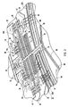
- the sensor 10 includes a sensing element formed on a supporting wafer or substrate 12 generally shown in FIG. 1 and more specifically shown in FIGS. 8-34 .
- the substrate 12 is made of silicon, according to one embodiment, and has a bottom layer 100 and has an insulation layer 102 and epitaxial layer 104 formed on top as shown in FIG. 34 .
- the sensing element includes a ring 14 that is generally supported by a plurality of springs 16 each having first and second spring members (portions) that extend from a center hub or post 18 to support the ring 14 relative to the supporting substrate 12.
- the ring 14 is circular, however, other shaped rings may be employed according to other embodiments.
- the ring 14, springs 16 and central post 18 may also be made of silicon to form an all-silicon monolithic structure.
- An all-silicon monolithic structure is disclosed in U.S. Patent No. 5,547,093 , which is hereby incorporated herein by reference.
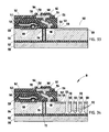
- the ring 14 is shown surrounded by a number of electrode structures 20 formed on the substrate 12 and spaced at 45° intervals.
- the electrode structures 20 form an equiangularly spaced electrode pattern in close proximity to the perimeter of the ring 14.
- the ring 14 and the electrodes 20 are formed of an electrically conductive material, particularly silicon, enabling the ring 14 to form a capacitor with complimentary features, referred to as capacitive plates, when a voltage potential is present.
- Electrodes structures 20 are configured as drive electrodes 20A that drive the ring 14 into resonance when energized, while other electrode structures 20 are configured as sensing electrodes 20B to capacitively sense the proximity of the vibration pattern of the ring 14, which will vary due to Coriolis forces that occur when the sensor 10 is subjected to rotary motion about an axis perpendicular to the substrate 12.
- Each of the electrode structures 20 are also configured to include balance electrodes 20C which, when energized, match the resonant peaks of the natural flexural modes of the ring 14 by inducing electrical spring softening in the ring 14 and in the springs 16, making the device responsive to Coriolis forces that occur when the sensor 10 is subjected to rotary motion about an axis perpendicular to the substrate 12.
- the balance electrodes 20C are formed by at least one pair of moving capacitive plates interdigitated with fixed plates and shown being radially inward from the drive and sensing electrodes 20A and 20B, and are electrically interconnected to electrical conductors 22. Additional balance electrodes 24 are shown disposed equiangularly around the perimeter of the ring 14, which serve to fine balance the sensing structure.
- the balance electrodes 24 are offset by 22.5° relative to electrode structures 20 and capacitively coupled to the ring 14 and electrically interconnected with some of the concentric conductors 22.
- the ring 14, springs 16 and central post 18 are electrically insulated from the wafer 12, and electrically interconnected to electrical conductors 22 outside the ring 14 so as to allow an appropriate electrical potential to be established between the moving structure and the electrodes 20A, 20B, 20C and 24.
- the motion sensor 10 is configured to detect angular velocity about the vertical axis of the ring 14, and therefore rotary movement about an axis of a body, such as an automobile, to which the sensor 10 is mounted.
- conditioning circuitry (not shown) is formed on and electrically interconnects with the sensing electrodes 20B, and differential driving and sensing techniques may be employed.
- One example of a motion sensor having suitable conditioning circuitry and employing differential driving and sensing techniques is disclosed in U.S. Patent No. 5,872,313 , the entire disclosure of which is hereby incorporated herein by reference. The operational requirements of conditioning circuitry and the driving and sensing techniques should be appreciated by those skilled in the art, and therefore are not discussed herein in detail.
- Performance of the sensor 10 may be optimized by equiangularly positioning the electrode structures 20 around the perimeter of the ring 14. It should be appreciated that at least one drive electrode is required, and that more preferably at least two drive electrodes 20A are employed, with the two drive electrodes 20A offset from each other by about 45°, according to one embodiment. However, other electrode configurations are foreseeable. It should also be appreciated that at least one sensing electrode 20B is employed, and that more preferably a plurality of sensing electrodes 20B are employed. Further, the performance of the sensor 10 may be enhanced by increasing the number of sensing electrodes 20B present. According to one embodiment, it should be further appreciated that at least one balance electrode 20C is employed, and that more preferable a plurality of balancing electrodes 20C are employed.
- the electrode structures 20 are shown in FIG. 3 generally employing a base plate or trunk 30 that extends radially from the ring 14, and multiple pairs of opposing teeth or plates 32 extending perpendicularly from the trunk 30. Because the trunk 30 and the plates 32 are physically connected to the ring 14 and formed integrally with the ring 14, the trunk 30 and plates 32 are subjected to the same vibratory movement as the ring 14. A stop may be employed for limiting the lateral movement from the trunk 30, and therefore prevents the plates 32 from contacting the surrounding electrode structure due to excessive angular and/or linear acceleration of the ring 14.
- the trunk 30 and plates 32 may be subjected to thermal expansion and contraction with the ring 14 when subjected to variations in temperatures, which may be compensated for according to known techniques, such as is disclosed in U.S. Patent No. 5,872,313 . It should be appreciated that temperature compensation is generally not needed with the disclosed embodiment of the sensor 10 due to the all silicon construction.
- Each electrode structure 20 further includes an arrangement of fixed electrodes 34 that are interdigitized with the movable plates 32.
- the fixed capacitive plates 34 are fixed to the support substrate 12.
- Four of the electrode structures 20 employ the outermost pairs of movable capacitive plates to form drive electrodes and the pair of radially inward movable capacitive plates 32 form balance electrodes, whereas the other four electrode structures 20 employ the outermost pair of movable capacitive plates 32 to form sensing electrodes and employ the innermost pair of movable capacitive plates 32 to form balance electrodes 20C.
- the movable capacitive plates 32 are movable relative to the fixed capacitive plates 34 such that the distance therebetween changes the capacitive coupling.
- CMOS integrated circuits Due to the significant differences in the electrical performance of CMOS transistors realized in a ⁇ 111> plane or other planes compared to the performance of CMOS transistors realized in ⁇ 100> or ⁇ 110> planes, almost all CMOS integrated circuits (ICs) utilize silicon substrate orientations of ⁇ 100> or ⁇ 110>.
- C 11 ⁇ ⁇ C 11 ⁇ cos 4 ⁇ ⁇ + sin 4 ⁇ ⁇ + 2 ⁇ C 12 + C 14 cos 2 ⁇ ⁇ ⁇ sin 2 ⁇ ⁇
- C 11 is the longitudinal modulus of elasticity along the ⁇ 100> direction
- C 12 and C 44 are the corresponding transverse moduli of elasticity.
- C 11 1.66
- C 12 0.639
- C 44 0.796. It should be noted that C 11 ⁇ ⁇ has a larger value at 45°, 135°, 225° and 315° angles than at right angle locations of 0°, 90°, 180° and 270°.
- the ring 14 is configured with a substantially uniform width.
- the ring 14 may be configured with a varying width, such as shown in FIG. 2A .
- the width of the ring 14 varies according to a sinusoidal waveform to provide maximum ring widths 14A at 0°, 90°, 180°, and 270°, and to provide minimum ring widths 14B at 45°, 135°, 225°, and 315°.
- the mass compensator ring 14 accounts for varying modulus of elasticity around the ring 14.
- the ring angular rate sensor 10 operates on the principle of Coriolis force.
- the sensor 10 measures angular velocity by monitoring the position of nodes in its two-node flexural vibration pattern. There are two degenerate frequencies of equal values associated with the two-node flexural mode.
- the ring is electrostatically driven into an elliptical-shape vibration, at least one location (primary) on the ring, the motion at this primary location is radial by nature. However, the radial motion at the 45° (secondary) locations from the primary location is ideally zero and only tangential motions exist at these locations.
- the vibration pattern which has four nodes and four anti-nodes at eight locations on the ring 14 tends to precess, resulting in energy coupling from the primary locations to the secondary locations, resulting in radial motion at the secondary locations.
- the coupling efficiency strongly depends on matching the frequencies of the two-node flexural degenerate frequencies. Assuming matched primary and secondary mode frequencies, the amplitude of the radial motion at secondary locations due to node precession because of the applied Coriolis force is proportional to the amplitude of the angular rate input. Any difference in the frequency of the degenerate modes will reduce the energy coupling from the primary mode to the secondary mode, and thus reduce the sensitivity of the device to angular rate input.
- the angular rate sensor 10 operates based on mode matching of its two flexural modes and symmetric damping.
- the mode numbers of the angular rate sensor 10 are a function of ring material properties, ring dimension and the design and dimension of the supporting springs 16.
- the two-node flexural modes have been discovered through ANSYS simulations to be the fourth and fifth modes of the rate sensor 10, according to one embodiment.
- the fourth and fifth two-node flexural mode matching is employed to sense angular velocity, based on vibration coupling through the Coriolis force. In the absence of angular rate inputs, the ring vibrates and causes forced oscillation on the 0° and 90° locations.
- the oscillation may be achieved using a known phase locked loop (PLL) circuit using the ring 14 as a reference frequency input and a voltage controlled oscillator (VCO) whose frequency is locked to the ring frequency.
- PLL phase locked loop
- VCO voltage controlled oscillator
- the primary mode generally all the amplitude of ring vibration is in the first normal mode (0° and 90° locations), which is referred to as the primary mode, and there is no radial motion in the second mode ( ⁇ 45° locations) which is referred to as the secondary mode.
- the Coriolis force Upon experiencing rotation, the Coriolis force will cause energy to be transferred from the primary mode to the secondary mode, building up vibration amplitude in the secondary mode.
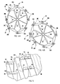
- FIG. 4A An exaggerated version of the two-node flexural motion of the ring angular rate sensor 10 is illustrated in FIG. 4A in the primary mode vibration and is shown in FIG. 4B in the secondary mode vibration.
- the motion sensor 10 advantageously employs a spring design that provides insensitivity to the silicon crystal orientation modulus of elasticity variation.
- the motion sensor 10 employs sixteen springs 16 (eight pairs) that are attached to the ring 14 at 45° increment angular locations at one end and to the fixed anchor center post 18 at the other end.
- each of the eight pairs of springs 16 is constructed with two straight beams, namely B1 and B2. It should also be noted that beams B1 and B2 are oriented at ⁇ 22.5° with respect to X- and Y-axes, respectively. This strategic beam positioning assures that all segments contributing to the construction of each of the eight pairs of springs 16 have constant modulus of elasticity, which simply ensures a matched spring constant for all springs 16.
- the second cause of mismatch between the two-node flexural mode frequencies is the varying modulus of elasticity around the ring 14.
- the variation of the modulus of elasticity around the ring 14 follows the aforementioned equation, which implies that the modulus of elasticity is matched at locations of 0°, 90°, 180° and 270°.
- the modulus of elasticity is also matched at locations of 45°, 135°, 225° and 315°.
- the modulus of elasticity exhibits a minimum value at 0°, 90°, 180° and 270° locations and maximum value at 45°, 135°, 225° and 315° locations.
- the primary and secondary frequencies matching of the two-node flexural mode is determined by the matching of the spring constant amongst the springs 16 and the matching of the spring constant at 0° and 45° locations on the ring 14.
- the width of the ring 14 may be varied according to the above equation as shown in FIG. 2A or by employing lumped compensating masses 50 at the inward end of trunk 30 at each of the 45°, 135°, 225° and 315° locations, as shown in FIGS. 1 and 3 . Due to the designed-in structure symmetries and matching of the modulus of elasticity within the ring 14 and the springs 16, symmetric damping is assured. Symmetric damping assures minimum sensor error due to drive amplitudes or temperature. This is advantageous for proper device performance in practical settings.
- the senor 10 is described particularly as an angular rate motion sensor, those skilled in the art will appreciate that the sensor 10 could also operate as an acceleration sensor, or as a position sensor. Further, four, six and eight node operation of the sensor 10 is possible. The separation of the resonant peaks between the four, six and eight node resonant frequencies in the disclosed embodiment is very wide for the sensor 10; by nearly a factor of two. This allows for easy discrimination between the resonant frequencies.
- the sensor components both movable and fixed, including the ring 14, springs 16, highly compliant external tethers 22, compensating masses 50, interdigitated members including capacitor plates 32 and 34, support structures and anchors may be formed from a silicon-on-insulator (SOI) substrate along with on-board electronic compensating circuitry.
- SOI silicon-on-insulator
- the sensor components are all made of single crystal silicon, and therefore generally have no thermal mismatch that would need compensation.
- the sensor components are fabricated in the plane of the substrate, which makes them less prone to damage than components of conventional devices.
- the sensor components are also formed and released during the same photolithographic and etch steps, thereby decreasing the process complexity, and lowering the costs of manufacture.
- the electrical contact to the ring 14 is made with highly compliant external tethers 22 that form electrical connections.
- the tethers 22 eliminate the need for contact to the center hub 18 of the sensor 10, and the known problems associated with a center hub contact, such as wire bonding damage, stray capacitances, and variable capacitances from wire bonds moving relative to each other.
- All of the sensor components are anchored to, but cantilevered from, an insulator film (oxide 102) on top of an underlying substrate 100 as shown in FIG. 34 , which is achieved through center hub 18, and/or through the highly compliant external tethers 22. All sensor components are otherwise free to move, according to one embodiment. This arrangement with trench isolation provides for electrically and mechanically isolated components.
- a trench isolation scheme is utilized to form one or more trenches 112 to isolate portions of the epi layer 104 shown in FIG. 34 , as well as the sensor components.
- Isolation trenches 112 may be provided as shown in FIG. 5 and may be lined with an insulator film, such as an oxide, filled with an appropriate material such as polysilicon 118, and then capped so that conductors can carry electrical signals across the isolation areas. Later, other trenches 170, such as those surrounding a delineated sensor component like the ring 14 or a compliant tether 22 are formed. The ends 40 of the filled isolation trenches 112 protrude into the trenches 170 isolating the moving element 22A as shown in FIG. 5 .
- the ends 40 of the filled isolation trenches 112 then act as anti-stiction bumps, thus preventing the lateral stiction of the movable sensor components, such as the ring 14 and the highly compliant external tethers 22, and other sensor components, to the walls of the epi layer, and the fixed sensor components surrounding them.
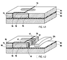
- the components of the sensor 10 both movable and fixed, may be perforated to provide openings that allow for relatively low mass, yet still retaining appropriate rigidity, and to aid in the manufacture of the sensor 10. In some designs, a lower mass for certain sensor components is desirable. Further, to aid in the manufacture of several of the sensor components, perforations may be desirable. Sensor components such as the ring 14, trunk 30 and compensating masses 50 may all be perforated as shown in FIGS. 6 and 7 . In addition, other sensor components, such as tethers 22 and 22A and capacitive plates 32 may include perforations 80.
- corners of several sensor components may be compensated to include portions of the epi layer 104, as shown by reference identifier 52 in FIG. 7 .
- the corner compensation 52 allows for process variation during the delineation and release processes.
- the movable capacitive drive and sense electrodes are connected to trunk 30 whose attachment to the ring 14 is cantilevered from the ring 14.
- the cantilevered connection has two attachment points to the ring 14 for stability, and to allow a perforation 80 between the ring 14 and the trunk 30.
- the perforation 80 may further aid the manufacture of the sensor.
- Differential drive and differential sense further improve the sensor vibration rejection and the temperature response.
- the angular rate sensor 10, according to the present invention may advantageously be employed on a vehicle, such as a wheeled automobile.
- the angular rate sensor 10 may be employed in an electronics stability control system to prevent accidents caused by unwanted angular rotations of a moving vehicle. In doing so, the angular rate sensor 10 is used to detect the unwanted angular rotations.
- a method of making an all-silicon integrated sensor 10 on silicon-on-insulator (SOI) substrate will now be described.
- the method is discussed in connection with making an all-silicon angular rate sensor, such as sensor 10 described herein.
- the method may be employed to manufacture other silicon sensor devices. These devices may be made simultaneously on the same substrate and in any combination.
- the method employs a CMOS process, modified to include an isolation and anti-stiction bump module, a defect getter module, and a sensor delineation etch and release module.
- the CMOS circuitry provides on-board signal processing for the fabricated sensor 10.
- the isolation process module provides isolation between regions of the device silicon layer, between the sensor element and the compensating electronics, and between components of the sensor element. Additionally, the isolation process module provides anti-stiction bumps such that the ring and other moveable portions of the sensor element, such as the external tethers, do not stick to portions of the surrounding sensor.
- the method of making the sensor is flexible, such that sensors made with the process may sense different physical quantities, such as angular rate, angular acceleration, and linear acceleration in one or more than one direction. These devices may be made simultaneously, alone or in any advantageous combination.
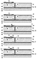
- the process method begins with a starting material having a silicon substrate 100 on the bottom with an oxide insulation layer 102 provided on top, and an epitaxial (epi) device layer 104 of silicon formed upon the layer of oxide 102.
- the device layer 104 has a thickness of approximately 40 micrometers, and the layer of oxide 102 has a thickness in the range of 100 angstroms to 2 micrometers.
- the starting material including the underlying substrate 100, the oxide insulation layer 102, and the epitaxial (epi) device layer 104 are illustrated in FIG. 8 according to one embodiment.
- an oxide layer 110 is provided on top of the silicon device layer 104, and mask and etching steps open portions of the oxide layer 110.
- a second thinner layer of oxide 111 is then formed in the window in the first oxide 110 on the silicon device layer 104, creating recess 106.
- An n-type dopant 108 such as phosphorus, is then implanted through the second oxide film 111, but not through the first oxide film 110, into the silicon (N-well implant) device layer 104, and the silicon is then annealed and the dopant activated, such as by heating.
- the surface of the silicon device layer 104 is then stripped of oxide layers 110 and 111.
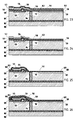
- another oxide film 113 is then formed on the top surface of the silicon device layer 104.
- the oxide film 113 is masked and etched, and then the same mask is used to etch one or more high aspect ratio trenches 112 through the silicon device layer 104 to the buried oxide layer 102 of the silicon substrate 100 as shown in FIG. 10 .
- the trenches 112 in the silicon device layer are lined with a dielectric layer 114, such as an oxide, as shown in FIG. 11 , and the trenches 112 are thereafter filled completely with a conformal material 118, such as polysilicon or nitride, as shown in FIG. 12 .
- the conformal material 118 is removed from the top surface of the structure, leaving the high aspect ratio trenches 112 filled with the conformal material 118 as shown in FIG. 13 .
- the oxide 113 on the top surface of the silicon device layer 104 is then removed, leaving the liner oxide 114 and the conformal material 118 in the planarized trenches 112.
- the trenches 112 provide electrical isolation between different portions of the epitaxial device layer 104.
- Yet another oxide film 116 is formed upon the top surface of the device, including upon the planarized top surfaces of the one or more trenches 112 as shown in FIG. 14 .
- a mask is patterned on the surface, and a p-type dopant 120, such as boron, is implanted into the silicon 104 through the oxide 116 in the open windows areas of the mask.
- an inorganic film 122 such as nitride, is then formed on the surface as shown in FIG. 15 .
- a mask is patterned and the inorganic film 122 is etched in the windows 124 to expose the oxide 116 in selected areas. The mask is then stripped.
- a mask may be patterned and a p-type dopant, such as boron (not shown), may be implanted into the substrate through the oxide in the open windows in the mask.
- This p-type dopant may serve as a field implant to adjust resistivity of the surface where circuitry is to be formed.
- the mask is then stripped.
- a mask may then be patterned and a p-type dopant, such as BF2 or argon (not shown), may be implanted into the substrate through the open windows in the mask.
- a p-type dopant such as BF2 or argon (not shown) may be implanted into the substrate through the open windows in the mask.
- This additional p-type dopant may serve as a getter for collecting impurities, particularly away from electronics.
- the mask is then stripped.
- an additional thickness of oxide 128 is then selectively formed in those areas of the substrate not covered by the inorganic film 122.
- An etch is done to remove any oxide 128 that was formed upon the inorganic film layer 122, but leaves the most recently formed additional thickness of oxide largely intact.
- the inorganic film 122 is then removed from the surface in the step shown in FIG. 18 . This leaves the surface covered with two thicknesses of oxide 128 and 116, each thickness in different areas of the substrate surface.
- An oxide etch is then performed to remove the thinner of the two oxide films 116, exposing the silicon in those areas, and leaving most of the thicker oxide intact.
- the steps shown in FIGS. 17 , 18 and 19 may be implemented using processes collectively known as a LOCOS process.
- an oxide film 132 is then formed upon the exposed silicon regions of the substrate. Little additional oxide forms on the areas of the substrate covered by the thicker oxide film 128.
- a p-type dopant such as boron (not shown), is then implanted through the thinner oxide film 132 into the silicon 104. This p-type dopant adjusts the surface dopant concentrations in select regions.
- the thicker oxide layer 128 blocks the dopant from entering the silicon in those regions.
- the thin oxide film 132 is then etched away to expose the silicon in those regions.
- an oxide film 133 is then formed upon the exposed silicon regions of the substrate. Then a layer of polysilicon 134 is deposited upon the surface. An n-type dopant, such as phosphorus (not shown), is then introduced into the polysilicon and is thermally activated. This n-type dopant dopes the polysilicon 134 to create enhanced conductivity of the polysilicon.
- n-type dopant such as phosphorus (not shown) is then introduced into the polysilicon and is thermally activated. This n-type dopant dopes the polysilicon 134 to create enhanced conductivity of the polysilicon.
- a mask is patterned and portions of the polysilicon film 134 are etched to expose the oxide in selected areas as shown in FIG. 21 .
- the mask is then stripped. Exposed portions of oxide film 133 are then removed.
- An oxide film 138 is then formed upon the surface, including on the polysilicon. Little additional oxide forms on the areas of the substrate covered by the thicker oxide film 128.
- An inorganic film 140 such as nitride, is then formed on the surface as shown in FIG. 22 .
- a layer of polysilicon 143 is deposited upon the surface as shown in FIG. 23 .
- An n-type dopant such as phosphorus (not shown), is then introduced into the polysilicon.
- the n-type dopant creates an n-type polysilicon with enhanced conductivity.
- a dielectric blocking film 144 such as undoped silicon glass (USG) or boron phosphorus silicon glass (BPSG), is then deposited on the polysilicon, and is densified/annealed.
- a mask is patterned and a portion of the blocking film 144 is etched through the open windows in the mask to expose portions of the polysilicon layer.
- An n-type dopant such as phosphorus (not shown), is then introduced into the exposed areas of polysilicon, and is activated. This creates a polysilicon resistor circuit component.
- the blocking film 144 is then removed as shown in FIG. 24 .
- a mask is patterned and portions of the polysilicon film 143 and nitride film 140 are etched to expose the oxide 128 and 138 in selected areas. The mask is then stripped. An oxide film 145 is then formed upon the surface of the polysilicon 143. Little additional oxide forms on the areas of the substrate covered by the thicker oxide film.
- a mask is patterned and a p-type dopant, such as boron (not shown), is introduced into selected regions of the substrate.
- a p-type dopant such as boron (not shown)
- the mask is then stripped.
- the boron p-type dopant creates a circuit element, such as a resistor according to one example.
- a mask is then patterned and a first n-type dopant, such as arsenic (not shown), is introduced into selected regions of the substrate.
- a second n-type dopant such as phosphorus (not shown), is introduced into the same selected regions of the substrate.
- the mask is then stripped, and the dopants are thermally activated. This step forms one of the source or drain areas of a transistor device (e.g., CMOS).
- a mask is patterned and a p-type dopant, such as BF2 (not shown), is introduced into selected regions of the substrate. The mask is then stripped. The p-type dopant forms the other of the source or drain of the transistor device.
- An inorganic film 149 such as a deposited oxide, is then formed upon the surface as shown in FIG. 25 . The dopant is then thermally activated.
- An inorganic film 150 such as a spin-on glass and/or an oxide film, is formed upon the surface of oxide 149 as shown in FIG. 26 . A thermal treatment is then performed.
- a mask is patterned, and the inorganic film 149 and oxide film 138 and inorganic film 150 are etched in selected regions 152 to expose the silicon 104. This forms contact regions 152.
- the same patterned etching can be used to form contact regions on the polysilicon regions 143 and 134 to create electrical circuit pathways.
- a first metal film 154 is then formed on the substrate and within region 152 to make conductive contact with silicon 104.
- a mask is then patterned and selected areas of the first metal film 154 are etched to achieve the desired conductivity path as shown in FIG. 28 .
- a first inorganic film such as a deposited oxide
- a second inorganic film such as a spin-on glass
- the surface is then etched to form a largely planar surface, and then a third inorganic film, such as a deposited oxide, is formed on the surface.
- the three aforementioned inorganic films are identified together as composite oxide layer 156 in FIG. 29 and serve to provide a planar dielectric surface between conductive elements.
- a chemical mechanical planarization (CMP) process may be employed to planarize the wafer surface after all metal and inter-level metal dielectric film sequences.
- a mask is then patterned and portions of the composite oxide 156 covering the first metal 154 are etched to form one or more via openings 158 as shown in FIG. 30 .
- a second metal film 160 is then formed on the surface and in contact with the first metal 154 to fill in the via openings.
- a mask is patterned and selected areas of the second metal 160 are etched.
- the mask is stripped, and an inorganic film 162, such as an oxynitride, is formed on the surface.
- a mask is then applied to the device side (front) surface of the substrate, and the various films, including inorganics like oxide, nitride, oxynitride, and polysilicon, are removed from the back surface of the substrate, resulting in a bare silicon back surface.
- the mask is then stripped.
- a mask is then patterned and portions 166 of the inorganic film 162 covering the second metal 160 are etched to form exposed contact pads.
- the mask is then stripped.
- a thermal treatment is then applied to anneal the metal.
- a mask is patterned and portions of the inorganic layers 138, 149, 150 and 156 covering the silicon are then etched to expose the silicon in the regions where the sensing elements are formed.
- the etch may comprise isotropic or anisotropic etch methods.
- the mask is then stripped.
- a mask is then patterned and portions of the silicon are anisotropically etched, such as by a DRIE etch tool, to delineate and release the sensor elements as shown in FIG. 34 .
- the mask is then stripped, which completes the device fabrication.
- a previously made cap wafer may be aligned to the device wafer, and the two wafers bonded together to provide a cap over the sensor element.
- the cap provides for a hermetic seal of the sensor element, thus protecting it from physical damage due to handling, particulate contamination, and moisture, etc.
- the bond may entail using a glass frit.
- the frit may be used over the on-board circuitry of the integrated sensor without affecting the functionality of the circuit.
- Micromachined sensor elements formed by this process may be fabricated in the plane of the substrate. This makes them significantly less prone to damage than conventional approaches which have sensor components formed above the plane of the substrate.
- the process is versatile in that sensors may be made with the process that sense different physical quantities, such as angular rate, angular acceleration, and linear acceleration in one or more than one direction. These devices may be formed simultaneously on the same substrate in any advantageous combination.
- the process is simple, and does not require buried cavities, thus preventing the process complexities, process difficulties, and yield losses associated with such processes.
- the sensor element release process is simple, and may be done in the same equipment as the sensor delineation process. It does not require additional expensive capital equipment or difficult processes at the release step. No liquid or vapor undercuts are required and thus, no stiction results from wet undercut processes.
- the sensor element is delineated using a DRIE trench etch, and then is released using a DRIE lateral etch. The lateral etch may be done as a footer etch in a DRIE machine.
- the getter implant module getters defects in the device layer according to one embodiment, thus increasing the CMOS yield.
- the process may not include a getter implant module.
- the bottom of the epi device layer 104 may be implanted with an appropriate getter implant prior to bonding the device layer 104 onto the insulating layer 102 on the substrate 100.
- the isolation process module provides anti-stiction bumps for lateral stiction prevention for moving structures such as rings and fingers.
- Other isolation and anti-stiction bumps may be formed during the sensor element delineation and release process.
- a method of forming isolation and anti-stiction bumps according to an isolation process according to another embodiment is further illustrated in FIGS. 35-42 .
- a method of forming anti-stiction bumps generally includes providing a starting material having a silicon substrate 100 on the bottom with an oxide insulation layer 102 provided on top, and an epitaxial device layer 104 of silicon formed upon the layer of oxide 102. Additionally, an oxide film 113 is formed on top of the silicon device layer 104.
- trenches 112 are formed in a desired shape extending through silicon device layer 104 and oxide layer 113. The trenches 112 are formed extending down to the top surface of the oxide insulation layer 102.
- the side walls of trenches 112 in the silicon device layer are lined with a dielectric layer 114, such as an oxide, as shown in FIG. 37 .
- the next step in the process of forming the anti-stiction bumps includes filling the trenches 112 with a conformal material 118, such as polysilicon or nitride.
- the conformal material 118 on top of oxide layer 113 is then removed, leaving conformal material 118 in the trenches 112 as shown in FIG. 39 .
- the oxide 113 on the top surface of the silicon device layer 104 is then removed, leaving the liner oxide 114 and the conformal material 118 in the planarized trenches 112.
- the trenches 112 provide electrical isolation between different portions of the epitaxial device layer 104.
- An oxide film 116 is then formed upon the top surface of the device, including upon the planarized top surfaces of the one or more trenches 112 as seen in FIG. 40 .
- the sensor device is shown following the step of removing the oxide film 116 about a portion of the sensor device so as to expose part of the trenches.
- the epitaxial device layer is etched away so as to form a suspended member 22A and to provide for the trench having conformal isolation and anti-stiction members extending therefrom, labeled 40.
- the extending member 40 extending from trench 112 forms one or more isolation and anti-stiction bumps.
- the anti-stiction bumps 40 provide for lateral stiction prevent for moving structures, such as structure 22A.
- the electrical isolation of portions of the device silicon layer may be moved to the end of the process.
- the frit bonding may occur over the on-board electronics of the integrated sensor device without adversely affecting the functionality of the circuitry.
Abstract
Description
- The present invention generally relates to sensors, and more particularly relates to a silicon motion sensor, such as an angular rate sensor, and a method of manufacturing a sensor.
- Motion sensors, such as angular rate sensors, are commonly employed in various applications to sense motion, such as angular rate. Sensors such as these are commonly manufactured as microelectromechanical system (MEMS) devices using conventional micromachining techniques. Typically, a MEMS sensor may employ an electrically conductive micromachined plate of metal or silicon as a sensing element. Examples of such devices are disclosed in
U.S. Patent Nos. 5,450,751 ;5,547,093 and5,872,313 . - Sensors of the type described above are capable of extremely precise measurements. However, conventional sensors may suffer various drawbacks which may include mismatches in the resonant frequency between primary and secondary flexure nodes at the sensor element, and may suffer from relatively high mass and performance limitations. Another drawback of some conventional sensors is undesirable sensitivity to vibration. Therefore, it would be desirable to provide for a motion sensor and method of manufacturing a sensor that overcomes drawbacks of the prior art.
EP-A-1120630 discloses a sensor in accordance with the preamble of Claim 1.US-B-6276205 discloses a method of fabricating a sensor. - In accordance with one aspect of the present invention, a motion sensor is provided. The motion sensor includes a support substrate and a silicon sensing ring formed within and supported by the substrate and having a flexural resonance. The motion sensor also includes at least one drive electrode including drive capacitive plates for applying electrostatic force on the ring to cause the ring to resonate, and at least one sense electrode including sense capacitor plates for sensing a change in capacitance indicative of the vibration nodes of resonance of the ring so as to sense motion. The motion sensor further includes a plurality of silicon support springs connecting the substrate to the ring, wherein the support springs are located at an angle to substantially match a modulus of elasticity of the silicon support springs. According to a further aspect of the present invention, the support springs include a first spring located at an angle in the range of 20° to 25° with respect to the crystalline orientation of the silicon, and a second spring oriented at an angle in the range of 65° to 70° with respect to the crystalline orientation of the silicon.
- According to another aspect of the present invention, a method of making a silicon integrated sensor on an SOI substrate is provided. The method includes the step of providing a substrate having an insulation layer on a top surface, and providing a silicon epitaxial layer on top of the insulation layer. The method also includes the steps of forming a first trench extending through the epitaxial layer and reaching the insulation layer so as to isolate a first portion of the epitaxial layer from a second portion of the epitaxial layer, and disposing a fill material within the first trench. The method also includes the steps of forming one or more electrical components on the first portion of the epitaxial layer, and forming one or more contacts on the second portion of the epitaxial layer. The method further includes the step of forming one or more second trenches in the second portion of the epitaxial layer so as to provide one or more moving elements within the second portion of the epitaxial layer, wherein the one or more movable elements serve as sensing elements. According to a further embodiment, the method includes the step of forming one or more anti-stiction bumps to prevent a portion of a moving element from sticking to an adjacent feature of the sensor.
- These and other features, advantages and objects of the present invention will be further understood and appreciated by those skilled in the art by reference to the following specification, claims and appended drawings.
- The present invention will now be described, by way of example, with reference to the accompanying drawings, in which:
-
FIG. 1 is a top view of a micromachined angular rate motion sensor according to one embodiment of the present invention; -
FIG. 2 is an enlarged view of section 11-11 ofFIG. 1 illustrating the springs connecting the ring to the substrate, according to one embodiment; -
FIG. 2A is a schematic diagram illustrating a ring having a varying width according to another embodiment; -
FIG. 3 is an enlarged perspective view of section III-III ofFIG. 1 further illustrating the electrode structure; -
FIGS. 4A and 4B are schematic diagrams illustrating a two-node flexural motion of the ring angular rate sensor in respective primary mode vibration and secondary mode vibration; -
FIG. 5 is an enlarged perspective view of section V taken fromFIG. 3 further illustrating isolation protrusions that form anti-stiction bumps, according to one embodiment; -
FIG. 6 is an enlarged perspective sectional view of the motion sensor further illustrating a perforated structure according to another embodiment; -
FIG. 7 is an enlarged perspective sectional view of the motion sensor further illustrating a perforated compensation mass and corner compensations, according to a further embodiment; -
FIG. 8 is a cross-sectional view of a sensor device being manufactured following the initial steps, according to one embodiment of the present invention; -
FIG. 9 is a cross-sectional view of the sensor device illustrating another step of the method; -
FIG. 10 is a cross-sectional view of the device illustrating another step of the method; - F1G. 11 is a cross-sectional view of the device illustrating another step of the method;
-
FIG. 12 is a cross-sectional view of the device illustrating another step of the method; -
FIG. 13 is a cross-sectional view of the device illustrating another step of the method; -
FIG. 14 is a cross-sectional view of the device illustrating another step of the method; -
FIG. 15 is a cross-sectional view of the device illustrating another step of the method; -
FIG. 16 is a cross-sectional view of the device illustrating another step of the method; -
FIG. 17 is a cross-sectional view of the device illustrating another step of the method; -
FIG. 18 is a cross-sectional view of the device illustrating another step of the method; -
FIG. 19 is a cross-sectional view of the device illustrating another step of the method; -
FIG. 20 is a cross-sectional view of the device illustrating another step of the method; -
FIG. 21 is a cross-sectional view of the device illustrating another step of the method; -
FIG. 22 is a cross-sectional view of the device illustrating another step of the method; -
FIG. 23 is a cross-sectional view of the device illustrating another step of the method; -
FIG. 24 is a cross-sectional view of the device illustrating another step of the method; -
FIG. 25 is a cross-sectional view of the device illustrating another step of the method; -
FIG. 26 is a cross-sectional view of the device illustrating another step of the method; -
FIG. 27 is a cross-sectional view of the device illustrating another step of the method; -
FIG. 28 is a cross-sectional view of the device illustrating another step of the method; -
FIG. 29 is a cross-sectional view of the device illustrating another step of the method; - F1G. 30 is a cross-sectional view of the device illustrating another step of the method;
-
FIG. 31 is a cross-sectional view of the device illustrating another step of the method; -
FIG. 32 is a cross-sectional view of the device illustrating another step of the method; -
FIG. 33 is a cross-sectional view of the device illustrating another step of the method; -
FIG. 34 is a cross-sectional view of the sensor device according to a further step of the method; -
FIG. 35 is a perspective cross-sectional view of a sensor device showing an initial step of forming anti-stiction bumps according to one embodiment of an isolation formation process; -
FIG. 36 is a perspective cross-sectional view of the sensor device ofFIG. 35 illustrating another step in the method of forming anti-stiction bumps; -
FIG. 37 is a perspective cross-sectional view of the sensor device ofFIG. 36 further illustrating another step in the method of forming anti-stiction bumps; -
FIG. 38 is a perspective cross-sectional view of the sensor device ofFIG. 37 further illustrating another step in the method of forming anti-stiction bumps; -
FIG. 39 is a perspective cross-sectional view of the sensor device ofFIG. 38 further illustrating another step in the method of forming anti-stiction bumps; -
FIG. 40 is a perspective cross-sectional view of the sensor device ofFIG. 39 further illustrating another step in the method of forming anti-stiction bumps; -
FIG. 41 is a perspective cross-sectional view of the sensor device ofFIG. 40 further illustrating another step in the method of forming anti-stiction bumps; and -
FIG. 42 is a perspective cross-sectional view of the sensor device ofFIG. 41 further illustrating a further step in the method of forming anti-stiction bumps. - Referring to
FIGS. 1-3 , amotion sensor 10 is generally illustrated according to a first embodiment of the present invention. Themotion sensor 10 shown and described herein in the disclosed embodiment is an angular rate motion sensor for sensing angular rate. However, it should be appreciated by those skilled in the art that thesensor 10 could also be configured to operate to sense other motions, such as angular acceleration, and may further be configured to sense angular position according to other embodiments. - As seen in
FIG. 1 , thesensor 10 includes a sensing element formed on a supporting wafer orsubstrate 12 generally shown inFIG. 1 and more specifically shown inFIGS. 8-34 . Thesubstrate 12 is made of silicon, according to one embodiment, and has abottom layer 100 and has aninsulation layer 102 andepitaxial layer 104 formed on top as shown inFIG. 34 . The sensing element includes aring 14 that is generally supported by a plurality ofsprings 16 each having first and second spring members (portions) that extend from a center hub or post 18 to support thering 14 relative to the supportingsubstrate 12. In the disclosed embodiment, thering 14 is circular, however, other shaped rings may be employed according to other embodiments. Thering 14, springs 16 andcentral post 18 may also be made of silicon to form an all-silicon monolithic structure. One example of an all-silicon monolithic structure is disclosed inU.S. Patent No. 5,547,093 , which is hereby incorporated herein by reference. - The
ring 14 is shown surrounded by a number ofelectrode structures 20 formed on thesubstrate 12 and spaced at 45° intervals. Theelectrode structures 20 form an equiangularly spaced electrode pattern in close proximity to the perimeter of thering 14. Thering 14 and theelectrodes 20 are formed of an electrically conductive material, particularly silicon, enabling thering 14 to form a capacitor with complimentary features, referred to as capacitive plates, when a voltage potential is present. Some of theelectrode structures 20 are configured asdrive electrodes 20A that drive thering 14 into resonance when energized, whileother electrode structures 20 are configured as sensingelectrodes 20B to capacitively sense the proximity of the vibration pattern of thering 14, which will vary due to Coriolis forces that occur when thesensor 10 is subjected to rotary motion about an axis perpendicular to thesubstrate 12. - Each of the
electrode structures 20 are also configured to includebalance electrodes 20C which, when energized, match the resonant peaks of the natural flexural modes of thering 14 by inducing electrical spring softening in thering 14 and in thesprings 16, making the device responsive to Coriolis forces that occur when thesensor 10 is subjected to rotary motion about an axis perpendicular to thesubstrate 12. Thebalance electrodes 20C are formed by at least one pair of moving capacitive plates interdigitated with fixed plates and shown being radially inward from the drive andsensing electrodes electrical conductors 22.Additional balance electrodes 24 are shown disposed equiangularly around the perimeter of thering 14, which serve to fine balance the sensing structure. Thebalance electrodes 24 are offset by 22.5° relative to electrodestructures 20 and capacitively coupled to thering 14 and electrically interconnected with some of theconcentric conductors 22. Thering 14, springs 16 andcentral post 18 are electrically insulated from thewafer 12, and electrically interconnected toelectrical conductors 22 outside thering 14 so as to allow an appropriate electrical potential to be established between the moving structure and theelectrodes - The
motion sensor 10 is configured to detect angular velocity about the vertical axis of thering 14, and therefore rotary movement about an axis of a body, such as an automobile, to which thesensor 10 is mounted. In one embodiment, conditioning circuitry (not shown) is formed on and electrically interconnects with thesensing electrodes 20B, and differential driving and sensing techniques may be employed. One example of a motion sensor having suitable conditioning circuitry and employing differential driving and sensing techniques is disclosed inU.S. Patent No. 5,872,313 , the entire disclosure of which is hereby incorporated herein by reference. The operational requirements of conditioning circuitry and the driving and sensing techniques should be appreciated by those skilled in the art, and therefore are not discussed herein in detail. - Performance of the
sensor 10 may be optimized by equiangularly positioning theelectrode structures 20 around the perimeter of thering 14. It should be appreciated that at least one drive electrode is required, and that more preferably at least twodrive electrodes 20A are employed, with the twodrive electrodes 20A offset from each other by about 45°, according to one embodiment. However, other electrode configurations are foreseeable. It should also be appreciated that at least onesensing electrode 20B is employed, and that more preferably a plurality ofsensing electrodes 20B are employed. Further, the performance of thesensor 10 may be enhanced by increasing the number ofsensing electrodes 20B present. According to one embodiment, it should be further appreciated that at least onebalance electrode 20C is employed, and that more preferable a plurality of balancingelectrodes 20C are employed. - The
electrode structures 20 are shown inFIG. 3 generally employing a base plate ortrunk 30 that extends radially from thering 14, and multiple pairs of opposing teeth orplates 32 extending perpendicularly from thetrunk 30. Because thetrunk 30 and theplates 32 are physically connected to thering 14 and formed integrally with thering 14, thetrunk 30 andplates 32 are subjected to the same vibratory movement as thering 14. A stop may be employed for limiting the lateral movement from thetrunk 30, and therefore prevents theplates 32 from contacting the surrounding electrode structure due to excessive angular and/or linear acceleration of thering 14. Thetrunk 30 andplates 32 may be subjected to thermal expansion and contraction with thering 14 when subjected to variations in temperatures, which may be compensated for according to known techniques, such as is disclosed inU.S. Patent No. 5,872,313 . It should be appreciated that temperature compensation is generally not needed with the disclosed embodiment of thesensor 10 due to the all silicon construction. - Each
electrode structure 20 further includes an arrangement of fixedelectrodes 34 that are interdigitized with themovable plates 32. The fixedcapacitive plates 34 are fixed to thesupport substrate 12. Four of theelectrode structures 20 employ the outermost pairs of movable capacitive plates to form drive electrodes and the pair of radially inwardmovable capacitive plates 32 form balance electrodes, whereas the other fourelectrode structures 20 employ the outermost pair ofmovable capacitive plates 32 to form sensing electrodes and employ the innermost pair ofmovable capacitive plates 32 to formbalance electrodes 20C. Themovable capacitive plates 32 are movable relative to the fixedcapacitive plates 34 such that the distance therebetween changes the capacitive coupling. Changes in capacitive coupling between the movable sensing plates and fixed plates are detected and indicative of the sensed angular rate. With the application of Coriolis force, radial flexural motion at nodes indicates angular rate sensed by thesensor 10, while flexural motion at anti-nodes indicates motion of the ring. - The design of the ring
angular rate sensor 10 in silicon as a mechanical structure poses challenges when the crystal plane orientation is <100> or <110>. Integrated microsensors incorporate microsensing structure(s) along with its associated drive, sense, control and calibration electronic circuits on the same piece of silicon substrate to realize a high performance system on chip at competitive cost. Due to the significant differences in the electrical performance of CMOS transistors realized in a <111> plane or other planes compared to the performance of CMOS transistors realized in <100> or <110> planes, almost all CMOS integrated circuits (ICs) utilize silicon substrate orientations of <100> or <110>. - It is known that certain mechanical properties of single crystal silicon are also orientation dependent and also vary with dopant type and dopant concentration. It turns out that the modulus of elasticity of single crystal silicon is also orientation dependent. The longitudinal modulus of elasticity


where C11 is the longitudinal modulus of elasticity along the <100> direction, and C12 and C44 are the corresponding transverse moduli of elasticity. For intrinsic silicon, C11 = 1.66, C12 = 0.639, and C44 = 0.796. It should be noted that
- According to one embodiment shown in
FIGS. 1 and3 , thering 14 is configured with a substantially uniform width. According to another embodiment, thering 14 may be configured with a varying width, such as shown inFIG. 2A . In this embodiment, the width of thering 14 varies according to a sinusoidal waveform to providemaximum ring widths 14A at 0°, 90°, 180°, and 270°, and to provideminimum ring widths 14B at 45°, 135°, 225°, and 315°. By varying the width based on a sinusoidal waveform, themass compensator ring 14 accounts for varying modulus of elasticity around thering 14. - The ring
angular rate sensor 10 operates on the principle of Coriolis force. Thesensor 10 measures angular velocity by monitoring the position of nodes in its two-node flexural vibration pattern. There are two degenerate frequencies of equal values associated with the two-node flexural mode. When the ring is electrostatically driven into an elliptical-shape vibration, at least one location (primary) on the ring, the motion at this primary location is radial by nature. However, the radial motion at the 45° (secondary) locations from the primary location is ideally zero and only tangential motions exist at these locations. Upon the application of angular rate input, the vibration pattern which has four nodes and four anti-nodes at eight locations on thering 14 tends to precess, resulting in energy coupling from the primary locations to the secondary locations, resulting in radial motion at the secondary locations. The coupling efficiency strongly depends on matching the frequencies of the two-node flexural degenerate frequencies. Assuming matched primary and secondary mode frequencies, the amplitude of the radial motion at secondary locations due to node precession because of the applied Coriolis force is proportional to the amplitude of the angular rate input. Any difference in the frequency of the degenerate modes will reduce the energy coupling from the primary mode to the secondary mode, and thus reduce the sensitivity of the device to angular rate input. - The
angular rate sensor 10 operates based on mode matching of its two flexural modes and symmetric damping. The mode numbers of theangular rate sensor 10 are a function of ring material properties, ring dimension and the design and dimension of the supporting springs 16. The two-node flexural modes have been discovered through ANSYS simulations to be the fourth and fifth modes of therate sensor 10, according to one embodiment. The fourth and fifth two-node flexural mode matching is employed to sense angular velocity, based on vibration coupling through the Coriolis force. In the absence of angular rate inputs, the ring vibrates and causes forced oscillation on the 0° and 90° locations. The oscillation may be achieved using a known phase locked loop (PLL) circuit using thering 14 as a reference frequency input and a voltage controlled oscillator (VCO) whose frequency is locked to the ring frequency. In this situation, generally all the amplitude of ring vibration is in the first normal mode (0° and 90° locations), which is referred to as the primary mode, and there is no radial motion in the second mode (± 45° locations) which is referred to as the secondary mode. Upon experiencing rotation, the Coriolis force will cause energy to be transferred from the primary mode to the secondary mode, building up vibration amplitude in the secondary mode. The ratio of the amplitude of the secondary mode vibration to the amplitude of the primary mode vibration may be representative of the following equation:
where α is the ring angular gain, Q is the quality factor, ω is the two-node flexural natural frequency, and the Ω is the angular velocity experienced by thesensor 10. - An exaggerated version of the two-node flexural motion of the ring
angular rate sensor 10 is illustrated inFIG. 4A in the primary mode vibration and is shown inFIG. 4B in the secondary mode vibration. It has been discovered that the use of curved or semi-circular springs in prior art devices may result in a gross frequency mismatch between the primary and secondary two-node flexural normal modes, rendering the conventional device generally insensitive to angular velocity input. This is at least partly due to the fact that the modulus of elasticity of single crystal silicon is orientation dependent. Themotion sensor 10 according to the present invention advantageously employs a spring design that provides insensitivity to the silicon crystal orientation modulus of elasticity variation. Specifically, in one embodiment themotion sensor 10 employs sixteen springs 16 (eight pairs) that are attached to thering 14 at 45° increment angular locations at one end and to the fixedanchor center post 18 at the other end. - The
springs 16 are illustrated in the layout of thesensor 10 inFIGS. 1 and2 . As discussed with regard to the above equation, the modulus of elasticity of silicon is equal along 0°, 90°, 180° and 270° directions. The modulus of elasticity of <100> and <110> silicon is also equal along ± 22.5° and ± 67.5° with respect to 0° and 90° directions in <100> and <110> silicon. With particular reference toFIG. 2 , each of the eight pairs ofsprings 16 is constructed with two straight beams, namely B1 and B2. It should also be noted that beams B1 and B2 are oriented at ± 22.5° with respect to X- and Y-axes, respectively. This strategic beam positioning assures that all segments contributing to the construction of each of the eight pairs ofsprings 16 have constant modulus of elasticity, which simply ensures a matched spring constant for all springs 16. - The second cause of mismatch between the two-node flexural mode frequencies is the varying modulus of elasticity around the
ring 14. The variation of the modulus of elasticity around thering 14 follows the aforementioned equation, which implies that the modulus of elasticity is matched at locations of 0°, 90°, 180° and 270°. The modulus of elasticity is also matched at locations of 45°, 135°, 225° and 315°. However, it should be noted that the modulus of elasticity exhibits a minimum value at 0°, 90°, 180° and 270° locations and maximum value at 45°, 135°, 225° and 315° locations. The primary and secondary frequencies matching of the two-node flexural mode is determined by the matching of the spring constant amongst thesprings 16 and the matching of the spring constant at 0° and 45° locations on thering 14. In order to compensate for the spring constant variation around thering 14, the width of thering 14 may be varied according to the above equation as shown inFIG. 2A or by employing lumped compensatingmasses 50 at the inward end oftrunk 30 at each of the 45°, 135°, 225° and 315° locations, as shown inFIGS. 1 and3 . Due to the designed-in structure symmetries and matching of the modulus of elasticity within thering 14 and thesprings 16, symmetric damping is assured. Symmetric damping assures minimum sensor error due to drive amplitudes or temperature. This is advantageous for proper device performance in practical settings. - While the
sensor 10 is described particularly as an angular rate motion sensor, those skilled in the art will appreciate that thesensor 10 could also operate as an acceleration sensor, or as a position sensor. Further, four, six and eight node operation of thesensor 10 is possible. The separation of the resonant peaks between the four, six and eight node resonant frequencies in the disclosed embodiment is very wide for thesensor 10; by nearly a factor of two. This allows for easy discrimination between the resonant frequencies. - The sensor components, both movable and fixed, including the
ring 14, springs 16, highly compliantexternal tethers 22, compensatingmasses 50, interdigitated members includingcapacitor plates - The electrical contact to the
ring 14 is made with highly compliantexternal tethers 22 that form electrical connections. Thetethers 22 eliminate the need for contact to thecenter hub 18 of thesensor 10, and the known problems associated with a center hub contact, such as wire bonding damage, stray capacitances, and variable capacitances from wire bonds moving relative to each other. All of the sensor components are anchored to, but cantilevered from, an insulator film (oxide 102) on top of anunderlying substrate 100 as shown inFIG. 34 , which is achieved throughcenter hub 18, and/or through the highly compliantexternal tethers 22. All sensor components are otherwise free to move, according to one embodiment. This arrangement with trench isolation provides for electrically and mechanically isolated components. - In one embodiment, a trench isolation scheme is utilized to form one or
more trenches 112 to isolate portions of theepi layer 104 shown inFIG. 34 , as well as the sensor components.Isolation trenches 112 may be provided as shown inFIG. 5 and may be lined with an insulator film, such as an oxide, filled with an appropriate material such aspolysilicon 118, and then capped so that conductors can carry electrical signals across the isolation areas. Later,other trenches 170, such as those surrounding a delineated sensor component like thering 14 or acompliant tether 22 are formed. The ends 40 of the filledisolation trenches 112 protrude into thetrenches 170 isolating the movingelement 22A as shown inFIG. 5 . The ends 40 of the filledisolation trenches 112 then act as anti-stiction bumps, thus preventing the lateral stiction of the movable sensor components, such as thering 14 and the highly compliantexternal tethers 22, and other sensor components, to the walls of the epi layer, and the fixed sensor components surrounding them. - In addition, the components of the
sensor 10, both movable and fixed, may be perforated to provide openings that allow for relatively low mass, yet still retaining appropriate rigidity, and to aid in the manufacture of thesensor 10. In some designs, a lower mass for certain sensor components is desirable. Further, to aid in the manufacture of several of the sensor components, perforations may be desirable. Sensor components such as thering 14,trunk 30 and compensatingmasses 50 may all be perforated as shown inFIGS. 6 and 7 . In addition, other sensor components, such astethers capacitive plates 32 may includeperforations 80. - In one embodiment of the
motion sensor 10, corners of several sensor components may be compensated to include portions of theepi layer 104, as shown byreference identifier 52 inFIG. 7 . Thecorner compensation 52 allows for process variation during the delineation and release processes.
In one embodiment, the movable capacitive drive and sense electrodes are connected totrunk 30 whose attachment to thering 14 is cantilevered from thering 14. The cantilevered connection has two attachment points to thering 14 for stability, and to allow aperforation 80 between thering 14 and thetrunk 30. Theperforation 80 may further aid the manufacture of the sensor. Differential drive and differential sense further improve the sensor vibration rejection and the temperature response. - It should be appreciated that the
angular rate sensor 10, according to the present invention may advantageously be employed on a vehicle, such as a wheeled automobile. For example, theangular rate sensor 10 may be employed in an electronics stability control system to prevent accidents caused by unwanted angular rotations of a moving vehicle. In doing so, theangular rate sensor 10 is used to detect the unwanted angular rotations. - A method of making an all-silicon integrated
sensor 10 on silicon-on-insulator (SOI) substrate, will now be described. The method is discussed in connection with making an all-silicon angular rate sensor, such assensor 10 described herein. However, it should be appreciated that the method may be employed to manufacture other silicon sensor devices. These devices may be made simultaneously on the same substrate and in any combination. - According to one embodiment, the method employs a CMOS process, modified to include an isolation and anti-stiction bump module, a defect getter module, and a sensor delineation etch and release module. The CMOS circuitry provides on-board signal processing for the fabricated
sensor 10. The isolation process module provides isolation between regions of the device silicon layer, between the sensor element and the compensating electronics, and between components of the sensor element. Additionally, the isolation process module provides anti-stiction bumps such that the ring and other moveable portions of the sensor element, such as the external tethers, do not stick to portions of the surrounding sensor. The method of making the sensor is flexible, such that sensors made with the process may sense different physical quantities, such as angular rate, angular acceleration, and linear acceleration in one or more than one direction. These devices may be made simultaneously, alone or in any advantageous combination. - The method will now be described in connection with the series of processing steps, which in one embodiment are shown in the drawing
FIGS. 8-34 . It should be appreciated that some common processing steps are not shown or described in detail herein. The process method according to one embodiment of the present invention begins with a starting material having asilicon substrate 100 on the bottom with anoxide insulation layer 102 provided on top, and an epitaxial (epi)device layer 104 of silicon formed upon the layer ofoxide 102. According to one example, thedevice layer 104 has a thickness of approximately 40 micrometers, and the layer ofoxide 102 has a thickness in the range of 100 angstroms to 2 micrometers. The starting material including theunderlying substrate 100, theoxide insulation layer 102, and the epitaxial (epi)device layer 104 are illustrated inFIG. 8 according to one embodiment. - In the step shown in
FIG. 9 , anoxide layer 110 is provided on top of thesilicon device layer 104, and mask and etching steps open portions of theoxide layer 110. A second thinner layer ofoxide 111 is then formed in the window in thefirst oxide 110 on thesilicon device layer 104, creatingrecess 106. An n-type dopant 108, such as phosphorus, is then implanted through thesecond oxide film 111, but not through thefirst oxide film 110, into the silicon (N-well implant)device layer 104, and the silicon is then annealed and the dopant activated, such as by heating. The surface of thesilicon device layer 104 is then stripped ofoxide layers - In the steps of
FIG. 10 , anotheroxide film 113 is then formed on the top surface of thesilicon device layer 104. Theoxide film 113 is masked and etched, and then the same mask is used to etch one or more highaspect ratio trenches 112 through thesilicon device layer 104 to the buriedoxide layer 102 of thesilicon substrate 100 as shown inFIG. 10 . Thetrenches 112 in the silicon device layer are lined with adielectric layer 114, such as an oxide, as shown inFIG. 11 , and thetrenches 112 are thereafter filled completely with aconformal material 118, such as polysilicon or nitride, as shown inFIG. 12 . Theconformal material 118 is removed from the top surface of the structure, leaving the highaspect ratio trenches 112 filled with theconformal material 118 as shown inFIG. 13 . This substantially planarizes the top surface of thesilicon device layer 104, and completes the formation of the anti-stiction bumps 40 shown inFIG. 5 . Theoxide 113 on the top surface of thesilicon device layer 104 is then removed, leaving theliner oxide 114 and theconformal material 118 in theplanarized trenches 112. Thetrenches 112 provide electrical isolation between different portions of theepitaxial device layer 104. - Yet another
oxide film 116 is formed upon the top surface of the device, including upon the planarized top surfaces of the one ormore trenches 112 as shown inFIG. 14 . A mask is patterned on the surface, and a p-type dopant 120, such as boron, is implanted into thesilicon 104 through theoxide 116 in the open windows areas of the mask. After the mask is stripped, aninorganic film 122, such as nitride, is then formed on the surface as shown inFIG. 15 . - Referring next to
FIG. 16 , a mask is patterned and theinorganic film 122 is etched in thewindows 124 to expose theoxide 116 in selected areas. The mask is then stripped. - In another step, a mask may be patterned and a p-type dopant, such as boron (not shown), may be implanted into the substrate through the oxide in the open windows in the mask. This p-type dopant may serve as a field implant to adjust resistivity of the surface where circuitry is to be formed. The mask is then stripped.
- A mask may then be patterned and a p-type dopant, such as BF2 or argon (not shown), may be implanted into the substrate through the open windows in the mask. This additional p-type dopant may serve as a getter for collecting impurities, particularly away from electronics. The mask is then stripped.
- Referring to
FIG. 17 , an additional thickness ofoxide 128 is then selectively formed in those areas of the substrate not covered by theinorganic film 122. An etch is done to remove anyoxide 128 that was formed upon theinorganic film layer 122, but leaves the most recently formed additional thickness of oxide largely intact. Theinorganic film 122 is then removed from the surface in the step shown inFIG. 18 . This leaves the surface covered with two thicknesses ofoxide oxide films 116, exposing the silicon in those areas, and leaving most of the thicker oxide intact. The steps shown inFIGS. 17 ,18 and 19 may be implemented using processes collectively known as a LOCOS process. - Referring to
FIG. 19 , anoxide film 132 is then formed upon the exposed silicon regions of the substrate. Little additional oxide forms on the areas of the substrate covered by thethicker oxide film 128. A p-type dopant, such as boron (not shown), is then implanted through thethinner oxide film 132 into thesilicon 104. This p-type dopant adjusts the surface dopant concentrations in select regions. Thethicker oxide layer 128 blocks the dopant from entering the silicon in those regions. Thethin oxide film 132 is then etched away to expose the silicon in those regions. - In
FIG. 20 , anoxide film 133 is then formed upon the exposed silicon regions of the substrate. Then a layer ofpolysilicon 134 is deposited upon the surface. An n-type dopant, such as phosphorus (not shown), is then introduced into the polysilicon and is thermally activated. This n-type dopant dopes thepolysilicon 134 to create enhanced conductivity of the polysilicon. - A mask is patterned and portions of the
polysilicon film 134 are etched to expose the oxide in selected areas as shown inFIG. 21 . The mask is then stripped. Exposed portions ofoxide film 133 are then removed. Anoxide film 138 is then formed upon the surface, including on the polysilicon. Little additional oxide forms on the areas of the substrate covered by thethicker oxide film 128. Aninorganic film 140, such as nitride, is then formed on the surface as shown inFIG. 22 . Then a layer ofpolysilicon 143 is deposited upon the surface as shown inFIG. 23 . An n-type dopant, such as phosphorus (not shown), is then introduced into the polysilicon. The n-type dopant creates an n-type polysilicon with enhanced conductivity. Adielectric blocking film 144, such as undoped silicon glass (USG) or boron phosphorus silicon glass (BPSG), is then deposited on the polysilicon, and is densified/annealed. - A mask is patterned and a portion of the blocking
film 144 is etched through the open windows in the mask to expose portions of the polysilicon layer. An n-type dopant, such as phosphorus (not shown), is then introduced into the exposed areas of polysilicon, and is activated. This creates a polysilicon resistor circuit component. The blockingfilm 144 is then removed as shown inFIG. 24 . - Referring to
FIG. 25 , a mask is patterned and portions of thepolysilicon film 143 andnitride film 140 are etched to expose theoxide oxide film 145 is then formed upon the surface of thepolysilicon 143. Little additional oxide forms on the areas of the substrate covered by the thicker oxide film. - A mask is patterned and a p-type dopant, such as boron (not shown), is introduced into selected regions of the substrate. The mask is then stripped. The boron p-type dopant creates a circuit element, such as a resistor according to one example.
- A mask is then patterned and a first n-type dopant, such as arsenic (not shown), is introduced into selected regions of the substrate. A second n-type dopant, such as phosphorus (not shown), is introduced into the same selected regions of the substrate. The mask is then stripped, and the dopants are thermally activated. This step forms one of the source or drain areas of a transistor device (e.g., CMOS).
- A mask is patterned and a p-type dopant, such as BF2 (not shown), is introduced into selected regions of the substrate. The mask is then stripped. The p-type dopant forms the other of the source or drain of the transistor device. An
inorganic film 149, such as a deposited oxide, is then formed upon the surface as shown inFIG. 25 . The dopant is then thermally activated. Aninorganic film 150, such as a spin-on glass and/or an oxide film, is formed upon the surface ofoxide 149 as shown inFIG. 26 . A thermal treatment is then performed. - Referring to
FIG. 27 , a mask is patterned, and theinorganic film 149 andoxide film 138 andinorganic film 150 are etched in selectedregions 152 to expose thesilicon 104. This formscontact regions 152. The same patterned etching can be used to form contact regions on thepolysilicon regions - Referring to
FIG. 28 , afirst metal film 154 is then formed on the substrate and withinregion 152 to make conductive contact withsilicon 104. A mask is then patterned and selected areas of thefirst metal film 154 are etched to achieve the desired conductivity path as shown inFIG. 28 . - A first inorganic film, such as a deposited oxide, is then formed on the surface. A second inorganic film, such as a spin-on glass, is then formed on the surface. The surface is then etched to form a largely planar surface, and then a third inorganic film, such as a deposited oxide, is formed on the surface. The three aforementioned inorganic films are identified together as
composite oxide layer 156 inFIG. 29 and serve to provide a planar dielectric surface between conductive elements. According to other embodiments, a chemical mechanical planarization (CMP) process may be employed to planarize the wafer surface after all metal and inter-level metal dielectric film sequences. - A mask is then patterned and portions of the
composite oxide 156 covering thefirst metal 154 are etched to form one or more viaopenings 158 as shown inFIG. 30 . - Referring to
FIG. 31 , asecond metal film 160 is then formed on the surface and in contact with thefirst metal 154 to fill in the via openings. A mask is patterned and selected areas of thesecond metal 160 are etched. The mask is stripped, and aninorganic film 162, such as an oxynitride, is formed on the surface. - A mask is then applied to the device side (front) surface of the substrate, and the various films, including inorganics like oxide, nitride, oxynitride, and polysilicon, are removed from the back surface of the substrate, resulting in a bare silicon back surface. The mask is then stripped.
- Referring to
FIG. 32 , a mask is then patterned andportions 166 of theinorganic film 162 covering thesecond metal 160 are etched to form exposed contact pads. The mask is then stripped. A thermal treatment is then applied to anneal the metal. - Referring to
FIG. 33 , a mask is patterned and portions of theinorganic layers - A mask is then patterned and portions of the silicon are anisotropically etched, such as by a DRIE etch tool, to delineate and release the sensor elements as shown in
FIG. 34 . This includes formingtrenches 170 which provide physical and electrical isolation and/or releases sensor element(s) 172. Both vertical and lateral etching may be employed. The mask is then stripped, which completes the device fabrication. - A previously made cap wafer (not shown) may be aligned to the device wafer, and the two wafers bonded together to provide a cap over the sensor element. The cap provides for a hermetic seal of the sensor element, thus protecting it from physical damage due to handling, particulate contamination, and moisture, etc. The bond may entail using a glass frit. The frit may be used over the on-board circuitry of the integrated sensor without affecting the functionality of the circuit.
- Finally, in steps after the integrated sensor is completed and capped, the bond pads are exposed, the device is tested, and the die are singulated.
- Micromachined sensor elements formed by this process may be fabricated in the plane of the substrate. This makes them significantly less prone to damage than conventional approaches which have sensor components formed above the plane of the substrate.
- The process is versatile in that sensors may be made with the process that sense different physical quantities, such as angular rate, angular acceleration, and linear acceleration in one or more than one direction. These devices may be formed simultaneously on the same substrate in any advantageous combination. The process is simple, and does not require buried cavities, thus preventing the process complexities, process difficulties, and yield losses associated with such processes.
- The sensor element release process is simple, and may be done in the same equipment as the sensor delineation process. It does not require additional expensive capital equipment or difficult processes at the release step. No liquid or vapor undercuts are required and thus, no stiction results from wet undercut processes. In one embodiment, the sensor element is delineated using a DRIE trench etch, and then is released using a DRIE lateral etch. The lateral etch may be done as a footer etch in a DRIE machine.
- The getter implant module getters defects in the device layer according to one embodiment, thus increasing the CMOS yield. According to other embodiments, the process may not include a getter implant module. According to a further embodiment, the bottom of the
epi device layer 104 may be implanted with an appropriate getter implant prior to bonding thedevice layer 104 onto the insulatinglayer 102 on thesubstrate 100. - The isolation process module provides anti-stiction bumps for lateral stiction prevention for moving structures such as rings and fingers. Other isolation and anti-stiction bumps may be formed during the sensor element delineation and release process. A method of forming isolation and anti-stiction bumps according to an isolation process according to another embodiment is further illustrated in
FIGS. 35-42 . - Referring to
FIG. 35 , a method of forming anti-stiction bumps generally includes providing a starting material having asilicon substrate 100 on the bottom with anoxide insulation layer 102 provided on top, and anepitaxial device layer 104 of silicon formed upon the layer ofoxide 102. Additionally, anoxide film 113 is formed on top of thesilicon device layer 104. Next, in the step illustrated inFIG. 36 ,trenches 112 are formed in a desired shape extending throughsilicon device layer 104 andoxide layer 113. Thetrenches 112 are formed extending down to the top surface of theoxide insulation layer 102. - The side walls of
trenches 112 in the silicon device layer are lined with adielectric layer 114, such as an oxide, as shown inFIG. 37 . - Referring to
FIG. 38 , the next step in the process of forming the anti-stiction bumps includes filling thetrenches 112 with aconformal material 118, such as polysilicon or nitride. Theconformal material 118 on top ofoxide layer 113 is then removed, leavingconformal material 118 in thetrenches 112 as shown inFIG. 39 . Theoxide 113 on the top surface of thesilicon device layer 104 is then removed, leaving theliner oxide 114 and theconformal material 118 in theplanarized trenches 112. Thetrenches 112 provide electrical isolation between different portions of theepitaxial device layer 104. Anoxide film 116 is then formed upon the top surface of the device, including upon the planarized top surfaces of the one ormore trenches 112 as seen inFIG. 40 . - Referring to
FIG. 41 , the sensor device is shown following the step of removing theoxide film 116 about a portion of the sensor device so as to expose part of the trenches. Next, inFIG. 42 the epitaxial device layer is etched away so as to form a suspendedmember 22A and to provide for the trench having conformal isolation and anti-stiction members extending therefrom, labeled 40. The extendingmember 40 extending fromtrench 112 forms one or more isolation and anti-stiction bumps. The anti-stiction bumps 40 provide for lateral stiction prevent for moving structures, such asstructure 22A. - Sensors made from the process have no need for temperature compensation since all the mechanical components of the senor element, including the drive, sense, and balance electrodes, the ring, springs, etc., are made of single crystal silicon. Thus, no differences exist in thermal expansion rates of the sensor element members.
- The electrical isolation of portions of the device silicon layer may be moved to the end of the process. The frit bonding may occur over the on-board electronics of the integrated sensor device without adversely affecting the functionality of the circuitry.
Claims (14)
- A motion sensor (10) comprising:a support substrate (12);a silicon sensing ring (14) formed within and supported by the substrate and having a flexural resonance;at least one drive electrode (20A) comprising drive capacitive plates for applying electrostatic force on the ring (14) to cause the ring (14) to resonate; andat least one sense electrode (20B) comprising sense capacitive plates for sensing a change in capacitance indicative of the vibration nodes of resonance of the ring (14) so as to sense motion; characterised bya plurality of silicon support springs (16) connecting the substrate (12) to the ring (14), wherein the support springs (16) are located at an angle to substantially match a modulus of elasticity of the silicon support springs (16); andan electrical connection comprising at least one external tether in contact with the ring (14).
- The sensor as defined in claim 1 further comprising at least one balance electrode (20C) comprising balance capacitive plates for applying electrostatic force to the ring (14) to balance vibratory motion of the resonance of the ring.
- The sensor of claim 1, wherein the sensor (10) is capable of at least four node operation.
- The sensor as defined in claim 1, wherein the support springs (16) comprise a first spring portion (B1) located at an angle in the range of 20° to 25° with respect to crystalline orientation of the silicon, and a second spring portion (B2) oriented at an angle in the range of 65° to 70° with respect to the crystalline orientation of the silicon.
- The sensor as defined in claim 4, wherein the first spring portion (B1) is oriented at an angle of approximately 22.5° and the second spring portion (B2) is oriented at an angle of approximately 67.5° from the X and Y-axes of the sensor.
- The sensor as defined in claim 1, wherein the motion sensor (10) comprises an angular rate sensor, or wherein the motion sensor (10) comprises an angular acceleration sensor, or wherein the motion sensor (10) comprises an angular position sensor.
- The sensor as defined in claim 1, wherein the substrate (12) is comprised of silicon (100), or wherein the substrate (12) is comprised of silicon-on-insulator.
- The sensor as defined in claim 1 further comprising a compensation mass (50) provided on the ring (14) to compensate for a modulus of elasticity variation around the ring (14).
- The sensor as defined in claim 8, wherein the compensation mass (50) is located at locations at approximately 45° from the X and Y-axes of the sensor, or wherein the compensation mass (50) is located at locations at approximately 45° with respect to the crystal planes in the substrate (12).
- The sensor as defined in claim 1, wherein the silicon sensing ring (14) has a periodically varying width around its circumference.
- The sensor as defined in claim 1, wherein the springs (16) comprise a first radial portion (B1) and a second portion (B2) so as to have all spring portions located at an angle to substantially match a modulus of elasticity of the silicon and/or wherein the springs (16) comprises at least sixteen springs and/or wherein the springs (16) are formed as pairs of springs.
- The sensor as defined in claim 1, wherein the silicon sensing ring (14), the at least one drive electrode (20A), the at least one sense electrode (20B), the plurality of silicon support springs (16), and the at least one external tether, is formed from and within the substrate.
- The sensor as defined in claim 1, wherein the sensor comprises one or more anti-stiction bumps (40) formed to prevent stiction between a moving component and another component of the sensor.
- The sensor as defined in claim 2, wherein the at least one drive electrode (20A), the at least one sense electrode (20B) and the at least one balance electrode (20C) are cantilevered from the ring (14).
Applications Claiming Priority (1)
| Application Number | Priority Date | Filing Date | Title |
|---|---|---|---|
| US12/011,184 US7908922B2 (en) | 2008-01-24 | 2008-01-24 | Silicon integrated angular rate sensor |
Publications (2)
| Publication Number | Publication Date |
|---|---|
| EP2083246A1 EP2083246A1 (en) | 2009-07-29 |
| EP2083246B1 true EP2083246B1 (en) | 2011-07-06 |
Family
ID=40521715
Family Applications (1)
| Application Number | Title | Priority Date | Filing Date |
|---|---|---|---|
| EP09150251A Active EP2083246B1 (en) | 2008-01-24 | 2009-01-08 | Silicon integrated angular rate sensor |
Country Status (3)
| Country | Link |
|---|---|
| US (1) | US7908922B2 (en) |
| EP (1) | EP2083246B1 (en) |
| AT (1) | ATE515680T1 (en) |
Families Citing this family (80)
| Publication number | Priority date | Publication date | Assignee | Title |
|---|---|---|---|---|
| IL181367A (en) * | 2007-02-15 | 2013-03-24 | Elbit Systems Electro Optics Elop Ltd | Vibratory gyroscopic device for determining angular velocity |
| US9970764B2 (en) * | 2009-08-31 | 2018-05-15 | Georgia Tech Research Corporation | Bulk acoustic wave gyroscope with spoked structure |
| CN106536336B (en) | 2014-05-16 | 2019-04-12 | 迪根特技术公司 | Modularization for carrier chassis shapes node and its application method |
| CA2953815A1 (en) | 2014-07-02 | 2016-01-07 | Divergent Technologies, Inc. | Systems and methods for fabricating joint members |
| US9866200B2 (en) * | 2014-10-22 | 2018-01-09 | Microchip Technology Incorporated | Multiple coil spring MEMS resonator |
| US9923545B2 (en) | 2014-10-22 | 2018-03-20 | Microchip Technology Incorporated | Compound spring MEMS resonators for frequency and timing generation |
| US10746548B2 (en) * | 2014-11-04 | 2020-08-18 | Analog Devices, Inc. | Ring gyroscope structural features |
| GB201514114D0 (en) | 2015-08-11 | 2015-09-23 | Atlantic Inertial Systems Ltd | Angular velocity sensors |
| WO2017214580A1 (en) | 2016-06-09 | 2017-12-14 | Divergent Technologies, Inc. | Systems and methods for arc and node design and manufacture |
| US11155005B2 (en) | 2017-02-10 | 2021-10-26 | Divergent Technologies, Inc. | 3D-printed tooling and methods for producing same |
| US10759090B2 (en) | 2017-02-10 | 2020-09-01 | Divergent Technologies, Inc. | Methods for producing panels using 3D-printed tooling shells |
| US10898968B2 (en) | 2017-04-28 | 2021-01-26 | Divergent Technologies, Inc. | Scatter reduction in additive manufacturing |
| US10703419B2 (en) | 2017-05-19 | 2020-07-07 | Divergent Technologies, Inc. | Apparatus and methods for joining panels |
| US11358337B2 (en) | 2017-05-24 | 2022-06-14 | Divergent Technologies, Inc. | Robotic assembly of transport structures using on-site additive manufacturing |
| US11123973B2 (en) | 2017-06-07 | 2021-09-21 | Divergent Technologies, Inc. | Interconnected deflectable panel and node |
| US10919230B2 (en) | 2017-06-09 | 2021-02-16 | Divergent Technologies, Inc. | Node with co-printed interconnect and methods for producing same |
| US10781846B2 (en) | 2017-06-19 | 2020-09-22 | Divergent Technologies, Inc. | 3-D-printed components including fasteners and methods for producing same |
| US10994876B2 (en) | 2017-06-30 | 2021-05-04 | Divergent Technologies, Inc. | Automated wrapping of components in transport structures |
| US11022375B2 (en) | 2017-07-06 | 2021-06-01 | Divergent Technologies, Inc. | Apparatus and methods for additively manufacturing microtube heat exchangers |
| US10895315B2 (en) | 2017-07-07 | 2021-01-19 | Divergent Technologies, Inc. | Systems and methods for implementing node to node connections in mechanized assemblies |
| US10751800B2 (en) | 2017-07-25 | 2020-08-25 | Divergent Technologies, Inc. | Methods and apparatus for additively manufactured exoskeleton-based transport structures |
| US10940609B2 (en) | 2017-07-25 | 2021-03-09 | Divergent Technologies, Inc. | Methods and apparatus for additively manufactured endoskeleton-based transport structures |
| US10605285B2 (en) | 2017-08-08 | 2020-03-31 | Divergent Technologies, Inc. | Systems and methods for joining node and tube structures |
| US10357959B2 (en) | 2017-08-15 | 2019-07-23 | Divergent Technologies, Inc. | Methods and apparatus for additively manufactured identification features |
| US11306751B2 (en) | 2017-08-31 | 2022-04-19 | Divergent Technologies, Inc. | Apparatus and methods for connecting tubes in transport structures |
| US10960611B2 (en) | 2017-09-06 | 2021-03-30 | Divergent Technologies, Inc. | Methods and apparatuses for universal interface between parts in transport structures |
| US11292058B2 (en) | 2017-09-12 | 2022-04-05 | Divergent Technologies, Inc. | Apparatus and methods for optimization of powder removal features in additively manufactured components |
| US10814564B2 (en) | 2017-10-11 | 2020-10-27 | Divergent Technologies, Inc. | Composite material inlay in additively manufactured structures |
| US10668816B2 (en) | 2017-10-11 | 2020-06-02 | Divergent Technologies, Inc. | Solar extended range electric vehicle with panel deployment and emitter tracking |
| US11786971B2 (en) | 2017-11-10 | 2023-10-17 | Divergent Technologies, Inc. | Structures and methods for high volume production of complex structures using interface nodes |
| US10926599B2 (en) | 2017-12-01 | 2021-02-23 | Divergent Technologies, Inc. | Suspension systems using hydraulic dampers |
| US11110514B2 (en) | 2017-12-14 | 2021-09-07 | Divergent Technologies, Inc. | Apparatus and methods for connecting nodes to tubes in transport structures |
| US11085473B2 (en) | 2017-12-22 | 2021-08-10 | Divergent Technologies, Inc. | Methods and apparatus for forming node to panel joints |
| US11534828B2 (en) | 2017-12-27 | 2022-12-27 | Divergent Technologies, Inc. | Assembling structures comprising 3D printed components and standardized components utilizing adhesive circuits |
| US11420262B2 (en) | 2018-01-31 | 2022-08-23 | Divergent Technologies, Inc. | Systems and methods for co-casting of additively manufactured interface nodes |
| US10751934B2 (en) | 2018-02-01 | 2020-08-25 | Divergent Technologies, Inc. | Apparatus and methods for additive manufacturing with variable extruder profiles |
| US11224943B2 (en) | 2018-03-07 | 2022-01-18 | Divergent Technologies, Inc. | Variable beam geometry laser-based powder bed fusion |
| US11267236B2 (en) | 2018-03-16 | 2022-03-08 | Divergent Technologies, Inc. | Single shear joint for node-to-node connections |
| US11254381B2 (en) | 2018-03-19 | 2022-02-22 | Divergent Technologies, Inc. | Manufacturing cell based vehicle manufacturing system and method |
| US11872689B2 (en) | 2018-03-19 | 2024-01-16 | Divergent Technologies, Inc. | End effector features for additively manufactured components |
| US11408216B2 (en) | 2018-03-20 | 2022-08-09 | Divergent Technologies, Inc. | Systems and methods for co-printed or concurrently assembled hinge structures |
| US11613078B2 (en) | 2018-04-20 | 2023-03-28 | Divergent Technologies, Inc. | Apparatus and methods for additively manufacturing adhesive inlet and outlet ports |
| US11214317B2 (en) | 2018-04-24 | 2022-01-04 | Divergent Technologies, Inc. | Systems and methods for joining nodes and other structures |
| US10682821B2 (en) | 2018-05-01 | 2020-06-16 | Divergent Technologies, Inc. | Flexible tooling system and method for manufacturing of composite structures |
| US11020800B2 (en) | 2018-05-01 | 2021-06-01 | Divergent Technologies, Inc. | Apparatus and methods for sealing powder holes in additively manufactured parts |
| US11389816B2 (en) | 2018-05-09 | 2022-07-19 | Divergent Technologies, Inc. | Multi-circuit single port design in additively manufactured node |
| US10691104B2 (en) | 2018-05-16 | 2020-06-23 | Divergent Technologies, Inc. | Additively manufacturing structures for increased spray forming resolution or increased fatigue life |
| US11590727B2 (en) | 2018-05-21 | 2023-02-28 | Divergent Technologies, Inc. | Custom additively manufactured core structures |
| US11441586B2 (en) | 2018-05-25 | 2022-09-13 | Divergent Technologies, Inc. | Apparatus for injecting fluids in node based connections |
| US11035511B2 (en) | 2018-06-05 | 2021-06-15 | Divergent Technologies, Inc. | Quick-change end effector |
| US11292056B2 (en) | 2018-07-06 | 2022-04-05 | Divergent Technologies, Inc. | Cold-spray nozzle |
| US11269311B2 (en) | 2018-07-26 | 2022-03-08 | Divergent Technologies, Inc. | Spray forming structural joints |
| US10836120B2 (en) | 2018-08-27 | 2020-11-17 | Divergent Technologies, Inc . | Hybrid composite structures with integrated 3-D printed elements |
| US11433557B2 (en) | 2018-08-28 | 2022-09-06 | Divergent Technologies, Inc. | Buffer block apparatuses and supporting apparatuses |
| US11826953B2 (en) | 2018-09-12 | 2023-11-28 | Divergent Technologies, Inc. | Surrogate supports in additive manufacturing |
| US11072371B2 (en) | 2018-10-05 | 2021-07-27 | Divergent Technologies, Inc. | Apparatus and methods for additively manufactured structures with augmented energy absorption properties |
| US11260582B2 (en) | 2018-10-16 | 2022-03-01 | Divergent Technologies, Inc. | Methods and apparatus for manufacturing optimized panels and other composite structures |
| US11504912B2 (en) | 2018-11-20 | 2022-11-22 | Divergent Technologies, Inc. | Selective end effector modular attachment device |
| USD911222S1 (en) | 2018-11-21 | 2021-02-23 | Divergent Technologies, Inc. | Vehicle and/or replica |
| US10663110B1 (en) | 2018-12-17 | 2020-05-26 | Divergent Technologies, Inc. | Metrology apparatus to facilitate capture of metrology data |
| US11449021B2 (en) | 2018-12-17 | 2022-09-20 | Divergent Technologies, Inc. | Systems and methods for high accuracy fixtureless assembly |
| US11529741B2 (en) | 2018-12-17 | 2022-12-20 | Divergent Technologies, Inc. | System and method for positioning one or more robotic apparatuses |
| US11885000B2 (en) | 2018-12-21 | 2024-01-30 | Divergent Technologies, Inc. | In situ thermal treatment for PBF systems |
| US11656077B2 (en) | 2019-01-31 | 2023-05-23 | Analog Devices, Inc. | Pseudo-extensional mode MEMS ring gyroscope |
| US11203240B2 (en) | 2019-04-19 | 2021-12-21 | Divergent Technologies, Inc. | Wishbone style control arm assemblies and methods for producing same |
| FR3102240B1 (en) * | 2019-10-18 | 2021-10-01 | Safran Electronics & Defense | Mechanically compensated frequency anisotropy sensor |
| US11912339B2 (en) | 2020-01-10 | 2024-02-27 | Divergent Technologies, Inc. | 3-D printed chassis structure with self-supporting ribs |
| US11590703B2 (en) | 2020-01-24 | 2023-02-28 | Divergent Technologies, Inc. | Infrared radiation sensing and beam control in electron beam additive manufacturing |
| US11479015B2 (en) | 2020-02-14 | 2022-10-25 | Divergent Technologies, Inc. | Custom formed panels for transport structures and methods for assembling same |
| US11884025B2 (en) | 2020-02-14 | 2024-01-30 | Divergent Technologies, Inc. | Three-dimensional printer and methods for assembling parts via integration of additive and conventional manufacturing operations |
| US11535322B2 (en) | 2020-02-25 | 2022-12-27 | Divergent Technologies, Inc. | Omni-positional adhesion device |
| US11421577B2 (en) | 2020-02-25 | 2022-08-23 | Divergent Technologies, Inc. | Exhaust headers with integrated heat shielding and thermal syphoning |
| US11413686B2 (en) | 2020-03-06 | 2022-08-16 | Divergent Technologies, Inc. | Methods and apparatuses for sealing mechanisms for realizing adhesive connections with additively manufactured components |
| US11850804B2 (en) | 2020-07-28 | 2023-12-26 | Divergent Technologies, Inc. | Radiation-enabled retention features for fixtureless assembly of node-based structures |
| US11806941B2 (en) | 2020-08-21 | 2023-11-07 | Divergent Technologies, Inc. | Mechanical part retention features for additively manufactured structures |
| US11872626B2 (en) | 2020-12-24 | 2024-01-16 | Divergent Technologies, Inc. | Systems and methods for floating pin joint design |
| US11947335B2 (en) | 2020-12-30 | 2024-04-02 | Divergent Technologies, Inc. | Multi-component structure optimization for combining 3-D printed and commercially available parts |
| US11928966B2 (en) | 2021-01-13 | 2024-03-12 | Divergent Technologies, Inc. | Virtual railroad |
| EP4304865A1 (en) | 2021-03-09 | 2024-01-17 | Divergent Technologies, Inc. | Rotational additive manufacturing systems and methods |
| US11865617B2 (en) | 2021-08-25 | 2024-01-09 | Divergent Technologies, Inc. | Methods and apparatuses for wide-spectrum consumption of output of atomization processes across multi-process and multi-scale additive manufacturing modalities |
Family Cites Families (24)
| Publication number | Priority date | Publication date | Assignee | Title |
|---|---|---|---|---|
| US4951508A (en) * | 1983-10-31 | 1990-08-28 | General Motors Corporation | Vibratory rotation sensor |
| US5153143A (en) | 1990-02-26 | 1992-10-06 | Delco Electronics Corporation | Method of manufacturing CMOS integrated circuit with EEPROM |
| US5383362A (en) * | 1993-02-01 | 1995-01-24 | General Motors Corporation | Control for vibratory gyroscope |
| US5366916A (en) | 1993-02-04 | 1994-11-22 | Delco Electronics Corporation | Method of making a high voltage implanted channel device for VLSI and ULSI processes |
| US5450751A (en) | 1993-05-04 | 1995-09-19 | General Motors Corporation | Microstructure for vibratory gyroscope |
| US5547093A (en) | 1994-09-14 | 1996-08-20 | Delco Electronics Corporation | Method for forming a micromachine motion sensor |
| US5712427A (en) * | 1995-08-29 | 1998-01-27 | Litton Systems Inc. | Vibratory rotation sensor with scanning-tunneling-transducer readout |
| DE19617666B4 (en) * | 1996-05-03 | 2006-04-20 | Robert Bosch Gmbh | Micromechanical rotation rate sensor |
| US5872313A (en) * | 1997-04-07 | 1999-02-16 | Delco Electronics Corporation | Temperature-compensated surface micromachined angular rate sensor |
| US5872034A (en) | 1997-11-03 | 1999-02-16 | Delco Electronics Corporation | EPROM in double poly high density CMOS |
| GB9817347D0 (en) * | 1998-08-11 | 1998-10-07 | British Aerospace | An angular rate sensor |
| GB9819821D0 (en) | 1998-09-12 | 1998-11-04 | Secr Defence | Improvements relating to micro-machining |
| DE19850066B4 (en) * | 1998-10-30 | 2008-05-21 | Robert Bosch Gmbh | Micromechanical tilt sensor |
| US6128954A (en) * | 1998-12-18 | 2000-10-10 | Delco Electronics Corporation | Spring for a resonance ring of an angular rate sensor |
| US6305222B1 (en) * | 1999-05-27 | 2001-10-23 | Delphi Technologies, Inc. | Road vibration compensated angular rate sensor |
| DE19938206A1 (en) * | 1999-08-12 | 2001-02-15 | Bosch Gmbh Robert | Micro-mechanical rotational acceleration sensor has an oscillating mass fixed at its center with an array of differential measurement capacitors for determination of acceleration directly rather than using time differentiation |
| EP1120630A1 (en) | 2000-01-27 | 2001-08-01 | British Aerospace Public Limited Company | Micromachined angular rate sensor |
| FR2821422B1 (en) | 2001-02-23 | 2003-05-23 | Sagem | PLANAR MECHANICAL RESONATOR SENSITIVE ACCORDING TO AN AXIS PERPENDICULAR TO ITS PLAN |
| GB0122253D0 (en) * | 2001-09-14 | 2001-11-07 | Bae Systems Plc | Vibratory gyroscopic rate sensor |
| US6666092B2 (en) * | 2002-02-28 | 2003-12-23 | Delphi Technologies, Inc. | Angular accelerometer having balanced inertia mass |
| FR2838820B1 (en) | 2002-04-17 | 2006-03-17 | Sagem | METHOD FOR CONSTITUTING A MECHANICAL RESONATOR WITH PLANE MONOLITHIC VIBRATION STRUCTURE MADE IN A CRYSTALLINE MATERIAL, AND RESONATOR SO CONSTITUTED |
| TWI220155B (en) * | 2003-07-25 | 2004-08-11 | Ind Tech Res Inst | Micro vibratory dual-axis sensitive gyroscope |
| DE102004043233B4 (en) | 2003-09-10 | 2014-02-13 | Denso Corporation | A method of manufacturing a movable portion of a semiconductor device |
| US7360423B2 (en) * | 2005-01-29 | 2008-04-22 | Georgia Tech Research Corp. | Resonating star gyroscope |
-
2008
- 2008-01-24 US US12/011,184 patent/US7908922B2/en active Active
-
2009
- 2009-01-08 EP EP09150251A patent/EP2083246B1/en active Active
- 2009-01-08 AT AT09150251T patent/ATE515680T1/en not_active IP Right Cessation
Also Published As
| Publication number | Publication date |
|---|---|
| EP2083246A1 (en) | 2009-07-29 |
| ATE515680T1 (en) | 2011-07-15 |
| US20090188318A1 (en) | 2009-07-30 |
| US7908922B2 (en) | 2011-03-22 |
Similar Documents
| Publication | Publication Date | Title |
|---|---|---|
| EP2083246B1 (en) | Silicon integrated angular rate sensor | |
| US7645627B2 (en) | Method for manufacturing a sensor device | |
| US7270003B2 (en) | BMEMS-type high-sensitivity inertial sensor and manufacturing process thereof | |
| EP1116008B1 (en) | Vibrating gyrometer and its process of fabrication | |
| US6988408B2 (en) | Surface/bulk micromachined single-crystalline silicon micro-gyroscope | |
| US9448069B2 (en) | Microelectromechanical bulk acoustic wave devices and methods | |
| US6845668B2 (en) | Gyroscope | |
| EP1212585B1 (en) | Electrically decoupled micromachined gyroscope | |
| US5535902A (en) | Gimballed vibrating wheel gyroscope | |
| US7637156B2 (en) | Angular velocity sensor with vibrator having ring portion and electrodes positioned inside and outside the ring portion | |
| US6189381B1 (en) | Angular rate sensor made from a structural wafer of single crystal silicon | |
| EP0824702B1 (en) | Gimballed vibrating wheel gyroscope having strain relief features | |
| US7104129B2 (en) | Vertically integrated MEMS structure with electronics in a hermetically sealed cavity | |
| US7581443B2 (en) | Disc resonator gyroscopes | |
| US6792804B2 (en) | Sensor for measuring out-of-plane acceleration | |
| US6761068B1 (en) | Micromechanical rotation rate sensor and method for producing the same | |
| EP1741669B1 (en) | Hidden hinge MEMS device | |
| Song et al. | Wafer level vacuum packaged de-coupled vertical gyroscope by a new fabrication process | |
| US20020017133A1 (en) | Surface/bulk micromachined single-crystalline silicon micro-gyroscope | |
| CN100524614C (en) | Method of manufacturing an electronic device and electronic device |
Legal Events
| Date | Code | Title | Description |
|---|---|---|---|
| PUAI | Public reference made under article 153(3) epc to a published international application that has entered the european phase |
Free format text: ORIGINAL CODE: 0009012 |
|
| AK | Designated contracting states |
Kind code of ref document: A1 Designated state(s): AT BE BG CH CY CZ DE DK EE ES FI FR GB GR HR HU IE IS IT LI LT LU LV MC MK MT NL NO PL PT RO SE SI SK TR |
|
| AX | Request for extension of the european patent |
Extension state: AL BA RS |
|
| 17P | Request for examination filed |
Effective date: 20100129 |
|
| 17Q | First examination report despatched |
Effective date: 20100222 |
|
| AKX | Designation fees paid |
Designated state(s): AT BE BG CH CY CZ DE DK EE ES FI FR GB GR HR HU IE IS IT LI LT LU LV MC MK MT NL NO PL PT RO SE SI SK TR |
|
| GRAP | Despatch of communication of intention to grant a patent |
Free format text: ORIGINAL CODE: EPIDOSNIGR1 |
|
| GRAS | Grant fee paid |
Free format text: ORIGINAL CODE: EPIDOSNIGR3 |
|
| GRAA | (expected) grant |
Free format text: ORIGINAL CODE: 0009210 |
|
| AK | Designated contracting states |
Kind code of ref document: B1 Designated state(s): AT BE BG CH CY CZ DE DK EE ES FI FR GB GR HR HU IE IS IT LI LT LU LV MC MK MT NL NO PL PT RO SE SI SK TR |
|
| REG | Reference to a national code |
Ref country code: GB Ref legal event code: FG4D |
|
| REG | Reference to a national code |
Ref country code: CH Ref legal event code: EP |
|
| REG | Reference to a national code |
Ref country code: IE Ref legal event code: FG4D |
|
| REG | Reference to a national code |
Ref country code: DE Ref legal event code: R096 Ref document number: 602009001709 Country of ref document: DE Effective date: 20110901 |
|
| REG | Reference to a national code |
Ref country code: NL Ref legal event code: VDEP Effective date: 20110706 |
|
| PG25 | Lapsed in a contracting state [announced via postgrant information from national office to epo] |
Ref country code: SI Free format text: LAPSE BECAUSE OF FAILURE TO SUBMIT A TRANSLATION OF THE DESCRIPTION OR TO PAY THE FEE WITHIN THE PRESCRIBED TIME-LIMIT Effective date: 20110706 |
|
| REG | Reference to a national code |
Ref country code: AT Ref legal event code: MK05 Ref document number: 515680 Country of ref document: AT Kind code of ref document: T Effective date: 20110706 |
|
| PG25 | Lapsed in a contracting state [announced via postgrant information from national office to epo] |
Ref country code: NO Free format text: LAPSE BECAUSE OF FAILURE TO SUBMIT A TRANSLATION OF THE DESCRIPTION OR TO PAY THE FEE WITHIN THE PRESCRIBED TIME-LIMIT Effective date: 20111006 Ref country code: FI Free format text: LAPSE BECAUSE OF FAILURE TO SUBMIT A TRANSLATION OF THE DESCRIPTION OR TO PAY THE FEE WITHIN THE PRESCRIBED TIME-LIMIT Effective date: 20110706 Ref country code: NL Free format text: LAPSE BECAUSE OF FAILURE TO SUBMIT A TRANSLATION OF THE DESCRIPTION OR TO PAY THE FEE WITHIN THE PRESCRIBED TIME-LIMIT Effective date: 20110706 Ref country code: SE Free format text: LAPSE BECAUSE OF FAILURE TO SUBMIT A TRANSLATION OF THE DESCRIPTION OR TO PAY THE FEE WITHIN THE PRESCRIBED TIME-LIMIT Effective date: 20110706 Ref country code: BE Free format text: LAPSE BECAUSE OF FAILURE TO SUBMIT A TRANSLATION OF THE DESCRIPTION OR TO PAY THE FEE WITHIN THE PRESCRIBED TIME-LIMIT Effective date: 20110706 Ref country code: PT Free format text: LAPSE BECAUSE OF FAILURE TO SUBMIT A TRANSLATION OF THE DESCRIPTION OR TO PAY THE FEE WITHIN THE PRESCRIBED TIME-LIMIT Effective date: 20111107 Ref country code: LT Free format text: LAPSE BECAUSE OF FAILURE TO SUBMIT A TRANSLATION OF THE DESCRIPTION OR TO PAY THE FEE WITHIN THE PRESCRIBED TIME-LIMIT Effective date: 20110706 Ref country code: HR Free format text: LAPSE BECAUSE OF FAILURE TO SUBMIT A TRANSLATION OF THE DESCRIPTION OR TO PAY THE FEE WITHIN THE PRESCRIBED TIME-LIMIT Effective date: 20110706 Ref country code: IS Free format text: LAPSE BECAUSE OF FAILURE TO SUBMIT A TRANSLATION OF THE DESCRIPTION OR TO PAY THE FEE WITHIN THE PRESCRIBED TIME-LIMIT Effective date: 20111106 |
|
| PG25 | Lapsed in a contracting state [announced via postgrant information from national office to epo] |
Ref country code: PL Free format text: LAPSE BECAUSE OF FAILURE TO SUBMIT A TRANSLATION OF THE DESCRIPTION OR TO PAY THE FEE WITHIN THE PRESCRIBED TIME-LIMIT Effective date: 20110706 Ref country code: AT Free format text: LAPSE BECAUSE OF FAILURE TO SUBMIT A TRANSLATION OF THE DESCRIPTION OR TO PAY THE FEE WITHIN THE PRESCRIBED TIME-LIMIT Effective date: 20110706 Ref country code: LV Free format text: LAPSE BECAUSE OF FAILURE TO SUBMIT A TRANSLATION OF THE DESCRIPTION OR TO PAY THE FEE WITHIN THE PRESCRIBED TIME-LIMIT Effective date: 20110706 Ref country code: CY Free format text: LAPSE BECAUSE OF FAILURE TO SUBMIT A TRANSLATION OF THE DESCRIPTION OR TO PAY THE FEE WITHIN THE PRESCRIBED TIME-LIMIT Effective date: 20110706 Ref country code: GR Free format text: LAPSE BECAUSE OF FAILURE TO SUBMIT A TRANSLATION OF THE DESCRIPTION OR TO PAY THE FEE WITHIN THE PRESCRIBED TIME-LIMIT Effective date: 20111007 |
|
| PG25 | Lapsed in a contracting state [announced via postgrant information from national office to epo] |
Ref country code: CZ Free format text: LAPSE BECAUSE OF FAILURE TO SUBMIT A TRANSLATION OF THE DESCRIPTION OR TO PAY THE FEE WITHIN THE PRESCRIBED TIME-LIMIT Effective date: 20110706 Ref country code: SK Free format text: LAPSE BECAUSE OF FAILURE TO SUBMIT A TRANSLATION OF THE DESCRIPTION OR TO PAY THE FEE WITHIN THE PRESCRIBED TIME-LIMIT Effective date: 20110706 |
|
| PLBE | No opposition filed within time limit |
Free format text: ORIGINAL CODE: 0009261 |
|
| STAA | Information on the status of an ep patent application or granted ep patent |
Free format text: STATUS: NO OPPOSITION FILED WITHIN TIME LIMIT |
|
| PG25 | Lapsed in a contracting state [announced via postgrant information from national office to epo] |
Ref country code: RO Free format text: LAPSE BECAUSE OF FAILURE TO SUBMIT A TRANSLATION OF THE DESCRIPTION OR TO PAY THE FEE WITHIN THE PRESCRIBED TIME-LIMIT Effective date: 20110706 Ref country code: IT Free format text: LAPSE BECAUSE OF FAILURE TO SUBMIT A TRANSLATION OF THE DESCRIPTION OR TO PAY THE FEE WITHIN THE PRESCRIBED TIME-LIMIT Effective date: 20110706 Ref country code: EE Free format text: LAPSE BECAUSE OF FAILURE TO SUBMIT A TRANSLATION OF THE DESCRIPTION OR TO PAY THE FEE WITHIN THE PRESCRIBED TIME-LIMIT Effective date: 20110706 |
|
| 26N | No opposition filed |
Effective date: 20120411 |
|
| PG25 | Lapsed in a contracting state [announced via postgrant information from national office to epo] |
Ref country code: DK Free format text: LAPSE BECAUSE OF FAILURE TO SUBMIT A TRANSLATION OF THE DESCRIPTION OR TO PAY THE FEE WITHIN THE PRESCRIBED TIME-LIMIT Effective date: 20110706 |
|
| REG | Reference to a national code |
Ref country code: DE Ref legal event code: R097 Ref document number: 602009001709 Country of ref document: DE Effective date: 20120411 |
|
| PG25 | Lapsed in a contracting state [announced via postgrant information from national office to epo] |
Ref country code: MC Free format text: LAPSE BECAUSE OF NON-PAYMENT OF DUE FEES Effective date: 20120131 |
|
| REG | Reference to a national code |
Ref country code: FR Ref legal event code: ST Effective date: 20120928 |
|
| REG | Reference to a national code |
Ref country code: IE Ref legal event code: MM4A |
|
| PG25 | Lapsed in a contracting state [announced via postgrant information from national office to epo] |
Ref country code: FR Free format text: LAPSE BECAUSE OF NON-PAYMENT OF DUE FEES Effective date: 20120131 |
|
| PG25 | Lapsed in a contracting state [announced via postgrant information from national office to epo] |
Ref country code: IE Free format text: LAPSE BECAUSE OF NON-PAYMENT OF DUE FEES Effective date: 20120108 |
|
| PG25 | Lapsed in a contracting state [announced via postgrant information from national office to epo] |
Ref country code: MK Free format text: LAPSE BECAUSE OF FAILURE TO SUBMIT A TRANSLATION OF THE DESCRIPTION OR TO PAY THE FEE WITHIN THE PRESCRIBED TIME-LIMIT Effective date: 20110706 |
|
| PG25 | Lapsed in a contracting state [announced via postgrant information from national office to epo] |
Ref country code: ES Free format text: LAPSE BECAUSE OF FAILURE TO SUBMIT A TRANSLATION OF THE DESCRIPTION OR TO PAY THE FEE WITHIN THE PRESCRIBED TIME-LIMIT Effective date: 20111017 |
|
| PG25 | Lapsed in a contracting state [announced via postgrant information from national office to epo] |
Ref country code: BG Free format text: LAPSE BECAUSE OF FAILURE TO SUBMIT A TRANSLATION OF THE DESCRIPTION OR TO PAY THE FEE WITHIN THE PRESCRIBED TIME-LIMIT Effective date: 20111006 |
|
| PG25 | Lapsed in a contracting state [announced via postgrant information from national office to epo] |
Ref country code: MT Free format text: LAPSE BECAUSE OF FAILURE TO SUBMIT A TRANSLATION OF THE DESCRIPTION OR TO PAY THE FEE WITHIN THE PRESCRIBED TIME-LIMIT Effective date: 20110706 |
|
| REG | Reference to a national code |
Ref country code: CH Ref legal event code: PL |
|
| GBPC | Gb: european patent ceased through non-payment of renewal fee |
Effective date: 20130108 |
|
| PG25 | Lapsed in a contracting state [announced via postgrant information from national office to epo] |
Ref country code: CH Free format text: LAPSE BECAUSE OF NON-PAYMENT OF DUE FEES Effective date: 20130131 Ref country code: LI Free format text: LAPSE BECAUSE OF NON-PAYMENT OF DUE FEES Effective date: 20130131 |
|
| PG25 | Lapsed in a contracting state [announced via postgrant information from national office to epo] |
Ref country code: GB Free format text: LAPSE BECAUSE OF NON-PAYMENT OF DUE FEES Effective date: 20130108 |
|
| PG25 | Lapsed in a contracting state [announced via postgrant information from national office to epo] |
Ref country code: TR Free format text: LAPSE BECAUSE OF FAILURE TO SUBMIT A TRANSLATION OF THE DESCRIPTION OR TO PAY THE FEE WITHIN THE PRESCRIBED TIME-LIMIT Effective date: 20110706 |
|
| PG25 | Lapsed in a contracting state [announced via postgrant information from national office to epo] |
Ref country code: LU Free format text: LAPSE BECAUSE OF NON-PAYMENT OF DUE FEES Effective date: 20120108 |
|
| PG25 | Lapsed in a contracting state [announced via postgrant information from national office to epo] |
Ref country code: HU Free format text: LAPSE BECAUSE OF FAILURE TO SUBMIT A TRANSLATION OF THE DESCRIPTION OR TO PAY THE FEE WITHIN THE PRESCRIBED TIME-LIMIT Effective date: 20090108 |
|
| REG | Reference to a national code |
Ref country code: DE Ref legal event code: R082 Ref document number: 602009001709 Country of ref document: DE Representative=s name: VALIPAT/PATENTS.EU S.A., BE Ref country code: DE Ref legal event code: R081 Ref document number: 602009001709 Country of ref document: DE Owner name: DELPHI TECHNOLOGIES IP LIMITED, BB Free format text: FORMER OWNER: DELPHI TECHNOLOGIES, INC., TROY, MICH., US |
|
| PGFP | Annual fee paid to national office [announced via postgrant information from national office to epo] |
Ref country code: DE Payment date: 20221215 Year of fee payment: 15 |
|
| P01 | Opt-out of the competence of the unified patent court (upc) registered |
Effective date: 20230327 |