EP2208690A2 - Multidirectional fuse susceptor - Google Patents
Multidirectional fuse susceptor Download PDFInfo
- Publication number
- EP2208690A2 EP2208690A2 EP10004339A EP10004339A EP2208690A2 EP 2208690 A2 EP2208690 A2 EP 2208690A2 EP 10004339 A EP10004339 A EP 10004339A EP 10004339 A EP10004339 A EP 10004339A EP 2208690 A2 EP2208690 A2 EP 2208690A2
- Authority
- EP
- European Patent Office
- Prior art keywords
- microwave energy
- segments
- susceptor
- energy transparent
- susceptor structure
- Prior art date
- Legal status (The legal status is an assumption and is not a legal conclusion. Google has not performed a legal analysis and makes no representation as to the accuracy of the status listed.)
- Granted
Links
Images


Classifications
-
- B—PERFORMING OPERATIONS; TRANSPORTING
- B65—CONVEYING; PACKING; STORING; HANDLING THIN OR FILAMENTARY MATERIAL
- B65D—CONTAINERS FOR STORAGE OR TRANSPORT OF ARTICLES OR MATERIALS, e.g. BAGS, BARRELS, BOTTLES, BOXES, CANS, CARTONS, CRATES, DRUMS, JARS, TANKS, HOPPERS, FORWARDING CONTAINERS; ACCESSORIES, CLOSURES, OR FITTINGS THEREFOR; PACKAGING ELEMENTS; PACKAGES
- B65D81/00—Containers, packaging elements, or packages, for contents presenting particular transport or storage problems, or adapted to be used for non-packaging purposes after removal of contents
- B65D81/34—Containers, packaging elements, or packages, for contents presenting particular transport or storage problems, or adapted to be used for non-packaging purposes after removal of contents for packaging foodstuffs or other articles intended to be cooked or heated within the package
- B65D81/3446—Containers, packaging elements, or packages, for contents presenting particular transport or storage problems, or adapted to be used for non-packaging purposes after removal of contents for packaging foodstuffs or other articles intended to be cooked or heated within the package specially adapted to be heated by microwaves
- B65D81/3461—Flexible containers, e.g. bags, pouches, envelopes
-
- B—PERFORMING OPERATIONS; TRANSPORTING
- B65—CONVEYING; PACKING; STORING; HANDLING THIN OR FILAMENTARY MATERIAL
- B65D—CONTAINERS FOR STORAGE OR TRANSPORT OF ARTICLES OR MATERIALS, e.g. BAGS, BARRELS, BOTTLES, BOXES, CANS, CARTONS, CRATES, DRUMS, JARS, TANKS, HOPPERS, FORWARDING CONTAINERS; ACCESSORIES, CLOSURES, OR FITTINGS THEREFOR; PACKAGING ELEMENTS; PACKAGES
- B65D81/00—Containers, packaging elements, or packages, for contents presenting particular transport or storage problems, or adapted to be used for non-packaging purposes after removal of contents
- B65D81/34—Containers, packaging elements, or packages, for contents presenting particular transport or storage problems, or adapted to be used for non-packaging purposes after removal of contents for packaging foodstuffs or other articles intended to be cooked or heated within the package
- B65D81/3446—Containers, packaging elements, or packages, for contents presenting particular transport or storage problems, or adapted to be used for non-packaging purposes after removal of contents for packaging foodstuffs or other articles intended to be cooked or heated within the package specially adapted to be heated by microwaves
-
- B—PERFORMING OPERATIONS; TRANSPORTING
- B65—CONVEYING; PACKING; STORING; HANDLING THIN OR FILAMENTARY MATERIAL
- B65D—CONTAINERS FOR STORAGE OR TRANSPORT OF ARTICLES OR MATERIALS, e.g. BAGS, BARRELS, BOTTLES, BOXES, CANS, CARTONS, CRATES, DRUMS, JARS, TANKS, HOPPERS, FORWARDING CONTAINERS; ACCESSORIES, CLOSURES, OR FITTINGS THEREFOR; PACKAGING ELEMENTS; PACKAGES
- B65D2581/00—Containers, packaging elements, or packages, for contents presenting particular transport or storage problems, or adapted to be used for non-packaging purposes after removal of contents
- B65D2581/34—Containers, packaging elements, or packages, for contents presenting particular transport or storage problems, or adapted to be used for non-packaging purposes after removal of contents for packaging foodstuffs or other articles intended to be cooked or heated within
- B65D2581/3437—Containers, packaging elements, or packages, for contents presenting particular transport or storage problems, or adapted to be used for non-packaging purposes after removal of contents for packaging foodstuffs or other articles intended to be cooked or heated within specially adapted to be heated by microwaves
- B65D2581/3439—Means for affecting the heating or cooking properties
- B65D2581/344—Geometry or shape factors influencing the microwave heating properties
-
- B—PERFORMING OPERATIONS; TRANSPORTING
- B65—CONVEYING; PACKING; STORING; HANDLING THIN OR FILAMENTARY MATERIAL
- B65D—CONTAINERS FOR STORAGE OR TRANSPORT OF ARTICLES OR MATERIALS, e.g. BAGS, BARRELS, BOTTLES, BOXES, CANS, CARTONS, CRATES, DRUMS, JARS, TANKS, HOPPERS, FORWARDING CONTAINERS; ACCESSORIES, CLOSURES, OR FITTINGS THEREFOR; PACKAGING ELEMENTS; PACKAGES
- B65D2581/00—Containers, packaging elements, or packages, for contents presenting particular transport or storage problems, or adapted to be used for non-packaging purposes after removal of contents
- B65D2581/34—Containers, packaging elements, or packages, for contents presenting particular transport or storage problems, or adapted to be used for non-packaging purposes after removal of contents for packaging foodstuffs or other articles intended to be cooked or heated within
- B65D2581/3437—Containers, packaging elements, or packages, for contents presenting particular transport or storage problems, or adapted to be used for non-packaging purposes after removal of contents for packaging foodstuffs or other articles intended to be cooked or heated within specially adapted to be heated by microwaves
- B65D2581/3463—Means for applying microwave reactive material to the package
- B65D2581/3467—Microwave reactive layer shaped by delamination, demetallizing or embossing
-
- B—PERFORMING OPERATIONS; TRANSPORTING
- B65—CONVEYING; PACKING; STORING; HANDLING THIN OR FILAMENTARY MATERIAL
- B65D—CONTAINERS FOR STORAGE OR TRANSPORT OF ARTICLES OR MATERIALS, e.g. BAGS, BARRELS, BOTTLES, BOXES, CANS, CARTONS, CRATES, DRUMS, JARS, TANKS, HOPPERS, FORWARDING CONTAINERS; ACCESSORIES, CLOSURES, OR FITTINGS THEREFOR; PACKAGING ELEMENTS; PACKAGES
- B65D2581/00—Containers, packaging elements, or packages, for contents presenting particular transport or storage problems, or adapted to be used for non-packaging purposes after removal of contents
- B65D2581/34—Containers, packaging elements, or packages, for contents presenting particular transport or storage problems, or adapted to be used for non-packaging purposes after removal of contents for packaging foodstuffs or other articles intended to be cooked or heated within
- B65D2581/3437—Containers, packaging elements, or packages, for contents presenting particular transport or storage problems, or adapted to be used for non-packaging purposes after removal of contents for packaging foodstuffs or other articles intended to be cooked or heated within specially adapted to be heated by microwaves
- B65D2581/3471—Microwave reactive substances present in the packaging material
- B65D2581/3472—Aluminium or compounds thereof
-
- B—PERFORMING OPERATIONS; TRANSPORTING
- B65—CONVEYING; PACKING; STORING; HANDLING THIN OR FILAMENTARY MATERIAL
- B65D—CONTAINERS FOR STORAGE OR TRANSPORT OF ARTICLES OR MATERIALS, e.g. BAGS, BARRELS, BOTTLES, BOXES, CANS, CARTONS, CRATES, DRUMS, JARS, TANKS, HOPPERS, FORWARDING CONTAINERS; ACCESSORIES, CLOSURES, OR FITTINGS THEREFOR; PACKAGING ELEMENTS; PACKAGES
- B65D2581/00—Containers, packaging elements, or packages, for contents presenting particular transport or storage problems, or adapted to be used for non-packaging purposes after removal of contents
- B65D2581/34—Containers, packaging elements, or packages, for contents presenting particular transport or storage problems, or adapted to be used for non-packaging purposes after removal of contents for packaging foodstuffs or other articles intended to be cooked or heated within
- B65D2581/3437—Containers, packaging elements, or packages, for contents presenting particular transport or storage problems, or adapted to be used for non-packaging purposes after removal of contents for packaging foodstuffs or other articles intended to be cooked or heated within specially adapted to be heated by microwaves
- B65D2581/3486—Dielectric characteristics of microwave reactive packaging
- B65D2581/3487—Reflection, Absorption and Transmission [RAT] properties of the microwave reactive package
-
- B—PERFORMING OPERATIONS; TRANSPORTING
- B65—CONVEYING; PACKING; STORING; HANDLING THIN OR FILAMENTARY MATERIAL
- B65D—CONTAINERS FOR STORAGE OR TRANSPORT OF ARTICLES OR MATERIALS, e.g. BAGS, BARRELS, BOTTLES, BOXES, CANS, CARTONS, CRATES, DRUMS, JARS, TANKS, HOPPERS, FORWARDING CONTAINERS; ACCESSORIES, CLOSURES, OR FITTINGS THEREFOR; PACKAGING ELEMENTS; PACKAGES
- B65D2581/00—Containers, packaging elements, or packages, for contents presenting particular transport or storage problems, or adapted to be used for non-packaging purposes after removal of contents
- B65D2581/34—Containers, packaging elements, or packages, for contents presenting particular transport or storage problems, or adapted to be used for non-packaging purposes after removal of contents for packaging foodstuffs or other articles intended to be cooked or heated within
- B65D2581/3437—Containers, packaging elements, or packages, for contents presenting particular transport or storage problems, or adapted to be used for non-packaging purposes after removal of contents for packaging foodstuffs or other articles intended to be cooked or heated within specially adapted to be heated by microwaves
- B65D2581/3486—Dielectric characteristics of microwave reactive packaging
- B65D2581/3494—Microwave susceptor
- B65D2581/3498—Microwave susceptor attached to the base surface
-
- Y—GENERAL TAGGING OF NEW TECHNOLOGICAL DEVELOPMENTS; GENERAL TAGGING OF CROSS-SECTIONAL TECHNOLOGIES SPANNING OVER SEVERAL SECTIONS OF THE IPC; TECHNICAL SUBJECTS COVERED BY FORMER USPC CROSS-REFERENCE ART COLLECTIONS [XRACs] AND DIGESTS
- Y10—TECHNICAL SUBJECTS COVERED BY FORMER USPC
- Y10T—TECHNICAL SUBJECTS COVERED BY FORMER US CLASSIFICATION
- Y10T428/00—Stock material or miscellaneous articles
- Y10T428/25—Web or sheet containing structurally defined element or component and including a second component containing structurally defined particles
- Y10T428/256—Heavy metal or aluminum or compound thereof
-
- Y—GENERAL TAGGING OF NEW TECHNOLOGICAL DEVELOPMENTS; GENERAL TAGGING OF CROSS-SECTIONAL TECHNOLOGIES SPANNING OVER SEVERAL SECTIONS OF THE IPC; TECHNICAL SUBJECTS COVERED BY FORMER USPC CROSS-REFERENCE ART COLLECTIONS [XRACs] AND DIGESTS
- Y10—TECHNICAL SUBJECTS COVERED BY FORMER USPC
- Y10T—TECHNICAL SUBJECTS COVERED BY FORMER US CLASSIFICATION
- Y10T428/00—Stock material or miscellaneous articles
- Y10T428/26—Web or sheet containing structurally defined element or component, the element or component having a specified physical dimension
- Y10T428/261—In terms of molecular thickness or light wave length
Definitions
- the present invention relates generally to microwave energy interactive structures and, more particularly, the present invention relates generally to microwave energy interactive structures that are capable of heating, browning, and/or crisping an adjacent food item.
- susceptors in food packaging for microwavable food items are well known to those in the art.
- the susceptor converts microwave energy to thermal energy, which then can be transferred to an adjacent food item. As a result, the heating, browning, and/or crisping of the food item can be enhanced.
- a conventional plain susceptor film there is a random flow of current under microwave energy radiation. The magnitude of the current flow depends on the surface resistance of the susceptor, which is related to the random distribution of fine metallic spots and the E-field strength applied to the sheet.
- the susceptor film may overheat at one or more regions and cause crazing or shrinking of the susceptor film. As a result, the ability of the susceptor to generate heat is diminished.
- a microwave energy interactive structure that enhances heating, browning, and/or crisping of an adjacent food item while being resistant to burning, crazing, and scorching.
- a susceptor structure is provided with a plurality of microwave energy transparent areas that reduce or prevent large scale random current flow.
- the microwave energy inactive areas are arranged as a pattern of segments that define a plurality of generally interconnected shapes.
- a microwave energy transparent element is substantially centrally located within each shape.
- the interconnected shapes are dimensioned to create a resonant effect in the presence of microwave energy.
- the resonant effect of the interconnected shapes provides uniform power distribution and, therefore, uniform heating, across the structure.
- the interconnected shapes form a "multidirectional fuse".
- the multidirectional fuse includes a plurality of selectively arranged microwave energy transparent areas that limit the random flow of current and random crazing typically observed with conventional susceptor structures.
- the susceptor structure of the invention is less susceptible to crazing, and therefore, is less susceptible to premature failure. As such, the susceptor structure of the invention can withstand higher power levels and has a greater useful life, while still having an innate ability to self-limit or "shut down" to avoid undesirable overheating.
- the invention is directed to a susceptor structure comprising a layer of conductive material supported on a non-conductive substrate, where the conductive layer includes a resonant loop defined by a plurality of microwave energy transparent segments and a microwave energy transparent element within the resonant loop.
- the resonant loop may be substantially hexagonal in shape or may have any other suitable shape, and may be formed from side segments and corner segments.
- the side segments of the resonant loop have a substantially rectangular shape.
- the side segments of the resonant loop may have a first dimension of about 2 mm and, optionally, a second dimension of about 0.5 mm.
- the corner segments have a substantially tri-star shape.
- the microwave energy transparent element within the resonant loop is substantially cross-shaped.
- the microwave energy transparent element within the resonant loop may comprise a pair of orthogonally overlapping, substantially rectangular microwave energy transparent segments.
- Each of the substantially rectangular microwave energy transparent segments may have an overall first dimension of about 2 mm and an overall second dimension of about 2 mm.
- the microwave energy transparent element within the resonant loop may be substantially centered within the resonant loop.
- the resonant loop may have a perimeter of about 60 mm.
- the invention is directed to a susceptor structure comprising a plurality of microwave energy transparent segments within a layer of microwave energy interactive material and a substantially cross-shaped microwave energy transparent element substantially centered within the hexagonal loop.
- the microwave energy transparent segments are arranged in the shape of a hexagonal loop.
- the plurality of microwave energy transparent segments may include segments that form sides of the hexagonal loop and segments that form corners of the hexagonal loop.
- the segments that form sides of the hexagonal loop have a first dimension of about 2 mm and a second dimension of about 0.5 mm
- the corner segments are substantially tri-star in shape
- the cross-shaped element substantially centered within the hexagonal loop has a first overall dimension of about 2 mm and a second overall dimension of about 2 mm
- the perimeter of the hexagonal loop is about 60 mm.
- the invention is directed to a susceptor structure comprising a layer of conductive material supported on a non-conductive substrate.
- the conductive layer includes a plurality of spaced apart microwave energy transparent segments that define a pattern of interconnected hexagonal loops, and a substantially centrally located microwave energy transparent element within at least one of the loops.
- the plurality of spaced apart microwave energy transparent segments may include side segments and corner segments.
- the side segments have a substantially rectangular shape.
- the corner segments have a substantially tri-star shape.
- the substantially centrally located microwave energy transparent element within at least one of the loops may have a substantially cross shape.
- Each of the hexagonal loops may have a perimeter selected to promote resonance of microwave energy along each hexagonal loop. Further, each of the hexagonal loops may have a perimeter selected to promote resonance of microwave energy across the susceptor structure. For example, the perimeter of each of the hexagonal loops may have a perimeter approximately equal to one-half of an effective wavelength of an operating microwave oven.
- the invention is directed to a susceptor structure comprising an electrically continuous layer of conductive material supported on a non-conductive substrate.
- the susceptor structure includes a repeating pattern of microwave energy transparent areas within the layer of conductive material.
- the microwave energy transparent areas generally are circumscribed by the layer of conductive material.
- the repeating pattern includes a plurality of cross-shaped microwave energy transparent elements and a plurality of a microwave energy transparent, segmented hexagonal loops. Each cross-shaped microwave energy transparent element is disposed within one of the segmented hexagonal loops.
- the hexagonal loops are dimensioned to promote resonance of microwave energy across the susceptor structure.
- the electrically continuous layer of conductive material comprises aluminum
- the non-conductive substrate comprises a polymer film
- the cross-shaped microwave energy transparent elements each have a first dimension of about 2 mm and a second dimension of about 2 mm
- the hexagonal loops each have a perimeter of about 60 mm.
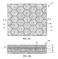
- FIGS. 1A and 1B illustrate an exemplary microwave energy interactive structure 100 according to various aspects of the invention.
- the structure 100 includes a layer of microwave energy interactive material 102, schematically illustrated using stippling in the figures.
- the microwave energy interactive material 102 may be deposited on a microwave energy transparent substrate 104 for ease of handling and/or to prevent contact between the microwave interactive material and a food item (not shown).
- the microwave energy interactive material and substrate collectively form susceptor film 106 ( FIG. 1B ).
- the structure 100 includes a plurality of microwave energy inactive or transparent elements or segments (generally "areas") 108 within the layer of microwave energy interactive material 102.
- the microwave energy interactive material 102 shown by stippling, is generally continuous, except where interrupted by the microwave transparent areas 108, shown in white.
- Each transparent or inactive area may be a portion of the structure from which microwave energy interactive material has been removed chemically or otherwise, may be a portion of the structure formed without a microwave energy interactive material, or may be a portion of the structure formed with a microwave energy interactive material that has been deactivated chemically, mechanically, or otherwise.
- Each transparent or inactive area is circumscribed by the microwave energy interactive material (except those segments that abut an edge of the structure).
- Some of the microwave energy transparent areas 108 are arranged to form a plurality of interconnecting segmented loops 110.
- the segmented loops 110 are substantially hexagonal in shape.
- other shapes for example, circles, squares, rectangles, pentagons, heptagons, or any other regular or irregular shape may be suitable for use with the invention.
- each hexagonal loop 110 is formed from a plurality of microwave energy transparent side elements or segments ("side elements” or “side segments”) 112 and microwave energy transparent corner elements or segments ("corner elements” or “corner segments”) 114. More particularly, each hexagonal loop 110 is formed from 6 pairs of side segments 112 (12 side segments total) and 6 corner segments 114, with the pairs of side segments 112 and corner segments 114 alternating along the loop 110. However, other configurations are contemplated by the invention. For example, the hexagonal loops may be formed from 6 side segments and 6 corner segments, 9 side segments and 6 corner segments, 12 side segments and 6 corner segments, or any other number and arrangement of elements. The combination of side segments 112, corner segments 114, and the microwave energy interactive areas therebetween defines a perimeter P (shown in dashed form) of each loop 110.
- the side segments 112 are substantially rectangular in shape.
- Each side segment 112 has a first dimension D1 and a second dimension D2, for example, a length and a width.
- the corner segments 114 resemble a trio of overlapping substantially rectangular areas or segments, and are referred to herein as having a "tri-star" shape. However, other shapes are contemplated hereby.
- Each of the three “arms" that form the corner segments 114 has a first dimension D3 and a second dimension D4, for example, a length and a width.
- the overall tri-star shape also has a first dimension D5 and a second dimension D6, for example, a length and a width.
- Each of the segments 112 and 114 is separated from an adjacent segment 112 or 114 a distance D7.
- the structure 100 includes a plurality of independent or "floating" microwave energy transparent elements or “islands” 116, each of which is disposed within one of the segmented loops 110 (except those that islands that lie proximate an edge of the structure, which may be within or bordered by only a partial loop).
- the microwave energy transparent elements 116 are substantially cross-shaped.
- the element may be a circle, triangle, square, pentagon, hexagon, star, or any other regular or irregular shape.
- the substantially cross-shaped element 116 may be considered to comprise two orthogonally arranged rectangular segments that overlap at their respective midpoints, or may be viewed as four rectangular "arms" overlapping at one end of each thereof.
- the overlapping rectangular segments or arms may have substantially the same dimensions or may differ from one another.
- each element 116 has a first overall dimension D8 and a second overall dimension D9, for example, a length and a width (either or both of which may correspond to the length of one of the rectangular segments), a third dimension D10, and a fourth dimension D11 corresponding to the respective width of each arm of the cross-shaped element 116.
- the microwave energy transparent element 116 is located substantially centrally within the hexagonal loop 110.
- other arrangements of loops and islands are contemplated hereby.
- Each of the various loops also includes a side length D12, a side to side length (“minor length”) D13, a diametrically opposed, corner to corner length (“major length”) D14, and numerous other specifications that may be used to characterize the various susceptor structures of the invention.
- the arrangement of microwave energy inactive areas may distribute power over the structure, thereby enhancing the heating, browning, and/or crisping of an adjacent food item.
- the array of interconnected segmented loops for example, loops 110 may be dimensioned to induce resonance of microwave energy along each loop and across the array of loops, and therefore may be referred to as "resonant loops".
- the flow of current around each loop increases while the percentage of reflected microwave energy decreases. This, in turn, provides more uniform heating, browning, and/or crisping of the food item.
- the enhanced power distribution across the structure also reduces the potential for overheating, crazing, or charring of the structure in any particular area.
- the peripheral length of the segmented loop (including both microwave energy transparent and microwave energy interactive areas as shown in FIG. 1C ), in this example, hexagonal loop 110, is generally selected to be about one-half of the effective wavelength in an operating microwave oven.
- the effective wavelength in a microwave oven is about 12.0 cm where a susceptor is used (as compared with the theoretical wavelength of 12.24 cm).
- the peripheral length of each hexagonal loop may be selected to be about 6 cm (60 mm).
- other peripheral lengths are contemplated hereby.
- each side segment 112 may have a first dimension, for example, a length D1, of about 2 mm and a second dimension, for example, a width D2, of about 0.5 mm.
- Each "arm" of the tri-star corner segment 114 may have a length D3 of about 1.5 mm and a width D4 of about 0.5 mm.
- the spacing D7 between each side segment 112 and between each rectangular segment 112 and corner segment 114 may be about 1 mm.
- the overall perimeter P of each segmented or broken hexagonal loop 110 may be about 60 mm.
- Each rectangular segment that forms the cross may have a respective length D8 or D9 of about 2 mm and a respective width D10 or D11 of about 0.5 mm.
- the cross-shaped element 116 may have an overall first dimension D8 of about 2 mm and an overall second dimension D9 of about 2 mm.
- the side length D12 may be about 10 mm and the side to side length ("minor length") D13 may be about 17.8 mm.
- Dimension D15 may be about 0.75 mm
- D16 may be about 0.75 mm
- D17 may be about 8.9 mm
- D18 may be about 15.4 mm.
- dimensions D1, D2, D3, D4, D5, D6, D7, D8, D9, D10, and D11 may have any suitable value or may fall within a range of suitable values.
- the side segments 112, corner segments 114, and microwave energy transparent islands or elements each may independently have respective dimensions D1, D2, D3, D4, D5, D6, D7, D8, D9, D10, D11, D15, and/or D16 of from about 0.1 to about 5 mm, from about 0.2 to about 3 mm, from 0.25 to about 0.75 mm, from about 0.3 to about 2.6 mm, from about 0.4 to about 2.5 mm, from about 0.4 to about 0.6, from about 0.5 to 2 mm, from about 0.8 to about 2.2 mm, or from about 1.75 to about 2.25 mm.
- the various dimensions D1, D2, D3, D4, D5, D6, D7, D8, D9, D10, D11, D15, and/or D16 each independently may be about 0.1 mm, about 0.15 mm, about 0.2 mm, about 0.25 mm, about 0.3 mm, about 0.35 mm, about 0.4 mm, about 0.45 mm, about 0.5 mm, about 0.55 mm, about 0.6 mm, about 0.65 mm, about 0.7 mm, about 0.75 mm, about 0.8 mm, about 0.85 mm, about 0.9 mm, about 0.95 mm, about 1 mm, about 1.05 mm, about 1.1 mm, about 1.15 mm, about 1.2 mm, about 1.25 mm, about 1.3 mm, about 1.35 mm, about 1.4 mm, about 1.45 mm, about 1.5 mm, about 1.55 mm, about 1.6 mm, about 1.65 mm, about 1.7 mm, about 1.75 mm, about
- dimensions D12, D13, D14, D17, and D18 may have any suitable value or may fall within a range of suitable values. More particularly, in each of various examples, D12, D13, D14, D17, and/or D18 each independently may be from about 5 to about 25 mm, from about 10 to about 20 mm, from about 12 to about 15 mm, from about 5 to about 10 mm, from about 10 to about 15 mm, from about 15 to about 20 mm, or from about 20 to about 25 mm.
- the various dimensions D12, D13, D17, and/or D18 each independently may be about 5 mm, about 5.5 mm, about 6 mm, about 6.5 mm, about 7 mm, about 7.5 mm, about 8 mm, about 8.5 mm, about 9 mm, about 9.5 mm, about 10 mm, about 10.5 mm, about 11 mm, about 11.5 mm, about 12 mm, about 12.5 mm, about 13 mm, about 13.5 mm, about 14 mm, about 14.5 mm, about 15 mm, about 15.5 mm, about 16 mm, about 16.5 mm, about 17 mm, about 17.5 mm, about 18 mm, about 18.5 mm, about 19 mm, about 19.5 mm, about 20 mm, about 20.5 mm, about 21 mm, about 21.5 mm, about 22 mm, about 22.5 mm, about 23 mm, about 23.5 mm, about 24 mm, about 24.5 mm, or about 25
- the arrangement of microwave energy inactive or transparent areas 108 may control the propagation of any cracks or crazing caused by localized overheating within the structure 100.
- the microwave energy inactive loops 110 and crosses 116 positioned at various respective angles to one another work in concert as a "multidirectional fuse" to manage, control, and terminate the propagation of current, and therefore crazing, between the inactive areas.
- the multidirectional arrangement of inactive areas therefore provides controlled, directional voltage breakage or interruption, rather than random voltage breakage or interruption, thereby resulting in better protection of the structure.
- the crosses can provide only limited, bidirectional protection against crazing of the susceptor.
- the arrangement of microwave energy interactive and microwave energy transparent areas can be selected to provide various levels of heating, as needed or desired for a particular application.
- the substantially rectangular inactive areas could be made to be wider. In doing so, more microwave energy is transmitted to the food item.
- by narrowing the substantially rectangular areas more microwave energy is absorbed, converted into thermal energy, and transmitted to the surface of the food item to enhance browning and/or crisping. Numerous other arrangements and configurations are contemplated hereby.
- the microwave energy interactive material may be an electroconductive or semiconductive material, for example, a metal or a metal alloy provided as a metal foil; a vacuum deposited metal or metal alloy; or a metallic ink, an organic ink, an inorganic ink, a metallic paste, an organic paste, an inorganic paste, or any combination thereof.
- metals and metal alloys that may be suitable for use with the present invention include, but are not limited to, aluminum, chromium, copper, inconel alloys (nickel-chromium-molybdenum alloy with niobium), iron, magnesium, nickel, stainless steel, tin, titanium, tungsten, and any combination or alloy thereof.
- the microwave energy interactive material may comprise a metal oxide.
- metal oxides that may be suitable for use with the present invention include, but are not limited to, oxides of aluminum, iron, and tin, used in conjunction with an electrically conductive material where needed.
- ITO indium tin oxide
- ITO can be used as a microwave energy interactive material to provide a heating effect, a shielding effect, a browning and/or crisping effect, or a combination thereof.
- ITO may be sputtered onto a clear polymer film. The sputtering process typically occurs at a lower temperature than the evaporative deposition process used for metal deposition.
- ITO has a more uniform crystal structure and, therefore, is clear at most coating thicknesses. Additionally, ITO can be used for either heating or field management effects. ITO also may have fewer defects than metals, thereby making thick coatings of ITO more suitable for field management than thick coatings of metals, such as aluminum.
- the microwave energy interactive material may comprise a suitable electroconductive, semiconductive, or non-conductive artificial dielectric or ferroelectric.
- Artificial dielectrics comprise conductive, subdivided material in a polymer or other suitable matrix or binder, and may include flakes of an electroconductive metal, for example, aluminum.
- the substrate typically comprises an electrical insulator, for example, a polymer film or other polymeric material.
- an electrical insulator for example, a polymer film or other polymeric material.
- polymer polymer film or other polymeric material
- polymeric material include, but are not limited to, homopolymers, copolymers, such as for example, block, graft, random, and alternating copolymers, terpolymers, etc. and blends and modifications thereof.
- the term “polymer” shall include all possible geometrical configurations of the molecule. These configurations include, but are not limited to isotactic, syndiotactic, and random symmetries.
- the thickness of the film typically may be from about 35 gauge to about 10 mil. In one aspect, the thickness of the film is from about 40 to about 80 gauge. In another aspect, the thickness of the film is from about 45 to about 50 gauge. In still another aspect, the thickness of the film is about 48 gauge.
- Examples of polymer films that may be suitable include, but are not limited to, polyolefins, polyesters, polyamides, polyimides, polysulfones, polyether ketones, cellophanes, or any combination thereof.
- Other non-conducting substrate materials such as paper and paper laminates, metal oxides, silicates, cellulosics, or any combination thereof, also may be used.
- the polymer film comprises polyethylene terephthalate (PET).
- PET polyethylene terephthalate
- Polyethylene terephthalate films are used in commercially available susceptors, for example, the QWIKWAVE ® Focus susceptor and the MICRORITE ® susceptor, both available from Graphic Packaging International (Marietta, Georgia).
- Examples of polyethylene terephthalate films that may be suitable for use as the substrate include, but are not limited to, MELINEX ® , commercially available from DuPont Teijan Films (Hopewell, Virginia), SKYROL, commercially available from SKC, Inc.
- the polymer film comprises polyethylene terephthalate having a thickness of about 48 gauge. In another particular example, the polymer film comprises heat sealable polyethylene terephthalate having a thickness of about 48 gauge.
- the polymer film may be selected to impart various properties to the microwave interactive web, for example, printability, heat resistance, or any other property.
- the polymer film may be selected to provide a water barrier, oxygen barrier, or a combination thereof.
- barrier film layers may be formed from a polymer film having barrier properties or from any other barrier layer or coating as desired.
- Suitable polymer films may include, but are not limited to, ethylene vinyl alcohol, barrier nylon, polyvinylidene chloride, barrier fluoropolymer, nylon 6, nylon 6,6, coextruded nylon 6/EVOH/nylon 6, silicon oxide coated film, barrier polyethylene terephthalate, or any combination thereof.
- Another example of a barrier film that may be suitable is CAPRAN® OXYSHIELD OBS monoaxially oriented coextruded nylon 6/ethylene vinyl alcohol (EVOH)/nylon 6, also commercially available from Honeywell International.
- Yet another example of a barrier film that may be suitable for use with the present invention is DARTEK® N-201 nylon 6,6, commercially available from Enhance Packaging Technologies (Webster, New York). Additional examples include BARRIALOX PET, available from Toray Films (Front Royal, VA) and QU50 High Barrier Coated PET, available from Toray Films (Front Royal, VA), referred to above.
- a susceptor may have a structure including a film, for example, polyethylene terephthalate, with a layer of silicon oxide coated onto the film, and ITO or other material deposited over the silicon oxide. If needed or desired, additional layers or coatings may be provided to shield the individual layers from damage during processing.
- the barrier film may have an oxygen transmission rate (OTR) as measured using ASTM D3985 of less than about 20 cc/m 2 /day.
- OTR oxygen transmission rate
- the barrier film has an OTR of less than about 10 cc/m 2 /day.
- the barrier film has an OTR of less than about 1 cc/m 2 /day.
- the barrier film has an OTR of less than about 0.5 cc/m 2 /day.
- the barrier film has an OTR of less than about 0.1 cc/m 2 /day.
- the barrier film may have a water vapor transmission rate (WVTR) of less than about 100 g/m 2 /day as measured using ASTM F1249. In one aspect, the barrier film has a water vapor transmission rate as measured using ASTM F1249 of less than about 50 g/m 2 /day. In another aspect, the barrier film has a WVTR of less than about 15 g/m 2 /day. In yet another aspect, the barrier film has a WVTR of less than about 1 g/m 2 /day. In still another aspect, the barrier film has a WVTR of less than about 0.1 g/m 2 /day. In a still further aspect, the barrier film has a WVTR of less than about 0.05 g/m 2 /day.
- WVTR water vapor transmission rate
- non-conducting substrate materials such as metal oxides, silicates, cellulosics, or any combination thereof, also may be used in accordance with the invention.
- the microwave energy interactive material may be applied to the substrate in any suitable manner, and in some instances, the microwave energy interactive material is printed on, extruded onto, sputtered onto, evaporated on, or laminated to the substrate.
- the microwave energy interactive material may be applied to the substrate in any pattern, and using any technique, to achieve the desired heating effect of the food item.
- the microwave energy interactive material may be provided as a continuous or discontinuous layer or coating including circles, loops, hexagons, islands, squares, rectangles, octagons, and so forth. Examples of various patterns and methods that may be suitable for use with the present invention are provided in U.S. Patent Nos.
- the susceptor film 106 may be joined at least partially to a dimensionally stable support 118 using a continuous or discontinuous layer adhesive or other suitable material 120 (shown as continuous in FIG. 1B ).
- all or a portion of the support may be formed at least partially from a paperboard material having a basis weight of from about 60 to about 330 lbs/ream, for example, from about 80 to about 140 lbs/ream.
- the paperboard generally may have a thickness of from about 6 to about 30 mils, for example, from about 12 to about 28 mils. In one particular example, the paperboard has a thickness of about 12 mils.
- Any suitable paperboard may be used, for example, a solid bleached or solid unbleached sulfate board, such as SUS® board, commercially available from Graphic Packaging International.
- the support 118 may comprise a paper or paper-based material generally having a basis weight of from about 15 to about 60 lbs/ream, for example, from about 20 to about 40 lbs/ream. In one particular example, the paper has a basis weight of about 25 lbs/ream.
- the susceptor 106 may be joined to the support 118 in any manner and using any suitable material, for example, a binding layer or adhesive 120.
- the layers are joined using a layer of a polyolefin, for example, polypropylene, polyethylene, low density polyethylene, or any other polymer or combination of polymers.
- a polyolefin for example, polypropylene, polyethylene, low density polyethylene, or any other polymer or combination of polymers.
- other adhesives are contemplated hereby.
- the adhesive may have a basis weight or dry coat weight of from about 3 to about 18 lb/ream. In one example, the adhesive may have a dry coat weight of from about 5 to about 15 lb/ream. In another example, the adhesive may have a dry coat weight of from about 8 to about 12 lb/ream.
- the microwave interactive element for example, element 102
- the microwave interactive element may have a grey or silver color that is visually distinguishable from the substrate or the support.
- the present invention contemplates using a silver or grey toned adhesive to join the microwave interactive elements to the substrate, using a silver or grey toned substrate to mask the presence of the silver or grey toned microwave interactive element, using a dark toned substrate, for example, a black toned substrate, to conceal the presence of the silver or grey toned microwave interactive element, overprinting the metallized side of the web with a silver or grey toned ink to obscure the color variation, printing the non-metallized side of the web with a silver or grey ink or other concealing color in a suitable pattern or as a solid color layer to mask or conceal the presence of the microwave interactive element, or any other suitable technique or combination thereof.
- High Power RAT Each sample evaluated for high power RAT was subjected to an increasing E-field strength using a Magnetron microwave power generator. The input power, reflected power, and transmitted power were measured and the RAT values were reported.
- Each susceptor structure evaluated was cut into a sample having a size of about 2 in. x 4 in. and mounted in a cardboard frame. One at a time, the samples were placed on the auto macro-stage of a Leica QWIN Image Analysis System. The samples were illuminated by four flood lamps that provided incident omni-directional darkfield illumination.
- the cracks on the susceptor structures were examined with a macro lens, and Leica DFC 350 camera, sufficient to image a 1 cm wide field-of-view (FOV). Twenty-eight (28) 1 cm fields were scanned using auto-stage motion in a non-adjacent 4 x 7 matrix, with a stop at each field position for focus, lighting, and threshold adjustments needed to compensate for sample buckling, illumination variability, and background scorching.
- the cracks were detected in auto-delineation mode using various steps of binary "open” and “close” operations, combined with image subtraction, to remove noise and the intentionally imparted microwave energy transparent areas (e.g., segmented hexagonal loops and crosses).
- image processing and procedures listed above are known to those proficient in the art of image analysis.
- An exemplary susceptor film according to the invention having an optical density of about 0.26 was laminated to paper having a basis weight of about 35 lb/ream.
- the susceptor film was substantially similar to the structure shown schematically in FIG. 1D , except for variations that will be understood by those in the art.
- D1 was about 2 mm
- D2 was about 0.5 mm
- D2 was about 1.5 mm
- D4 was about 0.5 mm
- D7 was about 1 mm
- D8 was about 2 mm
- D9 was about 2 mm
- D10 was about 0.5 mm
- D11 was about 0.5 mm
- D12 was about 10 mm
- D13 was about 17.8,
- D15 was about 0.75 mm
- D16 was about 0.75 mm
- D17 was about 8.9 mm
- D18 was about 15.4 mm.
- Six samples were prepared and evaluated for low power RAT. Each sample was tested in the machine direction and the cross machine direction. The results are presented in Table 2.
- Table 2. Samples 1-6 R (%) A (%) T (%) MF (%) Average (%) 47.3 42.4 10.3 80.6 Standard deviation (%) 3.6 2.4 2.1 3.1 Maximum (%) 51 84 48 84 Minimum (%) 40 39 8 76
- Samples 1-6 also were subjected to open load testing in a microwave oven. Each sample sustained heating for a period of greater than 120 seconds without creating a fire.
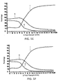
- Table 3 The structure also was evaluated for high power RAT. The results are presented in Table 3 and FIG. 1E (Sample 7, oriented in the machine direction), Table 4 and FIG. 1F (Sample 8, oriented in the cross machine direction), Table 5 and FIG. 1G (Sample 9, oriented in the machine direction), and Table 6 and FIG. 1H (Sample 10, oriented in the cross machine direction). Table 3.
- a plain susceptor film having an optical density of about 0.26 was laminated to paper having a basis weight of about 35 lb/ream. Twelve samples were prepared and evaluated to determine the low power RAT characteristics. Each sample was tested in the machine direction and the cross machine direction. The results are presented in Table 7. Table 7. Samples 11-22 R (%) A (%) T (%) MF (%) Average (%) 49 42.3 8.4 83.5 Standard deviation (%) 1.5 1.0 0.6 0.7 Maximum (%) 53 44 9 85 Minimum (%) 46 40 7 83
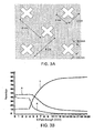
- a susceptor film with a simple cross pattern substantially as shown schematically in FIG. 3A (available commercially from Graphic Packaging International, Inc. (Marietta, Georgia)), was laminated to paper having a basis weight of about 35 lb/ream. Twenty-four samples were prepared and evaluated to determine the low power RAT characteristics of the structure. Each sample was tested in the machine direction and the cross-machine direction. The results are presented in Table 10. Table 10. Samples 25-48 R (%) A (%) T (%) MF (%) Average (%) 44.9 45.1 9.7 82.4 Standard deviation (%) 3.1 2.6 2.1 3.2 Maximum (%) 39 41 7 75 Minimum (%) 51 51 15 87
- Table 11 The structure also was subjected to high power RAT testing. The results are presented in Table 11 and FIG. 3B (Sample 49, oriented in the machine direction), Table 12 and FIG. 3C (Sample 50, oriented in the machine direction), and Table 13 and FIG. 3D (Sample 51, oriented in the cross machine direction). Table 11.
- Samples 52-57 also were subjected to open load testing in a microwave ovens. Each of the samples sustained heating for a period of greater than 120 seconds without creating a fire.
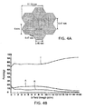
- the structure also was evaluated to determine high power RAT characteristics.
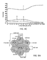
- the results are presented in Table 15 and FIG. 4B (Sample 58, oriented in the machine direction), and Table 16 and FIG. 4C (Sample 59, oriented in the cross machine direction). Table 15.
- Samples 60-65 also were subjected to open load testing in a microwave ovens. Each of the samples sustained heating for a period of greater than 120 seconds without creating a fire.
- the structure also was evaluated to determine high power RAT characteristics.
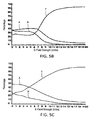
- the results are presented in Table 18 and FIG. 5B (Sample 66, oriented in the machine direction), and Table 19 and FIG. 5C (Sample 67, oriented in the cross machine direction). Table 18.
- Table 20 Structure Description Plain paper Plain susceptor film having an optical density of about 0.26, laminated to paper having a basis weight of about 35 lb/ream (lb/3000 sq. ft.) Plain board Plain susceptor film having an optical density of about 0.26, laminated to paperboard having a caliper of about 23.5 pt (about 247 lb/ream) Cross paper Susceptor film with a simple cross pattern, as shown in FIG. 3A , laminated to paper having a basis weight of about 35 lb/ream Cross board Susceptor film with a simple cross pattern, as shown in FIG.
- FIG. 3A laminated to paperboard having a caliper of about 14.5 pt (about 152 lb/ream) Hex fuse paper
- FIG. 1D laminated to paper having a basis weight of about 35 lb/ream Hex fuse board
- FIG. 1D laminated to paperboard having a caliper of about 23.5 pt (about 247 lb/ream)
Landscapes
- Engineering & Computer Science (AREA)
- Life Sciences & Earth Sciences (AREA)
- Food Science & Technology (AREA)
- Mechanical Engineering (AREA)
- Constitution Of High-Frequency Heating (AREA)
- Cookers (AREA)
- Fuses (AREA)
- Details Of Aerials (AREA)
- Fixing For Electrophotography (AREA)
- Surface Treatment Of Glass (AREA)
- Design And Manufacture Of Integrated Circuits (AREA)
- Switches With Compound Operations (AREA)
- Electric Ovens (AREA)
Abstract
Description
- This application claims the benefit of
U.S. Provisional Application No. 60/795,320, filed April 27, 2006 U.S. Provisional Application No. 60/890,037, filed February 15, 2007 - The present invention relates generally to microwave energy interactive structures and, more particularly, the present invention relates generally to microwave energy interactive structures that are capable of heating, browning, and/or crisping an adjacent food item.
- The use of susceptors in food packaging for microwavable food items is well known to those in the art. The susceptor converts microwave energy to thermal energy, which then can be transferred to an adjacent food item. As a result, the heating, browning, and/or crisping of the food item can be enhanced. With a conventional plain susceptor film, there is a random flow of current under microwave energy radiation. The magnitude of the current flow depends on the surface resistance of the susceptor, which is related to the random distribution of fine metallic spots and the E-field strength applied to the sheet. If the magnitude of the current is high enough, or a susceptor is used in a package without a uniform food load, the susceptor film may overheat at one or more regions and cause crazing or shrinking of the susceptor film. As a result, the ability of the susceptor to generate heat is diminished. Thus, there is a need for a microwave energy interactive structure that enhances heating, browning, and/or crisping of an adjacent food item while being resistant to burning, crazing, and scorching.
- According to the present invention, a susceptor structure is provided with a plurality of microwave energy transparent areas that reduce or prevent large scale random current flow. The microwave energy inactive areas are arranged as a pattern of segments that define a plurality of generally interconnected shapes. In one exemplary embodiment, a microwave energy transparent element is substantially centrally located within each shape.
- In one aspect, the interconnected shapes are dimensioned to create a resonant effect in the presence of microwave energy. The resonant effect of the interconnected shapes provides uniform power distribution and, therefore, uniform heating, across the structure.
- In another aspect, the interconnected shapes form a "multidirectional fuse". The multidirectional fuse includes a plurality of selectively arranged microwave energy transparent areas that limit the random flow of current and random crazing typically observed with conventional susceptor structures.
- As a result of these and other aspects, the susceptor structure of the invention is less susceptible to crazing, and therefore, is less susceptible to premature failure. As such, the susceptor structure of the invention can withstand higher power levels and has a greater useful life, while still having an innate ability to self-limit or "shut down" to avoid undesirable overheating.
- In one particular aspect, the invention is directed to a susceptor structure comprising a layer of conductive material supported on a non-conductive substrate, where the conductive layer includes a resonant loop defined by a plurality of microwave energy transparent segments and a microwave energy transparent element within the resonant loop. The resonant loop may be substantially hexagonal in shape or may have any other suitable shape, and may be formed from side segments and corner segments.
- In one variation, the side segments of the resonant loop have a substantially rectangular shape. In another variation, the side segments of the resonant loop may have a first dimension of about 2 mm and, optionally, a second dimension of about 0.5 mm. In another variation, the corner segments have a substantially tri-star shape.
- In still another variation, the microwave energy transparent element within the resonant loop is substantially cross-shaped. The microwave energy transparent element within the resonant loop may comprise a pair of orthogonally overlapping, substantially rectangular microwave energy transparent segments. Each of the substantially rectangular microwave energy transparent segments may have an overall first dimension of about 2 mm and an overall second dimension of about 2 mm. If desired, the microwave energy transparent element within the resonant loop may be substantially centered within the resonant loop. The resonant loop may have a perimeter of about 60 mm.
- In another aspect, the invention is directed to a susceptor structure comprising a plurality of microwave energy transparent segments within a layer of microwave energy interactive material and a substantially cross-shaped microwave energy transparent element substantially centered within the hexagonal loop. The microwave energy transparent segments are arranged in the shape of a hexagonal loop.
- In one variation, the plurality of microwave energy transparent segments may include segments that form sides of the hexagonal loop and segments that form corners of the hexagonal loop. In another variation, the segments that form sides of the hexagonal loop have a first dimension of about 2 mm and a second dimension of about 0.5 mm, the corner segments are substantially tri-star in shape, the cross-shaped element substantially centered within the hexagonal loop has a first overall dimension of about 2 mm and a second overall dimension of about 2 mm, and the perimeter of the hexagonal loop is about 60 mm.
- In yet another aspect, the invention is directed to a susceptor structure comprising a layer of conductive material supported on a non-conductive substrate. The conductive layer includes a plurality of spaced apart microwave energy transparent segments that define a pattern of interconnected hexagonal loops, and a substantially centrally located microwave energy transparent element within at least one of the loops.
- The plurality of spaced apart microwave energy transparent segments may include side segments and corner segments. In one variation, the side segments have a substantially rectangular shape. In another variation, the corner segments have a substantially tri-star shape. The substantially centrally located microwave energy transparent element within at least one of the loops may have a substantially cross shape.
- Each of the hexagonal loops may have a perimeter selected to promote resonance of microwave energy along each hexagonal loop. Further, each of the hexagonal loops may have a perimeter selected to promote resonance of microwave energy across the susceptor structure. For example, the perimeter of each of the hexagonal loops may have a perimeter approximately equal to one-half of an effective wavelength of an operating microwave oven.
- In a further aspect, the invention is directed to a susceptor structure comprising an electrically continuous layer of conductive material supported on a non-conductive substrate. The susceptor structure includes a repeating pattern of microwave energy transparent areas within the layer of conductive material. The microwave energy transparent areas generally are circumscribed by the layer of conductive material. The repeating pattern includes a plurality of cross-shaped microwave energy transparent elements and a plurality of a microwave energy transparent, segmented hexagonal loops. Each cross-shaped microwave energy transparent element is disposed within one of the segmented hexagonal loops. The hexagonal loops are dimensioned to promote resonance of microwave energy across the susceptor structure. In one variation, the electrically continuous layer of conductive material comprises aluminum, the non-conductive substrate comprises a polymer film, the cross-shaped microwave energy transparent elements each have a first dimension of about 2 mm and a second dimension of about 2 mm, and the hexagonal loops each have a perimeter of about 60 mm.
- Other features, aspects, and embodiments will be apparent from the following description and accompanying figures.
- The description refers to the accompanying drawings, some of which are schematic, in which like reference characters refer to like parts throughout the several views, and in which:
-
FIG. 1A schematically depicts an exemplary microwave energy interactive structure according to various aspects of the invention; -
FIG. 1B schematically depicts a cross-sectional view of the structure ofFIG. 1A taken along aline 1B-1B; -
FIG. 1C schematically depicts a segmented loop according to various aspects of the invention; -
FIG. 1D schematically depicts an enlarged view of the arrangement of microwave energy interactive and transparent elements ofFIG. 1A , according to various aspects of the invention; -
FIGS. 1E-1H present the reflection-absorption-transmission characteristics of the arrangement ofFIG. 1D under open load, high power conditions; -
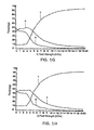
FIGS. 2A and 2B present the reflection-absorption-transmission characteristics of a plain susceptor film joined to paper under open load, high power conditions, for comparative purposes; -
FIG. 3A schematically depicts another exemplary arrangement of microwave energy interactive and transparent elements, with approximate dimensions; -
FIGS. 3B-3D present the reflection-absorption-transmission characteristics of the arrangement ofFIG. 3A under open load, high power conditions; -
FIG. 4A schematically depicts still another exemplary arrangement of microwave energy interactive and transparent elements, with approximate dimensions; -
FIGS. 4B and4C present the reflection-absorption-transmission characteristics of the arrangement ofFIG. 4A under open load, high power conditions; -
FIG. 5A schematically depicts yet another exemplary arrangement of microwave energy interactive and transparent elements, with approximate dimensions; and -
FIGS. 5B and 5C present the reflection-absorption-transmission characteristics of the arrangement ofFIG. 5A under open load, high power conditions. - The present invention may be illustrated further by referring to the figures. For purposes of simplicity, like numerals may be used to describe like features. It will be understood that where a plurality of similar features are depicted, not all of such features necessarily are labeled on each figure. It also will be understood that various components used to form the microwave energy interactive structures of the invention may be interchanged. Thus, while only certain combinations are illustrated herein, numerous other combinations and configurations are contemplated hereby.
-
FIGS. 1A and 1B illustrate an exemplary microwave energyinteractive structure 100 according to various aspects of the invention. Thestructure 100 includes a layer of microwave energyinteractive material 102, schematically illustrated using stippling in the figures. The microwave energyinteractive material 102 may be deposited on a microwave energytransparent substrate 104 for ease of handling and/or to prevent contact between the microwave interactive material and a food item (not shown). The microwave energy interactive material and substrate collectively form susceptor film 106 (FIG. 1B ). - As shown in
FIGS. 1A and 1B , thestructure 100 includes a plurality of microwave energy inactive or transparent elements or segments (generally "areas") 108 within the layer of microwave energyinteractive material 102. The microwave energyinteractive material 102, shown by stippling, is generally continuous, except where interrupted by the microwavetransparent areas 108, shown in white. Each transparent or inactive area may be a portion of the structure from which microwave energy interactive material has been removed chemically or otherwise, may be a portion of the structure formed without a microwave energy interactive material, or may be a portion of the structure formed with a microwave energy interactive material that has been deactivated chemically, mechanically, or otherwise. Each transparent or inactive area is circumscribed by the microwave energy interactive material (except those segments that abut an edge of the structure). - Some of the microwave energy
transparent areas 108 are arranged to form a plurality of interconnectingsegmented loops 110. In this example, thesegmented loops 110 are substantially hexagonal in shape. However, other shapes, for example, circles, squares, rectangles, pentagons, heptagons, or any other regular or irregular shape may be suitable for use with the invention. - As best seen in
FIG. 1C , eachhexagonal loop 110 is formed from a plurality of microwave energy transparent side elements or segments ("side elements" or "side segments") 112 and microwave energy transparent corner elements or segments ("corner elements" or "corner segments") 114. More particularly, eachhexagonal loop 110 is formed from 6 pairs of side segments 112 (12 side segments total) and 6corner segments 114, with the pairs ofside segments 112 andcorner segments 114 alternating along theloop 110. However, other configurations are contemplated by the invention. For example, the hexagonal loops may be formed from 6 side segments and 6 corner segments, 9 side segments and 6 corner segments, 12 side segments and 6 corner segments, or any other number and arrangement of elements. The combination ofside segments 112,corner segments 114, and the microwave energy interactive areas therebetween defines a perimeter P (shown in dashed form) of eachloop 110. - In this example, the
side segments 112 are substantially rectangular in shape. Eachside segment 112 has a first dimension D1 and a second dimension D2, for example, a length and a width. Thecorner segments 114 resemble a trio of overlapping substantially rectangular areas or segments, and are referred to herein as having a "tri-star" shape. However, other shapes are contemplated hereby. Each of the three "arms" that form thecorner segments 114 has a first dimension D3 and a second dimension D4, for example, a length and a width. The overall tri-star shape also has a first dimension D5 and a second dimension D6, for example, a length and a width. Each of thesegments adjacent segment 112 or 114 a distance D7. - Additionally, the
structure 100 includes a plurality of independent or "floating" microwave energy transparent elements or "islands" 116, each of which is disposed within one of the segmented loops 110 (except those that islands that lie proximate an edge of the structure, which may be within or bordered by only a partial loop). In this example, the microwave energytransparent elements 116 are substantially cross-shaped. However, it will be understood that the element may be a circle, triangle, square, pentagon, hexagon, star, or any other regular or irregular shape. - The substantially
cross-shaped element 116 may be considered to comprise two orthogonally arranged rectangular segments that overlap at their respective midpoints, or may be viewed as four rectangular "arms" overlapping at one end of each thereof. The overlapping rectangular segments or arms may have substantially the same dimensions or may differ from one another. In any case, eachelement 116 has a first overall dimension D8 and a second overall dimension D9, for example, a length and a width (either or both of which may correspond to the length of one of the rectangular segments), a third dimension D10, and a fourth dimension D11 corresponding to the respective width of each arm of thecross-shaped element 116. In this example, the microwave energytransparent element 116 is located substantially centrally within thehexagonal loop 110. However, other arrangements of loops and islands are contemplated hereby. - Each of the various loops also includes a side length D12, a side to side length ("minor length") D13, a diametrically opposed, corner to corner length ("major length") D14, and numerous other specifications that may be used to characterize the various susceptor structures of the invention.
- In one aspect, the arrangement of microwave energy inactive areas may distribute power over the structure, thereby enhancing the heating, browning, and/or crisping of an adjacent food item. More particularly, the array of interconnected segmented loops, for example,
loops 110 may be dimensioned to induce resonance of microwave energy along each loop and across the array of loops, and therefore may be referred to as "resonant loops". As a result, the flow of current around each loop increases while the percentage of reflected microwave energy decreases. This, in turn, provides more uniform heating, browning, and/or crisping of the food item. Further, the enhanced power distribution across the structure also reduces the potential for overheating, crazing, or charring of the structure in any particular area. - To create the resonant effect, the peripheral length of the segmented loop (including both microwave energy transparent and microwave energy interactive areas as shown in
FIG. 1C ), in this example,hexagonal loop 110, is generally selected to be about one-half of the effective wavelength in an operating microwave oven. For example, it has been observed that the effective wavelength in a microwave oven is about 12.0 cm where a susceptor is used (as compared with the theoretical wavelength of 12.24 cm). In such an example, the peripheral length of each hexagonal loop may be selected to be about 6 cm (60 mm). However, other peripheral lengths are contemplated hereby. - Numerous exemplary values for the various dimensions or specifications for an exemplary arrangement of elements is provided with reference to
FIG. 1D , in which a pattern of resonant hexagonal "fuse"loops 110 is provided in a susceptor structure, for example, susceptor structure 100 (FIG. 1A ), with the microwave energyinteractive material 102 being shown schematically by stippling. For example, eachside segment 112 may have a first dimension, for example, a length D1, of about 2 mm and a second dimension, for example, a width D2, of about 0.5 mm. Each "arm" of thetri-star corner segment 114 may have a length D3 of about 1.5 mm and a width D4 of about 0.5 mm. The spacing D7 between eachside segment 112 and between eachrectangular segment 112 andcorner segment 114 may be about 1 mm. The overall perimeter P of each segmented or brokenhexagonal loop 110 may be about 60 mm. Each rectangular segment that forms the cross may have a respective length D8 or D9 of about 2 mm and a respective width D10 or D11 of about 0.5 mm. Thecross-shaped element 116 may have an overall first dimension D8 of about 2 mm and an overall second dimension D9 of about 2 mm. The side length D12 may be about 10 mm and the side to side length ("minor length") D13 may be about 17.8 mm. Dimension D15 may be about 0.75 mm, D16 may be about 0.75 mm, D17 may be about 8.9 mm, and D18 may be about 15.4 mm. - It will be understood that the various dimensions that define a particular susceptor structure may vary for each application. As such, numerous other dimensions and ranges of dimensions are contemplated hereby.
- Thus, in each of various examples, dimensions D1, D2, D3, D4, D5, D6, D7, D8, D9, D10, and D11 may have any suitable value or may fall within a range of suitable values. More particularly, the
side segments 112,corner segments 114, and microwave energy transparent islands or elements each may independently have respective dimensions D1, D2, D3, D4, D5, D6, D7, D8, D9, D10, D11, D15, and/or D16 of from about 0.1 to about 5 mm, from about 0.2 to about 3 mm, from 0.25 to about 0.75 mm, from about 0.3 to about 2.6 mm, from about 0.4 to about 2.5 mm, from about 0.4 to about 0.6, from about 0.5 to 2 mm, from about 0.8 to about 2.2 mm, or from about 1.75 to about 2.25 mm. - Still more particularly, in each of various examples, the various dimensions D1, D2, D3, D4, D5, D6, D7, D8, D9, D10, D11, D15, and/or D16 each independently may be about 0.1 mm, about 0.15 mm, about 0.2 mm, about 0.25 mm, about 0.3 mm, about 0.35 mm, about 0.4 mm, about 0.45 mm, about 0.5 mm, about 0.55 mm, about 0.6 mm, about 0.65 mm, about 0.7 mm, about 0.75 mm, about 0.8 mm, about 0.85 mm, about 0.9 mm, about 0.95 mm, about 1 mm, about 1.05 mm, about 1.1 mm, about 1.15 mm, about 1.2 mm, about 1.25 mm, about 1.3 mm, about 1.35 mm, about 1.4 mm, about 1.45 mm, about 1.5 mm, about 1.55 mm, about 1.6 mm, about 1.65 mm, about 1.7 mm, about 1.75 mm, about 1.8 mm, about 1.85 mm, about 1.9 mm, about 1.95 mm, about 2 mm, about 2.05 mm, about 2.1 mm, about 2.15 mm, about 2.2 mm, about 2.25 mm, about 2.3 mm, about 2.35 mm, about 2.4 mm, about 2.45 mm, about 2.5 mm, about 2.55 mm, about 2.6 mm, about 2.65 mm, about 2.7 mm, about 2.75 mm, about 2.8 mm, about 2.85 mm, about 2.9 mm, about 2.95 mm, or about 3 mm. Other values and ranges of values are contemplated hereby.
- Likewise, in each of various examples, dimensions D12, D13, D14, D17, and D18 may have any suitable value or may fall within a range of suitable values. More particularly, in each of various examples, D12, D13, D14, D17, and/or D18 each independently may be from about 5 to about 25 mm, from about 10 to about 20 mm, from about 12 to about 15 mm, from about 5 to about 10 mm, from about 10 to about 15 mm, from about 15 to about 20 mm, or from about 20 to about 25 mm.
- Still more particularly, in each of various examples, the various dimensions D12, D13, D17, and/or D18 each independently may be about 5 mm, about 5.5 mm, about 6 mm, about 6.5 mm, about 7 mm, about 7.5 mm, about 8 mm, about 8.5 mm, about 9 mm, about 9.5 mm, about 10 mm, about 10.5 mm, about 11 mm, about 11.5 mm, about 12 mm, about 12.5 mm, about 13 mm, about 13.5 mm, about 14 mm, about 14.5 mm, about 15 mm, about 15.5 mm, about 16 mm, about 16.5 mm, about 17 mm, about 17.5 mm, about 18 mm, about 18.5 mm, about 19 mm, about 19.5 mm, about 20 mm, about 20.5 mm, about 21 mm, about 21.5 mm, about 22 mm, about 22.5 mm, about 23 mm, about 23.5 mm, about 24 mm, about 24.5 mm, or about 25 mm.
- In another aspect, the arrangement of microwave energy inactive or
transparent areas 108 may control the propagation of any cracks or crazing caused by localized overheating within thestructure 100. The microwave energyinactive loops 110 and crosses 116 positioned at various respective angles to one another work in concert as a "multidirectional fuse" to manage, control, and terminate the propagation of current, and therefore crazing, between the inactive areas. The multidirectional arrangement of inactive areas therefore provides controlled, directional voltage breakage or interruption, rather than random voltage breakage or interruption, thereby resulting in better protection of the structure. In a structure without the hexagonal loops, such as that shown inU.S. Patent Nos. 5,412,187 and5,530,231 , the crosses can provide only limited, bidirectional protection against crazing of the susceptor. - The arrangement of microwave energy interactive and microwave energy transparent areas can be selected to provide various levels of heating, as needed or desired for a particular application. For example, where greater heating is desired, the substantially rectangular inactive areas could be made to be wider. In doing so, more microwave energy is transmitted to the food item. Alternatively, by narrowing the substantially rectangular areas, more microwave energy is absorbed, converted into thermal energy, and transmitted to the surface of the food item to enhance browning and/or crisping. Numerous other arrangements and configurations are contemplated hereby.
- The microwave energy interactive material may be an electroconductive or semiconductive material, for example, a metal or a metal alloy provided as a metal foil; a vacuum deposited metal or metal alloy; or a metallic ink, an organic ink, an inorganic ink, a metallic paste, an organic paste, an inorganic paste, or any combination thereof. Examples of metals and metal alloys that may be suitable for use with the present invention include, but are not limited to, aluminum, chromium, copper, inconel alloys (nickel-chromium-molybdenum alloy with niobium), iron, magnesium, nickel, stainless steel, tin, titanium, tungsten, and any combination or alloy thereof.
- Alternatively, the microwave energy interactive material may comprise a metal oxide. Examples of metal oxides that may be suitable for use with the present invention include, but are not limited to, oxides of aluminum, iron, and tin, used in conjunction with an electrically conductive material where needed. Another example of a metal oxide that may be suitable for use with the present invention is indium tin oxide (ITO). ITO can be used as a microwave energy interactive material to provide a heating effect, a shielding effect, a browning and/or crisping effect, or a combination thereof. For example, to form a susceptor, ITO may be sputtered onto a clear polymer film. The sputtering process typically occurs at a lower temperature than the evaporative deposition process used for metal deposition. ITO has a more uniform crystal structure and, therefore, is clear at most coating thicknesses. Additionally, ITO can be used for either heating or field management effects. ITO also may have fewer defects than metals, thereby making thick coatings of ITO more suitable for field management than thick coatings of metals, such as aluminum.
- Alternatively, the microwave energy interactive material may comprise a suitable electroconductive, semiconductive, or non-conductive artificial dielectric or ferroelectric. Artificial dielectrics comprise conductive, subdivided material in a polymer or other suitable matrix or binder, and may include flakes of an electroconductive metal, for example, aluminum.
- The substrate typically comprises an electrical insulator, for example, a polymer film or other polymeric material. As used herein the terms "polymer", "polymer film", and "polymeric material" include, but are not limited to, homopolymers, copolymers, such as for example, block, graft, random, and alternating copolymers, terpolymers, etc. and blends and modifications thereof. Furthermore, unless otherwise specifically limited, the term "polymer" shall include all possible geometrical configurations of the molecule. These configurations include, but are not limited to isotactic, syndiotactic, and random symmetries.
- The thickness of the film typically may be from about 35 gauge to about 10 mil. In one aspect, the thickness of the film is from about 40 to about 80 gauge. In another aspect, the thickness of the film is from about 45 to about 50 gauge. In still another aspect, the thickness of the film is about 48 gauge. Examples of polymer films that may be suitable include, but are not limited to, polyolefins, polyesters, polyamides, polyimides, polysulfones, polyether ketones, cellophanes, or any combination thereof. Other non-conducting substrate materials such as paper and paper laminates, metal oxides, silicates, cellulosics, or any combination thereof, also may be used.
- In one example, the polymer film comprises polyethylene terephthalate (PET). Polyethylene terephthalate films are used in commercially available susceptors, for example, the QWIKWAVE® Focus susceptor and the MICRORITE® susceptor, both available from Graphic Packaging International (Marietta, Georgia). Examples of polyethylene terephthalate films that may be suitable for use as the substrate include, but are not limited to, MELINEX®, commercially available from DuPont Teijan Films (Hopewell, Virginia), SKYROL, commercially available from SKC, Inc. (Covington, Georgia), and BARRIALOX PET, available from Toray Films (Front Royal, VA), and QU50 High Barrier Coated PET, available from Toray Films (Front Royal, VA). In one particular example, the polymer film comprises polyethylene terephthalate having a thickness of about 48 gauge. In another particular example, the polymer film comprises heat sealable polyethylene terephthalate having a thickness of about 48 gauge.
- The polymer film may be selected to impart various properties to the microwave interactive web, for example, printability, heat resistance, or any other property. As one particular example, the polymer film may be selected to provide a water barrier, oxygen barrier, or a combination thereof. Such barrier film layers may be formed from a polymer film having barrier properties or from any other barrier layer or coating as desired. Suitable polymer films may include, but are not limited to, ethylene vinyl alcohol, barrier nylon, polyvinylidene chloride, barrier fluoropolymer,
nylon 6,nylon coextruded nylon 6/EVOH/nylon 6, silicon oxide coated film, barrier polyethylene terephthalate, or any combination thereof. - One example of a barrier film that may be suitable for use with the present invention is CAPRAN®
EMBLEM 1200M nylon 6, commercially available from Honeywell International (Pottsville, Pennsylvania). Another example of a barrier film that may be suitable is CAPRAN® OXYSHIELD OBS monoaxially orientedcoextruded nylon 6/ethylene vinyl alcohol (EVOH)/nylon 6, also commercially available from Honeywell International. Yet another example of a barrier film that may be suitable for use with the present invention is DARTEK® N-201nylon - Still other barrier films include silicon oxide coated films, such as those available from Sheldahl Films (Northfield, Minnesota). Thus, in one example, a susceptor may have a structure including a film, for example, polyethylene terephthalate, with a layer of silicon oxide coated onto the film, and ITO or other material deposited over the silicon oxide. If needed or desired, additional layers or coatings may be provided to shield the individual layers from damage during processing.
- The barrier film may have an oxygen transmission rate (OTR) as measured using ASTM D3985 of less than about 20 cc/m2/day. In one aspect, the barrier film has an OTR of less than about 10 cc/m2/day. In another aspect, the barrier film has an OTR of less than about 1 cc/m2/day. In still another aspect, the barrier film has an OTR of less than about 0.5 cc/m2/day. In yet another aspect, the barrier film has an OTR of less than about 0.1 cc/m2/day.
- The barrier film may have a water vapor transmission rate (WVTR) of less than about 100 g/m2/day as measured using ASTM F1249. In one aspect, the barrier film has a water vapor transmission rate as measured using ASTM F1249 of less than about 50 g/m2/day. In another aspect, the barrier film has a WVTR of less than about 15 g/m2/day. In yet another aspect, the barrier film has a WVTR of less than about 1 g/m2/day. In still another aspect, the barrier film has a WVTR of less than about 0.1 g/m2/day. In a still further aspect, the barrier film has a WVTR of less than about 0.05 g/m2/day.
- Other non-conducting substrate materials such as metal oxides, silicates, cellulosics, or any combination thereof, also may be used in accordance with the invention.
- The microwave energy interactive material may be applied to the substrate in any suitable manner, and in some instances, the microwave energy interactive material is printed on, extruded onto, sputtered onto, evaporated on, or laminated to the substrate. The microwave energy interactive material may be applied to the substrate in any pattern, and using any technique, to achieve the desired heating effect of the food item. For example, the microwave energy interactive material may be provided as a continuous or discontinuous layer or coating including circles, loops, hexagons, islands, squares, rectangles, octagons, and so forth. Examples of various patterns and methods that may be suitable for use with the present invention are provided in
U.S. Patent Nos. 6,765,182 ;6,717,121 ;6,677,563 ;6,552,315 ;6,455,827 ;6,433,322 ;6,410,290 ;6,251,451 ;6,204,492 ;6,150,646 ;6,114,679 ;5,800,724 ;5,759,418 ;5,672,407 ;5,628,921 ;5,519,195 ;5,420,517 ;5,410,135 ;5,354,973 ;5,340,436 ;5,266,386 ;5,260,537 ;5221,419 ;5,213,902 ;5,117,078 ;5,039,364 ;4,963,420 ;4,936,935 ;4,890,439 ;4,775,771 ;4,865,921 ; andRe. 34,683 , each of which is incorporated by reference herein in its entirety. Although particular examples of patterns of microwave energy interactive material are shown and described herein, it should be understood that other patterns of microwave energy interactive material are contemplated by the invention. - Returning to
FIGS. 1A and 1B , thesusceptor film 106 may be joined at least partially to a dimensionallystable support 118 using a continuous or discontinuous layer adhesive or other suitable material 120 (shown as continuous inFIG. 1B ). If desired, all or a portion of the support may be formed at least partially from a paperboard material having a basis weight of from about 60 to about 330 lbs/ream, for example, from about 80 to about 140 lbs/ream. The paperboard generally may have a thickness of from about 6 to about 30 mils, for example, from about 12 to about 28 mils. In one particular example, the paperboard has a thickness of about 12 mils. Any suitable paperboard may be used, for example, a solid bleached or solid unbleached sulfate board, such as SUS® board, commercially available from Graphic Packaging International. - Where a more flexible construct is to be formed, the
support 118 may comprise a paper or paper-based material generally having a basis weight of from about 15 to about 60 lbs/ream, for example, from about 20 to about 40 lbs/ream. In one particular example, the paper has a basis weight of about 25 lbs/ream. - As stated above, the
susceptor 106 may be joined to thesupport 118 in any manner and using any suitable material, for example, a binding layer or adhesive 120. In one example, the layers are joined using a layer of a polyolefin, for example, polypropylene, polyethylene, low density polyethylene, or any other polymer or combination of polymers. However, other adhesives are contemplated hereby. The adhesive may have a basis weight or dry coat weight of from about 3 to about 18 lb/ream. In one example, the adhesive may have a dry coat weight of from about 5 to about 15 lb/ream. In another example, the adhesive may have a dry coat weight of from about 8 to about 12 lb/ream. - It will be understood that with some combinations of materials, the microwave interactive element, for example,
element 102, may have a grey or silver color that is visually distinguishable from the substrate or the support. However, in some instances, it may be desirable to provide a web or construct having a uniform color and/or appearance. Such a web or construct may be more aesthetically pleasing to a consumer, particularly when the consumer is accustomed to packages or containers having certain visual attributes, for example, a solid color, a particular pattern, and so on. Thus, for example, the present invention contemplates using a silver or grey toned adhesive to join the microwave interactive elements to the substrate, using a silver or grey toned substrate to mask the presence of the silver or grey toned microwave interactive element, using a dark toned substrate, for example, a black toned substrate, to conceal the presence of the silver or grey toned microwave interactive element, overprinting the metallized side of the web with a silver or grey toned ink to obscure the color variation, printing the non-metallized side of the web with a silver or grey ink or other concealing color in a suitable pattern or as a solid color layer to mask or conceal the presence of the microwave interactive element, or any other suitable technique or combination thereof. - The present invention may be understood further by way of the following examples, which are not intended to be limiting in any manner.
- Low power RAT: Each sample evaluated for low power RAT was placed into an HP8753A Network Analyzer. The output is used to calculate the reflection (R), absorption (A), and transmission (T) (collectively "RAT") characteristics of the sample. A merit factor then can be calculated as follows:

A higher MF generally means that the susceptor will convert more microwave energy to sensible heat when competing with the food product for available microwave energy. - High Power RAT: Each sample evaluated for high power RAT was subjected to an increasing E-field strength using a Magnetron microwave power generator. The input power, reflected power, and transmitted power were measured and the RAT values were reported.
- Open Load Abuse: Each sample evaluated for open load abuse characteristics was heated in a microwave oven at 100% power without a food load until equilibrium heating was reached or until a self-sustaining fire occurred. Various microwave ovens were used to conduct the open load abuse testing, as set forth in Table 1.
Table 1. Microwave Oven Description Output (W) Volume (cubic feet) 1 Panasonic Commercial Model NE-1757CR 1600 0.6 2 Panasonic Inverter Model No. NN-S740WA 1200 1.2 3 Orbit/LG Model No. LTS1240TB 1100 1.2 4 Emerson Model No. MW9170BC 1000 1.1 - Image Analysis: Each susceptor structure evaluated was cut into a sample having a size of about 2 in. x 4 in. and mounted in a cardboard frame. One at a time, the samples were placed on the auto macro-stage of a Leica QWIN Image Analysis System. The samples were illuminated by four flood lamps that provided incident omni-directional darkfield illumination.
- The cracks on the susceptor structures were examined with a macro lens, and Leica DFC 350 camera, sufficient to image a 1 cm wide field-of-view (FOV). Twenty-eight (28) 1 cm fields were scanned using auto-stage motion in a non-adjacent 4 x 7 matrix, with a stop at each field position for focus, lighting, and threshold adjustments needed to compensate for sample buckling, illumination variability, and background scorching.
- The cracks were detected in auto-delineation mode using various steps of binary "open" and "close" operations, combined with image subtraction, to remove noise and the intentionally imparted microwave energy transparent areas (e.g., segmented hexagonal loops and crosses). The image processing and procedures listed above are known to those proficient in the art of image analysis.
- Parameters measured were percent area (% A) covered by cracks of all types, shown as a histogram with statistics, standard deviation (SD), crack length (L) presented as a histogram with statistics, and mean crack width (W). The crack length was terminated by the image frame boundary to avoid the need for "tiling" (adjacent filed continuation of elongated features). A randomly acquired FOV image, the last field examined (field no. 28), was taken for each sample (photos not included). No section of a "typical" image was attempted. Additionally, the total crack length within the total area scanned (L/A) was calculated in mm/sq. cm.
- Numerous samples of microwave energy interactive structures were prepared and evaluated according to the procedures described above, as set forth below.
- An exemplary susceptor film according to the invention having an optical density of about 0.26 was laminated to paper having a basis weight of about 35 lb/ream. The susceptor film was substantially similar to the structure shown schematically in
FIG. 1D , except for variations that will be understood by those in the art. In this example, D1 was about 2 mm, D2 was about 0.5 mm, D2 was about 1.5 mm, D4 was about 0.5 mm, D7 was about 1 mm, D8 was about 2 mm, D9 was about 2 mm, D10 was about 0.5 mm, D11 was about 0.5 mm, D12 was about 10 mm, D13 was about 17.8, D15 was about 0.75 mm, D16 was about 0.75 mm, D17 was about 8.9 mm, and D18 was about 15.4 mm. Six samples were prepared and evaluated for low power RAT. Each sample was tested in the machine direction and the cross machine direction. The results are presented in Table 2.Table 2. Samples 1-6 R (%) A (%) T (%) MF (%) Average (%) 47.3 42.4 10.3 80.6 Standard deviation (%) 3.6 2.4 2.1 3.1 Maximum (%) 51 84 48 84 Minimum (%) 40 39 8 76 - Samples 1-6 also were subjected to open load testing in a microwave oven. Each sample sustained heating for a period of greater than 120 seconds without creating a fire.
- The structure also was evaluated for high power RAT. The results are presented in Table 3 and
FIG. 1E (Sample 7, oriented in the machine direction), Table 4 andFIG. 1F (Sample 8, oriented in the cross machine direction), Table 5 andFIG. 1G (Sample 9, oriented in the machine direction), and Table 6 andFIG. 1H (Sample 10, oriented in the cross machine direction).Table 3. Sample E-field strength (kV/m) Incident energy % Reflected % Absorbed % Transmitted 7 0 - 41.5 46.1 12.4 1 24.2 39.3 45.5 15.3 2 36.8 39.4 46.7 13.9 3 53.1 39.0 47.5 13.4 4 82.8 37.7 48.8 13.5 5 121.1 34.8 49.6 15.5 6 155.2 23.1 47.7 29.2 7 201.4 12.7 41.1 46.2 8 257.6 9.3 33.1 57.7 9 319.9 5.9 24.4 69.6 10 386.4 3.7 18.7 77.6 11 462.4 2.6 13.5 84.0 12 548.3 1.9 11.2 86.9 13 639.7 1.5 9.4 89.1 14 739.6 1.2 8.2 90.6 15 847.2 1.1 7.1 91.8 16 966.1 1.0 6.5 92.5 17 1086.4 1.0 5.9 93.1 18 1219.0 1.1 5.6 93.3 19 1358.3 1.2 4.9 94.0 20 1506.6 1.3 4.5 94.2 Table 4. Sample E-field strength (kV/m) Incident energy % Reflected % Absorbed % Transmitted 8 0 - 42.5 45.0 12.5 1 24.3 39.5 44.9 15.2 2 36.2 39.5 45.9 14.6 3 52.2 39.1 47.1 14.0 4 80.4 37.7 47.8 14.6 5 115.9 33.9 47.2 18.9 6 152.8 22.5 46.3 31.1 7 199.1 13.8 40.6 45.6 8 253.5 9.0 32.4 58.6 9 314.8 5.1 24.7 70.1 10 379.3 3.6 18.2 78.2 11 456.0 2.4 14.1 83.6 12 539.5 1.7 11.2 87.1 13 629.5 1.3 9.4 89.3 14 727.8 1.1 9.0 91.0 15 833.7 1.0 7.2 91.8 16 948.4 0.9 6.4 92.7 17 1069.1 1.0 5.9 93.1 18 1202.3 1.0 5.8 93.1 19 1339.7 1.1 5.4 93.5 20 1482.5 1.2 4.9 94.0 Table 5. Sample E-field strength (kV/m) Incident energy % Reflected % Absorbed % Transmitted 9 0 - 49.4 41.2 9.4 1 24.0 42.1 47.9 9.6 2 36.6 41.8 48.1 10.1 3 51.4 38.1 50.8 11.3 4 76.6 25.3 49.1 25.6 5 105.0 14.1 40.4 45.5 6 142.9 10.1 32.3 57.5 7 190.1 7.5 25.6 67.0 8 244.9 6.0 19.8 74.2 9 306.9 5.1 17.0 78.0 10 371.5 3.6 14.0 82.4 11 4447.7 2.7 11.7 85.5 12 529.7 2.1 9.8 88.1 13 619.4 1.6 8.6 89.7 14 716.1 1.4 7.6 91.0 15 820.4 1.2 6.8 92.0 16 935.4 1.1 6.3 92.7 17 1052.0 1.0 5.5 93.5 18 1180.3 0.9 5.1 94.0 19 1315.2 0.9 4.7 94.4 20 1458.8 0.9 4.5 94.6 Table 6. Sample E-field strength (kV/m) Incident energy % Reflected % Absorbed % Transmitted 10 0 - 45.1 44.2 10.7 1 24.9 41.8 47.8 10.4 2 37.3 41.3 48.0 10.7 3 53.2 40.8 48.3 10.9 4 79.6 29.0 48.7 22.2 5 107.4 14.6 41.0 44.3 6 145.9 12.0 33.0 55.0 7 193.6 7.2 26.1 66.7 8 249.5 6.5 20.4 73.1 9 311.9 4.9 17.2 78.0 10 377.6 3.5 13.9 82.6 11 453.9 2.7 11.8 85.5 12 537.0 2.1 10.0 87.9 13 626.6 1.6 8.5 89.9 14 724.4 1.4 7.6 91.0 15 829.9 1.2 6.8 92.0 16 944.1 1.0 5.9 93.1 17 1064.1 1.0 5.5 93.5 18 1194.0 1.0 4.8 94.2 19 1330.5 0.9 4.5 94.6 20 1475.7 0.9 4.3 94.8 - A plain susceptor film having an optical density of about 0.26 was laminated to paper having a basis weight of about 35 lb/ream. Twelve samples were prepared and evaluated to determine the low power RAT characteristics. Each sample was tested in the machine direction and the cross machine direction. The results are presented in Table 7.
Table 7. Samples 11-22 R (%) A (%) T (%) MF (%) Average (%) 49 42.3 8.4 83.5 Standard deviation (%) 1.5 1.0 0.6 0.7 Maximum (%) 53 44 9 85 Minimum (%) 46 40 7 83 - The structure also was evaluated to determine high power RAT characteristics. The results are presented in Table 8 and
FIG. 2A (Sample 23, oriented in the machine direction) and Table 9 andFIG. 2B (Sample 24, oriented in the cross machine direction).Table 8. Sample E-field strength (kV/m) Incident energy % Reflected % Absorbed % Transmitted 23 0 - 51.8 39.6 8.6 1 26.4 48.9 43.2 8.0 2 39.1 48.8 43.0 7.9 3 55.7 48.7 43.4 7.9 4 86.3 48.0 44.1 7.9 5 130.0 47.1 44.8 8.1 6 173.8 37.1 48.9 14.0 7 203.2 13.2 43.7 43.2 8 258.8 8.1 33.0 58.9 9 321.4 5.3 25.5 69.2 10 387.3 3.8 20.0 76.2 11 464.5 3.1 14.5 82.4 12 549.5 2.4 11.9 85.7 13 641.2 2.0 10.1 87.9 14 739.6 1.7 9.0 89.3 15 847.2 1.5 8.0 90.6 16 963.8 1.4 7.2 91.4 17 1083.9 1.3 6.6 92.0 18 1216.2 1.4 6.0 92.7 19 1355.2 1.4 5.7 92.9 20 1503.1 1.5 5.6 92.9 Table 9. Sample E-field strength (kV/m) Incident energy % Reflected % Absorbed % Transmitted 24 0 - 51.3 40.0 8.7 1 24.2 47.5 44.2 8.3 2 37.1 47.4 43.9 8.6 3 52.8 46.8 44.5 8.7 4 81.8 46.2 45.2 8.7 5 122.7 46.0 45.3 8.7 6 176.2 45.0 46.1 8.9 7 196.8 14.3 36.9 48.7 8 252.3 11.5 29.4 59.2 9 313.3 6.5 23.1 70.5 10 379.3 4.5 17.8 77.6 11 455.0 3.1 14.1 82.8 12 538.3 2.4 11.7 85.9 13 628.1 1.8 10.3 87.9 14 726.1 1.3 8.9 89.7 15 831.8 1.2 8.0 90.8 16 948.4 1.2 7.4 91.4 17 1069.1 1.2 7.2 91.6 18 1199.5 1.3 6.7 92.0 19 1336.6 1.3 6.4 92.3 20 1485.9 1.4 5.9 92.7 - A susceptor film with a simple cross pattern, substantially as shown schematically in
FIG. 3A (available commercially from Graphic Packaging International, Inc. (Marietta, Georgia)), was laminated to paper having a basis weight of about 35 lb/ream. Twenty-four samples were prepared and evaluated to determine the low power RAT characteristics of the structure. Each sample was tested in the machine direction and the cross-machine direction. The results are presented in Table 10.Table 10. Samples 25-48 R (%) A (%) T (%) MF (%) Average (%) 44.9 45.1 9.7 82.4 Standard deviation (%) 3.1 2.6 2.1 3.2 Maximum (%) 39 41 7 75 Minimum (%) 51 51 15 87 - The structure also was subjected to high power RAT testing. The results are presented in Table 11 and
FIG. 3B (Sample 49, oriented in the machine direction), Table 12 andFIG. 3C (Sample 50, oriented in the machine direction), and Table 13 andFIG. 3D (Sample 51, oriented in the cross machine direction).Table 11. Sample E-field strength (kV/m) Incident energy % Reflected % Absorbed % Transmitted 49 0 - 42.8 45.3 12.0 1 25.5 39.6 47.5 12.9 2 37.9 39.3 47.8 13.2 3 54.5 38.9 47.9 13.2 4 85.5 38.9 48.1 13.0 5 112.2 17.0 46.6 36.3 6 149.6 10.8 38.9 50.3 7 199.5 7.5 31.4 61.1 8 256.4 5.8 24.1 70.2 9 319.9 4.4 19.4 76.2 10 387.3 3.2 15.9 80.9 11 464.5 2.4 13.5 84.1 12 550.8 1.7 11.6 86.7 13 642.7 1.4 10.5 88.1 14 743.0 1.2 9.9 88.9 15 851.1 1.1 9.4 89.5 16 970.5 1.1 9.1 89.7 17 1091.4 1.2 8.6 90.2 18 1227.4 1.3 8.4 90.4 19 1364.6 1.3 7.9 90.8 20 1510.1 1.4 7.6 91.0 Table 12. Sample E-field strength (kV/m) Incident energy % Reflected % Absorbed % Transmitted 50 0 - 48.8 41.8 9.4 1 24.4 45.5 45.1 9.0 2 37.2 45.4 45.2 9.1 3 52.8 44.9 45.8 9.5 4 82.2 44.3 45.9 9.9 5 123.0 43.9 46.6 9.5 6 147.9 16.4 43.5 40.1 7 196.3 12.2 36.7 51.0 8 251.2 9.4 28.3 62.4 9 312.6 6.2 21.8 71.9 10 378.4 5.0 16.6 78.4 11 453.9 3.8 13.4 82.8 12 537.0 2.9 11.0 86.1 13 626.6 2.2 9.3 88.5 14 724.4 1.8 8.0 90.2 15 829.9 1.5 7.3 91.2 16 946.2 1.3 6.6 92.5 17 1064.1 1.3 6.3 92.1 18 1196.7 1.3 6.0 92.7 19 1130.5 1.3 5.5 93.1 20 1475.7 1.4 5.3 93.3 Table 13. Sample E-field strength (kV/m) Incident energy % Reflected % Absorbed % Transmitted 51 0 - 43.2 44.2 12.7 1 24.0 42.1 47.5 10.4 2 36.1 41.8 47.4 10.5 3 51.3 41.7 47.4 10.7 4 80.5 41.6 47.7 10.7 5 119.7 40.6 48.5 10.9 6 145.9 17.7 47.6 34.7 7 191.4 11.2 39.0 49.8 8 244.9 7.7 30.5 61.8 9 304.8 5.5 23.2 71.3 10 369.0 3.8 17.8 78.3 11 442.6 3.0 13.8 83.2 12 523.6 2.3 11.2 86.5 13 612.4 1.7 9.7 88.5 14 706.3 1.4 8.4 90.2 15 811.0 1.2 7.8 91.0 16 922.6 1.1 6.9 92.0 17 1039.9 1.0 6.5 92.5 18 1166.8 1.0 6.1 92.9 19 1300.2 1.0 5.9 93.1 20 1442.1 1.1 5.6 93.3 - A susceptor film including a plurality of solid hexagons of microwave energy interactive material, substantially as shown schematically in
FIG. 4A , having an optical density of about 0.26, was laminated to paper having a basis weight of about 35 lb/ream. The resulting structure then was evaluated to determine low power RAT characteristics. Each of six samples was tested in the both machine direction and the cross-machine direction. The results are presented in Table 14.Table 14. Samples 52-57 R (%) A (%) T (%) MF (%) Average (%) 28.3 34.0 37.7 47.1 Standard deviation (%) 4.8 8.3 5.3 9.3 Maximum (%) 36 47 47 59 Minimum (%) 18 22 31 34 - Samples 52-57 also were subjected to open load testing in a microwave ovens. Each of the samples sustained heating for a period of greater than 120 seconds without creating a fire.
- The structure also was evaluated to determine high power RAT characteristics. The results are presented in Table 15 and
FIG. 4B (Sample 58, oriented in the machine direction), and Table 16 andFIG. 4C (Sample 59, oriented in the cross machine direction).Table 15. Sample E-field strength (kV/m) Incident energy % Reflected % Absorbed % Transmitted 58 0 - 18.5 13.1 68.4 1 19.9 9.0 13.1 77.9 2 32.4 9.3 14.5 76.5 3 46.9 9.0 15.8 75.3 4 70.5 7.5 15.7 76.7 5 100.5 7.1 16.1 76.7 6 138.7 7.3 16.5 76.2 7 185.8 7.6 16.7 75.7 8 241.0 7.8 16.5 75.7 9 303.4 7.8 16.2 76.0 10 370.7 7.4 15.2 77.4 11 446.7 6.9 14.2 48.9 12 528.4 6.0 12.4 81.7 13 618.0 4.9 11.0 84.1 14 714.5 3.9 9.6 86.5 15 818.5 3.2 8.3 88.5 16 931.1 2.6 7.2 90.2 17 1049.5 2.2 6.3 91.4 18 1177.6 1.9 5.6 92.5 19 1309.2 1.8 5.1 93.1 20 1452.1 1.7 4.8 93.5 Table 16. Sample E-field strength (kV/m) Incident energy % Reflected % Absorbed % Transmitted 59 0 - 15.7 14.2 70.1 1 20.5 9.3 13.7 77.1 2 32.2 9.0 15.2 75.8 3 46.9 9.2 16.0 74.8 4 70.6 9.3 17.0 73.7 5 100.7 9.6 18.0 72.4 6 139.3 10.1 18.7 71.3 7 188.8 10.3 19.5 70.1 8 244.3 10.5 19.3 70.2 9 307.6 10.6 19.4 70.0 10 375.8 10.3 19.1 70.6 11 450.8 8.4 17.0 74.6 12 533.3 6.5 15.2 78.3 13 619.4 4.4 12.0 83.6 14 714.5 3.0 9.5 87.5 15 816.6 2.2 7.6 90.2 16 931.1 1.8 6.7 91.4 17 1049.5 1.7 6.0 92.3 18 1177.6 1.7 5.6 92.7 19 1312.2 1.8 5.3 92.9 20 1455.5 1.8 4.9 93.3 - A susceptor film including a plurality of solid hexagons with centrally located cross-shaped inactive areas, substantially as shown schematically in
FIG. 5A , having an optical density of about 0.26, was laminated to paper having a basis weight of about 35 lb/ream. The resulting structure then was evaluated to determine low power RAT characteristics. Six samples were tested in the machine direction and the cross-machine direction. The results are presented in Table 17.Table 17. Samples 60-65 R (%) A (%) T (%) MF (%) Average (%) 16.3 19.9 63.8 23.6 Standard deviation (%) 3.2 8.2 6.8 9.2 Maximum (%) 74 41 74 41 Minimum (%) 13 11 52 13 - Samples 60-65 also were subjected to open load testing in a microwave ovens. Each of the samples sustained heating for a period of greater than 120 seconds without creating a fire.
- The structure also was evaluated to determine high power RAT characteristics. The results are presented in Table 18 and
FIG. 5B (Sample 66, oriented in the machine direction), and Table 19 andFIG. 5C (Sample 67, oriented in the cross machine direction).Table 18. Sample E-field strength (kV/m) Incident energy % Reflected % Absorbed % Transmitted 66 0 - 37.4 37.6 25.0 1 23.3 34.3 37.8 27.9 2 35.0 34.6 39.1 26.3 3 50.2 34.5 40.2 25.5 4 76.2 34.3 41.1 24.8 5 111.9 33.6 41.6 24.8 6 154.5 31.3 41.4 27.3 7 202.3 23.5 40.3 36.2 8 252.9 14.3 32.9 52.9 9 311.9 7.8 25.6 66.7 10 375.8 5.2 18.7 76.1 11 450.8 3.5 14.1 82.4 12 533.3 2.4 10.9 86.7 13 622.3 1.8 9.2 88.9 14 719.4 1.5 7.9 90.6 15 824.1 1.3 6.7 92.1 16 939.7 1.1 6.2 92.7 17 1056.8 1.1 5.3 93.5 18 1185.8 1.1 5.1 93.8 19 1321.3 1.1 4.7 94.2 20 1468.9 1.2 4.8 94.0 Table 19. Sample E-field strength (kV/m) Incident energy % Reflected % Absorbed % Transmitted 67 0 - 27.7 49.3 23.0 1 21.5 23.3 48.4 28.8 2 33.8 21.6 48.2 30.2 3 48.3 20.1 47.2 32.7 4 73.1 16.6 44.3 39.1 5 104.5 14.5 41.1 44.2 6 143.5 12.9 37.2 49.9 7 191.9 11.4 32.6 56.0 8 246.6 9.5 27.9 62.5 9 308.3 7.9 23.9 68.2 10 375.0 6.5 20.4 73.1 11 449.8 5.1 17.0 78.0 12 532.1 3.7 13.9 82.4 13 620.9 2.8 11.5 85.7 14 717.8 2.1 9.8 88.1 15 822.2 1.7 8.5 89.7 16 935.4 1.5 7.3 91.2 17 1054.4 1.4 6.6 92.0 18 1183.0 1.4 5.8 92.9 19 1315.2 1.4 5.3 93.3 20 1462.2 1.4 5.3 93.3 - Various structures were prepared for evaluation and comparison, as set forth in Table 20.
Table 20. Structure Description Plain paper Plain susceptor film having an optical density of about 0.26, laminated to paper having a basis weight of about 35 lb/ream (lb/3000 sq. ft.) Plain board Plain susceptor film having an optical density of about 0.26, laminated to paperboard having a caliper of about 23.5 pt (about 247 lb/ream) Cross paper Susceptor film with a simple cross pattern, as shown in FIG. 3A , laminated to paper having a basis weight of about 35 lb/reamCross board Susceptor film with a simple cross pattern, as shown in FIG. 3A , laminated to paperboard having a caliper of about 14.5 pt (about 152 lb/ream)Hex fuse paper Exemplary susceptor film according to various aspects of the invention, as shown in FIG. 1D , laminated to paper having a basis weight of about 35 lb/reamHex fuse board Exemplary susceptor film according to various aspects of the invention, as shown in FIG. 1D , laminated to paperboard having a caliper of about 23.5 pt (about 247 lb/ream) - First, several samples were oriented in the machine direction and evaluated to determine low power RAT characteristics and merit factor. Next, several samples, were subjected to open load abuse testing in a 1200W microwave oven. After the open load testing, several samples again were evaluated for low power RAT characteristics and merit factor to determine the loss in overall efficacy of the susceptor. Finally, several samples were selected for image analysis testing. The results of the various evaluations are presented in Table 21.
- In general, when comparing the MF before and after the 10 second open load abuse test, the hex fuse paper outperformed the cross paper susceptor and the plain paper susceptor. Furthermore, viewing the percent crack area and the average crack length per unit area, it is evident that the hex fuse paper was less susceptible to crazing than the cross paper susceptor and the plain paper susceptor.
Table 21. Description Low power RAT-before open load abuse test Open load Low power RAT- after open load abuse test Image analysis Sample Susceptor Paper/ board R A T MF Time R A T MF A SD L W L/A (%) (%) (%) (%) (s) (%) (%) (%) (%) (%) (%) (mm) (mm) (mm/ sq. cm) 68 Hexfuse Paper 49.4 41.2 9.4 81.4 10 3.5 1.5 95.1 1.5 0.38 0.23 0.32 0.048 4.6 69 Hex fuse Paper 45.6 44.1 10.3 81.1 10 2.3 -0.1 97.7 -0.1 0.26 0.24 0.24 0.039 3.0 70 Cross Paper 38.2 48.0 13.8 77.6 10 2.2 -1.0 98.9 -1.1 4.2 1.0 0.32 0.052 59.0 71 Cross Paper 34.0 49.4 16.5 75.0 10 2.8 -0.3 97.5 -0.3 2.8 1.1 0.33 0.051 39.8 72 Plain Paper 51.4 35.0 13.6 72.1 10 3.7 0.3 95.9 0.3 - - - - - 73 Plain Paper 40.5 46.7 12.8 78.5 10 4.4 1.5 94.2 1.5 4.6 4.0 0.72 0.049 71.6 74 Plain Paper 31.3 48.1 20.6 70.0 10 1.7 -1.0 99.3 -1.0 7.7 2.9 0.38 0.060 95.3 75 Hex fuse Paper 51.8 39.6 8.6 82.1 20 3.0 0.8 96.2 0.8 - - - - - 76 Hex fuse Paper 44.5 44.7 10.8 80.5 20 2.1 0.4 97.5 0.4 - - - - - 77 Plain/ Hex fuse Paper/ Paper 40.0 52.1 7.9 86.8 20 3.6 0.7 95.7 0.7 - - - - - 78 Hex fuse Board 45.3 46.4 8.3 84.8 20 11.6 6.9 81.5 7.8 3.8 2.4 0.95 0.050 49.9 79 Cross Paper 30.5 50.2 19.2 72.3 20 2.6 -0.8 98.2 -0.8 - - - - - 80 Cross Paper 25.6 50.2 24.2 67.5 20 1.8 -0.9 99.1 -0.9 - - - - - 81 Cross Board 35.9 48.3 15.8 75.4 20 - - - - 6.7 3.3 0.48 0.059 83.6 82 Plain Paper 47.4 44.4 8.2 84.4 20 3.1 -0.4 97.3 -0.4 - - - - - 83 Plain Paper 40.1 47.0 12.9 78.4 20 2.3 -0.7 98.4 -0.8 - - - - - 84 Plain Paper 48.3 42.2 9.5 81.7 20 2.2 -1.2 99.1 -1.3 - - - - - 85 Plain Board 48.8 41.8 9.4 81.6 20 13.9 10.9 75.2 12.7 5.4 2.5 0.55 0.044 78.8 - Although certain embodiments of this invention have been described with a certain degree of particularity, those skilled in the art could make numerous alterations to the disclosed embodiments without departing from the spirit or scope of this invention. All directional references (e.g., upper, lower, upward, downward, left, right, leftward, rightward, top, bottom, above, below, vertical, horizontal, clockwise, and counterclockwise) are used only for identification purposes to aid the reader's understanding of the various embodiments of the present invention, and do not create limitations, particularly as to the position, orientation, or use of the invention unless specifically set forth in the claims. Joinder references (e.g., joined, attached, coupled, connected, and the like) are to be construed broadly and may include intermediate members between a connection of elements and relative movement between elements. As such, joinder references do not necessarily imply that two elements are connected directly and in fixed relation to each other.
- Accordingly, it will be readily understood by those persons skilled in the art that, in view of the above detailed description of the invention, the present invention is susceptible of broad utility and application. Many adaptations of the present invention other than those herein described, as well as many variations, modifications, and equivalent arrangements will be apparent from or reasonably suggested by the present invention and the above detailed description thereof, without departing from the substance or scope of the invention as set forth in the following claims.
- While the present invention is described herein in detail in relation to specific aspects, it is to be understood that this detailed description is only illustrative and exemplary of the present invention and is made merely for purposes of providing a full and enabling disclosure of the present invention and to provide the best mode contemplated by the inventor or inventors of carrying out the invention. The detailed description set forth herein is not intended nor is to be construed to limit the present invention or otherwise to exclude any such other embodiments, adaptations, variations, modifications, and equivalent arrangements of the present invention.
Claims (15)
- A susceptor structure (100) comprising:a layer of conductive material (102) supported on a non-conductive substrate, characterized in that the conductive layer includes
a plurality of spaced apart microwave energy transparent segments (108) that define a pattern of interconnected hexagonal loops (110), and
a substantially centrally located microwave energy transparent element (116) within at least one of the loops. - The susceptor structure of claim 1, wherein the plurality of spaced apart microwave energy transparent segments (108) includes side segments (112) and corner segments (114).
- The susceptor structure of claim 2, wherein the side segments (112) have a substantially rectangular shape.
- The susceptor structure of claim 2 or 3, wherein the side segments (112) have a first dimension of about 2 mm.
- The susceptor structure of claim 4, wherein the side segments (112) have a second dimension of about 0.5 mm.
- The susceptor structure of any of claims 2 to 5, wherein the corner segments (114) have a substantially tri-star shape.
- The susceptor structure of any of claims 1 to 6, wherein the substantially centrally located microwave energy transparent element (116) has a substantially cross shape.
- The susceptor structure of claim 7, wherein the substantially centrally located microwave energy transparent element (116) comprises a pair of orthogonally overlapping, substantially rectangular microwave energy transparent segments.
- The susceptor structure of claim 8, wherein each substantially rectangular microwave energy transparent segments of the pair of orthogonally overlapping, substantially rectangular microwave energy transparent segments has a first dimension of about 2 mm and a second dimension of about 0.5 mm.
- The susceptor structure of any of claims 1 to 9, wherein the hexagonal loops have a perimeter selected to promote resonance of microwave energy along each hexagonal loop.
- The susceptor structure of any of claims 1 to 10, wherein the hexagonal loops have a perimeter selected to promote resonance of microwave energy across the susceptor structure.
- The susceptor structure of any of claims 1 to 11, wherein the hexagonal loops each have a perimeter approximately equal to one-half of an effective wavelength of an operating microwave oven.
- The susceptor structure of claim 12, wherein the perimeter of at least some of the hexagonal loops is about 60 mm.
- The susceptor structure of claim 13, wherein
the conductive material (102) comprises aluminum,
the substantially centrally located microwave energy transparent element (116) has a first overall dimension of about 2 mm and a second overall dimension of about 2 mm, and
at least some of the hexagonal loops (110) have a perimeter of about 60 mm. - The susceptor structure of claim 1, wherein
at least some of the hexagonal loops (110) have a perimeter of about 60 mm,
the microwave energy transparent segments (108) defining each hexagonal loop include side segments (112) and corner segments (114), the side segments each having a first dimension of about 2 mm and a second dimension of about 0.5 mm, the corner segments each being substantially tri-star in shape, and
the substantially centrally located microwave energy transparent element (116) is a first substantially centrally located microwave energy transparent element of a plurality of substantially centrally located microwave energy transparent elements, each substantially centrally located microwave energy transparent element being substantially centered within a respective hexagonal loop, each of the substantially centrally located microwave energy transparent elements having a first overall dimension of about 2 mm and a second overall dimension of about 2 mm.
Applications Claiming Priority (4)
| Application Number | Priority Date | Filing Date | Title |
|---|---|---|---|
| US79532006P | 2006-04-27 | 2006-04-27 | |
| US89003707P | 2007-02-15 | 2007-02-15 | |
| US92618307P | 2007-04-25 | 2007-04-25 | |
| EP07756102A EP2013111B1 (en) | 2006-04-27 | 2007-04-26 | Multidirectional fuse susceptor |
Related Parent Applications (2)
| Application Number | Title | Priority Date | Filing Date |
|---|---|---|---|
| EP07756102.5 Division | 2007-04-26 | ||
| EP07756102A Division EP2013111B1 (en) | 2006-04-27 | 2007-04-26 | Multidirectional fuse susceptor |
Publications (3)
| Publication Number | Publication Date |
|---|---|
| EP2208690A2 true EP2208690A2 (en) | 2010-07-21 |
| EP2208690A3 EP2208690A3 (en) | 2012-12-19 |
| EP2208690B1 EP2208690B1 (en) | 2017-02-22 |
Family
ID=38535640
Family Applications (2)
| Application Number | Title | Priority Date | Filing Date |
|---|---|---|---|
| EP07756102A Active EP2013111B1 (en) | 2006-04-27 | 2007-04-26 | Multidirectional fuse susceptor |
| EP10004339.7A Active EP2208690B1 (en) | 2006-04-27 | 2007-04-26 | Multidirectional fuse susceptor |
Family Applications Before (1)
| Application Number | Title | Priority Date | Filing Date |
|---|---|---|---|
| EP07756102A Active EP2013111B1 (en) | 2006-04-27 | 2007-04-26 | Multidirectional fuse susceptor |
Country Status (10)
| Country | Link |
|---|---|
| US (1) | US8158913B2 (en) |
| EP (2) | EP2013111B1 (en) |
| JP (1) | JP4964947B2 (en) |
| AT (1) | ATE471892T1 (en) |
| BR (1) | BRPI0710018B1 (en) |
| CA (1) | CA2648883C (en) |
| DE (1) | DE602007007314D1 (en) |
| ES (2) | ES2343696T3 (en) |
| MX (1) | MX2008013639A (en) |
| WO (1) | WO2007127371A2 (en) |
Families Citing this family (33)
| Publication number | Priority date | Publication date | Assignee | Title |
|---|---|---|---|---|
| US20110204046A1 (en) * | 2005-05-25 | 2011-08-25 | Middleton Scott W | Microwave Heating Construct for Frozen Liquids and Other Items |
| WO2009046053A2 (en) * | 2007-10-03 | 2009-04-09 | Graphic Packaging International, Inc. | Microwave heating sleeve |
| WO2009152120A2 (en) | 2008-06-09 | 2009-12-17 | Graphic Packaging International, Inc. | Microwave energy interactive structure with microapertures |
| EP2150091B1 (en) * | 2008-07-31 | 2012-06-27 | Graphic Packaging International, Inc. | Microwave heating apparatus |
| US20110024413A1 (en) * | 2008-09-17 | 2011-02-03 | Cole Lorin R | Construct for Browning and Crisping a Food Item in a Microwave Oven |
| US20100065556A1 (en) * | 2008-09-17 | 2010-03-18 | Cole Lorin R | Construct for Browning and Crisping a Food Item in a Microwave Oven |
| US8815317B2 (en) | 2009-01-12 | 2014-08-26 | Graphic Packaging International, Inc. | Elevated microwave heating construct |
| CA2749377C (en) * | 2009-02-23 | 2014-07-29 | Graphic Packaging International, Inc. | Low crystallinity susceptor films |
| US20110011854A1 (en) * | 2009-02-23 | 2011-01-20 | Middleton Scott W | Low crystallinity susceptor films |
| US9284108B2 (en) | 2009-02-23 | 2016-03-15 | Graphic Packaging International, Inc. | Plasma treated susceptor films |
| US20100213192A1 (en) * | 2009-02-23 | 2010-08-26 | Middleton Scott W | Plasma Treated Susceptor Films |
| ES2696990T3 (en) | 2009-04-20 | 2019-01-21 | Graphic Packaging Int Llc | Multilayer susceptor structure |
| EP2425677B1 (en) * | 2009-04-28 | 2018-10-24 | Graphic Packaging International, LLC | Vented susceptor structure |
| JP6099395B2 (en) | 2009-07-30 | 2017-03-22 | グラフィック パッケージング インターナショナル インコーポレイテッドGraphic Packaging International,Inc. | Low crystallinity susceptor film |
| EP2507558B1 (en) | 2009-11-30 | 2017-05-31 | Graphic Packaging International, Inc. | Microwave heating construct with venting features |
| EP2510285B1 (en) | 2009-12-09 | 2016-01-27 | Graphic Packaging International, Inc. | Deep dish microwave heating construct |
| JP5535342B2 (en) * | 2010-03-11 | 2014-07-02 | グラフィック パッケージング インターナショナル インコーポレイテッド | Microwave heating package for frozen food |
| EP2553342B1 (en) * | 2010-03-29 | 2017-11-01 | Graphic Packaging International, Inc. | Microwave heating apparatus with food supporting cradle |
| CA2813421A1 (en) | 2010-10-21 | 2012-04-26 | Graphic Packaging International, Inc. | Substantially round tray |
| JP2014518812A (en) | 2011-04-25 | 2014-08-07 | グラフィック パッケージング インターナショナル インコーポレイテッド | Microwave energy interactive pouch |
| EP3003902B1 (en) | 2013-05-24 | 2019-09-18 | Graphic Packaging International, LLC | Package for combined steam and microwave heating of food |
| TWI571581B (en) * | 2014-06-24 | 2017-02-21 | 進典工業股份有限公司 | Valve and stem package structure of the same |
| EP3174816A4 (en) | 2014-08-01 | 2018-03-07 | Graphic Packaging International, Inc. | Microwave packaging |
| WO2016073676A1 (en) | 2014-11-07 | 2016-05-12 | Graphic Packaging International, Inc. | Tray for holding a food product |
| US10232973B2 (en) | 2014-11-07 | 2019-03-19 | Graphic Packaging International, Llc | Tray for holding a food product |
| WO2016138206A1 (en) | 2015-02-27 | 2016-09-01 | Graphic Packaging Internationa, Inc. | Container with coating |
| US10479584B2 (en) | 2015-10-15 | 2019-11-19 | Graphic Packaging International, Llc | Microwave packaging |
| WO2018009446A1 (en) * | 2016-07-07 | 2018-01-11 | Invention Development Management Company | Food packaging and packaged food product assembly |
| MX2019000729A (en) | 2016-07-22 | 2019-05-02 | Graphic Packaging Int Llc | Container with liner. |
| MX2021001445A (en) | 2018-08-07 | 2021-03-09 | Graphic Packaging Int Llc | Container with liner. |
| US10800591B1 (en) | 2019-12-23 | 2020-10-13 | Thister Inc. | Beverage preparation composition and package |
| JP2023548562A (en) | 2020-11-06 | 2023-11-17 | グラフィック パッケージング インターナショナル エルエルシー | food tray |
| USD1004431S1 (en) | 2022-02-08 | 2023-11-14 | Graphic Packaging International, Llc | Tray |
Citations (31)
| Publication number | Priority date | Publication date | Assignee | Title |
|---|---|---|---|---|
| US4775771A (en) | 1987-07-30 | 1988-10-04 | James River Corporation | Sleeve for crisping and browning of foods in a microwave oven and package and method utilizing same |
| US4865921A (en) | 1987-03-10 | 1989-09-12 | James Riker Corporation Of Virginia | Microwave interactive laminate |
| US4890439A (en) | 1988-11-09 | 1990-01-02 | James River Corporation | Flexible disposable material for forming a food container for microwave cooking |
| US4936935A (en) | 1988-05-20 | 1990-06-26 | Beckett Industries Inc. | Microwave heating material |
| US4963420A (en) | 1986-05-16 | 1990-10-16 | Institut Francais Du Petrole | Filler and floatability material - manufacturing process and tubular units that incorporate this material |
| US5039364A (en) | 1988-11-28 | 1991-08-13 | Beckett Industries Inc. | Method of making selective microwave heating material |
| US5117078A (en) | 1990-02-02 | 1992-05-26 | Beckett Industries Inc. | Controlled heating of foodstuffs by microwave energy |
| US5213902A (en) | 1991-02-19 | 1993-05-25 | Beckett Industries Inc. | Microwave oven package |
| US5221419A (en) | 1991-02-19 | 1993-06-22 | Beckett Industries Inc. | Method for forming laminate for microwave oven package |
| US5260537A (en) | 1991-06-17 | 1993-11-09 | Beckett Industries Inc. | Microwave heating structure |
| US5266386A (en) | 1991-02-14 | 1993-11-30 | Beckett Industries Inc. | Demetallizing procedure |
| USRE34683E (en) | 1987-03-10 | 1994-08-02 | James River Corporation Of Virginia | Control of microwave interactive heating by patterned deactivation |
| US5340436A (en) | 1991-02-14 | 1994-08-23 | Beckett Industries Inc. | Demetallizing procedure |
| US5354973A (en) | 1992-01-29 | 1994-10-11 | Beckett Industries Inc. | Microwave heating structure comprising an array of shaped elements |
| US5410135A (en) | 1988-09-01 | 1995-04-25 | James River Paper Company, Inc. | Self limiting microwave heaters |
| US5412187A (en) | 1994-01-25 | 1995-05-02 | Advanced Deposition Technologies, Inc. | Fused microwave conductive structure |
| US5420517A (en) | 1992-03-23 | 1995-05-30 | Soilmoisture Equipment Corp. | Probe for measuring moisture in soil and other mediums |
| US5519195A (en) | 1989-02-09 | 1996-05-21 | Beckett Technologies Corp. | Methods and devices used in the microwave heating of foods and other materials |
| US5530231A (en) | 1994-01-25 | 1996-06-25 | Advanced Deposition Technologies, Inc. | Multilayer fused microwave conductive structure |
| US5628921A (en) | 1991-02-14 | 1997-05-13 | Beckett Technologies Corp. | Demetallizing procedure |
| US5759418A (en) | 1996-06-14 | 1998-06-02 | International Business Machines Corporation | Adhesively attached hard disk head suspension and etching process |
| US5800724A (en) | 1996-02-14 | 1998-09-01 | Fort James Corporation | Patterned metal foil laminate and method for making same |
| US6114679A (en) | 1997-01-29 | 2000-09-05 | Graphic Packaging Corporation | Microwave oven heating element having broken loops |
| US6150646A (en) | 1996-08-26 | 2000-11-21 | Graphic Packaging Corporation | Microwavable container having active microwave energy heating elements for combined bulk and surface heating |
| US6204492B1 (en) | 1999-09-20 | 2001-03-20 | Graphic Packaging Corporation | Abuse-tolerant metallic packaging materials for microwave cooking |
| US6251451B1 (en) | 1996-08-26 | 2001-06-26 | Graphic Packaging Corporation | Microwavable package |
| US6410290B1 (en) | 1996-07-03 | 2002-06-25 | Diversa Corporation | Catalases |
| US6433322B2 (en) | 1999-09-20 | 2002-08-13 | Graphic Packaging Corporation | Abuse-tolerant metallic packaging materials for microwave cooking |
| US6677563B2 (en) | 2001-12-14 | 2004-01-13 | Graphic Packaging Corporation | Abuse-tolerant metallic pattern arrays for microwave packaging materials |
| US6717121B2 (en) | 2001-09-28 | 2004-04-06 | Graphic Packaging International, Inc. | Patterned microwave susceptor element and microwave container incorporating same |
| US6765182B2 (en) | 1998-03-19 | 2004-07-20 | Graphic Packaging International, Inc. | Patterned microwave susceptor |
Family Cites Families (7)
| Publication number | Priority date | Publication date | Assignee | Title |
|---|---|---|---|---|
| GB8820129D0 (en) | 1988-08-24 | 1988-09-28 | Schering Agrochemicals Ltd | Fungicides |
| CA2011740A1 (en) | 1989-04-07 | 1990-10-07 | Glen Connell | Microwave heatable materials |
| US5424517A (en) | 1993-10-27 | 1995-06-13 | James River Paper Company, Inc. | Microwave impedance matching film for microwave cooking |
| US5489766A (en) | 1994-10-24 | 1996-02-06 | Advanced Deposition Technologies, Inc. | Food bag for microwave cooking with fused susceptor |
| US5759422A (en) | 1996-02-14 | 1998-06-02 | Fort James Corporation | Patterned metal foil laminate and method for making same |
| CA2251282C (en) * | 1997-02-12 | 2002-06-25 | Fort James Corporation | Patterned microwave oven susceptor |
| US6501059B1 (en) | 1999-09-27 | 2002-12-31 | Roy Lee Mast | Heavy-metal microwave formations and methods |
-
2007
- 2007-04-26 DE DE602007007314T patent/DE602007007314D1/en active Active
- 2007-04-26 CA CA2648883A patent/CA2648883C/en active Active
- 2007-04-26 EP EP07756102A patent/EP2013111B1/en active Active
- 2007-04-26 BR BRPI0710018A patent/BRPI0710018B1/en active IP Right Grant
- 2007-04-26 ES ES07756102T patent/ES2343696T3/en active Active
- 2007-04-26 WO PCT/US2007/010240 patent/WO2007127371A2/en active Application Filing
- 2007-04-26 JP JP2009507821A patent/JP4964947B2/en not_active Expired - Fee Related
- 2007-04-26 MX MX2008013639A patent/MX2008013639A/en active IP Right Grant
- 2007-04-26 ES ES10004339.7T patent/ES2620317T3/en active Active
- 2007-04-26 EP EP10004339.7A patent/EP2208690B1/en active Active
- 2007-04-26 US US11/789,898 patent/US8158913B2/en active Active
- 2007-04-26 AT AT07756102T patent/ATE471892T1/en not_active IP Right Cessation
Patent Citations (34)
| Publication number | Priority date | Publication date | Assignee | Title |
|---|---|---|---|---|
| US4963420A (en) | 1986-05-16 | 1990-10-16 | Institut Francais Du Petrole | Filler and floatability material - manufacturing process and tubular units that incorporate this material |
| USRE34683E (en) | 1987-03-10 | 1994-08-02 | James River Corporation Of Virginia | Control of microwave interactive heating by patterned deactivation |
| US4865921A (en) | 1987-03-10 | 1989-09-12 | James Riker Corporation Of Virginia | Microwave interactive laminate |
| US4775771A (en) | 1987-07-30 | 1988-10-04 | James River Corporation | Sleeve for crisping and browning of foods in a microwave oven and package and method utilizing same |
| US4936935A (en) | 1988-05-20 | 1990-06-26 | Beckett Industries Inc. | Microwave heating material |
| US5410135A (en) | 1988-09-01 | 1995-04-25 | James River Paper Company, Inc. | Self limiting microwave heaters |
| US4890439A (en) | 1988-11-09 | 1990-01-02 | James River Corporation | Flexible disposable material for forming a food container for microwave cooking |
| US5039364A (en) | 1988-11-28 | 1991-08-13 | Beckett Industries Inc. | Method of making selective microwave heating material |
| US5519195A (en) | 1989-02-09 | 1996-05-21 | Beckett Technologies Corp. | Methods and devices used in the microwave heating of foods and other materials |
| US5117078A (en) | 1990-02-02 | 1992-05-26 | Beckett Industries Inc. | Controlled heating of foodstuffs by microwave energy |
| US5340436A (en) | 1991-02-14 | 1994-08-23 | Beckett Industries Inc. | Demetallizing procedure |
| US5266386A (en) | 1991-02-14 | 1993-11-30 | Beckett Industries Inc. | Demetallizing procedure |
| US5628921A (en) | 1991-02-14 | 1997-05-13 | Beckett Technologies Corp. | Demetallizing procedure |
| US5672407A (en) | 1991-02-14 | 1997-09-30 | Beckett Technologies Corp. | Structure with etchable metal |
| US5221419A (en) | 1991-02-19 | 1993-06-22 | Beckett Industries Inc. | Method for forming laminate for microwave oven package |
| US5213902A (en) | 1991-02-19 | 1993-05-25 | Beckett Industries Inc. | Microwave oven package |
| US5260537A (en) | 1991-06-17 | 1993-11-09 | Beckett Industries Inc. | Microwave heating structure |
| US5354973A (en) | 1992-01-29 | 1994-10-11 | Beckett Industries Inc. | Microwave heating structure comprising an array of shaped elements |
| US5420517A (en) | 1992-03-23 | 1995-05-30 | Soilmoisture Equipment Corp. | Probe for measuring moisture in soil and other mediums |
| US5412187A (en) | 1994-01-25 | 1995-05-02 | Advanced Deposition Technologies, Inc. | Fused microwave conductive structure |
| US5530231A (en) | 1994-01-25 | 1996-06-25 | Advanced Deposition Technologies, Inc. | Multilayer fused microwave conductive structure |
| US5800724A (en) | 1996-02-14 | 1998-09-01 | Fort James Corporation | Patterned metal foil laminate and method for making same |
| US5759418A (en) | 1996-06-14 | 1998-06-02 | International Business Machines Corporation | Adhesively attached hard disk head suspension and etching process |
| US6410290B1 (en) | 1996-07-03 | 2002-06-25 | Diversa Corporation | Catalases |
| US6455827B2 (en) | 1996-08-26 | 2002-09-24 | Graphic Packaging Corporation | Heating element for a microwavable package |
| US6150646A (en) | 1996-08-26 | 2000-11-21 | Graphic Packaging Corporation | Microwavable container having active microwave energy heating elements for combined bulk and surface heating |
| US6251451B1 (en) | 1996-08-26 | 2001-06-26 | Graphic Packaging Corporation | Microwavable package |
| US6114679A (en) | 1997-01-29 | 2000-09-05 | Graphic Packaging Corporation | Microwave oven heating element having broken loops |
| US6765182B2 (en) | 1998-03-19 | 2004-07-20 | Graphic Packaging International, Inc. | Patterned microwave susceptor |
| US6204492B1 (en) | 1999-09-20 | 2001-03-20 | Graphic Packaging Corporation | Abuse-tolerant metallic packaging materials for microwave cooking |
| US6552315B2 (en) | 1999-09-20 | 2003-04-22 | Graphic Packaging Corporation | Abuse-tolerant metallic packaging materials for microwave cooking |
| US6433322B2 (en) | 1999-09-20 | 2002-08-13 | Graphic Packaging Corporation | Abuse-tolerant metallic packaging materials for microwave cooking |
| US6717121B2 (en) | 2001-09-28 | 2004-04-06 | Graphic Packaging International, Inc. | Patterned microwave susceptor element and microwave container incorporating same |
| US6677563B2 (en) | 2001-12-14 | 2004-01-13 | Graphic Packaging Corporation | Abuse-tolerant metallic pattern arrays for microwave packaging materials |
Also Published As
| Publication number | Publication date |
|---|---|
| US8158913B2 (en) | 2012-04-17 |
| EP2013111B1 (en) | 2010-06-23 |
| MX2008013639A (en) | 2008-11-04 |
| JP2009535597A (en) | 2009-10-01 |
| BRPI0710018A2 (en) | 2011-08-02 |
| ES2620317T3 (en) | 2017-06-28 |
| WO2007127371A2 (en) | 2007-11-08 |
| EP2208690B1 (en) | 2017-02-22 |
| ATE471892T1 (en) | 2010-07-15 |
| CA2648883A1 (en) | 2007-11-08 |
| CA2648883C (en) | 2013-06-18 |
| WO2007127371A3 (en) | 2007-12-21 |
| BRPI0710018B1 (en) | 2018-07-17 |
| ES2343696T3 (en) | 2010-08-06 |
| DE602007007314D1 (en) | 2010-08-05 |
| EP2013111A2 (en) | 2009-01-14 |
| EP2208690A3 (en) | 2012-12-19 |
| JP4964947B2 (en) | 2012-07-04 |
| US20080035634A1 (en) | 2008-02-14 |
Similar Documents
| Publication | Publication Date | Title |
|---|---|---|
| EP2208690B1 (en) | Multidirectional fuse susceptor | |
| EP2453177B1 (en) | Even heating microwavable container | |
| CA2622146C (en) | Elevated microwave heating construct | |
| EP2059457B1 (en) | Microwave heating package with thermoset coating | |
| EP2578516B1 (en) | A method of heating food and a construct for use therein | |
| EP2506678B1 (en) | Elevated microwave heating construct | |
| EP2974973B1 (en) | Microwavable construct with contoured heating surface | |
| US20070221666A1 (en) | Susceptor with apertured support | |
| US9205968B2 (en) | Multidirectional fuse susceptor |
Legal Events
| Date | Code | Title | Description |
|---|---|---|---|
| PUAI | Public reference made under article 153(3) epc to a published international application that has entered the european phase |
Free format text: ORIGINAL CODE: 0009012 |
|
| AC | Divisional application: reference to earlier application |
Ref document number: 2013111 Country of ref document: EP Kind code of ref document: P |
|
| AK | Designated contracting states |
Kind code of ref document: A2 Designated state(s): AT BE BG CH CY CZ DE DK EE ES FI FR GB GR HU IE IS IT LI LT LU LV MC MT NL PL PT RO SE SI SK TR |
|
| PUAL | Search report despatched |
Free format text: ORIGINAL CODE: 0009013 |
|
| AK | Designated contracting states |
Kind code of ref document: A3 Designated state(s): AT BE BG CH CY CZ DE DK EE ES FI FR GB GR HU IE IS IT LI LT LU LV MC MT NL PL PT RO SE SI SK TR |
|
| RIC1 | Information provided on ipc code assigned before grant |
Ipc: B65D 81/34 20060101AFI20121112BHEP |
|
| 17P | Request for examination filed |
Effective date: 20130619 |
|
| RBV | Designated contracting states (corrected) |
Designated state(s): AT BE BG CH CY CZ DE DK EE ES FI FR GB GR HU IE IS IT LI LT LU LV MC MT NL PL PT RO SE SI SK TR |
|
| 17Q | First examination report despatched |
Effective date: 20150527 |
|
| GRAP | Despatch of communication of intention to grant a patent |
Free format text: ORIGINAL CODE: EPIDOSNIGR1 |
|
| INTG | Intention to grant announced |
Effective date: 20160928 |
|
| GRAS | Grant fee paid |
Free format text: ORIGINAL CODE: EPIDOSNIGR3 |
|
| GRAA | (expected) grant |
Free format text: ORIGINAL CODE: 0009210 |
|
| AC | Divisional application: reference to earlier application |
Ref document number: 2013111 Country of ref document: EP Kind code of ref document: P |
|
| AK | Designated contracting states |
Kind code of ref document: B1 Designated state(s): AT BE BG CH CY CZ DE DK EE ES FI FR GB GR HU IE IS IT LI LT LU LV MC MT NL PL PT RO SE SI SK TR |
|
| REG | Reference to a national code |
Ref country code: GB Ref legal event code: FG4D |
|
| REG | Reference to a national code |
Ref country code: CH Ref legal event code: EP |
|
| REG | Reference to a national code |
Ref country code: AT Ref legal event code: REF Ref document number: 869085 Country of ref document: AT Kind code of ref document: T Effective date: 20170315 |
|
| REG | Reference to a national code |
Ref country code: IE Ref legal event code: FG4D |
|
| REG | Reference to a national code |
Ref country code: DE Ref legal event code: R096 Ref document number: 602007049915 Country of ref document: DE |
|
| REG | Reference to a national code |
Ref country code: FR Ref legal event code: PLFP Year of fee payment: 11 |
|
| REG | Reference to a national code |
Ref country code: NL Ref legal event code: FP |
|
| REG | Reference to a national code |
Ref country code: LT Ref legal event code: MG4D |
|
| REG | Reference to a national code |
Ref country code: ES Ref legal event code: FG2A Ref document number: 2620317 Country of ref document: ES Kind code of ref document: T3 Effective date: 20170628 |
|
| REG | Reference to a national code |
Ref country code: AT Ref legal event code: MK05 Ref document number: 869085 Country of ref document: AT Kind code of ref document: T Effective date: 20170222 |
|
| PG25 | Lapsed in a contracting state [announced via postgrant information from national office to epo] |
Ref country code: FI Free format text: LAPSE BECAUSE OF FAILURE TO SUBMIT A TRANSLATION OF THE DESCRIPTION OR TO PAY THE FEE WITHIN THE PRESCRIBED TIME-LIMIT Effective date: 20170222 Ref country code: LT Free format text: LAPSE BECAUSE OF FAILURE TO SUBMIT A TRANSLATION OF THE DESCRIPTION OR TO PAY THE FEE WITHIN THE PRESCRIBED TIME-LIMIT Effective date: 20170222 Ref country code: GR Free format text: LAPSE BECAUSE OF FAILURE TO SUBMIT A TRANSLATION OF THE DESCRIPTION OR TO PAY THE FEE WITHIN THE PRESCRIBED TIME-LIMIT Effective date: 20170523 |
|
| PG25 | Lapsed in a contracting state [announced via postgrant information from national office to epo] |
Ref country code: BG Free format text: LAPSE BECAUSE OF FAILURE TO SUBMIT A TRANSLATION OF THE DESCRIPTION OR TO PAY THE FEE WITHIN THE PRESCRIBED TIME-LIMIT Effective date: 20170522 Ref country code: AT Free format text: LAPSE BECAUSE OF FAILURE TO SUBMIT A TRANSLATION OF THE DESCRIPTION OR TO PAY THE FEE WITHIN THE PRESCRIBED TIME-LIMIT Effective date: 20170222 Ref country code: PT Free format text: LAPSE BECAUSE OF FAILURE TO SUBMIT A TRANSLATION OF THE DESCRIPTION OR TO PAY THE FEE WITHIN THE PRESCRIBED TIME-LIMIT Effective date: 20170622 Ref country code: SE Free format text: LAPSE BECAUSE OF FAILURE TO SUBMIT A TRANSLATION OF THE DESCRIPTION OR TO PAY THE FEE WITHIN THE PRESCRIBED TIME-LIMIT Effective date: 20170222 Ref country code: LV Free format text: LAPSE BECAUSE OF FAILURE TO SUBMIT A TRANSLATION OF THE DESCRIPTION OR TO PAY THE FEE WITHIN THE PRESCRIBED TIME-LIMIT Effective date: 20170222 |
|
| PG25 | Lapsed in a contracting state [announced via postgrant information from national office to epo] |
Ref country code: EE Free format text: LAPSE BECAUSE OF FAILURE TO SUBMIT A TRANSLATION OF THE DESCRIPTION OR TO PAY THE FEE WITHIN THE PRESCRIBED TIME-LIMIT Effective date: 20170222 Ref country code: RO Free format text: LAPSE BECAUSE OF FAILURE TO SUBMIT A TRANSLATION OF THE DESCRIPTION OR TO PAY THE FEE WITHIN THE PRESCRIBED TIME-LIMIT Effective date: 20170222 Ref country code: SK Free format text: LAPSE BECAUSE OF FAILURE TO SUBMIT A TRANSLATION OF THE DESCRIPTION OR TO PAY THE FEE WITHIN THE PRESCRIBED TIME-LIMIT Effective date: 20170222 Ref country code: CZ Free format text: LAPSE BECAUSE OF FAILURE TO SUBMIT A TRANSLATION OF THE DESCRIPTION OR TO PAY THE FEE WITHIN THE PRESCRIBED TIME-LIMIT Effective date: 20170222 |
|
| REG | Reference to a national code |
Ref country code: DE Ref legal event code: R097 Ref document number: 602007049915 Country of ref document: DE |
|
| PG25 | Lapsed in a contracting state [announced via postgrant information from national office to epo] |
Ref country code: DK Free format text: LAPSE BECAUSE OF FAILURE TO SUBMIT A TRANSLATION OF THE DESCRIPTION OR TO PAY THE FEE WITHIN THE PRESCRIBED TIME-LIMIT Effective date: 20170222 Ref country code: PL Free format text: LAPSE BECAUSE OF FAILURE TO SUBMIT A TRANSLATION OF THE DESCRIPTION OR TO PAY THE FEE WITHIN THE PRESCRIBED TIME-LIMIT Effective date: 20170222 |
|
| REG | Reference to a national code |
Ref country code: CH Ref legal event code: PL |
|
| PLBE | No opposition filed within time limit |
Free format text: ORIGINAL CODE: 0009261 |
|
| STAA | Information on the status of an ep patent application or granted ep patent |
Free format text: STATUS: NO OPPOSITION FILED WITHIN TIME LIMIT |
|
| REG | Reference to a national code |
Ref country code: IE Ref legal event code: MM4A |
|
| 26N | No opposition filed |
Effective date: 20171123 |
|
| PG25 | Lapsed in a contracting state [announced via postgrant information from national office to epo] |
Ref country code: MC Free format text: LAPSE BECAUSE OF FAILURE TO SUBMIT A TRANSLATION OF THE DESCRIPTION OR TO PAY THE FEE WITHIN THE PRESCRIBED TIME-LIMIT Effective date: 20170222 |
|
| PG25 | Lapsed in a contracting state [announced via postgrant information from national office to epo] |
Ref country code: SI Free format text: LAPSE BECAUSE OF FAILURE TO SUBMIT A TRANSLATION OF THE DESCRIPTION OR TO PAY THE FEE WITHIN THE PRESCRIBED TIME-LIMIT Effective date: 20170222 Ref country code: CH Free format text: LAPSE BECAUSE OF NON-PAYMENT OF DUE FEES Effective date: 20170430 Ref country code: LI Free format text: LAPSE BECAUSE OF NON-PAYMENT OF DUE FEES Effective date: 20170430 Ref country code: LU Free format text: LAPSE BECAUSE OF NON-PAYMENT OF DUE FEES Effective date: 20170426 |
|
| REG | Reference to a national code |
Ref country code: FR Ref legal event code: PLFP Year of fee payment: 12 |
|
| PG25 | Lapsed in a contracting state [announced via postgrant information from national office to epo] |
Ref country code: IE Free format text: LAPSE BECAUSE OF NON-PAYMENT OF DUE FEES Effective date: 20170426 |
|
| REG | Reference to a national code |
Ref country code: DE Ref legal event code: R082 Ref document number: 602007049915 Country of ref document: DE Representative=s name: GRAETTINGER MOEHRING VON POSCHINGER PATENTANWA, DE Ref country code: DE Ref legal event code: R081 Ref document number: 602007049915 Country of ref document: DE Owner name: GRAPHIC PACKAGING INTERNATIONAL, LLC, ATLANTA, US Free format text: FORMER OWNER: GRAPHIC PACKAGING INTERNATIONAL, INC., MARIETTA, GA., US |
|
| PG25 | Lapsed in a contracting state [announced via postgrant information from national office to epo] |
Ref country code: MT Free format text: LAPSE BECAUSE OF NON-PAYMENT OF DUE FEES Effective date: 20170426 |
|
| REG | Reference to a national code |
Ref country code: BE Ref legal event code: HC Owner name: GRAPHIC PACKAGING INTERNATIONAL, LLC; US Free format text: DETAILS ASSIGNMENT: CHANGE OF OWNER(S), CHANGEMENT DE NOM DU PROPRIETAIRE, NOM-ADRESSE; FORMER OWNER NAME: GRAPHIC PACKAGING INTERNATIONAL, INC. Effective date: 20180917 |
|
| REG | Reference to a national code |
Ref country code: NL Ref legal event code: PD Owner name: GRAPHIC PACKAGING INTERNATIONAL, LLC; US Free format text: DETAILS ASSIGNMENT: CHANGE OF OWNER(S), CHANGE OF LEGAL ENTITY; FORMER OWNER NAME: GRAPHIC PACKAGING INTERNATIONAL, INC. Effective date: 20180914 |
|
| REG | Reference to a national code |
Ref country code: ES Ref legal event code: PC2A Owner name: GRAPHIC PACKAGING INTERNATIONAL, LLC Effective date: 20181123 |
|
| PG25 | Lapsed in a contracting state [announced via postgrant information from national office to epo] |
Ref country code: HU Free format text: LAPSE BECAUSE OF FAILURE TO SUBMIT A TRANSLATION OF THE DESCRIPTION OR TO PAY THE FEE WITHIN THE PRESCRIBED TIME-LIMIT; INVALID AB INITIO Effective date: 20070426 |
|
| PG25 | Lapsed in a contracting state [announced via postgrant information from national office to epo] |
Ref country code: CY Free format text: LAPSE BECAUSE OF NON-PAYMENT OF DUE FEES Effective date: 20170222 |
|
| PG25 | Lapsed in a contracting state [announced via postgrant information from national office to epo] |
Ref country code: TR Free format text: LAPSE BECAUSE OF FAILURE TO SUBMIT A TRANSLATION OF THE DESCRIPTION OR TO PAY THE FEE WITHIN THE PRESCRIBED TIME-LIMIT Effective date: 20170222 |
|
| PG25 | Lapsed in a contracting state [announced via postgrant information from national office to epo] |
Ref country code: IS Free format text: LAPSE BECAUSE OF FAILURE TO SUBMIT A TRANSLATION OF THE DESCRIPTION OR TO PAY THE FEE WITHIN THE PRESCRIBED TIME-LIMIT Effective date: 20170622 |
|
| PGFP | Annual fee paid to national office [announced via postgrant information from national office to epo] |
Ref country code: NL Payment date: 20230426 Year of fee payment: 17 |
|
| PGFP | Annual fee paid to national office [announced via postgrant information from national office to epo] |
Ref country code: IT Payment date: 20230419 Year of fee payment: 17 Ref country code: FR Payment date: 20230425 Year of fee payment: 17 Ref country code: ES Payment date: 20230503 Year of fee payment: 17 Ref country code: DE Payment date: 20230427 Year of fee payment: 17 |
|
| PGFP | Annual fee paid to national office [announced via postgrant information from national office to epo] |
Ref country code: BE Payment date: 20230427 Year of fee payment: 17 |
|
| PGFP | Annual fee paid to national office [announced via postgrant information from national office to epo] |
Ref country code: GB Payment date: 20230427 Year of fee payment: 17 |