EP2230539A1 - Patterning of a spacer layer in an interference filter - Google Patents
Patterning of a spacer layer in an interference filter Download PDFInfo
- Publication number
- EP2230539A1 EP2230539A1 EP10156660A EP10156660A EP2230539A1 EP 2230539 A1 EP2230539 A1 EP 2230539A1 EP 10156660 A EP10156660 A EP 10156660A EP 10156660 A EP10156660 A EP 10156660A EP 2230539 A1 EP2230539 A1 EP 2230539A1
- Authority
- EP
- European Patent Office
- Prior art keywords
- layer
- soluble
- spacer
- spacer layer
- Prior art date
- Legal status (The legal status is an assumption and is not a legal conclusion. Google has not performed a legal analysis and makes no representation as to the accuracy of the status listed.)
- Granted
Links
Images


Classifications
-
- B—PERFORMING OPERATIONS; TRANSPORTING
- B44—DECORATIVE ARTS
- B44F—SPECIAL DESIGNS OR PICTURES
- B44F1/00—Designs or pictures characterised by special or unusual light effects
- B44F1/08—Designs or pictures characterised by special or unusual light effects characterised by colour effects
-
- G—PHYSICS
- G02—OPTICS
- G02B—OPTICAL ELEMENTS, SYSTEMS OR APPARATUS
- G02B5/00—Optical elements other than lenses
- G02B5/20—Filters
- G02B5/201—Filters in the form of arrays
-
- G—PHYSICS
- G02—OPTICS
- G02B—OPTICAL ELEMENTS, SYSTEMS OR APPARATUS
- G02B5/00—Optical elements other than lenses
- G02B5/20—Filters
- G02B5/28—Interference filters
- G02B5/285—Interference filters comprising deposited thin solid films
- G02B5/288—Interference filters comprising deposited thin solid films comprising at least one thin film resonant cavity, e.g. in bandpass filters
Definitions
- the present invention relates to optical interference filters for providing a color shift effect and, more particularly, to optical filters with a dielectric spacer layer such that different regions thereof have different thicknesses.
- interference effects provided by thin film layered coatings depend, in particular, on the thickness of the layers. Accordingly, various interference structures have been suggested where at least one layer has a varying thickness in order to modify the effect provided by the structure.
- U.S. Patent No. 5,009,486 in the name of Dobrowolski et al . teaches a form depicting coating with a marginal portion which decreases in thickness so as to provide a multi-colored aureole around the form.
- the mechanical masking technique is difficult to use in mass production and is associated with additional cost. Even for a simple pattern of continuous coated and non-coated bands, it requires a system, conventionally driven by a belt, where shadowing strips run continuously between a coating material source and a water cooled drum which supports a moving substrate to be patterned. Strips on this roller system match in width with non-coated bands on the substrate. Even this simple system presents problems when a coating material is evaporated. Over the time, the build up on the strips creates edge definition problem. Additionally, due to the high temperature, dimensions of the strips tend to change. The change in dimensions has to be compensated by a difference in the tension applied to the strips. This result in significant cost associated with the masking technique.
- U.S. Patent No. 6,010,751 in the name of Shaw et al. teaches a dielectric layer formed by evaporating an acrylate monomer.
- the acrylate condenses on the substrate and is polymerized in situ for forming a monolithic film. Different areas of the film may have different thicknesses formed by using a mask between a heated drum and the film.
- None of the conventional methods provides a solution that is both a cost effective and environmentally friendly.
- Shaw '751 describes a sample which has a star image surrounded by a halo which gradually changes its color.
- An object of the present invention is to overcome the shortcomings of the prior art and to provide a method of forming an interference filter with two adjacent regions each having a predetermined thickness.
- the present invention relates to a method of manufacturing an optical device, the method comprising: (a) coating a substrate with one of a reflector or an absorber layer; (b) providing a spacer layer onto the layer coated in step (a), the spacer layer comprising a spacer material and a soluble pocket within the loaded spacer layer; (c) modifying the spacer layer by dissolving the soluble pocket so as to remove a portion of the spacer material to vary the thickness of the spacer layer, and, (d) coating the spacer layer with another of the reflector or absorber layers.
- the invention also relates to a method of manufacturing an optical device, the method comprising: (a) coating a substrate with a first absorber layer; (b) providing a spacer layer onto the first absorber layer, the spacer layer comprising a spacer material and a soluble pocket within the loaded spacer layer; (c) modifying the spacer layer by dissolving the soluble pocket so as to remove a portion of the spacer material and to vary the thickness of the spacer layer; and, (d) coating the spacer layer with a second absorber layer.
- Figure 1 is a flowchart of a method of manufacturing an optical device
- Figure 2 is a diagram illustrating the method of Fig. 1 ;
- Figure 3 is a diagram illustrating the method of Fig. 1 ;
- Figure 4 is a schematic illustration of an apparatus utilized for accomplishing wet stripping
- Figure 5 illustrates color shifting effects produced by the device of Example 1
- Figure 6 is a plot of reflectance as a function of wavelengths of the two color shifting areas, Example 1;
- Figure 7 is a plot of color trajectories, Example 1;
- Figure 8 is a diagram illustrating one embodiment of the invention.
- Figure 9 is a diagram illustrating one embodiment of the invention.
- FIG. 10 is a flowchart of one embodiment of the method of the invention.
- FIG. 11 is a flowchart of one embodiment of the method of the invention.
- Figure 12 is a diagram illustrating the method of Fig. 11 ;
- Figure 13 is a diagram illustrating the method of Fig. 11 ;
- Figure 14 is a diagram illustrating one embodiment of the invention.
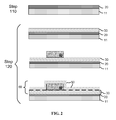
- Fig. 1 provides a flowchart of a method of manufacturing an optical device, which includes a substrate coating step 110, a loaded spacer step 120, a modifying step 130, and a third layer step 140.
- a substrate 11 is at least partially coated with a reflector layer 20.
- the substrate 11 may be coated with other layers, such as a release layer or printed ink information (not shown in Fig. 2 ).
- the release layer is a layer allowing to transfer all coatings from the foil substrate to another substrate, for example a security document or authentication document.
- a spacer layer 60 is provided onto the reflector layer 20.
- the spacer layer 60 includes a first portion of spacer material 30, a second portion of spacer material 50, and a soluble pocket 40 within the spacer layer 60; the pocket 40 is disposed between the spacer material portions 30 and 50.
- the first portion of spacer material 30 is deposited onto the reflector layer 20; then a soluble material is patterned thereon, by way of example using an ink-jet printer, so as to partially cover the spacer material 30 with a soluble pocket 40. Subsequently, the second portion of spacer material 50 is deposited so as to at least partially cover the soluble pocket 40 and the previously deposited spacer material 30. It would be appreciated that the figures are schematic representation of the embodiments and not all the details are shown. In particular, the top surface of the spacer material 50 is not flat because of the conforming effect.
- the spacer layer 60 is modified by dissolving the soluble pocket 40 in a solvent so as to remove a portion of the spacer material 45, which was deposited on top of the soluble pocket 40.
- the dissolution of the pocket 40 and removal of the spacer material 45 provides a spacer layer 65 which has a varying layer thickness illustrated in Fig. 3 as h 1 and h 2 in adjacent regions 85 and 80, respectively.
- the spacer layer 65 is coated with an absorber layer 70 so as to complete forming an interference optical filter 100.
- the absorber layer 70 may be further coated with a release layer, a protective layer, a dry adhesive layer, printed ink information, etc.
- the resulting device includes the interference optical filter 100, wherein the thickness of the spacer layer 65 varies from one region to another.
- the thicknesses h 1 and h 2 of the spacer layer 65 may be chosen so as to provide two different optical effects to an observer 90, who would observe at least two adjacent regions, marked in Fig. 3 as regions 80 and 85, with a well defined border therebetween.
- the substrate 11 may include such materials as glass, mica, alumina, iron oxide, graphite, bismuth oxychloride, boron nitride, polymer or metal or similar particle.
- the substrate 11 may be a piece of paper, cardboard, textile, foil, polymer sheet, metal.
- suitable reflector material for the reflector layer 20 preferably a metal with a reflectance of greater than 70%; suitable materials include aluminum, silver, iron, tantalum, iridium, rhenium, copper, silver, gold, platinum, palladium, nickel, cobalt, niobium, chromium, tin, and combinations or alloys.
- the reflector layer 20 may be a patterned or segmented reflector layer with windows absent the reflective material.
- Various techniques may be used to pattern the metal layer, such as chemical etching or oil ablation in vacuum.
- Suitable materials for the spacer layer 65 include zinc sulfide (ZnS), zinc oxide (ZnO), zirconium oxide (ZrO 2 ), titanium dioxide (TiO 2 ), diamond-like carbon, indium oxide (In 2 O 3 ), indium-tin-oxide ("ITO"), tantalum pentoxide (Ta 2 O 5 ), ceric oxide (CeO 2 ) yttrium oxide (Y 2 O 3 ), europium oxide (Eu 2 O 3 ), iron oxides such as (II)diiron(III) oxide (Fe 3 O 4 ) and ferric oxide (Fe 2 O 3 ), hafnium nitride (HfN), hafnium carbide (HfC), hafnium oxide (HfO 2 ), lanthanum oxide (La 2 O 3 ), magnesium oxide (MgO), neodymium oxide (Nd 2 O 3 ), praseodymium oxide (Pr 6 O 11 ), samarium
- Suitable absorber materials for the absorber layer 70 include chromium, nickel, iron, titanium, aluminum, tungsten, molybdenum, niobium, combinations, compounds or alloys thereof, such as INCONEL.TM. (Ni--Cr--Fe), metals mixed in a dielectric matrix, or other substances that are capable of acting as a uniform or selective absorber in the visible spectrum.
- the absorber can also be a dielectric material such as an iron oxide (e.g., Fe 2 O 3 ), silicon monoxide (SiO), chromium oxide (Cr 2 O 3 ), carbon, titanium sub-oxide (TiO x ) where x is less than 2.0), metal carbides, metal carbo-nitrides, combinations thereof, and the like.
- Metal absorber layers are generally deposited in a layer that is sufficiently thin so as to allow substantial transmission of light through the absorber layer.
- the thin film layers can be deposited using any conventional thin film deposition techniques.
- Nonlimiting examples of such techniques include physical vapor deposition (PVD), chemical vapor deposition (CVD), plasma enhanced (PE) variations thereof, such as PECVD or downstream PECVD, sputtering, electrolytic deposition, sol-gel, and other like deposition methods that lead to the formation of substantially uniform continuous thin film layers.
- PVD physical vapor deposition
- CVD chemical vapor deposition
- PE plasma enhanced
- the release layer may be coated using the aforementioned methods or other non vacuum processes such as gravure, wire wound bars, flexographic applications.
- the soluble pocket 40 various materials may be used which may be dissolved by the solvent used in the modifying step 130 to dissolve the pocket 40.
- watersoluble materials such as polyvinylpyrolidone
- a water-based solvent Typically this material is deposited to a thickness ranging from 0.2 to 2 mils.
- the soluble pocket 40 can be formed of other materials such a wax, acrylic polyamide, polyamide, urethane or epoxy which are dissolved in organic solvents such as methylethyl ketones, acetones, alcohol and the like.
- polymers that can be used as binders for soluble inks, paints and coatings include polyvinyl alcohol, polyvinyl acetate polyvinylpyrrolidone, poly(ethoxyethylene), poly(methoxyethylene), poly(acrylic) acid, poly(acrylamide), poly(oxyethylene), poly(maleic anhydride), hydroxyethyl cellulose, cellulose acetate, poly(sacchrides) such as gum arabic and pectin, poly(acetals), such as polyvinylbutyral, poly(vinyl halides), such as polyvinyl chloride and polyvinylene chloride, poly(dienes) such as polybutadiene, poly(alkenes) such as polyethylene, poly(acrylates) such as polymethyl acrylate, poly(methacrylates) such as poly methylmethacrylate, poly(carbonates) such as poly(oxycarbonyl oxyhexamethylene, poly(esters) such as polyethylene terephthalate, poly(urethan
- inks or coatings can be formulated to be soluble on acidic or base solutions for other possible convenient applications.
- the soluble material of the soluble pocket 40 can be applied using any printing technique, such as gravure, flexographic, offset, letterpress, laser toner, inkjet, or screen printing.
- the soluble pocket 40 is applied using a painting step, such as rolling, dipping, brushing, or spray painting.
- fingerprints or personal signatures made with a special ink may render color shifting and different from the background; a pattern can be , the soluble material can be also applied with a rubber stamp.
- Registration of the printed inks gives a large combination of different color shifting effects, transparent windows, non-color shifting background, etc.
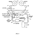
- the soluble pocket 40 may be removed using a stripping apparatus shown in Fig. 4 .
- the substrate 11 is carried by unwind and rewind reels 31 and 32.
- the flexible substrate 11 passes from the rewind reel 31 over a roller 33 and then below a roller 34 which is immersed in the solvent carried within the tank 26.
- the substrate 11 then passes from the roller 34 to the roller 36 and remains in the solvent for a sufficient period of time so that the solvent can dissolve the soluble pocket40. Thereafter, the substrate 11 passes over a roller 37 and is rewound onto the rewind reel 32.
- Means is provided for recirculating and filtering the solvent in the tank 26 and consists of piping 41 connected to the outlet from the tank 26 and connected to a circulation pump 42 which is connected by piping to the inlet of the filter 44.
- the output of the filter 44 is connected by piping 46 to the inlet of a heater 47.
- the outlet of the heater 47 is connected by piping 48 to the inlet to the tank 26.
- agitation in the form of a mechanical agitation provided by suitable means such as ultrasonic transducers 51 located in the bottom of the tank 26 can be utilized for agitating the solvent.
- a mechanical brush agitator 52 can be provided adjacent the roller 36 to engage the exposed surface of the substrate 11 to ensure that the spacer material 45 carried by the soluble pocket 40 is separated from the web or substrate 11.
- jets of the solvent can be provided when needed in the separation process. The jets can be provided by a spray nozzle 54 supplied with solvent from a high pressure pump 56 converted into the piping 48.
- the substrate Before the substrate 11 is wound onto the rewind reel 32, the substrate can be dried by suitable means such as a pair of dryers 57 disposed on opposite sides of the substrate 11 to dry the same prior to the substrate 11 travelling over the roller 37.
- optical thickness is a well known optical parameter defined as the product ⁇ d, where ⁇ is the refractive index of the layer and d is the physical thickness of the layer.
- ⁇ is the refractive index of the layer
- d is the physical thickness of the layer.
- the optical thickness of a layer is expressed in terms of a quarter wave optical thickness (QWOT) that is equal to 4 ⁇ d/ ⁇ , where ⁇ is the wavelength at which a QWOT condition occurs.
- QWOT quarter wave optical thickness
- the optical thicknesses of the dielectric spacer layer 65 can range from about 2 QWOT at a design wavelength of about 400 nm to about 9 QWOT at a design wavelength of about 700 nm, and preferably 2-6 QWOT at 400-700 nm, depending upon the color shift desired.
- the thicknesses h 1 and h 2 may be chosen so that to provide two different color shifting effects to the observer 90.
- Fig. 5 illustrates an exemplary design produced with the method described above with reference to Figs. 1-3 .
- the spacer layer is thinner in square regions 220 than in a surrounding area 210, which correspond to regions 85 and 80 of Fig. 3 , respectively.
- the squares 220 appear green at near-normal viewing conditions; the color of the squares 220 shifts to red/purple at higher viewing angles.
- the surrounding area 210 with a thicker spacer layer exhibits red/purple coloration at near-normal viewing angles; the color of the surrounding area 210 shifts to green at higher viewing angles.
- a reflector layer formed of 80 nm of Aluminum was deposited onto a PET substrate, exemplifying the reflector 20 and substrate 11 of Fig. 2 , respectively.
- an dielectric spacer material MgF 2 was deposited on the reflector layer to the thickness h 1 equal to 6QW MgF2 @ 507nm.
- the square regions 220 were printed with four different acetone soluble inks on top of the MgF 2 layer; each of the squares is an example of the soluble pocket 40 shown in Fig. 3 .
- the four acetone soluble inks were:
- the printed inks formed four square-shaped soluble pockets. Further, 75 nm of the spacer material MgF 2 were deposited onto the soluble pockets and the previously deposited spacer material, thereby forming a spacer layer on the reflector.
- the spacer layer was modified by rubbing the area with a cotton tip embedded with acetone so as to dissolve the soluble pockets and to remove portions of the spacer material deposited onto the soluble pockets.
- the result was a spacer layer having a varying layer thickness, as the spacer layer 65 in Fig. 3 .
- an absorber layer formed of 10 nm of Chromium was deposited onto the spacer layer.
- Figs. 6 and 7 provide results of an optical analysis performed with Datacolor SF600 Spectrophotometer and the a*,b* color trajectory measured with a Zeiss instrument.
- Curves 240 and 250 correspond to the square regions 220, which change in color from green to purple.
- Curves 260 and 270 correspond to the surrounding area 210, which shift in color from red to green.
- Fig. 6 shows reflectance as a function of wavelength for the two color shifting areas. The reflectance peaks correspond to greenish and reddish colors for each color shifting design.
- Fig. 7 shows color trajectories corresponding to the aforedescribed optical designs :
- thicker design A1/ 2 QW MgF 2 @577 nm/ 10 nm Cr; the thicker design differs from the thinner design by 70 nm of MgF2.
- Example 2 differs from Example 1 in that the spacer materials was chosen SiO 2 deposited to the same thicknesses as MgF 2 in Example 1. The resulting device exhibits blue-to-magenta color shifting squares and green-to-blue background.
- the substrate coating step 110 includes providing a substrate which has one or more layers deposited thereon and then coating the substrate with one of a reflector or an absorber layer.
- the additional layers may be a magnetic layer, a relief-forming layer, a release/hardcoat layer, etc.
- the release layer may be soluble with a solvent different from one used for dissolving the soluble pocket 40.
- the relief forming layer 25 is disposed on the substrate 11.
- a relief pattern 45 formed in the relief forming layer 25 underlies the interference filter 100.
- the substrate coating step 110 includes providing a substrate which has a relief forming layer with a relief pattern formed therein and then coating the substrate with one of a reflector or an absorber layer.
- the methods of forming the relief pattern 45 are known in the art and include embossing, gravure, and casting. Examples of the relief pattern include diffractive, holographic, pyramidal microstructures. The pyramidal microstructures are used for special color by rotation effects described, for example in U.S. Patent Application Pub. No. 20080286501 , incorporated herein by reference.
- the relief pattern may be a grating structure with a frequency in the range from 10 grooves/mm to 5000 grooves/mm; the gratings can be of any shape and size, symmetrical or asymmetrical, such as linear, cross, sinusoidal, triangular, square, pyramidal, to create any kind of optical effects such as reflection, diffraction, scattering ,dispersion, etc of the electromagnetic spectrum.
- the grooves could be sinusoidal, square, triangular, trapezoidal, etc.
- the relief pattern may be formed in the substrate surface or in an additional layer coated onto the substrate.
- Example 2 This example is different from the design of Example 2 in that the substrate 11 is a grated PET substrate with a 1500 ln/mm grating formed of linear sinusoidal grooves.
- the four inks described on Example 1 were tested; all of them exhibited good patterning properties and provided four squares with a thinner layer of SiO 2 surrounded by a background with a thicker layer of SiO 2 .
- the resulting sample exhibits a combination of thin film and diffractive interference. Different thicknesses of the dielectric spacer layer produce different thin film interference effects as explained above.
- the diffractive optical effect caused by the grating may be observed when the device is illuminated and viewed across the grooves; and no diffractive effect is observed when the device is viewed parallel to the grooves direction. When the device is viewed across the grooves, a combination of thin film interference and diffractive interference is observed.
- the method of this invention can be practiced when the substrate has a microstructure thereon.
- the substrate coating step 110 includes coating the substrate 11 with an absorber layer such as the absorber layer 70
- the third layer step 140 includes coating the spacer layer 65 with a reflector layer such as the reflector layer 20, as shown in Fig. 9 .
- the resulting device is different from the device 100 in that the positions of the reflector layer 20 and the absorber layer 70 are interchanged. Accordingly, the color-shifting effects are visible through the substrate 11, which is a transparent or at least light transmissible substrate in this case.
- the method illustrated in Fig. 1 may be modified to replace the reflector layer 20 with a second absorber layer so as to make the interference filter 100 to be a partially light transmissive interference filter. Accordingly, method steps 120 and 140, coating a reflector layer in one step and an absorber layer in another step, are replaced with steps 121 and 141, both coating an absorber layer.
- the materials and methods of deposition suitable for the absorber layer 70 are also suitable for the second absorber layer.
- the substrate 11 may be light transmissive so that color-shifting effects may be observed from both sides of the device. Printed text or any opaque design disposed on one side of the partially light transmissive interference filter, e.g. between the substrate 11 and the second absorber layer, would be visible through the interference filter.
- different spacer materials are used in a first portion 30 and a second portion 50 of the spacer layer 65.
- one of the spacer materials may have an index of refraction higher than 1.65, a so-called high-index material, and another material may have an index of refraction less than 1.65, a so-called low-index material.
- the first and second portions of the spacer layer 65 are formed of a same spacer material.
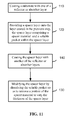
- the modifying step 130 is performed after the third layer step 140, as shown in Fig. 11 .
- the third layer step 140 results in a layered structure shown in Fig. 12 , which has the soluble pocket 40 within spacer layer 60.
- the soluble pocket 40 is dissolved and the adjacent portion of the spacer layer 45 as well as a portion of the absorber layer 145 are removed; the resulting device is shown in Fig. 13 ; to the observer 90 it provides a color shifting effect in the region 80 and a silver mirror effect in the region 85.
- a substrate is coated with Al, then with 6 QW SiO2 @507 nm. After that, four soluble square pockets are printed with soluble ink and 10 nm Cr deposited on top. Finally, the ink is dissolved and the resulting device exhibits silver squares surrounded with a green-to-purple color shifting region.
- the step of includes forming a second soluble pocket within the spacer layer, and wherein the second soluble pocket is dissolved after the third layer deposition step 140.
- the resulting device provides two different color-shifting effects and a silver mirror effect in the region of the second soluble pocket.
- the first soluble pocket 40 and the second soluble pocket may be soluble in different solvents, i.e. the first soluble pocket is soluble in a first solvent and the second soluble pocket is soluble in a second solvent and not soluble in the first solvent.
- a substrate 300 is coated with a release layer 310, an optional support layer 315 that if used could be microstructured or not, an absorber layer 320, and a spacer layer 330 which includes a dissolvable pocket 335.
- the dissolvable pocket 335 is dissolved so as to vary the thickness of the spacer layer 330.
- the resulting structure may replace the substrate 11, e.g. in the method described with reference to Figs. 2 and 3 , providing a double-sided optical structure, both sides of which exhibit two different optical effect, such as color-shifting or mirror effects.
- a pattern of soluble ink is applied onto a first side of a transparent substrate and subsequently coated with three consecutives layers of Reflector/Dielectric/Absorber, e.g. such as described in Example 1, and the soluble material is dissolved.
- a A1/ 4 QW MgF2 @530 nm/ 10 nm Cr design provides a green-blue patterned color shifting device.
- Another three-layered structure of an Absorber/Dielectric/Reftector design, e.g. such as described in Example 2 may be formed on a second side of the substrate. Alternatively, the second side may be coated with colored pigments. At the first side an observer would see two color-shifting effects corresponding to the optical designs of Examples 1 and 2.
- the substrate may be have a pyramidal microstructure formed in the surface of the substrate of in an additional relief forming layer.
- a color-shifting all dielectric stack is formed of a plurality of dielectric layers alternating layers having a high refractive index, i.e. greater than 1.65, and layers having a low index of refraction, i.e. less than 1.65.
- the layers are arranged in a (LH) n , (HLH) n , or (LHL) n , etc., design.
- the stack is patterned as described above using one or more soluble pockets in one or more layers so as to create various color-shifting effects.
- the color-shifting all dielectric stack may be formed directly on a substrate or on a reflector layer.
- the reflector layer may be a metal reflector as the reflector layer 20 described above or a dielectric mirror formed of multiple thin film layers as known in the art.
- the substrate may be microstructured as described above.
- devices manufactured in accordance with the method of this invention may be used for protection of banknotes, value papers, identification documents, access cards, credit cards, gift cards, security labels and packaging, identification plates, security threads, windows, fibers, stamps, labels, stock passports, and the like.
- the method of this invention provides high resolution and is easy to adapt to any pattern.
Abstract
Description
- The present invention relates to optical interference filters for providing a color shift effect and, more particularly, to optical filters with a dielectric spacer layer such that different regions thereof have different thicknesses.
- It is well known that interference effects provided by thin film layered coatings depend, in particular, on the thickness of the layers. Accordingly, various interference structures have been suggested where at least one layer has a varying thickness in order to modify the effect provided by the structure.
- By way of example,
U.S. Patent No. 5,009,486 in the name of Dobrowolski et al . teaches a form depicting coating with a marginal portion which decreases in thickness so as to provide a multi-colored aureole around the form. - Various methods of forming thin film layers with variations of thickness have been developed, such as masked deposition or polymerizing a monomer to different degrees for varying the shrinkage of the film and hence the thickness of the film.
- The mechanical masking technique is difficult to use in mass production and is associated with additional cost. Even for a simple pattern of continuous coated and non-coated bands, it requires a system, conventionally driven by a belt, where shadowing strips run continuously between a coating material source and a water cooled drum which supports a moving substrate to be patterned. Strips on this roller system match in width with non-coated bands on the substrate. Even this simple system presents problems when a coating material is evaporated. Over the time, the build up on the strips creates edge definition problem. Additionally, due to the high temperature, dimensions of the strips tend to change. The change in dimensions has to be compensated by a difference in the tension applied to the strips. This result in significant cost associated with the masking technique.
-
U.S. Patent No. 6,010,751 in the name of Shaw et al. teaches a dielectric layer formed by evaporating an acrylate monomer. The acrylate condenses on the substrate and is polymerized in situ for forming a monolithic film. Different areas of the film may have different thicknesses formed by using a mask between a heated drum and the film. - International application
WO2005038136 in the name of Heim et al. teaches an interference structure with a polymeric dielectric layer modified by elongation, electromagnetic radiation, electron beam treatment, pressure and/or temperature. - None of the conventional methods provides a solution that is both a cost effective and environmentally friendly.
- These methods do not provide two adjacent regions each having a predetermined thickness in accordance with the design requirements and a well defined border therebetween. By way of example, Shaw '751 describes a sample which has a star image surrounded by a halo which gradually changes its color.
- An object of the present invention is to overcome the shortcomings of the prior art and to provide a method of forming an interference filter with two adjacent regions each having a predetermined thickness.
- Accordingly, the present invention relates to a method of manufacturing an optical device, the method comprising: (a) coating a substrate with one of a reflector or an absorber layer; (b) providing a spacer layer onto the layer coated in step (a), the spacer layer comprising a spacer material and a soluble pocket within the loaded spacer layer; (c) modifying the spacer layer by dissolving the soluble pocket so as to remove a portion of the spacer material to vary the thickness of the spacer layer, and, (d) coating the spacer layer with another of the reflector or absorber layers.
- The invention also relates to a method of manufacturing an optical device, the method comprising: (a) coating a substrate with a first absorber layer; (b) providing a spacer layer onto the first absorber layer, the spacer layer comprising a spacer material and a soluble pocket within the loaded spacer layer; (c) modifying the spacer layer by dissolving the soluble pocket so as to remove a portion of the spacer material and to vary the thickness of the spacer layer; and, (d) coating the spacer layer with a second absorber layer.
- The invention will be described in greater detail with reference to the accompanying drawings which represent preferred embodiments thereof wherein:
-
Figure 1 is a flowchart of a method of manufacturing an optical device; -
Figure 2 is a diagram illustrating the method ofFig. 1 ; -
Figure 3 is a diagram illustrating the method ofFig. 1 ; -
Figure 4 is a schematic illustration of an apparatus utilized for accomplishing wet stripping; -
Figure 5 illustrates color shifting effects produced by the device of Example 1; -
Figure 6 is a plot of reflectance as a function of wavelengths of the two color shifting areas, Example 1; -
Figure 7 is a plot of color trajectories, Example 1; -
Figure 8 is a diagram illustrating one embodiment of the invention; -
Figure 9 is a diagram illustrating one embodiment of the invention; -
Figure 10 is a flowchart of one embodiment of the method of the invention; -
Figure 11 is a flowchart of one embodiment of the method of the invention; -
Figure 12 is a diagram illustrating the method ofFig. 11 ; -
Figure 13 is a diagram illustrating the method ofFig. 11 ; and, -
Figure 14 is a diagram illustrating one embodiment of the invention. -
Fig. 1 provides a flowchart of a method of manufacturing an optical device, which includes asubstrate coating step 110, a loadedspacer step 120, a modifyingstep 130, and athird layer step 140. - With reference to
Fig. 2 , during thesubstrate coating step 110, asubstrate 11 is at least partially coated with areflector layer 20. Prior to this step, thesubstrate 11 may be coated with other layers, such as a release layer or printed ink information (not shown inFig. 2 ). The release layer is a layer allowing to transfer all coatings from the foil substrate to another substrate, for example a security document or authentication document. - In the loaded
spacer step 120, aspacer layer 60 is provided onto thereflector layer 20. Thespacer layer 60 includes a first portion ofspacer material 30, a second portion ofspacer material 50, and asoluble pocket 40 within thespacer layer 60; thepocket 40 is disposed between thespacer material portions - The first portion of
spacer material 30 is deposited onto thereflector layer 20; then a soluble material is patterned thereon, by way of example using an ink-jet printer, so as to partially cover thespacer material 30 with asoluble pocket 40. Subsequently, the second portion ofspacer material 50 is deposited so as to at least partially cover thesoluble pocket 40 and the previously depositedspacer material 30. It would be appreciated that the figures are schematic representation of the embodiments and not all the details are shown. In particular, the top surface of thespacer material 50 is not flat because of the conforming effect. - With reference to
Fig. 3 , in the modifyingstep 130, thespacer layer 60 is modified by dissolving thesoluble pocket 40 in a solvent so as to remove a portion of thespacer material 45, which was deposited on top of thesoluble pocket 40. The dissolution of thepocket 40 and removal of thespacer material 45 provides aspacer layer 65 which has a varying layer thickness illustrated inFig. 3 as h1 and h2 inadjacent regions - In the
third layer step 140, thespacer layer 65 is coated with anabsorber layer 70 so as to complete forming an interferenceoptical filter 100. Theabsorber layer 70 may be further coated with a release layer, a protective layer, a dry adhesive layer, printed ink information, etc. - The resulting device includes the interference
optical filter 100, wherein the thickness of thespacer layer 65 varies from one region to another. The thicknesses h1 and h2 of thespacer layer 65 may be chosen so as to provide two different optical effects to anobserver 90, who would observe at least two adjacent regions, marked inFig. 3 asregions - The
substrate 11 may include such materials as glass, mica, alumina, iron oxide, graphite, bismuth oxychloride, boron nitride, polymer or metal or similar particle. Thesubstrate 11 may be a piece of paper, cardboard, textile, foil, polymer sheet, metal. - Examples of suitable reflector material for the
reflector layer 20 preferably a metal with a reflectance of greater than 70%; suitable materials include aluminum, silver, iron, tantalum, iridium, rhenium, copper, silver, gold, platinum, palladium, nickel, cobalt, niobium, chromium, tin, and combinations or alloys. - The
reflector layer 20 may be a patterned or segmented reflector layer with windows absent the reflective material. Various techniques may be used to pattern the metal layer, such as chemical etching or oil ablation in vacuum. - Suitable materials for the
spacer layer 65 include zinc sulfide (ZnS), zinc oxide (ZnO), zirconium oxide (ZrO2), titanium dioxide (TiO2), diamond-like carbon, indium oxide (In2O3), indium-tin-oxide ("ITO"), tantalum pentoxide (Ta2O5), ceric oxide (CeO2) yttrium oxide (Y2O3), europium oxide (Eu2O3), iron oxides such as (II)diiron(III) oxide (Fe3O4) and ferric oxide (Fe2O3), hafnium nitride (HfN), hafnium carbide (HfC), hafnium oxide (HfO2), lanthanum oxide (La2O3), magnesium oxide (MgO), neodymium oxide (Nd2O3), praseodymium oxide (Pr6O11), samarium oxide (Sm2O3), antimony trioxide (Sb2O3), silicon (Si), silicon monoxide (SiO), germanium (Ge), selenium trioxide (Se2O3), tin oxide (SnO2), tungsten trioxide (WO3), silicon dioxide (SiO2), aluminum oxide (Al2O3), metal fluorides such as magnesium fluoride (MgF2), aluminum fluoride (AlF3), cerium fluoride (CeF3), lanthanum fluoride (LaF3), sodium aluminum fluorides (e.g., Na3AlF6 or Na5Al3F14), neodymium fluoride (NdF3), samarium fluoride (SmF3), barium fluoride (BaF2), calcium fluoride (CaF2), lithium fluoride (LiF), and combinations thereof, and organic monomers and polymers including dienes or alkenes such as acrylates (e.g., methacrylate), perfluoroalkenes, polytetrafluoroethylene (e.g., TEFLON.RTM.), fluorinated ethylene propylene ("FEP"), combinations thereof, and the like. - Examples of suitable absorber materials for the
absorber layer 70 include chromium, nickel, iron, titanium, aluminum, tungsten, molybdenum, niobium, combinations, compounds or alloys thereof, such as INCONEL.TM. (Ni--Cr--Fe), metals mixed in a dielectric matrix, or other substances that are capable of acting as a uniform or selective absorber in the visible spectrum. Alternatively, the absorber can also be a dielectric material such as an iron oxide (e.g., Fe2O3), silicon monoxide (SiO), chromium oxide (Cr2O3), carbon, titanium sub-oxide (TiOx) where x is less than 2.0), metal carbides, metal carbo-nitrides, combinations thereof, and the like. Metal absorber layers are generally deposited in a layer that is sufficiently thin so as to allow substantial transmission of light through the absorber layer. - Typically, the thin film layers, such as the
reflector layer 20,spacer layer 65, andabsorber layer 70, can be deposited using any conventional thin film deposition techniques. Nonlimiting examples of such techniques include physical vapor deposition (PVD), chemical vapor deposition (CVD), plasma enhanced (PE) variations thereof, such as PECVD or downstream PECVD, sputtering, electrolytic deposition, sol-gel, and other like deposition methods that lead to the formation of substantially uniform continuous thin film layers. The release layer may be coated using the aforementioned methods or other non vacuum processes such as gravure, wire wound bars, flexographic applications. - For the
soluble pocket 40, various materials may be used which may be dissolved by the solvent used in the modifyingstep 130 to dissolve thepocket 40. By way of example, watersoluble materials, such as polyvinylpyrolidone, can be used in combination with a water-based solvent. Typically this material is deposited to a thickness ranging from 0.2 to 2 mils. Where it is desired to utilize a solvent other than water, thesoluble pocket 40 can be formed of other materials such a wax, acrylic polyamide, polyamide, urethane or epoxy which are dissolved in organic solvents such as methylethyl ketones, acetones, alcohol and the like. - Other polymers that can be used as binders for soluble inks, paints and coatings include polyvinyl alcohol, polyvinyl acetate polyvinylpyrrolidone, poly(ethoxyethylene), poly(methoxyethylene), poly(acrylic) acid, poly(acrylamide), poly(oxyethylene), poly(maleic anhydride), hydroxyethyl cellulose, cellulose acetate, poly(sacchrides) such as gum arabic and pectin, poly(acetals), such as polyvinylbutyral, poly(vinyl halides), such as polyvinyl chloride and polyvinylene chloride, poly(dienes) such as polybutadiene, poly(alkenes) such as polyethylene, poly(acrylates) such as polymethyl acrylate, poly(methacrylates) such as poly methylmethacrylate, poly(carbonates) such as poly(oxycarbonyl oxyhexamethylene, poly(esters) such as polyethylene terephthalate, poly(urethanes), poly(siloxanes), poly(suphides), poly(sulphones), poly(vinylnitriles), poly(acrylonitriles), poly(styrene), poly(phenylenes) such as poly(2,5 dihydroxy-1,4-phenyleneethylene), poly(amides), natural rubbers, formaldahyde resins and other polymers.
- In addition, other inks or coatings can be formulated to be soluble on acidic or base solutions for other possible convenient applications.
- The soluble material of the
soluble pocket 40 can be applied using any printing technique, such as gravure, flexographic, offset, letterpress, laser toner, inkjet, or screen printing. Alternatively, thesoluble pocket 40 is applied using a painting step, such as rolling, dipping, brushing, or spray painting. By way of example, fingerprints or personal signatures made with a special ink may render color shifting and different from the background; a pattern can be , the soluble material can be also applied with a rubber stamp. - Registration of the printed inks gives a large combination of different color shifting effects, transparent windows, non-color shifting background, etc.
- The
soluble pocket 40 may be removed using a stripping apparatus shown inFig. 4 . - In the stripping apparatus 24 shown in
Fig. 4 , thesubstrate 11 is carried by unwind and rewindreels flexible substrate 11 passes from therewind reel 31 over aroller 33 and then below aroller 34 which is immersed in the solvent carried within thetank 26. Thesubstrate 11 then passes from theroller 34 to theroller 36 and remains in the solvent for a sufficient period of time so that the solvent can dissolve the soluble pocket40. Thereafter, thesubstrate 11 passes over aroller 37 and is rewound onto therewind reel 32. - Means is provided for recirculating and filtering the solvent in the
tank 26 and consists of piping 41 connected to the outlet from thetank 26 and connected to acirculation pump 42 which is connected by piping to the inlet of thefilter 44. The output of thefilter 44 is connected by piping 46 to the inlet of a heater 47. The outlet of the heater 47 is connected by piping 48 to the inlet to thetank 26. Thus it can be seen that means is provided for filtering the solvent as it is recirculated. in addition, it can be seen that, if desired, the solvent can be heated to a desired temperature to facilitate the removal of the release coating. - If additional activity is required in order to remove the
soluble pocket 40, agitation in the form of a mechanical agitation provided by suitable means such asultrasonic transducers 51 located in the bottom of thetank 26 can be utilized for agitating the solvent. In addition, amechanical brush agitator 52 can be provided adjacent theroller 36 to engage the exposed surface of thesubstrate 11 to ensure that thespacer material 45 carried by thesoluble pocket 40 is separated from the web orsubstrate 11. Also jets of the solvent can be provided when needed in the separation process. The jets can be provided by aspray nozzle 54 supplied with solvent from ahigh pressure pump 56 converted into thepiping 48. Before thesubstrate 11 is wound onto therewind reel 32, the substrate can be dried by suitable means such as a pair ofdryers 57 disposed on opposite sides of thesubstrate 11 to dry the same prior to thesubstrate 11 travelling over theroller 37. - With reference to
Fig. 3 , the optical effects visible to theobserver 90 depend on the effective optical thicknesses for imparting color shifting properties to theinterference filter 100. An optical thickness is a well known optical parameter defined as the product ηd, where η is the refractive index of the layer and d is the physical thickness of the layer. Typically, the optical thickness of a layer is expressed in terms of a quarter wave optical thickness (QWOT) that is equal to 4 ηd/λ, where λ is the wavelength at which a QWOT condition occurs. The optical thicknesses of thedielectric spacer layer 65 can range from about 2 QWOT at a design wavelength of about 400 nm to about 9 QWOT at a design wavelength of about 700 nm, and preferably 2-6 QWOT at 400-700 nm, depending upon the color shift desired. The thicknesses h1 and h2 may be chosen so that to provide two different color shifting effects to theobserver 90. -
Fig. 5 illustrates an exemplary design produced with the method described above with reference toFigs. 1-3 . The spacer layer is thinner insquare regions 220 than in a surroundingarea 210, which correspond toregions Fig. 3 , respectively. Thesquares 220 appear green at near-normal viewing conditions; the color of thesquares 220 shifts to red/purple at higher viewing angles. The surroundingarea 210 with a thicker spacer layer exhibits red/purple coloration at near-normal viewing angles; the color of the surroundingarea 210 shifts to green at higher viewing angles. - To manufacture the sample shown in
Fig. 5 , a reflector layer formed of 80 nm of Aluminum was deposited onto a PET substrate, exemplifying thereflector 20 andsubstrate 11 ofFig. 2 , respectively. Then an dielectric spacer material MgF2 was deposited on the reflector layer to the thickness h1 equal to 6QW MgF2 @ 507nm. Thesquare regions 220 were printed with four different acetone soluble inks on top of the MgF2 layer; each of the squares is an example of thesoluble pocket 40 shown inFig. 3 . - The four acetone soluble inks were:
- a/ Water based film former
-
- Acrylic film former
- 65
-
- Water
- 30
-
- Amine
- To pH of 8.5 to 9.0
-
- Plasticizer
- 3.0
-
- Alcohol
- 1.0
-
- Defoamer
- 1.0
- b/ Water based non film former
-
- Acrylic non-film former
- 60
-
- Water
- 35
-
- Amine
- To pH of 8.5 to 9.0
-
- Plasticizers
- 4
-
- Defoamer
- 1
- c/ Low viscosity/low solid Water based non film former
-
- Acrylic non-film former
- 35
-
- Water
- 60
-
- Amine
- To pH of 8.5 to 9.0
-
- Plasticizers
- 4
-
- Defoamer
- 1
- d/ Solvent based film former
-
- N.P. Acetate
- 85
-
- ¼ sec RS Nitrocellulose
- 10
-
- Plasticizer
- 5
- The printed inks formed four square-shaped soluble pockets. Further, 75 nm of the spacer material MgF2 were deposited onto the soluble pockets and the previously deposited spacer material, thereby forming a spacer layer on the reflector.
- The spacer layer was modified by rubbing the area with a cotton tip embedded with acetone so as to dissolve the soluble pockets and to remove portions of the spacer material deposited onto the soluble pockets. The result was a spacer layer having a varying layer thickness, as the
spacer layer 65 inFig. 3 . After that, an absorber layer formed of 10 nm of Chromium was deposited onto the spacer layer. -
Figs. 6 and7 provide results of an optical analysis performed with Datacolor SF600 Spectrophotometer and the a*,b* color trajectory measured with a Zeiss instrument.Curves square regions 220, which change in color from green to purple.Curves area 210, which shift in color from red to green.Fig. 6 shows reflectance as a function of wavelength for the two color shifting areas. The reflectance peaks correspond to greenish and reddish colors for each color shifting design.Fig. 7 shows color trajectories corresponding to the aforedescribed optical designs : - thinner design A1/ 6 QW MgF2 @507 nm/ 10 nm Cr and
- thicker design A1/ 2 QW MgF2 @577 nm/ 10 nm Cr; the thicker design differs from the thinner design by 70 nm of MgF2.
- This example differs from Example 1 in that the spacer materials was chosen SiO2 deposited to the same thicknesses as MgF2 in Example 1. The resulting device exhibits blue-to-magenta color shifting squares and green-to-blue background.
- In one embodiment the
substrate coating step 110 includes providing a substrate which has one or more layers deposited thereon and then coating the substrate with one of a reflector or an absorber layer. The additional layers may be a magnetic layer, a relief-forming layer, a release/hardcoat layer, etc. The release layer may be soluble with a solvent different from one used for dissolving thesoluble pocket 40. - With reference to
Fig. 8 , therelief forming layer 25 is disposed on thesubstrate 11. Arelief pattern 45 formed in therelief forming layer 25 underlies theinterference filter 100. Relative to the method illustrated inFig. 1 , thesubstrate coating step 110 includes providing a substrate which has a relief forming layer with a relief pattern formed therein and then coating the substrate with one of a reflector or an absorber layer. The methods of forming therelief pattern 45 are known in the art and include embossing, gravure, and casting. Examples of the relief pattern include diffractive, holographic, pyramidal microstructures. The pyramidal microstructures are used for special color by rotation effects described, for example inU.S. Patent Application Pub. No. 20080286501 , incorporated herein by reference. The relief pattern may be a grating structure with a frequency in the range from 10 grooves/mm to 5000 grooves/mm; the gratings can be of any shape and size, symmetrical or asymmetrical, such as linear, cross, sinusoidal, triangular, square, pyramidal, to create any kind of optical effects such as reflection, diffraction, scattering ,dispersion, etc of the electromagnetic spectrum. The grooves could be sinusoidal, square, triangular, trapezoidal, etc. The relief pattern may be formed in the substrate surface or in an additional layer coated onto the substrate. - This example is different from the design of Example 2 in that the
substrate 11 is a grated PET substrate with a 1500 ln/mm grating formed of linear sinusoidal grooves. The four inks described on Example 1 were tested; all of them exhibited good patterning properties and provided four squares with a thinner layer of SiO2 surrounded by a background with a thicker layer of SiO2. The resulting sample exhibits a combination of thin film and diffractive interference. Different thicknesses of the dielectric spacer layer produce different thin film interference effects as explained above. The diffractive optical effect caused by the grating may be observed when the device is illuminated and viewed across the grooves; and no diffractive effect is observed when the device is viewed parallel to the grooves direction. When the device is viewed across the grooves, a combination of thin film interference and diffractive interference is observed..Accordingly, the method of this invention can be practiced when the substrate has a microstructure thereon. - Another embodiment of the method is similar to one described with reference to
Figs. 2 and3 with the exception that thesubstrate coating step 110 includes coating thesubstrate 11 with an absorber layer such as theabsorber layer 70, and that thethird layer step 140 includes coating thespacer layer 65 with a reflector layer such as thereflector layer 20, as shown inFig. 9 . The resulting device is different from thedevice 100 in that the positions of thereflector layer 20 and theabsorber layer 70 are interchanged. Accordingly, the color-shifting effects are visible through thesubstrate 11, which is a transparent or at least light transmissible substrate in this case. - With reference to
Fig. 10 , the method illustrated inFig. 1 may be modified to replace thereflector layer 20 with a second absorber layer so as to make theinterference filter 100 to be a partially light transmissive interference filter. Accordingly, method steps 120 and 140, coating a reflector layer in one step and an absorber layer in another step, are replaced withsteps 121 and 141, both coating an absorber layer. The materials and methods of deposition suitable for theabsorber layer 70 are also suitable for the second absorber layer. Thesubstrate 11 may be light transmissive so that color-shifting effects may be observed from both sides of the device. Printed text or any opaque design disposed on one side of the partially light transmissive interference filter, e.g. between thesubstrate 11 and the second absorber layer, would be visible through the interference filter. - In one embodiment of this invention, different spacer materials are used in a
first portion 30 and asecond portion 50 of thespacer layer 65. By way of example, one of the spacer materials may have an index of refraction higher than 1.65, a so-called high-index material, and another material may have an index of refraction less than 1.65, a so-called low-index material. In another embodiment, the first and second portions of thespacer layer 65 are formed of a same spacer material. - In one embodiment, the modifying
step 130 is performed after thethird layer step 140, as shown inFig. 11 . Thethird layer step 140 results in a layered structure shown inFig. 12 , which has thesoluble pocket 40 withinspacer layer 60. In the modifyingstep 130, thesoluble pocket 40 is dissolved and the adjacent portion of thespacer layer 45 as well as a portion of theabsorber layer 145 are removed; the resulting device is shown inFig. 13 ; to theobserver 90 it provides a color shifting effect in theregion 80 and a silver mirror effect in theregion 85. - A substrate is coated with Al, then with 6 QW SiO2 @507 nm. After that, four soluble square pockets are printed with soluble ink and 10 nm Cr deposited on top. Finally, the ink is dissolved and the resulting device exhibits silver squares surrounded with a green-to-purple color shifting region.
- In one embodiment, the step of includes forming a second soluble pocket within the spacer layer, and wherein the second soluble pocket is dissolved after the third
layer deposition step 140. The resulting device provides two different color-shifting effects and a silver mirror effect in the region of the second soluble pocket. The firstsoluble pocket 40 and the second soluble pocket may be soluble in different solvents, i.e. the first soluble pocket is soluble in a first solvent and the second soluble pocket is soluble in a second solvent and not soluble in the first solvent. - In one embodiment illustrated in
Fig. 14 , asubstrate 300 is coated with arelease layer 310, anoptional support layer 315 that if used could be microstructured or not, anabsorber layer 320, and aspacer layer 330 which includes adissolvable pocket 335. Thedissolvable pocket 335 is dissolved so as to vary the thickness of thespacer layer 330. The resulting structure may replace thesubstrate 11, e.g. in the method described with reference toFigs. 2 and3 , providing a double-sided optical structure, both sides of which exhibit two different optical effect, such as color-shifting or mirror effects. - In one embodiment, a pattern of soluble ink is applied onto a first side of a transparent substrate and subsequently coated with three consecutives layers of Reflector/Dielectric/Absorber, e.g. such as described in Example 1, and the soluble material is dissolved. By way of example, a A1/ 4 QW MgF2 @530 nm/ 10 nm Cr design provides a green-blue patterned color shifting device. Another three-layered structure of an Absorber/Dielectric/Reftector design, e.g. such as described in Example 2, may be formed on a second side of the substrate. Alternatively, the second side may be coated with colored pigments. At the first side an observer would see two color-shifting effects corresponding to the optical designs of Examples 1 and 2. Additionally, the substrate may be have a pyramidal microstructure formed in the surface of the substrate of in an additional relief forming layer.
- In one embodiment, a color-shifting all dielectric stack is formed of a plurality of dielectric layers alternating layers having a high refractive index, i.e. greater than 1.65, and layers having a low index of refraction, i.e. less than 1.65. The layers are arranged in a (LH)n, (HLH)n, or (LHL)n, etc., design. The stack is patterned as described above using one or more soluble pockets in one or more layers so as to create various color-shifting effects. The color-shifting all dielectric stack may be formed directly on a substrate or on a reflector layer. The reflector layer may be a metal reflector as the
reflector layer 20 described above or a dielectric mirror formed of multiple thin film layers as known in the art. The substrate may be microstructured as described above. - By way of example, devices manufactured in accordance with the method of this invention may be used for protection of banknotes, value papers, identification documents, access cards, credit cards, gift cards, security labels and packaging, identification plates, security threads, windows, fibers, stamps, labels, stock passports, and the like.
- Advantageously, the method of this invention provides high resolution and is easy to adapt to any pattern.
Claims (15)
- A method of manufacturing an optical device, the method comprising:(a) coating a substrate with one of a reflector or absorber layer;(b) providing a spacer layer onto the layer coated in step (a), the spacer layer comprising a spacer material and a first soluble pocket within the spacer layer;(c) modifying the spacer layer by dissolving the first soluble pocket and removing a portion of the spacer material so as to vary the thickness of the spacer layer; and,(d) coating the spacer layer with another of the reflector or absorber layers.
- A method as defined in claim 1 wherein the substrate has a release coating thereon.
- A method as defined in claim 1 wherein step (b) comprises providing a spacer material onto the layer coated in step (a), then partially covering the spacer material with the soluble pocket, then providing a spacer material onto the first soluble pocket and the previously deposited spacer material.
- A method as defined in claim 3 wherein step (b) comprises painting or printing of the soluble pocket.
- A method as defined in claim 1 wherein the substrate provided in step (a) has a relief forming layer with a relief pattern formed therein.
- A method as defined in claim 1 wherein the substrate provided in step (a) has a microstructured surface.
- A method as defined in claim 1 wherein the first soluble pocket comprises a water soluble material and wherein step (c) comprises dissolving the first soluble pocket with water.
- A method as defined in claim 1 wherein the first soluble pocket comprises an acetone soluble material and wherein step (c) comprises dissolving the first soluble pocket with acetone.
- A method as defined in claim 1 wherein the first soluble pocket comprises an alcohol soluble material and wherein step (c) comprises dissolving the first soluble pocket with alcohol.
- A method as defined in claim 1 wherein step (d) is performed after step (c).
- A method as defined in claim 1 wherein step (c) is performed after step (d).
- A method as defined in claim 1 wherein the spacer layer further comprises a second soluble pocket, wherein the first soluble pocket is soluble in a first solvent and the second soluble pocket is soluble in a second solvent and not soluble in the first solvent.
- A method of manufacturing an optical device, the method comprising:(a) coating a substrate with a first absorber layer;(b) providing a spacer layer onto the first absorber layer, the spacer layer comprising a spacer material and a soluble pocket within the spacer layer;(c) modifying the spacer layer by dissolving the soluble pocket and removing a portion of the spacer material so as to vary the thickness of the spacer layer; and,(d) coating the spacer layer with a second absorber layer.
- A method of manufacturing an optical device, the method comprising:(a) coating a substrate with a reflector layer;(b) providing a color-shifting all dielectric stack onto the reflector layer, comprising a plurality of dielectric layers, wherein at least one of the dielectric layers has a soluble pocket therein;(c) modifying the all dielectric stack by dissolving the soluble pocket.
- A method as defined in claim 14 wherein the reflector layer is a dielectric mirror.
Priority Applications (1)
| Application Number | Priority Date | Filing Date | Title |
|---|---|---|---|
| EP19203536.8A EP3644100A1 (en) | 2009-03-19 | 2010-03-16 | Patterning of a spacer layer in an interference filter |
Applications Claiming Priority (1)
| Application Number | Priority Date | Filing Date | Title |
|---|---|---|---|
| US16152009P | 2009-03-19 | 2009-03-19 |
Related Child Applications (2)
| Application Number | Title | Priority Date | Filing Date |
|---|---|---|---|
| EP19203536.8A Division-Into EP3644100A1 (en) | 2009-03-19 | 2010-03-16 | Patterning of a spacer layer in an interference filter |
| EP19203536.8A Division EP3644100A1 (en) | 2009-03-19 | 2010-03-16 | Patterning of a spacer layer in an interference filter |
Publications (2)
| Publication Number | Publication Date |
|---|---|
| EP2230539A1 true EP2230539A1 (en) | 2010-09-22 |
| EP2230539B1 EP2230539B1 (en) | 2019-12-04 |
Family
ID=42236789
Family Applications (2)
| Application Number | Title | Priority Date | Filing Date |
|---|---|---|---|
| EP19203536.8A Withdrawn EP3644100A1 (en) | 2009-03-19 | 2010-03-16 | Patterning of a spacer layer in an interference filter |
| EP10156660.2A Active EP2230539B1 (en) | 2009-03-19 | 2010-03-16 | Patterning of a spacer layer in an interference filter |
Family Applications Before (1)
| Application Number | Title | Priority Date | Filing Date |
|---|---|---|---|
| EP19203536.8A Withdrawn EP3644100A1 (en) | 2009-03-19 | 2010-03-16 | Patterning of a spacer layer in an interference filter |
Country Status (4)
| Country | Link |
|---|---|
| US (1) | US20100239753A1 (en) |
| EP (2) | EP3644100A1 (en) |
| CN (1) | CN101907732B (en) |
| HK (1) | HK1149330A1 (en) |
Cited By (1)
| Publication number | Priority date | Publication date | Assignee | Title |
|---|---|---|---|---|
| EP2873994A1 (en) * | 2013-11-18 | 2015-05-20 | JDS Uniphase Corporation | Matched interference pigments or foils and design method |
Families Citing this family (6)
| Publication number | Priority date | Publication date | Assignee | Title |
|---|---|---|---|---|
| US8815337B2 (en) * | 2011-04-21 | 2014-08-26 | Sigma Laboratories Of Arizona, Llc | Methods for fabrication of polymer-based optically variable devices |
| US20120273256A1 (en) * | 2011-04-29 | 2012-11-01 | Innovation & Infinity Global Corp. | Transparent conductive structure applied to a touch panel and method of making the same |
| EP2538247B1 (en) * | 2011-06-23 | 2018-04-11 | Viavi Solutions Inc. | Multi color-shifting security devices |
| CN104375285B (en) * | 2014-11-19 | 2016-05-25 | 东莞市莞信企业管理咨询有限公司 | A kind of anti-blue light eyeglass |
| CN104483731B (en) * | 2014-12-31 | 2017-08-29 | 深圳莱宝高科技股份有限公司 | Colored filter and preparation method thereof |
| US9947548B2 (en) * | 2016-08-09 | 2018-04-17 | International Business Machines Corporation | Self-aligned single dummy fin cut with tight pitch |
Citations (5)
| Publication number | Priority date | Publication date | Assignee | Title |
|---|---|---|---|---|
| US5009486A (en) | 1984-06-08 | 1991-04-23 | Canadian Patents And Development Limited/Societe Canadienne Des Brevets Et D'exploitation Limitee | Form depicting, optical interference authenticating device |
| US6010751A (en) | 1995-03-20 | 2000-01-04 | Delta V Technologies, Inc. | Method for forming a multicolor interference coating |
| WO2005038136A1 (en) | 2003-10-17 | 2005-04-28 | Giesecke & Devrient Gmbh | Security element with a color-shift effect |
| EP1592067A1 (en) * | 2004-01-15 | 2005-11-02 | Matsushita Electric Industries Co., Ltd. | Solid state imaging device, process for fabricating solid state imaging device and camera employing same |
| US20080286501A1 (en) | 2007-05-07 | 2008-11-20 | Jds Uniphase Corporation | Structured surfaces that exhibit color by rotation |
Family Cites Families (16)
| Publication number | Priority date | Publication date | Assignee | Title |
|---|---|---|---|---|
| US2590906A (en) * | 1946-11-22 | 1952-04-01 | Farrand Optical Co Inc | Reflection interference filter |
| US3338730A (en) * | 1964-02-18 | 1967-08-29 | Little Inc A | Method of treating reflective surfaces to make them multihued and resulting product |
| US3858977A (en) * | 1972-01-18 | 1975-01-07 | Canadian Patents Dev | Optical interference authenticating means |
| US4242378A (en) * | 1979-03-29 | 1980-12-30 | Reiko Co., Ltd. | Method of making a decorated film with a metal layer in the form of a given pattern |
| DE3715640A1 (en) * | 1987-05-11 | 1988-11-24 | Helmuth Schmoock | FILM WITH AT LEAST ONE WINDOW METALLIZED SURFACE AND METHOD AND DEVICE FOR THEIR PRODUCTION |
| US5059454A (en) * | 1989-04-26 | 1991-10-22 | Flex Products, Inc. | Method for making patterned thin film |
| US5331443A (en) * | 1992-07-31 | 1994-07-19 | Crown Roll Leaf, Inc. | Laser engraved verification hologram and associated methods |
| US6208466B1 (en) * | 1998-11-25 | 2001-03-27 | 3M Innovative Properties Company | Multilayer reflector with selective transmission |
| US6203952B1 (en) * | 1999-01-14 | 2001-03-20 | 3M Innovative Properties Company | Imaged article on polymeric substrate |
| GB0015871D0 (en) * | 2000-06-28 | 2000-08-23 | Rue De Int Ltd | A security device |
| DE10064616C2 (en) * | 2000-12-22 | 2003-02-06 | Ovd Kinegram Ag Zug | Decorative film and method for labeling the decorative film |
| US20030043464A1 (en) * | 2001-08-30 | 2003-03-06 | Dannenberg Rand David | Optical coatings and associated methods |
| US7261920B2 (en) * | 2002-04-24 | 2007-08-28 | Sipix Imaging, Inc. | Process for forming a patterned thin film structure on a substrate |
| US7224116B2 (en) * | 2002-09-11 | 2007-05-29 | Osram Opto Semiconductors Gmbh | Encapsulation of active electronic devices |
| JP3647834B2 (en) * | 2002-09-25 | 2005-05-18 | 松下電器産業株式会社 | Mirror for exposure apparatus, reflective mask for exposure apparatus, exposure apparatus and pattern forming method |
| AU2006202315B2 (en) * | 2005-06-17 | 2011-01-27 | Viavi Solutions Inc. | Covert security coating |
-
2010
- 2010-03-16 EP EP19203536.8A patent/EP3644100A1/en not_active Withdrawn
- 2010-03-16 EP EP10156660.2A patent/EP2230539B1/en active Active
- 2010-03-18 US US12/727,196 patent/US20100239753A1/en not_active Abandoned
- 2010-03-18 CN CN201010139114.6A patent/CN101907732B/en not_active Expired - Fee Related
-
2011
- 2011-04-08 HK HK11103583.4A patent/HK1149330A1/en not_active IP Right Cessation
Patent Citations (5)
| Publication number | Priority date | Publication date | Assignee | Title |
|---|---|---|---|---|
| US5009486A (en) | 1984-06-08 | 1991-04-23 | Canadian Patents And Development Limited/Societe Canadienne Des Brevets Et D'exploitation Limitee | Form depicting, optical interference authenticating device |
| US6010751A (en) | 1995-03-20 | 2000-01-04 | Delta V Technologies, Inc. | Method for forming a multicolor interference coating |
| WO2005038136A1 (en) | 2003-10-17 | 2005-04-28 | Giesecke & Devrient Gmbh | Security element with a color-shift effect |
| EP1592067A1 (en) * | 2004-01-15 | 2005-11-02 | Matsushita Electric Industries Co., Ltd. | Solid state imaging device, process for fabricating solid state imaging device and camera employing same |
| US20080286501A1 (en) | 2007-05-07 | 2008-11-20 | Jds Uniphase Corporation | Structured surfaces that exhibit color by rotation |
Cited By (6)
| Publication number | Priority date | Publication date | Assignee | Title |
|---|---|---|---|---|
| EP2873994A1 (en) * | 2013-11-18 | 2015-05-20 | JDS Uniphase Corporation | Matched interference pigments or foils and design method |
| CN104656175A (en) * | 2013-11-18 | 2015-05-27 | Jds尤尼弗思公司 | Matched interference pigments or foils and design method thereof |
| US10061065B2 (en) | 2013-11-18 | 2018-08-28 | Viavi Solutions Inc. | Interference pigments or foils as separate structures having color match or mismatch depending on viewing angle |
| EP3561557A1 (en) * | 2013-11-18 | 2019-10-30 | Viavi Solutions Inc. | Matched interference pigments or foils and design methods |
| CN104656175B (en) * | 2013-11-18 | 2020-04-03 | 唯亚威通讯技术有限公司 | Matched interference pigments or foils and methods of designing same |
| US11079525B2 (en) | 2013-11-18 | 2021-08-03 | Viavi Solutions Inc. | Matched interference pigments or foils having viewing angle dependent mismatch |
Also Published As
| Publication number | Publication date |
|---|---|
| CN101907732B (en) | 2015-08-19 |
| US20100239753A1 (en) | 2010-09-23 |
| EP2230539B1 (en) | 2019-12-04 |
| EP3644100A1 (en) | 2020-04-29 |
| CN101907732A (en) | 2010-12-08 |
| HK1149330A1 (en) | 2011-09-30 |
Similar Documents
| Publication | Publication Date | Title |
|---|---|---|
| EP2230539B1 (en) | Patterning of a spacer layer in an interference filter | |
| EP2024447B1 (en) | Matrix comprising zero-order diffractive pigments | |
| CN106660385B (en) | Light metamagnetism safety line and item | |
| US7645510B2 (en) | Provision of frames or borders around opaque flakes for covert security applications | |
| CN101636276B (en) | Safety elements, manufacturing method and application thereof, and data mediums equiped thereon | |
| DK2417207T3 (en) | READY MAGNETIC gravure ink | |
| EP1878773B1 (en) | Alignable diffractive pigment flakes | |
| EP3079916B1 (en) | Optically variable security threads and stripes and process for making such threads and stripes | |
| US20060263539A1 (en) | Alignable Diffractive Pigment Flakes And Method And Apparatus For Alignment And Images Formed Therefrom | |
| EP3561557A1 (en) | Matched interference pigments or foils and design methods | |
| EP1760118A2 (en) | Alignable diffractive pigment flakes and method for their alignment | |
| US20080024866A1 (en) | Zero-order diffractive filter | |
| CN110832110A (en) | Method for producing a metal nanoparticle layer and use thereof in decorative or security elements | |
| US20110317268A1 (en) | Zero-order diffractive pigments | |
| CN101388164A (en) | Structured surfaces that exhibit color by rotation | |
| CA3169081A1 (en) | Flat security element with optical security features | |
| WO2022100462A1 (en) | Optical anti-counterfeiting element, manufacturing method therefor, and anti-counterfeiting product | |
| EP2067825A2 (en) | Reinforced glitter |
Legal Events
| Date | Code | Title | Description |
|---|---|---|---|
| PUAI | Public reference made under article 153(3) epc to a published international application that has entered the european phase |
Free format text: ORIGINAL CODE: 0009012 |
|
| AK | Designated contracting states |
Kind code of ref document: A1 Designated state(s): AT BE BG CH CY CZ DE DK EE ES FI FR GB GR HR HU IE IS IT LI LT LU LV MC MK MT NL NO PL PT RO SE SI SK SM TR |
|
| AX | Request for extension of the european patent |
Extension state: AL BA ME RS |
|
| 17P | Request for examination filed |
Effective date: 20110322 |
|
| RAP1 | Party data changed (applicant data changed or rights of an application transferred) |
Owner name: VIAVI SOLUTIONS INC. |
|
| STAA | Information on the status of an ep patent application or granted ep patent |
Free format text: STATUS: EXAMINATION IS IN PROGRESS |
|
| 17Q | First examination report despatched |
Effective date: 20170221 |
|
| RAP1 | Party data changed (applicant data changed or rights of an application transferred) |
Owner name: VIAVI SOLUTIONS INC. |
|
| GRAP | Despatch of communication of intention to grant a patent |
Free format text: ORIGINAL CODE: EPIDOSNIGR1 |
|
| STAA | Information on the status of an ep patent application or granted ep patent |
Free format text: STATUS: GRANT OF PATENT IS INTENDED |
|
| INTG | Intention to grant announced |
Effective date: 20190702 |
|
| RIN1 | Information on inventor provided before grant (corrected) |
Inventor name: THORAVAL, CAROLE Inventor name: LADEN, PATRICK Inventor name: ARGOITIA, ALBERTO |
|
| GRAS | Grant fee paid |
Free format text: ORIGINAL CODE: EPIDOSNIGR3 |
|
| GRAA | (expected) grant |
Free format text: ORIGINAL CODE: 0009210 |
|
| STAA | Information on the status of an ep patent application or granted ep patent |
Free format text: STATUS: THE PATENT HAS BEEN GRANTED |
|
| AK | Designated contracting states |
Kind code of ref document: B1 Designated state(s): AT BE BG CH CY CZ DE DK EE ES FI FR GB GR HR HU IE IS IT LI LT LU LV MC MK MT NL NO PL PT RO SE SI SK SM TR |
|
| REG | Reference to a national code |
Ref country code: GB Ref legal event code: FG4D |
|
| REG | Reference to a national code |
Ref country code: CH Ref legal event code: EP |
|
| REG | Reference to a national code |
Ref country code: AT Ref legal event code: REF Ref document number: 1210096 Country of ref document: AT Kind code of ref document: T Effective date: 20191215 |
|
| REG | Reference to a national code |
Ref country code: DE Ref legal event code: R096 Ref document number: 602010062216 Country of ref document: DE |
|
| REG | Reference to a national code |
Ref country code: IE Ref legal event code: FG4D |
|
| REG | Reference to a national code |
Ref country code: CH Ref legal event code: NV Representative=s name: MURGITROYD AND COMPANY, CH |
|
| REG | Reference to a national code |
Ref country code: NL Ref legal event code: MP Effective date: 20191204 |
|
| REG | Reference to a national code |
Ref country code: LT Ref legal event code: MG4D |
|
| PG25 | Lapsed in a contracting state [announced via postgrant information from national office to epo] |
Ref country code: SE Free format text: LAPSE BECAUSE OF FAILURE TO SUBMIT A TRANSLATION OF THE DESCRIPTION OR TO PAY THE FEE WITHIN THE PRESCRIBED TIME-LIMIT Effective date: 20191204 Ref country code: LV Free format text: LAPSE BECAUSE OF FAILURE TO SUBMIT A TRANSLATION OF THE DESCRIPTION OR TO PAY THE FEE WITHIN THE PRESCRIBED TIME-LIMIT Effective date: 20191204 Ref country code: ES Free format text: LAPSE BECAUSE OF FAILURE TO SUBMIT A TRANSLATION OF THE DESCRIPTION OR TO PAY THE FEE WITHIN THE PRESCRIBED TIME-LIMIT Effective date: 20191204 Ref country code: LT Free format text: LAPSE BECAUSE OF FAILURE TO SUBMIT A TRANSLATION OF THE DESCRIPTION OR TO PAY THE FEE WITHIN THE PRESCRIBED TIME-LIMIT Effective date: 20191204 Ref country code: GR Free format text: LAPSE BECAUSE OF FAILURE TO SUBMIT A TRANSLATION OF THE DESCRIPTION OR TO PAY THE FEE WITHIN THE PRESCRIBED TIME-LIMIT Effective date: 20200305 Ref country code: NO Free format text: LAPSE BECAUSE OF FAILURE TO SUBMIT A TRANSLATION OF THE DESCRIPTION OR TO PAY THE FEE WITHIN THE PRESCRIBED TIME-LIMIT Effective date: 20200304 Ref country code: FI Free format text: LAPSE BECAUSE OF FAILURE TO SUBMIT A TRANSLATION OF THE DESCRIPTION OR TO PAY THE FEE WITHIN THE PRESCRIBED TIME-LIMIT Effective date: 20191204 Ref country code: BG Free format text: LAPSE BECAUSE OF FAILURE TO SUBMIT A TRANSLATION OF THE DESCRIPTION OR TO PAY THE FEE WITHIN THE PRESCRIBED TIME-LIMIT Effective date: 20200304 |
|
| PGFP | Annual fee paid to national office [announced via postgrant information from national office to epo] |
Ref country code: GB Payment date: 20200331 Year of fee payment: 11 Ref country code: DE Payment date: 20200326 Year of fee payment: 11 Ref country code: IE Payment date: 20200326 Year of fee payment: 11 |
|
| PG25 | Lapsed in a contracting state [announced via postgrant information from national office to epo] |
Ref country code: HR Free format text: LAPSE BECAUSE OF FAILURE TO SUBMIT A TRANSLATION OF THE DESCRIPTION OR TO PAY THE FEE WITHIN THE PRESCRIBED TIME-LIMIT Effective date: 20191204 |
|
| PGFP | Annual fee paid to national office [announced via postgrant information from national office to epo] |
Ref country code: CH Payment date: 20200327 Year of fee payment: 11 |
|
| PGFP | Annual fee paid to national office [announced via postgrant information from national office to epo] |
Ref country code: FR Payment date: 20200325 Year of fee payment: 11 Ref country code: MT Payment date: 20200228 Year of fee payment: 11 |
|
| PG25 | Lapsed in a contracting state [announced via postgrant information from national office to epo] |
Ref country code: RO Free format text: LAPSE BECAUSE OF FAILURE TO SUBMIT A TRANSLATION OF THE DESCRIPTION OR TO PAY THE FEE WITHIN THE PRESCRIBED TIME-LIMIT Effective date: 20191204 Ref country code: CZ Free format text: LAPSE BECAUSE OF FAILURE TO SUBMIT A TRANSLATION OF THE DESCRIPTION OR TO PAY THE FEE WITHIN THE PRESCRIBED TIME-LIMIT Effective date: 20191204 Ref country code: NL Free format text: LAPSE BECAUSE OF FAILURE TO SUBMIT A TRANSLATION OF THE DESCRIPTION OR TO PAY THE FEE WITHIN THE PRESCRIBED TIME-LIMIT Effective date: 20191204 Ref country code: PT Free format text: LAPSE BECAUSE OF FAILURE TO SUBMIT A TRANSLATION OF THE DESCRIPTION OR TO PAY THE FEE WITHIN THE PRESCRIBED TIME-LIMIT Effective date: 20200429 Ref country code: EE Free format text: LAPSE BECAUSE OF FAILURE TO SUBMIT A TRANSLATION OF THE DESCRIPTION OR TO PAY THE FEE WITHIN THE PRESCRIBED TIME-LIMIT Effective date: 20191204 |
|
| PG25 | Lapsed in a contracting state [announced via postgrant information from national office to epo] |
Ref country code: IS Free format text: LAPSE BECAUSE OF FAILURE TO SUBMIT A TRANSLATION OF THE DESCRIPTION OR TO PAY THE FEE WITHIN THE PRESCRIBED TIME-LIMIT Effective date: 20200404 Ref country code: SK Free format text: LAPSE BECAUSE OF FAILURE TO SUBMIT A TRANSLATION OF THE DESCRIPTION OR TO PAY THE FEE WITHIN THE PRESCRIBED TIME-LIMIT Effective date: 20191204 Ref country code: SM Free format text: LAPSE BECAUSE OF FAILURE TO SUBMIT A TRANSLATION OF THE DESCRIPTION OR TO PAY THE FEE WITHIN THE PRESCRIBED TIME-LIMIT Effective date: 20191204 |
|
| REG | Reference to a national code |
Ref country code: DE Ref legal event code: R097 Ref document number: 602010062216 Country of ref document: DE |
|
| REG | Reference to a national code |
Ref country code: AT Ref legal event code: MK05 Ref document number: 1210096 Country of ref document: AT Kind code of ref document: T Effective date: 20191204 |
|
| PLBE | No opposition filed within time limit |
Free format text: ORIGINAL CODE: 0009261 |
|
| STAA | Information on the status of an ep patent application or granted ep patent |
Free format text: STATUS: NO OPPOSITION FILED WITHIN TIME LIMIT |
|
| PG25 | Lapsed in a contracting state [announced via postgrant information from national office to epo] |
Ref country code: MC Free format text: LAPSE BECAUSE OF FAILURE TO SUBMIT A TRANSLATION OF THE DESCRIPTION OR TO PAY THE FEE WITHIN THE PRESCRIBED TIME-LIMIT Effective date: 20191204 Ref country code: DK Free format text: LAPSE BECAUSE OF FAILURE TO SUBMIT A TRANSLATION OF THE DESCRIPTION OR TO PAY THE FEE WITHIN THE PRESCRIBED TIME-LIMIT Effective date: 20191204 |
|
| 26N | No opposition filed |
Effective date: 20200907 |
|
| PG25 | Lapsed in a contracting state [announced via postgrant information from national office to epo] |
Ref country code: SI Free format text: LAPSE BECAUSE OF FAILURE TO SUBMIT A TRANSLATION OF THE DESCRIPTION OR TO PAY THE FEE WITHIN THE PRESCRIBED TIME-LIMIT Effective date: 20191204 Ref country code: PL Free format text: LAPSE BECAUSE OF FAILURE TO SUBMIT A TRANSLATION OF THE DESCRIPTION OR TO PAY THE FEE WITHIN THE PRESCRIBED TIME-LIMIT Effective date: 20191204 Ref country code: AT Free format text: LAPSE BECAUSE OF FAILURE TO SUBMIT A TRANSLATION OF THE DESCRIPTION OR TO PAY THE FEE WITHIN THE PRESCRIBED TIME-LIMIT Effective date: 20191204 |
|
| REG | Reference to a national code |
Ref country code: BE Ref legal event code: MM Effective date: 20200331 |
|
| PG25 | Lapsed in a contracting state [announced via postgrant information from national office to epo] |
Ref country code: LU Free format text: LAPSE BECAUSE OF NON-PAYMENT OF DUE FEES Effective date: 20200316 |
|
| PG25 | Lapsed in a contracting state [announced via postgrant information from national office to epo] |
Ref country code: IT Free format text: LAPSE BECAUSE OF FAILURE TO SUBMIT A TRANSLATION OF THE DESCRIPTION OR TO PAY THE FEE WITHIN THE PRESCRIBED TIME-LIMIT Effective date: 20191204 |
|
| PG25 | Lapsed in a contracting state [announced via postgrant information from national office to epo] |
Ref country code: BE Free format text: LAPSE BECAUSE OF NON-PAYMENT OF DUE FEES Effective date: 20200331 |
|
| REG | Reference to a national code |
Ref country code: DE Ref legal event code: R119 Ref document number: 602010062216 Country of ref document: DE |
|
| REG | Reference to a national code |
Ref country code: CH Ref legal event code: PL |
|
| GBPC | Gb: european patent ceased through non-payment of renewal fee |
Effective date: 20210316 |
|
| PG25 | Lapsed in a contracting state [announced via postgrant information from national office to epo] |
Ref country code: CH Free format text: LAPSE BECAUSE OF NON-PAYMENT OF DUE FEES Effective date: 20210331 Ref country code: LI Free format text: LAPSE BECAUSE OF NON-PAYMENT OF DUE FEES Effective date: 20210331 Ref country code: DE Free format text: LAPSE BECAUSE OF NON-PAYMENT OF DUE FEES Effective date: 20211001 Ref country code: FR Free format text: LAPSE BECAUSE OF NON-PAYMENT OF DUE FEES Effective date: 20210331 Ref country code: GB Free format text: LAPSE BECAUSE OF NON-PAYMENT OF DUE FEES Effective date: 20210316 Ref country code: IE Free format text: LAPSE BECAUSE OF NON-PAYMENT OF DUE FEES Effective date: 20210316 |
|
| PG25 | Lapsed in a contracting state [announced via postgrant information from national office to epo] |
Ref country code: TR Free format text: LAPSE BECAUSE OF FAILURE TO SUBMIT A TRANSLATION OF THE DESCRIPTION OR TO PAY THE FEE WITHIN THE PRESCRIBED TIME-LIMIT Effective date: 20191204 Ref country code: CY Free format text: LAPSE BECAUSE OF FAILURE TO SUBMIT A TRANSLATION OF THE DESCRIPTION OR TO PAY THE FEE WITHIN THE PRESCRIBED TIME-LIMIT Effective date: 20191204 |
|
| PG25 | Lapsed in a contracting state [announced via postgrant information from national office to epo] |
Ref country code: MT Free format text: LAPSE BECAUSE OF NON-PAYMENT OF DUE FEES Effective date: 20210316 Ref country code: MK Free format text: LAPSE BECAUSE OF FAILURE TO SUBMIT A TRANSLATION OF THE DESCRIPTION OR TO PAY THE FEE WITHIN THE PRESCRIBED TIME-LIMIT Effective date: 20191204 |
|
| P01 | Opt-out of the competence of the unified patent court (upc) registered |
Effective date: 20230530 |