EP2251182A2 - Method for bonding plastic micro chip - Google Patents
Method for bonding plastic micro chip Download PDFInfo
- Publication number
- EP2251182A2 EP2251182A2 EP20100006339 EP10006339A EP2251182A2 EP 2251182 A2 EP2251182 A2 EP 2251182A2 EP 20100006339 EP20100006339 EP 20100006339 EP 10006339 A EP10006339 A EP 10006339A EP 2251182 A2 EP2251182 A2 EP 2251182A2
- Authority
- EP
- European Patent Office
- Prior art keywords
- substrate
- micro chip
- organic solvent
- plastic micro
- sample
- Prior art date
- Legal status (The legal status is an assumption and is not a legal conclusion. Google has not performed a legal analysis and makes no representation as to the accuracy of the status listed.)
- Granted
Links
- 229920003023 plastic Polymers 0.000 title claims abstract description 57
- 239000004033 plastic Substances 0.000 title claims abstract description 57
- 238000000034 method Methods 0.000 title claims abstract description 36
- 239000000758 substrate Substances 0.000 claims abstract description 107
- 239000003960 organic solvent Substances 0.000 claims abstract description 38
- 238000004519 manufacturing process Methods 0.000 claims abstract description 16
- CSCPPACGZOOCGX-UHFFFAOYSA-N Acetone Chemical compound CC(C)=O CSCPPACGZOOCGX-UHFFFAOYSA-N 0.000 claims description 16
- -1 cyanoacrylate compound Chemical class 0.000 claims description 14
- YMWUJEATGCHHMB-UHFFFAOYSA-N Dichloromethane Chemical compound ClCCl YMWUJEATGCHHMB-UHFFFAOYSA-N 0.000 claims description 12
- HEDRZPFGACZZDS-UHFFFAOYSA-N Chloroform Chemical compound ClC(Cl)Cl HEDRZPFGACZZDS-UHFFFAOYSA-N 0.000 claims description 8
- VZGDMQKNWNREIO-UHFFFAOYSA-N tetrachloromethane Chemical compound ClC(Cl)(Cl)Cl VZGDMQKNWNREIO-UHFFFAOYSA-N 0.000 claims description 8
- 150000004945 aromatic hydrocarbons Chemical class 0.000 claims description 4
- FGBJXOREULPLGL-UHFFFAOYSA-N ethyl cyanoacrylate Chemical compound CCOC(=O)C(=C)C#N FGBJXOREULPLGL-UHFFFAOYSA-N 0.000 claims description 4
- 229940053009 ethyl cyanoacrylate Drugs 0.000 claims description 4
- 150000008282 halocarbons Chemical class 0.000 claims description 4
- 150000002576 ketones Chemical class 0.000 claims description 4
- 229920001651 Cyanoacrylate Polymers 0.000 claims description 3
- 238000002032 lab-on-a-chip Methods 0.000 description 6
- 239000004698 Polyethylene Substances 0.000 description 5
- 229920003229 poly(methyl methacrylate) Polymers 0.000 description 5
- 229920000573 polyethylene Polymers 0.000 description 5
- 239000004926 polymethyl methacrylate Substances 0.000 description 5
- 239000004743 Polypropylene Substances 0.000 description 4
- 239000004793 Polystyrene Substances 0.000 description 4
- 239000000463 material Substances 0.000 description 4
- 239000004417 polycarbonate Substances 0.000 description 4
- 229920000515 polycarbonate Polymers 0.000 description 4
- 229920001155 polypropylene Polymers 0.000 description 4
- 238000009832 plasma treatment Methods 0.000 description 3
- 229920000139 polyethylene terephthalate Polymers 0.000 description 3
- 239000005020 polyethylene terephthalate Substances 0.000 description 3
- 229920002223 polystyrene Polymers 0.000 description 3
- 239000000853 adhesive Substances 0.000 description 2
- 230000001070 adhesive effect Effects 0.000 description 2
- 238000003851 corona treatment Methods 0.000 description 2
- 238000007599 discharging Methods 0.000 description 2
- 239000000203 mixture Substances 0.000 description 2
- 230000003287 optical effect Effects 0.000 description 2
- 239000002904 solvent Substances 0.000 description 2
- 102000004190 Enzymes Human genes 0.000 description 1
- 108090000790 Enzymes Proteins 0.000 description 1
- 150000001299 aldehydes Chemical class 0.000 description 1
- 125000003277 amino group Chemical group 0.000 description 1
- 239000000427 antigen Substances 0.000 description 1
- 102000036639 antigens Human genes 0.000 description 1
- 108091007433 antigens Proteins 0.000 description 1
- 125000003178 carboxy group Chemical group [H]OC(*)=O 0.000 description 1
- 239000003153 chemical reaction reagent Substances 0.000 description 1
- 150000001875 compounds Chemical class 0.000 description 1
- 238000003745 diagnosis Methods 0.000 description 1
- 201000010099 disease Diseases 0.000 description 1
- 208000037265 diseases, disorders, signs and symptoms Diseases 0.000 description 1
- 238000005516 engineering process Methods 0.000 description 1
- 125000000524 functional group Chemical group 0.000 description 1
- 230000005660 hydrophilic surface Effects 0.000 description 1
- 239000012535 impurity Substances 0.000 description 1
- 230000001788 irregular Effects 0.000 description 1
- 239000000155 melt Substances 0.000 description 1
- 102000004169 proteins and genes Human genes 0.000 description 1
- 108090000623 proteins and genes Proteins 0.000 description 1
- 238000011160 research Methods 0.000 description 1
- 238000007789 sealing Methods 0.000 description 1
- 238000004381 surface treatment Methods 0.000 description 1
- 239000012756 surface treatment agent Substances 0.000 description 1
Images


Classifications
-
- B—PERFORMING OPERATIONS; TRANSPORTING
- B29—WORKING OF PLASTICS; WORKING OF SUBSTANCES IN A PLASTIC STATE IN GENERAL
- B29C—SHAPING OR JOINING OF PLASTICS; SHAPING OF MATERIAL IN A PLASTIC STATE, NOT OTHERWISE PROVIDED FOR; AFTER-TREATMENT OF THE SHAPED PRODUCTS, e.g. REPAIRING
- B29C65/00—Joining or sealing of preformed parts, e.g. welding of plastics materials; Apparatus therefor
- B29C65/48—Joining or sealing of preformed parts, e.g. welding of plastics materials; Apparatus therefor using adhesives, i.e. using supplementary joining material; solvent bonding
- B29C65/4895—Solvent bonding, i.e. the surfaces of the parts to be joined being treated with solvents, swelling or softening agents, without adhesives
-
- G—PHYSICS
- G01—MEASURING; TESTING
- G01N—INVESTIGATING OR ANALYSING MATERIALS BY DETERMINING THEIR CHEMICAL OR PHYSICAL PROPERTIES
- G01N33/00—Investigating or analysing materials by specific methods not covered by groups G01N1/00 - G01N31/00
- G01N33/48—Biological material, e.g. blood, urine; Haemocytometers
- G01N33/50—Chemical analysis of biological material, e.g. blood, urine; Testing involving biospecific ligand binding methods; Immunological testing
- G01N33/53—Immunoassay; Biospecific binding assay; Materials therefor
-
- B—PERFORMING OPERATIONS; TRANSPORTING
- B01—PHYSICAL OR CHEMICAL PROCESSES OR APPARATUS IN GENERAL
- B01L—CHEMICAL OR PHYSICAL LABORATORY APPARATUS FOR GENERAL USE
- B01L3/00—Containers or dishes for laboratory use, e.g. laboratory glassware; Droppers
- B01L3/50—Containers for the purpose of retaining a material to be analysed, e.g. test tubes
- B01L3/502—Containers for the purpose of retaining a material to be analysed, e.g. test tubes with fluid transport, e.g. in multi-compartment structures
- B01L3/5027—Containers for the purpose of retaining a material to be analysed, e.g. test tubes with fluid transport, e.g. in multi-compartment structures by integrated microfluidic structures, i.e. dimensions of channels and chambers are such that surface tension forces are important, e.g. lab-on-a-chip
- B01L3/502707—Containers for the purpose of retaining a material to be analysed, e.g. test tubes with fluid transport, e.g. in multi-compartment structures by integrated microfluidic structures, i.e. dimensions of channels and chambers are such that surface tension forces are important, e.g. lab-on-a-chip characterised by the manufacture of the container or its components
-
- B—PERFORMING OPERATIONS; TRANSPORTING
- B29—WORKING OF PLASTICS; WORKING OF SUBSTANCES IN A PLASTIC STATE IN GENERAL
- B29C—SHAPING OR JOINING OF PLASTICS; SHAPING OF MATERIAL IN A PLASTIC STATE, NOT OTHERWISE PROVIDED FOR; AFTER-TREATMENT OF THE SHAPED PRODUCTS, e.g. REPAIRING
- B29C65/00—Joining or sealing of preformed parts, e.g. welding of plastics materials; Apparatus therefor
- B29C65/02—Joining or sealing of preformed parts, e.g. welding of plastics materials; Apparatus therefor by heating, with or without pressure
- B29C65/08—Joining or sealing of preformed parts, e.g. welding of plastics materials; Apparatus therefor by heating, with or without pressure using ultrasonic vibrations
-
- B—PERFORMING OPERATIONS; TRANSPORTING
- B29—WORKING OF PLASTICS; WORKING OF SUBSTANCES IN A PLASTIC STATE IN GENERAL
- B29C—SHAPING OR JOINING OF PLASTICS; SHAPING OF MATERIAL IN A PLASTIC STATE, NOT OTHERWISE PROVIDED FOR; AFTER-TREATMENT OF THE SHAPED PRODUCTS, e.g. REPAIRING
- B29C65/00—Joining or sealing of preformed parts, e.g. welding of plastics materials; Apparatus therefor
- B29C65/48—Joining or sealing of preformed parts, e.g. welding of plastics materials; Apparatus therefor using adhesives, i.e. using supplementary joining material; solvent bonding
- B29C65/52—Joining or sealing of preformed parts, e.g. welding of plastics materials; Apparatus therefor using adhesives, i.e. using supplementary joining material; solvent bonding characterised by the way of applying the adhesive
- B29C65/54—Joining or sealing of preformed parts, e.g. welding of plastics materials; Apparatus therefor using adhesives, i.e. using supplementary joining material; solvent bonding characterised by the way of applying the adhesive between pre-assembled parts
- B29C65/548—Joining or sealing of preformed parts, e.g. welding of plastics materials; Apparatus therefor using adhesives, i.e. using supplementary joining material; solvent bonding characterised by the way of applying the adhesive between pre-assembled parts by capillarity
-
- B—PERFORMING OPERATIONS; TRANSPORTING
- B29—WORKING OF PLASTICS; WORKING OF SUBSTANCES IN A PLASTIC STATE IN GENERAL
- B29C—SHAPING OR JOINING OF PLASTICS; SHAPING OF MATERIAL IN A PLASTIC STATE, NOT OTHERWISE PROVIDED FOR; AFTER-TREATMENT OF THE SHAPED PRODUCTS, e.g. REPAIRING
- B29C66/00—General aspects of processes or apparatus for joining preformed parts
- B29C66/01—General aspects dealing with the joint area or with the area to be joined
- B29C66/02—Preparation of the material, in the area to be joined, prior to joining or welding
- B29C66/028—Non-mechanical surface pre-treatments, i.e. by flame treatment, electric discharge treatment, plasma treatment, wave energy or particle radiation
-
- B—PERFORMING OPERATIONS; TRANSPORTING
- B29—WORKING OF PLASTICS; WORKING OF SUBSTANCES IN A PLASTIC STATE IN GENERAL
- B29C—SHAPING OR JOINING OF PLASTICS; SHAPING OF MATERIAL IN A PLASTIC STATE, NOT OTHERWISE PROVIDED FOR; AFTER-TREATMENT OF THE SHAPED PRODUCTS, e.g. REPAIRING
- B29C66/00—General aspects of processes or apparatus for joining preformed parts
- B29C66/01—General aspects dealing with the joint area or with the area to be joined
- B29C66/05—Particular design of joint configurations
- B29C66/10—Particular design of joint configurations particular design of the joint cross-sections
- B29C66/11—Joint cross-sections comprising a single joint-segment, i.e. one of the parts to be joined comprising a single joint-segment in the joint cross-section
- B29C66/112—Single lapped joints
- B29C66/1122—Single lap to lap joints, i.e. overlap joints
-
- B—PERFORMING OPERATIONS; TRANSPORTING
- B29—WORKING OF PLASTICS; WORKING OF SUBSTANCES IN A PLASTIC STATE IN GENERAL
- B29C—SHAPING OR JOINING OF PLASTICS; SHAPING OF MATERIAL IN A PLASTIC STATE, NOT OTHERWISE PROVIDED FOR; AFTER-TREATMENT OF THE SHAPED PRODUCTS, e.g. REPAIRING
- B29C66/00—General aspects of processes or apparatus for joining preformed parts
- B29C66/01—General aspects dealing with the joint area or with the area to be joined
- B29C66/05—Particular design of joint configurations
- B29C66/302—Particular design of joint configurations the area to be joined comprising melt initiators
- B29C66/3022—Particular design of joint configurations the area to be joined comprising melt initiators said melt initiators being integral with at least one of the parts to be joined
-
- B—PERFORMING OPERATIONS; TRANSPORTING
- B29—WORKING OF PLASTICS; WORKING OF SUBSTANCES IN A PLASTIC STATE IN GENERAL
- B29C—SHAPING OR JOINING OF PLASTICS; SHAPING OF MATERIAL IN A PLASTIC STATE, NOT OTHERWISE PROVIDED FOR; AFTER-TREATMENT OF THE SHAPED PRODUCTS, e.g. REPAIRING
- B29C66/00—General aspects of processes or apparatus for joining preformed parts
- B29C66/50—General aspects of joining tubular articles; General aspects of joining long products, i.e. bars or profiled elements; General aspects of joining single elements to tubular articles, hollow articles or bars; General aspects of joining several hollow-preforms to form hollow or tubular articles
- B29C66/51—Joining tubular articles, profiled elements or bars; Joining single elements to tubular articles, hollow articles or bars; Joining several hollow-preforms to form hollow or tubular articles
- B29C66/53—Joining single elements to tubular articles, hollow articles or bars
- B29C66/534—Joining single elements to open ends of tubular or hollow articles or to the ends of bars
- B29C66/5346—Joining single elements to open ends of tubular or hollow articles or to the ends of bars said single elements being substantially flat
- B29C66/53461—Joining single elements to open ends of tubular or hollow articles or to the ends of bars said single elements being substantially flat joining substantially flat covers and/or substantially flat bottoms to open ends of container bodies
-
- B—PERFORMING OPERATIONS; TRANSPORTING
- B29—WORKING OF PLASTICS; WORKING OF SUBSTANCES IN A PLASTIC STATE IN GENERAL
- B29C—SHAPING OR JOINING OF PLASTICS; SHAPING OF MATERIAL IN A PLASTIC STATE, NOT OTHERWISE PROVIDED FOR; AFTER-TREATMENT OF THE SHAPED PRODUCTS, e.g. REPAIRING
- B29C66/00—General aspects of processes or apparatus for joining preformed parts
- B29C66/50—General aspects of joining tubular articles; General aspects of joining long products, i.e. bars or profiled elements; General aspects of joining single elements to tubular articles, hollow articles or bars; General aspects of joining several hollow-preforms to form hollow or tubular articles
- B29C66/51—Joining tubular articles, profiled elements or bars; Joining single elements to tubular articles, hollow articles or bars; Joining several hollow-preforms to form hollow or tubular articles
- B29C66/54—Joining several hollow-preforms, e.g. half-shells, to form hollow articles, e.g. for making balls, containers; Joining several hollow-preforms, e.g. half-cylinders, to form tubular articles
- B29C66/542—Joining several hollow-preforms, e.g. half-shells, to form hollow articles, e.g. for making balls, containers; Joining several hollow-preforms, e.g. half-cylinders, to form tubular articles joining hollow covers or hollow bottoms to open ends of container bodies
-
- H—ELECTRICITY
- H10—SEMICONDUCTOR DEVICES; ELECTRIC SOLID-STATE DEVICES NOT OTHERWISE PROVIDED FOR
- H10K—ORGANIC ELECTRIC SOLID-STATE DEVICES
- H10K19/00—Integrated devices, or assemblies of multiple devices, comprising at least one organic element specially adapted for rectifying, amplifying, oscillating or switching, covered by group H10K10/00
- H10K19/901—Assemblies of multiple devices comprising at least one organic element specially adapted for rectifying, amplifying, oscillating or switching
-
- B—PERFORMING OPERATIONS; TRANSPORTING
- B01—PHYSICAL OR CHEMICAL PROCESSES OR APPARATUS IN GENERAL
- B01L—CHEMICAL OR PHYSICAL LABORATORY APPARATUS FOR GENERAL USE
- B01L2200/00—Solutions for specific problems relating to chemical or physical laboratory apparatus
- B01L2200/12—Specific details about manufacturing devices
-
- B—PERFORMING OPERATIONS; TRANSPORTING
- B01—PHYSICAL OR CHEMICAL PROCESSES OR APPARATUS IN GENERAL
- B01L—CHEMICAL OR PHYSICAL LABORATORY APPARATUS FOR GENERAL USE
- B01L2300/00—Additional constructional details
- B01L2300/08—Geometry, shape and general structure
- B01L2300/0809—Geometry, shape and general structure rectangular shaped
- B01L2300/0816—Cards, e.g. flat sample carriers usually with flow in two horizontal directions
-
- B—PERFORMING OPERATIONS; TRANSPORTING
- B01—PHYSICAL OR CHEMICAL PROCESSES OR APPARATUS IN GENERAL
- B01L—CHEMICAL OR PHYSICAL LABORATORY APPARATUS FOR GENERAL USE
- B01L2300/00—Additional constructional details
- B01L2300/08—Geometry, shape and general structure
- B01L2300/0809—Geometry, shape and general structure rectangular shaped
- B01L2300/0825—Test strips
-
- B—PERFORMING OPERATIONS; TRANSPORTING
- B01—PHYSICAL OR CHEMICAL PROCESSES OR APPARATUS IN GENERAL
- B01L—CHEMICAL OR PHYSICAL LABORATORY APPARATUS FOR GENERAL USE
- B01L2300/00—Additional constructional details
- B01L2300/08—Geometry, shape and general structure
- B01L2300/0887—Laminated structure
-
- B—PERFORMING OPERATIONS; TRANSPORTING
- B01—PHYSICAL OR CHEMICAL PROCESSES OR APPARATUS IN GENERAL
- B01L—CHEMICAL OR PHYSICAL LABORATORY APPARATUS FOR GENERAL USE
- B01L3/00—Containers or dishes for laboratory use, e.g. laboratory glassware; Droppers
- B01L3/50—Containers for the purpose of retaining a material to be analysed, e.g. test tubes
- B01L3/502—Containers for the purpose of retaining a material to be analysed, e.g. test tubes with fluid transport, e.g. in multi-compartment structures
- B01L3/5027—Containers for the purpose of retaining a material to be analysed, e.g. test tubes with fluid transport, e.g. in multi-compartment structures by integrated microfluidic structures, i.e. dimensions of channels and chambers are such that surface tension forces are important, e.g. lab-on-a-chip
-
- B—PERFORMING OPERATIONS; TRANSPORTING
- B29—WORKING OF PLASTICS; WORKING OF SUBSTANCES IN A PLASTIC STATE IN GENERAL
- B29C—SHAPING OR JOINING OF PLASTICS; SHAPING OF MATERIAL IN A PLASTIC STATE, NOT OTHERWISE PROVIDED FOR; AFTER-TREATMENT OF THE SHAPED PRODUCTS, e.g. REPAIRING
- B29C59/00—Surface shaping of articles, e.g. embossing; Apparatus therefor
- B29C59/14—Surface shaping of articles, e.g. embossing; Apparatus therefor by plasma treatment
-
- B—PERFORMING OPERATIONS; TRANSPORTING
- B29—WORKING OF PLASTICS; WORKING OF SUBSTANCES IN A PLASTIC STATE IN GENERAL
- B29C—SHAPING OR JOINING OF PLASTICS; SHAPING OF MATERIAL IN A PLASTIC STATE, NOT OTHERWISE PROVIDED FOR; AFTER-TREATMENT OF THE SHAPED PRODUCTS, e.g. REPAIRING
- B29C65/00—Joining or sealing of preformed parts, e.g. welding of plastics materials; Apparatus therefor
- B29C65/02—Joining or sealing of preformed parts, e.g. welding of plastics materials; Apparatus therefor by heating, with or without pressure
- B29C65/14—Joining or sealing of preformed parts, e.g. welding of plastics materials; Apparatus therefor by heating, with or without pressure using wave energy, i.e. electromagnetic radiation, or particle radiation
- B29C65/16—Laser beams
-
- B—PERFORMING OPERATIONS; TRANSPORTING
- B29—WORKING OF PLASTICS; WORKING OF SUBSTANCES IN A PLASTIC STATE IN GENERAL
- B29C—SHAPING OR JOINING OF PLASTICS; SHAPING OF MATERIAL IN A PLASTIC STATE, NOT OTHERWISE PROVIDED FOR; AFTER-TREATMENT OF THE SHAPED PRODUCTS, e.g. REPAIRING
- B29C65/00—Joining or sealing of preformed parts, e.g. welding of plastics materials; Apparatus therefor
- B29C65/48—Joining or sealing of preformed parts, e.g. welding of plastics materials; Apparatus therefor using adhesives, i.e. using supplementary joining material; solvent bonding
-
- B—PERFORMING OPERATIONS; TRANSPORTING
- B29—WORKING OF PLASTICS; WORKING OF SUBSTANCES IN A PLASTIC STATE IN GENERAL
- B29C—SHAPING OR JOINING OF PLASTICS; SHAPING OF MATERIAL IN A PLASTIC STATE, NOT OTHERWISE PROVIDED FOR; AFTER-TREATMENT OF THE SHAPED PRODUCTS, e.g. REPAIRING
- B29C66/00—General aspects of processes or apparatus for joining preformed parts
- B29C66/50—General aspects of joining tubular articles; General aspects of joining long products, i.e. bars or profiled elements; General aspects of joining single elements to tubular articles, hollow articles or bars; General aspects of joining several hollow-preforms to form hollow or tubular articles
- B29C66/51—Joining tubular articles, profiled elements or bars; Joining single elements to tubular articles, hollow articles or bars; Joining several hollow-preforms to form hollow or tubular articles
- B29C66/54—Joining several hollow-preforms, e.g. half-shells, to form hollow articles, e.g. for making balls, containers; Joining several hollow-preforms, e.g. half-cylinders, to form tubular articles
-
- B—PERFORMING OPERATIONS; TRANSPORTING
- B29—WORKING OF PLASTICS; WORKING OF SUBSTANCES IN A PLASTIC STATE IN GENERAL
- B29C—SHAPING OR JOINING OF PLASTICS; SHAPING OF MATERIAL IN A PLASTIC STATE, NOT OTHERWISE PROVIDED FOR; AFTER-TREATMENT OF THE SHAPED PRODUCTS, e.g. REPAIRING
- B29C66/00—General aspects of processes or apparatus for joining preformed parts
- B29C66/70—General aspects of processes or apparatus for joining preformed parts characterised by the composition, physical properties or the structure of the material of the parts to be joined; Joining with non-plastics material
- B29C66/71—General aspects of processes or apparatus for joining preformed parts characterised by the composition, physical properties or the structure of the material of the parts to be joined; Joining with non-plastics material characterised by the composition of the plastics material of the parts to be joined
-
- B—PERFORMING OPERATIONS; TRANSPORTING
- B29—WORKING OF PLASTICS; WORKING OF SUBSTANCES IN A PLASTIC STATE IN GENERAL
- B29C—SHAPING OR JOINING OF PLASTICS; SHAPING OF MATERIAL IN A PLASTIC STATE, NOT OTHERWISE PROVIDED FOR; AFTER-TREATMENT OF THE SHAPED PRODUCTS, e.g. REPAIRING
- B29C66/00—General aspects of processes or apparatus for joining preformed parts
- B29C66/70—General aspects of processes or apparatus for joining preformed parts characterised by the composition, physical properties or the structure of the material of the parts to be joined; Joining with non-plastics material
- B29C66/73—General aspects of processes or apparatus for joining preformed parts characterised by the composition, physical properties or the structure of the material of the parts to be joined; Joining with non-plastics material characterised by the intensive physical properties of the material of the parts to be joined, by the optical properties of the material of the parts to be joined, by the extensive physical properties of the parts to be joined, by the state of the material of the parts to be joined or by the material of the parts to be joined being a thermoplastic or a thermoset
- B29C66/731—General aspects of processes or apparatus for joining preformed parts characterised by the composition, physical properties or the structure of the material of the parts to be joined; Joining with non-plastics material characterised by the intensive physical properties of the material of the parts to be joined, by the optical properties of the material of the parts to be joined, by the extensive physical properties of the parts to be joined, by the state of the material of the parts to be joined or by the material of the parts to be joined being a thermoplastic or a thermoset characterised by the intensive physical properties of the material of the parts to be joined
- B29C66/7316—Surface properties
- B29C66/73161—Roughness or rugosity
-
- B—PERFORMING OPERATIONS; TRANSPORTING
- B29—WORKING OF PLASTICS; WORKING OF SUBSTANCES IN A PLASTIC STATE IN GENERAL
- B29C—SHAPING OR JOINING OF PLASTICS; SHAPING OF MATERIAL IN A PLASTIC STATE, NOT OTHERWISE PROVIDED FOR; AFTER-TREATMENT OF THE SHAPED PRODUCTS, e.g. REPAIRING
- B29C66/00—General aspects of processes or apparatus for joining preformed parts
- B29C66/80—General aspects of machine operations or constructions and parts thereof
- B29C66/83—General aspects of machine operations or constructions and parts thereof characterised by the movement of the joining or pressing tools
- B29C66/832—Reciprocating joining or pressing tools
- B29C66/8322—Joining or pressing tools reciprocating along one axis
-
- B—PERFORMING OPERATIONS; TRANSPORTING
- B29—WORKING OF PLASTICS; WORKING OF SUBSTANCES IN A PLASTIC STATE IN GENERAL
- B29K—INDEXING SCHEME ASSOCIATED WITH SUBCLASSES B29B, B29C OR B29D, RELATING TO MOULDING MATERIALS OR TO MATERIALS FOR MOULDS, REINFORCEMENTS, FILLERS OR PREFORMED PARTS, e.g. INSERTS
- B29K2023/00—Use of polyalkenes or derivatives thereof as moulding material
- B29K2023/04—Polymers of ethylene
- B29K2023/06—PE, i.e. polyethylene
-
- B—PERFORMING OPERATIONS; TRANSPORTING
- B29—WORKING OF PLASTICS; WORKING OF SUBSTANCES IN A PLASTIC STATE IN GENERAL
- B29K—INDEXING SCHEME ASSOCIATED WITH SUBCLASSES B29B, B29C OR B29D, RELATING TO MOULDING MATERIALS OR TO MATERIALS FOR MOULDS, REINFORCEMENTS, FILLERS OR PREFORMED PARTS, e.g. INSERTS
- B29K2023/00—Use of polyalkenes or derivatives thereof as moulding material
- B29K2023/10—Polymers of propylene
- B29K2023/12—PP, i.e. polypropylene
-
- B—PERFORMING OPERATIONS; TRANSPORTING
- B29—WORKING OF PLASTICS; WORKING OF SUBSTANCES IN A PLASTIC STATE IN GENERAL
- B29K—INDEXING SCHEME ASSOCIATED WITH SUBCLASSES B29B, B29C OR B29D, RELATING TO MOULDING MATERIALS OR TO MATERIALS FOR MOULDS, REINFORCEMENTS, FILLERS OR PREFORMED PARTS, e.g. INSERTS
- B29K2025/00—Use of polymers of vinyl-aromatic compounds or derivatives thereof as moulding material
-
- B—PERFORMING OPERATIONS; TRANSPORTING
- B29—WORKING OF PLASTICS; WORKING OF SUBSTANCES IN A PLASTIC STATE IN GENERAL
- B29K—INDEXING SCHEME ASSOCIATED WITH SUBCLASSES B29B, B29C OR B29D, RELATING TO MOULDING MATERIALS OR TO MATERIALS FOR MOULDS, REINFORCEMENTS, FILLERS OR PREFORMED PARTS, e.g. INSERTS
- B29K2033/00—Use of polymers of unsaturated acids or derivatives thereof as moulding material
- B29K2033/04—Polymers of esters
- B29K2033/12—Polymers of methacrylic acid esters, e.g. PMMA, i.e. polymethylmethacrylate
-
- B—PERFORMING OPERATIONS; TRANSPORTING
- B29—WORKING OF PLASTICS; WORKING OF SUBSTANCES IN A PLASTIC STATE IN GENERAL
- B29K—INDEXING SCHEME ASSOCIATED WITH SUBCLASSES B29B, B29C OR B29D, RELATING TO MOULDING MATERIALS OR TO MATERIALS FOR MOULDS, REINFORCEMENTS, FILLERS OR PREFORMED PARTS, e.g. INSERTS
- B29K2069/00—Use of PC, i.e. polycarbonates or derivatives thereof, as moulding material
-
- B—PERFORMING OPERATIONS; TRANSPORTING
- B29—WORKING OF PLASTICS; WORKING OF SUBSTANCES IN A PLASTIC STATE IN GENERAL
- B29K—INDEXING SCHEME ASSOCIATED WITH SUBCLASSES B29B, B29C OR B29D, RELATING TO MOULDING MATERIALS OR TO MATERIALS FOR MOULDS, REINFORCEMENTS, FILLERS OR PREFORMED PARTS, e.g. INSERTS
- B29K2101/00—Use of unspecified macromolecular compounds as moulding material
- B29K2101/12—Thermoplastic materials
-
- B—PERFORMING OPERATIONS; TRANSPORTING
- B29—WORKING OF PLASTICS; WORKING OF SUBSTANCES IN A PLASTIC STATE IN GENERAL
- B29K—INDEXING SCHEME ASSOCIATED WITH SUBCLASSES B29B, B29C OR B29D, RELATING TO MOULDING MATERIALS OR TO MATERIALS FOR MOULDS, REINFORCEMENTS, FILLERS OR PREFORMED PARTS, e.g. INSERTS
- B29K2995/00—Properties of moulding materials, reinforcements, fillers, preformed parts or moulds
- B29K2995/0018—Properties of moulding materials, reinforcements, fillers, preformed parts or moulds having particular optical properties, e.g. fluorescent or phosphorescent
- B29K2995/0026—Transparent
-
- B—PERFORMING OPERATIONS; TRANSPORTING
- B29—WORKING OF PLASTICS; WORKING OF SUBSTANCES IN A PLASTIC STATE IN GENERAL
- B29L—INDEXING SCHEME ASSOCIATED WITH SUBCLASS B29C, RELATING TO PARTICULAR ARTICLES
- B29L2031/00—Other particular articles
- B29L2031/756—Microarticles, nanoarticles
-
- H—ELECTRICITY
- H01—ELECTRIC ELEMENTS
- H01L—SEMICONDUCTOR DEVICES NOT COVERED BY CLASS H10
- H01L2924/00—Indexing scheme for arrangements or methods for connecting or disconnecting semiconductor or solid-state bodies as covered by H01L24/00
- H01L2924/0001—Technical content checked by a classifier
- H01L2924/0002—Not covered by any one of groups H01L24/00, H01L24/00 and H01L2224/00
-
- Y—GENERAL TAGGING OF NEW TECHNOLOGICAL DEVELOPMENTS; GENERAL TAGGING OF CROSS-SECTIONAL TECHNOLOGIES SPANNING OVER SEVERAL SECTIONS OF THE IPC; TECHNICAL SUBJECTS COVERED BY FORMER USPC CROSS-REFERENCE ART COLLECTIONS [XRACs] AND DIGESTS
- Y10—TECHNICAL SUBJECTS COVERED BY FORMER USPC
- Y10T—TECHNICAL SUBJECTS COVERED BY FORMER US CLASSIFICATION
- Y10T156/00—Adhesive bonding and miscellaneous chemical manufacture
- Y10T156/10—Methods of surface bonding and/or assembly therefor
- Y10T156/1052—Methods of surface bonding and/or assembly therefor with cutting, punching, tearing or severing
- Y10T156/1062—Prior to assembly
- Y10T156/1064—Partial cutting [e.g., grooving or incising]
Definitions
- the invention relates to a method of bonding a plastic micro chip, and more particularly to a method of bonding upper and lower substrates for manufacturing a plastic micro chip comprising the upper substrate, the lower substrate and a sample filling space having a predetermined height for filling a sample between the upper and lower substrates, wherein the upper and lower substrates are bonded by introducing an organic solvent between the upper and lower substrates.
- the invention relates to a method of manufacturing a micro chip using the boning method and a micro chip manufactured according to the method.
- the plastic micro chip or cartridge used for the POC and LOC is made of polyethylene (PE) derivatives such as polycarbonate (PC), polystyrene (PS), polypropylene (PP) and polyethyleneterephthalate (PET), polymethylmethacrylate (PMAA) or an acryl based plastic, and is used as a disposable.
- PE polyethylene
- PC polycarbonate
- PS polystyrene
- PP polypropylene
- PET polyethyleneterephthalate
- PMAA polymethylmethacrylate
- an acryl based plastic is made of polyethylene (PE) derivatives such as polycarbonate (PC), polystyrene (PS), polypropylene (PP) and polyethyleneterephthalate (PET), polymethylmethacrylate (PMAA) or an acryl based plastic
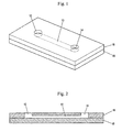
- FIGS. 1 and 2 show a typical plastic micro chip used for a lab-on-a-chip.
- the plastic micro chip comprises an upper substrate 16, a lower substrate 18 and a sample filling space (channel) 10 having a predetermined height D or a fine structure, etc. between the upper and lower substrates.
- the channel should be precisely manufactured to have a height of several ⁇ m to several hundreds ⁇ m when manufacturing the plastic micro chip. Accordingly, it is required to very precisely and correctly bond the upper and lower substrates including the channel or fine structure so that the plastic micro chip can perfectly function. In addition, surface properties of main parts of the cartridge or the chip should be maintained as they are.
- the upper and lower substrates are generally bonded by a heat bonding, an ultrasonic bonding, an optical method or an adhesive using a primer.
- the heat bonding method is mainly used to bond the material such as a film.
- the optical method is a boding method using a specific molecular structure of the plastic surface and can be applied to some plastics only.
- the method using the adhesive is used even in daily life.
- the ultrasonic bonding method is actively used in industries.
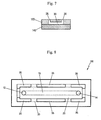
- FIGS. 3 and 4 show a bonding process according to an ultrasonic bonding method of the prior art.
- a protrusion is formed on a lower surface of an upper substrate 16 and a recess is formed in an upper surface of a lower substrate 18. Then, when an ultrasonic wave is applied with the upper and lower substrates 16, 18 being overlapped, the protrusion of the upper substrate 16 is melted and thus the upper substrate 16 is bonded to the lower substrate 18.
- the bonding surface is irregular and rough, an empty space can be formed and it is difficult to control the channel to have a predetermined height (D), so that an error can occur.
- the height of the channel should be also precisely controlled in order to precisely manufacture a volume of the channel.
- the channel is not completely sealed and an empty space can be thus formed, a sample in the channel can flow out to the exterior and an air bubble can occur in the sample inside of the channel.
- the present invention has been made to solve the above-mentioned problems occurring in the prior art.
- an organic solvent is introduced between an upper substrate and a lower substrate, and thus the substrates are easily and precisely bonded without an error when they are bonded.
- the object of the invention is to provide a method of bonding the upper and lower substrates in order to manufacture a plastic micro chip used for a lap-on-a-chip (LOC), etc.
- LOC lap-on-a-chip
- the invention relates to a method of bonding an upper substrate and a lower substrate in order to manufacture a plastic micro chip.
- the invention relates to a method of bonding an upper substrate and a lower substrate in order to manufacture a plastic micro chip comprising the upper substrate, the lower substrate and a sample filling space having a predetermined height for filling a sample between the upper and lower substrates, wherein the upper and lower substrates are bonded by introducing an organic solvent between the upper and lower substrates.
- the invention provides a method of manufacturing a plastic micro chip comprising an upper substrate, a lower substrate and a sample filling space having a predetermined height for filling a sample between the upper and lower substrates, comprising steps of:
- one or more holes for introducing the organic solvent communicating with the fine channel may be formed when the fine channel is formed in the step of (a).
- the plastic micro chip having a functional channel has a hydrophilic surface or a functional group such as amine group, carboxyl group or aldehyde capable of combining with a protein (for example, antigen, antibody or enzyme) or DNA.
- a protein for example, antigen, antibody or enzyme
- the plasma treatment is performed as described above, impurities are removed from the surface of the bonding region and a surface energy is increased, so that the solvent can flow well.
- the bonding strength can be increased. However, this treatment does not have influence on the surface of the chip.
- the channel When forming the fine channel, the channel can become opaque if a height of the channel is excessively high. Accordingly, it is preferred to form the fine channel so that the height thereof is not too high. For example, it is preferred to form the channel to have a height of about 100 ⁇ m or less.
- a plastic micro chip comprising an upper substrate, a lower substrate, a sample filling space having a predetermined height for filling a sample between the upper and lower substrates, and a fine channel defining a space for filling an organic solvent so as to bond the upper and lower substrates in a bonding region of a circumference of the sample filling space of the upper substrate.
- the plastic micro chip may comprise one or more holes for introducing the organic solvent communicating with the fine channel.
- the solvent in the fine channel can smoothly flow by pressurizing or decompressing the fine channel through the introducing hole.
- the upper and lower substrates are made of polyethylene derivatives such as polycarbonate, polystyrene, polypropylene and polyethyleneterephthalate, polymethylmethacrylate or an acryl based plastic materials.
- Any organic solvent capable of dissolving the material of the substrates may be used in the invention.
- ketone, aromatic hydrocarbon, halogenated hydrocarbon or cyanoacrylate compound or a mixture thereof is used.
- acetone, chloroform, methylene chloride, ethylcyanoacrylate or carbon tetrachloride or a mixture thereof is preferably used.
- FIG. 5 is a plan view of a plastic micro chip 100 for bonding according to an embodiment of the invention.
- FIG. 6 is a cross sectional view of the plastic micro chip in FIG. 5 taken along line A-A'.
- FIG. 7 is a cross sectional view of the plastic micro chip in FIG. 5 taken along line B-B'.
- the plastic micro chip 100 comprises an upper substrate 120, a lower substrate 140 and a sample filling space 10 having a predetermined height (D) for filling a sample between the upper substrate 120 and the lower substrate 140.
- a sample introducing hole 12 is formed at a side of the sample filling space 10 and a sample discharging hole 14 is formed at the other side.
- a fine channel space 30 having a height of 100 ⁇ m for filling a bonding organic solvent is formed in a bonding region 20 of a circumference of the sample filling space 10.
- organic solvent introducing holes 35 communicating with the fine channel are formed at each of the apexes so that the organic solvent can be introduced into the fine channel 30.
- the lower substrate 140 and the upper substrate 120 formed with the fine channel space 30 are overlapped each other, and the acetone is introduced into the organic solvent introducing holes 35 of the fine channel 30 in a small amount (few ⁇ l).
- the acetone flows along the fine channel 30 by the capillary phenomenon, and melts the upper substrate 120 and the lower substrate 140 in the bonding region 20 of the periphery of the fine channel 30, thereby bonding them.
- the acetone remaining in the fine channel 30 is rapidly evaporated into the air, and the bonding region 20 is firmly bonded while sealing the sample filling space 10 without a bonding tolerance.
- the plastic micro chip when the plastic micro chip is manufactured according to the method of the invention, it is possible to precisely and correctly bond the upper and lower substrates of the plastic micro chip. Particularly, it is possible to perfectly seal the sample filling space (channel) of the plastic micro chip and to correctly manufacture the channel having a desired height.
Abstract
Description
- The invention relates to a method of bonding a plastic micro chip, and more particularly to a method of bonding upper and lower substrates for manufacturing a plastic micro chip comprising the upper substrate, the lower substrate and a sample filling space having a predetermined height for filling a sample between the upper and lower substrates, wherein the upper and lower substrates are bonded by introducing an organic solvent between the upper and lower substrates. In addition, the invention relates to a method of manufacturing a micro chip using the boning method and a micro chip manufactured according to the method.
- Currently, researches and commercialization of a point of care (POC) and a lab-on-a-chip (LOC) (which means a laboratory on a chip and is a technology for diagnosing various diseases in a small chip at a time) are actively carried out in a bio-industry. Typically, products allowing for a rapid diagnosis and experiment as the POC or LOC are released as a product with a special surface treatment or reagent fixed in a plastic micro chip or cartridge. It can be said that the cartridge or chip is a core of the product.
- Generally, the plastic micro chip or cartridge used for the POC and LOC is made of polyethylene (PE) derivatives such as polycarbonate (PC), polystyrene (PS), polypropylene (PP) and polyethyleneterephthalate (PET), polymethylmethacrylate (PMAA) or an acryl based plastic, and is used as a disposable.
-
FIGS. 1 and 2 show a typical plastic micro chip used for a lab-on-a-chip. Generally, the plastic micro chip comprises anupper substrate 16, alower substrate 18 and a sample filling space (channel) 10 having a predetermined height D or a fine structure, etc. between the upper and lower substrates. - It is required that the channel should be precisely manufactured to have a height of several µm to several hundreds µm when manufacturing the plastic micro chip. Accordingly, it is required to very precisely and correctly bond the upper and lower substrates including the channel or fine structure so that the plastic micro chip can perfectly function. In addition, surface properties of main parts of the cartridge or the chip should be maintained as they are.
- When manufacturing the plastic micro chip, the upper and lower substrates are generally bonded by a heat bonding, an ultrasonic bonding, an optical method or an adhesive using a primer.
- The heat bonding method is mainly used to bond the material such as a film. The optical method is a boding method using a specific molecular structure of the plastic surface and can be applied to some plastics only. The method using the adhesive is used even in daily life. The ultrasonic bonding method is actively used in industries.
- However, there are some disadvantages when bonding the plastic micro chip using the above methods. In other words, there is a limitation in correctly and precisely bonding the chip having the fine channel or structure without an error, and it is difficult to bond the chip without influencing on properties of an inner surface thereof.
-
FIGS. 3 and 4 show a bonding process according to an ultrasonic bonding method of the prior art. - As shown in
FIG. 3 , a protrusion is formed on a lower surface of anupper substrate 16 and a recess is formed in an upper surface of alower substrate 18. Then, when an ultrasonic wave is applied with the upper andlower substrates upper substrate 16 is melted and thus theupper substrate 16 is bonded to thelower substrate 18. However, as shown inFIG. 4 , since the bonding surface is irregular and rough, an empty space can be formed and it is difficult to control the channel to have a predetermined height (D), so that an error can occur. - Generally, in a plastic micro chip, the height of the channel should be also precisely controlled in order to precisely manufacture a volume of the channel. However, it is difficult to precisely control the height of the channel with the prior bonding methods.
- In addition, since the channel is not completely sealed and an empty space can be thus formed, a sample in the channel can flow out to the exterior and an air bubble can occur in the sample inside of the channel.
- Accordingly, the present invention has been made to solve the above-mentioned problems occurring in the prior art. In the present invention, an organic solvent is introduced between an upper substrate and a lower substrate, and thus the substrates are easily and precisely bonded without an error when they are bonded.
- The object of the invention is to provide a method of bonding the upper and lower substrates in order to manufacture a plastic micro chip used for a lap-on-a-chip (LOC), etc.
- It is another object to provide a method of manufacturing a plastic micro chip using the bonding method.
- It is yet another object to provide a plastic micro chip manufactured by the bonding method.
- The invention relates to a method of bonding an upper substrate and a lower substrate in order to manufacture a plastic micro chip.
- More specifically, the invention relates to a method of bonding an upper substrate and a lower substrate in order to manufacture a plastic micro chip comprising the upper substrate, the lower substrate and a sample filling space having a predetermined height for filling a sample between the upper and lower substrates, wherein the upper and lower substrates are bonded by introducing an organic solvent between the upper and lower substrates.
- In addition, the invention provides a method of manufacturing a plastic micro chip comprising an upper substrate, a lower substrate and a sample filling space having a predetermined height for filling a sample between the upper and lower substrates, comprising steps of:
- (a) forming a fine channel space for filling a bonding organic solvent in a bonding region of a circumference of the sample filling space; and
- (b) overlapping the upper and lower substrates each other, and then introducing the organic solvent into the fine channel to bond the upper and lower substrates.
- Preferably, one or more holes for introducing the organic solvent communicating with the fine channel may be formed when the fine channel is formed in the step of (a).
- After forming the fine channel, it may preferably to perform a corona or plasma treatment for the bonding area so that the organic solvent subsequently introduced smoothly flows and a bonding strength is increased. The plastic micro chip having a functional channel has a hydrophilic surface or a functional group such as amine group, carboxyl group or aldehyde capable of combining with a protein (for example, antigen, antibody or enzyme) or DNA. When the plasma treatment is performed as described above, impurities are removed from the surface of the bonding region and a surface energy is increased, so that the solvent can flow well. In addition, the bonding strength can be increased. However, this treatment does not have influence on the surface of the chip.
- When forming the fine channel, the channel can become opaque if a height of the channel is excessively high. Accordingly, it is preferred to form the fine channel so that the height thereof is not too high. For example, it is preferred to form the channel to have a height of about 100 µm or less.
- In addition, according to the invention, there is provided a plastic micro chip comprising an upper substrate, a lower substrate, a sample filling space having a predetermined height for filling a sample between the upper and lower substrates, and a fine channel defining a space for filling an organic solvent so as to bond the upper and lower substrates in a bonding region of a circumference of the sample filling space of the upper substrate.
- Preferably, the plastic micro chip may comprise one or more holes for introducing the organic solvent communicating with the fine channel. The solvent in the fine channel can smoothly flow by pressurizing or decompressing the fine channel through the introducing hole.
- According to the invention, the upper and lower substrates are made of polyethylene derivatives such as polycarbonate, polystyrene, polypropylene and polyethyleneterephthalate, polymethylmethacrylate or an acryl based plastic materials.
- Any organic solvent capable of dissolving the material of the substrates may be used in the invention. For example, ketone, aromatic hydrocarbon, halogenated hydrocarbon or cyanoacrylate compound or a mixture thereof is used. Especially, acetone, chloroform, methylene chloride, ethylcyanoacrylate or carbon tetrachloride or a mixture thereof is preferably used.
- A more complete appreciation of the invention, and many of the attendant advantages thereof, will be readily apparent as the same becomes better understood by reference to the following detailed description when considered in conjunction with the accompanying drawings in which like reference symbols indicate the same or similar components, wherein:
-
FIGS. 1 and 2 are a perspective view and a cross sectional view of a conventional plastic micro chip; -
FIGS. 3 and 4 show a method of bonding an upper substrate and a lower substrate of a plastic micro chip according to the prior art; -
FIG. 5 is a plan view of a plastic micro chip according to a first embodiment of the invention; -
FIG. 6 is a cross sectional view of the plastic micro chip inFIG. 5 taken along line A-A'; -
FIG. 7 is a cross sectional view of the plastic micro chip inFIG. 5 taken along line B-B'; -
FIG. 8 is a plan view of a plastic micro chip according to a second embodiment of the invention; and -
FIG. 9 is a cross sectional view of a plastic micro chip according to a third embodiment of the invention. - Hereinafter, preferred embodiments of the present invention will be described with reference to the accompanying drawings. In the following description of the present invention, a detailed description of known functions and configurations incorporated herein will be omitted when it may make the subject matter of the present invention rather unclear.
-
FIG. 5 is a plan view of a plasticmicro chip 100 for bonding according to an embodiment of the invention.FIG. 6 is a cross sectional view of the plastic micro chip inFIG. 5 taken along line A-A'.FIG. 7 is a cross sectional view of the plastic micro chip inFIG. 5 taken along line B-B'. - The plastic
micro chip 100 comprises anupper substrate 120, alower substrate 140 and asample filling space 10 having a predetermined height (D) for filling a sample between theupper substrate 120 and thelower substrate 140. Asample introducing hole 12 is formed at a side of thesample filling space 10 and asample discharging hole 14 is formed at the other side. - A
fine channel space 30 having a height of 100 µm for filling a bonding organic solvent is formed in abonding region 20 of a circumference of thesample filling space 10. In addition, organicsolvent introducing holes 35 communicating with the fine channel are formed at each of the apexes so that the organic solvent can be introduced into thefine channel 30. - Surfaces of the
upper substrate 120 and thelower substrate 140 are plasma-treated so that an organic solvent (for example, acetone) subsequently introduced can flow well. - After that, in order to bond the
upper substrate 120 and thelower substrate 140, thelower substrate 140 and theupper substrate 120 formed with thefine channel space 30 are overlapped each other, and the acetone is introduced into the organicsolvent introducing holes 35 of thefine channel 30 in a small amount (few µl). The acetone flows along thefine channel 30 by the capillary phenomenon, and melts theupper substrate 120 and thelower substrate 140 in thebonding region 20 of the periphery of thefine channel 30, thereby bonding them. - The acetone remaining in the
fine channel 30 is rapidly evaporated into the air, and thebonding region 20 is firmly bonded while sealing thesample filling space 10 without a bonding tolerance. -
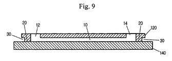
FIG. 8 shows a plastic micro chip having an enlarged organic solvent introducingholes 35 for easily introducing the organic solvent into thefine channel space 30. -
FIG. 9 is a cross sectional view of a plastic micro chip according to a third embodiment of the invention. The plastic micro chip according to the third embodiment of the invention includesrecesses 30 formed in each of side lower ends of theupper substrate 120. Theupper substrate 120 and thelower substrate 140 of thebonding region 20 can be bonded each other by introducing the organic solvent into the recesses. - As described above, when the plastic micro chip is manufactured according to the method of the invention, it is possible to precisely and correctly bond the upper and lower substrates of the plastic micro chip. Particularly, it is possible to perfectly seal the sample filling space (channel) of the plastic micro chip and to correctly manufacture the channel having a desired height.
- While the invention has been shown and described with reference to certain preferred embodiments thereof, it will be understood by those skilled in the art that various changes in form and details may be made therein without departing from the spirit and scope of the invention as defined by the appended claims.
- Certain specific embodiments of the invention are set forth below:
- A. A method of bonding an upper substrate and a lower substrate in order to manufacture a plastic micro chip comprising the upper substrate, the lower substrate and a sample filling space having a predetermined height for filling a sample between the upper and lower substrates, wherein the upper and lower substrates are bonded by introducing and organic solvent between the upper and lower substrates.
- B. A method of manufacturing a plastic micro chip comprising an upper substrate, a lower substrate and a sample filling space having a predetermined height for filling a sample between the upper and lower substrates, comprising steps of:
- (a) forming a fine channel space for filling a bonding organic solvent in a bonding region of a circumstance of the sample filling space; and
- (b) overlapping the upper and lower substrates each other, and then introducing the organic solvent into the fine channel to bond the upper and lower substrates.
- C. The method according to B, further comprising a step of forming one or more holes for introducing the organic solvent communicating with the fine channel when the fine channel is formed in the step of (a).
- D. The method according to B, further comprising a step of performing a corona or plasma treatment for the bonding area so that the organic solvent subsequently introduced smoothly flows and a bonding strength is increased, after forming the fine channel.
- E. The method according to B, wherein the fine channel has a height of 100 µm or less.
- F. The method according to B, wherein the step of (b) further comprises a sub-step of pressurizing or decompressing the fine channel after introducing the organic solvent into the fine channel.
- G. The method according to A or B, wherein the organic solvent is at least one selected from a group consisting of ketone, aromatic hydrocarbon, cyanoacrylate compound and halogenated hydrocarbon.
- H. The method according to G, wherein the organic solvent is at least on selected from a group consisting of acetone, chloroform, methylene chloride, ethylcyanoacrylate and carbon tetrachloride.
- I. The method according to A or B, wherein the upper and lower substrates are made of polycarbonate, polystyrene, polyproplene, polyethylene derivatives or polymethylmethacrylate.
- K. A plastic micro chip comprising:
- an upper substrate, a lower substrate, a sample filling space having a predetermined height for filling a sample between the upper and lower substrates, and a fine channel defining a space for filling an organic solvent so as to bond the upper and lower substrates in a bonding region of a circumference of the sample filling space of the upper substrate.
- L. The plastic micro chip according to K, further comprising one or more holes for introducing the organic solvent communicating with the fine channel.
- M. The plastic micro chip according to K, wherein the organic solvent is at least one selected from a group consisting of ketone, aromatic hydrocarbon, cyanocrylate compound and halogenated hydrocarbon.
- N. The plastic micro chip according to M, wherein the organic solvent is at least one selected from a group consisting of acetone, chloroform, methylene chloride, ethylcyanoacrylate and carbon tetrachloride.
- O. The Plastic micro chip according to K, wherein the fine channel has a height of 100 µm or less.
- P. The plastic micro chip according to K, wherein the bonding region is transparent.
- Q. The plastic micro chip according to K, wherein the upper and lower substrates are made of polycarbonate, polystyrene, polypropylene, polyethylene derivatives, polymethylmethacrylate or acryl-based plastic material.
| 100 : | plastic micro chip | 120 : | upper substrate |
| 140 : | lower substrate | 10 : | sample filling space |
| 12 : | sample introducing hole | 14 : | sample discharging hole |
| 20 : | bonding region | 30 : | fine channel |
| 35 : | organic solvent introducing hole | D : | height of sample filling space |
Claims (4)
- A method of manufacturing a plastic micro chip comprising an upper substrate, a lower substrate and a sample filling space having a predetermined height for filling a sample between the upper and lower substrates, comprising the steps of:(a) forming recesses in each of side lower ends of the upper substrate(b) overlapping the upper substrate and the lower substrate each other; and(c) introducing an organic solvent into the recesses to bond the upper and lower substrates, wherein the recesses are open channels,wherein the upper substrate and the lower substrate are bonded by the organic solvent introduced through the recesses being introduced into between the upper substrate and the lower substrate,
wherein a bonding region is circumference of the sample filling space and periphery of the recesses. - The method according to claim 1, wherein the organic solvent is at least one selected from a group consisting of ketone, aromatic hydrocarbon, cyanoacrylate compound and halogenated hydrocarbon.
- The method according to claim 1, wherein the organic solvent is at least one selected from a group consisting of acetone, chloroform, methylene chloride, ethylcyanoacrylate and carbon tetrachloride.
- A plastic micro chip comprising :an upper substrate;a lower substrate;a sample filling space having a predetermined height for filling a sample between the upper and lower substrates; andrecesses for introducing organic solvent into the recesses in each of side lower ends of the upper substrate,wherein the upper substrate and the lower substrate are bonded by the organic solvent introduced through the recesses being introduced into between the upper substrate and the lower substrate,wherein a bonding region is circumference of the sample filling space and periphery of the recesses.
Applications Claiming Priority (2)
| Application Number | Priority Date | Filing Date | Title |
|---|---|---|---|
| KR20030093443A KR100572207B1 (en) | 2003-12-18 | 2003-12-18 | Bonding method of plastic microchip |
| EP04808468A EP1697745A4 (en) | 2003-12-18 | 2004-12-17 | Method for bonding plastic micro chip |
Related Parent Applications (1)
| Application Number | Title | Priority Date | Filing Date |
|---|---|---|---|
| EP04808468.5 Division | 2004-12-17 |
Publications (3)
| Publication Number | Publication Date |
|---|---|
| EP2251182A2 true EP2251182A2 (en) | 2010-11-17 |
| EP2251182A3 EP2251182A3 (en) | 2010-12-01 |
| EP2251182B1 EP2251182B1 (en) | 2012-01-25 |
Family
ID=36791151
Family Applications (2)
| Application Number | Title | Priority Date | Filing Date |
|---|---|---|---|
| EP20100006339 Active EP2251182B1 (en) | 2003-12-18 | 2004-12-17 | Method for bonding plastic micro chip |
| EP04808468A Withdrawn EP1697745A4 (en) | 2003-12-18 | 2004-12-17 | Method for bonding plastic micro chip |
Family Applications After (1)
| Application Number | Title | Priority Date | Filing Date |
|---|---|---|---|
| EP04808468A Withdrawn EP1697745A4 (en) | 2003-12-18 | 2004-12-17 | Method for bonding plastic micro chip |
Country Status (5)
| Country | Link |
|---|---|
| US (3) | US7842157B2 (en) |
| EP (2) | EP2251182B1 (en) |
| KR (1) | KR100572207B1 (en) |
| AT (1) | ATE542663T1 (en) |
| WO (1) | WO2005059549A1 (en) |
Cited By (1)
| Publication number | Priority date | Publication date | Assignee | Title |
|---|---|---|---|---|
| DE102012112306A1 (en) * | 2012-12-14 | 2014-06-18 | Thinxxs Microtechnology Ag | Method for connecting components of a microfluidic flow cell |
Families Citing this family (34)
| Publication number | Priority date | Publication date | Assignee | Title |
|---|---|---|---|---|
| KR20040105717A (en) | 2002-02-14 | 2004-12-16 | 이뮤니베스트 코포레이션 | Methods and algorithms for cell enumeration in a low-cost cytometer |
| US7764821B2 (en) | 2002-02-14 | 2010-07-27 | Veridex, Llc | Methods and algorithms for cell enumeration in a low-cost cytometer |
| KR100572207B1 (en) * | 2003-12-18 | 2006-04-19 | 주식회사 디지탈바이오테크놀러지 | Bonding method of plastic microchip |
| CA2563002C (en) * | 2004-04-07 | 2011-07-12 | Wardlaw Partners Lp | Disposable chamber for analyzing biologic fluids |
| US8189899B2 (en) | 2004-07-30 | 2012-05-29 | Veridex, Llc | Methods and algorithms for cell enumeration in a low-cost cytometer |
| US7731901B2 (en) | 2005-10-19 | 2010-06-08 | Abbott Laboratories | Apparatus and method for performing counts within a biologic fluid sample |
| GB0524854D0 (en) * | 2005-12-06 | 2006-01-11 | Epigem Ltd | Fine line bonding and/or sealing system and method |
| KR100905954B1 (en) * | 2007-07-23 | 2009-07-06 | 주식회사 디지탈바이오테크놀러지 | Module for detecting analytes in fluids and chip having the same |
| EP2031743B1 (en) * | 2007-08-30 | 2018-06-20 | Johnson Electric S.A. | DC-motor with commutator |
| KR20090074397A (en) * | 2008-01-02 | 2009-07-07 | 삼성전자주식회사 | Microfluidic device and fabricating method of the same |
| KR20100019615A (en) * | 2008-08-11 | 2010-02-19 | 삼성전자주식회사 | Joint body and manufacturing method of the same |
| US20110182775A1 (en) * | 2008-10-05 | 2011-07-28 | Arkray, Inc. | Analytical instrument and method for manufacturing same |
| KR100961850B1 (en) | 2008-10-30 | 2010-06-09 | 주식회사 올메디쿠스 | Microfluidic chip using hydrophillic film |
| CN101770128B (en) * | 2009-01-07 | 2016-05-11 | 德昌电机(深圳)有限公司 | Electrophoretic display apparatus |
| US9579651B2 (en) * | 2009-12-18 | 2017-02-28 | Abbott Point Of Care, Inc. | Biologic fluid analysis cartridge |
| CN103282123B (en) | 2010-12-30 | 2015-05-06 | 艾博特健康公司 | Biologic fluid analysis cartridge with sample handling portion and analysis chamber portion |
| KR101242540B1 (en) * | 2011-08-19 | 2013-03-19 | (주)로고스바이오시스템스 | Microchip |
| EP2748618A1 (en) | 2011-08-24 | 2014-07-02 | Abbott Point of Care Inc. | Biologic fluid sample analysis cartridge |
| WO2014139751A1 (en) * | 2013-03-14 | 2014-09-18 | Sony Corporation | Microfluidic device |
| GB201311680D0 (en) * | 2013-06-28 | 2013-08-14 | Ibm | Fabrication of a microfluidic chip package or assembly with separable chips |
| US20160184820A1 (en) * | 2013-08-14 | 2016-06-30 | Sony Dadc Austria Ag | Microfluidic device |
| JP5933518B2 (en) * | 2013-12-26 | 2016-06-08 | 富士フイルム株式会社 | Bonding method and manufacturing method of microchannel device |
| US9787345B2 (en) * | 2014-03-31 | 2017-10-10 | Apple Inc. | Laser welding of transparent and opaque materials |
| KR101585329B1 (en) * | 2014-06-03 | 2016-01-15 | 주식회사 나노엔텍 | plastic microchip |
| US10200516B2 (en) | 2014-08-28 | 2019-02-05 | Apple Inc. | Interlocking ceramic and optical members |
| US10525464B2 (en) | 2014-09-02 | 2020-01-07 | Bio-Rad Laboratories, Inc. | Microscale fluidic devices and components having a fluid retention groove |
| JP6010641B2 (en) * | 2015-01-28 | 2016-10-19 | 富士重工業株式会社 | Resin member and joining method of resin member |
| CN104960195A (en) * | 2015-06-19 | 2015-10-07 | 大连理工大学 | Joint structure used for flow casting control and weld stopping control of POCT chip product ultrasonic welding |
| CN105109034A (en) * | 2015-09-25 | 2015-12-02 | 大连理工大学 | Joint structure used for precise ultrasonic welding of POCT chip products |
| USD816861S1 (en) * | 2016-09-07 | 2018-05-01 | EMULATE, Inc. | Transparent microfluidic chip without pressure features for use with a fluid perfusion module |
| USD842493S1 (en) * | 2016-09-07 | 2019-03-05 | EMULATE, Inc. | Microfluidic chip without pressure features for use with a fluid perfusion module |
| BG67480B1 (en) | 2019-10-30 | 2022-12-15 | "Милкотроник" Оод | Device for differential counting of microparticles in biological liquids |
| CN111751272B (en) * | 2020-07-03 | 2021-09-07 | 北京理工大学 | Ultrasonic detection and tensile calibration test method for bonding strength grade |
| CN113058671A (en) * | 2021-04-20 | 2021-07-02 | 中国人民解放军军事科学院军事医学研究院 | Manufacturing method of energy guiding rib for bonding of micro-fluidic chip |
Family Cites Families (48)
| Publication number | Priority date | Publication date | Assignee | Title |
|---|---|---|---|---|
| US4181549A (en) * | 1977-03-10 | 1980-01-01 | American Hospital Supply Corporation | Solvent-bonded joint and method of making the same |
| US4171866A (en) | 1978-04-20 | 1979-10-23 | Tolles Walter E | Disposable volumetric slide |
| JPS582709U (en) * | 1981-06-27 | 1983-01-08 | 富士通株式会社 | Pressurized box body with adhesive part |
| JPS5863382A (en) * | 1981-10-13 | 1983-04-15 | Terumo Corp | Multi-layer culture test tool for microorganism |
| US4357369A (en) * | 1981-11-10 | 1982-11-02 | Rca Corporation | Method of plasma etching a substrate |
| DK429682A (en) | 1982-09-28 | 1984-03-29 | Inflow Aps | INTEGRATED MICRO-ROOM SYSTEMS FOR CONTINUOUS FLOW ANALYSIS |
| US4651382A (en) * | 1984-05-31 | 1987-03-24 | Krolick Robert S | Solvent-bondable plastic parts with capillary-action blocking moat to confine solvent flow |
| US5259894A (en) * | 1990-01-26 | 1993-11-09 | Sampson Richard K | Method for solvent bonding non-porous materials to automatically create variable bond characteristics |
| US6176962B1 (en) | 1990-02-28 | 2001-01-23 | Aclara Biosciences, Inc. | Methods for fabricating enclosed microchannel structures |
| JP3092674B2 (en) * | 1991-08-08 | 2000-09-25 | 株式会社ニッショー | How to connect a medical tube |
| US5259835A (en) * | 1991-08-29 | 1993-11-09 | Tri-Point Medical L.P. | Wound closure means and method using flowable adhesive |
| US5259874A (en) | 1991-10-23 | 1993-11-09 | Hewlett-Packard Company | Solid ink compositions suitable for use in color transparencies |
| US5349436A (en) | 1992-12-02 | 1994-09-20 | Harry Fisch | Biological assembly |
| DE4414915C2 (en) * | 1994-04-28 | 2001-01-18 | Karlsruhe Forschzent | Process for gluing microstructures |
| CA2161040A1 (en) * | 1994-10-21 | 1996-04-22 | Delbert D. Derees | Vehicle assembly method |
| GB9422783D0 (en) * | 1994-11-11 | 1995-01-04 | Rotalac Plastics | Bonding |
| US6482742B1 (en) * | 2000-07-18 | 2002-11-19 | Stephen Y. Chou | Fluid pressure imprint lithography |
| US20010055812A1 (en) * | 1995-12-05 | 2001-12-27 | Alec Mian | Devices and method for using centripetal acceleration to drive fluid movement in a microfluidics system with on-board informatics |
| DE19632275C2 (en) | 1996-08-09 | 2001-02-22 | Drei Bond Gmbh Chemische Verbi | Sealing and adhesive process for component connections |
| US6052224A (en) | 1997-03-21 | 2000-04-18 | Northern Edge Associates | Microscope slide system and method of use |
| US6425972B1 (en) * | 1997-06-18 | 2002-07-30 | Calipher Technologies Corp. | Methods of manufacturing microfabricated substrates |
| US5882465A (en) | 1997-06-18 | 1999-03-16 | Caliper Technologies Corp. | Method of manufacturing microfluidic devices |
| US6375871B1 (en) * | 1998-06-18 | 2002-04-23 | 3M Innovative Properties Company | Methods of manufacturing microfluidic articles |
| CA2301557A1 (en) * | 1997-09-19 | 1999-04-01 | Aclara Biosciences, Inc. | Apparatus and method for transferring liquids |
| WO1999025783A1 (en) * | 1997-11-14 | 1999-05-27 | INSTITUT FüR MIKROTECHNIK MAINZ GMBH | Process for joining microstructured plastic parts and component produced by this process |
| US6756019B1 (en) | 1998-02-24 | 2004-06-29 | Caliper Technologies Corp. | Microfluidic devices and systems incorporating cover layers |
| US6251343B1 (en) | 1998-02-24 | 2001-06-26 | Caliper Technologies Corp. | Microfluidic devices and systems incorporating cover layers |
| US6329224B1 (en) * | 1998-04-28 | 2001-12-11 | Tessera, Inc. | Encapsulation of microelectronic assemblies |
| US6123798A (en) | 1998-05-06 | 2000-09-26 | Caliper Technologies Corp. | Methods of fabricating polymeric structures incorporating microscale fluidic elements |
| DE19922075A1 (en) * | 1999-05-14 | 2000-11-16 | Inst Mikrotechnik Mainz Gmbh | Bonding two microstructured plastics workpieces together, comprises introducing a plastics-dissolving organic solvent into a groove between the workpieces |
| JP3623479B2 (en) | 1999-06-22 | 2005-02-23 | テカン トレーディング アーゲー | Apparatus and method for performing miniaturized in vitro amplification assays |
| US7163121B1 (en) | 1999-07-14 | 2007-01-16 | Swales & Associates, Inc. | High temperature isostatic pressure bonding of hollow beryllium pressure vessels using a bonding flange |
| WO2001026812A1 (en) | 1999-10-14 | 2001-04-19 | Ce Resources Pte Ltd | Microfluidic structures and methods of fabrication |
| JP3528732B2 (en) * | 2000-01-11 | 2004-05-24 | 株式会社島津製作所 | Measurement cell |
| CA2406707A1 (en) | 2000-04-06 | 2001-10-18 | Robert Nagle | Microfluidic devices and systems incorporating cover layers |
| US6561208B1 (en) | 2000-04-14 | 2003-05-13 | Nanostream, Inc. | Fluidic impedances in microfluidic system |
| US20020151078A1 (en) * | 2000-05-15 | 2002-10-17 | Kellogg Gregory J. | Microfluidics devices and methods for high throughput screening |
| US6673440B2 (en) * | 2000-11-06 | 2004-01-06 | Sterling Medivations, Inc. | Subcutaneous injection set tubing with solvent bonding |
| AU2002248149A1 (en) | 2000-11-16 | 2002-08-12 | Fluidigm Corporation | Microfluidic devices for introducing and dispensing fluids from microfluidic systems |
| EP1296133A1 (en) | 2001-09-21 | 2003-03-26 | Jean Brunner | Miniature device for transport and analysis of a liquid sample and fabrication method therefor |
| KR20030032812A (en) * | 2001-10-17 | 2003-04-26 | 장준근 | Microchip for measuring blood coagulation and apparatus for measuring blood coagulation using the same |
| US7514045B2 (en) | 2002-01-18 | 2009-04-07 | Avery Dennison Corporation | Covered microchamber structures |
| US20040241381A1 (en) * | 2002-01-31 | 2004-12-02 | Chen Yihfar | Microfluidic structures with circumferential grooves for bonding adhesives and related optical analysis discs |
| US6827811B2 (en) * | 2002-02-07 | 2004-12-07 | Lynntech, Inc. | Method for vacuum pressing electrochemical cell components |
| US7226564B2 (en) | 2002-07-26 | 2007-06-05 | Enplas Corporation | Plate assembly |
| US7125711B2 (en) * | 2002-12-19 | 2006-10-24 | Bayer Healthcare Llc | Method and apparatus for splitting of specimens into multiple channels of a microfluidic device |
| KR100572207B1 (en) | 2003-12-18 | 2006-04-19 | 주식회사 디지탈바이오테크놀러지 | Bonding method of plastic microchip |
| KR101058673B1 (en) * | 2004-02-10 | 2011-08-22 | 삼성전자주식회사 | Text image transmission method of mobile terminal |
-
2003
- 2003-12-18 KR KR20030093443A patent/KR100572207B1/en active IP Right Review Request
-
2004
- 2004-12-17 EP EP20100006339 patent/EP2251182B1/en active Active
- 2004-12-17 EP EP04808468A patent/EP1697745A4/en not_active Withdrawn
- 2004-12-17 WO PCT/KR2004/003337 patent/WO2005059549A1/en not_active Application Discontinuation
- 2004-12-17 AT AT10006339T patent/ATE542663T1/en active
- 2004-12-17 US US10/583,149 patent/US7842157B2/en active Active
-
2010
- 2010-10-29 US US12/916,098 patent/US8900531B2/en active Active
-
2014
- 2014-11-26 US US14/555,299 patent/US20150114556A1/en not_active Abandoned
Non-Patent Citations (1)
| Title |
|---|
| None |
Cited By (1)
| Publication number | Priority date | Publication date | Assignee | Title |
|---|---|---|---|---|
| DE102012112306A1 (en) * | 2012-12-14 | 2014-06-18 | Thinxxs Microtechnology Ag | Method for connecting components of a microfluidic flow cell |
Also Published As
| Publication number | Publication date |
|---|---|
| EP1697745A4 (en) | 2009-01-21 |
| ATE542663T1 (en) | 2012-02-15 |
| EP2251182A3 (en) | 2010-12-01 |
| US20150114556A1 (en) | 2015-04-30 |
| US7842157B2 (en) | 2010-11-30 |
| KR100572207B1 (en) | 2006-04-19 |
| WO2005059549A1 (en) | 2005-06-30 |
| US20070141805A1 (en) | 2007-06-21 |
| US20110044862A1 (en) | 2011-02-24 |
| KR20050061886A (en) | 2005-06-23 |
| EP2251182B1 (en) | 2012-01-25 |
| US8900531B2 (en) | 2014-12-02 |
| EP1697745A1 (en) | 2006-09-06 |
Similar Documents
| Publication | Publication Date | Title |
|---|---|---|
| EP2251182A2 (en) | Method for bonding plastic micro chip | |
| US8377393B2 (en) | Microchip | |
| EP1115573B1 (en) | Methods of fabricating polymeric structures incorporating microscale fluidic elements | |
| US9283561B2 (en) | Liquid channel device and production method therefor | |
| KR100998535B1 (en) | Microfluidic circuit element comprising microfluidic channel with nano interstices and fabrication thereof | |
| JP4998462B2 (en) | Manufacturing method of resin composite molded body | |
| US10099218B2 (en) | Method for manufacturing and/or packaging a chip | |
| WO2007094254A1 (en) | Microchannel chip and method for manufacturing such chip | |
| US20120230887A1 (en) | Devices and methods for interfacing microfluidic devices with macrofluidic devices | |
| JPWO2008087800A1 (en) | Microchip manufacturing method and microchip | |
| JP2005257283A (en) | Microchip | |
| US9579653B2 (en) | Liquid channel device and production method therefor | |
| JP2010043928A (en) | Manufacturing method of biochip, and the biochip | |
| JP2008175795A (en) | Microchip made of plastic, and manufacturing method thereof, biochip or microanalysis chip using the same | |
| EP3231507A1 (en) | Fluid handling device and method for manufacturing fluid handling device | |
| JP2009047438A (en) | Micro flow-path chip | |
| US20130280144A1 (en) | Microchip | |
| JP2007240461A (en) | Plastic microchip, joining method therefor, and biochip or micro analytical chip using the same | |
| KR20110075448A (en) | A method for manufacturing a microfluidic device and a microfluidic divice manufactured using the same method | |
| JP2008157644A (en) | Plastic microchip, and biochip or micro analysis chip using the same | |
| EP2241895A1 (en) | Microchip and method for manufacturing the same | |
| JP2008076208A (en) | Plastic microchip, biochip using it or microanalyzing chip | |
| WO2009101850A1 (en) | Method for manufacturing microchip and microchip | |
| WO2010016371A1 (en) | Microchip, microchip manufacturing method and microchip manufacturing device | |
| JP2009192421A (en) | Method of manufacturing microchip and microchip |
Legal Events
| Date | Code | Title | Description |
|---|---|---|---|
| PUAI | Public reference made under article 153(3) epc to a published international application that has entered the european phase |
Free format text: ORIGINAL CODE: 0009012 |
|
| PUAL | Search report despatched |
Free format text: ORIGINAL CODE: 0009013 |
|
| 17P | Request for examination filed |
Effective date: 20100618 |
|
| AC | Divisional application: reference to earlier application |
Ref document number: 1697745 Country of ref document: EP Kind code of ref document: P |
|
| AK | Designated contracting states |
Kind code of ref document: A2 Designated state(s): AT BE BG CH CY CZ DE DK EE ES FI FR GB GR HU IE IS IT LI LT LU MC NL PL PT RO SE SI SK TR |
|
| AK | Designated contracting states |
Kind code of ref document: A3 Designated state(s): AT BE BG CH CY CZ DE DK EE ES FI FR GB GR HU IE IS IT LI LT LU MC NL PL PT RO SE SI SK TR |
|
| RIN1 | Information on inventor provided before grant (corrected) |
Inventor name: CHANG, JUN KEUN Inventor name: JO, HAN SANG Inventor name: PARK, JUN HA Inventor name: HUR, DAE SUNG Inventor name: CHUNG, CHANIL |
|
| RIN1 | Information on inventor provided before grant (corrected) |
Inventor name: HUR, DAE SUNG Inventor name: PARK, JUN HA Inventor name: CHANG, JUN KEUN Inventor name: JO, HAN SANG Inventor name: CHUNG, CHANIL |
|
| GRAP | Despatch of communication of intention to grant a patent |
Free format text: ORIGINAL CODE: EPIDOSNIGR1 |
|
| RIC1 | Information provided on ipc code assigned before grant |
Ipc: B29C 65/48 20060101AFI20110729BHEP Ipc: B01L 3/00 20060101ALI20110729BHEP |
|
| GRAS | Grant fee paid |
Free format text: ORIGINAL CODE: EPIDOSNIGR3 |
|
| GRAA | (expected) grant |
Free format text: ORIGINAL CODE: 0009210 |
|
| AC | Divisional application: reference to earlier application |
Ref document number: 1697745 Country of ref document: EP Kind code of ref document: P |
|
| AK | Designated contracting states |
Kind code of ref document: B1 Designated state(s): AT BE BG CH CY CZ DE DK EE ES FI FR GB GR HU IE IS IT LI LT LU MC NL PL PT RO SE SI SK TR |
|
| REG | Reference to a national code |
Ref country code: GB Ref legal event code: FG4D |
|
| REG | Reference to a national code |
Ref country code: CH Ref legal event code: EP |
|
| REG | Reference to a national code |
Ref country code: AT Ref legal event code: REF Ref document number: 542663 Country of ref document: AT Kind code of ref document: T Effective date: 20120215 |
|
| REG | Reference to a national code |
Ref country code: IE Ref legal event code: FG4D |
|
| REG | Reference to a national code |
Ref country code: DE Ref legal event code: R096 Ref document number: 602004036337 Country of ref document: DE Effective date: 20120322 |
|
| RAP2 | Party data changed (patent owner data changed or rights of a patent transferred) |
Owner name: NANOENTEK, INC. |
|
| REG | Reference to a national code |
Ref country code: NL Ref legal event code: VDEP Effective date: 20120125 |
|
| LTIE | Lt: invalidation of european patent or patent extension |
Effective date: 20120125 |
|
| REG | Reference to a national code |
Ref country code: GB Ref legal event code: 732E Free format text: REGISTERED BETWEEN 20120621 AND 20120627 |
|
| PG25 | Lapsed in a contracting state [announced via postgrant information from national office to epo] |
Ref country code: BE Free format text: LAPSE BECAUSE OF FAILURE TO SUBMIT A TRANSLATION OF THE DESCRIPTION OR TO PAY THE FEE WITHIN THE PRESCRIBED TIME-LIMIT Effective date: 20120125 Ref country code: BG Free format text: LAPSE BECAUSE OF FAILURE TO SUBMIT A TRANSLATION OF THE DESCRIPTION OR TO PAY THE FEE WITHIN THE PRESCRIBED TIME-LIMIT Effective date: 20120425 Ref country code: IS Free format text: LAPSE BECAUSE OF FAILURE TO SUBMIT A TRANSLATION OF THE DESCRIPTION OR TO PAY THE FEE WITHIN THE PRESCRIBED TIME-LIMIT Effective date: 20120525 Ref country code: LT Free format text: LAPSE BECAUSE OF FAILURE TO SUBMIT A TRANSLATION OF THE DESCRIPTION OR TO PAY THE FEE WITHIN THE PRESCRIBED TIME-LIMIT Effective date: 20120125 Ref country code: NL Free format text: LAPSE BECAUSE OF FAILURE TO SUBMIT A TRANSLATION OF THE DESCRIPTION OR TO PAY THE FEE WITHIN THE PRESCRIBED TIME-LIMIT Effective date: 20120125 |
|
| PG25 | Lapsed in a contracting state [announced via postgrant information from national office to epo] |
Ref country code: PT Free format text: LAPSE BECAUSE OF FAILURE TO SUBMIT A TRANSLATION OF THE DESCRIPTION OR TO PAY THE FEE WITHIN THE PRESCRIBED TIME-LIMIT Effective date: 20120525 Ref country code: FI Free format text: LAPSE BECAUSE OF FAILURE TO SUBMIT A TRANSLATION OF THE DESCRIPTION OR TO PAY THE FEE WITHIN THE PRESCRIBED TIME-LIMIT Effective date: 20120125 Ref country code: GR Free format text: LAPSE BECAUSE OF FAILURE TO SUBMIT A TRANSLATION OF THE DESCRIPTION OR TO PAY THE FEE WITHIN THE PRESCRIBED TIME-LIMIT Effective date: 20120426 Ref country code: PL Free format text: LAPSE BECAUSE OF FAILURE TO SUBMIT A TRANSLATION OF THE DESCRIPTION OR TO PAY THE FEE WITHIN THE PRESCRIBED TIME-LIMIT Effective date: 20120125 |
|
| REG | Reference to a national code |
Ref country code: AT Ref legal event code: MK05 Ref document number: 542663 Country of ref document: AT Kind code of ref document: T Effective date: 20120125 |
|
| PG25 | Lapsed in a contracting state [announced via postgrant information from national office to epo] |
Ref country code: CY Free format text: LAPSE BECAUSE OF FAILURE TO SUBMIT A TRANSLATION OF THE DESCRIPTION OR TO PAY THE FEE WITHIN THE PRESCRIBED TIME-LIMIT Effective date: 20120125 |
|
| PG25 | Lapsed in a contracting state [announced via postgrant information from national office to epo] |
Ref country code: SE Free format text: LAPSE BECAUSE OF FAILURE TO SUBMIT A TRANSLATION OF THE DESCRIPTION OR TO PAY THE FEE WITHIN THE PRESCRIBED TIME-LIMIT Effective date: 20120125 Ref country code: RO Free format text: LAPSE BECAUSE OF FAILURE TO SUBMIT A TRANSLATION OF THE DESCRIPTION OR TO PAY THE FEE WITHIN THE PRESCRIBED TIME-LIMIT Effective date: 20120125 Ref country code: CZ Free format text: LAPSE BECAUSE OF FAILURE TO SUBMIT A TRANSLATION OF THE DESCRIPTION OR TO PAY THE FEE WITHIN THE PRESCRIBED TIME-LIMIT Effective date: 20120125 Ref country code: SI Free format text: LAPSE BECAUSE OF FAILURE TO SUBMIT A TRANSLATION OF THE DESCRIPTION OR TO PAY THE FEE WITHIN THE PRESCRIBED TIME-LIMIT Effective date: 20120125 Ref country code: EE Free format text: LAPSE BECAUSE OF FAILURE TO SUBMIT A TRANSLATION OF THE DESCRIPTION OR TO PAY THE FEE WITHIN THE PRESCRIBED TIME-LIMIT Effective date: 20120125 Ref country code: DK Free format text: LAPSE BECAUSE OF FAILURE TO SUBMIT A TRANSLATION OF THE DESCRIPTION OR TO PAY THE FEE WITHIN THE PRESCRIBED TIME-LIMIT Effective date: 20120125 |
|
| PG25 | Lapsed in a contracting state [announced via postgrant information from national office to epo] |
Ref country code: IT Free format text: LAPSE BECAUSE OF FAILURE TO SUBMIT A TRANSLATION OF THE DESCRIPTION OR TO PAY THE FEE WITHIN THE PRESCRIBED TIME-LIMIT Effective date: 20120125 Ref country code: SK Free format text: LAPSE BECAUSE OF FAILURE TO SUBMIT A TRANSLATION OF THE DESCRIPTION OR TO PAY THE FEE WITHIN THE PRESCRIBED TIME-LIMIT Effective date: 20120125 |
|
| PLBE | No opposition filed within time limit |
Free format text: ORIGINAL CODE: 0009261 |
|
| STAA | Information on the status of an ep patent application or granted ep patent |
Free format text: STATUS: NO OPPOSITION FILED WITHIN TIME LIMIT |
|
| 26N | No opposition filed |
Effective date: 20121026 |
|
| PG25 | Lapsed in a contracting state [announced via postgrant information from national office to epo] |
Ref country code: AT Free format text: LAPSE BECAUSE OF FAILURE TO SUBMIT A TRANSLATION OF THE DESCRIPTION OR TO PAY THE FEE WITHIN THE PRESCRIBED TIME-LIMIT Effective date: 20120125 |
|
| REG | Reference to a national code |
Ref country code: DE Ref legal event code: R097 Ref document number: 602004036337 Country of ref document: DE Effective date: 20121026 |
|
| PG25 | Lapsed in a contracting state [announced via postgrant information from national office to epo] |
Ref country code: ES Free format text: LAPSE BECAUSE OF FAILURE TO SUBMIT A TRANSLATION OF THE DESCRIPTION OR TO PAY THE FEE WITHIN THE PRESCRIBED TIME-LIMIT Effective date: 20120506 |
|
| PG25 | Lapsed in a contracting state [announced via postgrant information from national office to epo] |
Ref country code: MC Free format text: LAPSE BECAUSE OF NON-PAYMENT OF DUE FEES Effective date: 20121231 |
|
| REG | Reference to a national code |
Ref country code: CH Ref legal event code: PL |
|
| REG | Reference to a national code |
Ref country code: IE Ref legal event code: MM4A |
|
| PG25 | Lapsed in a contracting state [announced via postgrant information from national office to epo] |
Ref country code: LI Free format text: LAPSE BECAUSE OF NON-PAYMENT OF DUE FEES Effective date: 20121231 Ref country code: CH Free format text: LAPSE BECAUSE OF NON-PAYMENT OF DUE FEES Effective date: 20121231 Ref country code: IE Free format text: LAPSE BECAUSE OF NON-PAYMENT OF DUE FEES Effective date: 20121217 |
|
| PG25 | Lapsed in a contracting state [announced via postgrant information from national office to epo] |
Ref country code: TR Free format text: LAPSE BECAUSE OF FAILURE TO SUBMIT A TRANSLATION OF THE DESCRIPTION OR TO PAY THE FEE WITHIN THE PRESCRIBED TIME-LIMIT Effective date: 20120125 |
|
| PG25 | Lapsed in a contracting state [announced via postgrant information from national office to epo] |
Ref country code: LU Free format text: LAPSE BECAUSE OF NON-PAYMENT OF DUE FEES Effective date: 20121217 |
|
| PG25 | Lapsed in a contracting state [announced via postgrant information from national office to epo] |
Ref country code: HU Free format text: LAPSE BECAUSE OF FAILURE TO SUBMIT A TRANSLATION OF THE DESCRIPTION OR TO PAY THE FEE WITHIN THE PRESCRIBED TIME-LIMIT Effective date: 20041217 |
|
| REG | Reference to a national code |
Ref country code: FR Ref legal event code: PLFP Year of fee payment: 12 |
|
| REG | Reference to a national code |
Ref country code: FR Ref legal event code: PLFP Year of fee payment: 13 |
|
| REG | Reference to a national code |
Ref country code: FR Ref legal event code: PLFP Year of fee payment: 14 |
|
| REG | Reference to a national code |
Ref country code: DE Ref legal event code: R082 Ref document number: 602004036337 Country of ref document: DE Representative=s name: SKM-IP SCHMID KRAUSS KUTTENKEULER MALESCHA SCH, DE |
|
| PGFP | Annual fee paid to national office [announced via postgrant information from national office to epo] |
Ref country code: DE Payment date: 20221221 Year of fee payment: 19 |
|
| PGFP | Annual fee paid to national office [announced via postgrant information from national office to epo] |
Ref country code: GB Payment date: 20231228 Year of fee payment: 20 |
|
| PGFP | Annual fee paid to national office [announced via postgrant information from national office to epo] |
Ref country code: FR Payment date: 20231228 Year of fee payment: 20 |