EP2254022A1 - Dual media storage device - Google Patents
Dual media storage device Download PDFInfo
- Publication number
- EP2254022A1 EP2254022A1 EP10174703A EP10174703A EP2254022A1 EP 2254022 A1 EP2254022 A1 EP 2254022A1 EP 10174703 A EP10174703 A EP 10174703A EP 10174703 A EP10174703 A EP 10174703A EP 2254022 A1 EP2254022 A1 EP 2254022A1
- Authority
- EP
- European Patent Office
- Prior art keywords
- storage device
- mass storage
- data
- controller
- bus
- Prior art date
- Legal status (The legal status is an assumption and is not a legal conclusion. Google has not performed a legal analysis and makes no representation as to the accuracy of the status listed.)
- Withdrawn
Links
Images


Classifications
-
- G—PHYSICS
- G06—COMPUTING; CALCULATING OR COUNTING
- G06F—ELECTRIC DIGITAL DATA PROCESSING
- G06F3/00—Input arrangements for transferring data to be processed into a form capable of being handled by the computer; Output arrangements for transferring data from processing unit to output unit, e.g. interface arrangements
- G06F3/06—Digital input from, or digital output to, record carriers, e.g. RAID, emulated record carriers or networked record carriers
- G06F3/0601—Interfaces specially adapted for storage systems
- G06F3/0668—Interfaces specially adapted for storage systems adopting a particular infrastructure
- G06F3/0671—In-line storage system
- G06F3/0683—Plurality of storage devices
- G06F3/0685—Hybrid storage combining heterogeneous device types, e.g. hierarchical storage, hybrid arrays
-
- G—PHYSICS
- G06—COMPUTING; CALCULATING OR COUNTING
- G06F—ELECTRIC DIGITAL DATA PROCESSING
- G06F12/00—Accessing, addressing or allocating within memory systems or architectures
- G06F12/02—Addressing or allocation; Relocation
- G06F12/08—Addressing or allocation; Relocation in hierarchically structured memory systems, e.g. virtual memory systems
-
- G—PHYSICS
- G06—COMPUTING; CALCULATING OR COUNTING
- G06F—ELECTRIC DIGITAL DATA PROCESSING
- G06F1/00—Details not covered by groups G06F3/00 - G06F13/00 and G06F21/00
- G06F1/26—Power supply means, e.g. regulation thereof
- G06F1/32—Means for saving power
-
- G—PHYSICS
- G06—COMPUTING; CALCULATING OR COUNTING
- G06F—ELECTRIC DIGITAL DATA PROCESSING
- G06F1/00—Details not covered by groups G06F3/00 - G06F13/00 and G06F21/00
- G06F1/26—Power supply means, e.g. regulation thereof
- G06F1/32—Means for saving power
- G06F1/3203—Power management, i.e. event-based initiation of a power-saving mode
- G06F1/3234—Power saving characterised by the action undertaken
- G06F1/325—Power saving in peripheral device
- G06F1/3268—Power saving in hard disk drive
-
- G—PHYSICS
- G06—COMPUTING; CALCULATING OR COUNTING
- G06F—ELECTRIC DIGITAL DATA PROCESSING
- G06F12/00—Accessing, addressing or allocating within memory systems or architectures
- G06F12/02—Addressing or allocation; Relocation
- G06F12/08—Addressing or allocation; Relocation in hierarchically structured memory systems, e.g. virtual memory systems
- G06F12/0802—Addressing of a memory level in which the access to the desired data or data block requires associative addressing means, e.g. caches
- G06F12/0866—Addressing of a memory level in which the access to the desired data or data block requires associative addressing means, e.g. caches for peripheral storage systems, e.g. disk cache
-
- G—PHYSICS
- G06—COMPUTING; CALCULATING OR COUNTING
- G06F—ELECTRIC DIGITAL DATA PROCESSING
- G06F3/00—Input arrangements for transferring data to be processed into a form capable of being handled by the computer; Output arrangements for transferring data from processing unit to output unit, e.g. interface arrangements
- G06F3/06—Digital input from, or digital output to, record carriers, e.g. RAID, emulated record carriers or networked record carriers
- G06F3/0601—Interfaces specially adapted for storage systems
- G06F3/0602—Interfaces specially adapted for storage systems specifically adapted to achieve a particular effect
- G06F3/061—Improving I/O performance
- G06F3/0613—Improving I/O performance in relation to throughput
-
- G—PHYSICS
- G06—COMPUTING; CALCULATING OR COUNTING
- G06F—ELECTRIC DIGITAL DATA PROCESSING
- G06F3/00—Input arrangements for transferring data to be processed into a form capable of being handled by the computer; Output arrangements for transferring data from processing unit to output unit, e.g. interface arrangements
- G06F3/06—Digital input from, or digital output to, record carriers, e.g. RAID, emulated record carriers or networked record carriers
- G06F3/0601—Interfaces specially adapted for storage systems
- G06F3/0602—Interfaces specially adapted for storage systems specifically adapted to achieve a particular effect
- G06F3/0614—Improving the reliability of storage systems
- G06F3/0617—Improving the reliability of storage systems in relation to availability
-
- G—PHYSICS
- G06—COMPUTING; CALCULATING OR COUNTING
- G06F—ELECTRIC DIGITAL DATA PROCESSING
- G06F3/00—Input arrangements for transferring data to be processed into a form capable of being handled by the computer; Output arrangements for transferring data from processing unit to output unit, e.g. interface arrangements
- G06F3/06—Digital input from, or digital output to, record carriers, e.g. RAID, emulated record carriers or networked record carriers
- G06F3/0601—Interfaces specially adapted for storage systems
- G06F3/0628—Interfaces specially adapted for storage systems making use of a particular technique
- G06F3/0629—Configuration or reconfiguration of storage systems
- G06F3/0634—Configuration or reconfiguration of storage systems by changing the state or mode of one or more devices
-
- G—PHYSICS
- G06—COMPUTING; CALCULATING OR COUNTING
- G06F—ELECTRIC DIGITAL DATA PROCESSING
- G06F3/00—Input arrangements for transferring data to be processed into a form capable of being handled by the computer; Output arrangements for transferring data from processing unit to output unit, e.g. interface arrangements
- G06F3/06—Digital input from, or digital output to, record carriers, e.g. RAID, emulated record carriers or networked record carriers
- G06F3/0601—Interfaces specially adapted for storage systems
- G06F3/0668—Interfaces specially adapted for storage systems adopting a particular infrastructure
- G06F3/0671—In-line storage system
- G06F3/0673—Single storage device
- G06F3/068—Hybrid storage device
-
- G—PHYSICS
- G06—COMPUTING; CALCULATING OR COUNTING
- G06F—ELECTRIC DIGITAL DATA PROCESSING
- G06F2212/00—Indexing scheme relating to accessing, addressing or allocation within memory systems or architectures
- G06F2212/20—Employing a main memory using a specific memory technology
- G06F2212/202—Non-volatile memory
- G06F2212/2022—Flash memory
-
- Y—GENERAL TAGGING OF NEW TECHNOLOGICAL DEVELOPMENTS; GENERAL TAGGING OF CROSS-SECTIONAL TECHNOLOGIES SPANNING OVER SEVERAL SECTIONS OF THE IPC; TECHNICAL SUBJECTS COVERED BY FORMER USPC CROSS-REFERENCE ART COLLECTIONS [XRACs] AND DIGESTS
- Y02—TECHNOLOGIES OR APPLICATIONS FOR MITIGATION OR ADAPTATION AGAINST CLIMATE CHANGE
- Y02D—CLIMATE CHANGE MITIGATION TECHNOLOGIES IN INFORMATION AND COMMUNICATION TECHNOLOGIES [ICT], I.E. INFORMATION AND COMMUNICATION TECHNOLOGIES AIMING AT THE REDUCTION OF THEIR OWN ENERGY USE
- Y02D10/00—Energy efficient computing, e.g. low power processors, power management or thermal management
Definitions
- the present invention relates generally to data storage devices, and more specifically to dual media storage devices.
- General-purpose computers require a mass storage system. Unlike main memory, which is used for the direct manipulation of data, mass storage is used to retain data. Generally a program is stored in mass storage and, when the program is executed, either the entire program or portions of the program are copied into main memory. The speed at which a system is able to locate and transfer the program and its associated data from the mass storage device into the main memory is integral to the overall speed of a system.
- Common mass storage devices include floppy disks, hard disks, optical discs and tapes. Each device has both strengths and weaknesses, which can relate to capacity, price, speed and portability.
- Flash memory is a type of electrically erasable programmable read- only memory (EEPROM). Although flash memory is typically not as fast as the volatile main memory, it is faster than hard disks.
- EEPROM electrically erasable programmable read- only memory
- the inventor has previously explored the concept of merging separate devices into a single mass storage system in order to maximize each device's strengths and minimize each device's weaknesses.
- the inventor was also identified as the inventor for PCT application "Memory Device” WO 97/50035 that was published on December 31, 1997. That PCT application described a memory system that included both a relatively slow-access mass data storage device, such as a hard disk, and a relatively fast-access data storage device, such as flash memory.
- a similar concept has been explored in the U. S. patent, "Mass Computer Storage System Having Both Solid State and Rotating Disk Types of Memory," U. S. Pat. No. 6,016, 530, issued to Daniel Auclair and Eliyahou Harari on January 18, 2000 .
- a resulting mass storage system can be greater than the sum of its parts.
- memory system was specifically limited to a situation where only one version of each data sector was ever maintained.
- the data sector was stored in either the high-speed memory or in the slow-access mass data storage device, making the logical address space equal to the sum of the capacities of the high-speed memory and the slow-access mass storage device.
- a memory controller usually (but not necessarily) on a separate integrated circuit chip, controls operation of the memory array.
- a controller typically includes a microprocessor, some non-volatile read-only memory (ROM), a volatile random-access memory (RAM) and one or more special circuits such as one that calculates an error-correction-code (ECC) from data as it passes through the controller during programming and reading operations.
- ECC error-correction-code
- Memory cells of a typical flash array are divided into discrete blocks of cells that are erased together. That is, the erase block is the erase unit--a minimum number of cells that are simultaneously erasable.
- Each erase block typically stores one or more pages of data, the page programmed or read in parallel in different sub- arrays or planes.
- Each planes typically stores one or more sectors of data, the size of the sector being defined by the host system.
- An example sector includes 512 bytes of user data, following a standard established with magnetic disk drives.
- Such memories are typically configured with 16, 32 or more pages within each erase black, and each page stores one or just a few host sectors of data.
- each plane can contain its own data registers and other circuits to allow parallel operation such that the sectors of data may be programmed to or read from all the planes simultaneously.
- An array on a single integrated circuit may be physically divided into planes, or each plane may be formed from a separate one or more integrated circuit chips. Examples of such a memory implementation are described in U. S. Patent No. 5,798, 968 , "Plane decode/virtual sector architecture,” issued to Lee et al. on August 25, 1998, and U. S. Patent No. 5,890, 192 , "Concurrent write of multiple chunks of data into multiple subarrays of flash EEPROM,” issued to Lee et al. on March 30, 1999.
- erase blocks may be linked together to form virtual blocks or metablocks. That is, each metablock is defined to include one erase block from each plane. Use of the metablock is described in international patent application "Partial Block Data Programming And Reading Operations In A Non-Volatile Memory," publication no.: W002/058074 on July 25, 2002 .
- the metablock is identified by a host logical block address as a destination for programming and reading data. Similarly, all erase blocks of a metablock are erased together.
- the controller in a memory system operated by such large blocks and/or metablocks performs a number of functions including the translation between logical block addresses (LBAs) received from a host, and physical block numbers (PBNs) within the memory cell array. Individual pages within the blocks are typically identified by offsets within the block address.
- LBAs logical block addresses
- PBNs physical block numbers
- Flash memory systems of this type are commonly used as mass storage devices in portable applications.
- the flash memory device communicates with a host system via a logical interface using a protocol such as ATA, and is frequently in the form of a removable card.
- Some of the commercially available cards are CompactFlash TM (CF) cards, MultiMedia cards (MMC), Secure Digital (SD) cards, Smart Media cards, personnel tags (P-Tag) and Memory Stick cards.
- Hosts include personal computers, notebook computers, personal digital assistants (PDAs), various data communication systems, and similar types of equipment.
- this type of memory can alternatively be embedded into various types of host systems.
- flash memory has been used for various data caching functions, for storage of a computer's BIOS, or as an extension of a mass storage device (as in the above PCT application). It has been used within a hard disk device for caching write or read data.
- U. S. Patent No. 5,586, 291 “Disk controller with volatile and non-volatile cache memories,” to Lasker et al. on December 17, 1996 describes the use of a non-volatile memory as a write cache for a hard disk, with data mirrored in a volatile memory that acts as a read cache.
- U. S. Patents 5,636, 355 "Disk cache management techniques using non-volatile storage,” to Ramakrishnan et al.
- non-volatile memory as a write cache for a hard disk, and purging or destaging algorithms for moving data from the cache to the hard disk.
- data identified by a logical address in the hard drive is temporarily mapped to a physical location in the non-volatile memory.
- a method of improving the performance of a first mass storage device in a computer system comprising: connecting the first mass storage device to a system bus in the computer system through a first interface allowing data to be passed in either direction between the bus and the first mass storage device; connecting a second mass storage device with faster access time and lower capacity to the system bus through a second interface allowing data to be passed in either direction between the bus and the second mass storage device; and using a storage controller to satisfy data requests from the computer system with data that is stored in the second mass storage device or, if the requested data is not present in the second mass storage device, with data that is stored in the first mass storage device.
- a computer system comprising: a first mass storage device; a second mass storage device, the second mass storage device having faster access time and lower capacity than the first mass storage device; a system bus, the first mass storage device connected to the system bus through a first interface that allows data to be passed in either direction between the system bus and the first mass storage device, and the second mass storage device connected to the system bus through a second interface allowing data to be passed in either direction between the bus and the second mass storage device; and a storage controller connected to the system bus, the storage controller used to satisfy data requests from the computer system with data that is stored in the second mass storage device and with data that is stored in the first mass storage device when the requested data is not present in the second mass storage device.
- a memory controller arranged to improve the performance of a first mass storage device in a computer system, comprising: the memory controller connected to a system bus, the system bus connected to: the first mass storage device to through a first interface that allows data to be passed in either direction between the system bus and the first mass storage device, and a second mass storage device through a second interface that allows data to be passed in either direction between the system bus and the second mass storage device, the second mass storage device having faster access time and lower capacity than the first mass storage device, wherein the storage controller satisfies data requests from the computer system with data that is stored in the second mass storage device and with data that is stored in the first mass storage device when the requested data is not present in the second mass storage device.
- a non-transitory computer readable medium for storing computer code executable by a processor for improving the performance of a first mass storage device in a computer system, comprising: computer code for connecting the first mass storage device to a system bus in the computer system through a first interface allowing data to be passed in either direction between the bus and the first mass storage device; computer code for connecting a second mass storage device with faster access time and lower capacity to the system bus through a second interface allowing data to be passed in either direction between the bus and the second mass storage device; and computer code for using a storage controller to satisfy data requests from the computer system with data that is stored in the second mass storage device or, if the requested data is not present in the second mass storage device, with data that is stored in the first mass storage device.
- the second mass storage device may act as a cache memory to the first mass storage device.
- the second mass storage device may be a semiconductor memory and wherein the first mass storage device is a hard drive.
- Embodiments of the present invention provide a data storage system that can include two non-volatile mass storage devices and a storage controller.
- the second non-volatile mass storage device has a faster access time and a lower capacity than the first non- volatile mass storage device.
- the two non-volatile mass storage devices have overlapping address ranges. In other words, any piece of data might be simultaneously available on both mass storage devices.
- the first non-volatile mass storage device can be placed in an available state and an unavailable state.
- the storage controller When the first mass storage device is in its unavailable state, the storage controller only accesses the second mass storage device.
- An unavailable state might mean the device is physically unavailable (e. g., removed) or simply that the storage controller simply will not access it until it is placed back in an available state.
- the storage controller When the first mass storage device is in the available state, the storage controller is operable to access either the first mass storage device or the second mass storage device.
- the storage controller directs incoming data into either the first non-volatile mass storage device or the second non-volatile mass storage device. If data is directed into the second mass storage device, then the data is later copied from the second mass storage device into the first mass storage device.
- the storage controller's choice of which non-volatile mass storage device to direct incoming data into is at least partially dependant upon the amount of data in the second non-volatile mass storage device that has not been copied into the first non- volatile storage device.
- the storage controller satisfies external data requests with data that is stored in either the second non-volatile mass storage device or, if the requested data is not present in the second non-volatile mass storage device, with data that is stored in the first non-volatile mass storage device.
- a data storage system comprises a first non-volatile mass storage device that can be placed in an available state and an unavailable state and having a first range of logical addresses; a second non-volatile mass storage device having a faster access time and a lower capacity than the first non-volatile mass storage device and having a second range of logical addresses; and a storage controller that can access data within the second non-volatile mass storage device when the first non-volatile mass storage device is in the unavailable state and operable to access data within both the first and second non-volatile mass storage devices when the first non-volatile mass storage device is in the available state; wherein the first range of logical addresses and the second range of logical addresses are overlapping with each other.
- the unavailable state may be activated when the data storage system enters a portable mode.
- the portable mode may be determined with motion detection circuitry.
- a portion of the second range of logical addresses may be non-overlapping with the first range of addresses, whereby the portion of the second range of addresses contains data that does not also reside on the first non-volatile mass storage device.
- the storage controller may synchronize the data contained in the second range of addresses on the second non- volatile mass storage device with the first range of addresses on the first non-volatile mass storage device after the first non-volatile mass storage device transitions out of the unavailable state to the available state.
- the second non-volatile mass storage device may be capable of acting as a cache for the first non-volatile mass storage device when the first non-volatile mass storage device is in the available state.
- the first non-volatile mass storage device may use a magnetic hard disk to store data and the second non-volatile mass storage device uses a flash memory array to store data.
- a data storage system may comprise: a first non-volatile mass storage device that has a first range of logical addresses; a second non-volatile mass storage device having a faster access time and a lower capacity than the first non-volatile mass storage device and having a second range of logical addresses, the first range of logical addresses and the second range of logical addresses overlapping with each other; and a storage controller that directs incoming data into either the first non-volatile mass storage device or the second non-volatile mass storage device; wherein after data has been directed into the second non-volatile mass storage device, the data is copied from the second non-volatile mass storage device into the first non-volatile mass storage device; and wherein the storage controller's choice of which non-volatile mass storage device to direct incoming data into is at least partially dependant upon the amount of data in the second non-volatile mass storage device that has not been copied into the first non-volatile storage device.
- Data may be copied from the second non-volatile mass storage device into the first non-volatile mass storage device during periods of inactivity.
- the second non-volatile mass storage device may experience periods of inaccessibility; and the storage controller may direct data into the first non-volatile mass storage device when the second non-volatile mass storage device is in a period of inaccessibility.
- the periods of inaccessibility may be caused, at least in part, by garbage collection operations.
- Data in the second non-volatile mass storage device may be stored in a cyclic buffer arrangement.
- the first non-volatile mass storage device may use a magnetic hard disk to store data and the second non-volatile mass storage device uses a flash memory array to store data.
- a data storage system comprises: a first non-volatile mass storage device that has a first range of logical addresses; a second non-volatile mass storage device having a faster access time and a lower capacity than the first storage device and having a second range of logical addresses, the first range of logical addresses and the second range of logical addresses overlapping with each other; and a storage controller that satisfies data requests with data that is stored in the second non-volatile mass storage device or, if the requested data is not present in the second non-volatile mass storage device, with data that is stored in the first non- volatile mass storage device.
- Data may be copied from the first non- volatile mass storage device to the second non-volatile mass storage device according to frequency with which the data is read.
- Data may be copied from the first non- volatile mass storage device to the second non-volatile mass storage device according to the nature of the data that is being read.
- Data in the second non-volatile mass storage device may be stored in a cyclic buffer arrangement.
- the first non-volatile mass storage device may use a magnetic hard disk to store data and the second non-volatile mass storage device uses a flash memory array to store data.
- the present invention generally improves upon prior mass storage devices, also commonly called auxiliary memory, by combining two separate mass storage devices, each having its own strengths and weaknesses.
- flash memory system flash mass storage device
- the flash memory system is more resistant to shock and more desirable for portable applications because it can operate without moving parts.
- the flash memory system has a faster access time than a hard drive, it generally does not have the storage capacity of an equivalently priced hard drive.
- the flash memory system typically requires periodic garbage collection operations performed that renders the flash memory system inaccessible for a period of time.
- the improved mass storage device of the present invention uses either a flash memory system or a hard drive depending upon which device is more suitable for a certain circumstance.
- any two non-volatile mass storage devices can be used in the present invention as long as one has a faster access time and a lower capacity than the other.
- the improved mass storage device can provide for fast system boot and fast application start-up.
- Information required by a host system during its boot process such as operating system and configuration files, can be stored in the flash memory system, with a second copy optionally being stored in the hard drive.
- the flash memory system can be used as a non-volatile read cache, and its fast random read access characteristics allow much faster system start-up.
- This information can initially be identified as being frequently read information and can be copied to the flash memory system during its initial access from the hard drive. Such information can be protected to prevent it being overwritten by other applications that use the flash memory system in the mass storage device.
- Application software files can be treated in the same way to provide fast start-up of applications.
- the improved mass storage device can act as a low-power storage device.
- the improved mass storage device can use the flash memory system as a read/write cache by maintaining a copy of recently accessed information in the flash memory system, together with a copy of recently written information.
- the device can then spin down the magnetic hard disk to reduce power in portable applications and take advantage of the low power characteristics of flash memory, while retaining a high probability of fast response for required information by means of a cache hit in flash memory.
- the improved mass storage device can also provide the advantage of being a shock-tolerant storage device. Spinning down the magnetic hard disk when in an environment with a risk of high mechanical shock, would take advantage of the high shock tolerance of semiconductor memory, while retaining an operating capability with the information stored in the flash memory system.
- Yet another potential advantage of the improved mass storage device is its ability to provide a highly reliable storage device with short-term backup. If the flash memory system maintains recently written information in the flash memory system as a write cache, the information is retained in the flash memory system even after it is transferred to the hard drive. If the information is maintained for as long as possible, and is only overwritten when space is required, then the write cache provides the security of a second copy of recently written information.
- the improved mass storage device can, therefore, result in a reliable storage device that uses the high shock tolerance of semiconductor memory to protect against loss, due to mechanical failure such as a disk crash, of recently written information that has not yet been backed up.
- FIG. 1A depicts an exemplary general-purpose computer system 100 that can utilize the current invention.
- Components include a computer 105, various input devices such as a mouse 110 and keyboard 115, and various output devices such as a monitor 120 and a printer 125.
- FIG. 1B depicts an abstracted representation of a computer system 100 of FIG. 1A that depicts its essential components.
- a single component 130 represents input devices that allow a user to interact with the computer system 100, such as a mouse and keyboard.
- a single component 135 represents the output devices that display what the computer system 100 has accomplished, such as a monitor and printer.
- the heart of the computer system 100 is a central processing unit (CPU) 140, and is the component that executes instructions.
- Main memory 145 is typically volatile and provides the CPU 140 with both the instructions to be executed and data to be manipulated by the instructions.
- An improved mass storage device 150 allows the computer system 100 to permanently retain large amounts of data.
- the components 130,135, 140,145, and 150 are able to exchange information with each other via a host bus 155.
- FIG. 2A depicts an improved mass storage device 150A according to an exemplary embodiment of the present invention.
- Two mass storage devices, a flash memory system 205 and a hard drive 210 are connected in parallel.
- the flash memory system 205 includes a flash memory array 215 and a flash controller 220.
- the hard drive 210 includes a magnetic hard disk 225 and a disk controller 230.
- Each controller 220 and 230 is in charge of the operations specific to the respective memory type.
- the flash controller 220 controls all logical-to-physical mapping of data sectors and all flash memory management such that the interface 250 between the flash controller 220 and the flash memory array 215 is a physical interface.
- the disk controller 230 manages operation of the magnetic hard disk 225 for reading and writing. Both controllers 220 and 230 connect to a router 235 via logical interfaces 260 and 265.
- controllers 220 and 230 merged together with router 235, in an integrated controller device.
- This device may also include storage controller 245 and host interface 240.
- storage controller 245 and host interface 240 would require the production of new controller units. Accordingly, either one or both of the controllers 220 and 230 would simply not be included in the memory devices. While such a configuration would require new control circuitry to be developed, it may also reduce the number of total components that are required.
- a host interface 240 and a storage controller 245 are both positioned upstream from the router 235, which allows data and control information to be passed in either direction between the host interface 240 and either the disk controller 230 or the flash controller 220. Additionally, the router 235 can control transfer of data in either direction between the disk controller 230 and the flash controller 220. Such transfers can be done as a stand-alone operation. Alternatively, such transfers can be done in conjunction with a data transfer in either direction between the host interface 240 and one of the mass storage controllers 220 or 230. The router 235 can incorporate control logic for such data transfers.
- the host interface 240 provides a direct interface to the host bus 155, and can provide all support for the specific protocol in use on the host bus 155.
- the subsystem formed by the host interface 240, the disk controller 230 and the magnetic hard disk 225 as well as the subsystem formed by the host interface 240, the flash controller 220 and the flash memory array 215 both form complete mass data storage systems.
- the router 235 may pass data and control signals without modification from the host interface 240, or may establish an alternative protocol for communication with the controllers 220 and 230.
- Interfaces 260 and 265 between the router 235 and the mass storage controllers 220 or 230 may be a standard protocol, such as ATA, or may be a special interface defined for the improved mass storage device 150.
- Interfaces 260 and 265 are typically logical interfaces providing random read and write access to individual sectors of data in flash memory system 205 and hard drive 210 and are not dependent on the physical characteristics of the respective storage media.
- the flash controller 220 might also support special commands or operations on interface 260 to give direct access to reserved areas of the flash memory array 215, which can be used for storage of tables and information logs used by the storage controller 245.
- the storage controller 245 might have its own non-volatile memory for such tables and logs.
- the storage controller 245 is an intelligent control unit that directs the transfer of information between the host interface 240 and the mass storage controllers 220 and 230.
- the storage controller 245 coordinates the storage of data to or reading of data from the flash memory system 205 or the hard drive 210.
- the storage controller 245 maintains address tables for information stored in the flash memory array 215 and, in some embodiments, the magnetic hard disk 225 as well.
- Volatile memory might act as a buffer or cache memory in many of the components of the improved mass storage device 150, including the host interface 240, the router 235, the flash controller 220 or the disk controller 230. Either a single volatile memory may be scheduled to operate in the various components, or separate volatile memories can be dedicated to each component.
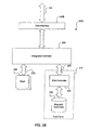
- FIG. 2B depicts an alternative embodiment 150B of the improved mass storage device.
- Logical interface 260 is eliminated and is replaced by a physical interface 275 directly to a flash memory array 280.
- Direct control of the flash memory array 280 is implemented by integrated controller 285, which can perform the functions of both storage controller 245 and router 235.
- the function of flash controller 220 is not required and flash memory array 280 does not form part of a logical data storage device, but is used directly as a physical store. It is particularly suited to temporary storage of streams of data.
- FIG. 3 depicts one way of organizing storage of sectors in a stream of data in flash memory array 280, in the form of a ring buffer 300.
- the current location for writing a sector of data is defined by a write pointer 305, which moves clockwise in FIG. 3 through the address space in an endless cycle.
- the address space is defined by metablocks (e. g. 310 and 315), which are linked (e. g. 320) either in a pre-set order or in an order dynamically determined when write pointer 305 moves from a full metablock to a new erased metablock.
- An erase pointer 325 similarly moves clockwise in FIG. 3 through the address space in an endless cycle.
- Metablocks identified by erase pointer 325 are erased at a rate that ensures that a small pool of erased metablocks is maintained ahead of write pointer 305, for storage of new data sectors. Blocks being erased contain the least recently written data in ring buffer 300.
- the improved mass storage device 150 can take advantage of its dual nature by using the flash memory system 205 as a read cache, which stores a copy of all data read from the magnetic hard drive 210.
- the flash memory system 205 may either have a region of its logical address space allocated as the read cache, or may be have its logical address space entirely devoted to the function.
- the location for storing cached data within the identified region of logical address space may be determined by an incrementing write address pointer defining a cyclic buffer, or may be a deterministic function of the logical address of the data within the magnetic hard drive 210.
- ring buffer 300 may be used to store a copy of all data read from the magnetic hard drive 210, at locations defined by the write pointer. Recently read data is, therefore, always present in the ring buffer 300, while older data is erased when its associated metablock is identified by the erase pointer.
- data being read from the disk device may be selectively copied to the read cache. This could be on the basis of the frequency with which the data is read, the nature of the file that is being read, or some other criterion.
- the improved mass storage device 150 can operate with its flash memory system 205 acting as a write cache.
- a cyclic buffer similar to one previously described for the read cache, can be used to store data supplied from the host bus 155 in parallel with its writing to the hard drive 210. In this manner, incoming data can be stored in the improved mass storage device 150, allowing the system 100 to complete its write operation sooner than would otherwise be possible if the only mass storage device was a single magnetic hard drive 210.
- the CPU 140 can act as if the data has reached its final destination, even though the improved mass storage device 150 still needs to complete the transfer of data from the flash memory system 205 to the magnetic hard drive 210.
- the transfer will typically occur when the mass storage device 150 is not otherwise being used. However, if the flash memory system 205 has the capability to read and write during a single cycle (e. g., using a dual port memory structure), the transfer can occur during the writing to flash memory system 205.
- the overall increase in system performance depends upon both the capacity of the flash memory system 205 and how often the improved mass storage device 150 is being accessed.
- a small capacity flash that does not qualify as a mass storage device would simply be the equivalent of a flash cache, and would not greatly improve the system performance.
- the system performance benefits get more drastic, as shown in FIG. 4A .
- FIG. 4B shows that as the improved mass storage device 150 becomes more utilized, the system performance degrades. If the mass storage device 150 is constantly accessed, there will not be enough time to transfer the data from the flash memory system 205 to the hard drive 210. Eventually, the mass storage device 150 must stop using the flash memory system 205 and exclusively use the hard drive 210. If that happens, the system performance would be identical to a system that only used a hard drive 210.
- the improved mass storage device 150 should have an error handling routine that enables data to be directed to the hard drive 210 while bypassing the flash memory system 205. If the flash memory system 205 becomes full, the improved mass storage device 150 cannot simply overwrite the flash memory system 205 until the data is successfully transferred to the hard drive 210. The same error handling routine could also be utilized if the flash memory system 205 is temporarily not available (e. g., the flash memory system 205 is engaged in a garbage collection process).
- the write cache may exist independently of the read cache, occupying either a portion of the logical address space or the entire logical address space of the flash memory system 205, or it may coexist with the read cache.
- Another manner in which the improved mass storage device 150 can operate is by exclusively using the flash memory system 205 in certain situations. For example, in some cases it might be desirable for a system to enter into a portable mode where the hard drive 210, which is more susceptible to shock, becomes unavailable. Unavailability might simply mean that data is not sent to the hard drive 210, that the hard drive 210 is shut off in order to conserve power, or that the hard drive 210 is physically removed from the improved mass storage device 150. If, for example, the hard drive 210 were part of a docking station for a portable device, then removing the portable device from the docking station would make the hard drive 210 unavailable.
- the storage controller 245 would cause the two mass storage devices 205 and 210 to synchronize with each other.
- the hard drive 210 would become available once the portable device was put back in its docking station.
- the hard drive 210 might become available because motion detection circuitry determines that the system is no longer in danger of experiencing shock.
- the user might cause the system to place the hard drive 210 into an available state by manually changing its mode, or perhaps plugging the system into an electrical outlet.
- the system might simply re-active the hard drive 210 on its own in order to free up space in the flash memory system 205.
- the flash memory system 205 can act as a temporary back-up since data exists in the flash memory system 205 until overwritten with new data.
- Read caching, write caching, and exclusive storage can all be incorporated into the same device.
- the logical address space for the flash memory system 205 is a subset of the logical address space for the hard drive 210.
- the data request is associated with a single logical address.
- the most recent data that corresponds with that logical address can exist in the flash memory system 205, the hard drive 210, or both.
- the portion of the flash memory system dedicated to a certain operation might change depending upon the situation. For example, if the hard drive 210 is physically unavailable during exclusive storage mode, there is no need to dedicate any of the flash memory system 205 to the caching operations during that mode. Once docked, the system could then revert to using the flash memory system 205 for cache purposes (read, write or both).
Abstract
Description
- The present invention relates generally to data storage devices, and more specifically to dual media storage devices.
- General-purpose computers require a mass storage system. Unlike main memory, which is used for the direct manipulation of data, mass storage is used to retain data. Generally a program is stored in mass storage and, when the program is executed, either the entire program or portions of the program are copied into main memory. The speed at which a system is able to locate and transfer the program and its associated data from the mass storage device into the main memory is integral to the overall speed of a system.
- Common mass storage devices include floppy disks, hard disks, optical discs and tapes. Each device has both strengths and weaknesses, which can relate to capacity, price, speed and portability.
- Additionally, other devices, such as flash memory, can provide non- volatile storage. Flash memory is a type of electrically erasable programmable read- only memory (EEPROM). Although flash memory is typically not as fast as the volatile main memory, it is faster than hard disks.
- The inventor has previously explored the concept of merging separate devices into a single mass storage system in order to maximize each device's strengths and minimize each device's weaknesses. For example, the inventor was also identified as the inventor for PCT application "Memory Device"
WO 97/50035 U. S. Pat. No. 6,016, 530, issued to Daniel Auclair and Eliyahou Harari on January 18, 2000 . - By combining a non-volatile flash memory device with a non-volatile hard disk, a resulting mass storage system can be greater than the sum of its parts. However, such memory system was specifically limited to a situation where only one version of each data sector was ever maintained. The data sector was stored in either the high-speed memory or in the slow-access mass data storage device, making the logical address space equal to the sum of the capacities of the high-speed memory and the slow-access mass storage device.
- There are many commercially successful non-volatile memory products being used today that employ an array of flash cells formed on one or more integrated circuits chips. A memory controller, usually (but not necessarily) on a separate integrated circuit chip, controls operation of the memory array. Such a controller typically includes a microprocessor, some non-volatile read-only memory (ROM), a volatile random-access memory (RAM) and one or more special circuits such as one that calculates an error-correction-code (ECC) from data as it passes through the controller during programming and reading operations.
- Memory cells of a typical flash array are divided into discrete blocks of cells that are erased together. That is, the erase block is the erase unit--a minimum number of cells that are simultaneously erasable. Each erase block typically stores one or more pages of data, the page programmed or read in parallel in different sub- arrays or planes. Each planes typically stores one or more sectors of data, the size of the sector being defined by the host system. An example sector includes 512 bytes of user data, following a standard established with magnetic disk drives. Such memories are typically configured with 16, 32 or more pages within each erase black, and each page stores one or just a few host sectors of data.
- In order to increase the degree of parallelism during programming and reading operations the array is typically divided into sub-arrays, commonly referred to as planes. Each plane can contain its own data registers and other circuits to allow parallel operation such that the sectors of data may be programmed to or read from all the planes simultaneously. An array on a single integrated circuit may be physically divided into planes, or each plane may be formed from a separate one or more integrated circuit chips. Examples of such a memory implementation are described in
U. S. Patent No. 5,798, 968 , "Plane decode/virtual sector architecture," issued to Lee et al. on August 25, 1998, andU. S. Patent No. 5,890, 192 , "Concurrent write of multiple chunks of data into multiple subarrays of flash EEPROM," issued to Lee et al. on March 30, 1999. - To further efficiently manage the memory, erase blocks may be linked together to form virtual blocks or metablocks. That is, each metablock is defined to include one erase block from each plane. Use of the metablock is described in international patent application "Partial Block Data Programming And Reading Operations In A Non-Volatile Memory," publication no.:
W002/058074 on July 25, 2002 - Flash memory systems of this type are commonly used as mass storage devices in portable applications. The flash memory device communicates with a host system via a logical interface using a protocol such as ATA, and is frequently in the form of a removable card. Some of the commercially available cards are CompactFlash™ (CF) cards, MultiMedia cards (MMC), Secure Digital (SD) cards, Smart Media cards, personnel tags (P-Tag) and Memory Stick cards. Hosts include personal computers, notebook computers, personal digital assistants (PDAs), various data communication systems, and similar types of equipment. Besides the memory card implementation, this type of memory can alternatively be embedded into various types of host systems.
- In the past, flash memory has been used for various data caching functions, for storage of a computer's BIOS, or as an extension of a mass storage device (as in the above PCT application). It has been used within a hard disk device for caching write or read data. For example,
U. S. Patent No. 5,586, 291 , "Disk controller with volatile and non-volatile cache memories," to Lasker et al. on December 17, 1996 describes the use of a non-volatile memory as a write cache for a hard disk, with data mirrored in a volatile memory that acts as a read cache.U. S. Patents 5,636, 355 , "Disk cache management techniques using non-volatile storage," to Ramakrishnan et al. on June 3, 1997, and5,542, 066 , "Destaging modified data blocks from cache memory," to Mattson et al. on July 30, 1996, also describe use on non-volatile memory as a write cache for a hard disk, and purging or destaging algorithms for moving data from the cache to the hard disk. In known applications of non-volatile memory as a disk cache, data identified by a logical address in the hard drive is temporarily mapped to a physical location in the non-volatile memory. - There are continuing efforts to improve mass storage devices.
- According to a first aspect of the present invention there is provided a method of improving the performance of a first mass storage device in a computer system, comprising: connecting the first mass storage device to a system bus in the computer system through a first interface allowing data to be passed in either direction between the bus and the first mass storage device; connecting a second mass storage device with faster access time and lower capacity to the system bus through a second interface allowing data to be passed in either direction between the bus and the second mass storage device; and using a storage controller to satisfy data requests from the computer system with data that is stored in the second mass storage device or, if the requested data is not present in the second mass storage device, with data that is stored in the first mass storage device.
- According to a second aspect of the present invention there is provided a computer system, comprising: a first mass storage device; a second mass storage device, the second mass storage device having faster access time and lower capacity than the first mass storage device; a system bus, the first mass storage device connected to the system bus through a first interface that allows data to be passed in either direction between the system bus and the first mass storage device, and the second mass storage device connected to the system bus through a second interface allowing data to be passed in either direction between the bus and the second mass storage device; and a storage controller connected to the system bus, the storage controller used to satisfy data requests from the computer system with data that is stored in the second mass storage device and with data that is stored in the first mass storage device when the requested data is not present in the second mass storage device.
- According to a third aspect of the present invention there is provided a memory controller, the memory controller arranged to improve the performance of a first mass storage device in a computer system, comprising: the memory controller connected to a system bus, the system bus connected to: the first mass storage device to through a first interface that allows data to be passed in either direction between the system bus and the first mass storage device, and a second mass storage device through a second interface that allows data to be passed in either direction between the system bus and the second mass storage device, the second mass storage device having faster access time and lower capacity than the first mass storage device, wherein the storage controller satisfies data requests from the computer system with data that is stored in the second mass storage device and with data that is stored in the first mass storage device when the requested data is not present in the second mass storage device.
- According to a fourth aspect of the present invention there is provided a non-transitory computer readable medium for storing computer code executable by a processor for improving the performance of a first mass storage device in a computer system, comprising: computer code for connecting the first mass storage device to a system bus in the computer system through a first interface allowing data to be passed in either direction between the bus and the first mass storage device; computer code for connecting a second mass storage device with faster access time and lower capacity to the system bus through a second interface allowing data to be passed in either direction between the bus and the second mass storage device; and computer code for using a storage controller to satisfy data requests from the computer system with data that is stored in the second mass storage device or, if the requested data is not present in the second mass storage device, with data that is stored in the first mass storage device.
- The second mass storage device may act as a cache memory to the first mass storage device.
- The second mass storage device may be a semiconductor memory and wherein the first mass storage device is a hard drive.
- Embodiments of the present invention provide a data storage system that can include two non-volatile mass storage devices and a storage controller. The second non-volatile mass storage device has a faster access time and a lower capacity than the first non- volatile mass storage device. The two non-volatile mass storage devices have overlapping address ranges. In other words, any piece of data might be simultaneously available on both mass storage devices.
- In one embodiment, the first non-volatile mass storage device can be placed in an available state and an unavailable state. When the first mass storage device is in its unavailable state, the storage controller only accesses the second mass storage device. An unavailable state might mean the device is physically unavailable (e. g., removed) or simply that the storage controller simply will not access it until it is placed back in an available state. When the first mass storage device is in the available state, the storage controller is operable to access either the first mass storage device or the second mass storage device.
- In another embodiment, the storage controller directs incoming data into either the first non-volatile mass storage device or the second non-volatile mass storage device. If data is directed into the second mass storage device, then the data is later copied from the second mass storage device into the first mass storage device. The storage controller's choice of which non-volatile mass storage device to direct incoming data into is at least partially dependant upon the amount of data in the second non-volatile mass storage device that has not been copied into the first non- volatile storage device.
- In another embodiment, the storage controller satisfies external data requests with data that is stored in either the second non-volatile mass storage device or, if the requested data is not present in the second non-volatile mass storage device, with data that is stored in the first non-volatile mass storage device.
- In one embodiment, a data storage system comprises a first non-volatile mass storage device that can be placed in an available state and an unavailable state and having a first range of logical addresses; a second non-volatile mass storage device having a faster access time and a lower capacity than the first non-volatile mass storage device and having a second range of logical addresses; and a storage controller that can access data within the second non-volatile mass storage device when the first non-volatile mass storage device is in the unavailable state and operable to access data within both the first and second non-volatile mass storage devices when the first non-volatile mass storage device is in the available state; wherein the first range of logical addresses and the second range of logical addresses are overlapping with each other.
- The unavailable state may be activated when the data storage system enters a portable mode.
- The portable mode may be determined with motion detection circuitry.
- A portion of the second range of logical addresses may be non-overlapping with the first range of addresses, whereby the portion of the second range of addresses contains data that does not also reside on the first non-volatile mass storage device.
- The storage controller may synchronize the data contained in the second range of addresses on the second non- volatile mass storage device with the first range of addresses on the first non-volatile mass storage device after the first non-volatile mass storage device transitions out of the unavailable state to the available state.
- The second non-volatile mass storage device may be capable of acting as a cache for the first non-volatile mass storage device when the first non-volatile mass storage device is in the available state.
- The first non-volatile mass storage device may use a magnetic hard disk to store data and the second non-volatile mass storage device uses a flash memory array to store data.
- In a further embodiment, a data storage system may comprise: a first non-volatile mass storage device that has a first range of logical addresses; a second non-volatile mass storage device having a faster access time and a lower capacity than the first non-volatile mass storage device and having a second range of logical addresses, the first range of logical addresses and the second range of logical addresses overlapping with each other; and a storage controller that directs incoming data into either the first non-volatile mass storage device or the second non-volatile mass storage device; wherein after data has been directed into the second non-volatile mass storage device, the data is copied from the second non-volatile mass storage device into the first non-volatile mass storage device; and wherein the storage controller's choice of which non-volatile mass storage device to direct incoming data into is at least partially dependant upon the amount of data in the second non-volatile mass storage device that has not been copied into the first non-volatile storage device.
- Data may be copied from the second non-volatile mass storage device into the first non-volatile mass storage device during periods of inactivity.
- The second non-volatile mass storage device may experience periods of inaccessibility; and the storage controller may direct data into the first non-volatile mass storage device when the second non-volatile mass storage device is in a period of inaccessibility.
- The periods of inaccessibility may be caused, at least in part, by garbage collection operations.
- Data in the second non-volatile mass storage device may be stored in a cyclic buffer arrangement.
- The first non-volatile mass storage device may use a magnetic hard disk to store data and the second non-volatile mass storage device uses a flash memory array to store data.
- In a further embodiment, a data storage system comprises: a first non-volatile mass storage device that has a first range of logical addresses; a second non-volatile mass storage device having a faster access time and a lower capacity than the first storage device and having a second range of logical addresses, the first range of logical addresses and the second range of logical addresses overlapping with each other; and a storage controller that satisfies data requests with data that is stored in the second non-volatile mass storage device or, if the requested data is not present in the second non-volatile mass storage device, with data that is stored in the first non- volatile mass storage device.
- Data may be copied from the first non- volatile mass storage device to the second non-volatile mass storage device according to frequency with which the data is read.
- Data may be copied from the first non- volatile mass storage device to the second non-volatile mass storage device according to the nature of the data that is being read.
- Data in the second non-volatile mass storage device may be stored in a cyclic buffer arrangement.
- The first non-volatile mass storage device may use a magnetic hard disk to store data and the second non-volatile mass storage device uses a flash memory array to store data.
- Other aspects and advantages of the invention will become apparent from the following detailed description taken in conjunction with the accompanying drawings which illustrate, by way of example, the principles of the invention.
- The invention may best be understood by reference to the following description taken in conjunction with the accompanying drawings, in which:
-
FIG. 1A depicts an exemplary general-purpose computer system that can utilize the invention; -
FIG. 1B depicts an abstracted representation of the general-purpose computer system ofFIG. 1A ; -
FIG. 2A depicts the improved mass storage device according to an exemplary embodiment of the present invention; -
FIG. 2B depicts the improved mass storage device according to another exemplary embodiment of the present invention; -
FIG. 3 depicts a stylized representation of a ring buffer; -
FIG. 4A depicts a graph illustrating system performance benefits as flash capacity increases; and -
FIG. 4B depicts a graph illustrating system performance benefits as utilization of the improved mass storage device decreases. - It is to be understood that, in the drawings, like reference numerals designate like structural elements. Also, it is understood that the depictions in the FIGs. are not necessarily to scale.
- In the following description, numerous specific details are set forth to provide a thorough understanding of the present invention. However, it will be apparent to one skilled in the art that the present invention may be practiced without some or all of these specific details. In other instances, well known process steps have not been described in detail in order to avoid unnecessarily obscuring the present invention.
- The present invention generally improves upon prior mass storage devices, also commonly called auxiliary memory, by combining two separate mass storage devices, each having its own strengths and weaknesses. For example when a flash mass storage device ("flash memory system") is compared to a hard drive, the flash memory system is more resistant to shock and more desirable for portable applications because it can operate without moving parts. Although the flash memory system has a faster access time than a hard drive, it generally does not have the storage capacity of an equivalently priced hard drive. Additionally, the flash memory system typically requires periodic garbage collection operations performed that renders the flash memory system inaccessible for a period of time. The improved mass storage device of the present invention uses either a flash memory system or a hard drive depending upon which device is more suitable for a certain circumstance. As will be appreciate by those skilled in the art, any two non-volatile mass storage devices can be used in the present invention as long as one has a faster access time and a lower capacity than the other.
- Several different advantages can be gained with the improved mass storage device. In one embodiment, the improved mass storage device can provide for fast system boot and fast application start-up. Information required by a host system during its boot process, such as operating system and configuration files, can be stored in the flash memory system, with a second copy optionally being stored in the hard drive. In such a system, the flash memory system can be used as a non-volatile read cache, and its fast random read access characteristics allow much faster system start-up. This information can initially be identified as being frequently read information and can be copied to the flash memory system during its initial access from the hard drive. Such information can be protected to prevent it being overwritten by other applications that use the flash memory system in the mass storage device. Application software files can be treated in the same way to provide fast start-up of applications.
- In another embodiment, the improved mass storage device can act as a low-power storage device. The improved mass storage device can use the flash memory system as a read/write cache by maintaining a copy of recently accessed information in the flash memory system, together with a copy of recently written information. The device can then spin down the magnetic hard disk to reduce power in portable applications and take advantage of the low power characteristics of flash memory, while retaining a high probability of fast response for required information by means of a cache hit in flash memory.
- Similarly, the improved mass storage device can also provide the advantage of being a shock-tolerant storage device. Spinning down the magnetic hard disk when in an environment with a risk of high mechanical shock, would take advantage of the high shock tolerance of semiconductor memory, while retaining an operating capability with the information stored in the flash memory system.
- Yet another potential advantage of the improved mass storage device is its ability to provide a highly reliable storage device with short-term backup. If the flash memory system maintains recently written information in the flash memory system as a write cache, the information is retained in the flash memory system even after it is transferred to the hard drive. If the information is maintained for as long as possible, and is only overwritten when space is required, then the write cache provides the security of a second copy of recently written information. The improved mass storage device can, therefore, result in a reliable storage device that uses the high shock tolerance of semiconductor memory to protect against loss, due to mechanical failure such as a disk crash, of recently written information that has not yet been backed up.
-
FIG. 1A depicts an exemplary general-purpose computer system 100 that can utilize the current invention. Components include acomputer 105, various input devices such as amouse 110 andkeyboard 115, and various output devices such as amonitor 120 and aprinter 125. -
FIG. 1B depicts an abstracted representation of acomputer system 100 ofFIG. 1A that depicts its essential components. Asingle component 130 represents input devices that allow a user to interact with thecomputer system 100, such as a mouse and keyboard. Similarly, asingle component 135 represents the output devices that display what thecomputer system 100 has accomplished, such as a monitor and printer. The heart of thecomputer system 100 is a central processing unit (CPU) 140, and is the component that executes instructions.Main memory 145 is typically volatile and provides theCPU 140 with both the instructions to be executed and data to be manipulated by the instructions. These components 130,135, 140, and 145 are all well known in the art. - An improved
mass storage device 150 allows thecomputer system 100 to permanently retain large amounts of data. The components 130,135, 140,145, and 150 are able to exchange information with each other via ahost bus 155. -
FIG. 2A depicts an improvedmass storage device 150A according to an exemplary embodiment of the present invention. Two mass storage devices, aflash memory system 205 and ahard drive 210 are connected in parallel. Theflash memory system 205 includes aflash memory array 215 and aflash controller 220. Thehard drive 210 includes a magnetichard disk 225 and adisk controller 230. Eachcontroller flash controller 220 controls all logical-to-physical mapping of data sectors and all flash memory management such that theinterface 250 between theflash controller 220 and theflash memory array 215 is a physical interface. Thedisk controller 230 manages operation of the magnetichard disk 225 for reading and writing. Bothcontrollers router 235 vialogical interfaces - In another embodiment, the functions of the
controllers router 235, in an integrated controller device. This device may also includestorage controller 245 andhost interface 240. However, such a configuration would require the production of new controller units. Accordingly, either one or both of thecontrollers - In
FIG. 2A , ahost interface 240 and astorage controller 245 are both positioned upstream from therouter 235, which allows data and control information to be passed in either direction between thehost interface 240 and either thedisk controller 230 or theflash controller 220. Additionally, therouter 235 can control transfer of data in either direction between thedisk controller 230 and theflash controller 220. Such transfers can be done as a stand-alone operation. Alternatively, such transfers can be done in conjunction with a data transfer in either direction between thehost interface 240 and one of themass storage controllers router 235 can incorporate control logic for such data transfers. - The
host interface 240 provides a direct interface to thehost bus 155, and can provide all support for the specific protocol in use on thehost bus 155. The subsystem formed by thehost interface 240, thedisk controller 230 and the magnetichard disk 225 as well as the subsystem formed by thehost interface 240, theflash controller 220 and theflash memory array 215 both form complete mass data storage systems. Therouter 235 may pass data and control signals without modification from thehost interface 240, or may establish an alternative protocol for communication with thecontrollers Interfaces router 235 and themass storage controllers mass storage device 150.Interfaces flash memory system 205 andhard drive 210 and are not dependent on the physical characteristics of the respective storage media. - In addition, the
flash controller 220 might also support special commands or operations oninterface 260 to give direct access to reserved areas of theflash memory array 215, which can be used for storage of tables and information logs used by thestorage controller 245. Alternatively, thestorage controller 245 might have its own non-volatile memory for such tables and logs. - The
storage controller 245 is an intelligent control unit that directs the transfer of information between thehost interface 240 and themass storage controllers storage controller 245 coordinates the storage of data to or reading of data from theflash memory system 205 or thehard drive 210. Thestorage controller 245 maintains address tables for information stored in theflash memory array 215 and, in some embodiments, the magnetichard disk 225 as well. - Volatile memory might act as a buffer or cache memory in many of the components of the improved
mass storage device 150, including thehost interface 240, therouter 235, theflash controller 220 or thedisk controller 230. Either a single volatile memory may be scheduled to operate in the various components, or separate volatile memories can be dedicated to each component. -
FIG. 2B depicts analternative embodiment 150B of the improved mass storage device.Logical interface 260 is eliminated and is replaced by aphysical interface 275 directly to aflash memory array 280. Direct control of theflash memory array 280 is implemented byintegrated controller 285, which can perform the functions of bothstorage controller 245 androuter 235. In this embodiment, the function offlash controller 220 is not required andflash memory array 280 does not form part of a logical data storage device, but is used directly as a physical store. It is particularly suited to temporary storage of streams of data. -
FIG. 3 depicts one way of organizing storage of sectors in a stream of data inflash memory array 280, in the form of aring buffer 300. The current location for writing a sector of data is defined by awrite pointer 305, which moves clockwise inFIG. 3 through the address space in an endless cycle. The address space is defined by metablocks (e. g. 310 and 315), which are linked (e. g. 320) either in a pre-set order or in an order dynamically determined whenwrite pointer 305 moves from a full metablock to a new erased metablock. An erasepointer 325 similarly moves clockwise inFIG. 3 through the address space in an endless cycle. Metablocks identified by erasepointer 325 are erased at a rate that ensures that a small pool of erased metablocks is maintained ahead ofwrite pointer 305, for storage of new data sectors. Blocks being erased contain the least recently written data inring buffer 300. - The improved
mass storage device 150 can take advantage of its dual nature by using theflash memory system 205 as a read cache, which stores a copy of all data read from the magnetichard drive 210. Theflash memory system 205 may either have a region of its logical address space allocated as the read cache, or may be have its logical address space entirely devoted to the function. The location for storing cached data within the identified region of logical address space may be determined by an incrementing write address pointer defining a cyclic buffer, or may be a deterministic function of the logical address of the data within the magnetichard drive 210. - Alternatively, in
mass storage device 150B,ring buffer 300 may be used to store a copy of all data read from the magnetichard drive 210, at locations defined by the write pointer. Recently read data is, therefore, always present in thering buffer 300, while older data is erased when its associated metablock is identified by the erase pointer. - Alternatively, data being read from the disk device may be selectively copied to the read cache. This could be on the basis of the frequency with which the data is read, the nature of the file that is being read, or some other criterion.
- In another embodiment, the improved
mass storage device 150 can operate with itsflash memory system 205 acting as a write cache. A cyclic buffer, similar to one previously described for the read cache, can be used to store data supplied from thehost bus 155 in parallel with its writing to thehard drive 210. In this manner, incoming data can be stored in the improvedmass storage device 150, allowing thesystem 100 to complete its write operation sooner than would otherwise be possible if the only mass storage device was a single magnetichard drive 210. When data stops being sent over thehost system bus 155, theCPU 140 can act as if the data has reached its final destination, even though the improvedmass storage device 150 still needs to complete the transfer of data from theflash memory system 205 to the magnetichard drive 210. The transfer will typically occur when themass storage device 150 is not otherwise being used. However, if theflash memory system 205 has the capability to read and write during a single cycle (e. g., using a dual port memory structure), the transfer can occur during the writing toflash memory system 205. - The overall increase in system performance depends upon both the capacity of the
flash memory system 205 and how often the improvedmass storage device 150 is being accessed. A small capacity flash that does not qualify as a mass storage device would simply be the equivalent of a flash cache, and would not greatly improve the system performance. However, as the flash gets bigger, the system performance benefits get more drastic, as shown inFIG. 4A . The bigger theflash memory system 205, the more data can be stored during a burst of activity. - Similarly,
FIG. 4B shows that as the improvedmass storage device 150 becomes more utilized, the system performance degrades. If themass storage device 150 is constantly accessed, there will not be enough time to transfer the data from theflash memory system 205 to thehard drive 210. Eventually, themass storage device 150 must stop using theflash memory system 205 and exclusively use thehard drive 210. If that happens, the system performance would be identical to a system that only used ahard drive 210. - As will be appreciated by those skilled in the art, the improved
mass storage device 150 should have an error handling routine that enables data to be directed to thehard drive 210 while bypassing theflash memory system 205. If theflash memory system 205 becomes full, the improvedmass storage device 150 cannot simply overwrite theflash memory system 205 until the data is successfully transferred to thehard drive 210. The same error handling routine could also be utilized if theflash memory system 205 is temporarily not available (e. g., theflash memory system 205 is engaged in a garbage collection process). - The write cache may exist independently of the read cache, occupying either a portion of the logical address space or the entire logical address space of the
flash memory system 205, or it may coexist with the read cache. - Another manner in which the improved
mass storage device 150 can operate is by exclusively using theflash memory system 205 in certain situations. For example, in some cases it might be desirable for a system to enter into a portable mode where thehard drive 210, which is more susceptible to shock, becomes unavailable. Unavailability might simply mean that data is not sent to thehard drive 210, that thehard drive 210 is shut off in order to conserve power, or that thehard drive 210 is physically removed from the improvedmass storage device 150. If, for example, thehard drive 210 were part of a docking station for a portable device, then removing the portable device from the docking station would make thehard drive 210 unavailable. - Once the
hard drive 210 became available again, thestorage controller 245 would cause the twomass storage devices hard drive 210 would become available once the portable device was put back in its docking station. In other circumstances, thehard drive 210 might become available because motion detection circuitry determines that the system is no longer in danger of experiencing shock. In yet other circumstances, the user might cause the system to place thehard drive 210 into an available state by manually changing its mode, or perhaps plugging the system into an electrical outlet. In yet other circumstances, the system might simply re-active thehard drive 210 on its own in order to free up space in theflash memory system 205. In all cases, theflash memory system 205 can act as a temporary back-up since data exists in theflash memory system 205 until overwritten with new data. - Read caching, write caching, and exclusive storage can all be incorporated into the same device. In each situation the logical address space for the
flash memory system 205 is a subset of the logical address space for thehard drive 210. In other words, when a data request comes from thehost bus 155, the data request is associated with a single logical address. The most recent data that corresponds with that logical address can exist in theflash memory system 205, thehard drive 210, or both. - In some embodiments the portion of the flash memory system dedicated to a certain operation might change depending upon the situation. For example, if the
hard drive 210 is physically unavailable during exclusive storage mode, there is no need to dedicate any of theflash memory system 205 to the caching operations during that mode. Once docked, the system could then revert to using theflash memory system 205 for cache purposes (read, write or both). - Although the invention has been described in its presently contemplated best mode, it is clear that it is susceptible to numerous modifications, modes of operation and embodiments, all within the ability and skill of those familiar with the art and without exercise of further inventive activity. For example, if certain programs are better suited to being permanently stored in the flash memory system, then no corresponding logical address would need be stored in the hard drive for those programs. Furthermore, other mass storage devices might use technology other than either flash or hard drives, and might include battery backed RAM, optical disks, ovonics unified memory (OUM), magnetic RAM (MRAM), ferroelectric polymer, ferroelectric RAM (FeRAM), silicon on insulator (SoI), etc.
Claims (12)
- A method of improving the performance of a first mass storage device (210) in a computer system, comprising:connecting the first mass storage device (210) to a system bus in the computer system through a first interface allowing data to be passed in either direction between the bus and the first mass storage device (210);connecting a second mass storage device (280) with faster access time and lower capacity to the system bus through a second interface allowing data to be passed in either direction between the bus and the second mass storage device (280); andusing a storage controller (285) to satisfy data requests from the computer system with data that is stored in the second mass storage device (280) or, if the requested data is not present in the second mass storage device (280), with data that is stored in the first mass storage device (210).
- The method as recited in claim 1, wherein the second mass storage device (280) acts as a cache memory to the first mass storage device (210).
- The method as recited in claim 2, wherein the second mass storage device (280) is a semiconductor memory and wherein the first mass storage device (210) is a hard drive.
- A computer system, comprising:a first mass storage device (210);
a second mass storage device (280), the second mass storage device (280) having faster access time and lower capacity than the first mass storage device (210);
a system bus, the first mass storage device (210) connected to the system bus through a first interface that allows data to be passed in either direction between the system bus and
the first mass storage device (210), and the second mass storage device (280) connected to the system bus through a second interface allowing data to be passed in either direction between the bus and the second mass storage device (280); anda storage controller (285) connected to the system bus, the storage controller (285) used to satisfy data requests from the computer system with data that is stored in the second mass storage device (280) and with data that is stored in the first mass storage device (210) when the requested data is not present in the second mass storage device (280). - The system as recited in claim 4, wherein the second mass storage device (280) acts as a cache memory to the first mass storage device (210).
- The system as recited in claim 5, wherein the second mass storage device (280) is a semiconductor memory and wherein the first mass storage device (210) is a hard drive.
- A memory controller, the memory controller arranged to improve the performance of a first mass storage device (210) in a computer system, comprising:the memory controller connected to a system bus, the system bus connected to: the first mass storage device (210) to through a first interface that allows data to be passed in either direction between the system bus and the first mass storage device (210), anda second mass storage device (280) through a second interface that allows data to be passed in either direction between the system bus and the second mass storage device (280), the second mass storage device (280) having faster access time and lower capacity than the first mass storage device (210), wherein the storage controller (285) satisfies data requests from the computer system with data that is stored in the second mass storage device (280) and with data that is stored in the first mass storage device (210) when the requested data is not present in the second mass storage device (280).
- The memory controller as recited in claim 7, wherein the second mass storage device (280) acts as a cache memory to the first mass storage device (210).
- The memory controller as recited in claim 8, wherein the second mass storage device (280) is a semiconductor memory and wherein the first mass storage device (210) is a hard drive.
- Non-transitory computer readable medium for storing computer code executable by a processor for improving the performance of a first mass storage device (210) in a computer system, comprising:computer code for connecting the first mass storage device (210) to a system bus in the computer system through a first interface allowing data to be passed in either direction between the bus and the first mass storage device (210);computer code for connecting a second mass storage device (280) with faster access time and lower capacity to the system bus through a second interface allowing data to be passed in either direction between the bus and the second mass storage device (280); andcomputer code for using a storage controller (285) to satisfy data requests from the computer system with data that is stored in the second mass storage device (280) or, if the requested data is not present in the second mass storage device (280), with data that is stored in the first mass storage device (210).
- The computer readable medium as recited in claim 10, wherein the second mass storage device (280) acts as a cache memory to the first mass storage device (210).
- The computer readable medium as recited in claim 11, wherein the second mass storage device (280) is a semiconductor memory and wherein the first mass storage device (210) is a hard drive.
Applications Claiming Priority (2)
| Application Number | Priority Date | Filing Date | Title |
|---|---|---|---|
| US10/772,855 US7136973B2 (en) | 2004-02-04 | 2004-02-04 | Dual media storage device |
| EP04815868A EP1711883A1 (en) | 2004-02-04 | 2004-12-28 | Dual media storage device |
Related Parent Applications (1)
| Application Number | Title | Priority Date | Filing Date |
|---|---|---|---|
| EP04815868.7 Division | 2004-12-28 |
Publications (1)
| Publication Number | Publication Date |
|---|---|
| EP2254022A1 true EP2254022A1 (en) | 2010-11-24 |
Family
ID=34808629
Family Applications (2)
| Application Number | Title | Priority Date | Filing Date |
|---|---|---|---|
| EP04815868A Withdrawn EP1711883A1 (en) | 2004-02-04 | 2004-12-28 | Dual media storage device |
| EP10174703A Withdrawn EP2254022A1 (en) | 2004-02-04 | 2004-12-28 | Dual media storage device |
Family Applications Before (1)
| Application Number | Title | Priority Date | Filing Date |
|---|---|---|---|
| EP04815868A Withdrawn EP1711883A1 (en) | 2004-02-04 | 2004-12-28 | Dual media storage device |
Country Status (9)
| Country | Link |
|---|---|
| US (2) | US7136973B2 (en) |
| EP (2) | EP1711883A1 (en) |
| JP (2) | JP5129484B2 (en) |
| KR (1) | KR101105955B1 (en) |
| CN (1) | CN100487632C (en) |
| AU (1) | AU2005200321A1 (en) |
| CA (1) | CA2492921C (en) |
| TW (1) | TWI380171B (en) |
| WO (1) | WO2005081093A1 (en) |
Cited By (1)
| Publication number | Priority date | Publication date | Assignee | Title |
|---|---|---|---|---|
| WO2014193404A1 (en) * | 2013-05-31 | 2014-12-04 | Hewlett-Packard Development Company, L.P. | Mass storage device |
Families Citing this family (135)
| Publication number | Priority date | Publication date | Assignee | Title |
|---|---|---|---|---|
| US7108975B2 (en) * | 2001-09-21 | 2006-09-19 | Regents Of The University Of Michigan | Atlastin |
| US20050216679A1 (en) * | 2004-03-25 | 2005-09-29 | Itzhak Levy | Hard disk automatic hardware-based scheduled archiving |
| US7634615B2 (en) * | 2004-06-10 | 2009-12-15 | Marvell World Trade Ltd. | Adaptive storage system |
| US7788427B1 (en) | 2005-05-05 | 2010-08-31 | Marvell International Ltd. | Flash memory interface for disk drive |
| US7730335B2 (en) | 2004-06-10 | 2010-06-01 | Marvell World Trade Ltd. | Low power computer with main and auxiliary processors |
| US7617359B2 (en) * | 2004-06-10 | 2009-11-10 | Marvell World Trade Ltd. | Adaptive storage system including hard disk drive with flash interface |
| US20080140921A1 (en) * | 2004-06-10 | 2008-06-12 | Sehat Sutardja | Externally removable non-volatile semiconductor memory module for hard disk drives |
| US7702848B2 (en) * | 2004-06-10 | 2010-04-20 | Marvell World Trade Ltd. | Adaptive storage system including hard disk drive with flash interface |
| US20070083785A1 (en) * | 2004-06-10 | 2007-04-12 | Sehat Sutardja | System with high power and low power processors and thread transfer |
| US20070094444A1 (en) * | 2004-06-10 | 2007-04-26 | Sehat Sutardja | System with high power and low power processors and thread transfer |
| JP4311287B2 (en) * | 2004-06-25 | 2009-08-12 | ソニー株式会社 | Boot system, boot method, and data processing apparatus using the boot method |
| US7472222B2 (en) * | 2004-10-12 | 2008-12-30 | Hitachi Global Storage Technologies Netherlands B.V. | HDD having both DRAM and flash memory |
| JP2006146460A (en) * | 2004-11-18 | 2006-06-08 | Sony Corp | Communication system, storage device and controller |
| CN100456265C (en) * | 2004-12-14 | 2009-01-28 | 国际商业机器公司 | System and method of operating a mobile computer system |
| US7933172B2 (en) * | 2005-01-10 | 2011-04-26 | Hewlett-Packard Development Company, L.P. | Method for playing contents using master and slave optical disc |
| US9104315B2 (en) | 2005-02-04 | 2015-08-11 | Sandisk Technologies Inc. | Systems and methods for a mass data storage system having a file-based interface to a host and a non-file-based interface to secondary storage |
| US7610445B1 (en) * | 2005-07-18 | 2009-10-27 | Palm, Inc. | System and method for improving data integrity and memory performance using non-volatile media |
| JP5008845B2 (en) * | 2005-09-01 | 2012-08-22 | 株式会社日立製作所 | Storage system, storage apparatus and control method thereof |
| US8291295B2 (en) | 2005-09-26 | 2012-10-16 | Sandisk Il Ltd. | NAND flash memory controller exporting a NAND interface |
| US7631245B2 (en) | 2005-09-26 | 2009-12-08 | Sandisk Il Ltd. | NAND flash memory controller exporting a NAND interface |
| US20070106842A1 (en) * | 2005-11-04 | 2007-05-10 | Conley Kevin M | Enhanced first level storage caching methods using nonvolatile memory |
| US7634585B2 (en) | 2005-11-04 | 2009-12-15 | Sandisk Corporation | In-line cache using nonvolatile memory between host and disk device |
| US7747837B2 (en) | 2005-12-21 | 2010-06-29 | Sandisk Corporation | Method and system for accessing non-volatile storage devices |
| US7769978B2 (en) | 2005-12-21 | 2010-08-03 | Sandisk Corporation | Method and system for accessing non-volatile storage devices |
| US7793068B2 (en) | 2005-12-21 | 2010-09-07 | Sandisk Corporation | Dual mode access for non-volatile storage devices |
| KR100755702B1 (en) * | 2005-12-27 | 2007-09-05 | 삼성전자주식회사 | Storage apparatus using non volatile memory as cache and method for operating the same |
| US20070147115A1 (en) * | 2005-12-28 | 2007-06-28 | Fong-Long Lin | Unified memory and controller |
| US7519754B2 (en) * | 2005-12-28 | 2009-04-14 | Silicon Storage Technology, Inc. | Hard disk drive cache memory and playback device |
| JP4993911B2 (en) * | 2006-01-05 | 2012-08-08 | ソニー株式会社 | Information processing apparatus, imaging apparatus, information processing method, and computer program |
| SG135056A1 (en) * | 2006-02-14 | 2007-09-28 | Trek 2000 Int Ltd | Data storage device using two types of storage medium |
| SG135082A1 (en) * | 2006-02-27 | 2007-09-28 | Gueh How Kiap | Method and apparatus for removable, ide-ata or scsi flash memory based data storage in a portable computer device |
| US7694123B2 (en) * | 2006-03-28 | 2010-04-06 | Hewlett-Packard Development Company, L.P. | Storing files for operating system restoration |
| US7411757B2 (en) * | 2006-07-27 | 2008-08-12 | Hitachi Global Storage Technologies Netherlands B.V. | Disk drive with nonvolatile memory having multiple modes of operation |
| US9052826B2 (en) * | 2006-07-28 | 2015-06-09 | Condusiv Technologies Corporation | Selecting storage locations for storing data based on storage location attributes and data usage statistics |
| US20090132621A1 (en) * | 2006-07-28 | 2009-05-21 | Craig Jensen | Selecting storage location for file storage based on storage longevity and speed |
| US7870128B2 (en) * | 2006-07-28 | 2011-01-11 | Diskeeper Corporation | Assigning data for storage based on speed with which data may be retrieved |
| US20080263324A1 (en) | 2006-08-10 | 2008-10-23 | Sehat Sutardja | Dynamic core switching |
| US20080046641A1 (en) * | 2006-08-21 | 2008-02-21 | Sandisk Il Ltd. | NAND flash memory controller exporting a logical sector-based interface |
| US20080046630A1 (en) * | 2006-08-21 | 2008-02-21 | Sandisk Il Ltd. | NAND flash memory controller exporting a logical sector-based interface |
| JP4375572B2 (en) | 2006-10-02 | 2009-12-02 | セイコーエプソン株式会社 | Semiconductor memory device, data recording device, and method for controlling semiconductor memory device |
| JP4933211B2 (en) * | 2006-10-10 | 2012-05-16 | 株式会社日立製作所 | Storage device, control device, and control method |
| JP4942446B2 (en) * | 2006-10-11 | 2012-05-30 | 株式会社日立製作所 | Storage apparatus and control method thereof |
| KR100866962B1 (en) * | 2007-03-08 | 2008-11-05 | 삼성전자주식회사 | Method for converting Hard Disk Drive from Hybrid HDD to Normal HDD |
| JP2008276626A (en) * | 2007-05-02 | 2008-11-13 | Hitachi Ltd | Storage control device, and control method of storage control device |
| US7899987B2 (en) * | 2007-05-15 | 2011-03-01 | Sandisk Il Ltd. | File storage in a computer system with diverse storage media |
| US8032699B2 (en) * | 2007-06-15 | 2011-10-04 | Seagate Technology Llc | System and method of monitoring data storage activity |
| US8504784B2 (en) * | 2007-06-27 | 2013-08-06 | Sandisk Technologies Inc. | Scheduling methods of phased garbage collection and housekeeping operations in a flash memory system |
| US20090006720A1 (en) * | 2007-06-27 | 2009-01-01 | Shai Traister | Scheduling phased garbage collection and house keeping operations in a flash memory system |
| US20090002863A1 (en) * | 2007-06-29 | 2009-01-01 | Seagate Technology, Llc | System and method of monitoring data operations at a data storage device |
| US8122322B2 (en) | 2007-07-31 | 2012-02-21 | Seagate Technology Llc | System and method of storing reliability data |
| JP2009043030A (en) * | 2007-08-09 | 2009-02-26 | Hitachi Ltd | Storage system |
| US8164656B2 (en) * | 2007-08-31 | 2012-04-24 | Unity Semiconductor Corporation | Memory emulation in an image capture device |
| US7818493B2 (en) * | 2007-09-07 | 2010-10-19 | Sandisk Corporation | Adaptive block list management |
| JP5124217B2 (en) * | 2007-09-18 | 2013-01-23 | 株式会社日立製作所 | Storage device |
| JP2009134367A (en) * | 2007-11-28 | 2009-06-18 | Hitachi Ltd | Storage controller and control method therefor |
| WO2009102425A1 (en) * | 2008-02-12 | 2009-08-20 | Netapp, Inc. | Hybrid media storage system architecture |
| JP2009199199A (en) * | 2008-02-20 | 2009-09-03 | Hitachi Ltd | Storage system and its data write method |
| KR101449524B1 (en) | 2008-03-12 | 2014-10-14 | 삼성전자주식회사 | Storage device and computing system |
| JP2009238094A (en) * | 2008-03-28 | 2009-10-15 | Hitachi Ltd | Storage system and data storage method |
| CN101551779B (en) * | 2008-04-02 | 2014-11-05 | 深圳市朗科科技股份有限公司 | Computer and data storing method |
| WO2009131560A1 (en) * | 2008-04-22 | 2009-10-29 | Lsi Corporation | Distributed cache system in a drive array |
| US8296782B2 (en) * | 2008-04-22 | 2012-10-23 | Lsi Corporation | System eliminating hardware duplication during application testing of an internal storage array across different operating systems |
| US20090327577A1 (en) * | 2008-06-27 | 2009-12-31 | Microsoft Corporation | Hybrid storage |
| US8812805B2 (en) * | 2008-08-05 | 2014-08-19 | Broadcom Corporation | Mixed technology storage device that supports a plurality of storage technologies |
| US20100057984A1 (en) * | 2008-08-26 | 2010-03-04 | Seagate Technology Llc | Memory hierarchy containing only non-volatile cache |
| WO2010041093A1 (en) | 2008-10-09 | 2010-04-15 | Federico Tiziani | Virtualized ecc nand |
| US8499120B2 (en) * | 2008-10-17 | 2013-07-30 | Seagate Technology Llc | User selectable caching management |
| US8316201B2 (en) | 2008-12-18 | 2012-11-20 | Sandisk Il Ltd. | Methods for executing a command to write data from a source location to a destination location in a memory device |
| JP5025670B2 (en) * | 2009-01-28 | 2012-09-12 | 株式会社東芝 | Information processing apparatus and data storage apparatus |
| US8161228B2 (en) * | 2009-03-19 | 2012-04-17 | Samsung Electronics Co., Ltd. | Apparatus and method for optimized NAND flash memory management for devices with limited resources |
| TWI371686B (en) * | 2009-04-02 | 2012-09-01 | Lsi Corp | System and method to reduce drive overhead using a mirrored cache volume in a storage array |
| US8327076B2 (en) | 2009-05-13 | 2012-12-04 | Seagate Technology Llc | Systems and methods of tiered caching |
| DE112009004900T5 (en) * | 2009-06-10 | 2012-08-16 | Micron Technology, Inc. | Mute memory operations to reduce read latency in memory fields |
| US20110035562A1 (en) * | 2009-08-10 | 2011-02-10 | Hewlett-Packard Development Company, L.P. | Providing mirroring write data |
| US20120166749A1 (en) * | 2009-09-08 | 2012-06-28 | International Business Machines Corporation | Data management in solid-state storage devices and tiered storage systems |
| US9063886B2 (en) * | 2009-09-18 | 2015-06-23 | Apple Inc. | Metadata redundancy schemes for non-volatile memories |
| US8949565B2 (en) * | 2009-12-27 | 2015-02-03 | Intel Corporation | Virtual and hidden service partition and dynamic enhanced third party data store |
| US8595411B2 (en) | 2009-12-30 | 2013-11-26 | Sandisk Technologies Inc. | Method and controller for performing a sequence of commands |
| US8443263B2 (en) | 2009-12-30 | 2013-05-14 | Sandisk Technologies Inc. | Method and controller for performing a copy-back operation |
| US8463984B2 (en) * | 2009-12-31 | 2013-06-11 | Seagate Technology Llc | Dynamic data flow management in a multiple cache architecture |
| US8726126B2 (en) * | 2010-03-23 | 2014-05-13 | Apple Inc. | Non-regular parity distribution detection via metadata tag |
| US9465745B2 (en) | 2010-04-09 | 2016-10-11 | Seagate Technology, Llc | Managing access commands by multiple level caching |
| US9311018B2 (en) * | 2010-05-11 | 2016-04-12 | Taejin Info Tech Co., Ltd. | Hybrid storage system for a multi-level RAID architecture |
| US9146875B1 (en) * | 2010-08-09 | 2015-09-29 | Western Digital Technologies, Inc. | Hybrid drive converting non-volatile semiconductor memory to read only based on life remaining |
| JP5520747B2 (en) * | 2010-08-25 | 2014-06-11 | 株式会社日立製作所 | Information device equipped with cache and computer-readable storage medium |
| US8892981B2 (en) | 2010-09-30 | 2014-11-18 | Apple Inc. | Data recovery using outer codewords stored in volatile memory |
| US8549219B1 (en) * | 2010-12-07 | 2013-10-01 | Hewlett-Packard Development Company, L.P. | Preventing hard drive failure and data loss due to vibration |
| US20120185642A1 (en) * | 2011-01-18 | 2012-07-19 | International Business Machines Corporation | Assigning a data item to a storage location in a computing environment |
| US8954647B2 (en) | 2011-01-28 | 2015-02-10 | Apple Inc. | Systems and methods for redundantly storing metadata for non-volatile memory |
| JP5505329B2 (en) * | 2011-02-22 | 2014-05-28 | 日本電気株式会社 | Disk array device and control method thereof |
| US9229816B2 (en) * | 2011-03-14 | 2016-01-05 | Taejin Info Tech Co., Ltd. | Hybrid system architecture for random access memory |
| US9477597B2 (en) | 2011-03-25 | 2016-10-25 | Nvidia Corporation | Techniques for different memory depths on different partitions |
| US8701057B2 (en) | 2011-04-11 | 2014-04-15 | Nvidia Corporation | Design, layout, and manufacturing techniques for multivariant integrated circuits |
| US9529712B2 (en) * | 2011-07-26 | 2016-12-27 | Nvidia Corporation | Techniques for balancing accesses to memory having different memory types |
| US10198350B2 (en) | 2011-07-28 | 2019-02-05 | Netlist, Inc. | Memory module having volatile and non-volatile memory subsystems and method of operation |
| US10380022B2 (en) | 2011-07-28 | 2019-08-13 | Netlist, Inc. | Hybrid memory module and system and method of operating the same |
| US10838646B2 (en) | 2011-07-28 | 2020-11-17 | Netlist, Inc. | Method and apparatus for presearching stored data |
| US8707104B1 (en) | 2011-09-06 | 2014-04-22 | Western Digital Technologies, Inc. | Systems and methods for error injection in data storage systems |
| US8700834B2 (en) | 2011-09-06 | 2014-04-15 | Western Digital Technologies, Inc. | Systems and methods for an enhanced controller architecture in data storage systems |
| US9195530B1 (en) | 2011-09-06 | 2015-11-24 | Western Digital Technologies, Inc. | Systems and methods for improved data management in data storage systems |
| US8713357B1 (en) | 2011-09-06 | 2014-04-29 | Western Digital Technologies, Inc. | Systems and methods for detailed error reporting in data storage systems |
| CN102360279B (en) * | 2011-10-24 | 2017-08-25 | 南京中兴软件有限责任公司 | A kind of method and a kind of interface equipment for handling the operational order from computer |
| CN102331958A (en) * | 2011-11-02 | 2012-01-25 | 赵玉燕 | Method for starting hard disk under Linux system |
| US9268701B1 (en) | 2011-11-21 | 2016-02-23 | Western Digital Technologies, Inc. | Caching of data in data storage systems by managing the size of read and write cache based on a measurement of cache reliability |
| US8977804B1 (en) | 2011-11-21 | 2015-03-10 | Western Digital Technologies, Inc. | Varying data redundancy in storage systems |
| US8977803B2 (en) | 2011-11-21 | 2015-03-10 | Western Digital Technologies, Inc. | Disk drive data caching using a multi-tiered memory |
| US8904091B1 (en) | 2011-12-22 | 2014-12-02 | Western Digital Technologies, Inc. | High performance media transport manager architecture for data storage systems |
| US9053008B1 (en) | 2012-03-26 | 2015-06-09 | Western Digital Technologies, Inc. | Systems and methods for providing inline parameter service in data storage devices |
| US8760922B2 (en) | 2012-04-10 | 2014-06-24 | Sandisk Technologies Inc. | System and method for micro-tiering in non-volatile memory |
| US9009392B2 (en) | 2012-04-25 | 2015-04-14 | International Business Machines Corporation | Leveraging a hybrid infrastructure for dynamic memory allocation and persistent file storage |
| US8898376B2 (en) | 2012-06-04 | 2014-11-25 | Fusion-Io, Inc. | Apparatus, system, and method for grouping data stored on an array of solid-state storage elements |
| US9772948B2 (en) | 2012-07-06 | 2017-09-26 | Seagate Technology Llc | Determining a criterion for movement of data from a primary cache to a secondary cache |
| US9529724B2 (en) | 2012-07-06 | 2016-12-27 | Seagate Technology Llc | Layered architecture for hybrid controller |
| US9104578B2 (en) | 2012-07-06 | 2015-08-11 | Seagate Technology Llc | Defining address ranges used to cache speculative read data |
| US9390020B2 (en) * | 2012-07-06 | 2016-07-12 | Seagate Technology Llc | Hybrid memory with associative cache |
| US9594685B2 (en) | 2012-07-06 | 2017-03-14 | Seagate Technology Llc | Criteria for selection of data for a secondary cache |
| US9477591B2 (en) | 2012-07-06 | 2016-10-25 | Seagate Technology Llc | Memory access requests in hybrid memory system |
| US9564186B1 (en) * | 2013-02-15 | 2017-02-07 | Marvell International Ltd. | Method and apparatus for memory access |
| US9189409B2 (en) * | 2013-02-19 | 2015-11-17 | Avago Technologies General Ip (Singapore) Pte. Ltd. | Reducing writes to solid state drive cache memories of storage controllers |
| US9069695B2 (en) | 2013-03-14 | 2015-06-30 | Apple Inc. | Correction of block errors for a system having non-volatile memory |
| US9507719B2 (en) | 2013-08-20 | 2016-11-29 | Seagate Technology Llc | Garbage collection in hybrid memory system |
| US9785564B2 (en) | 2013-08-20 | 2017-10-10 | Seagate Technology Llc | Hybrid memory with associative cache |
| US9367247B2 (en) | 2013-08-20 | 2016-06-14 | Seagate Technology Llc | Memory access requests in hybrid memory system |
| US9348747B2 (en) * | 2013-10-29 | 2016-05-24 | Seagate Technology Llc | Solid state memory command queue in hybrid device |
| US10248328B2 (en) | 2013-11-07 | 2019-04-02 | Netlist, Inc. | Direct data move between DRAM and storage on a memory module |
| US11182284B2 (en) | 2013-11-07 | 2021-11-23 | Netlist, Inc. | Memory module having volatile and non-volatile memory subsystems and method of operation |
| CN105934747B (en) * | 2013-11-07 | 2020-03-06 | 奈特力斯股份有限公司 | Hybrid memory module and system and method for operating the same |
| US11809451B2 (en) | 2014-02-19 | 2023-11-07 | Snowflake Inc. | Caching systems and methods |
| US9652384B2 (en) * | 2014-12-16 | 2017-05-16 | Intel Corporation | Apparatus, system and method for caching compressed data |
| CN106293635B (en) * | 2015-05-13 | 2018-10-30 | 华为技术有限公司 | Instruction block processing method and processing device |
| US10318175B2 (en) * | 2017-03-07 | 2019-06-11 | Samsung Electronics Co., Ltd. | SSD with heterogeneous NVM types |
| JP6981019B2 (en) * | 2017-03-14 | 2021-12-15 | 日本電気株式会社 | Storage device, storage system, storage device control method, program |
| KR102369402B1 (en) * | 2017-09-20 | 2022-03-02 | 삼성전자주식회사 | Storage device, method for operating the same storage system including the storage device |
| US11132145B2 (en) * | 2018-03-14 | 2021-09-28 | Apple Inc. | Techniques for reducing write amplification on solid state storage devices (SSDs) |
| US11221955B2 (en) * | 2018-09-06 | 2022-01-11 | International Business Machines Corporation | Metadata track selection switching in a data storage system |
Citations (13)
| Publication number | Priority date | Publication date | Assignee | Title |
|---|---|---|---|---|
| EP0702305A1 (en) * | 1994-09-13 | 1996-03-20 | Nec Corporation | Disk memory apparatus |
| US5542066A (en) | 1993-12-23 | 1996-07-30 | International Business Machines Corporation | Destaging modified data blocks from cache memory |
| US5586291A (en) | 1994-12-23 | 1996-12-17 | Emc Corporation | Disk controller with volatile and non-volatile cache memories |
| US5636355A (en) | 1993-06-30 | 1997-06-03 | Digital Equipment Corporation | Disk cache management techniques using non-volatile storage |
| WO1997048047A1 (en) * | 1996-06-12 | 1997-12-18 | Storage Computer Corporation | Improved non-volatile and volatile cache providing data integrity |
| WO1997050035A1 (en) | 1996-06-21 | 1997-12-31 | Memory Corporation Plc | Memory device |
| US5778418A (en) * | 1991-09-27 | 1998-07-07 | Sandisk Corporation | Mass computer storage system having both solid state and rotating disk types of memory |
| US5798968A (en) | 1996-09-24 | 1998-08-25 | Sandisk Corporation | Plane decode/virtual sector architecture |
| US5890192A (en) | 1996-11-05 | 1999-03-30 | Sandisk Corporation | Concurrent write of multiple chunks of data into multiple subarrays of flash EEPROM |
| WO2002001365A2 (en) * | 2000-06-23 | 2002-01-03 | Intel Corporation | Non-volatile cache |
| WO2002001364A2 (en) * | 2000-06-23 | 2002-01-03 | Intel Corporation | Non-volatile cache integrated with mass storage device |
| US20020083280A1 (en) * | 2000-12-27 | 2002-06-27 | International Business Machines Corporation | Data server system, computer apparatus, and recording medium |
| WO2002058074A2 (en) | 2001-01-19 | 2002-07-25 | Sandisk Corporation | Partial block data programming and reading operations in a non-volatile memory |
Family Cites Families (41)
| Publication number | Priority date | Publication date | Assignee | Title |
|---|---|---|---|---|
| US4896262A (en) * | 1984-02-24 | 1990-01-23 | Kabushiki Kaisha Meidensha | Emulation device for converting magnetic disc memory mode signal from computer into semiconductor memory access mode signal for semiconductor memory |
| JPS6367661A (en) * | 1986-09-09 | 1988-03-26 | Hitachi Ltd | Data protecting system for cache memory |
| US4807120A (en) * | 1987-04-30 | 1989-02-21 | Texas Instruments Incorporated | Temporal garbage collector with indirection cells |
| JPH0453060A (en) * | 1990-06-20 | 1992-02-20 | Yokogawa Electric Corp | Mirrored disk device |
| JPH0679293B2 (en) * | 1990-10-15 | 1994-10-05 | 富士通株式会社 | Computer system |
| GB2251324B (en) * | 1990-12-31 | 1995-05-10 | Intel Corp | File structure for a non-volatile semiconductor memory |
| JPH06103001A (en) * | 1992-09-18 | 1994-04-15 | Hitachi Ltd | Magnetic disk sub system |
| JPH06161673A (en) * | 1992-11-17 | 1994-06-10 | Fujitsu Ltd | Computer system using duplexed disk |
| JPH06175922A (en) * | 1992-12-08 | 1994-06-24 | Oki Electric Ind Co Ltd | Cache managing device |
| JPH06236241A (en) * | 1993-02-09 | 1994-08-23 | Sharp Corp | Hard disk device using flash memory |
| JPH07253935A (en) * | 1994-03-15 | 1995-10-03 | Toshiba Corp | Data protection device for computer |
| US6125578A (en) * | 1994-05-03 | 2000-10-03 | Southpac Trust International, Inc. | Floral sleeve having expandable sidewalls |
| US5708846A (en) * | 1995-02-24 | 1998-01-13 | Intel Corporation | System for retrieving initial data sequence corresponding to next data sequence while locating next data sequence when branch point is reached during current data sequence |
| US6728851B1 (en) * | 1995-07-31 | 2004-04-27 | Lexar Media, Inc. | Increasing the memory performance of flash memory devices by writing sectors simultaneously to multiple flash memory devices |
| US5754888A (en) * | 1996-01-18 | 1998-05-19 | The Board Of Governors For Higher Education, State Of Rhode Island And Providence Plantations | System for destaging data during idle time by transferring to destage buffer, marking segment blank , reodering data in buffer, and transferring to beginning of segment |
| JPH09297659A (en) * | 1996-04-30 | 1997-11-18 | Toshiba Corp | Non-volatile storage device and control method for the same |
| JPH1011881A (en) * | 1996-06-20 | 1998-01-16 | Ekushingu:Kk | Vibrationproof information providing device |
| JPH10154101A (en) * | 1996-11-26 | 1998-06-09 | Toshiba Corp | Data storage system and cache controlling method applying to the system |
| US6424486B2 (en) * | 1997-12-17 | 2002-07-23 | Texas Instruments Incorporated | Method and apparatus for positioning a read/write head of a hard disk drive |
| US6286056B1 (en) * | 1998-06-26 | 2001-09-04 | Seagate Technology Llc | Data storage device with small computer system interface providing persistent reservations |
| US6408357B1 (en) * | 1999-01-15 | 2002-06-18 | Western Digital Technologies, Inc. | Disk drive having a cache portion for storing write data segments of a predetermined length |
| US6370614B1 (en) * | 1999-01-26 | 2002-04-09 | Motive Power, Inc. | I/O cache with user configurable preload |
| US20010047473A1 (en) * | 2000-02-03 | 2001-11-29 | Realtime Data, Llc | Systems and methods for computer initialization |
| JP3832223B2 (en) * | 2000-09-26 | 2006-10-11 | 株式会社日立製作所 | Disk array disk failure recovery method |
| JP2002259062A (en) * | 2001-02-28 | 2002-09-13 | Hitachi Ltd | Storage device system and data copying method for data for the same |
| US6631456B2 (en) * | 2001-03-06 | 2003-10-07 | Lance Leighnor | Hypercache RAM based disk emulation and method |
| GB0123412D0 (en) * | 2001-09-28 | 2001-11-21 | Memquest Ltd | Memory system sectors |
| JP3730907B2 (en) * | 2001-12-04 | 2006-01-05 | 日本電気株式会社 | Remote data copy method between disk array devices |
| JP2003173240A (en) * | 2001-12-05 | 2003-06-20 | Hitachi Ltd | Storage device system and its data backup method |
| US7152078B2 (en) * | 2001-12-27 | 2006-12-19 | Hitachi, Ltd. | Systems, methods and computer program products for backup and restoring storage volumes in a storage area network |
| US6728898B2 (en) * | 2002-03-06 | 2004-04-27 | Marathon Technologies Corporation | Producing a mirrored copy using incremental-divergence |
| JP2003316625A (en) * | 2002-04-26 | 2003-11-07 | Hitachi Ltd | Data shifting method |
| US7006318B2 (en) * | 2002-08-29 | 2006-02-28 | Freescale Semiconductor, Inc. | Removable media storage system with memory for storing operational data |
| US6646948B1 (en) * | 2002-08-29 | 2003-11-11 | Motorola, Inc. | Data storage system utilizing a non-volatile IC based memory for reduction of data retrieval time |
| US7096378B2 (en) * | 2002-08-29 | 2006-08-22 | Freescale Semiconductor, Inc. | Data storage system having a non-volatile IC based memory for storing user data |
| US7024614B1 (en) | 2002-12-24 | 2006-04-04 | Western Digital Technologies, Inc. | Disk drive employing a configuration data structure comprising a plurality of configuration parameters to facilitate disk commands |
| US7099993B2 (en) * | 2003-09-24 | 2006-08-29 | Seagate Technology Llc | Multi-level caching in data storage devices |
| US20050125600A1 (en) * | 2003-12-04 | 2005-06-09 | Ehrlich Richard M. | Method for storing HDD critical data in flash |
| US20050125602A1 (en) * | 2003-12-04 | 2005-06-09 | Ehrlich Richard M. | HDD with storage of critical data in FLASH |
| US20050125603A1 (en) * | 2003-12-04 | 2005-06-09 | Ehrlich Richard M. | Method for rapid availability of critical data through re-allocation |
| US7170707B2 (en) * | 2004-11-09 | 2007-01-30 | Matsushita Electric Industrial Co., Ltd. | Systems and methods for reducing power dissipation in a disk drive including an adjustable output voltage regulator |
-
2004
- 2004-02-04 US US10/772,855 patent/US7136973B2/en active Active
- 2004-12-28 EP EP04815868A patent/EP1711883A1/en not_active Withdrawn
- 2004-12-28 KR KR1020067016983A patent/KR101105955B1/en active IP Right Grant
- 2004-12-28 CN CNB2004800424484A patent/CN100487632C/en active Active
- 2004-12-28 WO PCT/US2004/043876 patent/WO2005081093A1/en active Application Filing
- 2004-12-28 EP EP10174703A patent/EP2254022A1/en not_active Withdrawn
- 2004-12-28 JP JP2006552115A patent/JP5129484B2/en active Active
-
2005
- 2005-01-11 TW TW094100760A patent/TWI380171B/en not_active IP Right Cessation
- 2005-01-18 CA CA002492921A patent/CA2492921C/en not_active Expired - Fee Related
- 2005-01-27 AU AU2005200321A patent/AU2005200321A1/en not_active Abandoned
-
2006
- 2006-09-29 US US11/537,404 patent/US7302534B2/en not_active Expired - Lifetime
-
2011
- 2011-05-18 JP JP2011111160A patent/JP2011222030A/en active Pending
Patent Citations (14)
| Publication number | Priority date | Publication date | Assignee | Title |
|---|---|---|---|---|
| US6016530A (en) | 1991-09-27 | 2000-01-18 | Sandisk Corporation | Mass computer storage system having both solid state and rotating disk types of memory |
| US5778418A (en) * | 1991-09-27 | 1998-07-07 | Sandisk Corporation | Mass computer storage system having both solid state and rotating disk types of memory |
| US5636355A (en) | 1993-06-30 | 1997-06-03 | Digital Equipment Corporation | Disk cache management techniques using non-volatile storage |
| US5542066A (en) | 1993-12-23 | 1996-07-30 | International Business Machines Corporation | Destaging modified data blocks from cache memory |
| EP0702305A1 (en) * | 1994-09-13 | 1996-03-20 | Nec Corporation | Disk memory apparatus |
| US5586291A (en) | 1994-12-23 | 1996-12-17 | Emc Corporation | Disk controller with volatile and non-volatile cache memories |
| WO1997048047A1 (en) * | 1996-06-12 | 1997-12-18 | Storage Computer Corporation | Improved non-volatile and volatile cache providing data integrity |
| WO1997050035A1 (en) | 1996-06-21 | 1997-12-31 | Memory Corporation Plc | Memory device |
| US5798968A (en) | 1996-09-24 | 1998-08-25 | Sandisk Corporation | Plane decode/virtual sector architecture |
| US5890192A (en) | 1996-11-05 | 1999-03-30 | Sandisk Corporation | Concurrent write of multiple chunks of data into multiple subarrays of flash EEPROM |
| WO2002001365A2 (en) * | 2000-06-23 | 2002-01-03 | Intel Corporation | Non-volatile cache |
| WO2002001364A2 (en) * | 2000-06-23 | 2002-01-03 | Intel Corporation | Non-volatile cache integrated with mass storage device |
| US20020083280A1 (en) * | 2000-12-27 | 2002-06-27 | International Business Machines Corporation | Data server system, computer apparatus, and recording medium |
| WO2002058074A2 (en) | 2001-01-19 | 2002-07-25 | Sandisk Corporation | Partial block data programming and reading operations in a non-volatile memory |
Cited By (1)
| Publication number | Priority date | Publication date | Assignee | Title |
|---|---|---|---|---|
| WO2014193404A1 (en) * | 2013-05-31 | 2014-12-04 | Hewlett-Packard Development Company, L.P. | Mass storage device |
Also Published As
| Publication number | Publication date |
|---|---|
| US7136973B2 (en) | 2006-11-14 |
| JP2011222030A (en) | 2011-11-04 |
| WO2005081093A1 (en) | 2005-09-01 |
| US7302534B2 (en) | 2007-11-27 |
| CN100487632C (en) | 2009-05-13 |
| AU2005200321A1 (en) | 2005-08-25 |
| EP1711883A1 (en) | 2006-10-18 |
| TWI380171B (en) | 2012-12-21 |
| CA2492921A1 (en) | 2005-08-05 |
| US20050172074A1 (en) | 2005-08-04 |
| US20070022241A1 (en) | 2007-01-25 |
| KR101105955B1 (en) | 2012-01-18 |
| CA2492921C (en) | 2009-04-14 |
| CN1938670A (en) | 2007-03-28 |
| JP5129484B2 (en) | 2013-01-30 |
| JP2007525753A (en) | 2007-09-06 |
| TW200604795A (en) | 2006-02-01 |
| KR20060123573A (en) | 2006-12-01 |
Similar Documents
| Publication | Publication Date | Title |
|---|---|---|
| US7136973B2 (en) | Dual media storage device | |
| US10126959B2 (en) | Systems and methods for a mass data storage system having a file-based interface to a host and a non-file-based interface to secondary storage | |
| US7127549B2 (en) | Disk acceleration using first and second storage devices | |
| US8489803B2 (en) | Efficient use of flash memory in flash drives | |
| US9128618B2 (en) | Non-volatile memory controller processing new request before completing current operation, system including same, and method | |
| KR101395778B1 (en) | Memory card and memory system including the same and operating method thereof | |
| KR101969883B1 (en) | Data storage device and operating method thereof | |
| CN109144899B (en) | Method for managing table recovery | |
| KR20210144249A (en) | Storage device and operating method of the same | |
| KR20220103340A (en) | Data storage device and operating method thereof | |
| KR20100132837A (en) | Flash memory storage device and computing system including the same |
Legal Events
| Date | Code | Title | Description |
|---|---|---|---|
| PUAI | Public reference made under article 153(3) epc to a published international application that has entered the european phase |
Free format text: ORIGINAL CODE: 0009012 |
|
| AC | Divisional application: reference to earlier application |
Ref document number: 1711883 Country of ref document: EP Kind code of ref document: P |
|
| AK | Designated contracting states |
Kind code of ref document: A1 Designated state(s): AT BE BG CH CY CZ DE DK EE ES FI FR GB GR HU IE IS IT LI LT LU MC NL PL PT RO SE SI SK TR |
|
| 17P | Request for examination filed |
Effective date: 20110520 |
|
| RAP1 | Party data changed (applicant data changed or rights of an application transferred) |
Owner name: SANDISK TECHNOLOGIES INC. |
|
| 17Q | First examination report despatched |
Effective date: 20121108 |
|
| RAP1 | Party data changed (applicant data changed or rights of an application transferred) |
Owner name: SANDISK TECHNOLOGIES LLC |
|
| STAA | Information on the status of an ep patent application or granted ep patent |
Free format text: STATUS: THE APPLICATION HAS BEEN WITHDRAWN |
|
| 18W | Application withdrawn |
Effective date: 20180117 |