EP2273628A1 - High density connector - Google Patents
High density connector Download PDFInfo
- Publication number
- EP2273628A1 EP2273628A1 EP10184521A EP10184521A EP2273628A1 EP 2273628 A1 EP2273628 A1 EP 2273628A1 EP 10184521 A EP10184521 A EP 10184521A EP 10184521 A EP10184521 A EP 10184521A EP 2273628 A1 EP2273628 A1 EP 2273628A1
- Authority
- EP
- European Patent Office
- Prior art keywords
- contact
- plug
- contact elements
- signal
- jack
- Prior art date
- Legal status (The legal status is an assumption and is not a legal conclusion. Google has not performed a legal analysis and makes no representation as to the accuracy of the status listed.)
- Withdrawn
Links
Images


Classifications
-
- H—ELECTRICITY
- H01—ELECTRIC ELEMENTS
- H01R—ELECTRICALLY-CONDUCTIVE CONNECTIONS; STRUCTURAL ASSOCIATIONS OF A PLURALITY OF MUTUALLY-INSULATED ELECTRICAL CONNECTING ELEMENTS; COUPLING DEVICES; CURRENT COLLECTORS
- H01R13/00—Details of coupling devices of the kinds covered by groups H01R12/70 or H01R24/00 - H01R33/00
- H01R13/648—Protective earth or shield arrangements on coupling devices, e.g. anti-static shielding
- H01R13/658—High frequency shielding arrangements, e.g. against EMI [Electro-Magnetic Interference] or EMP [Electro-Magnetic Pulse]
- H01R13/6581—Shield structure
- H01R13/6585—Shielding material individually surrounding or interposed between mutually spaced contacts
-
- H—ELECTRICITY
- H01—ELECTRIC ELEMENTS
- H01R—ELECTRICALLY-CONDUCTIVE CONNECTIONS; STRUCTURAL ASSOCIATIONS OF A PLURALITY OF MUTUALLY-INSULATED ELECTRICAL CONNECTING ELEMENTS; COUPLING DEVICES; CURRENT COLLECTORS
- H01R12/00—Structural associations of a plurality of mutually-insulated electrical connecting elements, specially adapted for printed circuits, e.g. printed circuit boards [PCB], flat or ribbon cables, or like generally planar structures, e.g. terminal strips, terminal blocks; Coupling devices specially adapted for printed circuits, flat or ribbon cables, or like generally planar structures; Terminals specially adapted for contact with, or insertion into, printed circuits, flat or ribbon cables, or like generally planar structures
- H01R12/70—Coupling devices
- H01R12/71—Coupling devices for rigid printing circuits or like structures
- H01R12/712—Coupling devices for rigid printing circuits or like structures co-operating with the surface of the printed circuit or with a coupling device exclusively provided on the surface of the printed circuit
- H01R12/716—Coupling device provided on the PCB
-
- H—ELECTRICITY
- H01—ELECTRIC ELEMENTS
- H01R—ELECTRICALLY-CONDUCTIVE CONNECTIONS; STRUCTURAL ASSOCIATIONS OF A PLURALITY OF MUTUALLY-INSULATED ELECTRICAL CONNECTING ELEMENTS; COUPLING DEVICES; CURRENT COLLECTORS
- H01R12/00—Structural associations of a plurality of mutually-insulated electrical connecting elements, specially adapted for printed circuits, e.g. printed circuit boards [PCB], flat or ribbon cables, or like generally planar structures, e.g. terminal strips, terminal blocks; Coupling devices specially adapted for printed circuits, flat or ribbon cables, or like generally planar structures; Terminals specially adapted for contact with, or insertion into, printed circuits, flat or ribbon cables, or like generally planar structures
- H01R12/70—Coupling devices
- H01R12/71—Coupling devices for rigid printing circuits or like structures
- H01R12/72—Coupling devices for rigid printing circuits or like structures coupling with the edge of the rigid printed circuits or like structures
- H01R12/722—Coupling devices for rigid printing circuits or like structures coupling with the edge of the rigid printed circuits or like structures coupling devices mounted on the edge of the printed circuits
- H01R12/724—Coupling devices for rigid printing circuits or like structures coupling with the edge of the rigid printed circuits or like structures coupling devices mounted on the edge of the printed circuits containing contact members forming a right angle
-
- Y—GENERAL TAGGING OF NEW TECHNOLOGICAL DEVELOPMENTS; GENERAL TAGGING OF CROSS-SECTIONAL TECHNOLOGIES SPANNING OVER SEVERAL SECTIONS OF THE IPC; TECHNICAL SUBJECTS COVERED BY FORMER USPC CROSS-REFERENCE ART COLLECTIONS [XRACs] AND DIGESTS
- Y10—TECHNICAL SUBJECTS COVERED BY FORMER USPC
- Y10S—TECHNICAL SUBJECTS COVERED BY FORMER USPC CROSS-REFERENCE ART COLLECTIONS [XRACs] AND DIGESTS
- Y10S439/00—Electrical connectors
- Y10S439/941—Crosstalk suppression
Definitions
- the present invention relates generally to an electrical connecting device and, more particularly, to a connector used for high speed transmission lines.
- the present invention further relates to a connector assembly including such a connector.
- the present invention is effective when used for connecting balanced transmission lines.
- each of the jack and plug connectors includes a plurality of signal contacts arranged in several rows in an electro-insulating body.
- the signal lines structured by the mutually engaged contacts of the mutually assembled jack and plug connectors are partially shielded through the ground potential lines located between the rows of the signal contacts.
- each of the jack and plug connectors further includes a row of plural ground contacts arranged between the rows of signal contacts, which act as a shielding to reduce a crosstalk between the rows of signal contacts.
- the above conventional connector assembly is effectively.used for a single-ended transmission.
- this connector assembly cannot reduce a crosstalk between the signal lines arranged side by side in each row of contacts. Therefore, it is difficult to use this connector assembly for significantly high speed transmission, such as 1 gigabit/sec or more.
- this structure of connector assembly makes it difficult to reduce a dimension of the insulator body and to increase the density of the signal lines.
- JP-A-06243936 describes a jack connector and plug connector.
- the jack connector includes plural jack-type signal contact elements arranged in a parallel, spaced relationship in an array; and plural jack-type ground contact elements alternately arranged in a row between respective, adjacent jack-type signal contact elements.
- a jack-type electro-insulating body supports the jack-type signal contact elements and ground contact elements in a mutually insulated arrangement.
- Each jack-type signal contact element and ground contact element includes respective contact ends in a facing, opposed relationship with respect to each other so as to be slidingly connectable with respective plug-type signal and ground contact elements.
- the plug connector includes plural plug-type signal contact elements, arranged in a parallel, spaced relationship in an array; and plural plug-type ground contact elements alternately arranged in a row between respective, adjacent signal contact elements.
- a plug-type electro-insulating body supports the plug-type signal and ground contact elements in a mutually insulated arrangement.
- the profile of a portion of each of the ground contact elements substantially corresponds to a profile of the each pair of signal contact elements.
- At least one of the ground contact elements is disposed at at least one of opposed outermost positions in the row.
- the connector further comprises at least one shield plate disposed outside of the row to reduce crosstalk between the pairs of signal contact elements and the exterior of the connector.
- each pair of signal contact elements may define a jack-type contact pair, and each of the ground contact elements may define a jack contact.
- each pair of signal contact elements may define a plug-type contact pair, and each of the ground contact elements may define a plug contact.
- each jack-type pair of signal contact elements and each plug-type pair of signal contact elements are used for a balanced transmission line.
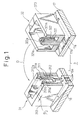
- Fig. 1 shows a first embodiment of a connector assembly, according to the present invention, as a high density connector assembly used for high speed transmission.
- the connector assembly 3 is suitably used for connection between two circuit boards arranged parallel to each other.
- the connector assembly 3 includes a jack connector 31 and a plug connector 32, which are mounted on circuit boards 16, 17, respectively.
- the jack connector 31 includes a plurality of jack-type pairs of signal contact elements 311, a plurality of jack-type ground contact elements 312 and a jack-type electro-insulating body 313.
- the plural pairs of signal contact elements 311 are arranged parallel with each other in an array. Each pair of signal contact elements 311 defines a jack contact pair and is used for a balanced transmission line.
- the plural ground contact elements 312 are also arranged parallel with each other in an array.
- the plural pairs of signal contact elements 311 and the plural ground contact elements 312 are alternately arranged in a single row. Each ground contact element 312 is used as a shield to reduce or suppress crosstalk between two pairs of signal contact elements arranged side by side in the row.
- the jack-type electro-insulating body 313 holds the jack-type pairs of signal contact elements 311 and the jack-type ground contact elements 312, as well as two opposed signal contact elements 311 of each pair, in a mutually insulated arrangement.
- the plug connector 32 includes a plurality of plug-type pairs of signal contact elements 321, a plurality of plug-type ground contact elements 322 and a plug-type electro-insulating body 323.
- the plural pairs of signal contact elements 321 are arranged parallel with each other in an array. Each pair of signal contact elements 321 defines a plug contact pair and is used for a balanced transmission line.
- the plural ground contact elements 322 are also arranged parallel with each other in an array.
- the plural pairs of signal contact elements 321 and the plural ground contact elements 322 are alternately arranged in a single row. Each ground contact element 322 is used as a shield to reduce or suppress crosstalk between two pairs of signal contact elements 321 arranged side by side in the row.
- the plug-type electro-insulating body 323 holds the plug-type pairs of signal contact elements 321 and the plug-type ground contact elements 322, as well as two opposed signal contact elements 321 of each pair, in a mutually insulated arrangement.
- Each signal contact element 311 (or a jack signal contact 311) of the jack connector 31 includes a contact end 311a used to be slidably engaged with a contact end 321a of each counterpart signal contact element 321 (or a plug signal contact 321) of the plug connector 32.
- each ground contact element 312 (or a jack ground contact 312) of the jack connector 31 includes a contact end 312a used to be slidably engaged with a contact end 322a of each ground contact element 322 (or a plug ground contact 322) of the plug connector 32.
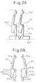
- Fig. 2A shows a blank 311' of the jack signal contact 311, prepared by a conventional press-stamping process
- Fig. 2B shows a detail of the jack signal contact 311 obtained from the blank 311'.
- a plurality of blanks 311' are joined together by a connecting part 311" into a comb shape.
- the jack signal contact 311 includes the contact end 311a formed along an edge of one end portion of the contact 311, which is curved convexly toward one lateral side of the contact 311, an intermediate, insulator engagement section 311b adjacent to the contact end 311a, and an external terminal 311c adjacent to the section 311b at the other end of the contact 311.
- a narrow extension having the contact end 311a extends from the engagement section 311b along one lateral edge of the section 311b, and another narrow extension having the external terminal 311c extends oppositely from the engagement section 311b along the other lateral edge of the section 311b.
- the external terminal 311c is joined to the connecting part 311", and thus the contact 311 is formed by cutting off the external terminal 311c from the connecting part 311".
- the engagement section 311b is provided at both lateral edges thereof with two pairs of bulges or projections 311b', which act to fasten the engagement section 311b to the jack-type electro-insulating body 313 (or a jack insulator 313).
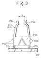
- Fig. 3 shows a blank 312' of the jack ground contact 312, prepared by a conventional press-stamping process.
- a plurality of blanks 312' are joined together by a connecting part 312" into a comb shape.
- the jack ground contact 312, obtained from the blank 312' includes a pair of contact ends 312a, each of which has a same shape and structure as the contact end 311a of the jack signal contact 311 and thus is curved convexly toward the opposed contact, an intermediate, insulator engagement section 312b adjacent to the contact ends 312a, which has a same size in a longitudinal direction of the contact as the insulator engagement section 311b of the jack signal contact 311, and a pair of external terminals 312c adjacent to the section 312b, each of which has a same shape as the external terminal 311c of the jack signal contact 311.
- Narrower extensions having the contact ends 312a extend from the engagement section 312b along both lateral edges of the section 312b, and narrower extensions having the external terminals 312c extend oppositely from the engagement section 312b along the both lateral edges of the section 312b.
- the external terminals 312c are joined to the connecting part 312", and thus the contact 312 is formed by cutting off the external terminals 312c from the connecting part 312".
- the engagement section 312b is provided at both lateral edges thereof with two pairs of bulges or projections 312b', which act to fasten the engagement section 312b to the jack insulator 313.
- a distance "g" between two contact ends 312a is selected to be equal to a distance between two contact ends 311a of one pair of opposed jack signal contacts 311 inserted into opposed slits 313d ( Fig. 4A ) formed in the jack insulator 313. Also, the length of each extension having the contact end 312a and the length of each external terminal 312c of the jack ground contact 312 are substantially equal, respectively, to the length of extension having the contact end 311a and the length of external terminal 311c of the jack signal contact 311.
- each of the ground contact elements 312 has a portion, a profile of which substantially corresponds to a profile of each pair of signal contact elements 311. Therefore, each ground contact element 312 can overlap two pairs of signal contact elements 311 arranged side by side in the row in the jack insulator 313, and thus acts as a shield to reduce or suppress crosstalk between the two pairs of signal contact elements 311.
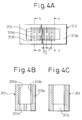
- Figs. 4A to 4C show the jack insulator 313 in a plan view, a b-b section and a c-c section, respectively.
- the jack insulator 313 is shaped as a bottomed box provided with a peripheral wall 313a having a height slightly larger than the length of each extension for the contact end 311a, 312a of the jack signal contact 311 and the jack ground contact 312.
- a plurality of grooves 313b extending from the open end to the inner surface of the bottom wall of the insulator 313, are formed in parallel to and oppositely aligned to each other in a pitch "p/2" i.e. half the pitch "p" of the plural pairs of the jack signal contact 311.
- a plurality of slits 313c, 313d are formed tb penetrate the bottom wall and to be aligned with the respective grooves 313b.
- Each slit 313c, 313d has a same thickness as the each groove 313b, and the thickness of each of the slits 313c, 313d and grooves 313b is slightly larger than the thickness of each of the jack signal and ground contacts 311, 312.
- Each of the larger slits 313c extends laterally between opposed grooves 313b and can fixedly receive the engagement section 312b of the jack ground contact 312, and each of the smaller slits 313d extends laterally from respective one of remaining grooves 313b to a midway of the bottom wall and can fixedly receive the engagement section 311b of the jack signal contact 311.
- the plural larger slits 313c and the plural pairs of opposed smaller slits 313d are alternately arranged in a row.
- the plural pairs of jack signal contacts 311 are inserted into the respective slits 313d, in such an arrangement that the contact ends 311a of each pair are opposed to each other, with the contact ends 311a being leading ends in a direction shown by an arrow E 1 , and the engagement sections 311b are press-fit in the slits 313d.
- the plural jack ground contacts 312 are inserted into the respective slits 313c with the contact ends 312a being leading ends in a direction shown by an arrow E 2 , and the engagement sections 312b are press-fit in the slits 313c.
- the contact ends 311a of the jack signal contacts 311 are aligned with each other in the longitudinal direction of the jack insulator 313.
- the contact ends 311a of the jack signal contacts 311 and the contact ends 312a of the jack ground contacts 312 are aligned with each other in the direction of the row of these contacts 311, 312 while maintaining the distance "g" between the opposed pair of contact ends 311a, 312a.
- the external terminals 311c of the jack signal contacts 311 and the external terminals 312c of the jack ground contacts 312 are arranged in a staggered manner in four separate rows of the terminals 311c, 312c.
- the circuit board 16 ( Fig. 1 ) is provided with a plurality of through holes 16a in an array corresponding to the staggered array of the terminals 311c, 312c. Accordingly, it is possible to mount the jack connector 31 on the surface of the circuit board 16 by inserting the terminals 311c, 312c into the respective through holes 16a. Then, the terminals 311c of the jack signal contacts 311 are fixedly connected with signal lines provided on the circuit board 16, and the terminals 312c of the jack ground contacts 312 are fixedly connected with a ground provided on the circuit board 16.
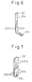
- Fig. 6 shows a detail of the plug signal contact 321, prepared by a conventional press-stamping and bending process.
- the plug signal contact 321 includes the contact end 321a formed on a flat surface of one end portion of the contact 321, an intermediate insulator engagement section 321b adjacent to the contact end 321a, and an external terminal 321c adjacent to the section 321b at the other end of the contact 321.
- An extension having the contact end 321a extends from the engagement section 321b parallel to the section 321b, and another extension having the external terminal 321c extends oppositely from the engagement section 321b orthogonally to the section 321b.
- the plug signal contact 321 has a constant lateral size throughout the entire length thereof, which is larger than the thickness of the jack signal contact 311. Also, the extension having the contact end 321a has a length shorter than the length of the extension having the contact end 311a of the jack signal contact 311.
- the engagement section 321b is provided at both lateral edges thereof with two bulges or projections 321b', which act to fasten the engagement section 321b to the plug-type electro-insulating body 323 (or a plug insulator 323).
- Fig. 7 shows a detail of the plug ground contact 322, prepared by a conventional press-stamping and bending process from a blank material thicker than that of the jack ground contact 312.
- the plug ground contact 322 includes a pair of contact ends 322a formed along opposed lateral edges of one end portion of the contact 322, an intermediate insulator engagement section 322b adjacent to the contact ends 322a, which has a same size in a longitudinal direction of the contact as the insulator engagement section 321b of the plug signal contact 321, and an external terminal 322c adjacent to the section 322b.
- An extension having the contact ends 322a extends from the engagement section 322b parallel to the section 322b, and the external terminal 322c is formed as a pad on the lower edge of the engagement section 322b.
- the engagement section 322b is provided at both lateral edges thereof with two pairs of bulges or projections 322b', which act to fasten the engagement section 322b to the plug insulator 323.
- a lateral distance between two contact ends 322a is selected to be equal to a distance between two contact ends 321a of one pair of opposed plug signal contacts 321 inserted into opposed slits 323d ( Fig. 8A ) formed in the plug insulator 323. Also, the length of the extension having the contact ends 322a is substantially equal to the length of extension having the contact end 321a of the plug signal contact 321.
- each ground contact element 322 can overlap two pairs of signal contact elements 321 arranged side by side in the row in the plug insulator 323, and thus acts as a shield to reduce or suppress crosstalk between the two pairs of signal contact elements 321.
- Figs. 8A to 8C show the plug insulator 323 in a plan view, a b-b section and a c-c section, respectively.
- the plug insulator 323 is shaped as a bottomed box provided with a peripheral wall 323a having a height slightly larger than the length of each extension for the contact end 321a, 322a of the plug signal contact 321 and the plug ground contact 322.
- the peripheral wall 323a has an inner surface capable of fitting with the outer surface of the peripheral wall 313a of the jack insulator 313.
- a plurality of slits 323b are formed to penetrate the bottom wall and to be aligned with the respective slits 313c of the jack insulator 313 when the plug insulator 323 is fitted with the jack insulator 313 under an interengagement between the peripheral-walls 323a and 313a.
- Each slit 323b extends laterally in a center region of the bottom wall of the plug insulator 323 and can fixedly receive the engagement section 322b of the plug ground contact 322.
- a plurality of partition walls 323c is formed to project from the bottom wall and to be aligned with the respective slits 313d of the jack insulator 313 when the plug insulator 323 is fitted with the jack insulator 313.
- Each partition wall 323c has a height slightly lower than that of the peripheral wall 323a and a lateral size slightly smaller than that of the slit 323b.
- slits 323d are formed to penetrate through the bottom wall.
- Each slit 323d can fixedly receive the engagement section 321b of the plug signal contact 321.
- the plural slits 323c and the plural pairs of opposed slits 323d are alternately arranged in a row.
- the plural pairs of plug signal contacts 321 are inserted into the respective slits 323d, in such an arrangement that the extensions having the contact ends 321a of each pair are abutted onto the opposed side faces of the partition wall 323c and the external terminals 321c of each pair extend away from each other, with the contact ends 321a being leading ends in a direction shown by arrows F 1 , and the engagement sections 321b are press-fit in the slits 323d.
- the plural plug ground contacts 322 are inserted into the respective slits 323b with the contact ends 322a being leading ends in a direction shown by an arrow F 2 , and the engagement sections 322b are press-fit in the slits 323b.
- the contact ends 321a of the plug signal contacts 321 are aligned with each other in the longitudinal direction of the plug insulator 323, and the contact ends 322a of the plug ground contacts 322 are located between and parallel to the partition wall 323c.
- the contact ends 321a of the plug signal contacts 321 and the contact ends 322a of the plug ground contacts 322 are aligned with each other in the direction of the row of these contacts 321, 322 while maintaining the distance between the opposed pair of contact ends 321a, 322a.
- the external terminals 321c of the plug signal contacts 321 and the external terminals 322c of the plug ground contacts 322 are arranged, in a staggered manner, in three separate rows of the terminals 321c, 322c.
- the circuit board 17 ( Fig. 1 ) is provided with a plurality of signal electrodes 17a and ground electrodes 17b in an array corresponding to the staggered array of the terminals 321c, 322c. Accordingly, it is possible to mount the plug connector 32 on the surface of the circuit board 17 by putting the terminals 321c, 322c onto the respective electrodes 17a, 17b. Then, the terminals 321c of the plug signal contacts 321 are fixedly connected with signal electrodes 17a provided on the circuit board 17, and the terminals 322c of the plug ground contacts 322 are fixedly connected with a ground electrodes 17b provided on the circuit board 17.
- the plug connector 32 When the plug connector 32 is suitably fitted with the jack connector 31 as shown by an arrow D in Fig. 1 , it is possible to provide the high-speed transmission connector assembly 3, wherein the plural pairs of plug signal contacts 321 of the plug connector 32 are connected with the corresponding, plural pairs of jack signal contacts 311 of the jack connector 31, to define plural pairs of signal transmission contact lines, and the plural plug ground contacts 322 of the plug connector 32 are connected with the plural jack ground contacts 312 of the jack connector 31, to define plural ground contact lines.
- each ground contact line, structured from the mutually connected jack and plug ground contacts 312, 322 is interposed as a shield between two pairs of signal transmission contact lines, structured from the mutually connected jack and plug signal contacts 311, 321, arranged side by side in the row of contacts, and thereby it is possible to reduce or suppress the crosstalk between the two pairs of signal transmission contact lines. Also, it is possible to eliminate the crosstalk between the laterally opposed signal transmission contact lines of each pair, by connecting these opposed signal transmission contact lines with a balanced transmission line, since the balanced transmission line causes a virtual ground plane between a pair of signal lines used therefor.
- Fig. 10 illustrates a second embodiment of a connector assembly, according to the present invention, as a high density connector assembly used for high speed transmission.
- the connector assembly 4 is suitably used for connection between two circuit boards arranged orthogonal to each other.
- the connector assembly 4 includes a jack connector 31 and a plug connector 42, which are mounted on circuit boards 16, 18, respectively.
- the jack connector 31 and the circuit board 16 have a structure identical to those in the first embodiment, and thus the description thereof is not repeated.
- the plug connector 42 includes a plurality of plug-type pairs of right-angled signal contact elements 421, a plurality of plug-type right-angled ground contact elements 422 and a plug-type electro-insulating body 423.
- the plural pairs of signal contact elements 421 are arranged parallel with each other in an array. Each pair of signal contact elements 421 defines a plug contact pair and is used for a balanced transmission line.
- the plural ground contact elements 422 are also arranged parallel with each other in an array.
- the plural pairs of signal contact elements 421 and the plural ground contact elements 422 are alternately arranged in a single row. Each ground contact element 422 is used as a shield to reduce or suppress crosstalk between two pairs of signal contact elements 421 arranged side by side in the row.
- the plug-type electro-insulating body 423 holds the plug-type pairs of signal contact elements 421 and the plug-type ground contact elements 422, as well as two opposed signal contact elements 421 of each pair, in a mutually insulated arrangement.
- Each signal contact element 421 (or a plug signal contact 421) includes a contact end 421a and an insulator engagement section 421b, both having the same structure of the contact end 321a and the insulator engagement section 321b, respectively, of the plug signal contact 321 of the first embodiment.
- each ground contact element 422 (or a plug ground contact 422) of the plug connector 42 includes contact ends 422a and an insulator engagement section 422b, both having the same structure of the contact ends 322a and the insulator engagement section 322b, respectively, of the plug ground contact 322 of the first embodiment. The description of these same or similar structures of the contacts 421, 422 are not repeated.
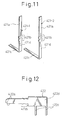
- Fig. 11 shows a detail of the right-angled plug signal contact 421, prepared by a conventional press-stamping and bending process.
- the right-angled plug signal contact 421 includes the contact end 421a, the insulator engagement section 421b, and an extension 421d adjacent to the section 421b and bent at a right angle to define an external terminal 421c at the other end of the contact 421.
- the contact end 421a extends parallel to the section 421b, and the external terminal 421c extends orthogonally to the section 421b.
- Each pair of plug signal contacts 421 includes a shorter one 421-1 having a shorter extension 421d and a longer one 421-2 having a longer extension 421d.
- the right-angled plug signal contact 421 has a constant lateral size throughout the entire length thereof, which is larger than the thickness of the jack signal contact 311. Also, the extension having the contact end 421a has a length shorter than the length of the extension having the contact end 311a of the jack signal contact 311.
- Fig. 12 shows a detail of the right-angled plug ground contact 422, prepared by a conventional press-stamping and bending process from a blank material thicker than that of the jack ground contact 312.
- the right-angled plug ground contact 422 includes the pair of contact ends 422a, the insulator engagement section 422b, and an extension 422d adjacent to the section 422b and having a pair of external terminals 422c extend at a right angle from one lateral side of the section 422b.
- the contact end 422a extends parallel to the section 422b, and the external terminals 422c extend orthogonally to the section 422b.
- a lateral distance between two contact ends 422a is selected to be equal to a distance between two contact ends 421a of one pair of opposed plug signal contacts 421 inserted into opposed slits 423d ( Fig. 13A ) formed in the plug-type electro-insulating body 423 (or a plug insulator 423). Also, the length of the extension having the contact ends 422a is substantially equal to the length of the extension having the contact end 421a of the plug signal contact 421.
- each ground contact element 422 can overlap two pairs of signal contact elements 421 arranged side by side in the row in the plug insulator 423, and thus acts as a shield to reduce or suppress crosstalk between the two pairs of signal contact elements 421.
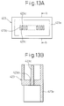
- Figs. 13A and 13B show the plug insulator 423 in a plan view and a b-b section, respectively.
- the plug insulator 423 has generally the same structure as the plug insulator 323 of the first embodiment, except that an extension wall 423e is added to the upper section identical to the plug insulator 323.
- the extension wall 423e extends from the bottom wall of the upper section along three edges of the bottom wall, and acts to cover the right-angled extensions 421d, 422d of the signal and ground contacts 421, 422 held in positions in the plug insulator 423.
- the description of the same or similar structures of the plug insulator 423 are not repeated.
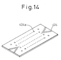
- the plug connector 42 further includes a locator 424 for positioning and holding the external terminals 421c, 422c of the right-angled plug signal and ground contacts 421, 422 at mutually spaced positions.
- the locator 424 is shaped as a flat rectangular plate and is mounted to the extension wall 423e of the plug insulator 423 along the remaining edge of the bottom wall of the insulator 423.
- the locator 424 is provided with a plurality of holes 424a at positions corresponding to the external terminals 421c, 422c of the right-angled plug signal and ground contacts 421, 422, both incorporated into the plug insulator 423.
- Each terminal hole 424a has a dimension allowing the external terminal 421c, 422c to be somewhat loosely inserted into the same.
- the plural pairs of right-angled plug signal contacts 421-1, 421-2 are inserted into the respective slits 423d of the plug insulator 423, in such an arrangement that the extensions having the contact ends 421a of each pair abut the opposed side faces of the partition wall 423c and the external terminals 421c of each pair are extend in the same direction, with the contact ends 421a being leading ends in a direction shown by arrows H 1 , H 2 , and the engagement sections 421b are press-fit in the slits 423d.
- the plural right-angled plug ground contacts 422 are inserted into the respective slits 423b with the contact ends 422a being leading ends in a direction shown by an arrow H 3 , and the engagement sections 422b are press-fit in the slits 423b.
- the contact ends 421a of the plug signal contacts 421 are aligned with each other in the longitudinal direction of the plug insulator 423, and the contact ends 422a of the plug ground contacts 422 are located between, and parallel to, the partition wall 423c.
- the contact ends 421a of the plug signal contacts 421 and the contact ends 422a of the plug ground contacts 422 are aligned with each other in the direction of the row of these contacts 421, 422 while maintaining a distance between the opposed pair of contact ends 421a, 422a.
- the external terminals 421c of the plug signal contacts 421 and the external terminals 422c of the plug ground contacts 422 are arranged in a staggered manner in four separate rows of the terminals 421c, 422c.
- the locator 424 is mounted to the plug insulator 423 as shown by an arrow H 4 at a position for enabling the holes 424a of the locator 424 to receive the right-angled terminals 421c, 422c.
- the plug connector 42 as shown in Fig. 10 , wherein the external terminals 421b of the plug signal contacts 421 and the external terminals 422b of the plug ground contact 422b are arranged and positioned in a staggered manner.
- the circuit board 18 ( Fig. 10 ) is provided with a plurality of through holes 18a in an array corresponding to the staggered array of the terminals 421c, 422c. Accordingly, it is possible to mount the plug connector 42 on the surface of the circuit board 18 by inserting the terminals 421c, 422c into the respective through holes 18a. Then, the terminals 421c of the plug signal contacts 421 are fixedly connected with signal lines provided on the circuit board 18, and the terminals 422c of the jack ground contacts 422 are fixedly connected with a ground provided on the circuit board 18.
- the plug connector 42 When the plug connector 42 is suitably fitted with the jack connector 31 as shown by an arrow G in Fig. 10 , it is possible to provide the high-speed transmission connector assembly 4, wherein the plural pairs of plug signal contacts 421 of the plug connector 42 are connected with the corresponding plural pairs of jack signal contacts 311 of the jack connector 31, to define plural pairs of signal transmission contact lines, and the plural plug ground contacts 422 of the plug connector 42 are connected with the plural jack ground contacts 312 of the jack connector 31 to define plural ground contact lines.
- each ground contact line structured from the mutually connected jack and plug ground contacts 312, 422 is interposed as a shield between two pairs of signal transmission contact lines, structured from the mutually connected jack and plug signal contacts 311, 421, arranged side by side in the row of contacts, and thereby it is possible to reduce or suppress the crosstalk between the two pairs of signal transmission contact lines. Also, it is possible to eliminate the crosstalk between the laterally opposed signal transmission contact lines of each pair, by connecting these opposed signal transmission contact lines with a balanced transmission line, since the balanced transmission line causes a virtual ground plane between the pair of signal lines used therefor.
- Fig. 16 illustrates a third embodiment of a connector assembly, according to the present invention, as a high density connector assembly used for high speed transmission.
- the connector assembly 5 is suitably used for connection between two circuit boards arranged parallel to each other.
- the connector assembly 5 includes a jack connector 51 and a plug connector 52, which are mounted on circuit boards 19, 20, respectively.
- the jack connector 51 and the circuit board 19 have a similar structure to those in the first embodiment, except that separate shielding plates are provided in the jack connector 51.
- the plug connector 52 and the circuit board 20 have a similar structure to those in the first embodiment, except that separate shielding plates are provided in the plug connector 52. The description of the similar portion is not repeated.
- the jack connector 51 of the third embodiment has a pair of first shield plates 514 attached to the respective lateral outer surfaces of the peripheral wall 313a of the jack insulator 313.
- the first shield plates 514 extend alongside the row of the contacts 311, 312 over the entire area of the lateral outer surfaces.
- the first shield plates 514 may be bonded to the outer surfaces of the jack insulator 313 by, e.g., an adhesive.
- Each shield plate 514 has a plurality of tongues 514b extending from an edge 514a thereof towards the circuit board 19 and a plurality of small projections 514c formed on an outer surface thereof.
- the circuit board 19 is provided with a plurality of through holes 19a in an array corresponding to the staggered array of the terminals 311c, 312c ( Figs. 5A, 5B ).
- the circuit board 19 is also provided with holes 19b connected to a ground voltage, at positions corresponding to the tongues 514b of the first shield plates 514. Accordingly, it is possible to mount the jack connector 51 on the surface of the circuit board 19 by inserting the terminals 311c, 312c into the respective through holes 19a, and also inserting the tongues 514b into the respective holes 19b.
- terminals 311c of the plug signal contacts 311 are fixedly connected with signal lines provided on the circuit board 19, and the terminals 312c of the jack ground contacts 312 as well as the tongues 514b of the first shield plates 514 are fixedly connected with a ground provided on the circuit board 19.
- the plug connector 52 of the third embodiment has a pair of second shield plates 524 attached onto the respective lateral inner surfaces of the peripheral wall 323a of the plug insulator 323.
- the second shield plates 524 extend alongside the row of the contacts 321, 322 over the entire area of the lateral inner surfaces.
- the second shield plates 524 may be bonded to the inner surfaces of the plug insulator 323 by, e.g., an adhesive.
- Each shield plate 524 has a plurality of tongues 524b extending from an edge 524a thereof and penetrating though the bottom wall of the plug insulator 323.
- the circuit board 20 is provided with a plurality of signal electrodes 20a and ground electrodes 20b in an array corresponding to the staggered array of the terminals 321c, 322c ( Fig. 9 ).
- the circuit board 20 is also provided with holes 20c, connected to aground voltage, at positions corresponding to the tongues 524b of the second shield plates 524. Accordingly, it is possible to mount the plug connector 52 on the surface of the circuit board 20 by putting the terminals 321c, 322c onto the respective electrodes 20a, 20b, and inserting the tongues 524b into the respective holes 20c.
- terminals 321c of the plug signal contacts 321 are fixedly connected with signal electrodes 20a provided on the circuit board 20
- the terminals 322c of the plug ground contacts 322 are fixedly connected with a ground electrodes 20b provided on the circuit board 20
- tongues 524b of the second shield plates 524 are fixedly connected with the holes 20c.
- the plug connector 52 When the plug connector 52 is suitably fitted with the jack connector 51 as shown by an arrow I in Fig. 16 , it is possible to provide the high-speed transmission connector assembly 5, wherein the plural pairs of plug signal contacts 321 of the plug connector 52 are connected with the corresponding, plural pairs of jack signal contacts 311 of the jack connector 51, to define plural pairs of signal transmission contact lines, and the plural plug ground contacts 322 of the plug connector 52 are connected with the plural jack ground contacts 312 of the jack connector 51, to define plural ground contact lines. Also, in this embodiment, when the plug connector 52 is suitably fitted with the jack connector 51, the first shield plates 514 are connected with the second shield plates 524 through the projections 514c to define a frame ground surrounding the row of the contact lines.
- each ground contact line structured from the mutually connected jack and plug ground contacts 312, 322 is interposed as a shield between two pairs of signal transmission contact lines, structured from the mutually connected jack and plug signal contacts 311, 321, arranged side by side in the row of contacts, and thereby it is possible to reduce or suppress the crosstalk between the two pairs of signal transmission contact lines. Also, it is possible to eliminate the crosstalk between the laterally opposed signal transmission contact lines of each pair, by connecting these opposed signal transmission contact lines with a balanced transmission line, since the balanced transmission line causes a virtual ground plane between the pair of signal lines used therefor.
- the frame ground structured from the first and second shield plates 514, 524.
- the ground contact line structured from the mutually connected jack and plug ground contacts 312, 322, is disposed at respective one of opposed outermost positions in the row of the contact lines.
- Such shield plates used for the frame ground may also be incorporated into the connector assembly 4 of the second embodiment. In this case, it is apparent that the same effect as in the connector assembly 5 may be obtained.
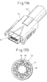
- Fig. 17A shows another embodiment of a connector, according to the present invention, as a high density connector used for high speed transmission.
- the connector 62 of this embodiment is suitably used for connection of a balanced transmission cable 63.
- the structure and function of the connector 62 are similar to those of the plug connectors of the above embodiments, and are not described in detail.
- the connector 62 may be fixed to the cable 63 by a resinous mold 64.
- the balanced transmission cable 63 includes plural balanced transmission lines 65, plural grounds 66 respectively surrounding each balanced transmission line (or a line pair) 65, a shield 67 enclosing all the balanced transmission lines 65 and grounds 66, and a sheath 68 surrounding the shield 67.
- the signal contact elements of the connector 62 are fixedly connected with the respective balanced transmission lines 65, and the ground contact elements of the connector 62 are fixedly connected with the respective grounds 66.
- the signal contact elements are arranged in two rows.
- the present invention should not be limited thereto, but may be applied to any other connectors having an even number of rows of signal contact elements.
Abstract
A connector assembly (3) includes a jack connector (31) and a plug connector (32). Each of the jack and plug connectors (31, 32) includes plural pairs of signal contact elements (311, 321), the pairs being arranged parallel with each other in an array, and the signal contact elements (311, 321) of each of the pairs being arranged opposite to each other; plural ground contact elements (312, 322), each of which is used as a shield to reduce crosstalk between two parallel the pairs of signal contact elements (311, 321) arranged side-by-side. The plural pairs of signal contact elements (311, 321) and the plural ground contact elements (312, 322) being alternately arranged in a row. An electro-insulating body supports the signal contact elements (311, 321) and the ground contact elements (312, 322) in mutually insulated arrangement. It is advantageous that each pair of signal contact elements (311, 321) is used for a balanced transmission line.
Description
- The present invention relates generally to an electrical connecting device and, more particularly, to a connector used for high speed transmission lines. The present invention further relates to a connector assembly including such a connector. The present invention is effective when used for connecting balanced transmission lines.
- Various types of connector systems used for connecting high speed transmission lines are well known in the art. One example of conventional connector systems for high speed transmission includes jack and plug connectors, each of which includes a plurality of signal contacts arranged in several rows in an electro-insulating body. In this type of conventional connector system or assembly, the signal lines structured by the mutually engaged contacts of the mutually assembled jack and plug connectors are partially shielded through the ground potential lines located between the rows of the signal contacts. To this end, each of the jack and plug connectors further includes a row of plural ground contacts arranged between the rows of signal contacts, which act as a shielding to reduce a crosstalk between the rows of signal contacts.
- The above conventional connector assembly is effectively.used for a single-ended transmission.
However, this connector assembly cannot reduce a crosstalk between the signal lines arranged side by side in each row of contacts. Therefore, it is difficult to use this connector assembly for significantly high speed transmission, such as 1 gigabit/sec or more. Also, this structure of connector assembly makes it difficult to reduce a dimension of the insulator body and to increase the density of the signal lines. -
JP-A-06243936 - Recently, a balanced data transmission system using balanced signals, that is, a differential data transmission system, has been developed for a high speed transmission, and it has been desired to provide a new connector system which can be effectively used for such a balanced data transmission.
- According to the invention we provided plug connector in accordance with claim 1 of the appended claims.
- It is advantageous that the profile of a portion of each of the ground contact elements substantially corresponds to a profile of the each pair of signal contact elements.
- It is preferred that at least one of the ground contact elements is disposed at at least one of opposed outermost positions in the row.
- It is also advantageous that the connector further comprises at least one shield plate disposed outside of the row to reduce crosstalk between the pairs of signal contact elements and the exterior of the connector.
- For the jack connector, each pair of signal contact elements may define a jack-type contact pair, and each of the ground contact elements may define a jack contact.
- For the plug connector, each pair of signal contact elements may define a plug-type contact pair, and each of the ground contact elements may define a plug contact.
- It is advantageous that the each jack-type pair of signal contact elements and each plug-type pair of signal contact elements are used for a balanced transmission line.
- Particular embodiments of connectors in accordance with this invention will now be described with reference to the accompanying drawings, in which:-
-
Fig. 1 is a partial cross sectioned, perspective view of a connector assembly, in a separated state, according to a first embodiment of the present invention; -
Fig. 2A and 2B show a signal contact element of the jack connector of the connector assembly ofFig. 1 ; -
Fig. 3 shows a ground contact element of the jack connector of the connector assembly ofFig. 1 ; -
Fig. 4A is a plan view of an electro-insulating body of the jack connector ofFig. 1 ; -
Fig. 4B is a sectional view taken along line b-b ofFig. 4A ; -
Fig. 4C is a sectional view taken along line c-c ofFig. 4A ; -
Fig. 5A is a sectional view for illustrating the assembling process of the jack connector ofFig. 1 ; -
Fig. 5B is a sectional view for illustrating the - assembling process of the jack connector of
Fig. 1 ; -
Fig. 6 is a perspective view of a signal contact element of the plug connector of the connector assembly ofFig. 1 ; -
Fig. 7 is a perspective view of a ground contact element of the jack connector of the connector assembly ofFig. 1 ; -
Fig. 8A is a plan view of an electro-insulating body of the jack connector ofFig. 1 ; -
Fig. 8B is a sectional view taken along line b-b ofFig. 8A ; -
Fig. 8C is a sectional view taken along line c-c ofFig. 8A ; -
Fig. 9 is a sectional view for illustrating the assembling process of the plug connector ofFig. 1 ; -
Fig. 10 is a sectional view of a connector assembly, in a separated state, according to a second embodiment of the present invention; -
Fig. 11 shows two types of signal contact elements of the plug connector of Lhe connector assembly ofFig. 10 ; -
Fig. 12 shows a ground contact element of the plug connector of the connector assembly ofFig. 10 ; -
Fig. 13A is a plan view of an electro-insulating body of the plug connector ofFig. 10 ; -
Fig. 13B is a sectional view taken along line b-b ofFig. 13A ; -
Fig. 14 is a perspective view of a locator of the plug connector ofFig. 10 ; -
Fig. 15 is a sectional view for illustrating the assembling process of the plug connector ofFig. 10 ; -
Fig. 16 is a sectional view of a connector assembly, in a separated state, according to a third embodiment of the present invention; -
Fig. 17A is a perspective view of a connector, according to another embodiment of the present invention; andFig. 17B is a sectional view of a cable. - Referring to the drawings,
Fig. 1 shows a first embodiment of a connector assembly, according to the present invention, as a high density connector assembly used for high speed transmission. Theconnector assembly 3 is suitably used for connection between two circuit boards arranged parallel to each other. Theconnector assembly 3 includes ajack connector 31 and aplug connector 32, which are mounted oncircuit boards - The
jack connector 31 includes a plurality of jack-type pairs ofsignal contact elements 311, a plurality of jack-typeground contact elements 312 and a jack-type electro-insulatingbody 313. The plural pairs ofsignal contact elements 311 are arranged parallel with each other in an array. Each pair ofsignal contact elements 311 defines a jack contact pair and is used for a balanced transmission line. The pluralground contact elements 312 are also arranged parallel with each other in an array. The plural pairs ofsignal contact elements 311 and the pluralground contact elements 312 are alternately arranged in a single row. Eachground contact element 312 is used as a shield to reduce or suppress crosstalk between two pairs of signal contact elements arranged side by side in the row. The jack-type electro-insulatingbody 313 holds the jack-type pairs ofsignal contact elements 311 and the jack-typeground contact elements 312, as well as two opposedsignal contact elements 311 of each pair, in a mutually insulated arrangement. - The
plug connector 32 includes a plurality of plug-type pairs ofsignal contact elements 321, a plurality of plug-typeground contact elements 322 and a plug-type electro-insulatingbody 323. The plural pairs ofsignal contact elements 321 are arranged parallel with each other in an array. Each pair ofsignal contact elements 321 defines a plug contact pair and is used for a balanced transmission line. The pluralground contact elements 322 are also arranged parallel with each other in an array. The plural pairs ofsignal contact elements 321 and the pluralground contact elements 322 are alternately arranged in a single row. Eachground contact element 322 is used as a shield to reduce or suppress crosstalk between two pairs ofsignal contact elements 321 arranged side by side in the row. The plug-type electro-insulatingbody 323 holds the plug-type pairs ofsignal contact elements 321 and the plug-typeground contact elements 322, as well as two opposedsignal contact elements 321 of each pair, in a mutually insulated arrangement. - Each signal contact element 311 (or a jack signal contact 311) of the
jack connector 31 includes acontact end 311a used to be slidably engaged with acontact end 321a of each counterpart signal contact element 321 (or a plug signal contact 321) of theplug connector 32. Also, each ground contact element 312 (or a jack ground contact 312) of thejack connector 31 includes acontact end 312a used to be slidably engaged with acontact end 322a of each ground contact element 322 (or a plug ground contact 322) of theplug connector 32. -
Fig. 2A shows a blank 311' of thejack signal contact 311, prepared by a conventional press-stamping process, andFig. 2B shows a detail of thejack signal contact 311 obtained from the blank 311'. A plurality of blanks 311' are joined together by a connectingpart 311" into a comb shape. Thejack signal contact 311 includes thecontact end 311a formed along an edge of one end portion of thecontact 311, which is curved convexly toward one lateral side of thecontact 311, an intermediate,insulator engagement section 311b adjacent to thecontact end 311a, and anexternal terminal 311c adjacent to thesection 311b at the other end of thecontact 311. A narrow extension having thecontact end 311a extends from theengagement section 311b along one lateral edge of thesection 311b, and another narrow extension having theexternal terminal 311c extends oppositely from theengagement section 311b along the other lateral edge of thesection 311b. - In the blank 311', the
external terminal 311c is joined to the connectingpart 311", and thus thecontact 311 is formed by cutting off theexternal terminal 311c from the connectingpart 311". Theengagement section 311b is provided at both lateral edges thereof with two pairs of bulges orprojections 311b', which act to fasten theengagement section 311b to the jack-type electro-insulating body 313 (or a jack insulator 313). -
Fig. 3 shows a blank 312' of thejack ground contact 312, prepared by a conventional press-stamping process. A plurality of blanks 312' are joined together by a connectingpart 312" into a comb shape. Thejack ground contact 312, obtained from the blank 312', includes a pair of contact ends 312a, each of which has a same shape and structure as thecontact end 311a of thejack signal contact 311 and thus is curved convexly toward the opposed contact, an intermediate,insulator engagement section 312b adjacent to the contact ends 312a, which has a same size in a longitudinal direction of the contact as theinsulator engagement section 311b of thejack signal contact 311, and a pair ofexternal terminals 312c adjacent to thesection 312b, each of which has a same shape as theexternal terminal 311c of thejack signal contact 311. Narrower extensions having the contact ends 312a extend from theengagement section 312b along both lateral edges of thesection 312b, and narrower extensions having theexternal terminals 312c extend oppositely from theengagement section 312b along the both lateral edges of thesection 312b. - In the blank 312', the
external terminals 312c are joined to the connectingpart 312", and thus thecontact 312 is formed by cutting off theexternal terminals 312c from the connectingpart 312". Theengagement section 312b is provided at both lateral edges thereof with two pairs of bulges orprojections 312b', which act to fasten theengagement section 312b to thejack insulator 313. - A distance "g" between two contact ends 312a is selected to be equal to a distance between two contact ends 311a of one pair of opposed
jack signal contacts 311 inserted into opposedslits 313d (Fig. 4A ) formed in thejack insulator 313. Also, the length of each extension having thecontact end 312a and the length of eachexternal terminal 312c of thejack ground contact 312 are substantially equal, respectively, to the length of extension having thecontact end 311a and the length of external terminal 311c of thejack signal contact 311. - That is, in the
jack connector 31, each of theground contact elements 312 has a portion, a profile of which substantially corresponds to a profile of each pair ofsignal contact elements 311. Therefore, eachground contact element 312 can overlap two pairs ofsignal contact elements 311 arranged side by side in the row in thejack insulator 313, and thus acts as a shield to reduce or suppress crosstalk between the two pairs ofsignal contact elements 311. -
Figs. 4A to 4C show thejack insulator 313 in a plan view, a b-b section and a c-c section, respectively. Thejack insulator 313 is shaped as a bottomed box provided with aperipheral wall 313a having a height slightly larger than the length of each extension for thecontact end jack signal contact 311 and thejack ground contact 312. On the longitudinal, inner opposed surfaces of theperipheral wall 313a, a plurality ofgrooves 313b, extending from the open end to the inner surface of the bottom wall of theinsulator 313, are formed in parallel to and oppositely aligned to each other in a pitch "p/2" i.e. half the pitch "p" of the plural pairs of thejack signal contact 311. - In the bottom wall of the
insulator 313, a plurality ofslits respective grooves 313b. Eachslit groove 313b, and the thickness of each of theslits grooves 313b is slightly larger than the thickness of each of the jack signal andground contacts larger slits 313c extends laterally betweenopposed grooves 313b and can fixedly receive theengagement section 312b of thejack ground contact 312, and each of thesmaller slits 313d extends laterally from respective one of remaininggrooves 313b to a midway of the bottom wall and can fixedly receive theengagement section 311b of thejack signal contact 311. The plurallarger slits 313c and the plural pairs of opposedsmaller slits 313d are alternately arranged in a row. - As shown in
Figs. 5A and 5B , the plural pairs ofjack signal contacts 311 are inserted into therespective slits 313d, in such an arrangement that the contact ends 311a of each pair are opposed to each other, with the contact ends 311a being leading ends in a direction shown by an arrow E1, and theengagement sections 311b are press-fit in theslits 313d. Also, the pluraljack ground contacts 312 are inserted into therespective slits 313c with the contact ends 312a being leading ends in a direction shown by an arrow E2, and theengagement sections 312b are press-fit in theslits 313c. - When the
jack ground contacts 312 are fastened into therespective slits 313c and thejack signal contacts 311 are fastened into therespective slits 313d, the contact ends 311a of thejack signal contacts 311 are aligned with each other in the longitudinal direction of thejack insulator 313. - In the
jack connector 31 of the first embodiment assembled in this manner, the contact ends 311a of thejack signal contacts 311 and the contact ends 312a of thejack ground contacts 312 are aligned with each other in the direction of the row of thesecontacts external terminals 311c of thejack signal contacts 311 and theexternal terminals 312c of thejack ground contacts 312 are arranged in a staggered manner in four separate rows of theterminals - The circuit board 16 (
Fig. 1 ) is provided with a plurality of throughholes 16a in an array corresponding to the staggered array of theterminals jack connector 31 on the surface of thecircuit board 16 by inserting theterminals holes 16a. Then, theterminals 311c of thejack signal contacts 311 are fixedly connected with signal lines provided on thecircuit board 16, and theterminals 312c of thejack ground contacts 312 are fixedly connected with a ground provided on thecircuit board 16. -
Fig. 6 shows a detail of theplug signal contact 321, prepared by a conventional press-stamping and bending process. Theplug signal contact 321 includes thecontact end 321a formed on a flat surface of one end portion of thecontact 321, an intermediateinsulator engagement section 321b adjacent to thecontact end 321a, and anexternal terminal 321c adjacent to thesection 321b at the other end of thecontact 321. An extension having thecontact end 321a extends from theengagement section 321b parallel to thesection 321b, and another extension having theexternal terminal 321c extends oppositely from theengagement section 321b orthogonally to thesection 321b. - The
plug signal contact 321 has a constant lateral size throughout the entire length thereof, which is larger than the thickness of thejack signal contact 311. Also, the extension having thecontact end 321a has a length shorter than the length of the extension having thecontact end 311a of thejack signal contact 311. Theengagement section 321b is provided at both lateral edges thereof with two bulges orprojections 321b', which act to fasten theengagement section 321b to the plug-type electro-insulating body 323 (or a plug insulator 323). -
Fig. 7 shows a detail of theplug ground contact 322, prepared by a conventional press-stamping and bending process from a blank material thicker than that of thejack ground contact 312. Theplug ground contact 322 includes a pair of contact ends 322a formed along opposed lateral edges of one end portion of thecontact 322, an intermediateinsulator engagement section 322b adjacent to the contact ends 322a, which has a same size in a longitudinal direction of the contact as theinsulator engagement section 321b of theplug signal contact 321, and anexternal terminal 322c adjacent to thesection 322b. An extension having the contact ends 322a extends from theengagement section 322b parallel to thesection 322b, and theexternal terminal 322c is formed as a pad on the lower edge of theengagement section 322b. Theengagement section 322b is provided at both lateral edges thereof with two pairs of bulges orprojections 322b', which act to fasten theengagement section 322b to theplug insulator 323. - A lateral distance between two contact ends 322a is selected to be equal to a distance between two contact ends 321a of one pair of opposed
plug signal contacts 321 inserted into opposedslits 323d (Fig. 8A ) formed in theplug insulator 323. Also, the length of the extension having the contact ends 322a is substantially equal to the length of extension having thecontact end 321a of theplug signal contact 321. - That is, in the
plug connector 32, a portion of a profile of each of theground contact elements 322 substantially corresponds to a profile of each pair ofsignal contact elements 321. Therefore, eachground contact element 322 can overlap two pairs ofsignal contact elements 321 arranged side by side in the row in theplug insulator 323, and thus acts as a shield to reduce or suppress crosstalk between the two pairs ofsignal contact elements 321. -
Figs. 8A to 8C show theplug insulator 323 in a plan view, a b-b section and a c-c section, respectively. Theplug insulator 323 is shaped as a bottomed box provided with aperipheral wall 323a having a height slightly larger than the length of each extension for thecontact end plug signal contact 321 and theplug ground contact 322. Theperipheral wall 323a has an inner surface capable of fitting with the outer surface of theperipheral wall 313a of thejack insulator 313. - In the bottom wall of the
plug insulator 323, a plurality ofslits 323b are formed to penetrate the bottom wall and to be aligned with therespective slits 313c of thejack insulator 313 when theplug insulator 323 is fitted with thejack insulator 313 under an interengagement between the peripheral-walls slit 323b extends laterally in a center region of the bottom wall of theplug insulator 323 and can fixedly receive theengagement section 322b of theplug ground contact 322. - Also, in the center region of the bottom wall of the
plug insulator 323, a plurality ofpartition walls 323c is formed to project from the bottom wall and to be aligned with therespective slits 313d of thejack insulator 313 when theplug insulator 323 is fitted with thejack insulator 313. Eachpartition wall 323c has a height slightly lower than that of theperipheral wall 323a and a lateral size slightly smaller than that of theslit 323b. On both lateral sides of eachpartition wall 323c,slits 323d are formed to penetrate through the bottom wall. Eachslit 323d can fixedly receive theengagement section 321b of theplug signal contact 321. The plural slits 323c and the plural pairs ofopposed slits 323d are alternately arranged in a row. - As shown in
Fig. 9 , the plural pairs ofplug signal contacts 321 are inserted into therespective slits 323d, in such an arrangement that the extensions having the contact ends 321a of each pair are abutted onto the opposed side faces of thepartition wall 323c and theexternal terminals 321c of each pair extend away from each other, with the contact ends 321a being leading ends in a direction shown by arrows F1, and theengagement sections 321b are press-fit in theslits 323d. Also, the pluralplug ground contacts 322 are inserted into therespective slits 323b with the contact ends 322a being leading ends in a direction shown by an arrow F2, and theengagement sections 322b are press-fit in theslits 323b. - When the
plug ground contacts 322 are fastened into therespective slits 323c and theplug signal contacts 321 are fastened into therespective slits 323d, the contact ends 321a of theplug signal contacts 321 are aligned with each other in the longitudinal direction of theplug insulator 323, and the contact ends 322a of theplug ground contacts 322 are located between and parallel to thepartition wall 323c. In theplug connector 32 of the first embodiment assembled in this manner, the contact ends 321a of theplug signal contacts 321 and the contact ends 322a of theplug ground contacts 322 are aligned with each other in the direction of the row of thesecontacts external terminals 321c of theplug signal contacts 321 and theexternal terminals 322c of theplug ground contacts 322 are arranged, in a staggered manner, in three separate rows of theterminals - The circuit board 17 (
Fig. 1 ) is provided with a plurality of signal electrodes 17a andground electrodes 17b in an array corresponding to the staggered array of theterminals plug connector 32 on the surface of thecircuit board 17 by putting theterminals respective electrodes 17a, 17b. Then, theterminals 321c of theplug signal contacts 321 are fixedly connected with signal electrodes 17a provided on thecircuit board 17, and theterminals 322c of theplug ground contacts 322 are fixedly connected with aground electrodes 17b provided on thecircuit board 17. - When the
plug connector 32 is suitably fitted with thejack connector 31 as shown by an arrow D inFig. 1 , it is possible to provide the high-speedtransmission connector assembly 3, wherein the plural pairs ofplug signal contacts 321 of theplug connector 32 are connected with the corresponding, plural pairs ofjack signal contacts 311 of thejack connector 31, to define plural pairs of signal transmission contact lines, and the pluralplug ground contacts 322 of theplug connector 32 are connected with the pluraljack ground contacts 312 of thejack connector 31, to define plural ground contact lines. - In such a high-speed
transmission connector assembly 3, each ground contact line, structured from the mutually connected jack and plugground contacts signal contacts -
Fig. 10 illustrates a second embodiment of a connector assembly, according to the present invention, as a high density connector assembly used for high speed transmission. Theconnector assembly 4 is suitably used for connection between two circuit boards arranged orthogonal to each other. Theconnector assembly 4 includes ajack connector 31 and aplug connector 42, which are mounted oncircuit boards - In this embodiment, the
jack connector 31 and thecircuit board 16 have a structure identical to those in the first embodiment, and thus the description thereof is not repeated. - The
plug connector 42 includes a plurality of plug-type pairs of right-angledsignal contact elements 421, a plurality of plug-type right-angledground contact elements 422 and a plug-type electro-insulatingbody 423. The plural pairs ofsignal contact elements 421 are arranged parallel with each other in an array. Each pair ofsignal contact elements 421 defines a plug contact pair and is used for a balanced transmission line. The pluralground contact elements 422 are also arranged parallel with each other in an array. The plural pairs ofsignal contact elements 421 and the pluralground contact elements 422 are alternately arranged in a single row. Eachground contact element 422 is used as a shield to reduce or suppress crosstalk between two pairs ofsignal contact elements 421 arranged side by side in the row. The plug-type electro-insulatingbody 423 holds the plug-type pairs ofsignal contact elements 421 and the plug-typeground contact elements 422, as well as two opposedsignal contact elements 421 of each pair, in a mutually insulated arrangement. - Each signal contact element 421 (or a plug signal contact 421) includes a
contact end 421a and aninsulator engagement section 421b, both having the same structure of thecontact end 321a and theinsulator engagement section 321b, respectively, of theplug signal contact 321 of the first embodiment. Also, each ground contact element 422 (or a plug ground contact 422) of theplug connector 42 includes contact ends 422a and aninsulator engagement section 422b, both having the same structure of the contact ends 322a and theinsulator engagement section 322b, respectively, of theplug ground contact 322 of the first embodiment. The description of these same or similar structures of thecontacts -
Fig. 11 shows a detail of the right-angledplug signal contact 421, prepared by a conventional press-stamping and bending process. The right-angledplug signal contact 421 includes thecontact end 421a, theinsulator engagement section 421b, and anextension 421d adjacent to thesection 421b and bent at a right angle to define anexternal terminal 421c at the other end of thecontact 421. Thecontact end 421a extends parallel to thesection 421b, and theexternal terminal 421c extends orthogonally to thesection 421b. Each pair ofplug signal contacts 421 includes a shorter one 421-1 having ashorter extension 421d and a longer one 421-2 having alonger extension 421d. - The right-angled
plug signal contact 421 has a constant lateral size throughout the entire length thereof, which is larger than the thickness of thejack signal contact 311. Also, the extension having thecontact end 421a has a length shorter than the length of the extension having thecontact end 311a of thejack signal contact 311. -
Fig. 12 shows a detail of the right-angledplug ground contact 422, prepared by a conventional press-stamping and bending process from a blank material thicker than that of thejack ground contact 312. The right-angledplug ground contact 422 includes the pair of contact ends 422a, theinsulator engagement section 422b, and anextension 422d adjacent to thesection 422b and having a pair ofexternal terminals 422c extend at a right angle from one lateral side of thesection 422b. Thecontact end 422a extends parallel to thesection 422b, and theexternal terminals 422c extend orthogonally to thesection 422b. - A lateral distance between two contact ends 422a is selected to be equal to a distance between two contact ends 421a of one pair of opposed
plug signal contacts 421 inserted into opposedslits 423d (Fig. 13A ) formed in the plug-type electro-insulating body 423 (or a plug insulator 423). Also, the length of the extension having the contact ends 422a is substantially equal to the length of the extension having thecontact end 421a of theplug signal contact 421. - That is, in the
plug connector 42, a portion of the profile of each of theground contact elements 422 substantially corresponds to a profile of each pair ofsignal contact elements 421. Therefore, eachground contact element 422 can overlap two pairs ofsignal contact elements 421 arranged side by side in the row in theplug insulator 423, and thus acts as a shield to reduce or suppress crosstalk between the two pairs ofsignal contact elements 421. -
Figs. 13A and 13B show theplug insulator 423 in a plan view and a b-b section, respectively. Theplug insulator 423 has generally the same structure as theplug insulator 323 of the first embodiment, except that anextension wall 423e is added to the upper section identical to theplug insulator 323. Theextension wall 423e extends from the bottom wall of the upper section along three edges of the bottom wall, and acts to cover the right-angledextensions ground contacts plug insulator 423. The description of the same or similar structures of theplug insulator 423 are not repeated. - The
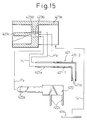
plug connector 42 further includes alocator 424 for positioning and holding theexternal terminals ground contacts Fig. 14 , thelocator 424 is shaped as a flat rectangular plate and is mounted to theextension wall 423e of theplug insulator 423 along the remaining edge of the bottom wall of theinsulator 423. Thelocator 424 is provided with a plurality ofholes 424a at positions corresponding to theexternal terminals ground contacts plug insulator 423. Eachterminal hole 424a has a dimension allowing theexternal terminal - As shown in
Fig. 15 , the plural pairs of right-angled plug signal contacts 421-1, 421-2 are inserted into therespective slits 423d of theplug insulator 423, in such an arrangement that the extensions having the contact ends 421a of each pair abut the opposed side faces of thepartition wall 423c and theexternal terminals 421c of each pair are extend in the same direction, with the contact ends 421a being leading ends in a direction shown by arrows H1, H2, and theengagement sections 421b are press-fit in theslits 423d. Also, the plural right-angledplug ground contacts 422 are inserted into therespective slits 423b with the contact ends 422a being leading ends in a direction shown by an arrow H3, and theengagement sections 422b are press-fit in theslits 423b. - When the
plug ground contacts 422 are fastened into therespective slits 423c and the plug signal contacts 421-1, 421-2 are fastened into therespective slits 423d, the contact ends 421a of theplug signal contacts 421 are aligned with each other in the longitudinal direction of theplug insulator 423, and the contact ends 422a of theplug ground contacts 422 are located between, and parallel to, thepartition wall 423c. In theplug connector 42 of the second embodiment assembled in this manner, the contact ends 421a of theplug signal contacts 421 and the contact ends 422a of theplug ground contacts 422 are aligned with each other in the direction of the row of thesecontacts external terminals 421c of theplug signal contacts 421 and theexternal terminals 422c of theplug ground contacts 422 are arranged in a staggered manner in four separate rows of theterminals - Then, the
locator 424 is mounted to theplug insulator 423 as shown by an arrow H4 at a position for enabling theholes 424a of thelocator 424 to receive the right-angledterminals plug connector 42 as shown inFig. 10 , wherein theexternal terminals 421b of theplug signal contacts 421 and theexternal terminals 422b of theplug ground contact 422b are arranged and positioned in a staggered manner. - The circuit board 18 (
Fig. 10 ) is provided with a plurality of throughholes 18a in an array corresponding to the staggered array of theterminals plug connector 42 on the surface of thecircuit board 18 by inserting theterminals holes 18a. Then, theterminals 421c of theplug signal contacts 421 are fixedly connected with signal lines provided on thecircuit board 18, and theterminals 422c of thejack ground contacts 422 are fixedly connected with a ground provided on thecircuit board 18. - When the
plug connector 42 is suitably fitted with thejack connector 31 as shown by an arrow G inFig. 10 , it is possible to provide the high-speedtransmission connector assembly 4, wherein the plural pairs ofplug signal contacts 421 of theplug connector 42 are connected with the corresponding plural pairs ofjack signal contacts 311 of thejack connector 31, to define plural pairs of signal transmission contact lines, and the pluralplug ground contacts 422 of theplug connector 42 are connected with the pluraljack ground contacts 312 of thejack connector 31 to define plural ground contact lines. - In such a high-speed
transmission connector assembly 4, each ground contact line, structured from the mutually connected jack and plugground contacts signal contacts -
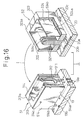
Fig. 16 illustrates a third embodiment of a connector assembly, according to the present invention, as a high density connector assembly used for high speed transmission. Theconnector assembly 5 is suitably used for connection between two circuit boards arranged parallel to each other. Theconnector assembly 5 includes ajack connector 51 and aplug connector 52, which are mounted oncircuit boards - In this embodiment, the
jack connector 51 and thecircuit board 19 have a similar structure to those in the first embodiment, except that separate shielding plates are provided in thejack connector 51. Also, theplug connector 52 and thecircuit board 20 have a similar structure to those in the first embodiment, except that separate shielding plates are provided in theplug connector 52. The description of the similar portion is not repeated. - The
jack connector 51 of the third embodiment has a pair offirst shield plates 514 attached to the respective lateral outer surfaces of theperipheral wall 313a of thejack insulator 313. Thefirst shield plates 514 extend alongside the row of thecontacts first shield plates 514 may be bonded to the outer surfaces of thejack insulator 313 by, e.g., an adhesive. Eachshield plate 514 has a plurality oftongues 514b extending from anedge 514a thereof towards thecircuit board 19 and a plurality ofsmall projections 514c formed on an outer surface thereof. - The
circuit board 19 is provided with a plurality of throughholes 19a in an array corresponding to the staggered array of theterminals Figs. 5A, 5B ). Thecircuit board 19 is also provided with holes 19b connected to a ground voltage, at positions corresponding to thetongues 514b of thefirst shield plates 514. Accordingly, it is possible to mount thejack connector 51 on the surface of thecircuit board 19 by inserting theterminals holes 19a, and also inserting thetongues 514b into the respective holes 19b. Then, theterminals 311c of theplug signal contacts 311 are fixedly connected with signal lines provided on thecircuit board 19, and theterminals 312c of thejack ground contacts 312 as well as thetongues 514b of thefirst shield plates 514 are fixedly connected with a ground provided on thecircuit board 19. - The
plug connector 52 of the third embodiment has a pair ofsecond shield plates 524 attached onto the respective lateral inner surfaces of theperipheral wall 323a of theplug insulator 323. Thesecond shield plates 524 extend alongside the row of thecontacts second shield plates 524 may be bonded to the inner surfaces of theplug insulator 323 by, e.g., an adhesive. Eachshield plate 524 has a plurality of tongues 524b extending from anedge 524a thereof and penetrating though the bottom wall of theplug insulator 323. - The
circuit board 20 is provided with a plurality ofsignal electrodes 20a andground electrodes 20b in an array corresponding to the staggered array of theterminals Fig. 9 ). Thecircuit board 20 is also provided withholes 20c, connected to aground voltage, at positions corresponding to the tongues 524b of thesecond shield plates 524. Accordingly, it is possible to mount theplug connector 52 on the surface of thecircuit board 20 by putting theterminals respective electrodes respective holes 20c. Then, theterminals 321c of theplug signal contacts 321 are fixedly connected withsignal electrodes 20a provided on thecircuit board 20, theterminals 322c of theplug ground contacts 322 are fixedly connected with aground electrodes 20b provided on thecircuit board 20, and tongues 524b of thesecond shield plates 524 are fixedly connected with theholes 20c. - When the
plug connector 52 is suitably fitted with thejack connector 51 as shown by an arrow I inFig. 16 , it is possible to provide the high-speedtransmission connector assembly 5, wherein the plural pairs ofplug signal contacts 321 of theplug connector 52 are connected with the corresponding, plural pairs ofjack signal contacts 311 of thejack connector 51, to define plural pairs of signal transmission contact lines, and the pluralplug ground contacts 322 of theplug connector 52 are connected with the pluraljack ground contacts 312 of thejack connector 51, to define plural ground contact lines. Also, in this embodiment, when theplug connector 52 is suitably fitted with thejack connector 51, thefirst shield plates 514 are connected with thesecond shield plates 524 through theprojections 514c to define a frame ground surrounding the row of the contact lines. - In such a high-speed
transmission connector assembly 5, each ground contact line, structured from the mutually connected jack and plugground contacts signal contacts - Further, it is possible to eliminate the crosstalk between all the signal transmission contact lines and the exterior of the
connector assembly 5 by the frame ground structured from the first andsecond shield plates ground contacts - Such shield plates used for the frame ground may also be incorporated into the
connector assembly 4 of the second embodiment. In this case, it is apparent that the same effect as in theconnector assembly 5 may be obtained. -
Fig. 17A shows another embodiment of a connector, according to the present invention, as a high density connector used for high speed transmission. Theconnector 62 of this embodiment is suitably used for connection of abalanced transmission cable 63. The structure and function of theconnector 62 are similar to those of the plug connectors of the above embodiments, and are not described in detail. Theconnector 62 may be fixed to thecable 63 by aresinous mold 64. - As shown in
Fig. 17B , thebalanced transmission cable 63 includes pluralbalanced transmission lines 65,plural grounds 66 respectively surrounding each balanced transmission line (or a line pair) 65, ashield 67 enclosing all thebalanced transmission lines 65 andgrounds 66, and a sheath 68 surrounding theshield 67. The signal contact elements of theconnector 62 are fixedly connected with the respectivebalanced transmission lines 65, and the ground contact elements of theconnector 62 are fixedly connected with therespective grounds 66. - In the above embodiments of the high speed transmission connectors, the signal contact elements are arranged in two rows. However, the present invention should not be limited thereto, but may be applied to any other connectors having an even number of rows of signal contact elements.
Claims (7)
- A plug connector (32), comprising:plural signal contact elements (321), arranged in a parallel, spaced relationship in an array;plural ground contact elements (322), said plural signal contact elements (321) and said plural ground contact elements (322) being alternately arranged in a row and each ground contact element, arranged between two respective, adjacent signal contact elements;an electro-insulating body (323) supporting said plural signal contact elements and said ground contact elements in a mutually insulated arrangement;each of said signal contact elements being slidingly connectable with a jack-type counterpart contact; andeach of said ground contact elements defining a plug-type ground contact and including two first contact ends in a facing-away relationship with respect to each other so as to be slidingly connectable with a jack-type counterpart contact, wherein a portion of each ground contact element has a profile which substantially corresponds to a profile of each pair of signal contact elements, thereby comprising a shield reducing crosstalk between said adjacent pairs; and,wherein each pair of signal contact elements and an adjacent, parallel ground contact element are connectable to a balanced transmission line, characterised in that:-each signal contact element comprises a pair of elements (321 a) arranged in an opposed, spaced relationship defining a plug-type signal contact pair, said signal contact elements of each plug-type signal contact pair including respective first contact ends in a facing-away relationship with respect to each other; and,in that said body includes plural partition walls (323c), each partition wall being disposed between said signal contact elements (321 a) of a respective said pair thereof, the signal contact elements lying on opposite side faces of the said partition wall.
- A connector according to claim 1, wherein each of said signal contact elements further includes a second contact end fixedly connectable with a signal line provided on a circuit board or in a cable.
- A connector according to any of the preceding claims, wherein each of said ground contact elements further includes a second contact end fixedly connectable with a ground provided on a circuit board or in a cable.
- A connector according to claim 2 or claim 3, wherein said second contact end extends parallel to said first contact end or extends orthogonally to said first contact end.
- A connector according to claim 4, further includes a locator for holding said second contact ends at mutually spaced positions.
- A connector according to claim 1, wherein each row has opposite, outermost end positions and at least one of said ground contact elements is disposed at one of the opposite outermost end positions in said row.
- A connector according to any of the preceding claims, further comprising at least one shield plate (514, 524), disposed outside of said row, for reducing crosstalk between said pairs of signal contact elements and the exterior of said connector.
Applications Claiming Priority (2)
| Application Number | Priority Date | Filing Date | Title |
|---|---|---|---|
| JP14150597A JP3685908B2 (en) | 1997-05-30 | 1997-05-30 | High-speed transmission connector |
| EP98304270.6A EP0881718B1 (en) | 1997-05-30 | 1998-05-29 | High density connector |
Related Parent Applications (1)
| Application Number | Title | Priority Date | Filing Date |
|---|---|---|---|
| EP98304270.6 Division | 1998-05-29 |
Publications (1)
| Publication Number | Publication Date |
|---|---|
| EP2273628A1 true EP2273628A1 (en) | 2011-01-12 |
Family
ID=15293525
Family Applications (3)
| Application Number | Title | Priority Date | Filing Date |
|---|---|---|---|
| EP10184496A Withdrawn EP2290761A1 (en) | 1997-05-30 | 1998-05-29 | High density connector |
| EP98304270.6A Expired - Lifetime EP0881718B1 (en) | 1997-05-30 | 1998-05-29 | High density connector |
| EP10184521A Withdrawn EP2273628A1 (en) | 1997-05-30 | 1998-05-29 | High density connector |
Family Applications Before (2)
| Application Number | Title | Priority Date | Filing Date |
|---|---|---|---|
| EP10184496A Withdrawn EP2290761A1 (en) | 1997-05-30 | 1998-05-29 | High density connector |
| EP98304270.6A Expired - Lifetime EP0881718B1 (en) | 1997-05-30 | 1998-05-29 | High density connector |
Country Status (3)
| Country | Link |
|---|---|
| US (3) | US6439928B1 (en) |
| EP (3) | EP2290761A1 (en) |
| JP (1) | JP3685908B2 (en) |
Families Citing this family (49)
| Publication number | Priority date | Publication date | Assignee | Title |
|---|---|---|---|---|
| JP3685908B2 (en) * | 1997-05-30 | 2005-08-24 | 富士通コンポーネント株式会社 | High-speed transmission connector |
| WO1999035714A1 (en) | 1998-01-08 | 1999-07-15 | Berg Technology, Inc. | High speed connector |
| JP3537776B2 (en) | 2001-02-22 | 2004-06-14 | 日本圧着端子製造株式会社 | Fuse holder |
| JP2002251953A (en) | 2001-02-22 | 2002-09-06 | Jst Mfg Co Ltd | Multi-fuse holder |
| JP2002251952A (en) * | 2001-02-22 | 2002-09-06 | Jst Mfg Co Ltd | Fuse holder |
| US6814590B2 (en) * | 2002-05-23 | 2004-11-09 | Fci Americas Technology, Inc. | Electrical power connector |
| US7381064B2 (en) * | 2003-08-26 | 2008-06-03 | Methode Electronics, Inc. | Flexible flat cable termination structure for a clockspring |
| CN2667693Y (en) * | 2003-09-12 | 2004-12-29 | 富士康(昆山)电脑接插件有限公司 | Electric connector |
| JP2005122995A (en) * | 2003-10-15 | 2005-05-12 | Jst Mfg Co Ltd | Connector |
| BE1015731A3 (en) * | 2003-10-23 | 2005-07-05 | Niko Nv | Device for connecting electrical components. |
| US7094089B2 (en) * | 2004-03-12 | 2006-08-22 | Apple Computer, Inc. | DC connector assembly |
| DE602004016829D1 (en) * | 2004-03-18 | 2008-11-13 | 3M Innovative Properties Co | Telecommunication module with improved shielding properties |
| US20080182679A1 (en) * | 2004-06-24 | 2008-07-31 | Larry Trudeau | Golf ball retrieving system |
| JP4494251B2 (en) * | 2004-07-26 | 2010-06-30 | 富士通コンポーネント株式会社 | Connector unit for balanced transmission |
| TWI237931B (en) * | 2004-07-29 | 2005-08-11 | Via Tech Inc | Connection device with plurality return paths |
| JP2006059589A (en) * | 2004-08-18 | 2006-03-02 | Hirose Electric Co Ltd | Electric connector with shield |
| DE102004041169B3 (en) * | 2004-08-25 | 2006-06-14 | Siemens Ag | Earthing system for linking an earth connection on an electric circuit carrier (ECC) to an earth conductor (EC) has a connection structure to make an electric connection between the ECC and the EC |
| JP2006164594A (en) * | 2004-12-03 | 2006-06-22 | Molex Inc | Substrate-to-substrate connector |
| TWM278126U (en) * | 2004-12-24 | 2005-10-11 | Hon Hai Prec Ind Co Ltd | Electrical connector |
| US7172465B2 (en) * | 2005-02-22 | 2007-02-06 | Micron Technology, Inc. | Edge connector including internal layer contact, printed circuit board and electronic module incorporating same |
| TWI245464B (en) * | 2005-03-22 | 2005-12-11 | Via Tech Inc | Board-to-board connector |
| US20060216970A1 (en) * | 2005-03-28 | 2006-09-28 | Lear Corporation | Electrical connector terminal and method of producing same |
| DE202005009919U1 (en) * | 2005-06-24 | 2005-09-01 | Harting Electronics Gmbh & Co. Kg | Connector for use with electronic circuit board has series of contact modules that have screening contacts |
| US7410392B2 (en) * | 2005-12-15 | 2008-08-12 | Tyco Electronics Corporation | Electrical connector assembly having selective arrangement of signal and ground contacts |
| JP4812450B2 (en) | 2006-02-07 | 2011-11-09 | 富士通コンポーネント株式会社 | High-speed transmission connector |
| US7150652B1 (en) | 2006-02-21 | 2006-12-19 | Myoungsoo Jeon | Connector having a pair of printed circuits and facing sets of contact beams |
| JP4967771B2 (en) * | 2007-04-11 | 2012-07-04 | オムロン株式会社 | Contacts and connectors |
| JP4980183B2 (en) | 2007-09-12 | 2012-07-18 | 富士通コンポーネント株式会社 | Socket connector |
| CN101453070B (en) * | 2007-11-28 | 2012-07-04 | 深圳富泰宏精密工业有限公司 | Connector and electrical connecting construction thereof with circuit board |
| CN201160164Y (en) * | 2008-01-05 | 2008-12-03 | 富士康(昆山)电脑接插件有限公司 | Electric Connector |
| US8038465B2 (en) * | 2008-01-07 | 2011-10-18 | Lear Corporation | Electrical connector and heat sink |
| TWM363133U (en) * | 2008-11-28 | 2009-08-11 | Nextronics Engineering Corp | Press-contact electrical connector |
| US7677903B1 (en) * | 2008-11-28 | 2010-03-16 | Cheng Uei Precision Industry Co., Ltd. | Board-to-board connector assembly |
| JP2011018621A (en) * | 2009-07-10 | 2011-01-27 | Fujitsu Component Ltd | Connector component and connector |
| CN102044801B (en) * | 2009-10-19 | 2013-05-08 | 富士康(昆山)电脑接插件有限公司 | Electric connector and assembling method |
| JP5554639B2 (en) * | 2010-06-11 | 2014-07-23 | 富士通コンポーネント株式会社 | connector |
| US9142926B2 (en) * | 2010-07-19 | 2015-09-22 | Chou Hsien Tsai | Electrical connector for bidirectional plug insertion |
| US8465297B2 (en) * | 2010-09-25 | 2013-06-18 | Intel Corporation | Self referencing pin |
| US8747164B2 (en) | 2011-03-01 | 2014-06-10 | Tyco Electronics Corporation | Card edge connector |
| US8197264B1 (en) * | 2011-03-02 | 2012-06-12 | Lear Corporation | Electrical connector |
| US8419457B2 (en) * | 2011-08-26 | 2013-04-16 | Concraft Holding Co., Ltd. | Anti-electromagnetic interference electrical connector and terminal assembly thereof |
| KR20130038503A (en) * | 2011-10-10 | 2013-04-18 | 삼성전자주식회사 | Sturcture for stacking printed board assemblies in an electronic device |
| EP3134945B1 (en) | 2014-04-23 | 2019-06-12 | TE Connectivity Corporation | Electrical connector with shield cap and shielded terminals |
| JP6466230B2 (en) * | 2015-04-06 | 2019-02-06 | 日本航空電子工業株式会社 | connector |
| CN207338696U (en) * | 2017-06-28 | 2018-05-08 | 安费诺商用电子产品(成都)有限公司 | Miniaturized high-speed card-inserted connector |
| JP6635242B1 (en) * | 2018-06-27 | 2020-01-22 | 株式会社村田製作所 | Electrical connector set |
| JP7120469B2 (en) * | 2019-09-24 | 2022-08-17 | 株式会社村田製作所 | Electrical connectors and electrical connector sets |
| BR112021021885A2 (en) | 2020-04-09 | 2022-12-06 | Canon Kk | ELECTRONIC APPLIANCE AND ACCESSORIES |
| KR102599691B1 (en) | 2020-04-09 | 2023-11-08 | 캐논 가부시끼가이샤 | Electronic devices and accessories |
Citations (7)
| Publication number | Priority date | Publication date | Assignee | Title |
|---|---|---|---|---|
| EP0365179A1 (en) * | 1988-10-17 | 1990-04-25 | The Whitaker Corporation | Electrical connector system |
| EP0486298A1 (en) * | 1990-11-15 | 1992-05-20 | The Whitaker Corporation | Multicontact connector for signal transmission |
| US5238414A (en) * | 1991-07-24 | 1993-08-24 | Hirose Electric Co., Ltd. | High-speed transmission electrical connector |
| EP0563942A2 (en) * | 1992-04-03 | 1993-10-06 | The Whitaker Corporation | Shielded electrical connector |
| EP0567007A2 (en) * | 1992-04-18 | 1993-10-27 | Molex Incorporated | Electrical connector for surface mouting |
| JPH06243936A (en) | 1993-02-19 | 1994-09-02 | Fujitsu Ltd | Impedance matching type electric connector |
| EP0881718A2 (en) * | 1997-05-30 | 1998-12-02 | Fujitsu Takamisawa Component Limited | High density connector |
Family Cites Families (14)
| Publication number | Priority date | Publication date | Assignee | Title |
|---|---|---|---|---|
| US3399372A (en) * | 1966-04-15 | 1968-08-27 | Ibm | High density connector package |
| US3871728A (en) * | 1973-11-30 | 1975-03-18 | Itt | Matched impedance printed circuit board connector |
| US4762500A (en) | 1986-12-04 | 1988-08-09 | Amp Incorporated | Impedance matched electrical connector |
| US4973270A (en) * | 1989-06-02 | 1990-11-27 | Amp Incorporated | Circuit panel socket with cloverleaf contact |
| US5024609A (en) * | 1990-04-04 | 1991-06-18 | Burndy Corporation | High-density bi-level card edge connector and method of making the same |
| EP0514055B1 (en) | 1991-05-13 | 1997-01-02 | Fujitsu Limited | Impedance-matched electrical connector |
| US5263870A (en) * | 1992-12-16 | 1993-11-23 | The Whitaker Corporation | Dual read-out SIMM socket for high electrical speed applications |
| US5775947A (en) * | 1993-07-27 | 1998-07-07 | Japan Aviation Electronics Industry, Limited | Multi-contact connector with cross-talk blocking elements between signal contacts |
| JP3631312B2 (en) * | 1995-12-22 | 2005-03-23 | 富士通コンポーネント株式会社 | High-speed signal connector |
| US5813871A (en) * | 1996-07-31 | 1998-09-29 | The Whitaker Corporation | High frequency electrical connector |
| US5915976A (en) * | 1997-02-06 | 1999-06-29 | Hon Hai Precision Ind. Co., Ltd. | High speed connector |
| JP2000068007A (en) * | 1998-08-20 | 2000-03-03 | Fujitsu Takamisawa Component Ltd | Connector for balanced transmission with cable |
| JP2000068006A (en) * | 1998-08-20 | 2000-03-03 | Fujitsu Takamisawa Component Ltd | Right-angle type connector |
| JP2000067956A (en) * | 1998-08-24 | 2000-03-03 | Fujitsu Takamisawa Component Ltd | Plug, jack, and connector device |
-
1997
- 1997-05-30 JP JP14150597A patent/JP3685908B2/en not_active Expired - Lifetime
-
1998
- 1998-05-29 EP EP10184496A patent/EP2290761A1/en not_active Withdrawn
- 1998-05-29 EP EP98304270.6A patent/EP0881718B1/en not_active Expired - Lifetime
- 1998-05-29 US US09/086,525 patent/US6439928B1/en not_active Expired - Lifetime
- 1998-05-29 EP EP10184521A patent/EP2273628A1/en not_active Withdrawn
-
2002
- 2002-07-03 US US10/188,067 patent/US6533614B1/en not_active Expired - Lifetime
- 2002-07-03 US US10/188,106 patent/US6805586B2/en not_active Expired - Lifetime
Patent Citations (7)
| Publication number | Priority date | Publication date | Assignee | Title |
|---|---|---|---|---|
| EP0365179A1 (en) * | 1988-10-17 | 1990-04-25 | The Whitaker Corporation | Electrical connector system |
| EP0486298A1 (en) * | 1990-11-15 | 1992-05-20 | The Whitaker Corporation | Multicontact connector for signal transmission |
| US5238414A (en) * | 1991-07-24 | 1993-08-24 | Hirose Electric Co., Ltd. | High-speed transmission electrical connector |
| EP0563942A2 (en) * | 1992-04-03 | 1993-10-06 | The Whitaker Corporation | Shielded electrical connector |
| EP0567007A2 (en) * | 1992-04-18 | 1993-10-27 | Molex Incorporated | Electrical connector for surface mouting |
| JPH06243936A (en) | 1993-02-19 | 1994-09-02 | Fujitsu Ltd | Impedance matching type electric connector |
| EP0881718A2 (en) * | 1997-05-30 | 1998-12-02 | Fujitsu Takamisawa Component Limited | High density connector |
Also Published As
| Publication number | Publication date |
|---|---|
| US6439928B1 (en) | 2002-08-27 |
| JPH10334999A (en) | 1998-12-18 |
| EP0881718B1 (en) | 2013-07-24 |
| EP2290761A1 (en) | 2011-03-02 |
| US6533614B1 (en) | 2003-03-18 |
| US20030060083A1 (en) | 2003-03-27 |
| JP3685908B2 (en) | 2005-08-24 |
| EP0881718A3 (en) | 1999-08-11 |
| US6805586B2 (en) | 2004-10-19 |
| EP0881718A2 (en) | 1998-12-02 |
| US20020177334A1 (en) | 2002-11-28 |
Similar Documents
| Publication | Publication Date | Title |
|---|---|---|
| EP0881718B1 (en) | High density connector | |
| US6435913B1 (en) | Header connector having two shields therein | |
| US4806109A (en) | Shielded electrical connector | |
| US5588851A (en) | Connector for a cable for high frequency signals | |
| US5664968A (en) | Connector assembly with shielded modules | |
| US6102747A (en) | Modular connectors | |
| US6808419B1 (en) | Electrical connector having enhanced electrical performance | |
| US5620340A (en) | Connector with improved shielding | |
| JP3685210B2 (en) | connector | |
| US6129592A (en) | Connector assembly having terminal modules | |
| EP0430105B1 (en) | Multipolar connector socket | |
| US6322372B1 (en) | Connector unit having signal transmitted therethrough | |
| JPH09147993A (en) | Terminal block for high transmission rate | |
| US6210237B1 (en) | Multi-port modular jack assembly and method for making the same | |
| JP3489051B2 (en) | High-speed transmission connector | |
| US5908331A (en) | Miniature din connector | |
| JPH07114952A (en) | Multipole electric connector | |
| KR100428038B1 (en) | Ground-enhanced electrical connector | |
| US6129564A (en) | Card connector | |
| US6116925A (en) | Stacked electrical card connector | |
| US6004169A (en) | Contacts for high density electric connector | |
| JP2896868B2 (en) | High-speed transmission connector | |
| EP0214780A2 (en) | Electrical connector | |
| US6042397A (en) | Board-mounted connector | |
| JPH088551Y2 (en) | Electrical connector |
Legal Events
| Date | Code | Title | Description |
|---|---|---|---|
| PUAI | Public reference made under article 153(3) epc to a published international application that has entered the european phase |
Free format text: ORIGINAL CODE: 0009012 |
|
| AC | Divisional application: reference to earlier application |
Ref document number: 0881718 Country of ref document: EP Kind code of ref document: P |
|
| AK | Designated contracting states |
Kind code of ref document: A1 Designated state(s): DE FR GB |
|
| 17P | Request for examination filed |
Effective date: 20110712 |
|
| 17Q | First examination report despatched |
Effective date: 20130927 |
|
| STAA | Information on the status of an ep patent application or granted ep patent |
Free format text: STATUS: THE APPLICATION IS DEEMED TO BE WITHDRAWN |
|
| 18D | Application deemed to be withdrawn |
Effective date: 20140208 |