EP2278589A1 - Magnetic element with a fast spin transfer torque writing procedure - Google Patents
Magnetic element with a fast spin transfer torque writing procedure Download PDFInfo
- Publication number
- EP2278589A1 EP2278589A1 EP10168719A EP10168719A EP2278589A1 EP 2278589 A1 EP2278589 A1 EP 2278589A1 EP 10168719 A EP10168719 A EP 10168719A EP 10168719 A EP10168719 A EP 10168719A EP 2278589 A1 EP2278589 A1 EP 2278589A1
- Authority
- EP
- European Patent Office
- Prior art keywords
- layer
- tunnel junction
- magnetic tunnel
- magnetization
- magnetic
- Prior art date
- Legal status (The legal status is an assumption and is not a legal conclusion. Google has not performed a legal analysis and makes no representation as to the accuracy of the status listed.)
- Granted
Links
- 230000005291 magnetic effect Effects 0.000 title claims abstract description 127
- 238000012546 transfer Methods 0.000 title description 9
- 238000000034 method Methods 0.000 title description 3
- 238000003860 storage Methods 0.000 claims abstract description 115
- 230000005415 magnetization Effects 0.000 claims abstract description 103
- 238000013016 damping Methods 0.000 claims abstract description 24
- 230000005290 antiferromagnetic effect Effects 0.000 claims description 19
- 229910045601 alloy Inorganic materials 0.000 claims description 16
- 239000000956 alloy Substances 0.000 claims description 16
- 230000008878 coupling Effects 0.000 claims description 13
- 238000010168 coupling process Methods 0.000 claims description 13
- 238000005859 coupling reaction Methods 0.000 claims description 13
- 229910052761 rare earth metal Inorganic materials 0.000 claims description 9
- 229910052691 Erbium Inorganic materials 0.000 claims description 4
- 229910019041 PtMn Inorganic materials 0.000 claims description 4
- 229910052771 Terbium Inorganic materials 0.000 claims description 4
- 229910052763 palladium Inorganic materials 0.000 claims description 4
- 229910052697 platinum Inorganic materials 0.000 claims description 4
- 229910052723 transition metal Inorganic materials 0.000 claims description 4
- 150000003624 transition metals Chemical class 0.000 claims description 4
- 229910052737 gold Inorganic materials 0.000 claims description 3
- 229910052741 iridium Inorganic materials 0.000 claims description 3
- 229910052688 Gadolinium Inorganic materials 0.000 claims description 2
- 229910052772 Samarium Inorganic materials 0.000 claims description 2
- 239000012535 impurity Substances 0.000 description 8
- 238000013459 approach Methods 0.000 description 7
- 239000000463 material Substances 0.000 description 5
- 229910052689 Holmium Inorganic materials 0.000 description 4
- 230000003247 decreasing effect Effects 0.000 description 4
- 230000003993 interaction Effects 0.000 description 4
- 229910052742 iron Inorganic materials 0.000 description 4
- 150000002910 rare earth metals Chemical class 0.000 description 4
- 238000007792 addition Methods 0.000 description 3
- 229910052796 boron Inorganic materials 0.000 description 3
- 229910052804 chromium Inorganic materials 0.000 description 3
- 238000013461 design Methods 0.000 description 3
- 230000005350 ferromagnetic resonance Effects 0.000 description 3
- 238000010438 heat treatment Methods 0.000 description 3
- 229910052715 tantalum Inorganic materials 0.000 description 3
- 229910052726 zirconium Inorganic materials 0.000 description 3
- 101100167360 Drosophila melanogaster chb gene Proteins 0.000 description 2
- 229910052692 Dysprosium Inorganic materials 0.000 description 2
- 230000008901 benefit Effects 0.000 description 2
- 230000001427 coherent effect Effects 0.000 description 2
- 230000000875 corresponding effect Effects 0.000 description 2
- 238000002474 experimental method Methods 0.000 description 2
- 230000006870 function Effects 0.000 description 2
- KJZYNXUDTRRSPN-UHFFFAOYSA-N holmium atom Chemical compound [Ho] KJZYNXUDTRRSPN-UHFFFAOYSA-N 0.000 description 2
- 238000004519 manufacturing process Methods 0.000 description 2
- 238000012986 modification Methods 0.000 description 2
- 230000004048 modification Effects 0.000 description 2
- 230000010287 polarization Effects 0.000 description 2
- 125000006850 spacer group Chemical group 0.000 description 2
- 238000007725 thermal activation Methods 0.000 description 2
- 230000001960 triggered effect Effects 0.000 description 2
- 235000012431 wafers Nutrition 0.000 description 2
- 229910019236 CoFeB Inorganic materials 0.000 description 1
- 229910001030 Iron–nickel alloy Inorganic materials 0.000 description 1
- KJTLSVCANCCWHF-UHFFFAOYSA-N Ruthenium Chemical compound [Ru] KJTLSVCANCCWHF-UHFFFAOYSA-N 0.000 description 1
- 230000005316 antiferromagnetic exchange Effects 0.000 description 1
- 238000003491 array Methods 0.000 description 1
- 239000000969 carrier Substances 0.000 description 1
- 230000002596 correlated effect Effects 0.000 description 1
- 238000009826 distribution Methods 0.000 description 1
- 230000009977 dual effect Effects 0.000 description 1
- 230000005284 excitation Effects 0.000 description 1
- 230000005294 ferromagnetic effect Effects 0.000 description 1
- 230000004907 flux Effects 0.000 description 1
- 239000000696 magnetic material Substances 0.000 description 1
- 229910052759 nickel Inorganic materials 0.000 description 1
- 230000003071 parasitic effect Effects 0.000 description 1
- 230000000149 penetrating effect Effects 0.000 description 1
- 230000009467 reduction Effects 0.000 description 1
- 229910052707 ruthenium Inorganic materials 0.000 description 1
- 238000012358 sourcing Methods 0.000 description 1
- -1 such a Co Substances 0.000 description 1
Images


Classifications
-
- G—PHYSICS
- G11—INFORMATION STORAGE
- G11C—STATIC STORES
- G11C11/00—Digital stores characterised by the use of particular electric or magnetic storage elements; Storage elements therefor
- G11C11/02—Digital stores characterised by the use of particular electric or magnetic storage elements; Storage elements therefor using magnetic elements
- G11C11/16—Digital stores characterised by the use of particular electric or magnetic storage elements; Storage elements therefor using magnetic elements using elements in which the storage effect is based on magnetic spin effect
- G11C11/161—Digital stores characterised by the use of particular electric or magnetic storage elements; Storage elements therefor using magnetic elements using elements in which the storage effect is based on magnetic spin effect details concerning the memory cell structure, e.g. the layers of the ferromagnetic memory cell
Definitions
- the present disclosure relates to magnetic tunnel junction based magnetic element using a spin transfer torque (STT) write scheme in particular magnetic random memory (MRAM) cells or logic elements.
- STT spin transfer torque
- MRAM magnetic random memory
- a magnetic random memory (MRAM) cell comprises a magnetic tunnel junction formed from a thin insulating layer sandwiched between a first magnetic layer, or reference layer, characterized by a fixed magnetization and a second magnetic layer, or storage layer, characterized by a magnetization which direction can be changed upon writing of the MRAM cell.
- the magnetic tunnel junction resistance is high (R max ).
- R ref the magnetic tunnel junction resistance becomes low (R min ).
- the MRAM cell can be written, by switching the magnetization direction of the storage layer, using different write operation schemes.
- a first write operation scheme two magnetic fields are applied coincidently in a cross-point architecture as described in U.S. Patents No. 5,640,343 , No. 6,430,085 and No. 6,956,763 .
- This write operation scheme can be implemented in different manners that are known as magnetic field switching, Stoner-Wohlfarth Switching, Toggle Switching, Precessional switching, etc.
- the MRAM cell can be written by a coincident magnetic field and a thermal pulse as described in U.S. Patents No. 6,950,335 and No. 6,535,416 .
- This approach is referred to as thermally assisted switching (TAS).
- the MRAM cell can also be written using a spin polarized current flowing through the magnetic tunnel junction, as described initially in U.S. Patents No. 5,695,864 and No. 6,172,902 .
- spin polarized current acts as a local (magnetic) torque
- this approach is known as spin transfer torque (STT).
- Another possible write operation scheme includes a coincident pulse of spin polarized current flowing through the magnetic tunnel junction and a thermal heating current pulse as described in U.S. Patent No. 6,950,335 .
- This approach is referred to as combined Spin transfer plus Thermally Assisted Switching (STT+TAS).
- the write operation scheme based on STT is viewed as the most promising route for high density MRAM device using MRAM cells because the spin polarized write current scales directly with the MRAM cell size, which is not the case in the other write operation scheme implementations.
- the switching of the storage layer magnetization depends on the spin polarized current density which scales with the inverse of the area of the MRAM cell.
- switching of the storage layer magnetization with the spin polarized current can be fast and the MRAM cell size can be minimized since no magnetic field line is required.
- MRAM cells with a STT-based write operation suffers from several drawbacks.
- the spin polarized write current density required to switch the storage layer magnetization is large (currently ⁇ 4 MA/cm 2 for a 10 ns pulse width) and increases dramatically for shorter pulse width.
- the write operation speed is limited by the stochastic nature of switching. Indeed, if the intrinsic STT switching speed is fast (in the order of ns), the switching of the magnetization is triggered by thermal activation which is stochastic in nature. As a result, the practical switching time using the STT-based write operation is limited to about 10 ns or longer.
- the stability of written data can be improved using perpendicularly magnetized magnetic layers, as recently demonstrated by Nakayama et. al., Journ.Appl.Phys.103, 07A710 (2008 ).
- a good tradeoff between stability of written data and write current can be obtained by using a combination of TAS and STT, as proposed in U.S. Patent No. 6,950,335 . None of these solutions, however, allows for a reduction in the write current density.
- U.S. Patent No. 6,603,677 proposes using a synthetic antiferromagnetic (SAF) multilayer as storage layer.
- SAF synthetic antiferromagnetic
- U.S. Patent Application Publication US2006/0141640 discloses using a dual magnetic tunnel junction structure, e.g. two symmetrical spin polarizing layer. This latter approach allows for using writing current in the order of 1 MA/cm 2 for a 10ns pulse width but results in an increased complexity in the magnetic tunnel junction manufacturing process.
- U.S. Patent No. 6,532,164 discloses a MRAM cell configuration where the magnetic tunnel junction is formed from an insulating layer disposed between a first magnetic layer having a first magnetization direction, and a second magnetic layer having a second magnetization direction that is adjustable relative to the first magnetization direction.
- the magnetic tunnel junction also comprises a polarizing layer having a magnetization oriented perpendicular to the magnetization of the first and second magnetic layers.
- the polarizing layer orients the spins of the write current perpendicularly to the magnetization of the first and second magnetic layers, and the write current switches the magnetization second magnetic layer through a precession of said magnetization in the plane of the magnetic layer.
- the second layer magnetization rotation frequency is in the range of 1 to 20 GHz (see Applied Physics Letters, 86 (2005), 022505 ) which is too high for any practical application such as in memory devices. Indeed, such high rotation frequencies would require a write current pulse in the sub-nanosecond range, which is too short in large arrays of MRAM cells with parasitic RC time constants.
- the present application discloses a magnetic tunnel junction, magnetic element and memory device_which overcome at least some limitations of the prior art.
- a magnetic tunnel junction can comprises a reference layer having a fixed magnetization direction, a first storage layer having a magnetization direction that is adjustable relative to the magnetization direction of the reference layer by passing a write current through said magnetic tunnel junction, and an insulating layer disposed between said reference layer and first storage layer; wherein the magnetic tunnel junction further comprises a polarizing device to polarize the spins of the write current oriented perpendicular with the magnetization direction of the reference layer; and wherein said first storage layer has a damping constant such that the switching time of the magnetization is in a range comprised between 1 ns and 100 ns.
- said first storage layer has a damping constant above 0.02.
- the polarizing device is a polarizing layer having a magnetization oriented perpendicular to the magnetization direction of the first storage layer.
- the magnetization of said polarizing layer is oriented out of plane and the respective magnetizations of the reference and first storage layers are oriented in-plane.
- the magnetization of said polarizing layer is oriented in-plane and the respective magnetizations of the reference and first storage layers are oriented out-of-plane.
- the magnetization of said polarizing layer and the respective magnetizations of the reference and first storage layers are oriented in-plane but perpendicular to one another.
- said first storage layer can be made from a transition metal-based alloy containing at least one element chosen from Pt, Pd, Ir, Au, or a rare earth element.
- said at least one rare earth element is chosen from Sm, Tb, Gd, Er, or Ho.
- said magnetic tunnel junction can further comprise a second storage layer having a magnetoresistance greater than 50%.
- the magnetic tunnel junction can further comprise an antiferromagnetically coupling layer disposed between the first storage layer and the second storage layer and coupling antiferromagnetically said first and second storage layers.
- the antiferromagnetically coupling layer can have a thickness comprised between 0.6 nm and 0.9 nm.
- the magnetic tunnel junction can further comprise an antiferromagnetic layer having a thickness in a range comprised between 0.5 nm and 2 nm.
- the disclosure also pertains to a magnetic element, such as a memory or logic element, comprising the magnetic tunnel junction and being connected to a current line and a word line.
- a magnetic element such as a memory or logic element
- the word line can be connected to the magnetic tunnel junction via a selection transistor being controllable by the word line, and the current line can be adapted to pass a write current for switching the magnetization of said first storage layer when the selection transistor is in a passing mode.
- a magnetic memory device comprises a plurality of the magnetic elements being addressable simultaneously by the current line in a row and by the world line in a column.
- the disclosed magnetic tunnel junction allows using a write current with intensity down to 1 MA/cm 2 , and thus, obtaining a memory device, comprising the magnetic tunnel junction, having low overall power consumption. Due to low switching time of the storage layer of the disclosed magnetic tunnel junction, typically comprised between 1 and 100 ns, the disclosed junction has a faster write speed than the one in a conventional STT-MRAM cell.
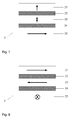
- a magnetic tunnel junction 2 is formed from an insulating layer 22 disposed between a reference layer 21, having a fixed magnetization direction, and a first storage layer 23, having a magnetization direction that is adjustable relative to the magnetization direction of the reference layer 21.
- the magnetic tunnel junction 2 further comprises a polarizing device for polarizing the spin of the electrons.
- the polarizing device is formed from a polarizing layer 25 and a non-magnetic spacer layer 24 separating the polarizing layer 25 from the first storage layer 23.
- the magnetization directions of the reference and first storage layers 21, 23 are oriented in-plane, i.e., in the plane of the respective reference and first storage layers 21, 23; while the polarizing layer 25 has a magnetization being oriented out-of-plane, i.e., in a plane that is perpendicular to the one of the polarizing layer 25, reference and first storage layers 21, 23.
- a magnetic element such as a memory or logic element
- a magnetic element can be formed by inserting the magnetic tunnel junction 2 between a current line connected, for example, to the junction 2 on the top of the reference layer 21, and a selection transistor connected, for example, to the bottom of the polarizing layer 25 and connected to and controllable via a word line.
- the current line is oriented in a different direction, preferably perpendicular, to the word line.
- a write operation data is written by applying a single write current pulse (not shown) through the magnetic tunnel junction 2, via the current line when the selection transistor is in the passing mode. More particularly, the electrons of the write current become polarized when passing through the polarizing magnetic layer 25 according to the current flow direction, so that the spins of the write current electrons penetrating into the first storage layer 23 are in majority oriented along the magnetization direction of the polarizing magnetic layer 25. When the amplitude of this spin-polarized write current is sufficient, the spins of the write current are capable of switching the magnetization direction of the first storage layer 23 by transfer of the angular spin moment between the spin-polarized carriers (electrons) and the magnetic moment of the first storage layer 23.
- spin transfer torque STT
- a perpendicular configuration such as the configuration of Fig. 1 , where the polarizing layer 25 has a magnetization oriented out-of-plane and perpendicular to the in-plane magnetization of the reference and first storage layers 21, 23, the electrons of the write current are polarized by the polarizing magnetic layer 25 with a direction perpendicular to the plane of the layers 21, 23.
- the magnetization of the first storage layer 23, when subjected to the write current with the so polarized spins, will then rotate within the plane of the first storage layer 23 in a precession mode.
- the magnetic element is formed by connecting the magnetic tunnel junction 2 between the word line, without the selection transistor, and the current line, or bit line, in the so-called cross-point configuration.
- An advantage of the magnetic element based on the magnetic tunnel junction 2 with the perpendicular configuration of Fig. 1 is a low write current density and a high writing speed.
- the rotation of the storage layer magnetization within the plane of the reference and first storage layers 21, 23 can have switching time of the magnetization in the sub-nanosecond range.
- the magnetization reversal taking place in conventional MRAM cells and written with a spin-transfer current is performed with a parallel configuration, where the spins of the write current are oriented in the plane of the first storage layer 23, or the magnetization layer to be switched.
- switching the storage layer magnetization is triggered by thermal activation being stochastic in nature, and the write operation speed is limited by switching times typically longer than 10 ns.
- the in-plane precession frequency f of the first storage layer magnetization can be expressed by Equation 1.
- Equation 1 J is the spin polarized write current, M s the saturation magnetization, t the thickness of the first storage layer 23 and ⁇ the gyromagnetic ratio (about 1.8 10 7 Oe -1 s -1 ), ⁇ is Planck's constant (1,05 10 -27 erg.s) and e the electron charge (4.8 10 -10 esu in CGS units).
- the symbol a J represents the amplitude of spin torque in magnetic field units, and g( ⁇ ) is the spin torque efficiency from Slonczewsky's model (see J. Magn. Magn.Mat.
- the intrinsic damping constant ⁇ has a value of typically about 0.01 in Co-based alloys usually used in magnetic tunnel junctions.
- Equation 2 The critical write current J c required for triggering the spin precession in the perpendicular configuration of Fig. 1 is given by Equation 2.
- J c 2 ⁇ e ⁇ M s ⁇ t g ⁇ / 2 ⁇ H K 2
- H K is the effective anisotropy field of the first storage layer 23, the effective anisotropy combining the shape anisotropy, magnetocrystalline anisotropy, and magnetoelastic anisotropy (if any) of the first storage layer 23. Therefore, the precession frequency f at the onset of the precession motion of the writing current spins is given by Equation 3.
- f ⁇ 2 ⁇ ⁇ ⁇ g ⁇ g ⁇ / 2 ⁇ H K 2
- Equation 3 yields a minimum precession frequency f varying between about 1 GHz to 10 GHz, depending upon the effective anisotropy H K , which is usually dominated by the shape anisotropy.
- This precession frequency range corresponds to characteristic switching time of the magnetization (half precession time constant) of about 500 ps to 50 ps, which is too fast for practical use in circuit design.
- Reducing the effective anisotropy H K can yield to a reduced thermal stability of the first storage layer 23. Indeed, in order to achieve thermal stability of the first storage layer magnetization against thermal fluctuations for a period of about 10 years, corresponding to the requested life time of a memory device, the criterion M s H k V > 100 k B T must be fulfilled, where V is the volume or dimension of the magnetic tunnel junction 2.
- the precession frequency f is independent from the saturation magnetization which is often used as a way to decrease the critical write current J c .
- the precession frequency f varies inversely with ⁇ .
- increasing the damping factor by a factor of ten allows decreasing the switching time of the magnetization in the range comprised between 1 ns to 30 ns. This range is practical for logic circuits design with nanosecond scale RC time constants.
- Gilbert damping constants are often derived from ferromagnetic resonance (FMR) experiments which involve small angle excitations of the magnetization, for example, typically of the order of a few degrees.
- FMR ferromagnetic resonance
- the precession angle is quite large, typically almost 90° and, additional spin-lattice relaxation phenomena, that are not necessarily present in FMR experiments, can take place.
- a material with large magnetic dissipation is likely to have a large effective damping for these large precession angles.
- Spin-lattice relaxation often takes place via spin-orbit coupling so that adding impurities having large spin orbit interactions (such as Pt, Pd, Au, rare earth impurities) can possibly increase the damping in magnetic materials.
- the first storage layer 23 is made of an alloy such as a Co, Fe, or Ni-based alloy with additions of one or several elements such as B, Ta, Cr, Zr, or Nb
- Fig. 2 taken from Reference Russek et. al., Journ. Appl. Phys. 91 (2002), p. 8659 .
- Fig. 3 shows the increase of Gilbert damping constant with Holmium impurities in a Ni80Fe20-based alloy, from Reference Benatmane et. al., J. Appl. Phys. 105, 07D314 (2009 ).
- impurity elements such as Pt, Pd, Ir, or Au can increase the Gilbert damping constant since these impurities have strong spin-orbit interactions.
- the first storage layer 23 can be made of a transition metal-based alloy, such a Co, Fe, or Ni-based alloy, preferentially comprising additions of one or several elements such as B, Ta, Cr, Zr, or Nb, and one or several rare earth impurities with large orbital moments such as Tb, Dy, Ho, and Er.
- the first storage layer 23 thus made has a Gilbert damping constant increasing with the rare earth impurity content as shown in Figs. 2 and 3 .
- the first storage layer 23 can be made to have a damping constant that is greater than 0.02, yielding switching time of the magnetization being greater than 1 ns.
- the damping constant of the storage layer 23 can be such that the switching time of the magnetization is in a range comprised between 1 ns and 100 ns, and preferably between 1 ns and 30 ns. This switching time range is practical for logic circuits design with nanosecond scale RC time constants.
- the magnetic tunnel junction 2 further comprises a second storage layer 230, adjacent to the first storage layer 23 and made of a material allowing for large magnetoresistance (TMR) amplitude, preferentially above 50%.
- the second storage layer 230 can be made of a transition metal-based alloy such a Co, Fe, or Ni-based alloy, preferentially comprising additions of one or several elements such as B, Ta, Cr, Zr, or Nb.
- the second storage layer 230 is in contact with the insulating layer 22.
- the first storage layer 23 can have a thickness comprised between 1 nm and 2nm, and can be made of an (NiFe) 96 Tb 4 alloy; while the second storage layer 230 can be made of a CoFeB alloy.
- the magnetic tunnel junction 2 further comprises a coupling layer, here, an antiferromagnetically coupling layer 231 disposed between the first storage layer 23 with the large damping constant and the second storage layer 230 having large TMR amplitude.
- the second storage layer 230 is in contact with the insulating layer 22.
- Such a configuration containing the first and second storage layers 23, 230 and the antiferromagnetically coupling layer 231 is also known as a synthetic antiferromagnetic free layer.
- the antiferromagnetically coupling layer 231 consists of a thin non magnetic layer; preferably a ruthenium layer with a thickness comprised between 0.6 nm and 0.9 nm, and provides the antiparallel (e.g. antiferromagnetic) coupling between the first and second storage layers 23, 230.
- the synthetic antiferromagnetic free layer configuration of Fig. 5 has a larger effective volume and thus, a better thermal stability.
- due to magnetic flux closure between the two antiparallel magnetization direction of the first and second storage layers 23, 230 the local magnetization within the first and second storage layers 23, 230, is more uniform, resulting in a more coherent switching of these two layers 23, 230.
- the magnetic tunnel junction 2 further comprises an antiferromagnetic layer 232 disposed between the first and second storage layers 23, 230.
- the antiferromagnetic layer 232 can typically be made of IrMn or PtMn and have a thickness in a range comprised between 0.5 nm and 2 nm. Due to its small thickness, the antiferromagnetic layer 232 cannot remain pinned upon switching the magnetization of the first and/or second storage layers 23, 230 and thus, cannot exchange bias these two storage layers 23, 230 at room temperature.
- the IrMn or PtMn material of the antiferromagnetic layer 232 has a large spin orbit interaction and, due to locally competing ferromagnetic and antiferromagnetic exchange interactions, a high degree of magnetic disorder exists at the interface between the antiferromagnetic layer 232 and the first and second storage layers 23, 230. Consequently, the coupling between the antiferromagnetic layer 232 and the first and second storage layers 23, 230 can generate a significant effective damping.
- the antiferromagnetic layer 232 can increase the thermal stability of the first and second storage layers 23, 230 at room temperature.
- the IrMn or PtMn alloys making the antiferromagnetic layer 232 usually have large magnetocrystalline anisotropy, and the overall anisotropy energy KV corresponds to the sum of the anisotropy energy KV of the first and second storage layers 23, 230, and of the antiferromagnetic layer 232.
- the first and second storage layers 23, 230 can thus be made thermally stable at smaller dimension, since larger anisotropy K allows fulfilling the criterion KV > 50 k B T for magnetic tunnel junctions 2 with a smaller dimension V.
- the write current pulse flowing through the magnetic tunnel junction 2 not only induces the transfer of the angular spin moment between the spin-polarized electrons and the magnetic moment of the first and second storage layers 23, 230, but also induces a temporary Joule heating of the magnetic tunnel junction 2.
- the Joule heating can reduce the anisotropy of the antiferromagnetic layer 232, possibly to zero in the case the temperature reach the Néel temperature.
- the switching of the magnetization of the first and second storage layers 23, 230 can be easier, while the first storage layers 23 has an enhanced damping compared to a configuration without the antiferromagnetic layer 232.
- the first and second storage layers 23, 230 are switched simultaneously according to the spin polarization of the write current and the write current polarity.
- a memory device (not shown) can be formed by assembling an array comprising a plurality of magnetic elements addressable by rows and columns, each magnetic element containing the magnetic tunnel junction 2 in accordance with the disclosed embodiments.
- the memory device comprises a plurality of the magnetic elements where the magnetic tunnel junction 2 of each magnetic element is connected to one selection transistor and one current line.
- each current line can address several magnetic tunnel junctions 2 in a row
- a word line (not shown) can address several selection transistors in a column.
- the current and word lines can be connected to the outputs of a row addressing circuit (not shown) and column addressing circuit (also not shown).
- several magnetic tunnel junctions 2 in a row can be addressed by the bit line, and several magnetic tunnel junctions 2 in a column can be addressed by the word line, as in the cross-point configuration.
- the polarizing layer 25 has a magnetization that is oriented in-plane and the reference and first storage layers 21, 23 have a magnetization respectively oriented out-of-plane.
- the spins of the write current are polarized with a spin precession direction that is in-plane and perpendicularly with the magnetization direction of the reference and first storage layers 21, 23.
- the damping constant of the first storage layer 23 can be intrinsically large due to the large perpendicular magnetocrystalline anisotropy required to maintain the magnetization of the first storage layer 23 out-of-plane.
- decreasing the damping constant while maintaining perpendicular anisotropy can be difficult.
- the polarizing layer 25 and the reference and first storage layers 21, 23 have a magnetization that is oriented in-plane.
- the magnetization of the polarizing layer 25 is shown entering the page and oriented perpendicular to the magnetization direction of the reference and first storage layers 21, 23.
- the spins of the write current are polarized in-plane with a spin precession direction that is perpendicular to the magnetization direction of the reference and storage layers 21, 23.
- the magnetic tunnel junction 2, and thus the memory device according to the embodiments disclosed herein allows using a write current that is smaller than the one used in conventional STT-based MRAM cells.
- the spins of the write current are polarized perpendicularly to the magnetization of the first storage layer 23 allowing for a decrease in the critical write current J c down to about 1 MA/cm 2 .
Abstract
Description
- The present disclosure relates to magnetic tunnel junction based magnetic element using a spin transfer torque (STT) write scheme in particular magnetic random memory (MRAM) cells or logic elements.
- In their simplest implementation, a magnetic random memory (MRAM) cell comprises a magnetic tunnel junction formed from a thin insulating layer sandwiched between a first magnetic layer, or reference layer, characterized by a fixed magnetization and a second magnetic layer, or storage layer, characterized by a magnetization which direction can be changed upon writing of the MRAM cell. When the respective magnetizations of the reference and storage layers are oriented antiparallel, the magnetic tunnel junction resistance is high (Rmax). On the other hand, when the respective magnetizations of the reference and storage layers are oriented parallel, the magnetic tunnel junction resistance becomes low (Rmin). The MRAM cell is read by comparing its junction resistance to the junction resistance of a reference cell, or several reference cells, Rref, having a junction resistance of Rref=(Rmin+Rmax)/2.
- It has also been proposed to use magnetic tunnel junctions in logic elements wherein the magnetic junction is used to store the results of the operation or to define the functionality of the logic element (see for instance "Fabrication of a Nonvolatile Full Adder Based on Logic-in-Memory Architecture Using Magnetic Tunnel Junctions" by Matsunaga et. al., Appl.Phys.Exp.1 (2008) 091301). The description below is described for MRAM element but it will be obvious for the man skilled in the art to translate it to logic type of applications.
- The MRAM cell can be written, by switching the magnetization direction of the storage layer, using different write operation schemes. In a first write operation scheme, two magnetic fields are applied coincidently in a cross-point architecture as described in
U.S. Patents No. 5,640,343 , No.6,430,085 and No.6,956,763 . This write operation scheme can be implemented in different manners that are known as magnetic field switching, Stoner-Wohlfarth Switching, Toggle Switching, Precessional switching, etc. - Alternatively, the MRAM cell can be written by a coincident magnetic field and a thermal pulse as described in
U.S. Patents No. 6,950,335 and No.6,535,416 . This approach is referred to as thermally assisted switching (TAS). - The MRAM cell can also be written using a spin polarized current flowing through the magnetic tunnel junction, as described initially in
U.S. Patents No. 5,695,864 and No.6,172,902 . As the spin polarized current acts as a local (magnetic) torque, this approach is known as spin transfer torque (STT). - Another possible write operation scheme includes a coincident pulse of spin polarized current flowing through the magnetic tunnel junction and a thermal heating current pulse as described in
U.S. Patent No. 6,950,335 . This approach is referred to as combined Spin transfer plus Thermally Assisted Switching (STT+TAS). - The write operation scheme based on STT is viewed as the most promising route for high density MRAM device using MRAM cells because the spin polarized write current scales directly with the MRAM cell size, which is not the case in the other write operation scheme implementations. In the STT-based write operation, the switching of the storage layer magnetization depends on the spin polarized current density which scales with the inverse of the area of the MRAM cell. Moreover, switching of the storage layer magnetization with the spin polarized current can be fast and the MRAM cell size can be minimized since no magnetic field line is required.
- Most practical implementations of the STT-based write operation so far involve a so-called "longitudinal" configuration, whereupon the spins of the spin polarized current are injected antiparallel (in the same plane or in-plane) as the storage layer magnetization to be switched. This can be done using storage layer materials having in-plane magnetization, i.e., having magnetization in the plane of the layers e.g. wafers, or perpendicular magnetization, e.g. having magnetization out of the plane of the magnetic wafers.
- MRAM cells with a STT-based write operation, however, suffers from several drawbacks. For example, the spin polarized write current density required to switch the storage layer magnetization is large (currently ∼4 MA/cm2 for a 10 ns pulse width) and increases dramatically for shorter pulse width. This leads to large and unpractical MRAM cell sizes due to underlying selection transistors sourcing such current densities. It also leads to high power dissipation and to a potential wear and correlated lack of reliability of the magnetic tunnel junction, in particular of the insulating layer.
- Moreover, insuring the stability of the data written in the MRAM cell by switching the magnetization of the storage layer requires achieving simultaneously good stability in the storage layer magnetization direction and a small write current in order to avoid the drawbacks above. This is becoming a major issue at feature sizes smaller than 45nm.
- Finally, the write operation speed is limited by the stochastic nature of switching. Indeed, if the intrinsic STT switching speed is fast (in the order of ns), the switching of the magnetization is triggered by thermal activation which is stochastic in nature. As a result, the practical switching time using the STT-based write operation is limited to about 10 ns or longer.
- The stability of written data can be improved using perpendicularly magnetized magnetic layers, as recently demonstrated by Nakayama et. al., Journ.Appl.Phys.103, 07A710 (2008). Alternatively, a good tradeoff between stability of written data and write current can be obtained by using a combination of TAS and STT, as proposed in
U.S. Patent No. 6,950,335 . None of these solutions, however, allows for a reduction in the write current density. - In order to decrease the write current density, several approaches have been proposed: more particularly,
U.S. Patent No. 6,603,677 proposes using a synthetic antiferromagnetic (SAF) multilayer as storage layer. The corresponding decrease of the current density is small (about 3 MA/cm2 at 10ns pulse width) but the true benefit is a more coherent internal magnetization in the magnetic cell, leading to a narrower current distribution within the magnetic cell array. - In their publication, Hayakawa et. al., Jap. Journ. Appl. Phys. 44 (2005) L1247, describes a method for decreasing the saturation magnetization of the storage layer. Here, the storage layer is assumed to be magnetized in-plane, and the write current scales directly with saturation magnetization. However, this approach has a severe drawback due to a sharp decrease of stability when the saturation magnetization is decreased caused by a correlative decrease of shape anisotropy. It is therefore not practical beyond a certain limit.
- U.S. Patent Application Publication
US2006/0141640 discloses using a dual magnetic tunnel junction structure, e.g. two symmetrical spin polarizing layer. This latter approach allows for using writing current in the order of 1 MA/cm2 for a 10ns pulse width but results in an increased complexity in the magnetic tunnel junction manufacturing process. - In an alternative approach,
U.S. Patent No. 6,532,164 discloses a MRAM cell configuration where the magnetic tunnel junction is formed from an insulating layer disposed between a first magnetic layer having a first magnetization direction, and a second magnetic layer having a second magnetization direction that is adjustable relative to the first magnetization direction. The magnetic tunnel junction also comprises a polarizing layer having a magnetization oriented perpendicular to the magnetization of the first and second magnetic layers. When a write current flows through the magnetic tunnel junction, the polarizing layer orients the spins of the write current perpendicularly to the magnetization of the first and second magnetic layers, and the write current switches the magnetization second magnetic layer through a precession of said magnetization in the plane of the magnetic layer. This configuration enables the use of a low write current density and permits an increased writing speed. However, in such a configuration, the second layer magnetization rotation frequency is in the range of 1 to 20 GHz (see Applied Physics Letters, 86 (2005), 022505) which is too high for any practical application such as in memory devices. Indeed, such high rotation frequencies would require a write current pulse in the sub-nanosecond range, which is too short in large arrays of MRAM cells with parasitic RC time constants. - The present application discloses a magnetic tunnel junction, magnetic element and memory device_which overcome at least some limitations of the prior art.
- According to the embodiments, a magnetic tunnel junction, can comprises a reference layer having a fixed magnetization direction, a first storage layer having a magnetization direction that is adjustable relative to the magnetization direction of the reference layer by passing a write current through said magnetic tunnel junction, and an insulating layer disposed between said reference layer and first storage layer; wherein the magnetic tunnel junction further comprises a polarizing device to polarize the spins of the write current oriented perpendicular with the magnetization direction of the reference layer; and wherein said first storage layer has a damping constant such that the switching time of the magnetization is in a range comprised between 1 ns and 100 ns.
- In an embodiment, said first storage layer has a damping constant above 0.02.
- In another embodiment, the polarizing device is a polarizing layer having a magnetization oriented perpendicular to the magnetization direction of the first storage layer.
- In yet another embodiment, the magnetization of said polarizing layer is oriented out of plane and the respective magnetizations of the reference and first storage layers are oriented in-plane.
- In yet another embodiment, the magnetization of said polarizing layer is oriented in-plane and the respective magnetizations of the reference and first storage layers are oriented out-of-plane.
- In yet another embodiment, the magnetization of said polarizing layer and the respective magnetizations of the reference and first storage layers are oriented in-plane but perpendicular to one another.
- In yet another embodiment, said first storage layer can be made from a transition metal-based alloy containing at least one element chosen from Pt, Pd, Ir, Au, or a rare earth element.
- In yet another embodiment, said at least one rare earth element is chosen from Sm, Tb, Gd, Er, or Ho.
- In yet another embodiment, said magnetic tunnel junction can further comprise a second storage layer having a magnetoresistance greater than 50%.
- In yet another embodiment, the magnetic tunnel junction can further comprise an antiferromagnetically coupling layer disposed between the first storage layer and the second storage layer and coupling antiferromagnetically said first and second storage layers.
- In yet another embodiment, the antiferromagnetically coupling layer can have a thickness comprised between 0.6 nm and 0.9 nm.
- In yet another embodiment, the magnetic tunnel junction can further comprise an antiferromagnetic layer having a thickness in a range comprised between 0.5 nm and 2 nm.
- The disclosure also pertains to a magnetic element, such as a memory or logic element, comprising the magnetic tunnel junction and being connected to a current line and a word line.
- In an embodiment, the word line can be connected to the magnetic tunnel junction via a selection transistor being controllable by the word line, and the current line can be adapted to pass a write current for switching the magnetization of said first storage layer when the selection transistor is in a passing mode.
- In another embodiment, a magnetic memory device comprises a plurality of the magnetic elements being addressable simultaneously by the current line in a row and by the world line in a column.
- The disclosed magnetic tunnel junction according to the embodiments disclosed herein allows using a write current with intensity down to 1 MA/cm2, and thus, obtaining a memory device, comprising the magnetic tunnel junction, having low overall power consumption. Due to low switching time of the storage layer of the disclosed magnetic tunnel junction, typically comprised between 1 and 100 ns, the disclosed junction has a faster write speed than the one in a conventional STT-MRAM cell.
- The preferred embodiments will be better understood with the aid of the description of an embodiment given by way of example and illustrated by the figures, in which:
-
Fig. 1 shows a magnetic tunnel junction comprising a reference layer, a storage layer and an insulating layer, according to an embodiment; -
Fig. 2 illustrates the increase of the damping constant as a function of rare earth element concentration in a Co, Fe, and Ni-based alloy; -
Fig. 3 shows the increase of damping constant as a function of Holmium concentration in a Ni80Fe20-based alloy; -
Fig. 4 illustrates the storage layer ofFig. 1 according to an embodiment; -
Fig. 5 illustrates the storage layer ofFig. 1 according to another embodiment; -
Fig. 6 represents the storage layer ofFig. 1 according to yet another embodiment; -
Fig. 7 shows the magnetic tunnel junction according to another embodiment; and -
Fig. 8 shows the magnetic tunnel junction according to yet another embodiment. - In an embodiment represented in
Fig. 1 , amagnetic tunnel junction 2 is formed from an insulatinglayer 22 disposed between areference layer 21, having a fixed magnetization direction, and afirst storage layer 23, having a magnetization direction that is adjustable relative to the magnetization direction of thereference layer 21. Themagnetic tunnel junction 2 further comprises a polarizing device for polarizing the spin of the electrons. In the example ofFig. 1 , the polarizing device is formed from apolarizing layer 25 and anon-magnetic spacer layer 24 separating thepolarizing layer 25 from thefirst storage layer 23. - In a preferred embodiment, the magnetization directions of the reference and first storage layers 21, 23 are oriented in-plane, i.e., in the plane of the respective reference and first storage layers 21, 23; while the
polarizing layer 25 has a magnetization being oriented out-of-plane, i.e., in a plane that is perpendicular to the one of thepolarizing layer 25, reference and first storage layers 21, 23. - In an embodiment not represented, a magnetic element, such as a memory or logic element, can be formed by inserting the
magnetic tunnel junction 2 between a current line connected, for example, to thejunction 2 on the top of thereference layer 21, and a selection transistor connected, for example, to the bottom of thepolarizing layer 25 and connected to and controllable via a word line. The current line is oriented in a different direction, preferably perpendicular, to the word line. - During a write operation, data is written by applying a single write current pulse (not shown) through the
magnetic tunnel junction 2, via the current line when the selection transistor is in the passing mode. More particularly, the electrons of the write current become polarized when passing through the polarizingmagnetic layer 25 according to the current flow direction, so that the spins of the write current electrons penetrating into thefirst storage layer 23 are in majority oriented along the magnetization direction of the polarizingmagnetic layer 25. When the amplitude of this spin-polarized write current is sufficient, the spins of the write current are capable of switching the magnetization direction of thefirst storage layer 23 by transfer of the angular spin moment between the spin-polarized carriers (electrons) and the magnetic moment of thefirst storage layer 23. This transfer of the angular spin is also known under the expression "spin transfer torque (STT)". In a perpendicular configuration, such as the configuration ofFig. 1 , where thepolarizing layer 25 has a magnetization oriented out-of-plane and perpendicular to the in-plane magnetization of the reference and first storage layers 21, 23, the electrons of the write current are polarized by the polarizingmagnetic layer 25 with a direction perpendicular to the plane of thelayers first storage layer 23, when subjected to the write current with the so polarized spins, will then rotate within the plane of thefirst storage layer 23 in a precession mode. - In another embodiment not represented, the magnetic element is formed by connecting the
magnetic tunnel junction 2 between the word line, without the selection transistor, and the current line, or bit line, in the so-called cross-point configuration. - Any other configurations of the magnetic element allowing for switching the magnetization direction of the
first storage layer 23 using the spin-polarized current are also possible. - An advantage of the magnetic element based on the
magnetic tunnel junction 2 with the perpendicular configuration ofFig. 1 is a low write current density and a high writing speed. Here, the rotation of the storage layer magnetization within the plane of the reference and first storage layers 21, 23 can have switching time of the magnetization in the sub-nanosecond range. In contrast, the magnetization reversal taking place in conventional MRAM cells and written with a spin-transfer current is performed with a parallel configuration, where the spins of the write current are oriented in the plane of thefirst storage layer 23, or the magnetization layer to be switched. In this parallel configuration, switching the storage layer magnetization is triggered by thermal activation being stochastic in nature, and the write operation speed is limited by switching times typically longer than 10 ns. - In the case of the perpendicular configuration of
Fig. 1 , the in-plane precession frequency f of the first storage layer magnetization can be expressed by Equation 1.
- In Equation 1, J is the spin polarized write current, Ms the saturation magnetization, t the thickness of the
first storage layer 23 and γ the gyromagnetic ratio (about 1.8 107 Oe-1s-1), ℏ is Planck's constant (1,05 10-27 erg.s) and e the electron charge (4.8 10-10 esu in CGS units). The symbol aJ represents the amplitude of spin torque in magnetic field units, and g(θ) is the spin torque efficiency from Slonczewsky's model (see J. Magn. Magn.Mat. 159 (1996) L1) which depends upon the angle θ between the polarization of the write current spins and the magnetization of the storage layer 23 (θ=π/2 in the perpendicular configuration). The intrinsic damping constant α has a value of typically about 0.01 in Co-based alloys usually used in magnetic tunnel junctions. - The critical write current Jc required for triggering the spin precession in the perpendicular configuration of
Fig. 1 is given byEquation 2.
- In
Equation 2, HK is the effective anisotropy field of thefirst storage layer 23, the effective anisotropy combining the shape anisotropy, magnetocrystalline anisotropy, and magnetoelastic anisotropy (if any) of thefirst storage layer 23. Therefore, the precession frequency f at the onset of the precession motion of the writing current spins is given by Equation 3.
- With usual materials parameters as described above, Equation 3 yields a minimum precession frequency f varying between about 1 GHz to 10 GHz, depending upon the effective anisotropy HK, which is usually dominated by the shape anisotropy. This precession frequency range corresponds to characteristic switching time of the magnetization (half precession time constant) of about 500 ps to 50 ps, which is too fast for practical use in circuit design.
- Reducing the effective anisotropy HK can yield to a reduced thermal stability of the
first storage layer 23. Indeed, in order to achieve thermal stability of the first storage layer magnetization against thermal fluctuations for a period of about 10 years, corresponding to the requested life time of a memory device, the criterion Ms Hk V > 100 kBT must be fulfilled, where V is the volume or dimension of themagnetic tunnel junction 2. - The precession frequency f is independent from the saturation magnetization which is often used as a way to decrease the critical write current Jc. The precession frequency f, however, varies inversely with α. Thus, increasing the damping factor by a factor of ten allows decreasing the switching time of the magnetization in the range comprised between 1 ns to 30 ns. This range is practical for logic circuits design with nanosecond scale RC time constants.
- Gilbert damping constants are often derived from ferromagnetic resonance (FMR) experiments which involve small angle excitations of the magnetization, for example, typically of the order of a few degrees. In the spin-torque induced precession motion described in the present disclosure, the precession angle is quite large, typically almost 90° and, additional spin-lattice relaxation phenomena, that are not necessarily present in FMR experiments, can take place. Nevertheless, a material with large magnetic dissipation (measured by the area of the hysteresis loop) is likely to have a large effective damping for these large precession angles. Spin-lattice relaxation often takes place via spin-orbit coupling so that adding impurities having large spin orbit interactions (such as Pt, Pd, Au, rare earth impurities) can possibly increase the damping in magnetic materials.
- For example, in the case the
first storage layer 23 is made of an alloy such as a Co, Fe, or Ni-based alloy with additions of one or several elements such as B, Ta, Cr, Zr, or Nb, it is possible to increase the Gilbert damping constant by adding rare earth impurities with large orbital moments such as Tb, Dy, Ho, Er, etc. This is illustrated onFig. 2 taken from Reference Russek et. al., Journ. Appl. Phys. 91 (2002), p. 8659.Fig. 3 shows the increase of Gilbert damping constant with Holmium impurities in a Ni80Fe20-based alloy, from Reference Benatmane et. al., J. Appl. Phys. 105, 07D314 (2009). - Similarly, the inclusion of impurity elements such as Pt, Pd, Ir, or Au can increase the Gilbert damping constant since these impurities have strong spin-orbit interactions.
- In the embodiment of
Fig. 1 , thefirst storage layer 23 can be made of a transition metal-based alloy, such a Co, Fe, or Ni-based alloy, preferentially comprising additions of one or several elements such as B, Ta, Cr, Zr, or Nb, and one or several rare earth impurities with large orbital moments such as Tb, Dy, Ho, and Er. Thefirst storage layer 23 thus made has a Gilbert damping constant increasing with the rare earth impurity content as shown inFigs. 2 and 3 . For example, thefirst storage layer 23 can be made to have a damping constant that is greater than 0.02, yielding switching time of the magnetization being greater than 1 ns. In an embodiment, the damping constant of thestorage layer 23 can be such that the switching time of the magnetization is in a range comprised between 1 ns and 100 ns, and preferably between 1 ns and 30 ns. This switching time range is practical for logic circuits design with nanosecond scale RC time constants. - In a preferred embodiment shown in
Fig. 4 , themagnetic tunnel junction 2 further comprises asecond storage layer 230, adjacent to thefirst storage layer 23 and made of a material allowing for large magnetoresistance (TMR) amplitude, preferentially above 50%. Thesecond storage layer 230 can be made of a transition metal-based alloy such a Co, Fe, or Ni-based alloy, preferentially comprising additions of one or several elements such as B, Ta, Cr, Zr, or Nb. Preferably, thesecond storage layer 230 is in contact with the insulatinglayer 22. In the example ofFig. 4 , thefirst storage layer 23 can have a thickness comprised between 1 nm and 2nm, and can be made of an (NiFe)96Tb4 alloy; while thesecond storage layer 230 can be made of a CoFeB alloy. - In another embodiment shown in
Fig. 5 , themagnetic tunnel junction 2 further comprises a coupling layer, here, anantiferromagnetically coupling layer 231 disposed between thefirst storage layer 23 with the large damping constant and thesecond storage layer 230 having large TMR amplitude. Preferably, thesecond storage layer 230 is in contact with the insulatinglayer 22. Such a configuration containing the first and second storage layers 23, 230 and theantiferromagnetically coupling layer 231 is also known as a synthetic antiferromagnetic free layer. Theantiferromagnetically coupling layer 231 consists of a thin non magnetic layer; preferably a ruthenium layer with a thickness comprised between 0.6 nm and 0.9 nm, and provides the antiparallel (e.g. antiferromagnetic) coupling between the first and second storage layers 23, 230. Compared to a single storage layer, the synthetic antiferromagnetic free layer configuration ofFig. 5 has a larger effective volume and thus, a better thermal stability. Moreover, due to magnetic flux closure between the two antiparallel magnetization direction of the first and second storage layers 23, 230, the local magnetization within the first and second storage layers 23, 230, is more uniform, resulting in a more coherent switching of these twolayers - In yet another embodiment represented in
Fig. 6 , themagnetic tunnel junction 2 further comprises anantiferromagnetic layer 232 disposed between the first and second storage layers 23, 230. Theantiferromagnetic layer 232 can typically be made of IrMn or PtMn and have a thickness in a range comprised between 0.5 nm and 2 nm. Due to its small thickness, theantiferromagnetic layer 232 cannot remain pinned upon switching the magnetization of the first and/or second storage layers 23, 230 and thus, cannot exchange bias these twostorage layers antiferromagnetic layer 232 has a large spin orbit interaction and, due to locally competing ferromagnetic and antiferromagnetic exchange interactions, a high degree of magnetic disorder exists at the interface between theantiferromagnetic layer 232 and the first and second storage layers 23, 230. Consequently, the coupling between theantiferromagnetic layer 232 and the first and second storage layers 23, 230 can generate a significant effective damping. - In the storage layer configuration of
Fig. 6 , theantiferromagnetic layer 232 can increase the thermal stability of the first and second storage layers 23, 230 at room temperature. Indeed, the IrMn or PtMn alloys making theantiferromagnetic layer 232 usually have large magnetocrystalline anisotropy, and the overall anisotropy energy KV corresponds to the sum of the anisotropy energy KV of the first and second storage layers 23, 230, and of theantiferromagnetic layer 232. The first and second storage layers 23, 230 can thus be made thermally stable at smaller dimension, since larger anisotropy K allows fulfilling the criterion KV > 50 kBT formagnetic tunnel junctions 2 with a smaller dimension V. - Furthermore, during the write operation, the write current pulse flowing through the
magnetic tunnel junction 2 not only induces the transfer of the angular spin moment between the spin-polarized electrons and the magnetic moment of the first and second storage layers 23, 230, but also induces a temporary Joule heating of themagnetic tunnel junction 2. In the configuration ofFig. 6 , the Joule heating can reduce the anisotropy of theantiferromagnetic layer 232, possibly to zero in the case the temperature reach the Néel temperature. In this case, the switching of the magnetization of the first and second storage layers 23, 230 can be easier, while the first storage layers 23 has an enhanced damping compared to a configuration without theantiferromagnetic layer 232. - During the write operation with the configuration of
Figs. 4 to 6 , the first and second storage layers 23, 230 are switched simultaneously according to the spin polarization of the write current and the write current polarity. - A memory device (not shown) can be formed by assembling an array comprising a plurality of magnetic elements addressable by rows and columns, each magnetic element containing the
magnetic tunnel junction 2 in accordance with the disclosed embodiments. - In an embodiment not represented, the memory device comprises a plurality of the magnetic elements where the
magnetic tunnel junction 2 of each magnetic element is connected to one selection transistor and one current line. In the memory device array, each current line can address severalmagnetic tunnel junctions 2 in a row, and a word line (not shown) can address several selection transistors in a column. The current and word lines can be connected to the outputs of a row addressing circuit (not shown) and column addressing circuit (also not shown). - Alternatively, in the memory device, several
magnetic tunnel junctions 2 in a row can be addressed by the bit line, and severalmagnetic tunnel junctions 2 in a column can be addressed by the word line, as in the cross-point configuration. - The disclosure is susceptible to various modifications and alternative forms, and specific examples thereof have been shown by way of example in the drawings and are herein described in detail. It should be understood, however, that the disclosure is not to be limited to the particular forms or methods disclosed, but to the contrary, the disclosure is to cover all modifications, equivalents, and alternatives.
- For example, in an embodiment represented in
Fig. 7 , thepolarizing layer 25 has a magnetization that is oriented in-plane and the reference and first storage layers 21, 23 have a magnetization respectively oriented out-of-plane. In the configuration ofFig. 7 , the spins of the write current are polarized with a spin precession direction that is in-plane and perpendicularly with the magnetization direction of the reference and first storage layers 21, 23. However, in such configuration, the damping constant of thefirst storage layer 23 can be intrinsically large due to the large perpendicular magnetocrystalline anisotropy required to maintain the magnetization of thefirst storage layer 23 out-of-plane. In the other hand, decreasing the damping constant while maintaining perpendicular anisotropy can be difficult. - In another embodiment represented in
Fig. 8 , thepolarizing layer 25 and the reference and first storage layers 21, 23 have a magnetization that is oriented in-plane. In the example ofFig. 8 , the magnetization of thepolarizing layer 25 is shown entering the page and oriented perpendicular to the magnetization direction of the reference and first storage layers 21, 23. Here, the spins of the write current are polarized in-plane with a spin precession direction that is perpendicular to the magnetization direction of the reference andstorage layers - The
magnetic tunnel junction 2, and thus the memory device according to the embodiments disclosed herein allows using a write current that is smaller than the one used in conventional STT-based MRAM cells. For example, in the perpendicular configuration ofFig. 1 , the spins of the write current are polarized perpendicularly to the magnetization of thefirst storage layer 23 allowing for a decrease in the critical write current Jc down to about 1 MA/cm2. -
- 2
- magnetic tunnel junction
- 21
- reference layer
- 22
- insulating layer
- 23
- first storage layer
- 24
- non-magnetic spacer layer
- 25
- magnetic polarizing layer
- 230
- second storage layer
- 231
- antiferromagnetically coupling layer
- 232
- antiferromagnetic layer
- aJ
- amplitude of spin torque
- e
- electron charge
- f
- precession frequency
- g(θ)
- spin torque efficiency
- J
- injected spin polarized current
- Jc
- critical write current
- kB
- Boltzmann constant
- KV
- anisotropy energy
- Ms
- saturation magnetization
- Rmax
- high magnetic tunnel junction resistance
- Rmin
- low magnetic tunnel junction resistance
- Rref
- junction resistance of a reference cell
- T
- temperature
- V
- volume
- α
- intrinsic damping constant
- ℏ
- Planck's constant
- θ
- angle between the injected spins and the local magnetization
Claims (15)
- A magnetic tunnel junction (2), comprising:a reference layer (21) having a fixed magnetization direction,a first storage layer (23) having a magnetization direction that is adjustable relative to the magnetization direction of the reference layer (21) by passing a write current through said magnetic tunnel junction (2), andan insulating layer (22) disposed between said reference layer (21) and first storage layer (23);characterized in thatthe magnetic tunnel junction (2) further comprises a polarizing device (25) to polarize the spins of the write current oriented perpendicular with the magnetization direction of the reference layer (21); and in thatsaid first storage layer (23) has a damping constant such that the switching time of the magnetization is in a range comprised between 1 ns and 100 ns.
- The magnetic tunnel junction (2) of claim 1, wherein said first storage layer (23) has a damping constant above 0.02.
- The magnetic tunnel junction (2) of the claims 1 or 2, wherein the polarizing device is a polarizing layer (25) having a magnetization oriented perpendicular to the magnetization direction of the first storage layer (23).
- The magnetic tunnel junction (2) of the claims 1 or 2, wherein the magnetization of said polarizing layer (25) is oriented out of plane and the respective magnetizations of the reference and first storage layers (21, 23) are oriented in-plane.
- The magnetic tunnel junction (2) of the claims 1 or 2, wherein the magnetization of said polarizing layer (25) is oriented in-plane and the respective magnetizations of the reference and first storage layers (21, 23) are oriented out-of-plane.
- The magnetic tunnel junction (2) of the claims 1 or 2, wherein the magnetization of said polarizing layer (25) and the respective magnetizations of the reference and first storage layers (21, 23) are oriented in-plane but perpendicular to one another.
- The magnetic tunnel junction (2) of any of the claims from 1 to 6, wherein
said first storage layer (23) is made from a transition metal-based alloy containing at least one element chosen from Pt, Pd, Ir, Au, or a rare earth element. - The magnetic tunnel junction (2) of claim 7, wherein
said at least one rare earth element is chosen from Sm, Tb, Gd, Er, or Ho. - The magnetic tunnel junction (2) of any of the claims from 1 to 8, wherein
said magnetic tunnel junction further comprises a second storage layer (230) allowing a magnetoresistance greater than 50%. - The magnetic tunnel junction (2) of claim 9,
further comprising an antiferromagnetically coupling layer (231) disposed between the first storage layer (23) and the second storage layer (230) and coupling antiferromagnetically said first and second storage layers (23, 230). - The magnetic tunnel junction (2) of claim 9,
further comprising an antiferromagnetic layer (232) having a thickness in a range comprised between 0.5 nm and 2 nm. - The magnetic tunnel junction (2) of claim 11, wherein
said antiferromagnetic layer (232) is made of an alloy chosen from IrMn or PtMn. - A magnetic element comprising the magnetic tunnel junction (2) characterized by any of the claims from 1 to 12 and being connected to a current line and a word line.
- The magnetic element of claim 13, wherein
said word line is connected to the magnetic tunnel junction (2) via a selection transistor being controllable by the word line, and wherein said current line being adapted to pass a write current for switching the magnetization of said first storage layer (23) when the selection transistor is in a passing mode. - A magnetic memory device comprising a plurality of magnetic elements, each magnetic element being characterized by the claims 13 or 14 and being addressable simultaneously by the current line in a row and by the world line in a column.
Applications Claiming Priority (1)
| Application Number | Priority Date | Filing Date | Title |
|---|---|---|---|
| US12/502,467 US8102703B2 (en) | 2009-07-14 | 2009-07-14 | Magnetic element with a fast spin transfer torque writing procedure |
Publications (2)
| Publication Number | Publication Date |
|---|---|
| EP2278589A1 true EP2278589A1 (en) | 2011-01-26 |
| EP2278589B1 EP2278589B1 (en) | 2014-04-23 |
Family
ID=42727663
Family Applications (1)
| Application Number | Title | Priority Date | Filing Date |
|---|---|---|---|
| EP10168719.2A Active EP2278589B1 (en) | 2009-07-14 | 2010-07-07 | Magnetic element with a fast spin transfer torque writing procedure |
Country Status (3)
| Country | Link |
|---|---|
| US (1) | US8102703B2 (en) |
| EP (1) | EP2278589B1 (en) |
| JP (1) | JP2011023722A (en) |
Cited By (4)
| Publication number | Priority date | Publication date | Assignee | Title |
|---|---|---|---|---|
| WO2014011533A1 (en) * | 2012-07-10 | 2014-01-16 | New York University | Precessional reversal in orthogonal spin transfer magnetic ram devices |
| FR3031622A1 (en) * | 2015-01-14 | 2016-07-15 | Centre Nat Rech Scient | MAGNETIC MEMORY POINT |
| US9818931B2 (en) | 2015-01-05 | 2017-11-14 | Samsung Electronics Co., Ltd. | Method and system for providing magnetic junctions using thermally assisted spin transfer torque switching |
| DE102012105595B4 (en) | 2011-08-10 | 2021-10-07 | Samsung Electronics Co. Ltd. | Magnetic tunnel junction devices, memories, storage systems and electronic devices |
Families Citing this family (16)
| Publication number | Priority date | Publication date | Assignee | Title |
|---|---|---|---|---|
| JP5644198B2 (en) * | 2010-06-15 | 2014-12-24 | ソニー株式会社 | Storage device |
| US8406045B1 (en) * | 2011-01-19 | 2013-03-26 | Grandis Inc. | Three terminal magnetic element |
| JP2012238631A (en) * | 2011-05-10 | 2012-12-06 | Sony Corp | Memory element and memory device |
| US9142758B2 (en) * | 2011-06-14 | 2015-09-22 | Samsung Electronics Co., Ltd. | Method and system for providing a magnetic junction configured for precessional switching using a bias structure |
| JP6117706B2 (en) * | 2012-01-04 | 2017-04-19 | トヨタ自動車株式会社 | Rare earth nanocomposite magnet |
| US9202562B2 (en) | 2012-04-18 | 2015-12-01 | Advanced Integrated Memory Inc. | Method to reduce read error rate for semiconductor resistive memory |
| US8773821B2 (en) * | 2012-10-05 | 2014-07-08 | Nve Corporation | Magnetoresistive-based mixed anisotropy high field sensor |
| US9343132B2 (en) * | 2013-05-22 | 2016-05-17 | Headway Technologies, Inc. | MRAM write pulses to dissipate intermediate state domains |
| US9344345B2 (en) * | 2014-03-19 | 2016-05-17 | Micron Technology, Inc. | Memory cells having a self-aligning polarizer |
| JP6331862B2 (en) * | 2014-08-08 | 2018-05-30 | 株式会社デンソー | Magnetoresistive element |
| US9524765B2 (en) * | 2014-08-15 | 2016-12-20 | Qualcomm Incorporated | Differential magnetic tunnel junction pair including a sense layer with a high coercivity portion |
| US9406365B1 (en) * | 2015-01-26 | 2016-08-02 | International Business Machines Corporation | Underlayers for textured films of Heusler compounds |
| CN110021699B (en) * | 2018-01-10 | 2023-06-02 | 中电海康集团有限公司 | Magnetic tunnel junction device and magnetic random access memory |
| CN111370571B (en) * | 2018-12-26 | 2022-09-20 | 中电海康集团有限公司 | Magnetic memory cell and SOT-MRAM memory |
| CN111370573B (en) * | 2018-12-26 | 2021-12-24 | 中电海康集团有限公司 | Magnetic memory cell and SOT-MRAM memory |
| CN113054096B (en) * | 2021-03-03 | 2024-03-19 | 南京大学 | Method for regulating and controlling intrinsic damping factor of magnetic film |
Citations (12)
| Publication number | Priority date | Publication date | Assignee | Title |
|---|---|---|---|---|
| US5640343A (en) | 1996-03-18 | 1997-06-17 | International Business Machines Corporation | Magnetic memory array using magnetic tunnel junction devices in the memory cells |
| US5695864A (en) | 1995-09-28 | 1997-12-09 | International Business Machines Corporation | Electronic device using magnetic components |
| US6172902B1 (en) | 1998-08-12 | 2001-01-09 | Ecole Polytechnique Federale De Lausanne (Epfl) | Non-volatile magnetic random access memory |
| US6430085B1 (en) | 2001-08-27 | 2002-08-06 | Motorola, Inc. | Magnetic random access memory having digit lines and bit lines with shape and induced anisotropy ferromagnetic cladding layer and method of manufacture |
| US6532164B2 (en) | 2000-12-07 | 2003-03-11 | Commissariat A L'energie Atomique | Magnetic spin polarization and magnetization rotation device with memory and writing process, using such a device |
| US6535416B1 (en) | 1999-06-18 | 2003-03-18 | Nve Corporation | Magnetic memory coincident thermal pulse data storage |
| US6603677B2 (en) | 2000-12-07 | 2003-08-05 | Commissariat A L'energie Atomique | Three-layered stacked magnetic spin polarization device with memory |
| US6950335B2 (en) | 2001-11-16 | 2005-09-27 | Commissariat A L'energie Atomique | Magnetic tunnel junction magnetic device, memory and writing and reading methods using said device |
| US6956763B2 (en) | 2003-06-27 | 2005-10-18 | Freescale Semiconductor, Inc. | MRAM element and methods for writing the MRAM element |
| US20060132990A1 (en) * | 2004-12-20 | 2006-06-22 | Kabushiki Kaisha Toshiba | Magnetic recording element, magnetic recording apparatus and recording method of information |
| US20060141640A1 (en) | 2004-12-29 | 2006-06-29 | Yiming Huai | MTJ elements with high spin polarization layers configured for spin-transfer switching and spintronics devices using the magnetic elements |
| WO2007013887A2 (en) * | 2004-10-15 | 2007-02-01 | The Trustees Of Columbia University In The City Of New York | Methods of manipulating the relaxation rate in magnetic materials and devices for using the same |
Family Cites Families (8)
| Publication number | Priority date | Publication date | Assignee | Title |
|---|---|---|---|---|
| US6602677B1 (en) | 1997-09-19 | 2003-08-05 | Promega Corporation | Thermostable luciferases and methods of production |
| FR2860910B1 (en) * | 2003-10-10 | 2006-02-10 | Commissariat Energie Atomique | MAGNETIC TUNNEL JUNCTION DEVICE AND METHOD OF WRITING / READING SUCH A DEVICE |
| JP4682585B2 (en) * | 2004-11-01 | 2011-05-11 | ソニー株式会社 | Memory element and memory |
| US7622784B2 (en) * | 2005-01-10 | 2009-11-24 | International Business Machines Corporation | MRAM device with improved stack structure and offset field for low-power toggle mode writing |
| US7154773B2 (en) * | 2005-03-31 | 2006-12-26 | Infineon Technologies Ag | MRAM cell with domain wall switching and field select |
| JP2008028362A (en) * | 2006-06-22 | 2008-02-07 | Toshiba Corp | Magnetoresistive element and magnetic memory |
| TWI449040B (en) * | 2006-10-06 | 2014-08-11 | Crocus Technology Sa | System and method for providing content-addressable magnetoresistive random access memory cells |
| FR2914482B1 (en) * | 2007-03-29 | 2009-05-29 | Commissariat Energie Atomique | MAGNETIC MEMORY WITH MAGNETIC TUNNEL JUNCTION |
-
2009
- 2009-07-14 US US12/502,467 patent/US8102703B2/en active Active
-
2010
- 2010-07-07 EP EP10168719.2A patent/EP2278589B1/en active Active
- 2010-07-13 JP JP2010158416A patent/JP2011023722A/en not_active Ceased
Patent Citations (12)
| Publication number | Priority date | Publication date | Assignee | Title |
|---|---|---|---|---|
| US5695864A (en) | 1995-09-28 | 1997-12-09 | International Business Machines Corporation | Electronic device using magnetic components |
| US5640343A (en) | 1996-03-18 | 1997-06-17 | International Business Machines Corporation | Magnetic memory array using magnetic tunnel junction devices in the memory cells |
| US6172902B1 (en) | 1998-08-12 | 2001-01-09 | Ecole Polytechnique Federale De Lausanne (Epfl) | Non-volatile magnetic random access memory |
| US6535416B1 (en) | 1999-06-18 | 2003-03-18 | Nve Corporation | Magnetic memory coincident thermal pulse data storage |
| US6532164B2 (en) | 2000-12-07 | 2003-03-11 | Commissariat A L'energie Atomique | Magnetic spin polarization and magnetization rotation device with memory and writing process, using such a device |
| US6603677B2 (en) | 2000-12-07 | 2003-08-05 | Commissariat A L'energie Atomique | Three-layered stacked magnetic spin polarization device with memory |
| US6430085B1 (en) | 2001-08-27 | 2002-08-06 | Motorola, Inc. | Magnetic random access memory having digit lines and bit lines with shape and induced anisotropy ferromagnetic cladding layer and method of manufacture |
| US6950335B2 (en) | 2001-11-16 | 2005-09-27 | Commissariat A L'energie Atomique | Magnetic tunnel junction magnetic device, memory and writing and reading methods using said device |
| US6956763B2 (en) | 2003-06-27 | 2005-10-18 | Freescale Semiconductor, Inc. | MRAM element and methods for writing the MRAM element |
| WO2007013887A2 (en) * | 2004-10-15 | 2007-02-01 | The Trustees Of Columbia University In The City Of New York | Methods of manipulating the relaxation rate in magnetic materials and devices for using the same |
| US20060132990A1 (en) * | 2004-12-20 | 2006-06-22 | Kabushiki Kaisha Toshiba | Magnetic recording element, magnetic recording apparatus and recording method of information |
| US20060141640A1 (en) | 2004-12-29 | 2006-06-29 | Yiming Huai | MTJ elements with high spin polarization layers configured for spin-transfer switching and spintronics devices using the magnetic elements |
Non-Patent Citations (5)
| Title |
|---|
| APPLIED PHYSICS LETTERS, vol. 86, 2005, pages 022505 |
| HAYAKAWA, JAP. JOURN. APPL. PHYS., vol. 44, 2005, pages L1247 |
| KISHI T ET AL: "Lower-current and fast switching of a perpendicular TMR for high speed and high density spin-transfer-torque MRAM", IEDM 2008. IEEE INTERNATIONAL ELECTRON DEVICES MEETING. TECHNICAL DIGEST IEEE PISCATAWAY, NJ, USA, INTERNATIONAL ELECTRON DEVICES MEETING. IEDM TECHNICAL DIGEST, 15 December 2008 (2008-12-15), pages 1 - 4, XP031434436, ISBN: 978-1-4244-2377-4 * |
| MATSUNAGA: "Fabrication of a Nonvolatile Full Adder Based on Logic-in-Memory Architecture Using Magnetic Tunnel Junctions", APPL.PHYS.EXP., vol. 1, 2008, pages 091301 |
| NAKAYAMA, JOURN.APPLPHYS., vol. 103, 2008, pages 07A710 |
Cited By (9)
| Publication number | Priority date | Publication date | Assignee | Title |
|---|---|---|---|---|
| DE102012105595B4 (en) | 2011-08-10 | 2021-10-07 | Samsung Electronics Co. Ltd. | Magnetic tunnel junction devices, memories, storage systems and electronic devices |
| WO2014011533A1 (en) * | 2012-07-10 | 2014-01-16 | New York University | Precessional reversal in orthogonal spin transfer magnetic ram devices |
| US8941196B2 (en) | 2012-07-10 | 2015-01-27 | New York University | Precessional reversal in orthogonal spin transfer magnetic RAM devices |
| US9818931B2 (en) | 2015-01-05 | 2017-11-14 | Samsung Electronics Co., Ltd. | Method and system for providing magnetic junctions using thermally assisted spin transfer torque switching |
| FR3031622A1 (en) * | 2015-01-14 | 2016-07-15 | Centre Nat Rech Scient | MAGNETIC MEMORY POINT |
| WO2016113503A1 (en) * | 2015-01-14 | 2016-07-21 | Centre National De La Recherche Scientifique | Magnetic memory slot |
| US20180005677A1 (en) * | 2015-01-14 | 2018-01-04 | Centre National De La Recherche Scientifique | Magnetic memory slot |
| JP2018508983A (en) * | 2015-01-14 | 2018-03-29 | セントレ・ナショナル・デ・ラ・レシェルシェ・サイエンティフィーク | Magnetic memory slot |
| US10224085B2 (en) * | 2015-01-14 | 2019-03-05 | Centre National De La Recherche Scientifique | Magnetic memory cell with asymmetrical geometry programmable by application of current in the absence of a magnetic field |
Also Published As
| Publication number | Publication date |
|---|---|
| JP2011023722A (en) | 2011-02-03 |
| US20110013448A1 (en) | 2011-01-20 |
| EP2278589B1 (en) | 2014-04-23 |
| US8102703B2 (en) | 2012-01-24 |
Similar Documents
| Publication | Publication Date | Title |
|---|---|---|
| EP2278589B1 (en) | Magnetic element with a fast spin transfer torque writing procedure | |
| US10460786B2 (en) | Systems and methods for reducing write error rate in magnetoelectric random access memory through pulse sharpening and reverse pulse schemes | |
| Apalkov et al. | Magnetoresistive random access memory | |
| US9812184B2 (en) | Current induced spin-momentum transfer stack with dual insulating layers | |
| US7486552B2 (en) | Method and system for providing a spin transfer device with improved switching characteristics | |
| US8208295B2 (en) | Heat assisted magnetic write element | |
| JP6328391B2 (en) | Magnetic tunneling junction using spin-orbit interaction based on switching and method and system for providing memory utilizing magnetic tunneling junction | |
| EP2446471B1 (en) | High speed low power magnetic devices based on current induced spin-momentum transfer | |
| US8279663B2 (en) | Magnetoresistance effect element and magnetic random access memory | |
| US7502253B2 (en) | Spin-transfer based MRAM with reduced critical current density | |
| US9230626B2 (en) | Electrically gated three-terminal circuits and devices based on spin hall torque effects in magnetic nanostructures apparatus, methods and applications | |
| US10475474B2 (en) | Storage element | |
| US9978931B2 (en) | Systems and methods for implementing robust magnetoelectric junctions | |
| US20170179372A1 (en) | Spin-orbit torque bit design for improved switching efficiency | |
| USRE49364E1 (en) | Memory element, memory apparatus | |
| EP2124228B1 (en) | Magnetic random access memory with an elliptical junction | |
| JP2012064904A (en) | Magnetoresistance effect element and magnetic random access memory | |
| Dieny et al. | Magnetic Random‐Access Memory | |
| CN103137854A (en) | Memory element and memory apparatus | |
| Bandiera et al. | Magnetic Random Access Memories | |
| Xiufeng et al. | Magnetic Random Access Memory |
Legal Events
| Date | Code | Title | Description |
|---|---|---|---|
| PUAI | Public reference made under article 153(3) epc to a published international application that has entered the european phase |
Free format text: ORIGINAL CODE: 0009012 |
|
| AK | Designated contracting states |
Kind code of ref document: A1 Designated state(s): AL AT BE BG CH CY CZ DE DK EE ES FI FR GB GR HR HU IE IS IT LI LT LU LV MC MK MT NL NO PL PT RO SE SI SK SM TR |
|
| AX | Request for extension of the european patent |
Extension state: BA ME RS |
|
| 17P | Request for examination filed |
Effective date: 20110624 |
|
| GRAP | Despatch of communication of intention to grant a patent |
Free format text: ORIGINAL CODE: EPIDOSNIGR1 |
|
| INTG | Intention to grant announced |
Effective date: 20131129 |
|
| GRAS | Grant fee paid |
Free format text: ORIGINAL CODE: EPIDOSNIGR3 |
|
| GRAA | (expected) grant |
Free format text: ORIGINAL CODE: 0009210 |
|
| AK | Designated contracting states |
Kind code of ref document: B1 Designated state(s): AL AT BE BG CH CY CZ DE DK EE ES FI FR GB GR HR HU IE IS IT LI LT LU LV MC MK MT NL NO PL PT RO SE SI SK SM TR |
|
| REG | Reference to a national code |
Ref country code: GB Ref legal event code: FG4D |
|
| REG | Reference to a national code |
Ref country code: CH Ref legal event code: EP |
|
| REG | Reference to a national code |
Ref country code: AT Ref legal event code: REF Ref document number: 664244 Country of ref document: AT Kind code of ref document: T Effective date: 20140515 |
|
| REG | Reference to a national code |
Ref country code: IE Ref legal event code: FG4D |
|
| REG | Reference to a national code |
Ref country code: DE Ref legal event code: R096 Ref document number: 602010015315 Country of ref document: DE Effective date: 20140605 |
|
| REG | Reference to a national code |
Ref country code: NL Ref legal event code: T3 |
|
| REG | Reference to a national code |
Ref country code: AT Ref legal event code: MK05 Ref document number: 664244 Country of ref document: AT Kind code of ref document: T Effective date: 20140423 |
|
| REG | Reference to a national code |
Ref country code: LT Ref legal event code: MG4D |
|
| PG25 | Lapsed in a contracting state [announced via postgrant information from national office to epo] |
Ref country code: CY Free format text: LAPSE BECAUSE OF FAILURE TO SUBMIT A TRANSLATION OF THE DESCRIPTION OR TO PAY THE FEE WITHIN THE PRESCRIBED TIME-LIMIT Effective date: 20140423 Ref country code: GR Free format text: LAPSE BECAUSE OF FAILURE TO SUBMIT A TRANSLATION OF THE DESCRIPTION OR TO PAY THE FEE WITHIN THE PRESCRIBED TIME-LIMIT Effective date: 20140724 Ref country code: FI Free format text: LAPSE BECAUSE OF FAILURE TO SUBMIT A TRANSLATION OF THE DESCRIPTION OR TO PAY THE FEE WITHIN THE PRESCRIBED TIME-LIMIT Effective date: 20140423 Ref country code: BG Free format text: LAPSE BECAUSE OF FAILURE TO SUBMIT A TRANSLATION OF THE DESCRIPTION OR TO PAY THE FEE WITHIN THE PRESCRIBED TIME-LIMIT Effective date: 20140723 Ref country code: NO Free format text: LAPSE BECAUSE OF FAILURE TO SUBMIT A TRANSLATION OF THE DESCRIPTION OR TO PAY THE FEE WITHIN THE PRESCRIBED TIME-LIMIT Effective date: 20140723 Ref country code: IS Free format text: LAPSE BECAUSE OF FAILURE TO SUBMIT A TRANSLATION OF THE DESCRIPTION OR TO PAY THE FEE WITHIN THE PRESCRIBED TIME-LIMIT Effective date: 20140823 Ref country code: LT Free format text: LAPSE BECAUSE OF FAILURE TO SUBMIT A TRANSLATION OF THE DESCRIPTION OR TO PAY THE FEE WITHIN THE PRESCRIBED TIME-LIMIT Effective date: 20140423 |
|
| PG25 | Lapsed in a contracting state [announced via postgrant information from national office to epo] |
Ref country code: SE Free format text: LAPSE BECAUSE OF FAILURE TO SUBMIT A TRANSLATION OF THE DESCRIPTION OR TO PAY THE FEE WITHIN THE PRESCRIBED TIME-LIMIT Effective date: 20140423 Ref country code: HR Free format text: LAPSE BECAUSE OF FAILURE TO SUBMIT A TRANSLATION OF THE DESCRIPTION OR TO PAY THE FEE WITHIN THE PRESCRIBED TIME-LIMIT Effective date: 20140423 Ref country code: LV Free format text: LAPSE BECAUSE OF FAILURE TO SUBMIT A TRANSLATION OF THE DESCRIPTION OR TO PAY THE FEE WITHIN THE PRESCRIBED TIME-LIMIT Effective date: 20140423 Ref country code: ES Free format text: LAPSE BECAUSE OF FAILURE TO SUBMIT A TRANSLATION OF THE DESCRIPTION OR TO PAY THE FEE WITHIN THE PRESCRIBED TIME-LIMIT Effective date: 20140423 Ref country code: PL Free format text: LAPSE BECAUSE OF FAILURE TO SUBMIT A TRANSLATION OF THE DESCRIPTION OR TO PAY THE FEE WITHIN THE PRESCRIBED TIME-LIMIT Effective date: 20140423 Ref country code: AT Free format text: LAPSE BECAUSE OF FAILURE TO SUBMIT A TRANSLATION OF THE DESCRIPTION OR TO PAY THE FEE WITHIN THE PRESCRIBED TIME-LIMIT Effective date: 20140423 |
|
| PG25 | Lapsed in a contracting state [announced via postgrant information from national office to epo] |
Ref country code: PT Free format text: LAPSE BECAUSE OF FAILURE TO SUBMIT A TRANSLATION OF THE DESCRIPTION OR TO PAY THE FEE WITHIN THE PRESCRIBED TIME-LIMIT Effective date: 20140825 |
|
| REG | Reference to a national code |
Ref country code: DE Ref legal event code: R097 Ref document number: 602010015315 Country of ref document: DE |
|
| PG25 | Lapsed in a contracting state [announced via postgrant information from national office to epo] |
Ref country code: RO Free format text: LAPSE BECAUSE OF FAILURE TO SUBMIT A TRANSLATION OF THE DESCRIPTION OR TO PAY THE FEE WITHIN THE PRESCRIBED TIME-LIMIT Effective date: 20140423 Ref country code: CZ Free format text: LAPSE BECAUSE OF FAILURE TO SUBMIT A TRANSLATION OF THE DESCRIPTION OR TO PAY THE FEE WITHIN THE PRESCRIBED TIME-LIMIT Effective date: 20140423 Ref country code: DK Free format text: LAPSE BECAUSE OF FAILURE TO SUBMIT A TRANSLATION OF THE DESCRIPTION OR TO PAY THE FEE WITHIN THE PRESCRIBED TIME-LIMIT Effective date: 20140423 Ref country code: BE Free format text: LAPSE BECAUSE OF FAILURE TO SUBMIT A TRANSLATION OF THE DESCRIPTION OR TO PAY THE FEE WITHIN THE PRESCRIBED TIME-LIMIT Effective date: 20140423 Ref country code: EE Free format text: LAPSE BECAUSE OF FAILURE TO SUBMIT A TRANSLATION OF THE DESCRIPTION OR TO PAY THE FEE WITHIN THE PRESCRIBED TIME-LIMIT Effective date: 20140423 Ref country code: SK Free format text: LAPSE BECAUSE OF FAILURE TO SUBMIT A TRANSLATION OF THE DESCRIPTION OR TO PAY THE FEE WITHIN THE PRESCRIBED TIME-LIMIT Effective date: 20140423 |
|
| PG25 | Lapsed in a contracting state [announced via postgrant information from national office to epo] |
Ref country code: LU Free format text: LAPSE BECAUSE OF FAILURE TO SUBMIT A TRANSLATION OF THE DESCRIPTION OR TO PAY THE FEE WITHIN THE PRESCRIBED TIME-LIMIT Effective date: 20140707 |
|
| PLBE | No opposition filed within time limit |
Free format text: ORIGINAL CODE: 0009261 |
|
| REG | Reference to a national code |
Ref country code: CH Ref legal event code: PL |
|
| STAA | Information on the status of an ep patent application or granted ep patent |
Free format text: STATUS: NO OPPOSITION FILED WITHIN TIME LIMIT |
|
| PG25 | Lapsed in a contracting state [announced via postgrant information from national office to epo] |
Ref country code: IT Free format text: LAPSE BECAUSE OF FAILURE TO SUBMIT A TRANSLATION OF THE DESCRIPTION OR TO PAY THE FEE WITHIN THE PRESCRIBED TIME-LIMIT Effective date: 20140423 |
|
| 26N | No opposition filed |
Effective date: 20150126 |
|
| REG | Reference to a national code |
Ref country code: IE Ref legal event code: MM4A |
|
| PG25 | Lapsed in a contracting state [announced via postgrant information from national office to epo] |
Ref country code: CH Free format text: LAPSE BECAUSE OF NON-PAYMENT OF DUE FEES Effective date: 20140731 Ref country code: LI Free format text: LAPSE BECAUSE OF NON-PAYMENT OF DUE FEES Effective date: 20140731 |
|
| REG | Reference to a national code |
Ref country code: DE Ref legal event code: R097 Ref document number: 602010015315 Country of ref document: DE Effective date: 20150126 |
|
| REG | Reference to a national code |
Ref country code: FR Ref legal event code: PLFP Year of fee payment: 6 |
|
| PG25 | Lapsed in a contracting state [announced via postgrant information from national office to epo] |
Ref country code: SI Free format text: LAPSE BECAUSE OF FAILURE TO SUBMIT A TRANSLATION OF THE DESCRIPTION OR TO PAY THE FEE WITHIN THE PRESCRIBED TIME-LIMIT Effective date: 20140423 |
|
| PG25 | Lapsed in a contracting state [announced via postgrant information from national office to epo] |
Ref country code: IE Free format text: LAPSE BECAUSE OF NON-PAYMENT OF DUE FEES Effective date: 20140707 |
|
| REG | Reference to a national code |
Ref country code: FR Ref legal event code: GC Effective date: 20151118 |
|
| PG25 | Lapsed in a contracting state [announced via postgrant information from national office to epo] |
Ref country code: SM Free format text: LAPSE BECAUSE OF FAILURE TO SUBMIT A TRANSLATION OF THE DESCRIPTION OR TO PAY THE FEE WITHIN THE PRESCRIBED TIME-LIMIT Effective date: 20140423 Ref country code: MC Free format text: LAPSE BECAUSE OF FAILURE TO SUBMIT A TRANSLATION OF THE DESCRIPTION OR TO PAY THE FEE WITHIN THE PRESCRIBED TIME-LIMIT Effective date: 20140423 |
|
| PG25 | Lapsed in a contracting state [announced via postgrant information from national office to epo] |
Ref country code: MT Free format text: LAPSE BECAUSE OF FAILURE TO SUBMIT A TRANSLATION OF THE DESCRIPTION OR TO PAY THE FEE WITHIN THE PRESCRIBED TIME-LIMIT Effective date: 20140423 |
|
| REG | Reference to a national code |
Ref country code: FR Ref legal event code: PLFP Year of fee payment: 7 |
|
| PG25 | Lapsed in a contracting state [announced via postgrant information from national office to epo] |
Ref country code: TR Free format text: LAPSE BECAUSE OF FAILURE TO SUBMIT A TRANSLATION OF THE DESCRIPTION OR TO PAY THE FEE WITHIN THE PRESCRIBED TIME-LIMIT Effective date: 20140423 Ref country code: HU Free format text: LAPSE BECAUSE OF FAILURE TO SUBMIT A TRANSLATION OF THE DESCRIPTION OR TO PAY THE FEE WITHIN THE PRESCRIBED TIME-LIMIT; INVALID AB INITIO Effective date: 20100707 |
|
| PGFP | Annual fee paid to national office [announced via postgrant information from national office to epo] |
Ref country code: NL Payment date: 20160720 Year of fee payment: 7 |
|
| REG | Reference to a national code |
Ref country code: FR Ref legal event code: PLFP Year of fee payment: 8 |
|
| REG | Reference to a national code |
Ref country code: NL Ref legal event code: MM Effective date: 20170801 |
|
| PG25 | Lapsed in a contracting state [announced via postgrant information from national office to epo] |
Ref country code: NL Free format text: LAPSE BECAUSE OF NON-PAYMENT OF DUE FEES Effective date: 20170801 |
|
| PG25 | Lapsed in a contracting state [announced via postgrant information from national office to epo] |
Ref country code: MK Free format text: LAPSE BECAUSE OF FAILURE TO SUBMIT A TRANSLATION OF THE DESCRIPTION OR TO PAY THE FEE WITHIN THE PRESCRIBED TIME-LIMIT Effective date: 20140423 |
|
| REG | Reference to a national code |
Ref country code: FR Ref legal event code: PLFP Year of fee payment: 9 |
|
| PG25 | Lapsed in a contracting state [announced via postgrant information from national office to epo] |
Ref country code: AL Free format text: LAPSE BECAUSE OF FAILURE TO SUBMIT A TRANSLATION OF THE DESCRIPTION OR TO PAY THE FEE WITHIN THE PRESCRIBED TIME-LIMIT Effective date: 20140423 |
|
| REG | Reference to a national code |
Ref country code: DE Ref legal event code: R082 Ref document number: 602010015315 Country of ref document: DE Representative=s name: BECK & ROESSIG EUROPEAN PATENT ATTORNEYS, DE Ref country code: DE Ref legal event code: R082 Ref document number: 602010015315 Country of ref document: DE Representative=s name: BECK & ROESSIG - EUROPEAN PATENT ATTORNEYS, DE |
|
| P01 | Opt-out of the competence of the unified patent court (upc) registered |
Effective date: 20230620 |
|
| REG | Reference to a national code |
Ref country code: DE Ref legal event code: R081 Ref document number: 602010015315 Country of ref document: DE Owner name: CROCUS TECHNOLOGY SA, FR Free format text: FORMER OWNER: CROCUS TECHNOLOGY, GRENOBLE, FR Ref country code: DE Ref legal event code: R081 Ref document number: 602010015315 Country of ref document: DE Owner name: ALLEGRO MICRO SYSTEMS LLC, MANCHESTER, US Free format text: FORMER OWNER: CROCUS TECHNOLOGY, GRENOBLE, FR Ref country code: DE Ref legal event code: R081 Ref document number: 602010015315 Country of ref document: DE Owner name: ALLEGRO MICRO SYSTEMS LLC, WILMINGTON, US Free format text: FORMER OWNER: CROCUS TECHNOLOGY, GRENOBLE, FR |
|
| PGFP | Annual fee paid to national office [announced via postgrant information from national office to epo] |
Ref country code: GB Payment date: 20230720 Year of fee payment: 14 |
|
| PGFP | Annual fee paid to national office [announced via postgrant information from national office to epo] |
Ref country code: FR Payment date: 20230725 Year of fee payment: 14 Ref country code: DE Payment date: 20230719 Year of fee payment: 14 |
|
| REG | Reference to a national code |
Ref country code: DE Ref legal event code: R081 Ref document number: 602010015315 Country of ref document: DE Owner name: ALLEGRO MICRO SYSTEMS LLC, MANCHESTER, US Free format text: FORMER OWNER: CROCUS TECHNOLOGY SA, GRENOBLE, FR Ref country code: DE Ref legal event code: R081 Ref document number: 602010015315 Country of ref document: DE Owner name: ALLEGRO MICRO SYSTEMS LLC, WILMINGTON, US Free format text: FORMER OWNER: CROCUS TECHNOLOGY SA, GRENOBLE, FR |
|
| REG | Reference to a national code |
Ref country code: DE Ref legal event code: R081 Ref document number: 602010015315 Country of ref document: DE Owner name: ALLEGRO MICRO SYSTEMS LLC, MANCHESTER, US Free format text: FORMER OWNER: ALLEGRO MICRO SYSTEMS LLC, WILMINGTON, DE, US |
|
| REG | Reference to a national code |
Ref country code: GB Ref legal event code: 732E Free format text: REGISTERED BETWEEN 20240229 AND 20240306 |