EP2284962A2 - Electrical connectors with air-circulation and polarization features - Google Patents
Electrical connectors with air-circulation and polarization features Download PDFInfo
- Publication number
- EP2284962A2 EP2284962A2 EP10187346A EP10187346A EP2284962A2 EP 2284962 A2 EP2284962 A2 EP 2284962A2 EP 10187346 A EP10187346 A EP 10187346A EP 10187346 A EP10187346 A EP 10187346A EP 2284962 A2 EP2284962 A2 EP 2284962A2
- Authority
- EP
- European Patent Office
- Prior art keywords
- power contact
- housing
- cavity
- contact
- electrical connector
- Prior art date
- Legal status (The legal status is an assumption and is not a legal conclusion. Google has not performed a legal analysis and makes no representation as to the accuracy of the status listed.)
- Withdrawn
Links
Images


Classifications
-
- H—ELECTRICITY
- H01—ELECTRIC ELEMENTS
- H01R—ELECTRICALLY-CONDUCTIVE CONNECTIONS; STRUCTURAL ASSOCIATIONS OF A PLURALITY OF MUTUALLY-INSULATED ELECTRICAL CONNECTING ELEMENTS; COUPLING DEVICES; CURRENT COLLECTORS
- H01R13/00—Details of coupling devices of the kinds covered by groups H01R12/70 or H01R24/00 - H01R33/00
- H01R13/64—Means for preventing incorrect coupling
-
- H—ELECTRICITY
- H01—ELECTRIC ELEMENTS
- H01R—ELECTRICALLY-CONDUCTIVE CONNECTIONS; STRUCTURAL ASSOCIATIONS OF A PLURALITY OF MUTUALLY-INSULATED ELECTRICAL CONNECTING ELEMENTS; COUPLING DEVICES; CURRENT COLLECTORS
- H01R12/00—Structural associations of a plurality of mutually-insulated electrical connecting elements, specially adapted for printed circuits, e.g. printed circuit boards [PCB], flat or ribbon cables, or like generally planar structures, e.g. terminal strips, terminal blocks; Coupling devices specially adapted for printed circuits, flat or ribbon cables, or like generally planar structures; Terminals specially adapted for contact with, or insertion into, printed circuits, flat or ribbon cables, or like generally planar structures
- H01R12/70—Coupling devices
- H01R12/7088—Arrangements for power supply
-
- H—ELECTRICITY
- H01—ELECTRIC ELEMENTS
- H01R—ELECTRICALLY-CONDUCTIVE CONNECTIONS; STRUCTURAL ASSOCIATIONS OF A PLURALITY OF MUTUALLY-INSULATED ELECTRICAL CONNECTING ELEMENTS; COUPLING DEVICES; CURRENT COLLECTORS
- H01R12/00—Structural associations of a plurality of mutually-insulated electrical connecting elements, specially adapted for printed circuits, e.g. printed circuit boards [PCB], flat or ribbon cables, or like generally planar structures, e.g. terminal strips, terminal blocks; Coupling devices specially adapted for printed circuits, flat or ribbon cables, or like generally planar structures; Terminals specially adapted for contact with, or insertion into, printed circuits, flat or ribbon cables, or like generally planar structures
- H01R12/50—Fixed connections
- H01R12/51—Fixed connections for rigid printed circuits or like structures
-
- H—ELECTRICITY
- H01—ELECTRIC ELEMENTS
- H01R—ELECTRICALLY-CONDUCTIVE CONNECTIONS; STRUCTURAL ASSOCIATIONS OF A PLURALITY OF MUTUALLY-INSULATED ELECTRICAL CONNECTING ELEMENTS; COUPLING DEVICES; CURRENT COLLECTORS
- H01R12/00—Structural associations of a plurality of mutually-insulated electrical connecting elements, specially adapted for printed circuits, e.g. printed circuit boards [PCB], flat or ribbon cables, or like generally planar structures, e.g. terminal strips, terminal blocks; Coupling devices specially adapted for printed circuits, flat or ribbon cables, or like generally planar structures; Terminals specially adapted for contact with, or insertion into, printed circuits, flat or ribbon cables, or like generally planar structures
- H01R12/70—Coupling devices
- H01R12/71—Coupling devices for rigid printing circuits or like structures
- H01R12/712—Coupling devices for rigid printing circuits or like structures co-operating with the surface of the printed circuit or with a coupling device exclusively provided on the surface of the printed circuit
- H01R12/716—Coupling device provided on the PCB
-
- H—ELECTRICITY
- H01—ELECTRIC ELEMENTS
- H01R—ELECTRICALLY-CONDUCTIVE CONNECTIONS; STRUCTURAL ASSOCIATIONS OF A PLURALITY OF MUTUALLY-INSULATED ELECTRICAL CONNECTING ELEMENTS; COUPLING DEVICES; CURRENT COLLECTORS
- H01R12/00—Structural associations of a plurality of mutually-insulated electrical connecting elements, specially adapted for printed circuits, e.g. printed circuit boards [PCB], flat or ribbon cables, or like generally planar structures, e.g. terminal strips, terminal blocks; Coupling devices specially adapted for printed circuits, flat or ribbon cables, or like generally planar structures; Terminals specially adapted for contact with, or insertion into, printed circuits, flat or ribbon cables, or like generally planar structures
- H01R12/70—Coupling devices
- H01R12/71—Coupling devices for rigid printing circuits or like structures
- H01R12/72—Coupling devices for rigid printing circuits or like structures coupling with the edge of the rigid printed circuits or like structures
- H01R12/722—Coupling devices for rigid printing circuits or like structures coupling with the edge of the rigid printed circuits or like structures coupling devices mounted on the edge of the printed circuits
- H01R12/724—Coupling devices for rigid printing circuits or like structures coupling with the edge of the rigid printed circuits or like structures coupling devices mounted on the edge of the printed circuits containing contact members forming a right angle
-
- H—ELECTRICITY
- H01—ELECTRIC ELEMENTS
- H01R—ELECTRICALLY-CONDUCTIVE CONNECTIONS; STRUCTURAL ASSOCIATIONS OF A PLURALITY OF MUTUALLY-INSULATED ELECTRICAL CONNECTING ELEMENTS; COUPLING DEVICES; CURRENT COLLECTORS
- H01R12/00—Structural associations of a plurality of mutually-insulated electrical connecting elements, specially adapted for printed circuits, e.g. printed circuit boards [PCB], flat or ribbon cables, or like generally planar structures, e.g. terminal strips, terminal blocks; Coupling devices specially adapted for printed circuits, flat or ribbon cables, or like generally planar structures; Terminals specially adapted for contact with, or insertion into, printed circuits, flat or ribbon cables, or like generally planar structures
- H01R12/70—Coupling devices
- H01R12/71—Coupling devices for rigid printing circuits or like structures
- H01R12/72—Coupling devices for rigid printing circuits or like structures coupling with the edge of the rigid printed circuits or like structures
- H01R12/73—Coupling devices for rigid printing circuits or like structures coupling with the edge of the rigid printed circuits or like structures connecting to other rigid printed circuits or like structures
- H01R12/735—Printed circuits including an angle between each other
- H01R12/737—Printed circuits being substantially perpendicular to each other
-
- H—ELECTRICITY
- H01—ELECTRIC ELEMENTS
- H01R—ELECTRICALLY-CONDUCTIVE CONNECTIONS; STRUCTURAL ASSOCIATIONS OF A PLURALITY OF MUTUALLY-INSULATED ELECTRICAL CONNECTING ELEMENTS; COUPLING DEVICES; CURRENT COLLECTORS
- H01R13/00—Details of coupling devices of the kinds covered by groups H01R12/70 or H01R24/00 - H01R33/00
- H01R13/40—Securing contact members in or to a base or case; Insulating of contact members
- H01R13/42—Securing in a demountable manner
-
- H—ELECTRICITY
- H01—ELECTRIC ELEMENTS
- H01R—ELECTRICALLY-CONDUCTIVE CONNECTIONS; STRUCTURAL ASSOCIATIONS OF A PLURALITY OF MUTUALLY-INSULATED ELECTRICAL CONNECTING ELEMENTS; COUPLING DEVICES; CURRENT COLLECTORS
- H01R13/00—Details of coupling devices of the kinds covered by groups H01R12/70 or H01R24/00 - H01R33/00
- H01R13/64—Means for preventing incorrect coupling
- H01R13/642—Means for preventing incorrect coupling by position or shape of contact members
-
- H—ELECTRICITY
- H01—ELECTRIC ELEMENTS
- H01R—ELECTRICALLY-CONDUCTIVE CONNECTIONS; STRUCTURAL ASSOCIATIONS OF A PLURALITY OF MUTUALLY-INSULATED ELECTRICAL CONNECTING ELEMENTS; COUPLING DEVICES; CURRENT COLLECTORS
- H01R13/00—Details of coupling devices of the kinds covered by groups H01R12/70 or H01R24/00 - H01R33/00
- H01R13/648—Protective earth or shield arrangements on coupling devices, e.g. anti-static shielding
Definitions
- the present invention relates to electrical connectors for transmitting electrical power.
- Assembling contacts into a connector housing can also be problematic. Contacts can be inserted into improper cavities or only partially inserted into a cavity.
- Embodiments of electrical connectors include features that facilitate circulation of air through and around the electrical connectors.
- the air can cool the power contacts of the electrical connectors, thereby allowing the power contacts to operate at higher currents that would otherwise be possible.
- Features are also included to help prevent mis-insertion or partial insertion of contacts into a housing.
- Embodiments of connector systems comprise a first electrical connector comprising an electrically-insulative housing that defines a cavity.
- the housing has an aperture formed therein that places the cavity in fluid communication with the environment around the first electrical connector.
- the first electrical connector also comprises a power contact having a mating portion located in the cavity.
- the connector system also comprises a second electrical connector that mates with the first electrical connector.
- the second electrical connector comprises an electrically-insulative housing that defines a cavity.
- the housing of the second electrical connector has an aperture formed therein that places the cavity of the second electrical connector in fluid communication with the environment around the second electrical connector.
- the second electrical connector also comprises a power contact having a mating portion located in the cavity of the housing of the second electrical connector.
- the apertures formed in the housings of the first and second electrical connectors overlap when the first and second electrical connectors are mated.
- Embodiments of electrical connectors for mounting on a substrate comprise a power contact and an electrically insulative housing that receives the power contact.
- An aperture is formed in the housing. The aperture is aligned with a mating portion of power contact whereby air heated by the power contact can exit the power contact by way of the aperture.
- a recess is formed in the housing. The recess faces the substrate, and the recess and the substrate define a passage extending from a side portion of the housing when the electrical connector is mounted on the substrate. A portion of the power contact extends through the recess, whereby air from the environment around the electrical connector can pass between the housing and substrate and over the power contact.
- Embodiments of electrical connectors comprise an electrically insulative housing, and a power contact mounted in the housing and having a mating portion.
- the housing has an aperture formed therein and aligned with the mating portion of the contact whereby air heated by the power contact can exit the power contact by way of the aperture.
- Embodiments of electrical connectors include a housing and two different types of power contacts.
- the power contacts include polarizing features that reduce or eliminate the potential for the power contacts to be improperly installed in the housing.
- Embodiments of electrical connectors comprise a first power contact comprising a tab; a second power contact comprising a tab; and a housing having a first and a second cavity formed therein that receive the respective first and second power contacts.
- the tab of the first power contact interferedly contacts the housing when the first power contact is partially inserted into the second cavity thereby preventing installation of the first power contact in the second cavity.
- the tab of the second power contact interferedly contacts the housing when the second power contact is partially inserted into the first cavity thereby preventing installation of the second power contact in the first cavity.
- Figure 1 is a top perspective view of a preferred embodiment of a connector system depicting a header connector and a receptacle connector of the connector system in a fully mated condition;
- Figure 2 is a side view of the connector system shown in Figure 1 , depicting the header connector and the receptacle connector in the fully mated condition;
- Figure 3 is a top perspective view of the connector system shown in Figures 1 and 2 , depicting the header connector and the receptacle connector an unmated condition;
- Figure 4 is a top perspective view of the connector system shown in Figures 1-3 , depicting the header connector and the receptacle connector the unmated condition;
- Figure 5 is top view of the connector system shown in Figures 1-4 , depicting the header connector and the receptacle connector in a partially mated condition;
- Figure 6 is a magnified, partial cutaway view of the area designated "A" in Figure 5 ;
- Figure 7 is top view of the connector system shown in Figures 1-6 , depicting the header connector and the receptacle connector in the fully mated condition;
- Figure 8 is a magnified, partial cutaway view of the area designated "B" in Figure 7 ;
- Figure 9 is bottom perspective view of the connector system shown in Figures 1-8 , depicting the header connector and the receptacle connector in the fully mated condition;
- Figure 10 is a magnified view of the area designated "C" in Figure 9 ;
- Figures 11 and 12 are perspective views of a power contact of the header connector shown in Figures 1-10 ;
- Figure 13 is a top perspective view of an alternative embodiment of the connector system shown in Figures 1-12 , depicting a header connector and a receptacle connector of the connector system in a fully mated condition;
- Figure 14 is a bottom perspective view of the connector system shown in Figure 13 , depicting the header connector and the receptacle connector in the fully mated condition
- Figure 15 is a rear perspective view of a housing of another alternative embodiment of the connector system shown in Figures 1-12 ;
- Figures 16A and 16B are rear perspective views of a respective long and short power contact of the connector system shown in Figure 15 ;
- Figure 17 is rear view of the connector system shown in Figures 15-16B , depicting the short and long power contacts correctly installed in associated cavities in the housing;
- Figure 18 is a rear view of the connector system shown in Figures 15-17 , depicting one of the short and one of the long power contacts incorrectly correctly installed in associated cavities in the housing;
- Figure 19 is a top view of the connector system shown in Figures 15-18 , depicting one of the short and one of the long power contacts incorrectly correctly installed in associated cavities in the housing;
- Figure 20 is a cross-sectional view of the connector system shown in Figures 15-19 , taken through the line "D-D" of Figure 17 ;
- Figure 21 is a magnified view of the area designated "E" in Figure 20 ;
- Figures 22A and 22B are perspective views of a respective long and short power contact of another alternative embodiment of the connector system shown in Figures 1-12 ;
- Figure 23 a rear view of the connector system shown in Figures 15-16B , depicting the short and long power contacts correctly installed in associated cavities in a housing of the connector system;
- Figure 24 is a rear view of the connector system shown in Figures 22A-23 , depicting one of the short and one of the long power contacts incorrectly correctly installed in associated cavities in the housing.
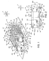
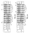
- FIGS 1 through 12 depict an embodiment of a co-planar connector system 10.
- the figures are referenced to a common coordinate system 11 depicted therein.
- the connector system 10 comprises a header connector 12, and a receptacle connector 14 that mates with the header connector 12.
- the header connector 12 can be mounted on a substrate such as a printed circuit board (PCB) 16, and the receptacle connector 14 can be mounted on a substrate such as a PCB 18.
- PCB printed circuit board
- the header connector 12 comprises an electrically insulative housing 22, and a plurality of power contacts 24 mounted in the housing 22.
- Each power contact 24 comprises a first half 26 and a second half 28, as shown in Figure 11 .
- the first half 26 includes a plate-like body member 30a, and a substantially S-shaped portion 31 that adjoins a lower end of the body member 30a.
- the first half 26 also includes a plurality of terminal pins 32 that each extend from a lower end of the S-shaped portion 31.
- the first half 26 further includes three angled contact beams 34a and two substantially straight contact beams 36a that each extend from a forward edge of the body member 30a.
- the angled contact beams 34a and the straight contact beams 36a are arranged on the body member 30a in a staggered manner, i.e., each straight contact beam 36a is positioned adjacent to two of the angled contact beams 34a.
- the second half 28 of each power contact 24 includes a plate-like body member 30b, and another S-shaped portion 31 that adjoins a lower end of the body member 30b.
- the second half 28 also includes a plurality of terminal pins 32 that each extend from a lower end of the S-shaped portion 31.
- the second half 28 further includes three angled contact beams 34b and two substantially straight contact beams 36b that each extend from a forward edge of the body member 30b.
- the angled contact beams 34b and the straight contact beams 36b are arranged on the body member 30b in a staggered manner, as shown in Figure 11 .
- each angled contact beam 34a faces, and is spaced apart from an associated angled contact beam 34b; and each straight contact beam 36a faces and abuts an associated contact beam 36b.
- the S-shaped portions 31 provide an offset between the terminal pins 32 of the first half 26 and the terminal pins 32 of the second half 28 when the body members 30a, 30b are stacked.
- Each body member 30a, 30b can include a tab 42 located at an upper rearward corner thereof.
- the tabs 42 are angled outward, as depicted in Figure 11 .
- Each tab 42 can contact an associated lip (not shown) on the housing 22 as the power contact 24 is inserted into the housing 22 from the rearward end thereof. Contact between the tab 42 and the lip causes the tab 42 to deflect inward. The tab 42 clears the lip as the power contact 24 approaches its fully-inserted position within the housing 22. The resilience of the tab 42 causes the tab 42 to spring outward, to its original position, once the tab 42 clears the lip. Interference between the tab 42 and the lip can discourage the power contact 24 from backing out of the housing 22.
- the housing 22 includes a main body 43 and an adjoining mating portion 44, as shown in Figures 1 through 4 .
- the main body 43 has a plurality of cavities 45 formed therein, as shown in Figures 1 and 3 .
- Each cavity 45 receives the body members 30a, 30b of an associated power contact 24.
- the cavities 45 are each defined, in part, by ribs 46 of the housing 22.
- the ribs 46 are arranged in opposing pairs.
- the ribs 46 contact the body members 30a or 30b of the associated power contact 24 as the power contact 24 is slid into the cavity 45. Interference between the ribs 46 and the body members 30a, 30b pushes the body members 30a, 30b together, and helps to retain the power contact 24 in the cavity 45.
- the ribs 46 define grooves 48 therebetween, as depicted in Figures 1 and 3 .
- the grooves 48 facilitate heat transfer from the power contacts 24 during operation of the header connector 12.
- the main body 43 of the housing 22 includes a forward wall 52.
- the forward wall 52 is depicted, in part, in Figure 4 .
- the cavities 45 extend through the forward wall 52, so that the angled contact beams 34a, 34b and the straight contact beams 36a, 36b of the power contacts 24 can pass through the forward wall 52 when the power contacts 24 are inserted into the housing 22 from the rearward end thereof.
- the mating portion 44 of the housing 22 includes a top portion 56, a bottom portion 58, and side portions 60, 62, as shown in Figures 1-4 and 9 .
- the top portion 56, bottom portion 58, side portions 60, 62, and forward wall 52 define a mating zone or cavity 64, as depicted in Figure 4 .
- the cavity 64 adjoins the cavities 45 of the main body 43.
- the mating portion 44 overhangs a forward edge of the PCB 16 when the header connector 12 is mounted thereon, as shown in Figures 1 through 4 and 9 .
- the angled contact beams 34a, 34b and the straight contact beams 36a, 36b of the power contact 24 extend into the cavity 64, as depicted in Figure 4 .
- the cavity 64 as discussed below, receives a portion of the receptacle connector 14 when the header and receptacle connectors 12, 14 are mated.
- the header connector 12 can include an array 68 of signal contacts 70.
- the array 68 can be located to one side of the power contacts 24, as shown in Figure 4 .
- a portion of the array 70 can be positioned in a cavity 71 formed in the housing 22, as shown in Figure 3 .
- the array 70 can be located at or near the center of the header connector 12, between the power contacts 24, in alternative embodiments of the header connector 12. Other alternative embodiments can forgo the use of any signal contacts 70.
- the main body 43 of the housing 22 has a top portion 75, a bottom portion 76, and side portions 77, 78, as shown in Figures 1-4 .
- a plurality of elorigated slots or apertures 80 are preferably formed in the top portion 75, as shown in Figures 1 , 3 , 4 , 5, and 7 .
- Each aperture 80 is located above the body portions 30a, 30b of the associated power contacts 24.
- the apertures 80 extend in the widthwise, or "z" direction of the housing 22.
- each aperture 80 each adjoin an associated cavity 45, and thereby place the cavity 45 in fluid communication with the environment around the header connector 12.
- the width, or "x" dimension of each aperture 80 is as large as, or greater than the combined width, or "x" dimension, of the body portions 30a, 30b of the associated power contact 24.
- Additional apertures 82 are preferably formed in the top portion 75 of the main body 43, proximate the rearward end thereof, as shown in Figures 1 , 3 , 4 , 5, and 7 .
- Each aperture 82 adjoins an associated cavity 45 and is located above the tabs 42 of the associated power contact 24, as shown in Figures 5 and 7 .
- the apertures 82 place the rearward ends of the cavities 45 in fluid communication with the environment around the header connector 12.
- the width, or "x" dimension of each aperture 82 is about equal to, or greater than the tip-to-tip width of the tabs 42 of the associated power contact 24.
- Apertures 84 are preferably formed in the top portion 56 of the mating portion 44, as shown in Figures 1 and 3-8 .
- the apertures 84 adjoin the cavity 64.
- Each aperture 84 is located above the angled contact beams 34a, 34b and the straight contact beams 36a, 36b of an associated power contact 24, i.e., each aperture 84 is aligned with the angled contact beams 34a, 34b and the straight contact beams 36a, 36b of the associated power contact 24 in the "y" direction, as shown in Figures 6 and 8 .
- each aperture 84 place the cavity 64 fluid communication with the environment around the header connector 12.
- the width, or "x" dimension of each aperture 84 is as large as, or greater than the combined width of the straight contact beams 36a, 36b of the associated power contact 24, as shown in Figures 6 and 8 .
- Apertures 86 are preferably formed in the bottom portion 58 of the mating portion 44, as shown in Figures 9 and 10 .
- the apertures 86 adjoin the cavity 64, and are substantially similar to the apertures 84.
- Each aperture 86 is located below the angled contact beams 34a, 34b and the straight contact beams 36a, 36b of the associated power contact 24, i.e., each aperture 86 is aligned with the angled contact beams 34a, 34b and the straight contact beams 36a, 36b of the associated power contact 24 in the "y" direction, as shown in Figure 10 .
- the apertures 86 place the cavity 64 fluid communication with the environment around the header connector 12.
- a recess 92 is preferably formed in the bottom portion 76 of the main body 43 of the housing 22, as shown in Figures 1 and 2 .
- the recess 92 extends substantially in the lengthwise, or "x" direction of the housing 22, between the side portion 78 and the cavity 71.
- Another recess 94 is preferably formed in the bottom portion 76, between the side portion 77 and the cavity 71, as shown in Figures 3 and 4 .
- the recess 94 substantially aligns with the recess 92 in the "x" direction.
- the recesses 92, 94 each face the PCB 16 when the header connector 12 is mounted thereon.
- the recesses 92, 94, the cavity 71, and the PCB 16 define a passage 98 that extends across the entire length, or "x" dimension of the housing 22.
- the receptacle connector 14 comprises an electrically insulative housing 122, and a plurality of power contacts 124 mounted in the housing 122.
- the power contacts 124 are configured to mate with the power contacts 24 of the header connector 12.
- Each power contact 124 includes a first half 126 and a second half 128, as shown in Figure 12 .
- the power contacts 124 are substantially identical to the power contacts 24, with the exception that the first and second halves 126, 128 each include two of the angled contact beams 34a and three of the substantially straight contact beams 36a. Portions of the power contacts 124 that are substantially identical to those of the power contacts 24 are denoted in the figures by identical reference numerals.
- the angled contact beams 34a and the straight contact beams 36a of the first half 126 are arranged on the body member 30a of the first half 126 in a staggered manner, i.e., each angled contact beam 36a is positioned adjacent to two of the straight contact beams 34a, as shown in Figure 12 .
- the angled contact beams 34b and the straight contact beams 36b likewise are arranged on the body member 30b of the second half 128 in a staggered manner.
- the housing 122 of the receptacle connector 14 includes a main body 143 and an adjoining mating portion 144, as shown in Figures 3 and 4 .
- the mating portion 144 is received within the cavity 64 of the header connector 12 when the header and receptacle connectors 12, 14 are mated.
- the housing 122 has a plurality of cavities 145 formed therein, as shown in Figure 4 .
- the cavities 145 each extend through the main body 143 and the mating portion 144, between the forward and rearward ends the housing 122.
- Each cavity 145 receives the body members 30a, 30b, the angled contact beams 34a, 34b, and the straight contact beams 36a, 36b of an associated power contact 124.
- the angled contact beams 34a, 34b, and the straight contact beams 36a, 36b of each power contact 124 reside within the mating portion 144 when the power contact 124 is inserted in the housing 122.
- Each cavity 145 is defined, in part, by ribs 146 of the housing 122.
- the ribs 146 are arranged in opposing pairs, as shown in Figure 4 .
- the ribs 146 contact the body members 30a or 30b of the associated power contact 124 as the power contact 124 is slid into the cavity 145. Interference between the ribs 146 and the body members 30a, 30b pushes the body members 30a, 30b together, and helps to retain the power contact 124 in the cavity 145.
- the ribs 146 define grooves 148 therebetween.
- the grooves 148 facilitate heat transfer from the power contacts 124 during operation of the receptacle connector 14.
- the receptacle connector 14 can include an array 168 of signal contacts 170, as shown in Figure 3 .
- the array 168 can be located to one side of the power contacts 124, as shown in Figure 3 .
- a portion of the array 168 can be positioned in a cavity 171 formed in the housing 122, as shown in Figure 4 .
- the array 168 can be located at or near the center of the receptacle connector 14, between the power contacts 124, in alternative embodiments of the receptacle connector 14. Other alternative embodiments can forgo the use of any signal contacts 170.
- the main body 143 of the housing 122 has a top portion 175, a bottom portion 176, and side portions 177, 178, as shown in Figures 1-4 .
- a plurality of elongated slots or apertures 180 are preferably formed in the top portion 175, as shown in Figures 1 , 3 , 4 , 5, and 7 .
- Each aperture 180 is located above the body portions 30a, 30b of the associated power contacts 124.
- the apertures 180 extend in the widthwise, or "z" direction of the housing 124.
- the apertures 180 each adjoin an associated cavity 145, and thereby place the cavity 145 in fluid communication with the environment around the receptacle connector 14.
- the width, or "x" dimension of each aperture 180 is as large as, or greater than the combined width, or "x" dimension, of the body portions 30a, 30b of the associated power contact 124.
- Additional apertures 182 are preferably formed in the top portion 175 of the main body 143, proximate the rearward end thereof. Each aperture 182 adjoins an associated cavity 145 and is located above the tabs 42 of the associated power contact 124, as shown in Figures 5 and 7 . The apertures 182 place the rearward ends of the cavities 145 in fluid communication with the environment around the receptacle connector 14. The width, or "x" dimension of each aperture 182 is preferably about equal to, or greater than the tip-to-tip width of the tabs 42 of the associated power contact 124, as shown in Figures 5 and 7 .
- the mating portion 144 of the housing 122 overhangs a forward edge of the PCB 18 when the receptacle connector 14 is mounted thereon, as shown in Figures 3 and 4 .
- the mating portion 144 has a top portion 156 and a bottom portion (not shown).
- Apertures 184 are preferably formed in the top portion 156, as shown in Figures 3-8 .
- the apertures 184 each adjoin the forward end of an associated cavity 145.
- Each aperture 184 is located above the angled contact beams 34a, 34b and the straight contact beams 36a, 36b of an associated power contact 124, i.e., each aperture 84 is aligned with the angled contact beams 34a, 34b and the straight contact beams 36a, 36b of the associated power contact 124 in the "y" direction, as shown in Figures 5 and 6 .
- each aperture 184 place the associated cavity 145 in fluid communication with the environment around the receptacle connector 14.
- the width, or "x" dimension of each aperture 184 is as large as, or greater than the combined width of the straight contact beams 36a, 36b of the associated power contact 124, as shown in Figure 6 .
- Apertures 186 are preferably formed in the bottom portion of the mating portion 144, as shown in Figure 10 .
- the apertures 186 each adjoin the forward end of an associated cavity 145, and are substantially similar to the apertures 184.
- Each aperture 186 is located below the angled contact beams 34a, 34b and the straight contact beams 36a, 36b of the associated power contact 124, i.e., each aperture 186 is aligned with the angled contact beams 34a, 34b and the straight contact beams 36a, 36b of the associated power contact 124 in the "y" direction, as shown in Figure 10 .
- Each aperture 186 places the associated cavity 145 in fluid communication with the environment around the receptacle connector 14.
- a recess 192 is preferably formed in the bottom portion 176 of the main body 143 of the housing 122, as shown in Figures 3 and 4 .
- the recess 192 extends substantially in the lengthwise, or "x" direction of the housing 122, between the side portion 178 and the cavity 171.
- Another recess 194 is preferably formed in the bottom portion 176, between the side portion 177 and the cavity 171, as shown in Figures 1 and 2 .
- the recess 194 substantially aligns with the recess 192 in the "x" direction.
- the recesses 192, 194 each face the PCB 18 when the receptacle connector 14 is mounted thereon.
- the recesses 192, 194, the cavity 171, and the PCB 18 define a passage 198 that extends across the entire length, or "x" dimension of the housing 122.
- the plug and receptacle connectors 12, 14 are mated by aligning the mating portion 144 of the receptacle connector 14 with the cavity 64 of the plug connector 12. One or both of the plug and receptacle connectors 12, 14 are then moved toward each other, until the mating portion 144 begins to enter the cavity 64. Further movement of the plug and receptacle connectors 12, 14 toward each other causes each of the angled contact beams 34a, 34b and the straight contact beams 36a, 36b of the power contacts 24 of the plug connector 12 to enter an associated cavity 145 of the housing 122 of the receptacle connector 14.
- Each associated pair of straight contact beams 36a, 36b of the power contact 24 subsequently enters the space between an associated pair of the angled contact beams 34a, 34b of the power contact 124, as shown in Figures 5 and 6 .
- Contact between the straight contact beams 36a, 36b and the angled contact beams 34a, 34b causes the angled contact beams 36a, 36b to resiliently deflect in an outward direction, i.e., in a direction away from the straight contact beams 34a, 34b.
- the resilient deflection of the angled contact beams 34a, 34b of the power contact 124 results in a contact force between the angled contact beams 34a, 34b of the power contact 124 and the straight contact beams 36a, 36b of the power contact 24.
- Each associated pair of straight contact beams 36a, 36b of the power contact 124 likewise enters the space between an associated pair of the angled contact beams 34a, 34b of the power contact 24.
- the resulting deflection of the angled contact beams 34a, 34b of the power contact 24 results in a contact force between the angled contact beams 34a, 34b of the power contact 124 and the straight contact beams 36a, 36b of the power contact 124.
- the forward edges of the PCB 16 and the PCB 18 are spaced apart by a gap when the plug and receptacle connectors 12, 14 are fully mated. This gap is denoted by the reference character "d" in Figures 1, 2 , and 9 .
- the apertures 84 of the housing 22 and the apertures 184 of the housing 122 are positioned so that each aperture 84 overlaps, or substantially aligns with corresponding aperture 184 when the header and receptacle connectors 12, 14 are fully mated, as shown in Figure 8 .
- the apertures 86 of the housing 22 and the apertures 186 of the housing 122 likewise are positioned so that each aperture 86 overlaps, or substantially aligns with corresponding aperture 186 when the header and receptacle connectors 12, 14 are fully mated, as shown in Figure 10 .
- the apertures 84, 86, 184, 186 facilitate air circulation through the housings 22, 122 and over the power contacts 24, 124. This air circulation can help to cool the power contacts 24, 124 during operation.
- Figures 1 and 2 include arrows 200 designating one possible manner in which air can circulate through the header and receptacle connectors 12, 14.
- one or more cooling fans (not shown) are used to direct air downward and over the header and receptacle connectors 12, 14.
- the overlapping apertures 84, 184 permit the relatively cool, downwardly-flowing air to enter the mating portions 44, 144 of the respective housings 22, 122.
- the air entering the mating portions 44, 144 can displace the air within the mating portions 44, 144, which has been heated by the angled contact beams 34a, 34a and the straight contact beams 36a, 36b of the relatively warm power contacts 24, 124.
- the lower apertures 86, 186 can permit the heated air that has been displaced,within the mating portions 44, 144 by the cooler incoming air to exit the mating portions 44, 144.
- the gap "d" between the PCBs 16, 18 permits the air exiting the mating portions 44, 144 to flow freely into the environment around the header and receptacle connectors 12, 14.
- Heat energy is transferred to the relatively cool air from the angled contact beams 34a, 34b and the straight contact beams 36a, 36b, as the air is forced downward and over the angled contact beams 34a, 34b and the straight contact beams 36a, 36b.
- This convective heat transfer cools the angled contact beams 34a, 34b and the straight contact beams 36a, 36b, while heating the air.
- the heated air in turn, is forced downward and through the overlapping lower apertures 86, 186, giving rise to an air-circulation pattern within the mating portions 44, 144.
- This circulation dissipates heat energy from the power contacts 24, 124, and thereby cools the power contacts 24, 124.
- the apertures 80, 180 also facilitate cooling of the respective power contacts 24, 124 during operation.
- the apertures 80, 180 permit the relatively cool air being forced downward over the header and receptacle connectors 12, 14 to impinge upon the top of each body portion 30a, 30b of the power contacts 24, 124.
- the impingement of the relatively cool air on the body portions 30a, 30b helps to dissipate heat energy from the power contacts 24, 124.
- the apertures 82, 182 likewise facilitate cooling of the respective power contacts 24, 124.
- the apertures 82, 182 permit the relatively cool air being forced downward over the header and receptacle connectors 12, 14 to impinge upon the top of each tab 42 of the power contacts 24, 124. The impingement of the relatively cool air on the tabs 42 helps to dissipate heat energy from the power contacts 24,124.
- the grooves 48, 148 of the respective housings 22, 122 are configured so that each groove 48 substantially aligns with an associated groove 148 when the header and receptacle connectors 12, 24 are mated.
- This arrangement can facilitate cooling of the power contacts 24, 124. For example, relatively cool air can be forced over the header and receptacle connectors 12, 14 in the "z" direction, as denoted in Figures 1 and 2 , by one or more additional cooling fans. The cooling air can enter the rearward ends of the grooves 48.
- the cooling air can travel the entire combined width, or "z" dimension, of the header and receptacle connectors 12, 14, and can exit the housing 22 by way of the distal ends of the grooves 148.
- the cool air being forced through the grooves 48, 148 passes over the relatively warm body portions 30a, 30b of the power contacts 24, 124.
- the air dissipates heat energy from the body portions 30a, 30b through convective heat transfer, and thereby cools the power contacts 24, 124.
- the recesses 92, 94 and the cavity 71 formed in the housing 22, and the PCB 16 define a passage 98, as discussed above.
- the passage 98 can facilitate cooling of the power contacts 24.
- relatively cool air can be forced into and through the passage 98 in the "x" direction, as denoted in Figure 1 , by one or more additional cooling fans.
- the S-shaped portions 31 and the adjoining terminal pins 32 of the power contacts 24 are partially located within the passage 98, as shown in Figure 2 .
- the air flowing through the passage 98 can flow over and under the S-shaped portions 31, and between the terminal pins 31.
- the relatively cool air dissipates heat energy from the power contacts 24 through convective heat transfer, thereby cooling the power contacts 24.
- the recesses 192, 194 and the cavity 171 formed in the housing 122, and the PCB 18 define a passage 198, as discussed above.
- the passage 198 can facilitate cooling of the power contacts 124 of the receptacle connector 14, in the manner discussed above in relation to the passage 98.
- the above described air-circulation features of the header and receptacle contacts 12, 14 facilitate three-dimensional circulation of cooling air within the header and receptacle contacts 12, 14.
- the cooling of the power contacts 24, 124 facilitated by these features can permit the power contacts 24, 124 to operate at higher currents than would otherwise be possible.
- the maximum current rating of power contacts 24, 124 may be limited by the maximum acceptable temperature rise in the power contacts 24, 124.
- the heat dissipation facilitated by some or all of the above-described air-circulation features can permit the power contacts 24, 124 to operate at a higher current, with the same temperature rise as experienced in an application where the power contacts 24, 124 are not cooled.
- the maximum rated current of the power contacts 24, 124 can be increased without substantially increasing the temperature rise therein.
- the above-described airflow patterns, and the airflow patterns denoted in the figures are presented for illustrative purposes only.
- the airflow patterns through and around the header and receptacle connectors 12, 14 can be more complex that the patterns described and illustrated herein.
- the airflow patterns can change when the orientations of the header and receptacle connectors 12, 14 are different than those denoted in the figures.
- header and receptacle connectors 12, 14 can be operated without forced-air cooling; heat dissipation in this type of application can be achieved primarily through natural convection.
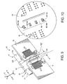
- Figures 13 and 14 depict an alternative embodiment in the form of a connector system 210.
- the connector system 210 is configured for use as a backplane connector system.
- the connector system 210 can include the header connector 12 described above in relation to the connector system 10.
- the connector system 210 can also include a vertical receptacle connector 212 that mates with the header connector 12.
- the header connector 12 can be mounted on a daughter card 213.
- the receptacle connector 212 can be mounted on a motherboard 214 that is oriented substantially perpendicular to the daughter card 213.
- the receptacle connector 212 can have features substantially similar or identical to those described above in relation to the receptacle connector 14 for facilitating air circulation through and around the receptacle connector 212.
- the receptacle connector 212 can have a housing 216 with a mating portion (not shown) that is received by the mating portion 43 of the header connector 12 when the header and receptacle connectors 12, 212 are mated.
- the mating portion of the housing 216 can have apertures formed in top and bottom potions thereof. The apertures can align with the apertures 84, 184 formed in the mating portion 44 of the header connector 12.
- the housing 216 of the receptacle connector 212 can have one or more recesses 218 formed therein.
- the recesses 218 and the motherboard 214 can define a passage.220 that facilitates air circulation between the housing 216 and the motherboard 214, in the manner discussed above in relation to the passage 198 defined by the receptacle connector 14 and the PCB 18.
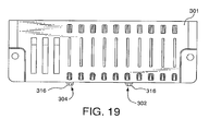
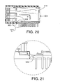
- FIGS 15-21 depict an alternative embodiment of the header connector 12 in the form of a header connector 300.
- the header connector 300 can be substantially similar or identical to the header connector 12.
- the header connector 300 includes a housing 301, short power contacts 302, and long power contacts 304.
- the short power contacts 302 are received in cavities 306 formed in the housing 301.
- the long power contacts 304 are received in cavities 308 formed in the housing 301.
- each cavity 306, 308 has a window 312 formed therein.
- the window 312 associated with each cavity 306 is located proximate a lower end of the cavity 306, as shown in Figures 15 , 17, and 18 .
- the window 312 associated with each cavity 308 is located proximate an upper end of the cavity 306.
- the short and long power contacts 302, 304 each include body members 314a, 314b, as shown in Figures 16A and 16B .
- the short and long power contacts 302, 304 also include tabs 316 located proximate the rearward edges of each body member 314a, 314b.
- the tabs 316 extend in directions substantially perpendicular to the major surfaces of the body members 314a, 314b.
- the tabs 316 of each short power contact 302 are located proximate a lower end of the short power contact 302.
- the tabs 316 of each long power contact 304 are located proximate an upper end of the long power contact 304.
- the tabs 316 are sized to fit within the windows 312 of the housing 301.
- the windows 312 associated with the cavities 306, and the tabs 316 of each short power contact 302 are positioned so that the tabs 316 of the short power contacts 302 each align with, and are received by an associated one of the windows 312 of the cavities 306 when the short power contacts 302 are inserted into the cavities 306, as shown in Figure 17 .
- the tabs 316 of the short power contacts 302 do not align with the windows 312 associated with the cavities 308 when an attempt is made to insert one of the short power contacts 302 into one of the cavities 308. Rather, interference between the tabs 316 and the housing 301 prevents the short power contact 302 from advancing into the cavity 308, as shown in Figures 18 and 19 .
- the windows 312 associated with the cavities 308, and the tabs 316 of each long power contact 304 likewise are positioned so that the tabs 316 of the long power contacts 304 align with, and are received by the windows 312 of the cavities 308 when the long power contacts 304 are inserted into the cavities 308, as shown in Figure 17 .
- the tabs 316 of the long power contacts 304 do not align with the windows 312 associated with the cavities 306 when an attempt is made to insert one of the long power contacts 304 into one of the cavities 306. Rather, interference between the tabs 316 and the housing 301 prevents the long power contact 304 from advancing into the cavity 306, as shown in Figures 18 and 19 .
- the body members 314a, 314b of the short and long power contacts 302, 304 each include a tab 328, as shown in Figures 16A, 16B , 20, and 21 .
- the tabs 328 interferedly engage the housing 301 when the short and long power contacts 302, 304 are fully inserted into the housing 301. Interference between the tabs 328 and the housing 301 helps to retain the short and long power contacts 302, 304 in the housing 301.
- the housing 301 includes a ramp 303 that helps to guide the tabs 328 into their final positions as the body members 314a, 314b are inserted into the housing 301.
- the above-noted noted interference between the tabs 316 of the long power contacts 304 and the housing 301 when the long power contacts 304 are inadvertently installed in the cavities 306 can prevent the long power contacts 304 from advancing far enough into the cavities 306 for the associated tabs 328 to interferedly engage the associated ramps 303 of the housing 301.
- the above-noted noted interference between the tabs 316 of the short power contacts 302 and the housing 301 when the short power contacts 302 are inadvertently installed in the cavities 308 can likewise prevent the short power contacts 302 from advancing far enough into the cavities 308 for the associated tabs 328 to interferedly engage in the associated ramps 303.
- the second half 314b of each short and long power contact 302, 304 can include two cylindrical projections 350, as shown in Figures 16A and 16B .
- the first half 314a of each short and long power contact 302, 304 can include two circular holes 352 that each receive one of the projections 350.
- the relative positions of the two sets of projections 350 and holes 352 on the short power contacts 302 can differ from the relative locations of the two sets of projections 350 and holes 352 on the long power contacts 304.
- the projections 350 and holes 352 can thus act as polarizing features that prevent the first half of a short power contact 302 from being inadvertently mated with the second half of a long power contact 304, and vice versa.
- the projections 350 and holes 352 can have respective shapes other than cylindrical and circular in alternative embodiments. Moreover, the projections 350 and the holes 352 can be located on the first and second halves 323a, 323b, respectively, of the short and long power contacts 302, 304 in alternative embodiments.
- Figures 22A through 24 depict alternative embodiments of the short and long power contacts 302, 304 in the form of a short power contact 320 and a long power contact 322.
- the short and long power contacts 320, 322 are substantially similar to the respective short and long power contacts 302, 304 from a structural and functional perspective, with the exception that the short and long power contacts 320, 322 include tabs 324 that angle outwardly and downwardly from the associated body members 323a, 323b of the short and long power contacts 320, 322.
Abstract
Description
- The present invention relates to electrical connectors for transmitting electrical power.
- Increasing the operating current of an electronic device, in general, permits the device to operate at a lower voltage than would otherwise be possible. Manufacturers of electronic devices therefore often request or require power contacts with relatively high current ratings. Consequently, it is desirable to minimize the temperature rise experienced by power contacts during operation.
- Assembling contacts into a connector housing can also be problematic. Contacts can be inserted into improper cavities or only partially inserted into a cavity.
- Embodiments of electrical connectors include features that facilitate circulation of air through and around the electrical connectors. The air can cool the power contacts of the electrical connectors, thereby allowing the power contacts to operate at higher currents that would otherwise be possible. Features are also included to help prevent mis-insertion or partial insertion of contacts into a housing.
- Embodiments of connector systems comprise a first electrical connector comprising an electrically-insulative housing that defines a cavity. The housing has an aperture formed therein that places the cavity in fluid communication with the environment around the first electrical connector. The first electrical connector also comprises a power contact having a mating portion located in the cavity.
- The connector system also comprises a second electrical connector that mates with the first electrical connector. The second electrical connector comprises an electrically-insulative housing that defines a cavity. The housing of the second electrical connector has an aperture formed therein that places the cavity of the second electrical connector in fluid communication with the environment around the second electrical connector. The second electrical connector also comprises a power contact having a mating portion located in the cavity of the housing of the second electrical connector.
- The apertures formed in the housings of the first and second electrical connectors overlap when the first and second electrical connectors are mated.
- Embodiments of electrical connectors for mounting on a substrate comprise a power contact and an electrically insulative housing that receives the power contact. An aperture is formed in the housing. The aperture is aligned with a mating portion of power contact whereby air heated by the power contact can exit the power contact by way of the aperture. A recess is formed in the housing. The recess faces the substrate, and the recess and the substrate define a passage extending from a side portion of the housing when the electrical connector is mounted on the substrate. A portion of the power contact extends through the recess, whereby air from the environment around the electrical connector can pass between the housing and substrate and over the power contact.
- Embodiments of electrical connectors comprise an electrically insulative housing, and a power contact mounted in the housing and having a mating portion. The housing has an aperture formed therein and aligned with the mating portion of the contact whereby air heated by the power contact can exit the power contact by way of the aperture.
- Embodiments of electrical connectors include a housing and two different types of power contacts. The power contacts include polarizing features that reduce or eliminate the potential for the power contacts to be improperly installed in the housing.
- Embodiments of electrical connectors comprise a first power contact comprising a tab; a second power contact comprising a tab; and a housing having a first and a second cavity formed therein that receive the respective first and second power contacts. The tab of the first power contact interferedly contacts the housing when the first power contact is partially inserted into the second cavity thereby preventing installation of the first power contact in the second cavity. The tab of the second power contact interferedly contacts the housing when the second power contact is partially inserted into the first cavity thereby preventing installation of the second power contact in the first cavity.
- The foregoing summary, as well as the following detailed description of a preferred embodiment, are better understood when read in conjunction with the appended diagrammatic drawings. For the purpose of illustrating the invention, the drawings show an embodiment that is presently preferred. The invention is not limited, however, to the specific instrumentalities disclosed in the drawings. In the drawings:
-
Figure 1 is a top perspective view of a preferred embodiment of a connector system depicting a header connector and a receptacle connector of the connector system in a fully mated condition; -
Figure 2 is a side view of the connector system shown inFigure 1 , depicting the header connector and the receptacle connector in the fully mated condition; -
Figure 3 is a top perspective view of the connector system shown inFigures 1 and 2 , depicting the header connector and the receptacle connector an unmated condition; -
Figure 4 is a top perspective view of the connector system shown inFigures 1-3 , depicting the header connector and the receptacle connector the unmated condition; -
Figure 5 is top view of the connector system shown inFigures 1-4 , depicting the header connector and the receptacle connector in a partially mated condition; -
Figure 6 is a magnified, partial cutaway view of the area designated "A" inFigure 5 ; -
Figure 7 is top view of the connector system shown inFigures 1-6 , depicting the header connector and the receptacle connector in the fully mated condition; -
Figure 8 is a magnified, partial cutaway view of the area designated "B" inFigure 7 ; -
Figure 9 is bottom perspective view of the connector system shown inFigures 1-8 , depicting the header connector and the receptacle connector in the fully mated condition; -
Figure 10 is a magnified view of the area designated "C" inFigure 9 ; -
Figures 11 and 12 are perspective views of a power contact of the header connector shown inFigures 1-10 ; -
Figure 13 is a top perspective view of an alternative embodiment of the connector system shown inFigures 1-12 , depicting a header connector and a receptacle connector of the connector system in a fully mated condition; -
Figure 14 is a bottom perspective view of the connector system shown inFigure 13 , depicting the header connector and the receptacle connector in the fully mated condition -
Figure 15 is a rear perspective view of a housing of another alternative embodiment of the connector system shown inFigures 1-12 ; -
Figures 16A and 16B are rear perspective views of a respective long and short power contact of the connector system shown inFigure 15 ; -
Figure 17 is rear view of the connector system shown inFigures 15-16B , depicting the short and long power contacts correctly installed in associated cavities in the housing; -
Figure 18 is a rear view of the connector system shown inFigures 15-17 , depicting one of the short and one of the long power contacts incorrectly correctly installed in associated cavities in the housing; -
Figure 19 is a top view of the connector system shown inFigures 15-18 , depicting one of the short and one of the long power contacts incorrectly correctly installed in associated cavities in the housing; -
Figure 20 is a cross-sectional view of the connector system shown inFigures 15-19 , taken through the line "D-D" ofFigure 17 ; -
Figure 21 is a magnified view of the area designated "E" inFigure 20 ; -
Figures 22A and 22B are perspective views of a respective long and short power contact of another alternative embodiment of the connector system shown inFigures 1-12 ; -
Figure 23 a rear view of the connector system shown inFigures 15-16B , depicting the short and long power contacts correctly installed in associated cavities in a housing of the connector system; and -
Figure 24 is a rear view of the connector system shown inFigures 22A-23 , depicting one of the short and one of the long power contacts incorrectly correctly installed in associated cavities in the housing. -
Figures 1 through 12 depict an embodiment of aco-planar connector system 10. The figures are referenced to acommon coordinate system 11 depicted therein. Theconnector system 10 comprises aheader connector 12, and areceptacle connector 14 that mates with theheader connector 12. Theheader connector 12 can be mounted on a substrate such as a printed circuit board (PCB) 16, and thereceptacle connector 14 can be mounted on a substrate such as aPCB 18. Theheader connector 12 and thereceptacle connector 14, when mated, electrically connect thePCB 16 and thePCB 18. - The
header connector 12 comprises an electricallyinsulative housing 22, and a plurality ofpower contacts 24 mounted in thehousing 22. Eachpower contact 24 comprises afirst half 26 and asecond half 28, as shown inFigure 11 . Thefirst half 26 includes a plate-like body member 30a, and a substantially S-shapedportion 31 that adjoins a lower end of thebody member 30a. Thefirst half 26 also includes a plurality ofterminal pins 32 that each extend from a lower end of the S-shapedportion 31. - The
first half 26 further includes threeangled contact beams 34a and two substantiallystraight contact beams 36a that each extend from a forward edge of thebody member 30a. Theangled contact beams 34a and thestraight contact beams 36a are arranged on thebody member 30a in a staggered manner, i.e., eachstraight contact beam 36a is positioned adjacent to two of theangled contact beams 34a. - Directional terms such as "upper," "lower," "forward," "rearward," "top," "bottom," "above," "below," etc., are used with reference to the component orientations depicted in
Figure 1 . These terms are used for exemplary purposes only, and are not intended to limit the scope of the appended claims. - The
second half 28 of eachpower contact 24 includes a plate-like body member 30b, and another S-shapedportion 31 that adjoins a lower end of thebody member 30b. Thesecond half 28 also includes a plurality ofterminal pins 32 that each extend from a lower end of the S-shapedportion 31. - The
second half 28 further includes three angled contact beams 34b and two substantiallystraight contact beams 36b that each extend from a forward edge of thebody member 30b. The angled contact beams 34b and thestraight contact beams 36b are arranged on thebody member 30b in a staggered manner, as shown inFigure 11 . - The
body members Figure 11 , so that eachangled contact beam 34a faces, and is spaced apart from an associatedangled contact beam 34b; and eachstraight contact beam 36a faces and abuts an associatedcontact beam 36b. The S-shapedportions 31 provide an offset between theterminal pins 32 of thefirst half 26 and the terminal pins 32 of thesecond half 28 when thebody members - Each
body member tab 42 located at an upper rearward corner thereof. Thetabs 42 are angled outward, as depicted inFigure 11 . Eachtab 42 can contact an associated lip (not shown) on thehousing 22 as thepower contact 24 is inserted into thehousing 22 from the rearward end thereof. Contact between thetab 42 and the lip causes thetab 42 to deflect inward. Thetab 42 clears the lip as thepower contact 24 approaches its fully-inserted position within thehousing 22. The resilience of thetab 42 causes thetab 42 to spring outward, to its original position, once thetab 42 clears the lip. Interference between thetab 42 and the lip can discourage thepower contact 24 from backing out of thehousing 22. - Specific details of the
power contacts 24 are presented for exemplary purposes only. The principles of the present invention can be applied to connectors comprising other types of power contacts, including the power contacts described in the related applications cross-referenced above. - The
housing 22 includes amain body 43 and an adjoiningmating portion 44, as shown inFigures 1 through 4 . Themain body 43 has a plurality ofcavities 45 formed therein, as shown inFigures 1 and3 . Eachcavity 45 receives thebody members power contact 24. Thecavities 45 are each defined, in part, byribs 46 of thehousing 22. Theribs 46 are arranged in opposing pairs. Theribs 46 contact thebody members power contact 24 as thepower contact 24 is slid into thecavity 45. Interference between theribs 46 and thebody members body members power contact 24 in thecavity 45. - The
ribs 46 definegrooves 48 therebetween, as depicted inFigures 1 and3 . Thegrooves 48, as discussed below, facilitate heat transfer from thepower contacts 24 during operation of theheader connector 12. - The
main body 43 of thehousing 22 includes aforward wall 52. Theforward wall 52 is depicted, in part, inFigure 4 . Thecavities 45 extend through theforward wall 52, so that theangled contact beams straight contact beams power contacts 24 can pass through theforward wall 52 when thepower contacts 24 are inserted into thehousing 22 from the rearward end thereof. - The
mating portion 44 of thehousing 22 includes atop portion 56, abottom portion 58, andside portions Figures 1-4 and9 . Thetop portion 56,bottom portion 58,side portions forward wall 52 define a mating zone orcavity 64, as depicted inFigure 4 . Thecavity 64 adjoins thecavities 45 of themain body 43. Themating portion 44 overhangs a forward edge of thePCB 16 when theheader connector 12 is mounted thereon, as shown inFigures 1 through 4 and9 . - The
angled contact beams straight contact beams power contact 24 extend into thecavity 64, as depicted inFigure 4 . Thecavity 64, as discussed below, receives a portion of thereceptacle connector 14 when the header andreceptacle connectors - The
header connector 12 can include anarray 68 ofsignal contacts 70. Thearray 68 can be located to one side of thepower contacts 24, as shown inFigure 4 . A portion of thearray 70 can be positioned in acavity 71 formed in thehousing 22, as shown inFigure 3 . Thearray 70 can be located at or near the center of theheader connector 12, between thepower contacts 24, in alternative embodiments of theheader connector 12. Other alternative embodiments can forgo the use of anysignal contacts 70. - The
main body 43 of thehousing 22 has atop portion 75, a bottom portion 76, andside portions Figures 1-4 . A plurality of elorigated slots orapertures 80 are preferably formed in thetop portion 75, as shown inFigures 1 ,3 ,4 ,5, and 7 . Eachaperture 80 is located above thebody portions power contacts 24. Theapertures 80 extend in the widthwise, or "z" direction of thehousing 22. - The
apertures 80 each adjoin an associatedcavity 45, and thereby place thecavity 45 in fluid communication with the environment around theheader connector 12. Preferably, the width, or "x" dimension of eachaperture 80 is as large as, or greater than the combined width, or "x" dimension, of thebody portions power contact 24. -
Additional apertures 82 are preferably formed in thetop portion 75 of themain body 43, proximate the rearward end thereof, as shown inFigures 1 ,3 ,4 ,5, and 7 . Eachaperture 82 adjoins an associatedcavity 45 and is located above thetabs 42 of the associatedpower contact 24, as shown inFigures 5 and 7 . Theapertures 82 place the rearward ends of thecavities 45 in fluid communication with the environment around theheader connector 12. Preferably, the width, or "x" dimension of eachaperture 82 is about equal to, or greater than the tip-to-tip width of thetabs 42 of the associatedpower contact 24. -
Apertures 84 are preferably formed in thetop portion 56 of themating portion 44, as shown inFigures 1 and3-8 . Theapertures 84 adjoin thecavity 64. Eachaperture 84 is located above theangled contact beams straight contact beams power contact 24, i.e., eachaperture 84 is aligned with theangled contact beams straight contact beams power contact 24 in the "y" direction, as shown inFigures 6 and 8 . - The
apertures 84 place thecavity 64 fluid communication with the environment around theheader connector 12. Preferably the width, or "x" dimension of eachaperture 84 is as large as, or greater than the combined width of thestraight contact beams power contact 24, as shown inFigures 6 and 8 . -
Apertures 86 are preferably formed in thebottom portion 58 of themating portion 44, as shown inFigures 9 and 10 . Theapertures 86 adjoin thecavity 64, and are substantially similar to theapertures 84. Eachaperture 86 is located below theangled contact beams straight contact beams power contact 24, i.e., eachaperture 86 is aligned with theangled contact beams straight contact beams power contact 24 in the "y" direction, as shown inFigure 10 . Theapertures 86 place thecavity 64 fluid communication with the environment around theheader connector 12. - A
recess 92 is preferably formed in the bottom portion 76 of themain body 43 of thehousing 22, as shown inFigures 1 and 2 . Therecess 92 extends substantially in the lengthwise, or "x" direction of thehousing 22, between theside portion 78 and thecavity 71. Anotherrecess 94 is preferably formed in the bottom portion 76, between theside portion 77 and thecavity 71, as shown inFigures 3 and 4 . Therecess 94 substantially aligns with therecess 92 in the "x" direction. - The
recesses PCB 16 when theheader connector 12 is mounted thereon. Therecesses cavity 71, and thePCB 16 define apassage 98 that extends across the entire length, or "x" dimension of thehousing 22. - The
receptacle connector 14 comprises an electricallyinsulative housing 122, and a plurality ofpower contacts 124 mounted in thehousing 122. Thepower contacts 124 are configured to mate with thepower contacts 24 of theheader connector 12. - Each
power contact 124 includes afirst half 126 and asecond half 128, as shown inFigure 12 . Thepower contacts 124 are substantially identical to thepower contacts 24, with the exception that the first andsecond halves angled contact beams 34a and three of the substantiallystraight contact beams 36a. Portions of thepower contacts 124 that are substantially identical to those of thepower contacts 24 are denoted in the figures by identical reference numerals. - The
angled contact beams 34a and thestraight contact beams 36a of thefirst half 126 are arranged on thebody member 30a of thefirst half 126 in a staggered manner, i.e., eachangled contact beam 36a is positioned adjacent to two of thestraight contact beams 34a, as shown inFigure 12 . The angled contact beams 34b and thestraight contact beams 36b likewise are arranged on thebody member 30b of thesecond half 128 in a staggered manner. - The
housing 122 of thereceptacle connector 14 includes amain body 143 and an adjoiningmating portion 144, as shown inFigures 3 and 4 . Themating portion 144, as discussed below, is received within thecavity 64 of theheader connector 12 when the header andreceptacle connectors - The
housing 122 has a plurality ofcavities 145 formed therein, as shown inFigure 4 . Thecavities 145 each extend through themain body 143 and themating portion 144, between the forward and rearward ends thehousing 122. Eachcavity 145 receives thebody members angled contact beams straight contact beams power contact 124. Theangled contact beams straight contact beams power contact 124 reside within themating portion 144 when thepower contact 124 is inserted in thehousing 122. - Each
cavity 145 is defined, in part, byribs 146 of thehousing 122. Theribs 146 are arranged in opposing pairs, as shown inFigure 4 . Theribs 146 contact thebody members power contact 124 as thepower contact 124 is slid into thecavity 145. Interference between theribs 146 and thebody members body members power contact 124 in thecavity 145. - The
ribs 146 definegrooves 148 therebetween. Thegrooves 148, as discussed below, facilitate heat transfer from thepower contacts 124 during operation of thereceptacle connector 14. - The
receptacle connector 14 can include anarray 168 of signal contacts 170, as shown inFigure 3 . Thearray 168 can be located to one side of thepower contacts 124, as shown inFigure 3 . A portion of thearray 168 can be positioned in acavity 171 formed in thehousing 122, as shown inFigure 4 . Thearray 168 can be located at or near the center of thereceptacle connector 14, between thepower contacts 124, in alternative embodiments of thereceptacle connector 14. Other alternative embodiments can forgo the use of any signal contacts 170. - The
main body 143 of thehousing 122 has atop portion 175, a bottom portion 176, andside portions Figures 1-4 . A plurality of elongated slots orapertures 180 are preferably formed in thetop portion 175, as shown inFigures 1 ,3 ,4 ,5, and 7 . Eachaperture 180 is located above thebody portions power contacts 124. Theapertures 180 extend in the widthwise, or "z" direction of thehousing 124. Theapertures 180 each adjoin an associatedcavity 145, and thereby place thecavity 145 in fluid communication with the environment around thereceptacle connector 14. Preferably, the width, or "x" dimension of eachaperture 180 is as large as, or greater than the combined width, or "x" dimension, of thebody portions power contact 124. -
Additional apertures 182 are preferably formed in thetop portion 175 of themain body 143, proximate the rearward end thereof. Eachaperture 182 adjoins an associatedcavity 145 and is located above thetabs 42 of the associatedpower contact 124, as shown inFigures 5 and 7 . Theapertures 182 place the rearward ends of thecavities 145 in fluid communication with the environment around thereceptacle connector 14. The width, or "x" dimension of eachaperture 182 is preferably about equal to, or greater than the tip-to-tip width of thetabs 42 of the associatedpower contact 124, as shown inFigures 5 and 7 . - The
mating portion 144 of thehousing 122 overhangs a forward edge of thePCB 18 when thereceptacle connector 14 is mounted thereon, as shown inFigures 3 and 4 . Themating portion 144 has atop portion 156 and a bottom portion (not shown).Apertures 184 are preferably formed in thetop portion 156, as shown inFigures 3-8 . Theapertures 184 each adjoin the forward end of an associatedcavity 145. Eachaperture 184 is located above theangled contact beams straight contact beams power contact 124, i.e., eachaperture 84 is aligned with theangled contact beams straight contact beams power contact 124 in the "y" direction, as shown inFigures 5 and 6 . - The
apertures 184 place the associatedcavity 145 in fluid communication with the environment around thereceptacle connector 14. Preferably, the width, or "x" dimension of eachaperture 184 is as large as, or greater than the combined width of thestraight contact beams power contact 124, as shown inFigure 6 . - Apertures 186 are preferably formed in the bottom portion of the
mating portion 144, as shown inFigure 10 . The apertures 186 each adjoin the forward end of an associatedcavity 145, and are substantially similar to theapertures 184. Each aperture 186 is located below theangled contact beams straight contact beams power contact 124, i.e., each aperture 186 is aligned with theangled contact beams straight contact beams power contact 124 in the "y" direction, as shown inFigure 10 . Each aperture 186 places the associatedcavity 145 in fluid communication with the environment around thereceptacle connector 14. - A
recess 192 is preferably formed in the bottom portion 176 of themain body 143 of thehousing 122, as shown inFigures 3 and 4 . Therecess 192 extends substantially in the lengthwise, or "x" direction of thehousing 122, between theside portion 178 and thecavity 171. Anotherrecess 194 is preferably formed in the bottom portion 176, between theside portion 177 and thecavity 171, as shown inFigures 1 and 2 . Therecess 194 substantially aligns with therecess 192 in the "x" direction. - The
recesses PCB 18 when thereceptacle connector 14 is mounted thereon. Therecesses cavity 171, and thePCB 18 define apassage 198 that extends across the entire length, or "x" dimension of thehousing 122. - The plug and
receptacle connectors mating portion 144 of thereceptacle connector 14 with thecavity 64 of theplug connector 12. One or both of the plug andreceptacle connectors mating portion 144 begins to enter thecavity 64. Further movement of the plug andreceptacle connectors angled contact beams straight contact beams power contacts 24 of theplug connector 12 to enter an associatedcavity 145 of thehousing 122 of thereceptacle connector 14. - Each associated pair of
straight contact beams power contact 24 subsequently enters the space between an associated pair of theangled contact beams power contact 124, as shown inFigures 5 and 6 . Contact between thestraight contact beams angled contact beams angled contact beams straight contact beams angled contact beams power contact 124 results in a contact force between theangled contact beams power contact 124 and thestraight contact beams power contact 24. - Each associated pair of
straight contact beams power contact 124 likewise enters the space between an associated pair of theangled contact beams power contact 24. The resulting deflection of theangled contact beams power contact 24 results in a contact force between theangled contact beams power contact 124 and thestraight contact beams power contact 124. - The forward edges of the
PCB 16 and thePCB 18 are spaced apart by a gap when the plug andreceptacle connectors Figures 1, 2 , and9 . - The
apertures 84 of thehousing 22 and theapertures 184 of thehousing 122 are positioned so that eachaperture 84 overlaps, or substantially aligns withcorresponding aperture 184 when the header andreceptacle connectors Figure 8 . - The
apertures 86 of thehousing 22 and the apertures 186 of thehousing 122 likewise are positioned so that eachaperture 86 overlaps, or substantially aligns with corresponding aperture 186 when the header andreceptacle connectors Figure 10 . - The
apertures housings power contacts power contacts - For example,
Figures 1 and 2 includearrows 200 designating one possible manner in which air can circulate through the header andreceptacle connectors receptacle connectors apertures mating portions respective housings mating portions mating portions angled contact beams straight contact beams warm power contacts - The
lower apertures 86, 186 can permit the heated air that has been displaced,within themating portions mating portions PCBs mating portions receptacle connectors - Heat energy is transferred to the relatively cool air from the
angled contact beams straight contact beams angled contact beams straight contact beams angled contact beams straight contact beams lower apertures 86, 186, giving rise to an air-circulation pattern within themating portions power contacts power contacts - The
apertures respective power contacts apertures receptacle connectors body portion power contacts body portions power contacts - The
apertures respective power contacts apertures receptacle connectors tab 42 of thepower contacts tabs 42 helps to dissipate heat energy from the power contacts 24,124. - The
grooves respective housings groove 48 substantially aligns with an associatedgroove 148 when the header andreceptacle connectors power contacts receptacle connectors Figures 1 and 2 , by one or more additional cooling fans. The cooling air can enter the rearward ends of thegrooves 48. As eachgroove 48 substantially aligns with acorresponding groove 148 in thehousing 122, the cooling air can travel the entire combined width, or "z" dimension, of the header andreceptacle connectors housing 22 by way of the distal ends of thegrooves 148. - The cool air being forced through the
grooves warm body portions power contacts body portions power contacts - The
recesses cavity 71 formed in thehousing 22, and thePCB 16 define apassage 98, as discussed above. Thepassage 98 can facilitate cooling of thepower contacts 24. In particular, relatively cool air can be forced into and through thepassage 98 in the "x" direction, as denoted inFigure 1 , by one or more additional cooling fans. The S-shapedportions 31 and the adjoining terminal pins 32 of thepower contacts 24 are partially located within thepassage 98, as shown inFigure 2 . The air flowing through thepassage 98 can flow over and under the S-shapedportions 31, and between the terminal pins 31. The relatively cool air dissipates heat energy from thepower contacts 24 through convective heat transfer, thereby cooling thepower contacts 24. - The
recesses cavity 171 formed in thehousing 122, and thePCB 18 define apassage 198, as discussed above. Thepassage 198 can facilitate cooling of thepower contacts 124 of thereceptacle connector 14, in the manner discussed above in relation to thepassage 98. - The above described air-circulation features of the header and
receptacle contacts receptacle contacts power contacts power contacts power contacts power contacts power contacts power contacts power contacts - The above-described airflow patterns, and the airflow patterns denoted in the figures are presented for illustrative purposes only. The airflow patterns through and around the header and
receptacle connectors receptacle connectors - Different airflow patterns can be created by directing the cooling air at the header and
receptacle connectors receptacle connectors - The foregoing description is provided for the purpose of explanation and is not to be construed as limiting the invention. Although the invention has been described with reference to preferred embodiments or preferred methods, it is understood that the words which have been used herein are words of description and illustration, rather than words of limitation. Furthermore, although the invention has been described herein with reference to particular structure, methods, and embodiments, the invention is not intended to be limited to the particulars disclosed herein, as the invention extends to all structures, methods and uses that are within the scope of the appended claims. Those skilled in the relevant art, having the benefit of the teachings of this specification, may effect numerous modifications to the invention as described herein, and changes may be made without departing from the scope and spirit of the invention as defined by the appended claims.
- For example,
Figures 13 and 14 depict an alternative embodiment in the form of aconnector system 210. Theconnector system 210 is configured for use as a backplane connector system. Theconnector system 210 can include theheader connector 12 described above in relation to theconnector system 10. Theconnector system 210 can also include avertical receptacle connector 212 that mates with theheader connector 12. Theheader connector 12 can be mounted on adaughter card 213. Thereceptacle connector 212 can be mounted on amotherboard 214 that is oriented substantially perpendicular to thedaughter card 213. - The
receptacle connector 212 can have features substantially similar or identical to those described above in relation to thereceptacle connector 14 for facilitating air circulation through and around thereceptacle connector 212. For example, thereceptacle connector 212 can have ahousing 216 with a mating portion (not shown) that is received by themating portion 43 of theheader connector 12 when the header andreceptacle connectors housing 216 can have apertures formed in top and bottom potions thereof. The apertures can align with theapertures mating portion 44 of theheader connector 12. - The
housing 216 of thereceptacle connector 212 can have one ormore recesses 218 formed therein. Therecesses 218 and themotherboard 214 can define a passage.220 that facilitates air circulation between thehousing 216 and themotherboard 214, in the manner discussed above in relation to thepassage 198 defined by thereceptacle connector 14 and thePCB 18. -
Figures 15-21 depict an alternative embodiment of theheader connector 12 in the form of aheader connector 300. Theheader connector 300, except where otherwise noted, can be substantially similar or identical to theheader connector 12. - The
header connector 300 includes ahousing 301,short power contacts 302, andlong power contacts 304. Theshort power contacts 302 are received incavities 306 formed in thehousing 301. Thelong power contacts 304 are received incavities 308 formed in thehousing 301. - The
housing 301, theshort power contacts 302, and thelong power contacts 304 include polarizing features that prevent theshort power contacts 302 from being inserted into thecavities 308, or thelong power contacts 304 from being inserted into thecavities 306. In particular, eachcavity window 312 formed therein. Thewindow 312 associated with eachcavity 306 is located proximate a lower end of thecavity 306, as shown inFigures 15 ,17, and 18 . Thewindow 312 associated with eachcavity 308 is located proximate an upper end of thecavity 306. - The short and
long power contacts body members Figures 16A and 16B . The short andlong power contacts tabs 316 located proximate the rearward edges of eachbody member tabs 316 extend in directions substantially perpendicular to the major surfaces of thebody members tabs 316 of eachshort power contact 302 are located proximate a lower end of theshort power contact 302. Thetabs 316 of eachlong power contact 304 are located proximate an upper end of thelong power contact 304. - The
tabs 316 are sized to fit within thewindows 312 of thehousing 301. Thewindows 312 associated with thecavities 306, and thetabs 316 of eachshort power contact 302 are positioned so that thetabs 316 of theshort power contacts 302 each align with, and are received by an associated one of thewindows 312 of thecavities 306 when theshort power contacts 302 are inserted into thecavities 306, as shown inFigure 17 . - The
tabs 316 of theshort power contacts 302 do not align with thewindows 312 associated with thecavities 308 when an attempt is made to insert one of theshort power contacts 302 into one of thecavities 308. Rather, interference between thetabs 316 and thehousing 301 prevents theshort power contact 302 from advancing into thecavity 308, as shown inFigures 18 and19 . - The
windows 312 associated with thecavities 308, and thetabs 316 of eachlong power contact 304 likewise are positioned so that thetabs 316 of thelong power contacts 304 align with, and are received by thewindows 312 of thecavities 308 when thelong power contacts 304 are inserted into thecavities 308, as shown inFigure 17 . - The
tabs 316 of thelong power contacts 304 do not align with thewindows 312 associated with thecavities 306 when an attempt is made to insert one of thelong power contacts 304 into one of thecavities 306. Rather, interference between thetabs 316 and thehousing 301 prevents thelong power contact 304 from advancing into thecavity 306, as shown inFigures 18 and19 . - The
body members long power contacts tab 328, as shown inFigures 16A, 16B ,20, and 21 . Thetabs 328 interferedly engage thehousing 301 when the short andlong power contacts housing 301. Interference between thetabs 328 and thehousing 301 helps to retain the short andlong power contacts housing 301. Thehousing 301 includes aramp 303 that helps to guide thetabs 328 into their final positions as thebody members housing 301. - The above-noted noted interference between the
tabs 316 of thelong power contacts 304 and thehousing 301 when thelong power contacts 304 are inadvertently installed in thecavities 306 can prevent thelong power contacts 304 from advancing far enough into thecavities 306 for the associatedtabs 328 to interferedly engage the associatedramps 303 of thehousing 301. The above-noted noted interference between thetabs 316 of theshort power contacts 302 and thehousing 301 when theshort power contacts 302 are inadvertently installed in thecavities 308 can likewise prevent theshort power contacts 302 from advancing far enough into thecavities 308 for the associatedtabs 328 to interferedly engage in the associated ramps 303. - The
second half 314b of each short andlong power contact cylindrical projections 350, as shown inFigures 16A and 16B . Thefirst half 314a of each short andlong power contact circular holes 352 that each receive one of theprojections 350. The relative positions of the two sets ofprojections 350 and holes 352 on theshort power contacts 302 can differ from the relative locations of the two sets ofprojections 350 and holes 352 on thelong power contacts 304. Theprojections 350 andholes 352 can thus act as polarizing features that prevent the first half of ashort power contact 302 from being inadvertently mated with the second half of along power contact 304, and vice versa. - The
projections 350 andholes 352 can have respective shapes other than cylindrical and circular in alternative embodiments. Moreover, theprojections 350 and theholes 352 can be located on the first andsecond halves long power contacts -
Figures 22A through 24 depict alternative embodiments of the short andlong power contacts short power contact 320 and along power contact 322. The short andlong power contacts long power contacts long power contacts tabs 324 that angle outwardly and downwardly from the associatedbody members long power contacts
Claims (11)
- An electrical connector, comprising:- a first power contact comprising a tab;- a second power contact comprising a tab;- a housing having a first and a second cavity formed therein that receive the respective first and second power contacts,wherein the tab of the first power contact interferes with the housing when the first power contact is partially inserted into the second cavity thereby preventing installation of the first power contact in the second cavity, and the tab of the second power contact interferes with the housing when the second power contact is partially inserted into the first cavity thereby preventing installation of the second power contact in the first cavity.
- The electrical connector of claim 1, wherein the first cavity includes a window that receives the tab of the first power contact, and the second cavity includes a window that receives the tab of the second power contact.
- The electrical connector of claim 2, wherein the window of the first cavity and the tab of the second power contact are misaligned when the second power contact is partially inserted into the first cavity; and the window of the second cavity and the tab of the first power contact are misaligned when the first power contact is partially inserted into the second cavity.
- The electrical connector of any one of the preceding claims, wherein the first power contact includes a first and a second half, the first half having a first and a second projection formed thereon, and the second half having a first and a second hole formed therein that each receive an associated one of the projections when the first half is stacked against the second half, the projections being spaced apart on the first half by a first distance; and the second power contact includes a first and a second half, the first half of the second power contact having a first and a second projection formed thereon, and the second half of the second power contact having a first and a second hole formed therein that each receive an associated one of the projections of the second power contact when the first half of the second power contact is stacked against the second half of the second power contact, the projections formed on the first half of the second power contact being spaced apart by a second distance different that the first distance.
- A connector assembly for mounting on a substrate comprising:- a first electrical connector according to any one of the preceding claims, the housing of the first electrical connector having a first aperture formed therein that places the cavities in fluid communication with the environment around the first electrical connector- a second electrical connector that mates with the first electrical connector, the second electrical connector comprising an electrically insulative housing that defines cavities, the housing of the second electrical connector having a second aperture formed therein that places the cavities of the second electrical connector in fluid communication with the environment around the second electrical connector; and a power contact having a mating portion located in the cavity of the housing of the second electrical connector; wherein the first and the second apertures formed in the housings of the first and second electrical connectors respectively overlap when the first and second electrical connectors are mated.
- The connector assembly of claim 5, wherein a first recess is formed in the first housing adapted to be positioned to face the substrate so that the first recess and the substrate define a first passage extending from a side portion of the first housing when the first electrical connector is mounted on the substrate; and a portion of the first power contact extends through the first recess, whereby air from the environment around the first electrical connector can pass between the first housing and substrate and over the first power contact when the first electrical connector is mounted on the substrate.
- The connector assembly of claim 6, wherein a second recess is formed in the second housing whereby the first recess, the first aperture, the second recess and the second aperture are interconnected when the first and second electrical connectors are mated.
- The connector assembly of any one of claims 5 to 7, wherein the first power contact comprises a terminal pin that engages the substrate, and a portion of the terminal pin is located within the first recess formed in the bottom portion of the first housing.
- The connector assembly of claim 8, wherein the first power contact further comprises a plate-like body member and a substantially S-shaped portion that adjoins the body member and the terminal pin, wherein a portion of the S-shaped portion is located within the first recess.
- The connector assembly of any one of claims 5 to 9, wherein the first power contact comprises a plurality of contact beams and the first aperture is aligned with the contact beams.
- The connector assembly of claim 10, wherein the first aperture is located above the contact beams, and another aperture is formed in the first housing below the contact beams whereby air can circulate through the cavity and over the contact beams by way of the apertures.
Applications Claiming Priority (3)
| Application Number | Priority Date | Filing Date | Title |
|---|---|---|---|
| US81427506P | 2006-06-15 | 2006-06-15 | |
| US11/744,428 US7726982B2 (en) | 2006-06-15 | 2007-05-04 | Electrical connectors with air-circulation features |
| EP07795315A EP2036167A4 (en) | 2006-06-15 | 2007-05-26 | Electrical connectors with air-circulation and polarization features |
Related Parent Applications (1)
| Application Number | Title | Priority Date | Filing Date |
|---|---|---|---|
| EP07795315.6 Division | 2007-05-26 |
Publications (2)
| Publication Number | Publication Date |
|---|---|
| EP2284962A2 true EP2284962A2 (en) | 2011-02-16 |
| EP2284962A3 EP2284962A3 (en) | 2011-03-23 |
Family
ID=38832274
Family Applications (2)
| Application Number | Title | Priority Date | Filing Date |
|---|---|---|---|
| EP10187346A Withdrawn EP2284962A3 (en) | 2006-06-15 | 2007-05-26 | Electrical connectors with air-circulation and polarization features |
| EP07795315A Withdrawn EP2036167A4 (en) | 2006-06-15 | 2007-05-26 | Electrical connectors with air-circulation and polarization features |
Family Applications After (1)
| Application Number | Title | Priority Date | Filing Date |
|---|---|---|---|
| EP07795315A Withdrawn EP2036167A4 (en) | 2006-06-15 | 2007-05-26 | Electrical connectors with air-circulation and polarization features |
Country Status (6)
| Country | Link |
|---|---|
| US (1) | US7726982B2 (en) |
| EP (2) | EP2284962A3 (en) |
| JP (1) | JP2009540527A (en) |
| KR (1) | KR20090018950A (en) |
| CN (1) | CN102157815A (en) |
| WO (1) | WO2007145793A2 (en) |
Families Citing this family (84)
| Publication number | Priority date | Publication date | Assignee | Title |
|---|---|---|---|---|
| US20040147169A1 (en) | 2003-01-28 | 2004-07-29 | Allison Jeffrey W. | Power connector with safety feature |
| KR20060118567A (en) | 2003-12-31 | 2006-11-23 | 에프씨아이 | Electrical power contacts and connectors comprising same |
| US7458839B2 (en) | 2006-02-21 | 2008-12-02 | Fci Americas Technology, Inc. | Electrical connectors having power contacts with alignment and/or restraining features |
| US7384289B2 (en) | 2005-01-31 | 2008-06-10 | Fci Americas Technology, Inc. | Surface-mount connector |
| US7597573B2 (en) * | 2007-02-26 | 2009-10-06 | Tyco Electronics Corporation | Low profile high current power connector with cooling slots |
| US7905731B2 (en) | 2007-05-21 | 2011-03-15 | Fci Americas Technology, Inc. | Electrical connector with stress-distribution features |
| US7762857B2 (en) * | 2007-10-01 | 2010-07-27 | Fci Americas Technology, Inc. | Power connectors with contact-retention features |
| US8435047B2 (en) | 2007-12-04 | 2013-05-07 | Molex Incorporated | Modular connectors with easy-connect capability |
| JP5125723B2 (en) * | 2008-04-22 | 2013-01-23 | 日本電気株式会社 | Connector device and electronic device |
| US8062051B2 (en) | 2008-07-29 | 2011-11-22 | Fci Americas Technology Llc | Electrical communication system having latching and strain relief features |
| US8435043B2 (en) * | 2008-08-13 | 2013-05-07 | Alltop Electronics (Suzhou) Co., Ltd | Power connector assembly |
| US7837514B2 (en) * | 2008-10-01 | 2010-11-23 | Tyco Electronics Corporation | Electrical connectors with vertically oriented contacts |
| USD606497S1 (en) | 2009-01-16 | 2009-12-22 | Fci Americas Technology, Inc. | Vertical electrical connector |
| USD608293S1 (en) | 2009-01-16 | 2010-01-19 | Fci Americas Technology, Inc. | Vertical electrical connector |
| USD664096S1 (en) | 2009-01-16 | 2012-07-24 | Fci Americas Technology Llc | Vertical electrical connector |
| USD640637S1 (en) | 2009-01-16 | 2011-06-28 | Fci Americas Technology Llc | Vertical electrical connector |
| USD610548S1 (en) | 2009-01-16 | 2010-02-23 | Fci Americas Technology, Inc. | Right-angle electrical connector |
| USD619099S1 (en) | 2009-01-30 | 2010-07-06 | Fci Americas Technology, Inc. | Electrical connector |
| US8323049B2 (en) | 2009-01-30 | 2012-12-04 | Fci Americas Technology Llc | Electrical connector having power contacts |
| US8366485B2 (en) | 2009-03-19 | 2013-02-05 | Fci Americas Technology Llc | Electrical connector having ribbed ground plate |
| USD618180S1 (en) | 2009-04-03 | 2010-06-22 | Fci Americas Technology, Inc. | Asymmetrical electrical connector |
| USD618181S1 (en) | 2009-04-03 | 2010-06-22 | Fci Americas Technology, Inc. | Asymmetrical electrical connector |
| JP5517488B2 (en) * | 2009-05-20 | 2014-06-11 | モレックス インコーポレイテド | Board to board connector |
| CN201498758U (en) * | 2009-06-26 | 2010-06-02 | 富士康(昆山)电脑接插件有限公司 | Electrical connector |
| US8616926B2 (en) * | 2009-08-17 | 2013-12-31 | Norman R. Byrne | Solid wire terminal |
| ES2606428T3 (en) * | 2009-08-26 | 2017-03-23 | Wieland Electric Gmbh | Industrial plug connector |
| US7997938B2 (en) * | 2009-10-22 | 2011-08-16 | Tyco Electronics Corporation | Electrical connector system with electrical power connection and guide features |
| CN201576796U (en) * | 2009-11-24 | 2010-09-08 | 富士康(昆山)电脑接插件有限公司 | Electric connector |
| CN102195190A (en) * | 2010-03-11 | 2011-09-21 | 凡甲电子(苏州)有限公司 | Electric connector and components thereof |
| CN102263344B (en) * | 2010-05-24 | 2013-06-05 | 凡甲电子(苏州)有限公司 | Socket power connector, plug power connector and component |
| JP5454447B2 (en) * | 2010-10-15 | 2014-03-26 | 住友電装株式会社 | connector |
| US8262395B2 (en) * | 2010-12-27 | 2012-09-11 | Chief Land Electronic Co., Ltd. | Power connector assembly with improved terminals |
| US8794991B2 (en) * | 2011-08-12 | 2014-08-05 | Fci Americas Technology Llc | Electrical connector including guidance and latch assembly |
| US8597047B2 (en) | 2011-11-14 | 2013-12-03 | Airborn, Inc. | Insulator with air dielectric cavities for electrical connector |
| JP5802561B2 (en) * | 2012-01-06 | 2015-10-28 | ホシデン株式会社 | connector |
| EP2624034A1 (en) | 2012-01-31 | 2013-08-07 | Fci | Dismountable optical coupling device |
| USD727268S1 (en) | 2012-04-13 | 2015-04-21 | Fci Americas Technology Llc | Vertical electrical connector |
| US8944831B2 (en) | 2012-04-13 | 2015-02-03 | Fci Americas Technology Llc | Electrical connector having ribbed ground plate with engagement members |
| US9257778B2 (en) | 2012-04-13 | 2016-02-09 | Fci Americas Technology | High speed electrical connector |
| USD727852S1 (en) | 2012-04-13 | 2015-04-28 | Fci Americas Technology Llc | Ground shield for a right angle electrical connector |
| USD718253S1 (en) | 2012-04-13 | 2014-11-25 | Fci Americas Technology Llc | Electrical cable connector |
| JP5632420B2 (en) * | 2012-05-07 | 2014-11-26 | ヒロセ電機株式会社 | Terminal connection structure |
| CN103390813A (en) * | 2012-05-10 | 2013-11-13 | 凡甲电子(苏州)有限公司 | Electric connector |
| US9543703B2 (en) | 2012-07-11 | 2017-01-10 | Fci Americas Technology Llc | Electrical connector with reduced stack height |
| USD751507S1 (en) | 2012-07-11 | 2016-03-15 | Fci Americas Technology Llc | Electrical connector |
| DE202012008969U1 (en) | 2012-09-18 | 2012-11-09 | Rosenberger Hochfrequenztechnik Gmbh & Co. Kg | connector |
| CN103730745B (en) * | 2012-10-16 | 2016-02-03 | 欧品电子(昆山)有限公司 | Electric connector and combination thereof |
| CN103811911B (en) * | 2012-11-08 | 2015-12-09 | 凡甲电子(苏州)有限公司 | Electric connector |
| JP5724993B2 (en) * | 2012-11-22 | 2015-05-27 | 株式会社デンソー | Connector device |
| US9093764B2 (en) | 2013-01-17 | 2015-07-28 | Cooper Technologies Company | Electrical connectors with force increase features |
| US8926360B2 (en) | 2013-01-17 | 2015-01-06 | Cooper Technologies Company | Active cooling of electrical connectors |
| CN103943994B (en) * | 2013-01-21 | 2016-02-03 | 欧品电子(昆山)有限公司 | Electric connector |
| USD745852S1 (en) | 2013-01-25 | 2015-12-22 | Fci Americas Technology Llc | Electrical connector |
| USD720698S1 (en) | 2013-03-15 | 2015-01-06 | Fci Americas Technology Llc | Electrical cable connector |
| CN104300311A (en) * | 2013-07-15 | 2015-01-21 | 凡甲电子(苏州)有限公司 | An electrical connector assembly |
| CN104425928B (en) * | 2013-08-28 | 2016-08-24 | 欧品电子(昆山)有限公司 | Electric connector |
| WO2015081064A1 (en) * | 2013-11-27 | 2015-06-04 | Fci Asia Pte. Ltd | Electrical power connector |
| US20160359278A1 (en) | 2014-02-04 | 2016-12-08 | Molex, Llc | Connector with thermal ventilation |
| TWM485540U (en) * | 2014-04-30 | 2014-09-01 | T Conn Prec Corp | Improved plug socket connector and assembly structure thereof |
| CN105449427A (en) * | 2014-09-01 | 2016-03-30 | 凡甲电子(苏州)有限公司 | Electrical connector |
| CN204167602U (en) * | 2014-09-16 | 2015-02-18 | 欧品电子(昆山)有限公司 | There is the electric connector of lead |
| CN204243228U (en) * | 2014-09-25 | 2015-04-01 | 富士康(昆山)电脑接插件有限公司 | Micro coaxial cable connector assembly |
| JP2016091598A (en) * | 2014-10-29 | 2016-05-23 | 富士通コンポーネント株式会社 | Connector and connector device |
| CN204376023U (en) * | 2015-01-29 | 2015-06-03 | 欧品电子(昆山)有限公司 | Copper bar connector and terminal assemblies |
| US9401558B1 (en) * | 2015-01-30 | 2016-07-26 | Alltop Electronics (Suzhou) Ltd. | Power connector |
| EP3262719B1 (en) | 2015-02-27 | 2020-08-26 | Byrne, Norman R. | Electrical contact receptacle for bus bars and blade terminals |
| CN114552261A (en) | 2015-07-07 | 2022-05-27 | 安费诺富加宜(亚洲)私人有限公司 | Electrical connector |
| CN105789950A (en) * | 2016-04-22 | 2016-07-20 | 欧品电子(昆山)有限公司 | Power connector and power terminals thereof |
| TWI762564B (en) | 2017-01-30 | 2022-05-01 | 美商Fci美國有限責任公司 | Electrical connector and method of manufacturing an electronic assembly |
| CN114512840A (en) | 2017-10-30 | 2022-05-17 | 安费诺富加宜(亚洲)私人有限公司 | Low-crosstalk card edge connector |
| WO2020073460A1 (en) | 2018-10-09 | 2020-04-16 | Amphenol Commercial Products (Chengdu) Co. Ltd. | High-density edge connector |
| TWM576774U (en) | 2018-11-15 | 2019-04-11 | 香港商安費諾(東亞)有限公司 | Metal case with anti-displacement structure and connector thereof |
| CN110011092B (en) * | 2019-03-22 | 2021-08-20 | 富士康(昆山)电脑接插件有限公司 | Electrical connector |
| TWM582251U (en) | 2019-04-22 | 2019-08-11 | 香港商安費諾(東亞)有限公司 | Connector set with hidden locking mechanism and socket connector thereof |
| DE102019111749A1 (en) | 2019-05-07 | 2020-11-12 | Te Connectivity Germany Gmbh | Electrical connector and electrical plug connection |
| USD1016752S1 (en) * | 2019-06-19 | 2024-03-05 | Tyco Electronics (Shanghai) Co., Ltd. | Electrical connector |
| TW202127754A (en) | 2019-11-06 | 2021-07-16 | 香港商安費諾(東亞)有限公司 | High-frequency electrical connector with interlocking segments |
| US11588277B2 (en) | 2019-11-06 | 2023-02-21 | Amphenol East Asia Ltd. | High-frequency electrical connector with lossy member |
| CN110829095A (en) * | 2019-11-09 | 2020-02-21 | 富士康(昆山)电脑接插件有限公司 | Electrical connector |
| CN113540856B (en) * | 2020-04-20 | 2023-08-25 | 泰科电子(上海)有限公司 | Connector with a plurality of connectors |
| US11539154B2 (en) * | 2020-07-21 | 2022-12-27 | Te Connectivity Solutions Gmbh | Power contact for electrical connector |
| US11652307B2 (en) | 2020-08-20 | 2023-05-16 | Amphenol East Asia Electronic Technology (Shenzhen) Co., Ltd. | High speed connector |
| CN212874843U (en) | 2020-08-31 | 2021-04-02 | 安费诺商用电子产品(成都)有限公司 | Electrical connector |
| WO2024033920A1 (en) | 2022-08-09 | 2024-02-15 | Kramer Electronics Ltd. | Enhanced heat exchange mechanism for wall plate devices |
Family Cites Families (317)
| Publication number | Priority date | Publication date | Assignee | Title |
|---|---|---|---|---|
| US622896A (en) * | 1899-04-11 | Bucket-chain for water elevators and purifiers | ||
| US318186A (en) * | 1885-05-19 | Electric railway-signal | ||
| US741052A (en) | 1902-01-04 | 1903-10-13 | Minna Legare Mahon | Automatic coupling for electrical conductors. |
| CH104663A (en) | 1923-04-03 | 1924-05-01 | Raettig Bruno | Contact spring. |
| US2248675A (en) | 1939-10-24 | 1941-07-08 | Huppert William | Multiple finger electrical contact and method of making the same |
| US2430011A (en) | 1944-05-15 | 1947-11-04 | Lunceford P Gillentine | Plug ejector |
| US2759163A (en) | 1951-09-13 | 1956-08-14 | Continental Copper & Steel Ind | Electrical connection |
| US2762022A (en) | 1954-08-30 | 1956-09-04 | Gen Electric | Wire terminal connector |
| US2844644A (en) | 1956-12-20 | 1958-07-22 | Gen Electric | Detachable spring contact device |
| US3011143A (en) | 1959-02-10 | 1961-11-28 | Cannon Electric Co | Electrical connector |
| US3208030A (en) | 1962-12-06 | 1965-09-21 | Ibm | Electrical connector |
| US3420087A (en) * | 1963-02-18 | 1969-01-07 | Amp Inc | Electrical connector means and method of manufacture |
| US3411127A (en) | 1963-07-08 | 1968-11-12 | Gen Electric | Self-mating electric connector assembly |
| US3286220A (en) | 1964-06-10 | 1966-11-15 | Amp Inc | Electrical connector means |
| US3178669A (en) * | 1964-06-12 | 1965-04-13 | Amp Inc | Electrical connecting device |
| DE1615001B2 (en) | 1965-09-11 | 1971-07-08 | Wago Kontakttechnik GmbH 4950 Minden | ELECTRIC CONNECTOR |
| US3538486A (en) | 1967-05-25 | 1970-11-03 | Amp Inc | Connector device with clamping contact means |
| DE1665181B1 (en) | 1967-12-23 | 1974-04-11 | Multi Contact Ag | Electric clutch |
| US3514740A (en) * | 1968-03-04 | 1970-05-26 | John Richard Filson | Wire-end connector structure |
| GB1226935A (en) * | 1968-09-23 | 1971-03-31 | ||
| US3871015A (en) * | 1969-08-14 | 1975-03-11 | Ibm | Flip chip module with non-uniform connector joints |
| US3669054A (en) | 1970-03-23 | 1972-06-13 | Amp Inc | Method of manufacturing electrical terminals |
| US3692994A (en) | 1971-04-14 | 1972-09-19 | Pitney Bowes Sage Inc | Flash tube holder assembly |
| US3748633A (en) | 1972-01-24 | 1973-07-24 | Amp Inc | Square post connector |
| US3845451A (en) | 1973-02-26 | 1974-10-29 | Multi Contact Ag | Electrical coupling arrangement |
| GB1490195A (en) | 1973-12-28 | 1977-10-26 | Rists Wires & Cables Ltd | Electrical terminals |
| US3942856A (en) * | 1974-12-23 | 1976-03-09 | Mindheim Daniel J | Safety socket assembly |
| US4070088A (en) * | 1975-08-05 | 1978-01-24 | Microdot, Inc. | Contact construction |
| US4076362A (en) * | 1976-02-20 | 1978-02-28 | Japan Aviation Electronics Industry Ltd. | Contact driver |
| US4152700A (en) * | 1976-03-01 | 1979-05-01 | Westinghouse Electric Corp. | Radar extractor having means for estimating target location with a range cell |
| US4082407A (en) * | 1977-05-20 | 1978-04-04 | Amerace Corporation | Terminal block with encapsulated heat sink |
| US4136919A (en) * | 1977-11-04 | 1979-01-30 | Howard Guy W | Electrical receptacle with releasable locking means |
| US4217024A (en) | 1977-11-07 | 1980-08-12 | Burroughs Corporation | Dip socket having preloading and antiwicking features |
| US4159861A (en) | 1977-12-30 | 1979-07-03 | International Telephone And Telegraph Corporation | Zero insertion force connector |
| US4473113A (en) | 1978-04-14 | 1984-09-25 | Whitfield Fred J | Methods and materials for conducting heat from electronic components and the like |
| US4403821A (en) | 1979-03-05 | 1983-09-13 | Amp Incorporated | Wiring line tap |
| US4288139A (en) | 1979-03-06 | 1981-09-08 | Amp Incorporated | Trifurcated card edge terminal |
| US4260212A (en) * | 1979-03-20 | 1981-04-07 | Amp Incorporated | Method of producing insulated terminals |
| NL8003228A (en) * | 1980-06-03 | 1982-01-04 | Du Pont Nederland | BRIDGE CONTACT FOR THE ELECTRICAL CONNECTION OF TWO PINS. |
| US4371912A (en) | 1980-10-01 | 1983-02-01 | Motorola, Inc. | Method of mounting interrelated components |
| US4402563A (en) | 1981-05-26 | 1983-09-06 | Aries Electronics, Inc. | Zero insertion force connector |
| ZA826825B (en) | 1981-10-02 | 1983-07-27 | Int Computers Ltd | Devices for mounting integrated circuit packages on a printed circuit board |
| US4533187A (en) | 1983-01-06 | 1985-08-06 | Augat Inc. | Dual beam connector |
| US4552425A (en) | 1983-07-27 | 1985-11-12 | Amp Incorporated | High current connector |
| US4505529A (en) | 1983-11-01 | 1985-03-19 | Amp Incorporated | Electrical connector for use between circuit boards |
| US4545610A (en) | 1983-11-25 | 1985-10-08 | International Business Machines Corporation | Method for forming elongated solder connections between a semiconductor device and a supporting substrate |
| FR2559624B1 (en) * | 1984-02-14 | 1986-05-23 | Labinal | ELECTRIC CONTACT MEMBER |
| US4560222A (en) | 1984-05-17 | 1985-12-24 | Molex Incorporated | Drawer connector |
| US4596433A (en) | 1984-12-13 | 1986-06-24 | North American Philips Corporation | Lampholder having internal cooling passages |
| US4717360A (en) * | 1986-03-17 | 1988-01-05 | Zenith Electronics Corporation | Modular electrical connector |
| US4790763A (en) | 1986-04-22 | 1988-12-13 | Amp Incorporated | Programmable modular connector assembly |
| US4820169A (en) * | 1986-04-22 | 1989-04-11 | Amp Incorporated | Programmable modular connector assembly |
| US4881905A (en) | 1986-05-23 | 1989-11-21 | Amp Incorporated | High density controlled impedance connector |
| US4878611A (en) | 1986-05-30 | 1989-11-07 | American Telephone And Telegraph Company, At&T Bell Laboratories | Process for controlling solder joint geometry when surface mounting a leadless integrated circuit package on a substrate |
| US4685886A (en) | 1986-06-27 | 1987-08-11 | Amp Incorporated | Electrical plug header |
| US4767344A (en) | 1986-08-22 | 1988-08-30 | Burndy Corporation | Solder mounting of electrical contacts |
| US4782893A (en) | 1986-09-15 | 1988-11-08 | Trique Concepts, Inc. | Electrically insulating thermally conductive pad for mounting electronic components |
| US4776803A (en) | 1986-11-26 | 1988-10-11 | Minnesota Mining And Manufacturing Company | Integrally molded card edge cable termination assembly, contact, machine and method |
| CA1285036C (en) * | 1986-12-26 | 1991-06-18 | Kyoichiro Kawano | Electrical connector |
| KR910001862B1 (en) | 1987-02-24 | 1991-03-28 | 가부시끼가이샤 도시바 | Contact of connector |
| US4818237A (en) * | 1987-09-04 | 1989-04-04 | Amp Incorporated | Modular plug-in connection means for flexible power supply of electronic apparatus |
| US4820182A (en) | 1987-12-18 | 1989-04-11 | Molex Incorporated | Hermaphroditic L. I. F. mating electrical contacts |
| US4915641A (en) * | 1988-08-31 | 1990-04-10 | Molex Incorporated | Modular drawer connector |
| US4974119A (en) | 1988-09-14 | 1990-11-27 | The Charles Stark Draper Laboratories, Inc. | Conforming heat sink assembly |
| US4907990A (en) * | 1988-10-07 | 1990-03-13 | Molex Incorporated | Elastically supported dual cantilever beam pin-receiving electrical contact |
| US4975084A (en) | 1988-10-17 | 1990-12-04 | Amp Incorporated | Electrical connector system |
| JPH02199780A (en) | 1989-01-30 | 1990-08-08 | Yazaki Corp | Low inserting force terminal |
| US4900271A (en) * | 1989-02-24 | 1990-02-13 | Molex Incorporated | Electrical connector for fuel injector and terminals therefor |
| US4965699A (en) | 1989-04-18 | 1990-10-23 | Magnavox Government And Industrial Electronics Company | Circuit card assembly cold plate |
| US4979074A (en) | 1989-06-12 | 1990-12-18 | Flavors Technology | Printed circuit board heat sink |
| US5024610A (en) | 1989-08-16 | 1991-06-18 | Amp Incorporated | Low profile spring contact with protective guard means |
| US5077893A (en) * | 1989-09-26 | 1992-01-07 | Molex Incorporated | Method for forming electrical terminal |
| US5016968A (en) * | 1989-09-27 | 1991-05-21 | At&T Bell Laboratories | Duplex optical fiber connector and cables terminated therewith |
| US5066236A (en) | 1989-10-10 | 1991-11-19 | Amp Incorporated | Impedance matched backplane connector |
| US5052953A (en) | 1989-12-15 | 1991-10-01 | Amp Incorporated | Stackable connector assembly |
| AU645283B2 (en) * | 1990-01-23 | 1994-01-13 | Sumitomo Electric Industries, Ltd. | Substrate for packaging a semiconductor device |
| US4963102A (en) | 1990-01-30 | 1990-10-16 | Gettig Technologies | Electrical connector of the hermaphroditic type |
| US4973257A (en) | 1990-02-13 | 1990-11-27 | The Chamberlain Group, Inc. | Battery terminal |
| US5035639A (en) | 1990-03-20 | 1991-07-30 | Amp Incorporated | Hermaphroditic electrical connector |
| US5082459A (en) * | 1990-08-23 | 1992-01-21 | Amp Incorporated | Dual readout simm socket |
| JP2739608B2 (en) | 1990-11-15 | 1998-04-15 | 日本エー・エム・ピー株式会社 | Multi-contact type connector for signal transmission |
| US5046960A (en) | 1990-12-20 | 1991-09-10 | Amp Incorporated | High density connector system |
| US5104332A (en) * | 1991-01-22 | 1992-04-14 | Group Dekko International | Modular furniture power distribution system and electrical connector therefor |
| US5151056A (en) | 1991-03-29 | 1992-09-29 | Elco Corporation | Electrical contact system with cantilever mating beams |
| US5094634A (en) * | 1991-04-11 | 1992-03-10 | Molex Incorporated | Electrical connector employing terminal pins |
| US5194480A (en) | 1991-05-24 | 1993-03-16 | W. R. Grace & Co.-Conn. | Thermally conductive elastomer |
| US5137959A (en) | 1991-05-24 | 1992-08-11 | W. R. Grace & Co.-Conn. | Thermally conductive elastomer containing alumina platelets |
| US5152700A (en) | 1991-06-17 | 1992-10-06 | Litton Systems, Inc. | Printed circuit board connector system |
| JP2583839B2 (en) | 1991-07-24 | 1997-02-19 | ヒロセ電機株式会社 | High speed transmission electrical connector |
| US5213868A (en) * | 1991-08-13 | 1993-05-25 | Chomerics, Inc. | Thermally conductive interface materials and methods of using the same |
| FI109960B (en) | 1991-09-19 | 2002-10-31 | Nokia Corp | Electronic device |
| US5139426A (en) | 1991-12-11 | 1992-08-18 | Amp Incorporated | Adjunct power connector |
| NL9200118A (en) | 1992-01-22 | 1993-08-16 | Du Pont Nederland | ELECTRICAL CONNECTOR WITH PLATE MATERIAL CONNECTORS. |
| GB9205087D0 (en) * | 1992-03-09 | 1992-04-22 | Amp Holland | Sheilded back plane connector |
| US5205738A (en) * | 1992-04-03 | 1993-04-27 | International Business Machines Corporation | High density connector system |
| US5521519A (en) * | 1992-07-30 | 1996-05-28 | International Business Machines Corporation | Spring probe with piloted and headed contact and method of tip formation |
| US5254012A (en) | 1992-08-21 | 1993-10-19 | Industrial Technology Research Institute | Zero insertion force socket |
| JP3161642B2 (en) | 1992-12-18 | 2001-04-25 | 富士通株式会社 | Connector and method of assembling the same |
| US5295843A (en) | 1993-01-19 | 1994-03-22 | The Whitaker Corporation | Electrical connector for power and signal contacts |
| US5302135A (en) * | 1993-02-09 | 1994-04-12 | Lee Feng Jui | Electrical plug |
| US5274918A (en) * | 1993-04-15 | 1994-01-04 | The Whitaker Corporation | Method for producing contact shorting bar insert for modular jack assembly |
| US5321582A (en) | 1993-04-26 | 1994-06-14 | Cummins Engine Company, Inc. | Electronic component heat sink attachment using a low force spring |
| JPH0680270U (en) | 1993-04-26 | 1994-11-08 | 住友電装株式会社 | connector |
| US5810607A (en) | 1995-09-13 | 1998-09-22 | International Business Machines Corporation | Interconnector with contact pads having enhanced durability |
| US5381314A (en) * | 1993-06-11 | 1995-01-10 | The Whitaker Corporation | Heat dissipating EMI/RFI protective function box |
| FR2710463B1 (en) | 1993-09-20 | 1995-11-10 | Alcatel Cable Interface | Hermaphroditic contact and connection defined by a pair of such contacts. |
| US5533915A (en) | 1993-09-23 | 1996-07-09 | Deans; William S. | Electrical connector assembly |
| US5772451A (en) | 1993-11-16 | 1998-06-30 | Form Factor, Inc. | Sockets for electronic components and methods of connecting to electronic components |
| US5742848A (en) * | 1993-11-16 | 1998-04-21 | Microsoft Corp. | System for passing messages between source object and target object utilizing generic code in source object to invoke any member function of target object by executing the same instructions |
| US5490040A (en) * | 1993-12-22 | 1996-02-06 | International Business Machines Corporation | Surface mount chip package having an array of solder ball contacts arranged in a circle and conductive pin contacts arranged outside the circular array |
| KR970009863B1 (en) | 1994-01-22 | 1997-06-18 | 금성일렉트론 주식회사 | Forming method of insulated film in the semiconductor device |
| WO1995022181A1 (en) * | 1994-02-15 | 1995-08-17 | Berg Technology, Inc. | Shielded circuit board connector module |
| US5431578A (en) | 1994-03-02 | 1995-07-11 | Abrams Electronics, Inc. | Compression mating electrical connector |
| US5457342A (en) | 1994-03-30 | 1995-10-10 | Herbst, Ii; Gerhardt G. | Integrated circuit cooling apparatus |
| US5427543A (en) | 1994-05-02 | 1995-06-27 | Dynia; Gregory G. | Electrical connector prong lock |
| FR2719706B1 (en) | 1994-05-03 | 1996-05-31 | Cinch Connecteurs Sa | Hermaphroditic electrical contact member. |
| US5615824A (en) | 1994-06-07 | 1997-04-01 | Tessera, Inc. | Soldering with resilient contacts |
| US5618187A (en) * | 1994-11-17 | 1997-04-08 | The Whitaker Corporation | Board mount bus bar contact |
| US5582519A (en) | 1994-12-15 | 1996-12-10 | The Whitaker Corporation | Make-first-break-last ground connections |
| US5564952A (en) | 1994-12-22 | 1996-10-15 | The Whitaker Corporation | Electrical plug connector with blade receiving slots |
| US5664973A (en) | 1995-01-05 | 1997-09-09 | Motorola, Inc. | Conductive contact |
| US5584709A (en) | 1995-01-30 | 1996-12-17 | Molex Incorporated | Printed circuit board mounted electrical connector |
| US5637008A (en) | 1995-02-01 | 1997-06-10 | Methode Electronics, Inc. | Zero insertion force miniature grid array socket |
| US5667392A (en) | 1995-03-28 | 1997-09-16 | The Whitaker Corporation | Electrical connector with stabilized contact |
| US5609502A (en) * | 1995-03-31 | 1997-03-11 | The Whitaker Corporation | Contact retention system |
| US5743009A (en) * | 1995-04-07 | 1998-04-28 | Hitachi, Ltd. | Method of making multi-pin connector |
| US5580257A (en) * | 1995-04-28 | 1996-12-03 | Molex Incorporated | High performance card edge connector |
| TW267265B (en) | 1995-06-12 | 1996-01-01 | Connector Systems Tech Nv | Low cross talk and impedance controlled electrical connector |
| US5817973A (en) | 1995-06-12 | 1998-10-06 | Berg Technology, Inc. | Low cross talk and impedance controlled electrical cable assembly |
| US5590463A (en) * | 1995-07-18 | 1997-01-07 | Elco Corporation | Circuit board connectors |
| JP3616167B2 (en) | 1995-08-10 | 2005-02-02 | 株式会社相川プレス工業 | High current board connector |
| US5558542A (en) | 1995-09-08 | 1996-09-24 | Molex Incorporated | Electrical connector with improved terminal-receiving passage means |
| US5749746A (en) * | 1995-09-26 | 1998-05-12 | Hon Hai Precision Ind. Co., Ltd. | Cable connector structure |
| US5971817A (en) | 1995-09-27 | 1999-10-26 | Siemens Aktiengesellschaft | Contact spring for a plug-in connector |
| US5691041A (en) | 1995-09-29 | 1997-11-25 | International Business Machines Corporation | Socket for semi-permanently connecting a solder ball grid array device using a dendrite interposer |
| US5702255A (en) | 1995-11-03 | 1997-12-30 | Advanced Interconnections Corporation | Ball grid array socket assembly |
| US5746608A (en) | 1995-11-30 | 1998-05-05 | Taylor; Attalee S. | Surface mount socket for an electronic package, and contact for use therewith |
| US5741161A (en) * | 1996-01-04 | 1998-04-21 | Pcd Inc. | Electrical connection system with discrete wire interconnections |
| SG77096A1 (en) | 1996-02-06 | 2000-12-19 | Molex Inc | Anti-wicking system for electrical connectors |
| US5643009A (en) | 1996-02-26 | 1997-07-01 | The Whitaker Corporation | Electrical connector having a pivot lock |
| US5787971A (en) | 1996-03-25 | 1998-08-04 | Dodson; Douglas A. | Multiple fan cooling device |
| US5664968A (en) | 1996-03-29 | 1997-09-09 | The Whitaker Corporation | Connector assembly with shielded modules |
| US5831314A (en) | 1996-04-09 | 1998-11-03 | United Microelectronics Corporation | Trench-shaped read-only memory and its method of fabrication |
| JP3011773B2 (en) * | 1996-04-22 | 2000-02-21 | シーメンス アクチエンゲゼルシヤフト | Plug-in connection with contact surface protection in the plug-in opening area |
| US5727963A (en) * | 1996-05-01 | 1998-03-17 | Lemaster; Dolan M. | Modular power connector assembly |
| JP3315313B2 (en) * | 1996-05-17 | 2002-08-19 | 矢崎総業株式会社 | Connector structure |
| US5984726A (en) | 1996-06-07 | 1999-11-16 | Hon Hai Precision Ind. Co., Ltd. | Shielded electrical connector |
| US6056590A (en) | 1996-06-25 | 2000-05-02 | Fujitsu Takamisawa Component Limited | Connector having internal switch and fabrication method thereof |
| US5755595A (en) * | 1996-06-27 | 1998-05-26 | Whitaker Corporation | Shielded electrical connector |
| US5882214A (en) * | 1996-06-28 | 1999-03-16 | The Whitaker Corporation | Electrical connector with contact assembly |
| TW354200U (en) * | 1996-07-18 | 1999-03-01 | Hon Hai Prec Ind Co Ltd | Fastener for connector |
| US5795191A (en) | 1996-09-11 | 1998-08-18 | Preputnick; George | Connector assembly with shielded modules and method of making same |
| US5833421A (en) | 1996-09-16 | 1998-11-10 | Alpine Engineered Products, Inc. | Connector plate |
| US6095827A (en) | 1996-10-24 | 2000-08-01 | Berg Technology, Inc. | Electrical connector with stress isolating solder tail |
| US6139336A (en) | 1996-11-14 | 2000-10-31 | Berg Technology, Inc. | High density connector having a ball type of contact surface |
| US6810783B1 (en) | 1996-11-18 | 2004-11-02 | Larose Claude | Saw tooth |
| DE29621604U1 (en) | 1996-12-12 | 1998-01-02 | Cooper Tools Gmbh | Soldering / desoldering device |
| JP3509444B2 (en) * | 1997-01-13 | 2004-03-22 | 住友電装株式会社 | Insert molding connector |
| US5876248A (en) * | 1997-01-14 | 1999-03-02 | Molex Incorporated | Matable electrical connectors having signal and power terminals |
| US6183301B1 (en) * | 1997-01-16 | 2001-02-06 | Berg Technology, Inc. | Surface mount connector with integrated PCB assembly |
| US5993259A (en) * | 1997-02-07 | 1999-11-30 | Teradyne, Inc. | High speed, high density electrical connector |
| US5980321A (en) | 1997-02-07 | 1999-11-09 | Teradyne, Inc. | High speed, high density electrical connector |
| US5742484A (en) | 1997-02-18 | 1998-04-21 | Motorola, Inc. | Flexible connector for circuit boards |
| US6180891B1 (en) | 1997-02-26 | 2001-01-30 | International Business Machines Corporation | Control of size and heat affected zone for fine pitch wire bonding |
| US5883782A (en) | 1997-03-05 | 1999-03-16 | Intel Corporation | Apparatus for attaching a heat sink to a PCB mounted semiconductor package |
| US6068520A (en) | 1997-03-13 | 2000-05-30 | Berg Technology, Inc. | Low profile double deck connector with improved cross talk isolation |
| US5919050A (en) | 1997-04-14 | 1999-07-06 | International Business Machines Corporation | Method and apparatus for separable interconnecting electronic components |
| US5874776A (en) * | 1997-04-21 | 1999-02-23 | International Business Machines Corporation | Thermal stress relieving substrate |
| TW321372U (en) * | 1997-05-16 | 1997-11-21 | Molex Taiwan Co Ltd | Electrical connector to block the EMI (Electromagnetic Interference) |
| JP3379747B2 (en) * | 1997-05-20 | 2003-02-24 | 矢崎総業株式会社 | Low insertion force terminal |
| US6146157A (en) | 1997-07-08 | 2000-11-14 | Framatome Connectors International | Connector assembly for printed circuit boards |
| US5908333A (en) | 1997-07-21 | 1999-06-01 | Rambus, Inc. | Connector with integral transmission line bus |
| US5876219A (en) | 1997-08-29 | 1999-03-02 | The Whitaker Corp. | Board-to-board connector assembly |
| US5955888A (en) | 1997-09-10 | 1999-09-21 | Xilinx, Inc. | Apparatus and method for testing ball grid array packaged integrated circuits |
| JP3269436B2 (en) | 1997-09-19 | 2002-03-25 | 株式会社村田製作所 | Manufacturing method of insert resin molded product |
| US5975921A (en) | 1997-10-10 | 1999-11-02 | Berg Technology, Inc. | High density connector system |
| US5930114A (en) | 1997-10-23 | 1999-07-27 | Thermalloy Incorporated | Heat sink mounting assembly for surface mount electronic device packages |
| TW361737U (en) | 1997-11-24 | 1999-06-11 | Hon Hai Prec Ind Co Ltd | Power connector assembly |
| US5961355A (en) | 1997-12-17 | 1999-10-05 | Berg Technology, Inc. | High density interstitial connector system |
| US5888884A (en) * | 1998-01-02 | 1999-03-30 | General Electric Company | Electronic device pad relocation, precision placement, and packaging in arrays |
| DE19829467C2 (en) * | 1998-07-01 | 2003-06-18 | Amphenol Tuchel Elect | Contact carrier especially for a thin smart card connector |
| US6200143B1 (en) | 1998-01-09 | 2001-03-13 | Tessera, Inc. | Low insertion force connector for microelectronic elements |
| GB9804333D0 (en) | 1998-02-27 | 1998-04-22 | Amp Great Britain | Device-to-board electrical connector |
| US20020098743A1 (en) | 1998-04-17 | 2002-07-25 | Schell Mark S. | Power connector |
| US6319075B1 (en) | 1998-04-17 | 2001-11-20 | Fci Americas Technology, Inc. | Power connector |
| US6071152A (en) | 1998-04-22 | 2000-06-06 | Molex Incorporated | Electrical connector with inserted terminals |
| JP3755989B2 (en) | 1998-06-15 | 2006-03-15 | 本多通信工業株式会社 | PCB connector |
| JP2000003744A (en) | 1998-06-15 | 2000-01-07 | Honda Tsushin Kogyo Co Ltd | Connector for printed circuit board |
| JP2000003746A (en) | 1998-06-15 | 2000-01-07 | Honda Tsushin Kogyo Co Ltd | Connector for printed circuit board |
| JP2000003745A (en) | 1998-06-15 | 2000-01-07 | Honda Tsushin Kogyo Co Ltd | Connector for printed circuit board |
| US6059170A (en) * | 1998-06-24 | 2000-05-09 | International Business Machines Corporation | Method and apparatus for insulating moisture sensitive PBGA's |
| AU5481599A (en) | 1998-08-12 | 2000-03-06 | Robinson Nugent, Inc. | Connector apparatus |
| US6299492B1 (en) | 1998-08-20 | 2001-10-09 | A. W. Industries, Incorporated | Electrical connectors |
| US6402566B1 (en) | 1998-09-15 | 2002-06-11 | Tvm Group, Inc. | Low profile connector assembly and pin and socket connectors for use therewith |
| US6238225B1 (en) | 1998-09-23 | 2001-05-29 | Tvm Group, Inc. | Bus bar assembly |
| AUPP712998A0 (en) | 1998-11-16 | 1998-12-10 | Field, Christopher David | Noise attenuation device |
| US6685886B2 (en) | 1998-12-17 | 2004-02-03 | Genencor International, Inc. | Agitation system for a fluid bed processing system and a method thereof |
| TW393812B (en) * | 1998-12-24 | 2000-06-11 | Hon Hai Prec Ind Co Ltd | A manufacturing method of high-density electrical connector and its product |
| US6259039B1 (en) | 1998-12-29 | 2001-07-10 | Intel Corporation | Surface mount connector with pins in vias |
| US6183287B1 (en) * | 1998-12-31 | 2001-02-06 | Hon Hai Precision Ind. Co., Ltd. | Electrical connector |
| TW445679B (en) | 1998-12-31 | 2001-07-11 | Hon Hai Prec Ind Co Ltd | Method for manufacturing modular terminals of electrical connector |
| TW465146B (en) * | 1999-02-02 | 2001-11-21 | Hon Hai Prec Ind Co Ltd | Thermal expansion adjustment method of plate-shaped electronic devices and the structure thereof |
| JP4187338B2 (en) | 1999-03-01 | 2008-11-26 | モレックス インコーポレーテッド | Electrical connector |
| US6215180B1 (en) * | 1999-03-17 | 2001-04-10 | First International Computer Inc. | Dual-sided heat dissipating structure for integrated circuit package |
| TW433624U (en) | 1999-04-06 | 2001-05-01 | Hon Hai Prec Ind Co Ltd | Electrical connector |
| TW438127U (en) * | 1999-04-16 | 2001-05-28 | Hon Hai Prec Ind Co Ltd | Electrical connector |
| US6174198B1 (en) * | 1999-04-21 | 2001-01-16 | Hon Hai Precision Ind. Co., Ltd. | Electrical connector assembly |
| US6362961B1 (en) * | 1999-04-22 | 2002-03-26 | Ming Chin Chiou | CPU and heat sink mounting arrangement |
| US6281438B1 (en) * | 1999-05-05 | 2001-08-28 | Leviton Manufacturing Co., Inc. | Flush mount power receptacle with integral wall plate |
| US6220896B1 (en) | 1999-05-13 | 2001-04-24 | Berg Technology, Inc. | Shielded header |
| TW592400U (en) * | 1999-05-15 | 2004-06-11 | Hon Hai Prec Ind Co Ltd | Electrical connector |
| US6193537B1 (en) * | 1999-05-24 | 2001-02-27 | Berg Technology, Inc. | Hermaphroditic contact |
| US6123554A (en) | 1999-05-28 | 2000-09-26 | Berg Technology, Inc. | Connector cover with board stiffener |
| US6202916B1 (en) * | 1999-06-08 | 2001-03-20 | Delphi Technologies, Inc. | Method of wave soldering thin laminate circuit boards |
| JP3397303B2 (en) | 1999-06-17 | 2003-04-14 | エヌイーシートーキン株式会社 | Connector and manufacturing method thereof |
| US6139363A (en) * | 1999-07-09 | 2000-10-31 | Hon Hai Precision Ind. Co., Ltd. | Micro connector assembly and method of making the same |
| JP2001102131A (en) | 1999-10-01 | 2001-04-13 | Sumitomo Wiring Syst Ltd | Connector |
| JP3473521B2 (en) | 1999-10-08 | 2003-12-08 | 住友電装株式会社 | Female terminal fitting |
| JP2001118629A (en) | 1999-10-18 | 2001-04-27 | Jst Mfg Co Ltd | Cooling method of connector and electronic module mounted on the connector |
| WO2001029931A1 (en) | 1999-10-18 | 2001-04-26 | Erni Elektroapparate Gmbh | Shielded plug-in connector |
| TW531948B (en) * | 1999-10-19 | 2003-05-11 | Fci Sa | Electrical connector with strain relief |
| US6274474B1 (en) | 1999-10-25 | 2001-08-14 | International Business Machines Corporation | Method of forming BGA interconnections having mixed solder profiles |
| US6234851B1 (en) | 1999-11-09 | 2001-05-22 | General Electric Company | Stab connector assembly |
| SG101926A1 (en) | 1999-11-12 | 2004-02-27 | Molex Inc | Power connector |
| WO2001039332A1 (en) | 1999-11-24 | 2001-05-31 | Teradyne, Inc. | Differential signal electrical connectors |
| JP2001167839A (en) | 1999-12-01 | 2001-06-22 | Molex Inc | Electrical connector assembly |
| US6359783B1 (en) * | 1999-12-29 | 2002-03-19 | Intel Corporation | Integrated circuit socket having a built-in voltage regulator |
| DE10001184B4 (en) | 2000-01-14 | 2007-06-06 | Rittal Gmbh & Co. Kg | Device for connecting busbars of a busbar system with the terminals of an electrical installation device |
| US6293827B1 (en) | 2000-02-03 | 2001-09-25 | Teradyne, Inc. | Differential signal electrical connector |
| US6384142B1 (en) | 2000-02-08 | 2002-05-07 | Exxonmobil Chemical Patents Inc. | Propylene impact copolymers |
| US6471523B1 (en) | 2000-02-23 | 2002-10-29 | Berg Technology, Inc. | Electrical power connector |
| US6371773B1 (en) * | 2000-03-23 | 2002-04-16 | Ohio Associated Enterprises, Inc. | High density interconnect system and method |
| US6386924B2 (en) | 2000-03-31 | 2002-05-14 | Tyco Electronics Corporation | Connector assembly with stabilized modules |
| JP2001319718A (en) * | 2000-05-02 | 2001-11-16 | Fci Japan Kk | Connector |
| DE10027125A1 (en) | 2000-05-31 | 2001-12-06 | Wabco Gmbh & Co Ohg | Electrical plug contact |
| DE10027556C1 (en) * | 2000-06-02 | 2001-11-29 | Harting Kgaa | PCB connector |
| JP3724345B2 (en) | 2000-07-13 | 2005-12-07 | 日産自動車株式会社 | Wiring connection structure |
| US6350134B1 (en) * | 2000-07-25 | 2002-02-26 | Tyco Electronics Corporation | Electrical connector having triad contact groups arranged in an alternating inverted sequence |
| US6210240B1 (en) * | 2000-07-28 | 2001-04-03 | Molex Incorporated | Electrical connector with improved terminal |
| US6851869B2 (en) | 2000-08-04 | 2005-02-08 | Cool Options, Inc. | Highly thermally conductive electronic connector |
| US6360940B1 (en) | 2000-11-08 | 2002-03-26 | International Business Machines Corporation | Method and apparatus for removing known good die |
| US6309245B1 (en) | 2000-12-18 | 2001-10-30 | Powerwave Technologies, Inc. | RF amplifier assembly with reliable RF pallet ground |
| US6261132B1 (en) | 2000-12-29 | 2001-07-17 | Hon Hai Precision Ind. Co., Ltd. | Header connector for future bus |
| US6592381B2 (en) | 2001-01-25 | 2003-07-15 | Teradyne, Inc. | Waferized power connector |
| US6409543B1 (en) | 2001-01-25 | 2002-06-25 | Teradyne, Inc. | Connector molding method and shielded waferized connector made therefrom |
| WO2002061894A1 (en) | 2001-01-29 | 2002-08-08 | Tyco Electronics Corporation | High-density receptacle connector |
| US6461202B2 (en) | 2001-01-30 | 2002-10-08 | Tyco Electronics Corporation | Terminal module having open side for enhanced electrical performance |
| CA2437371A1 (en) * | 2001-02-01 | 2002-08-08 | Teradyne, Inc. | Matrix connector |
| DE10105042C1 (en) | 2001-02-05 | 2002-08-22 | Harting Kgaa | Contact module for a connector, especially for a card edge connector |
| US6947012B2 (en) | 2001-02-15 | 2005-09-20 | Integral Technologies, Inc. | Low cost electrical cable connector housings and cable heads manufactured from conductive loaded resin-based materials |
| US6394818B1 (en) | 2001-03-27 | 2002-05-28 | Hon Hai Precision Ind. Co., Ltd. | Power connector |
| JP2002298938A (en) | 2001-03-30 | 2002-10-11 | Jst Mfg Co Ltd | Electrical connector for twisted pair cable using resin solder, and method of connecting electric wire to the electrical connector |
| US6686664B2 (en) | 2001-04-30 | 2004-02-03 | International Business Machines Corporation | Structure to accommodate increase in volume expansion during solder reflow |
| US6506081B2 (en) | 2001-05-31 | 2003-01-14 | Tyco Electronics Corporation | Floatable connector assembly with a staggered overlapping contact pattern |
| US6431914B1 (en) | 2001-06-04 | 2002-08-13 | Hon Hai Precision Ind. Co., Ltd. | Grounding scheme for a high speed backplane connector system |
| US6488549B1 (en) | 2001-06-06 | 2002-12-03 | Tyco Electronics Corporation | Electrical connector assembly with separate arcing zones |
| US6776635B2 (en) | 2001-06-14 | 2004-08-17 | Tyco Electronics Corporation | Multi-beam power contact for an electrical connector |
| US6575774B2 (en) | 2001-06-18 | 2003-06-10 | Intel Corporation | Power connector for high current, low inductance applications |
| US6435914B1 (en) | 2001-06-27 | 2002-08-20 | Hon Hai Precision Ind. Co., Ltd. | Electrical connector having improved shielding means |
| JP3413186B2 (en) * | 2001-07-13 | 2003-06-03 | モルデック株式会社 | Connector and manufacturing method thereof |
| US6692272B2 (en) * | 2001-11-14 | 2004-02-17 | Fci Americas Technology, Inc. | High speed electrical connector |
| US6994569B2 (en) * | 2001-11-14 | 2006-02-07 | Fci America Technology, Inc. | Electrical connectors having contacts that may be selectively designated as either signal or ground contacts |
| US6652318B1 (en) | 2002-05-24 | 2003-11-25 | Fci Americas Technology, Inc. | Cross-talk canceling technique for high speed electrical connectors |
| US6979215B2 (en) | 2001-11-28 | 2005-12-27 | Molex Incorporated | High-density connector assembly with flexural capabilities |
| US6740820B2 (en) | 2001-12-11 | 2004-05-25 | Andrew Cheng | Heat distributor for electrical connector |
| US6702594B2 (en) * | 2001-12-14 | 2004-03-09 | Hon Hai Precision Ind. Co., Ltd. | Electrical contact for retaining solder preform |
| US6572385B1 (en) * | 2001-12-20 | 2003-06-03 | Hon Hai Precision Ind. Co., Ltd. | Low profile electrical connector |
| US6461183B1 (en) | 2001-12-27 | 2002-10-08 | Hon Hai Precision Ind. Co., Ltd. | Terminal of socket connector |
| US6663426B2 (en) | 2002-01-09 | 2003-12-16 | Tyco Electronics Corporation | Floating interface for electrical connector |
| JP4011920B2 (en) | 2002-01-17 | 2007-11-21 | 三菱電線工業株式会社 | Manufacturing method of connection terminal |
| US6575776B1 (en) | 2002-01-18 | 2003-06-10 | Tyco Electronics Corporation | Convective cooling vents for electrical connector housing |
| US6712621B2 (en) | 2002-01-23 | 2004-03-30 | High Connection Density, Inc. | Thermally enhanced interposer and method |
| US6899566B2 (en) | 2002-01-28 | 2005-05-31 | Erni Elektroapparate Gmbh | Connector assembly interface for L-shaped ground shields and differential contact pairs |
| US6572410B1 (en) | 2002-02-20 | 2003-06-03 | Fci Americas Technology, Inc. | Connection header and shield |
| US6551112B1 (en) | 2002-03-18 | 2003-04-22 | High Connection Density, Inc. | Test and burn-in connector |
| US6743037B2 (en) | 2002-04-24 | 2004-06-01 | Intel Corporation | Surface mount socket contact providing uniform solder ball loading and method |
| JP2003331999A (en) | 2002-05-09 | 2003-11-21 | Honda Tsushin Kogyo Co Ltd | Electric connector |
| US6808420B2 (en) | 2002-05-22 | 2004-10-26 | Tyco Electronics Corporation | High speed electrical connector |
| US6814590B2 (en) | 2002-05-23 | 2004-11-09 | Fci Americas Technology, Inc. | Electrical power connector |
| DE10226279C1 (en) | 2002-06-13 | 2003-11-13 | Harting Electric Gmbh & Co Kg | One-piece hermaphrodite plug connector contact element has plug region with sleeve contact and pin contact positioned directly adjacent for providing double electrical connection |
| JP4278129B2 (en) | 2002-06-20 | 2009-06-10 | 日本圧着端子製造株式会社 | Socket connector |
| US6905367B2 (en) | 2002-07-16 | 2005-06-14 | Silicon Bandwidth, Inc. | Modular coaxial electrical interconnect system having a modular frame and electrically shielded signal paths and a method of making the same |
| US6975511B1 (en) | 2002-07-18 | 2005-12-13 | Rockwell Collins | Ruggedized electronic module cooling system |
| US6665189B1 (en) | 2002-07-18 | 2003-12-16 | Rockwell Collins, Inc. | Modular electronics system package |
| WO2004017467A2 (en) | 2002-08-19 | 2004-02-26 | Anderson Power Products | A handle locking system for electrical connectors and methods thereof |
| US6829143B2 (en) | 2002-09-20 | 2004-12-07 | Intel Corporation | Heatsink retention apparatus |
| US6769883B2 (en) | 2002-11-23 | 2004-08-03 | Hunter Fan Company | Fan with motor ventilation system |
| US6705902B1 (en) * | 2002-12-03 | 2004-03-16 | Hon Hai Precision Ind. Co., Ltd. | Connector assembly having contacts with uniform electrical property of resistance |
| US6890221B2 (en) | 2003-01-27 | 2005-05-10 | Fci Americas Technology, Inc. | Power connector with male and female contacts |
| US6780027B2 (en) | 2003-01-28 | 2004-08-24 | Fci Americas Technology, Inc. | Power connector with vertical male AC power contacts |
| US6929504B2 (en) | 2003-02-21 | 2005-08-16 | Sylva Industries Ltd. | Combined electrical connector and radiator for high current applications |
| WO2004077618A2 (en) * | 2003-02-27 | 2004-09-10 | Molex Incorporated | Pseudo-coaxial wafer assembly for connector |
| US6848950B2 (en) * | 2003-05-23 | 2005-02-01 | Fci Americas Technology, Inc. | Multi-interface power contact and electrical connector including same |
| US6811440B1 (en) | 2003-08-29 | 2004-11-02 | Tyco Electronics Corporation | Power connector |
| US6884117B2 (en) * | 2003-08-29 | 2005-04-26 | Hon Hai Precision Ind. Co., Ltd. | Electrical connector having circuit board modules positioned between metal stiffener and a housing |
| US7074096B2 (en) | 2003-10-30 | 2006-07-11 | Tyco Electronics Corporation | Electrical contact with plural arch-shaped elements |
| CN2682644Y (en) | 2003-11-21 | 2005-03-02 | 富士康(昆山)电脑接插件有限公司 | Electric connector |
| US7101228B2 (en) | 2003-11-26 | 2006-09-05 | Tyco Electronics Corporation | Electrical connector for memory modules |
| US7335043B2 (en) | 2003-12-31 | 2008-02-26 | Fci Americas Technology, Inc. | Electrical power contacts and connectors comprising same |
| KR20060118567A (en) | 2003-12-31 | 2006-11-23 | 에프씨아이 | Electrical power contacts and connectors comprising same |
| US7458839B2 (en) | 2006-02-21 | 2008-12-02 | Fci Americas Technology, Inc. | Electrical connectors having power contacts with alignment and/or restraining features |
| KR100517651B1 (en) | 2004-02-23 | 2005-09-28 | 주식회사 우영 | Contact Pin in SIM Slide Connector |
| USD542736S1 (en) | 2004-06-15 | 2007-05-15 | Tyco Electronics Amp K.K | Electrical connector |
| US7182642B2 (en) * | 2004-08-16 | 2007-02-27 | Fci Americas Technology, Inc. | Power contact having current flow guiding feature and electrical connector containing same |
| US7001189B1 (en) * | 2004-11-04 | 2006-02-21 | Molex Incorporated | Board mounted power connector |
| US20060128197A1 (en) | 2004-12-10 | 2006-06-15 | Mcgowan Daniel B | Board mounted power connector |
| US7476108B2 (en) | 2004-12-22 | 2009-01-13 | Fci Americas Technology, Inc. | Electrical power connectors with cooling features |
| US7059892B1 (en) | 2004-12-23 | 2006-06-13 | Tyco Electronics Corporation | Electrical connector and backshell |
| US7204699B2 (en) | 2004-12-27 | 2007-04-17 | Fci Americas Technology, Inc. | Electrical connector with provisions to reduce thermally-induced stresses |
| US7114963B2 (en) | 2005-01-26 | 2006-10-03 | Tyco Electronics Corporation | Modular high speed connector assembly |
| US7384289B2 (en) | 2005-01-31 | 2008-06-10 | Fci Americas Technology, Inc. | Surface-mount connector |
| US7104812B1 (en) | 2005-02-24 | 2006-09-12 | Molex Incorporated | Laminated electrical terminal |
| JP2006244902A (en) | 2005-03-04 | 2006-09-14 | Tyco Electronics Amp Kk | Electric connector and electric connector assembly |
| US7303427B2 (en) | 2005-04-05 | 2007-12-04 | Fci Americas Technology, Inc. | Electrical connector with air-circulation features |
| US7097465B1 (en) | 2005-10-14 | 2006-08-29 | Hon Hai Precision Ind. Co., Ltd. | High density connector with enhanced structure |
| US7137848B1 (en) | 2005-11-29 | 2006-11-21 | Tyco Electronics Corporation | Modular connector family for board mounting and cable applications |
| US7425145B2 (en) | 2006-05-26 | 2008-09-16 | Fci Americas Technology, Inc. | Connectors and contacts for transmitting electrical power |
-
2007
- 2007-05-04 US US11/744,428 patent/US7726982B2/en not_active Expired - Fee Related
- 2007-05-26 CN CN2010105590172A patent/CN102157815A/en active Pending
- 2007-05-26 EP EP10187346A patent/EP2284962A3/en not_active Withdrawn
- 2007-05-26 WO PCT/US2007/012433 patent/WO2007145793A2/en active Application Filing
- 2007-05-26 EP EP07795315A patent/EP2036167A4/en not_active Withdrawn
- 2007-05-26 KR KR1020087030306A patent/KR20090018950A/en not_active Application Discontinuation
- 2007-05-26 JP JP2009515407A patent/JP2009540527A/en not_active Withdrawn
Non-Patent Citations (1)
| Title |
|---|
| None |
Also Published As
| Publication number | Publication date |
|---|---|
| WO2007145793A3 (en) | 2008-08-28 |
| US7726982B2 (en) | 2010-06-01 |
| US20070293084A1 (en) | 2007-12-20 |
| EP2036167A2 (en) | 2009-03-18 |
| EP2036167A4 (en) | 2010-06-09 |
| WO2007145793A2 (en) | 2007-12-21 |
| KR20090018950A (en) | 2009-02-24 |
| JP2009540527A (en) | 2009-11-19 |
| EP2284962A3 (en) | 2011-03-23 |
| CN102157815A (en) | 2011-08-17 |
Similar Documents
| Publication | Publication Date | Title |
|---|---|---|
| US7726982B2 (en) | Electrical connectors with air-circulation features | |
| US7775822B2 (en) | Electrical connectors having power contacts with alignment/or restraining features | |
| US7425145B2 (en) | Connectors and contacts for transmitting electrical power | |
| US6234817B1 (en) | Blind-mate, floatable connectors assembly | |
| US5127839A (en) | Electrical connector having reliable terminals | |
| US7541135B2 (en) | Power contact having conductive plates with curved portions contact beams and board tails | |
| US8057266B1 (en) | Power connector having a contact configured to transmit electrical power to separate components | |
| US5545051A (en) | Board to board matable assembly | |
| US5443398A (en) | Inverse backplane connector system | |
| CN107690736B (en) | Electrical connector | |
| TW200425580A (en) | Power connector with male and female contacts | |
| JP7295834B2 (en) | high density receptacle | |
| TW201509032A (en) | Power connector | |
| EP0704941B1 (en) | Electrical connector and alignment apparatus for contact pins thereof | |
| US6398558B1 (en) | Electrical connector and contact therefor | |
| TWM641654U (en) | Compact electrical connector | |
| US20210399451A1 (en) | Compact electrical connector | |
| TWI506868B (en) | Removable card connector assemblies having flexible circuits | |
| US20220052487A1 (en) | Electrical connector assembly with foolproof structure | |
| TWM595912U (en) | High-power board-to-board floating connector | |
| KR100416432B1 (en) | Electrical Connectors and Connector Assemblies | |
| CN101467311A (en) | Electrical connectors with air-circulation and polarization features | |
| US6926563B2 (en) | Low profile contact assembly | |
| US20230012762A1 (en) | Terminal and Central Electrical Box | |
| KR200361812Y1 (en) | connectorhousing |
Legal Events
| Date | Code | Title | Description |
|---|---|---|---|
| PUAI | Public reference made under article 153(3) epc to a published international application that has entered the european phase |
Free format text: ORIGINAL CODE: 0009012 |
|
| 17P | Request for examination filed |
Effective date: 20101012 |
|
| AC | Divisional application: reference to earlier application |
Ref document number: 2036167 Country of ref document: EP Kind code of ref document: P |
|
| AK | Designated contracting states |
Kind code of ref document: A2 Designated state(s): AT BE BG CH CY CZ DE DK EE ES FI FR GB GR HU IE IS IT LI LT LU LV MC MT NL PL PT RO SE SI SK TR |
|
| PUAL | Search report despatched |
Free format text: ORIGINAL CODE: 0009013 |
|
| AK | Designated contracting states |
Kind code of ref document: A3 Designated state(s): AT BE BG CH CY CZ DE DK EE ES FI FR GB GR HU IE IS IT LI LT LU LV MC MT NL PL PT RO SE SI SK TR |
|
| RIC1 | Information provided on ipc code assigned before grant |
Ipc: H01R 13/642 20060101ALI20110217BHEP Ipc: H01R 13/648 20060101AFI20110111BHEP Ipc: H01R 13/42 20060101ALI20110217BHEP |
|
| 17Q | First examination report despatched |
Effective date: 20110309 |
|
| STAA | Information on the status of an ep patent application or granted ep patent |
Free format text: STATUS: THE APPLICATION IS DEEMED TO BE WITHDRAWN |
|
| 18D | Application deemed to be withdrawn |
Effective date: 20110720 |