EP2288030A1 - I/O cell configuration for multiple I/O standards - Google Patents
I/O cell configuration for multiple I/O standards Download PDFInfo
- Publication number
- EP2288030A1 EP2288030A1 EP10179941A EP10179941A EP2288030A1 EP 2288030 A1 EP2288030 A1 EP 2288030A1 EP 10179941 A EP10179941 A EP 10179941A EP 10179941 A EP10179941 A EP 10179941A EP 2288030 A1 EP2288030 A1 EP 2288030A1
- Authority
- EP
- European Patent Office
- Prior art keywords
- integrated circuit
- output
- input
- register
- voltage
- Prior art date
- Legal status (The legal status is an assumption and is not a legal conclusion. Google has not performed a legal analysis and makes no representation as to the accuracy of the status listed.)
- Withdrawn
Links
Images


Classifications
-
- H—ELECTRICITY
- H03—ELECTRONIC CIRCUITRY
- H03K—PULSE TECHNIQUE
- H03K19/00—Logic circuits, i.e. having at least two inputs acting on one output; Inverting circuits
- H03K19/02—Logic circuits, i.e. having at least two inputs acting on one output; Inverting circuits using specified components
- H03K19/173—Logic circuits, i.e. having at least two inputs acting on one output; Inverting circuits using specified components using elementary logic circuits as components
- H03K19/177—Logic circuits, i.e. having at least two inputs acting on one output; Inverting circuits using specified components using elementary logic circuits as components arranged in matrix form
- H03K19/17736—Structural details of routing resources
- H03K19/17744—Structural details of routing resources for input/output signals
-
- H—ELECTRICITY
- H03—ELECTRONIC CIRCUITRY
- H03K—PULSE TECHNIQUE
- H03K19/00—Logic circuits, i.e. having at least two inputs acting on one output; Inverting circuits
- H03K19/0175—Coupling arrangements; Interface arrangements
- H03K19/0185—Coupling arrangements; Interface arrangements using field effect transistors only
- H03K19/018585—Coupling arrangements; Interface arrangements using field effect transistors only programmable
Definitions
- the present invention relates to the field of integrated circuits and more specifically, to output buffer circuitry capable of operating at the output voltage levels needed for a particular application.
- integrated circuits or "chips” continue to provide greater functionality and performance.
- integrated circuits include microprocessors, application specific integrated circuits (ASICs), programmable logic devices (PLDs), field programmable gate arrays (FPGAs), and memories such as dynamic random access memories (DRAMs), static random access memories (SRAMs), and nonvolatile memories (Flash and EEPROM).
- ASICs application specific integrated circuits
- PLDs programmable logic devices
- FPGAs field programmable gate arrays
- DRAMs dynamic random access memories
- SRAMs static random access memories
- Flash and EEPROM Flash and EEPROM
- the positive power supply voltage used for integrated circuits of different process technologies is often different.
- newer process technologies use reduced positive power supply voltages.
- previous generation integrated circuit used a supply voltage, VDD or VCC, or 5 volts.
- More recent integrated circuits used 3.3- and 3-volt power supplies.
- Some current integrated circuits use 2.5-volt power supplies. In the future, it is expected supply
- an integrated circuit compatible with one input-output standard can be used with integrated circuits of other input-output standards.
- the integrated circuit customer can used that particular chip on a system board with chips of other input-output standards.
- the integrated circuit manufacturer can produce one chip that is compatible with current and previous generation technology.
- the present invention provides circuitry to individually configure each I/O of an integrated circuit to different LVTTL I/O standards. This is done with only one I/O supply voltage, where that voltage is the highest of the I/O voltages needed in a particular application.
- the invention operates by regulating the output voltage of the I/O cell so that it is above the VOH and below the maximum VIH for the LVTTL standard for which it will comply with. Since each I/O cell is individually configurable, any I/O can drive out to any LVTTL specification.
- the present invention is a programmable logic integrated circuit including a group of first I/O circuits connected to a supply voltage and a first configurable reference voltage. There is also a group of second I/O circuits connected to the supply voltage and a second configurable reference voltage. The first configurable reference voltage is different from the second configurable reference voltage.
- the group of first I/O circuits is compatible with a first I/O voltage standard based on the first configurable reference voltage and the group of second I/O circuits compatible with a second I/O voltage standard based on the second configurable reference voltage.
- each I/O circuit includes a first transistor connected between the supply voltage and a first node with a control electrode connected to a voltage level equal to the first reference voltage plus a threshold voltage of the first transistor.
- the circuitry includes a second transistor connected between the first node and a pad and a third transistor connected between the pad and ground.
- the first transistor is NMOS, the second transistor in PMOS, and the first transistor is at least about ten times larger in size than the second transistor. In other implementation, the first transistor may be less than ten times larger than the second transistor.
- each I/O circuit includes a first transistor connected between the supply voltage and a pad.
- a second transistor is connected between the pad and ground.
- a logic gate has an output connected to a control electrode of the first transistor.
- a differential amplifier circuit has a first input connected to the pad and a second input connected to the second reference voltage. The differential amplifier provides an output to an input of the logic gate, where the output is a logic high when a voltage at the second input is higher than a voltage at the first input and the output is a logic low when the voltage at the first input is higher than the voltage at the second input.
- the invention is a method of operating a programmable logic integrated circuit.
- a first reference voltage level is programmably selected to be connected to a first I/O circuit to select a first I/O standard the first I/O circuit will be compatible with.
- a second reference voltage level is programmably selected to be connected to a second I/O circuit to select a second I/O standard the second I/O circuit will be compatible with.
- the invention is an integrated circuit including a first transistor connected between a supply voltage and a first node, where a control electrode of the first transistor is connected to a reference voltage.
- a second transistor is connected between the first node and an output pad of the integrated circuit, where a voltage output high level at the pad will be the lesser of the reference voltage level or the supply voltage.
- the invention is an integrated circuit including a differential amplifier having a first input connected to a pad of the integrated circuit and a second input connected to a reference voltage.
- a pull-up transistor is connected between a supply voltage and the pad.
- a logic gate having an output connected to a control electrode of the pull-up transistor and an input is connected to an output of the differential amplifier.
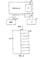
- Figure 1 shows a block diagram of a digital system within which the present invention may be embodied.
- the system may be provided on a single board, on multiple boards, or even within multiple enclosures.
- Figure 1 illustrates a system 101 in which a programmable logic device 121 may be utilized.
- Programmable logic devices are sometimes referred to as a PALs, PLAs, FPLAs, PLDs, CPLDs, EPLDs, EEPLDs, LCAs, or FPGAs and are well-known integrated circuits that provide the advantages of fixed integrated circuits with the flexibility of custom integrated circuits.
- Such devices allow a user to electrically program standard, off-the-shelf logic elements to meet a user's specific needs. See, for example, U.S.
- a processing unit 101 is coupled to a memory 105 and an I/O 111 and incorporates a programmable logic device (PLD) 121.
- PLD 121 may be specially coupled to memory 105 through connection 131 and to I/O111 through connection 135.
- the system may be a programmed digital computer system, digital signal processing system, specialized digital switching network, or other processing system.
- such systems may be designed for a wide variety of applications such as, merely by way of example, telecommunications systems, automotive systems, control systems, consumer electronics, personal computers, and others.
- Processing unit 101 may direct data to an appropriate system component for processing or storage, execute a program stored in memory 105 or input using I/O 111, or other similar function.
- Processing unit 101 may be a central processing unit (CPU), microprocessor, floating point coprocessor, graphics coprocessor, hardware controller, microcontroller, programmable logic device programmed for use as a controller, or other processing unit.
- CPU central processing unit
- PLDs 121 may control the logical operations of the system.
- processing unit 101 may even be a computer system.
- Memory 105 may be a random access memory (RAM), read only memory (ROM), fixed or flexible disk media, PC Card flash disk memory, tape, or any other storage retrieval means, or any combination of these storage retrieval means.
- PLD 121 may serve many different purposes within the system in Figure 1 .
- PLD 121 may be a logical building block of processing unit 101, supporting its internal and external operations. PLD 121 is programmed to implement the logical functions necessary to carry on its particular role in system operation.
- FIG 2 is a simplified block diagram of an overall internal architecture and organization of PLD 121 of Figure 1 . Many details of PLD architecture, organization, and circuit design are not necessary for an understanding of the present invention and such details are not shown in Figure 2 .
- Figure 2 shows a six-by-six two-dimensional array of thirty-six logic array blocks (LABs) 200.
- LAB 200 is a physically grouped set of logical resources that is configured or programmed to perform logical functions.
- the internal architecture of a LAB will be described in more detail below in connection with Figure 3 .
- PLDs may contain any arbitrary number of LABs, more or less than shown in PLD 121 of Figure 2 .
- LABs 200 need not be organized in a square matrix or array, for example, the array may be organized in a five-by-seven or a twenty-by-seventy matrix of LABs.
- LAB 200 has inputs and outputs (not shown) which may or may not be programmably connected to a global interconnect structure, comprising an array of global horizontal interconnects (GHs) 210 and global vertical interconnects (GVs) 220. Although shown as single lines in Figure 2 , each GH 210 and GV 220 line may represent a plurality of signal conductors. The inputs and outputs of LAB 200 are programmably connectable to an adjacent GH 210 and an adjacent GV 220. Utilizing GH 210 and GV 220 interconnects, multiple LABs 200 may be connected and combined to implement larger, more complex logic functions than can be realized using a single LAB 200.
- GHs global horizontal interconnects
- GVs global vertical interconnects
- GH 210 and GV 220 conductors may or may not be programmably connectable at intersections 225 of these conductors. Moreover, GH 210 and GV 220 conductors may make multiple connections to other GH 210 and GV 220 conductors. Various GH 210 and GV 220 conductors may be programmably connected together to create a signal path from a LAB 200 at one location on PLD 121 to another LAB 200 at another location on PLD 121. A signal may pass through a plurality of intersections 225. Furthermore, an output signal from one LAB 200 can be directed into the inputs of one or more LABs 200.
- signals from a LAB 200 can be fed back into the same LAB 200.
- only selected GH 210 conductors are programmably connectable to a selection of GV 220 conductors.
- GH 210 and GV 220 conductors may be specifically used for passing signal in a specific direction, such as input or output, but not both.
- the programmable logic integrated circuit may include special or segmented interconnect that is connected to a specific number of LABs and not necessarily an entire row or column of LABs.
- the segmented interconnect may programmably connect two, three, four, five, or more LABs.
- the PLD architecture in Figure 2 further shows at the peripheries of the chip, input-output drivers 230.
- Input-output drivers 230 are for interfacing the PLD to external, off-chip circuitry.
- Figure 2 shows thirty-two input-output drivers 230; however, a PLD may contain any number of input-output drivers, more or less than the number depicted.
- Each input-output driver 230 is configurable for use as an input driver, output driver, or bidirectional driver.
- the input-output drivers may be embedded with the integrated circuit core itsclf. This embedded placement of the input-output drivers may be used with flip chip packaging and will minimize the parasitics of routing the signals to input-output drivers.
- Figure 3 shows a simplified block diagram of LAB 200 of Figure 2 .
- LAB 200 is comprised of a varying number of logic elements (LEs) 300, sometimes referred to as "logic cells," and a local (or internal) interconnect structure 310.
- LEs logic elements
- LAB 200 has eight LEs 300, but LAB 200 may have any number of LEs, more or less than eight.
- LE 300 is the smallest logical building block of a PLD. Signals external to the LAB, such as from GHs 210 and GVs 220, are programmably connected to LE 300 through local interconnect structure 310.
- LE 300 of the present invention incorporates a function generator that is configurable to provide a logical function of a number of variables, such a four-variable Boolean operation. As well as combinatorial functions, LE 300 also provides support for sequential and registered functions using, for example, D flip-flops.
- LE 300 provides combinatorial and registered outputs that are connectable to the GHs 210 and GVs 220, outside LAB 200. Furthermore, the outputs from LE 300 may be internally fed back into local interconnect structure 310; through local interconnect structure 310, an output from one LE 300 may be programmably connected to the inputs of other LEs 300, without using the global interconnect structure's GHs 210 and GVs 220. Local interconnect structure 310 allows short-distance interconnection of LEs, without utilizing the limited global resources, GHs 210 and GVs 220.
- FIG. 4 shows a PLD architecture similar to that in Figure 2 .
- the architecture in Figure 4 further includes embedded array blocks (EABs).
- EABs contain user memory, a flexible block of RAM. More discussion of this architecture may be found in the Altera Data Book (1999) in the description of the FLEX 10K product family and also in U.S. patent number 5,550,782 , which are incorporated by reference.
- Figure 5 shows a further embodiment of a programmable logic integrated circuit architecture.
- Figure 5 only shows a portion of the architecture. The features shown in Figure 5 are repeated horizontally and vertically as needed to create a PLD of any desired size.
- a number of LABs are grouped together into a megaLAB.
- a megaLAB has sixteen LABs, each of which has ten LEs.
- a megaLAB is programmably connected using a megaLAB interconnect. This megaLAB interconnect may be considered another interconnect level that is between the global interconnect and local interconnect levels.
- the megaLAB interconnect can be programmably connected to GVs, GHs, and the local interconnect of each LAB of the megaLAB.
- a megaLAB Compared to the architecture of Figure 2 , this architecture has an additional level of interconnect, the megaLAB interconnect.
- Such an architecture is found in Altera's APEXTM family of products, which is described in detail in the APEX20K Programmable Logic Device Family Data Sheet (August 1999), which is incorporated by reference.
- a megaLAB also includes an embedded system block (ESB) to implement a variety of memory functions such as CAM, RAM, dual-port RAM, ROM, and FIFO functions.
- ESD embedded system block
- VCC voltages for integrated circuits continue to change and generally are being reduced.
- Some VCC voltages today are 5 volts, 3.3 volts, 2.5 volts, and 1.8 volts.
- VOH and other I/O parameters For each of these VCC, there is also an accompanying specification for VOH and other I/O parameters.
- one group of I/O pins may be used to support a particular VCC and VOH standard while another group supports another standard.
- some I/O pins may be used for the 5-volt standards while other I/O pins are for use with the 3.3-volt standard.
- It is important that the output buffer circuitry is adaptable to facilitate compatibility with multiple and changing standards.
- One technique to implement multiple standards is to use different VCCs for different I/O pins. However, this technique requires separate I/O buffers for each standard, which will take more integrated circuit area.
- FIGS 6 and 7 show two implementations of output buffer circuitry to provide a configurable VOH voltage. By providing a configurable VOH voltage, this reduces the amount of integrated circuit area used because separate buffers for each of the different VCCs is no longer needed.
- the circuits shown in Figures 6 and 7 may be used to implement the configurable I/O cell of a programmable logic device
- the I/O buffers in Figures 6 and 7 are simplified to better illustrate of the principles of the present invention. The techniques of these two circuits can also be combmed into a single circuit to benefit from each implementation's strengths.
- a VREF voltage is shown in the Figures 6 and 7 .
- This VREF voltage may be generated internally within the integrated circuit.
- VREF may be supplied from the supply voltage of the destination integrated circuit the I/O buffer will be driving.
- different I/O pins of the same integrated circuit may support multiple LVTTL I/O standards.
- the particular I/O pin will be connected to the appropriate VREF voltage.
- the VREF voltage may be generated using a programmable VREF generator. By programming the VREF generator appropriately, an I/O can be set to conform to a desired LVTTL I/O standard.
- the VREF generated can be made programmable with enough gradations in settings so new LVTTL standards can be supported.
- the VREF generator is programmed to generate a VREF voltage level to set the VOH to meet the new standard. This is particularly easy to implement in programmable logic integrated circuits (e.g., FPGAs, PLDs, memories, EPROMs, EEPROMs, Flash EEPROMs) since these devices are programmed before use. Therefore, programming of these devices is already part of their use.
- the output drivers are a PMOS transistor 605 and NMOS transistor 607. These transistors are driven by a predriver circuit 610.
- Transistor 605 is connected to VCCN through a NMOS transistor TN1.
- VCCN is a noisy VCC.
- VCCN is used in a integrated circuit implementation where there is a VCCQ or quiet VCC for internal circuitry and VCCN for the I/O circuitry. By providing separate VCCQ and VCCN pins, this helps isolate noisy circuitry from the circuitry that may be sensitive to power supply noise. Other integrated circuit implementation may only have a VCC pin for both noisy and quiet circuitry.
- Predriver circuit drives transistors 605 and 607 to cause output node 620 to be high, low, or tristate.
- a gate of transistor TN1 is supplied with a voltage VREF + VTN1, where VTN1 is the threshold voltage of the TN1 device. Consequently, if VREF is less than VCCN, the source of transistor- 605 will be at about VREF. If VCCN is less than VREF, then the source of transistor 605 will be about VCCN. Therefore, the VOH voltage at an output node 620 will be the lesser of either VREF or VCCN.
- transistor TN1 In order to obtain good transient characteristics, transistor TN1 should be quite large. In one implementation, transistor TN1 is about ten times larger in size than PMOS transistor 605. One reason why a relatively large TN1 is needed is because the TN1 device is likely to be barely on. A larger-sized device will supply greater current, especially when the device is not fully on.
- the implementation in Figure 7 is a technique to obtain a configurable VOH circuit without using the TN1 transistor of the Figure 6 circuit.
- An output 720 is taken from between transistors 705 and 707.
- An A input of a differential amplifier 205 is connected to an output node 720.
- a B input of differential amplifier 205 is connected to a VREF voltage.
- An output C of the differential amplifier is connected to a logic gate 230.
- logic gate 230 is an OR gate.
- other types of logic gates may be used to implement a similar function. For example, pass transistors may be used instead.
- the differential amplifier will output a logic level of 12 if a voltage at A is greater than a voltage at B and a 0 otherwise. Therefore, the VOH voltage at output node 220 will be the lesser of either Vref or VCCN.
- Figure 7 may optionally include a leaker device 735 to maintain VOH statically.
- the leaker device would be a relatively small-sized transistor to ensure the output high voltage is above the VIH required for input by another integrated circuit.
- Another technique is to dynamically maintain VOH by using PMOS transistor 705.
- a standard I/O cell can be placed in parallel with the Figure 7 circuitry at output node 720.
- the standard I/O cell would provide standard VCCN support while the circuitry in Figure 7 would provide support for multiple I/O standards.
- Figure 8 is a block diagram of such an implementation.
- I/O circuit 230 includes both a standard I/O cell and multiple standard I/O circuit.
- the multiple standard circuit may include the circuitry shown in Figure 6 or 7 , or both, as well as other circuit technique to implement an multiple I/O standard output circuit.
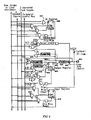
- Figure 9 shows a specific implementation of a standard I/O cell. This implementation is especially designed for use in a programmable logic device because of the flexible logic, but may also be used in other types of integrated circuits.
- the I/O cell of FIG. 9 is interfaced to dedicated inputs, dedicated clock inputs, a peripheral control bus, and a row, column, or local interconnect, as shown by the signal lines at the upper left corner of the figure.
- the I/O cell has an input register 910 and output buffer 920 coupled to pad 902.
- a first multiplexing circuit 922 has an output that is coupled to the input of the output buffer 920 through a programmable delay line 924.
- the first multiplexing circuit 922 has a first input coupled to a signal line 923 and a second input coupled to an output of an output register 930.
- the register 930 may be clocked by clock signals on the dedicated clock inputs or the peripheral control bus by way of a multiplexing circuit 932.
- the input of register 930 is provided by an output of a second multiplexing circuit 934, which receives the signal on signal line 923 and the output of output buffer 920 through respective programmable delay lines.
- the signal on signal line 923 is provided by the output of a third multiplexing circuit 926, which is configured to selectively couple to a logic element (via the row, column, local interconnect and the dedicated inputs), and thereby couple the logic element to respective inputs of the first and second multiplexing circuits 922 and 934.
- Output buffer 920 has a tristate control input that is coupled to the output of an output-enable (OE) register 950.
- the input of the OE register 950 is coupled to an output of a third multiplexing circuit 952 that is configured to selectively couple one of a plurality of logic elements (via the row, column, local interconnect and the dedicated inputs) to the input of register 950.
- the first multiplexing circuit 922 may be configured to selectively couple either an output of the first register 930 or an input of the first register 930 to an input of the output buffer 920.
- the first register 930 may be clocked by a clock signal selected by multiplexer circuit 932.
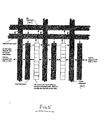
- FIG 10 shows a number of I/O circuits of an integrated circuit. All of the I/O circuits are connected to the same supply voltage, VCCN. The supply voltage should be the highest supply voltage needed by any of the I/O standards. Two of the I/O circuits 1015 are connected to a first VREF voltage VREF1 and two of the I/O circuits 1025 are connected to a second VREF voltage VREF2.
- I/O circuitry of the present invention such as shown in Figure 6 or 7 , I/O circuits 1015 will be compatible with a first I/O standard and I/O circuits 1025 will be compatible with a second I/O standard.
- the first and second I/O standards are different while a single supply voltage VCCN is supplied to all the I/O circuits.
- the circuitry of the present invention eliminates the need to use different supply voltages to be compatible with different I/O standards. Among the many advantages of this circuitry, this circuitry saves space on the integrated circuit.
Landscapes
- Engineering & Computer Science (AREA)
- Physics & Mathematics (AREA)
- Mathematical Physics (AREA)
- Computer Hardware Design (AREA)
- Computing Systems (AREA)
- General Engineering & Computer Science (AREA)
- Computer Networks & Wireless Communication (AREA)
- Logic Circuits (AREA)
- Semiconductor Integrated Circuits (AREA)
- Design And Manufacture Of Integrated Circuits (AREA)
Abstract
Description
- This application claims the benefit of
U.S. provisional application 60/126,235 filed March 24, 1999 - The present invention relates to the field of integrated circuits and more specifically, to output buffer circuitry capable of operating at the output voltage levels needed for a particular application.
- As semiconductor processing technology continues to advance, integrated circuits or "chips" continue to provide greater functionality and performance. Examples of some integrated circuits include microprocessors, application specific integrated circuits (ASICs), programmable logic devices (PLDs), field programmable gate arrays (FPGAs), and memories such as dynamic random access memories (DRAMs), static random access memories (SRAMs), and nonvolatile memories (Flash and EEPROM). The positive power supply voltage used for integrated circuits of different process technologies is often different. Generally, newer process technologies use reduced positive power supply voltages. For example, previous generation integrated circuit used a supply voltage, VDD or VCC, or 5 volts. More recent integrated circuits used 3.3- and 3-volt power supplies. Some current integrated circuits use 2.5-volt power supplies. In the future, it is expected supply voltages will be further reduced to 2 volts and lower. Therefore, each generation of integrated circuits is compatible with a particular power supply voltage and input and output standard.
- In an electronic system, it is often desirable that an integrated circuit compatible with one input-output standard can be used with integrated circuits of other input-output standards. Among the many advantages of having such a chip, the integrated circuit customer can used that particular chip on a system board with chips of other input-output standards. The integrated circuit manufacturer can produce one chip that is compatible with current and previous generation technology.
- Furthermore, when there are emerging I/O standards for integrated circuits such as for a low voltage TTL (LVTTL) output or low voltage differential signal (LVDS) output, the different standards often have different voltages for VOH and VOL. Until a uniform standard is adapted, it is desirable for integrated circuit makers to design their products to be compatible with as many of the standards as possible. This will increase the overall potential market for a particular product.
- Therefore, there is a need for an output circuitry that is adaptable or configurable to different I/O standards.
- The present invention provides circuitry to individually configure each I/O of an integrated circuit to different LVTTL I/O standards. This is done with only one I/O supply voltage, where that voltage is the highest of the I/O voltages needed in a particular application. The invention operates by regulating the output voltage of the I/O cell so that it is above the VOH and below the maximum VIH for the LVTTL standard for which it will comply with. Since each I/O cell is individually configurable, any I/O can drive out to any LVTTL specification.
- In an embodiment, the present invention is a programmable logic integrated circuit including a group of first I/O circuits connected to a supply voltage and a first configurable reference voltage. There is also a group of second I/O circuits connected to the supply voltage and a second configurable reference voltage. The first configurable reference voltage is different from the second configurable reference voltage. The group of first I/O circuits is compatible with a first I/O voltage standard based on the first configurable reference voltage and the group of second I/O circuits compatible with a second I/O voltage standard based on the second configurable reference voltage.
- In one implementation, each I/O circuit includes a first transistor connected between the supply voltage and a first node with a control electrode connected to a voltage level equal to the first reference voltage plus a threshold voltage of the first transistor. The circuitry includes a second transistor connected between the first node and a pad and a third transistor connected between the pad and ground. In a specific circuit implementation, the first transistor is NMOS, the second transistor in PMOS, and the first transistor is at least about ten times larger in size than the second transistor. In other implementation, the first transistor may be less than ten times larger than the second transistor.
- In another implementation, each I/O circuit includes a first transistor connected between the supply voltage and a pad. A second transistor is connected between the pad and ground. A logic gate has an output connected to a control electrode of the first transistor. And, a differential amplifier circuit has a first input connected to the pad and a second input connected to the second reference voltage. The differential amplifier provides an output to an input of the logic gate, where the output is a logic high when a voltage at the second input is higher than a voltage at the first input and the output is a logic low when the voltage at the first input is higher than the voltage at the second input.
- In another embodiment, the invention is a method of operating a programmable logic integrated circuit. A first reference voltage level is programmably selected to be connected to a first I/O circuit to select a first I/O standard the first I/O circuit will be compatible with. A second reference voltage level is programmably selected to be connected to a second I/O circuit to select a second I/O standard the second I/O circuit will be compatible with.
- In another embodiment, the invention is an integrated circuit including a first transistor connected between a supply voltage and a first node, where a control electrode of the first transistor is connected to a reference voltage. A second transistor is connected between the first node and an output pad of the integrated circuit, where a voltage output high level at the pad will be the lesser of the reference voltage level or the supply voltage.
- In another embodiment, the invention is an integrated circuit including a differential amplifier having a first input connected to a pad of the integrated circuit and a second input connected to a reference voltage. A pull-up transistor is connected between a supply voltage and the pad. And a logic gate having an output connected to a control electrode of the pull-up transistor and an input is connected to an output of the differential amplifier.
- Other objects, features, and advantages of the present invention will become apparent upon consideration of the following detailed description and the accompanying drawings, in which like reference designations represent like features throughout the figures.
- Embodiments of the invention include:
-
Statement 1. A programmable logic integrated circuit comprising:- a plurality of first I/O circuits coupled to a supply voltage and a first configurable reference voltage; and
- a plurality of second I/O circuits coupled to the supply voltage and a second configurable reference voltage, wherein the first configurable reference voltage is different from the second configurable reference voltage and the plurality of first I/O circuits is compatible with a first I/O standard based on the first configurable reference voltage and the plurality of second I/O circuits compatible with a second I/O voltage standard based on the second configurable reference voltage.
-
Statement 2. An integrated circuit as defined instatement 1 wherein each of the plurality of first I/O circuits comprises:- a first transistor coupled between the supply voltage and a first node, and having a control electrode coupled to a voltage level equal to the first reference voltage plus a threshold voltage of the first transistor;
- a second transistor coupled between the first node and a pad; and
- a third transistor coupled between the pad and ground.
- Statement 3. An integrated circuit as defined in
statement 2 wherein the first transistor is NMOS and the second transistor in PMOS, and the first transistor is at least about ten times larger in size than the second transistor. -
Statement 4. An integrated circuit as defined instatement 2 wherein a VOH of the first I/O circuit is the lesser of the first reference voltage or the supply voltage. - Statement 5. An integrated circuit as defined in
statement 1 wherein each of the plurality of second I/O circuits comprises:- a first transistor coupled between the supply voltage and a pad;
- a second transistor coupled between the pad and ground;
- a logic gate having an output coupled to a control electrode of the first transistor; and
- a differential amplifier circuit having a first input coupled to the pad and a second input coupled to the second reference voltage, and providing an output to an input of the logic gate, wherein the output is a logic high when a voltage at the second input is higher than a voltage at the first input, and the output is a logic low when the voltage at the first input is higher than the voltage at the second input.
- Statement 6. An integrated circuit as defined in statement 5 wherein a VOH of the second I/O circuit is the lesser of the second reference voltage or the supply voltage.
- Statement 7. An integrated circuit as defined in statement 5 wherein the second I/O circuit further comprises a leaker device coupled between the supply voltage and the pad to statically hold a VOH voltage at the pad.
- Statement 8. An integrated circuit as defined in statement 5 wherein the logic gate further comprises an input coupled to a predriver circuit.
- Statement 9. An integrated circuit as defined in statement 7 wherein the first transistor and leaker device are PMOS transistors and the first transistor is larger in size than the leaker device.
-
Statement 10. An integrated circuit as defined instatement 1 wherein the first configurable reference voltage is programmably selectable by configuring memory cells of the integrated circuit. - Statement 11. An integrated circuit as defined in
statement 1 wherein the first and second I/O circuits each comprise:- a first multiplexer having a first input programmably coupled to an interconnect line and a second input coupled to a pad;
- an output register having a input coupled to an output of the first multiplexer; and
- a second multiplexer having a first input programmably coupled to the interconnect line and a second input coupled to an output of the output register, and providing an output to the pad.
-
-
Figure 1 is a diagram of a digital system with a programmable logic integrated circuit: -
Figure 2 is a diagram showing an architecture of a programmable logic integrated circuit; -
Figure 3 is a simplified block diagram of a logic array block (LAB); -
Figure 4 shows an architecture of a programmable logic integrated circuit with embedded array blocks (EABs); -
Figure 5 shows an architecture of a programmable logic integrated circuit with megaLABs; -
Figure 6 shows a first circuit implementation of output buffer circuitry configurable to multiple I/O standards; -
Figure 7 shows a second circuit implementation of output buffer circuitry configurable to multiple I/O standards; -
Figure 8 shows a I/O configuration circuit including a standard I/O buffer circuit and a multiple standard I/O buffer circuit; -
Figure 9 shows an implementation of an I/O buffer circuit; and -
Figure 10 shows I/O circuits of an integrated circuit connected to the same supply voltage and compatible with more than one different I/O standard. -
Figure 1 shows a block diagram of a digital system within which the present invention may be embodied. The system may be provided on a single board, on multiple boards, or even within multiple enclosures.Figure 1 illustrates asystem 101 in which aprogrammable logic device 121 may be utilized. Programmable logic devices are sometimes referred to as a PALs, PLAs, FPLAs, PLDs, CPLDs, EPLDs, EEPLDs, LCAs, or FPGAs and are well-known integrated circuits that provide the advantages of fixed integrated circuits with the flexibility of custom integrated circuits. Such devices allow a user to electrically program standard, off-the-shelf logic elements to meet a user's specific needs. See, for example,U.S. patent number 4,617,479 , incorporated by reference for all purposes. Programmable logic devices are currently represented by, for example, Alter's MAX®, FLEX®, and APEX™ series of PLDs. These are described in, for example,U.S. patent numbers 4,871,930 ,5,241,224 ,5,258,668 ,5,260,610 ,5,260,611 ,5,436,575 , and the Altera Data Book (1999), all incorporated by reference in their entirety for all purposes. Programmable logic integrated circuits and their operation are well known to those of skill in the art. - In the particular embodiment of
Figure 1 , aprocessing unit 101 is coupled to amemory 105 and an I/O 111 and incorporates a programmable logic device (PLD) 121.PLD 121 may be specially coupled tomemory 105 throughconnection 131 and to I/O111 throughconnection 135. The system may be a programmed digital computer system, digital signal processing system, specialized digital switching network, or other processing system. Moreover, such systems may be designed for a wide variety of applications such as, merely by way of example, telecommunications systems, automotive systems, control systems, consumer electronics, personal computers, and others. -
Processing unit 101 may direct data to an appropriate system component for processing or storage, execute a program stored inmemory 105 or input using I/O 111, or other similar function.Processing unit 101 may be a central processing unit (CPU), microprocessor, floating point coprocessor, graphics coprocessor, hardware controller, microcontroller, programmable logic device programmed for use as a controller, or other processing unit. Furthermore, in many embodiments, there is often no need for a CPU. For example, instead of a CPU, one ormore PLDs 121 may control the logical operations of the system. In some embodiments, processingunit 101 may even be a computer system.Memory 105 may be a random access memory (RAM), read only memory (ROM), fixed or flexible disk media, PC Card flash disk memory, tape, or any other storage retrieval means, or any combination of these storage retrieval means.PLD 121 may serve many different purposes within the system inFigure 1 .PLD 121 may be a logical building block ofprocessing unit 101, supporting its internal and external operations.PLD 121 is programmed to implement the logical functions necessary to carry on its particular role in system operation. -
Figure 2 is a simplified block diagram of an overall internal architecture and organization ofPLD 121 ofFigure 1 . Many details of PLD architecture, organization, and circuit design are not necessary for an understanding of the present invention and such details are not shown inFigure 2 . -
Figure 2 shows a six-by-six two-dimensional array of thirty-six logic array blocks (LABs) 200.LAB 200 is a physically grouped set of logical resources that is configured or programmed to perform logical functions. The internal architecture of a LAB will be described in more detail below in connection withFigure 3 . PLDs may contain any arbitrary number of LABs, more or less than shown inPLD 121 ofFigure 2 . Generally in the future, as technology advances and improves, programmable logic devices with greater numbers of logic array blocks will undoubtedly be created. Furthermore,LABs 200 need not be organized in a square matrix or array, for example, the array may be organized in a five-by-seven or a twenty-by-seventy matrix of LABs. -
LAB 200 has inputs and outputs (not shown) which may or may not be programmably connected to a global interconnect structure, comprising an array of global horizontal interconnects (GHs) 210 and global vertical interconnects (GVs) 220. Although shown as single lines inFigure 2 , eachGH 210 andGV 220 line may represent a plurality of signal conductors. The inputs and outputs ofLAB 200 are programmably connectable to anadjacent GH 210 and anadjacent GV 220. UtilizingGH 210 andGV 220 interconnects,multiple LABs 200 may be connected and combined to implement larger, more complex logic functions than can be realized using asingle LAB 200. - In one embodiment,
GH 210 andGV 220 conductors may or may not be programmably connectable atintersections 225 of these conductors. Moreover,GH 210 andGV 220 conductors may make multiple connections toother GH 210 andGV 220 conductors.Various GH 210 andGV 220 conductors may be programmably connected together to create a signal path from aLAB 200 at one location onPLD 121 to anotherLAB 200 at another location onPLD 121. A signal may pass through a plurality ofintersections 225. Furthermore, an output signal from oneLAB 200 can be directed into the inputs of one ormore LABs 200. Also, using the global interconnect, signals from aLAB 200 can be fed back into thesame LAB 200. In specific embodiments of the present invention, only selectedGH 210 conductors are programmably connectable to a selection ofGV 220 conductors. Furthermore, in still further embodiments,GH 210 andGV 220 conductors may be specifically used for passing signal in a specific direction, such as input or output, but not both. - In other embodiments, the programmable logic integrated circuit may include special or segmented interconnect that is connected to a specific number of LABs and not necessarily an entire row or column of LABs. For example, the segmented interconnect may programmably connect two, three, four, five, or more LABs.
- The PLD architecture in
Figure 2 further shows at the peripheries of the chip, input-output drivers 230. Input-output drivers 230 are for interfacing the PLD to external, off-chip circuitry.Figure 2 shows thirty-two input-output drivers 230; however, a PLD may contain any number of input-output drivers, more or less than the number depicted. Each input-output driver 230 is configurable for use as an input driver, output driver, or bidirectional driver. In other embodiments of a programmable logic integrated circuit, the input-output drivers may be embedded with the integrated circuit core itsclf. This embedded placement of the input-output drivers may be used with flip chip packaging and will minimize the parasitics of routing the signals to input-output drivers. -
Figure 3 shows a simplified block diagram ofLAB 200 ofFigure 2 .LAB 200 is comprised of a varying number of logic elements (LEs) 300, sometimes referred to as "logic cells," and a local (or internal)interconnect structure 310.LAB 200 has eightLEs 300, butLAB 200 may have any number of LEs, more or less than eight. - A general overview of
LE 300 is presented here, sufficient to provide a basic understanding of the present invention.LE 300 is the smallest logical building block of a PLD. Signals external to the LAB, such as fromGHs 210 andGVs 220, are programmably connected toLE 300 throughlocal interconnect structure 310. In one embodiment,LE 300 of the present invention incorporates a function generator that is configurable to provide a logical function of a number of variables, such a four-variable Boolean operation. As well as combinatorial functions,LE 300 also provides support for sequential and registered functions using, for example, D flip-flops. -
LE 300 provides combinatorial and registered outputs that are connectable to theGHs 210 andGVs 220, outsideLAB 200. Furthermore, the outputs fromLE 300 may be internally fed back intolocal interconnect structure 310; throughlocal interconnect structure 310, an output from oneLE 300 may be programmably connected to the inputs ofother LEs 300, without using the global interconnect structure'sGHs 210 andGVs 220.Local interconnect structure 310 allows short-distance interconnection of LEs, without utilizing the limited global resources,GHs 210 andGVs 220. -
Figure 4 shows a PLD architecture similar to that inFigure 2 . The architecture inFigure 4 further includes embedded array blocks (EABs). EABs contain user memory, a flexible block of RAM. More discussion of this architecture may be found in the Altera Data Book (1999) in the description of the FLEX 10K product family and also inU.S. patent number 5,550,782 , which are incorporated by reference. -
Figure 5 shows a further embodiment of a programmable logic integrated circuit architecture.Figure 5 only shows a portion of the architecture. The features shown inFigure 5 are repeated horizontally and vertically as needed to create a PLD of any desired size. In this architecture, a number of LABs are grouped together into a megaLAB. In a specific embodiment, a megaLAB has sixteen LABs, each of which has ten LEs. There can be any number of megaLABs per PLD. A megaLAB is programmably connected using a megaLAB interconnect. This megaLAB interconnect may be considered another interconnect level that is between the global interconnect and local interconnect levels. The megaLAB interconnect can be programmably connected to GVs, GHs, and the local interconnect of each LAB of the megaLAB. Compared to the architecture ofFigure 2 , this architecture has an additional level of interconnect, the megaLAB interconnect. Such an architecture is found in Altera's APEX™ family of products, which is described in detail in the APEX20K Programmable Logic Device Family Data Sheet (August 1999), which is incorporated by reference. In a specific implementation, a megaLAB also includes an embedded system block (ESB) to implement a variety of memory functions such as CAM, RAM, dual-port RAM, ROM, and FIFO functions. - VCC voltages for integrated circuits continue to change and generally are being reduced. Some VCC voltages today are 5 volts, 3.3 volts, 2.5 volts, and 1.8 volts. For each of these VCC, there is also an accompanying specification for VOH and other I/O parameters. For some integrated circuits, one group of I/O pins may be used to support a particular VCC and VOH standard while another group supports another standard. For example, some I/O pins may be used for the 5-volt standards while other I/O pins are for use with the 3.3-volt standard. It is important that the output buffer circuitry is adaptable to facilitate compatibility with multiple and changing standards. One technique to implement multiple standards is to use different VCCs for different I/O pins. However, this technique requires separate I/O buffers for each standard, which will take more integrated circuit area.
- Another technique is to use a single VCC voltage and to configure the circuitry to provide a desired voltage output high (VOH) voltage to support a particular standard.
Figures 6 and 7 show two implementations of output buffer circuitry to provide a configurable VOH voltage. By providing a configurable VOH voltage, this reduces the amount of integrated circuit area used because separate buffers for each of the different VCCs is no longer needed. The circuits shown inFigures 6 and 7 may be used to implement the configurable I/O cell of a programmable logic device The I/O buffers inFigures 6 and 7 are simplified to better illustrate of the principles of the present invention. The techniques of these two circuits can also be combmed into a single circuit to benefit from each implementation's strengths. - A VREF voltage is shown in the
Figures 6 and 7 . This VREF voltage may be generated internally within the integrated circuit. Or, VREF may be supplied from the supply voltage of the destination integrated circuit the I/O buffer will be driving. There will be a VREF voltage for each LVTTL I/O standard supported. For example, different I/O pins of the same integrated circuit may support multiple LVTTL I/O standards. The particular I/O pin will be connected to the appropriate VREF voltage. Also, the VREF voltage may be generated using a programmable VREF generator. By programming the VREF generator appropriately, an I/O can be set to conform to a desired LVTTL I/O standard. - There is also the likelihood the LVTTL specifications for emerging supply voltage standards will be defined in the future with lower VOH and VIH max values than used presently. The technique of the present invention will allow the integrated circuit to adapt to these yet undefined and unavailable standards. If the VREF comes from the destination integrated circuit, new LVTTL standards can be immediately supported with existing integrated circuit's containing this invention by applying the new supply voltage of the destination device to the invention integrated circuit's VREF.
- If the VREF is generated on-chip, the VREF generated can be made programmable with enough gradations in settings so new LVTTL standards can be supported. The VREF generator is programmed to generate a VREF voltage level to set the VOH to meet the new standard. This is particularly easy to implement in programmable logic integrated circuits (e.g., FPGAs, PLDs, memories, EPROMs, EEPROMs, Flash EEPROMs) since these devices are programmed before use. Therefore, programming of these devices is already part of their use.
- In the
Figure 6 embodiment, the output drivers are aPMOS transistor 605 andNMOS transistor 607. These transistors are driven by apredriver circuit 610.Transistor 605 is connected to VCCN through a NMOS transistor TN1. VCCN is a noisy VCC. VCCN is used in a integrated circuit implementation where there is a VCCQ or quiet VCC for internal circuitry and VCCN for the I/O circuitry. By providing separate VCCQ and VCCN pins, this helps isolate noisy circuitry from the circuitry that may be sensitive to power supply noise. Other integrated circuit implementation may only have a VCC pin for both noisy and quiet circuitry. - Predriver circuit drives
transistors output node 620 to be high, low, or tristate. A gate of transistor TN1 is supplied with a voltage VREF + VTN1, where VTN1 is the threshold voltage of the TN1 device. Consequently, if VREF is less than VCCN, the source of transistor- 605 will be at about VREF. If VCCN is less than VREF, then the source oftransistor 605 will be about VCCN. Therefore, the VOH voltage at anoutput node 620 will be the lesser of either VREF or VCCN. - In order to obtain good transient characteristics, transistor TN1 should be quite large. In one implementation, transistor TN1 is about ten times larger in size than
PMOS transistor 605. One reason why a relatively large TN1 is needed is because the TN1 device is likely to be barely on. A larger-sized device will supply greater current, especially when the device is not fully on. - The implementation in
Figure 7 is a technique to obtain a configurable VOH circuit without using the TN1 transistor of theFigure 6 circuit. InFigure 7 , there are outputdrivers PMOS transistor 705 andNMOS transistor 707, which are connected in series between VCCN and ground. Anoutput 720 is taken from betweentransistors output node 720. And, a B input of differential amplifier 205 is connected to a VREF voltage. An output C of the differential amplifier is connected to alogic gate 230. In this implementation,logic gate 230 is an OR gate. However, other types of logic gates may be used to implement a similar function. For example, pass transistors may be used instead. The differential amplifier will output a logic level of 12 if a voltage at A is greater than a voltage at B and a 0 otherwise. Therefore, the VOH voltage atoutput node 220 will be the lesser of either Vref or VCCN. -
Figure 7 may optionally include aleaker device 735 to maintain VOH statically. The leaker device would be a relatively small-sized transistor to ensure the output high voltage is above the VIH required for input by another integrated circuit. Another technique is to dynamically maintain VOH by usingPMOS transistor 705. For the highest performance when usingFigure 7 , a standard I/O cell can be placed in parallel with theFigure 7 circuitry atoutput node 720. The standard I/O cell would provide standard VCCN support while the circuitry inFigure 7 would provide support for multiple I/O standards.Figure 8 is a block diagram of such an implementation. I/O circuit 230 includes both a standard I/O cell and multiple standard I/O circuit. The multiple standard circuit may include the circuitry shown inFigure 6 or 7 , or both, as well as other circuit technique to implement an multiple I/O standard output circuit. -
Figure 9 shows a specific implementation of a standard I/O cell. This implementation is especially designed for use in a programmable logic device because of the flexible logic, but may also be used in other types of integrated circuits.
The I/O cell ofFIG. 9 is interfaced to dedicated inputs, dedicated clock inputs, a peripheral control bus, and a row, column, or local interconnect, as shown by the signal lines at the upper left corner of the figure. The I/O cell has aninput register 910 andoutput buffer 920 coupled topad 902. Afirst multiplexing circuit 922 has an output that is coupled to the input of theoutput buffer 920 through aprogrammable delay line 924. Thefirst multiplexing circuit 922 has a first input coupled to a signal line 923 and a second input coupled to an output of anoutput register 930. Theregister 930 may be clocked by clock signals on the dedicated clock inputs or the peripheral control bus by way of amultiplexing circuit 932. The input ofregister 930 is provided by an output of asecond multiplexing circuit 934, which receives the signal on signal line 923 and the output ofoutput buffer 920 through respective programmable delay lines. The signal on signal line 923 is provided by the output of a third multiplexing circuit 926, which is configured to selectively couple to a logic element (via the row, column, local interconnect and the dedicated inputs), and thereby couple the logic element to respective inputs of the first andsecond multiplexing circuits Output buffer 920 has a tristate control input that is coupled to the output of an output-enable (OE)register 950. In turn, the input of theOE register 950 is coupled to an output of athird multiplexing circuit 952 that is configured to selectively couple one of a plurality of logic elements (via the row, column, local interconnect and the dedicated inputs) to the input ofregister 950. With this configuration, thefirst multiplexing circuit 922 may be configured to selectively couple either an output of thefirst register 930 or an input of thefirst register 930 to an input of theoutput buffer 920. In the former case, thefirst register 930 may be clocked by a clock signal selected bymultiplexer circuit 932. -
Figure 10 shows a number of I/O circuits of an integrated circuit. All of the I/O circuits are connected to the same supply voltage, VCCN. The supply voltage should be the highest supply voltage needed by any of the I/O standards. Two of the I/O circuits 1015 are connected to a first VREF voltage VREF1 and two of the I/O circuits 1025 are connected to a second VREF voltage VREF2. By using the I/O circuitry of the present invention such as shown inFigure 6 or 7 , I/O circuits 1015 will be compatible with a first I/O standard and I/O circuits 1025 will be compatible with a second I/O standard. The first and second I/O standards are different while a single supply voltage VCCN is supplied to all the I/O circuits. The circuitry of the present invention eliminates the need to use different supply voltages to be compatible with different I/O standards. Among the many advantages of this circuitry, this circuitry saves space on the integrated circuit. - This description of the invention has been presented for the purposes of illustration and description. It is not intended to be exhaustive or to limit the invention to the precise form described, and many modifications and variations are possible in light of the teaching above. The embodiments were chosen and described in order to best explain the principles of the invention and its practical applications. This description will enable others skilled in the art to best utilize and practice the invention in various embodiments and with various modifications as are suited to a particular use. The scope of the invention is defined by the following claims.
Claims (15)
- An integrated circuit comprising:a plurality of first I/O circuits coupled to a supply voltage and a first reference voltage; anda plurality of second I/O circuits coupled to the supply voltage and a second reference voltage, wherein the first reference voltage is different from the second reference voltage and the plurality of first I/O circuits is compatible with a first I/O standard based on the first reference voltage and the plurality of second I/O circuits is compatible with a second I/O voltage standard based on the second reference voltage, wherein each of the I/O circuits comprise:a first register;an output buffer having an output coupled to a pad;a first multiplexing circuit configured to selectively couple either an output of the first register or an input of the first register to an input of the output buffer.
- The integrated circuit of claim 1 further comprising:a second register having an output coupled to a tristate control of the output buffer; anda second multiplexing circuit configured to selectively couple one of a plurality of logic elements to an input of the second register.
- The integrated circuit of claim 2 wherein each of the I/O circuits further comprise:a third multiplexing circuit configured to selectively couple a logic element to the input of the first register.
- The integrated circuit of claim 2 wherein each of the I/O circuits further comprise:a third multiplexing circuit configured to selectively couple one of a plurality of logic elements to a clock input of the first register.
- The integrated circuit of claim 2 wherein each of the I/O circuits further comprise:a third multiplexing circuit configured to selectively couple a logic element to the input of the first register; anda fourth multiplexing circuit configured to selectively couple one of a plurality of logic elements to a clock input of the first register.
- The integrated circuit of claim 2 wherein each of the I/O circuits further comprise:a programmable delay line coupled between the first multiplexing circuit and the output buffer.
- The integrated circuit of claim 1 further comprising:a second multiplexing circuit configured to selectively couple a logic element to the input of the first register.
- The integrated circuit of claim 7 wherein each of the I/O circuits further comprise:a second register having an output coupled to a tristate control of the output buffer.
- The integrated circuit of claim 7 wherein each of the I/O circuits further comprise:a third multiplexing circuit configured to selectively couple one of a plurality of logic elements to a clock input of the first register.
- The integrated circuit of claim 7 wherein each of the I/O circuits further comprise:a second register having an output coupled to a tristate control of the output buffer; anda third multiplexing circuit configured to selectively couple one of a plurality of logic elements to a clock input of the first register.
- The integrated circuit of claim 7 wherein each of the I/O circuits further comprise:a programmable delay line coupled between the first multiplexing circuit and the output buffer.
- The integrated circuit of claim 1 further comprising:a second multiplexing circuit configured to selectively couple one of a plurality of logic elements to a clock input of the first register.
- The integrated circuit of claim 12 wherein each of the I/O circuits further comprise:a second register having an output coupled to a tristate control of the output buffer.
- The integrated circuit of claim 13 wherein each of the I/O circuits further comprise:a third multiplexing circuit configured to selectively couple one of a plurality of logic elements to an input of the second register.
- The integrated circuit of claim 12 wherein each of the I/O circuits further comprise:a programmable delay line coupled between the first multiplexing circuit and the output buffer.
Applications Claiming Priority (2)
| Application Number | Priority Date | Filing Date | Title |
|---|---|---|---|
| US12623599P | 1999-03-24 | 1999-03-24 | |
| EP00302450A EP1039639B1 (en) | 1999-03-24 | 2000-03-24 | I/O cell configuration for multiple I/O standards |
Related Parent Applications (1)
| Application Number | Title | Priority Date | Filing Date |
|---|---|---|---|
| EP00302450.2 Division | 2000-03-24 |
Publications (1)
| Publication Number | Publication Date |
|---|---|
| EP2288030A1 true EP2288030A1 (en) | 2011-02-23 |
Family
ID=22423748
Family Applications (2)
| Application Number | Title | Priority Date | Filing Date |
|---|---|---|---|
| EP00302450A Expired - Lifetime EP1039639B1 (en) | 1999-03-24 | 2000-03-24 | I/O cell configuration for multiple I/O standards |
| EP10179941A Withdrawn EP2288030A1 (en) | 1999-03-24 | 2000-03-24 | I/O cell configuration for multiple I/O standards |
Family Applications Before (1)
| Application Number | Title | Priority Date | Filing Date |
|---|---|---|---|
| EP00302450A Expired - Lifetime EP1039639B1 (en) | 1999-03-24 | 2000-03-24 | I/O cell configuration for multiple I/O standards |
Country Status (4)
| Country | Link |
|---|---|
| US (2) | US6271679B1 (en) |
| EP (2) | EP1039639B1 (en) |
| JP (2) | JP4785224B2 (en) |
| DE (1) | DE60045230D1 (en) |
Families Citing this family (86)
| Publication number | Priority date | Publication date | Assignee | Title |
|---|---|---|---|---|
| US6825698B2 (en) * | 2001-08-29 | 2004-11-30 | Altera Corporation | Programmable high speed I/O interface |
| US6762621B1 (en) * | 1998-12-31 | 2004-07-13 | Actel Corporation | Programmable multi-standard I/O architecture for FPGAs |
| US6242943B1 (en) * | 1998-12-31 | 2001-06-05 | Khaled Ahmad El-Ayat | Programmable multi-standard I/O architecture for FPGAS |
| US6836151B1 (en) * | 1999-03-24 | 2004-12-28 | Altera Corporation | I/O cell configuration for multiple I/O standards |
| US6864710B1 (en) * | 1999-12-30 | 2005-03-08 | Cypress Semiconductor Corp. | Programmable logic device |
| US6388464B1 (en) | 1999-12-30 | 2002-05-14 | Cypress Semiconductor Corp. | Configurable memory for programmable logic circuits |
| US6608500B1 (en) * | 2000-03-31 | 2003-08-19 | Cypress Semiconductor Corp. | I/O architecture/cell design for programmable logic device |
| US6535043B2 (en) * | 2000-05-26 | 2003-03-18 | Lattice Semiconductor Corp | Clock signal selection system, method of generating a clock signal and programmable clock manager including same |
| US6487710B1 (en) * | 2000-06-30 | 2002-11-26 | Xilinx, Inc. | Method and apparatus for assigning PLD signal routes to input signals having different voltage requirements |
| US8103496B1 (en) | 2000-10-26 | 2012-01-24 | Cypress Semicondutor Corporation | Breakpoint control in an in-circuit emulation system |
| US8176296B2 (en) | 2000-10-26 | 2012-05-08 | Cypress Semiconductor Corporation | Programmable microcontroller architecture |
| US8149048B1 (en) | 2000-10-26 | 2012-04-03 | Cypress Semiconductor Corporation | Apparatus and method for programmable power management in a programmable analog circuit block |
| US7765095B1 (en) | 2000-10-26 | 2010-07-27 | Cypress Semiconductor Corporation | Conditional branching in an in-circuit emulation system |
| US6724220B1 (en) | 2000-10-26 | 2004-04-20 | Cyress Semiconductor Corporation | Programmable microcontroller architecture (mixed analog/digital) |
| US7752419B1 (en) | 2001-03-22 | 2010-07-06 | Qst Holdings, Llc | Method and system for managing hardware resources to implement system functions using an adaptive computing architecture |
| US6836839B2 (en) | 2001-03-22 | 2004-12-28 | Quicksilver Technology, Inc. | Adaptive integrated circuitry with heterogeneous and reconfigurable matrices of diverse and adaptive computational units having fixed, application specific computational elements |
| US7325123B2 (en) | 2001-03-22 | 2008-01-29 | Qst Holdings, Llc | Hierarchical interconnect for configuring separate interconnects for each group of fixed and diverse computational elements |
| US7653710B2 (en) | 2002-06-25 | 2010-01-26 | Qst Holdings, Llc. | Hardware task manager |
| US20040133745A1 (en) | 2002-10-28 | 2004-07-08 | Quicksilver Technology, Inc. | Adaptable datapath for a digital processing system |
| US7962716B2 (en) | 2001-03-22 | 2011-06-14 | Qst Holdings, Inc. | Adaptive integrated circuitry with heterogeneous and reconfigurable matrices of diverse and adaptive computational units having fixed, application specific computational elements |
| US6605962B2 (en) * | 2001-05-06 | 2003-08-12 | Altera Corporation | PLD architecture for flexible placement of IP function blocks |
| US6577678B2 (en) | 2001-05-08 | 2003-06-10 | Quicksilver Technology | Method and system for reconfigurable channel coding |
| US7406674B1 (en) | 2001-10-24 | 2008-07-29 | Cypress Semiconductor Corporation | Method and apparatus for generating microcontroller configuration information |
| US8078970B1 (en) | 2001-11-09 | 2011-12-13 | Cypress Semiconductor Corporation | Graphical user interface with user-selectable list-box |
| US8042093B1 (en) | 2001-11-15 | 2011-10-18 | Cypress Semiconductor Corporation | System providing automatic source code generation for personalization and parameterization of user modules |
| US8069405B1 (en) | 2001-11-19 | 2011-11-29 | Cypress Semiconductor Corporation | User interface for efficiently browsing an electronic document using data-driven tabs |
| US7844437B1 (en) | 2001-11-19 | 2010-11-30 | Cypress Semiconductor Corporation | System and method for performing next placements and pruning of disallowed placements for programming an integrated circuit |
| US7774190B1 (en) | 2001-11-19 | 2010-08-10 | Cypress Semiconductor Corporation | Sleep and stall in an in-circuit emulation system |
| US7770113B1 (en) | 2001-11-19 | 2010-08-03 | Cypress Semiconductor Corporation | System and method for dynamically generating a configuration datasheet |
| US6971004B1 (en) | 2001-11-19 | 2005-11-29 | Cypress Semiconductor Corp. | System and method of dynamically reconfiguring a programmable integrated circuit |
| US7046635B2 (en) | 2001-11-28 | 2006-05-16 | Quicksilver Technology, Inc. | System for authorizing functionality in adaptable hardware devices |
| US8412915B2 (en) | 2001-11-30 | 2013-04-02 | Altera Corporation | Apparatus, system and method for configuration of adaptive integrated circuitry having heterogeneous computational elements |
| US6986021B2 (en) * | 2001-11-30 | 2006-01-10 | Quick Silver Technology, Inc. | Apparatus, method, system and executable module for configuration and operation of adaptive integrated circuitry having fixed, application specific computational elements |
| US7215701B2 (en) | 2001-12-12 | 2007-05-08 | Sharad Sambhwani | Low I/O bandwidth method and system for implementing detection and identification of scrambling codes |
| US7403981B2 (en) | 2002-01-04 | 2008-07-22 | Quicksilver Technology, Inc. | Apparatus and method for adaptive multimedia reception and transmission in communication environments |
| US8103497B1 (en) | 2002-03-28 | 2012-01-24 | Cypress Semiconductor Corporation | External interface for event architecture |
| US6836149B2 (en) | 2002-04-12 | 2004-12-28 | Stmicroelectronics, Inc. | Versatile RSDS-LVDS-miniLVDS-BLVDS differential signal interface circuit |
| US7308608B1 (en) | 2002-05-01 | 2007-12-11 | Cypress Semiconductor Corporation | Reconfigurable testing system and method |
| US7660984B1 (en) | 2003-05-13 | 2010-02-09 | Quicksilver Technology | Method and system for achieving individualized protected space in an operating system |
| US7328414B1 (en) | 2003-05-13 | 2008-02-05 | Qst Holdings, Llc | Method and system for creating and programming an adaptive computing engine |
| KR100493020B1 (en) * | 2002-07-05 | 2005-06-07 | 삼성전자주식회사 | Semiconductor memory device having output driver high frequency operation |
| US6753698B2 (en) * | 2002-08-08 | 2004-06-22 | International Business Machines Corporation | Low power low voltage transistor—transistor logic I/O driver |
| US8108656B2 (en) | 2002-08-29 | 2012-01-31 | Qst Holdings, Llc | Task definition for specifying resource requirements |
| US7761845B1 (en) | 2002-09-09 | 2010-07-20 | Cypress Semiconductor Corporation | Method for parameterizing a user module |
| US7937591B1 (en) | 2002-10-25 | 2011-05-03 | Qst Holdings, Llc | Method and system for providing a device which can be adapted on an ongoing basis |
| US8276135B2 (en) | 2002-11-07 | 2012-09-25 | Qst Holdings Llc | Profiling of software and circuit designs utilizing data operation analyses |
| US7225301B2 (en) | 2002-11-22 | 2007-05-29 | Quicksilver Technologies | External memory controller node |
| WO2004061903A2 (en) * | 2002-12-18 | 2004-07-22 | Easic Corporation | Method for fabrication of semiconductor device |
| US7307446B1 (en) | 2003-01-07 | 2007-12-11 | Altera Corporation | Integrated circuit output driver circuitry with programmable preemphasis |
| US6831480B1 (en) * | 2003-01-07 | 2004-12-14 | Altera Corporation | Programmable logic device multispeed I/O circuitry |
| US6940302B1 (en) | 2003-01-07 | 2005-09-06 | Altera Corporation | Integrated circuit output driver circuitry with programmable preemphasis |
| US7106103B2 (en) * | 2003-12-10 | 2006-09-12 | Hewlett-Packard Development Company, L.P. | Selectable integrated circuit interface |
| US7295049B1 (en) | 2004-03-25 | 2007-11-13 | Cypress Semiconductor Corporation | Method and circuit for rapid alignment of signals |
| US7400167B2 (en) * | 2005-08-16 | 2008-07-15 | Altera Corporation | Apparatus and methods for optimizing the performance of programmable logic devices |
| FR2872629B1 (en) * | 2004-06-30 | 2007-07-13 | St Microelectronics Sa | INTEGRATED CIRCUIT HAVING A CONFIGURABLE INPUT / OUTPUT TERMINAL IN A DETERMINED RANGE OF VOLTAGE |
| US8069436B2 (en) | 2004-08-13 | 2011-11-29 | Cypress Semiconductor Corporation | Providing hardware independence to automate code generation of processing device firmware |
| JP4580202B2 (en) * | 2004-09-03 | 2010-11-10 | 富士通セミコンダクター株式会社 | Semiconductor device voltage supply circuit |
| US7196542B1 (en) * | 2004-10-28 | 2007-03-27 | Altera Corporation | Techniques for providing increased flexibility to input/output banks with respect to supply voltages |
| US20060119382A1 (en) * | 2004-12-07 | 2006-06-08 | Shumarayev Sergey Y | Apparatus and methods for adjusting performance characteristics of programmable logic devices |
| US7332976B1 (en) | 2005-02-04 | 2008-02-19 | Cypress Semiconductor Corporation | Poly-phase frequency synthesis oscillator |
| US7400183B1 (en) | 2005-05-05 | 2008-07-15 | Cypress Semiconductor Corporation | Voltage controlled oscillator delay cell and method |
| US7523430B1 (en) * | 2005-09-09 | 2009-04-21 | Altera Corporation | Programmable logic device design tool with simultaneous switching noise awareness |
| US8085067B1 (en) | 2005-12-21 | 2011-12-27 | Cypress Semiconductor Corporation | Differential-to-single ended signal converter circuit and method |
| US8045353B2 (en) * | 2005-12-30 | 2011-10-25 | Stmicroelectronics Pvt. Ltd. | Integrated circuit capable of operating at different supply voltages |
| US8067948B2 (en) | 2006-03-27 | 2011-11-29 | Cypress Semiconductor Corporation | Input/output multiplexer bus |
| US7506296B1 (en) | 2006-04-18 | 2009-03-17 | Altera Corporation | Programmable logic device design tool with support for variable predriver power supply levels |
| US7953162B2 (en) * | 2006-11-17 | 2011-05-31 | Intersil Americas Inc. | Use of differential pair as single-ended data paths to transport low speed data |
| US9564902B2 (en) | 2007-04-17 | 2017-02-07 | Cypress Semiconductor Corporation | Dynamically configurable and re-configurable data path |
| US8516025B2 (en) | 2007-04-17 | 2013-08-20 | Cypress Semiconductor Corporation | Clock driven dynamic datapath chaining |
| US8026739B2 (en) | 2007-04-17 | 2011-09-27 | Cypress Semiconductor Corporation | System level interconnect with programmable switching |
| US7737724B2 (en) * | 2007-04-17 | 2010-06-15 | Cypress Semiconductor Corporation | Universal digital block interconnection and channel routing |
| US8040266B2 (en) | 2007-04-17 | 2011-10-18 | Cypress Semiconductor Corporation | Programmable sigma-delta analog-to-digital converter |
| US8092083B2 (en) | 2007-04-17 | 2012-01-10 | Cypress Semiconductor Corporation | Temperature sensor with digital bandgap |
| US8130025B2 (en) | 2007-04-17 | 2012-03-06 | Cypress Semiconductor Corporation | Numerical band gap |
| US8266575B1 (en) | 2007-04-25 | 2012-09-11 | Cypress Semiconductor Corporation | Systems and methods for dynamically reconfiguring a programmable system on a chip |
| US9720805B1 (en) | 2007-04-25 | 2017-08-01 | Cypress Semiconductor Corporation | System and method for controlling a target device |
| US8065653B1 (en) | 2007-04-25 | 2011-11-22 | Cypress Semiconductor Corporation | Configuration of programmable IC design elements |
| US8049569B1 (en) | 2007-09-05 | 2011-11-01 | Cypress Semiconductor Corporation | Circuit and method for improving the accuracy of a crystal-less oscillator having dual-frequency modes |
| US7893772B1 (en) | 2007-12-03 | 2011-02-22 | Cypress Semiconductor Corporation | System and method of loading a programmable counter |
| JP4928434B2 (en) * | 2007-12-27 | 2012-05-09 | 株式会社リコー | Image forming apparatus and image forming method |
| US9448964B2 (en) | 2009-05-04 | 2016-09-20 | Cypress Semiconductor Corporation | Autonomous control in a programmable system |
| US8289051B2 (en) * | 2010-11-17 | 2012-10-16 | Lsi Corporation | Input/output core design and method of manufacture therefor |
| WO2012103106A1 (en) * | 2011-01-25 | 2012-08-02 | Rambus Inc. | Multi-modal communication interface |
| US9471484B2 (en) | 2012-09-19 | 2016-10-18 | Novachips Canada Inc. | Flash memory controller having dual mode pin-out |
| US9000799B1 (en) * | 2013-10-01 | 2015-04-07 | Texas Instruments Incorporated | Method to achieve true fail safe compliance and ultra low pin current during power-up sequencing for mobile interfaces |
| US9383794B2 (en) | 2014-06-11 | 2016-07-05 | Freescale Semiconductor, Inc. | Integrated circuit with multi-voltage input/output (I/O) cells |
Citations (13)
| Publication number | Priority date | Publication date | Assignee | Title |
|---|---|---|---|---|
| US4617479A (en) | 1984-05-03 | 1986-10-14 | Altera Corporation | Programmable logic array device using EPROM technology |
| US4871930A (en) | 1988-05-05 | 1989-10-03 | Altera Corporation | Programmable logic device with array blocks connected via programmable interconnect |
| EP0358501A2 (en) * | 1988-09-08 | 1990-03-14 | Kawasaki Steel Corporation | Programmable input/output circuit |
| US5233539A (en) * | 1989-08-15 | 1993-08-03 | Advanced Micro Devices, Inc. | Programmable gate array with improved interconnect structure, input/output structure and configurable logic block |
| US5241224A (en) | 1991-04-25 | 1993-08-31 | Altera Corporation | High-density erasable programmable logic device architecture using multiplexer interconnections |
| US5258668A (en) | 1992-05-08 | 1993-11-02 | Altera Corporation | Programmable logic array integrated circuits with cascade connections between logic modules |
| US5260610A (en) | 1991-09-03 | 1993-11-09 | Altera Corporation | Programmable logic element interconnections for programmable logic array integrated circuits |
| US5260611A (en) | 1991-09-03 | 1993-11-09 | Altera Corporation | Programmable logic array having local and long distance conductors |
| US5436575A (en) | 1991-09-03 | 1995-07-25 | Altera Corporation | Programmable logic array integrated circuits |
| EP0718977A2 (en) * | 1994-12-20 | 1996-06-26 | STMicroelectronics, Inc. | Output driver circuitry with selectable limited output high voltage |
| US5550782A (en) | 1991-09-03 | 1996-08-27 | Altera Corporation | Programmable logic array integrated circuits |
| GB2300946A (en) * | 1995-05-17 | 1996-11-20 | Altera Corp | Tri-statable input/output circuitry for programmable logic |
| WO1998047230A1 (en) * | 1997-04-11 | 1998-10-22 | Xilinx, Inc. | Input/output buffer supporting multiple i/o standards |
Family Cites Families (54)
| Publication number | Priority date | Publication date | Assignee | Title |
|---|---|---|---|---|
| DE2417054C3 (en) | 1974-04-08 | 1983-02-10 | Siemens AG, 1000 Berlin und 8000 München | Circuit arrangement with two interlinked circuit systems |
| US4469959A (en) * | 1982-03-15 | 1984-09-04 | Motorola, Inc. | Input buffer |
| US4472647A (en) | 1982-08-20 | 1984-09-18 | Motorola, Inc. | Circuit for interfacing with both TTL and CMOS voltage levels |
| JPS5961046A (en) | 1982-09-30 | 1984-04-07 | Fujitsu Ltd | Integrated circuit device |
| US4527079A (en) | 1983-11-01 | 1985-07-02 | Advanced Micro Devices, Inc. | Integrated circuit device accepting inputs and providing outputs at the levels of different logic families |
| JPH0773205B2 (en) | 1983-12-20 | 1995-08-02 | 株式会社日立製作所 | Level conversion circuit |
| US4933577A (en) | 1985-03-22 | 1990-06-12 | Advanced Micro Devices, Inc. | Output circuit for a programmable logic array |
| US4742252A (en) | 1985-03-29 | 1988-05-03 | Advanced Micro Devices, Inc. | Multiple array customizable logic device |
| US4820937A (en) | 1985-09-19 | 1989-04-11 | Xilinx, Incorporated | TTL/CMOS compatible input buffer |
| US4783607A (en) | 1986-11-05 | 1988-11-08 | Xilinx, Inc. | TTL/CMOS compatible input buffer with Schmitt trigger |
| US4791312A (en) | 1987-06-08 | 1988-12-13 | Grumman Aerospace Corporation | Programmable level shifting interface device |
| JPH0646707B2 (en) | 1988-06-30 | 1994-06-15 | 川崎製鉄株式会社 | Programmable logic element |
| JPH01259274A (en) | 1988-04-08 | 1989-10-16 | Fujitsu Ltd | Test system for integrated circuit |
| JPH01274512A (en) | 1988-04-27 | 1989-11-02 | Hitachi Ltd | Semiconductor logic device |
| US4879481A (en) | 1988-09-02 | 1989-11-07 | Cypress Semiconductor Corporation | Dual I/O macrocell for high speed synchronous state machine |
| JP2772051B2 (en) | 1988-09-08 | 1998-07-02 | 川崎製鉄株式会社 | Programmable input / output circuit and programmable logic element |
| JPH0288332U (en) | 1988-12-23 | 1990-07-12 | ||
| US4999529A (en) | 1989-06-30 | 1991-03-12 | At&T Bell Laboratories | Programmable logic level input buffer |
| US5027011A (en) | 1989-10-31 | 1991-06-25 | Sgs-Thomson Microelectronics, Inc. | Input row drivers for programmable logic devices |
| JPH03166821A (en) | 1989-11-27 | 1991-07-18 | Hitachi Ltd | Semiconductor integrated circuit device |
| US4975602A (en) | 1990-02-23 | 1990-12-04 | The United States Of America As Represented By The Secretary Of The Navy | Logic level data conversion system |
| US5028821A (en) | 1990-03-01 | 1991-07-02 | Plus Logic, Inc. | Programmable logic device with programmable inverters at input/output pads |
| US5023488A (en) | 1990-03-30 | 1991-06-11 | Xerox Corporation | Drivers and receivers for interfacing VLSI CMOS circuits to transmission lines |
| US4994691A (en) | 1990-04-16 | 1991-02-19 | Advanced Micro Devices, Inc. | TTL-to-CML translator circuit |
| US5151619A (en) | 1990-10-11 | 1992-09-29 | International Business Machines Corporation | Cmos off chip driver circuit |
| JPH04223617A (en) | 1990-12-25 | 1992-08-13 | Ricoh Co Ltd | Interface for semiconductor integrated circuit device |
| US5221865A (en) | 1991-06-21 | 1993-06-22 | Crosspoint Solutions, Inc. | Programmable input/output buffer circuit with test capability |
| DE4133764C1 (en) | 1991-10-11 | 1993-02-18 | Texas Instruments Deutschland Gmbh, 8050 Freising, De | |
| US5428800A (en) | 1991-10-30 | 1995-06-27 | I-Cube, Inc. | Input/output (I/O) bidirectional buffer for interfacing I/O ports of a field programmable interconnection device with array ports of a cross-point switch |
| US5282271A (en) | 1991-10-30 | 1994-01-25 | I-Cube Design Systems, Inc. | I/O buffering system to a programmable switching apparatus |
| US5239510A (en) | 1991-11-25 | 1993-08-24 | At&T Bell Laboratories | Multiple voltage supplies for field programmable gate arrays and the like |
| US5235219A (en) | 1992-04-01 | 1993-08-10 | Gte Laboratories Incorporated | Electrical circuitry with threshold control |
| US5428305A (en) | 1992-04-29 | 1995-06-27 | Hughes Aircraft Company | Differential logic level translator circuit with dual output logic levels selectable by power connector options |
| US5369317A (en) | 1992-06-26 | 1994-11-29 | Micron Technology, Inc. | Circuit and method for controlling the potential of a digit line and in limiting said potential to a maximum value |
| EP0608515A1 (en) | 1993-01-29 | 1994-08-03 | Motorola, Inc. | Programmable drive output buffer |
| US5300835A (en) | 1993-02-10 | 1994-04-05 | Cirrus Logic, Inc. | CMOS low power mixed voltage bidirectional I/O buffer |
| US5317210A (en) | 1993-02-23 | 1994-05-31 | Altera Corporation | I/O cell for programmable logic device providing latched, unlatched, and fast inputs |
| US5406139A (en) | 1993-03-19 | 1995-04-11 | Advanced Micro Devices, Inc. | Input buffer utilizing a cascode to provide a zero power TTL to CMOS input with high speed switching |
| US5311080A (en) | 1993-03-26 | 1994-05-10 | At&T Bell Laboratories | Field programmable gate array with direct input/output connection |
| US5332935A (en) | 1993-04-12 | 1994-07-26 | Sierra Semiconductor | ECL and TTL to CMOS logic converter |
| US5440249A (en) * | 1994-05-03 | 1995-08-08 | Motorola, Inc. | Voltage level translator circuit with cascoded output transistors |
| US5589783A (en) | 1994-07-29 | 1996-12-31 | Sgs-Thomson Microelectronics, Inc. | Variable input threshold adjustment |
| US5521530A (en) * | 1994-08-31 | 1996-05-28 | Oki Semiconductor America, Inc. | Efficient method and resulting structure for integrated circuits with flexible I/O interface and power supply voltages |
| US5534794A (en) | 1994-12-01 | 1996-07-09 | Analog Devices, Inc. | Selectable logic output stage |
| US5612637A (en) | 1995-05-26 | 1997-03-18 | National Semiconductor Corporation | Supply and interface configurable input/output buffer |
| JPH098637A (en) | 1995-06-21 | 1997-01-10 | Fujitsu Ltd | Semiconductor device |
| US5583454A (en) | 1995-12-01 | 1996-12-10 | Advanced Micro Devices, Inc. | Programmable input/output driver circuit capable of operating at a variety of voltage levels and having a programmable pullup/pulldown function |
| JPH1012823A (en) * | 1996-06-21 | 1998-01-16 | Nkk Corp | Integrated circuit of double power-supply type |
| US5815013A (en) * | 1996-09-18 | 1998-09-29 | Intel Corporation | Self back-bias compensating P-driver for multiple voltage switching environments |
| US5877632A (en) * | 1997-04-11 | 1999-03-02 | Xilinx, Inc. | FPGA with a plurality of I/O voltage levels |
| JPH10326489A (en) * | 1997-05-26 | 1998-12-08 | Mitsubishi Electric Corp | Semiconductor integrated circuit device |
| TW343758U (en) | 1997-10-07 | 1998-10-21 | Faraday technology co ltd | I/O & auto control I/O |
| US6040712A (en) * | 1998-11-30 | 2000-03-21 | Altera Corporation | Apparatus and method for protecting a circuit during a hot socket condition |
| US6335637B1 (en) * | 2000-04-03 | 2002-01-01 | International Business Machines Corporation | Two-supply protection circuit |
-
2000
- 2000-03-23 US US09/535,064 patent/US6271679B1/en not_active Expired - Lifetime
- 2000-03-24 JP JP2000083870A patent/JP4785224B2/en not_active Expired - Fee Related
- 2000-03-24 EP EP00302450A patent/EP1039639B1/en not_active Expired - Lifetime
- 2000-03-24 EP EP10179941A patent/EP2288030A1/en not_active Withdrawn
- 2000-03-24 DE DE60045230T patent/DE60045230D1/en not_active Expired - Lifetime
-
2001
- 2001-07-03 US US09/898,183 patent/US6714050B2/en not_active Expired - Lifetime
-
2011
- 2011-05-13 JP JP2011108045A patent/JP4891448B2/en not_active Expired - Fee Related
Patent Citations (14)
| Publication number | Priority date | Publication date | Assignee | Title |
|---|---|---|---|---|
| US4617479A (en) | 1984-05-03 | 1986-10-14 | Altera Corporation | Programmable logic array device using EPROM technology |
| US4617479B1 (en) | 1984-05-03 | 1993-09-21 | Altera Semiconductor Corp. | Programmable logic array device using eprom technology |
| US4871930A (en) | 1988-05-05 | 1989-10-03 | Altera Corporation | Programmable logic device with array blocks connected via programmable interconnect |
| EP0358501A2 (en) * | 1988-09-08 | 1990-03-14 | Kawasaki Steel Corporation | Programmable input/output circuit |
| US5233539A (en) * | 1989-08-15 | 1993-08-03 | Advanced Micro Devices, Inc. | Programmable gate array with improved interconnect structure, input/output structure and configurable logic block |
| US5241224A (en) | 1991-04-25 | 1993-08-31 | Altera Corporation | High-density erasable programmable logic device architecture using multiplexer interconnections |
| US5436575A (en) | 1991-09-03 | 1995-07-25 | Altera Corporation | Programmable logic array integrated circuits |
| US5260610A (en) | 1991-09-03 | 1993-11-09 | Altera Corporation | Programmable logic element interconnections for programmable logic array integrated circuits |
| US5260611A (en) | 1991-09-03 | 1993-11-09 | Altera Corporation | Programmable logic array having local and long distance conductors |
| US5550782A (en) | 1991-09-03 | 1996-08-27 | Altera Corporation | Programmable logic array integrated circuits |
| US5258668A (en) | 1992-05-08 | 1993-11-02 | Altera Corporation | Programmable logic array integrated circuits with cascade connections between logic modules |
| EP0718977A2 (en) * | 1994-12-20 | 1996-06-26 | STMicroelectronics, Inc. | Output driver circuitry with selectable limited output high voltage |
| GB2300946A (en) * | 1995-05-17 | 1996-11-20 | Altera Corp | Tri-statable input/output circuitry for programmable logic |
| WO1998047230A1 (en) * | 1997-04-11 | 1998-10-22 | Xilinx, Inc. | Input/output buffer supporting multiple i/o standards |
Also Published As
| Publication number | Publication date |
|---|---|
| JP4785224B2 (en) | 2011-10-05 |
| JP2011172280A (en) | 2011-09-01 |
| US6714050B2 (en) | 2004-03-30 |
| EP1039639A3 (en) | 2000-11-29 |
| US6271679B1 (en) | 2001-08-07 |
| JP2000315731A (en) | 2000-11-14 |
| US20010035773A1 (en) | 2001-11-01 |
| EP1039639A2 (en) | 2000-09-27 |
| DE60045230D1 (en) | 2010-12-30 |
| JP4891448B2 (en) | 2012-03-07 |
| EP1039639B1 (en) | 2010-11-17 |
Similar Documents
| Publication | Publication Date | Title |
|---|---|---|
| EP1039639B1 (en) | I/O cell configuration for multiple I/O standards | |
| US7276935B1 (en) | Input buffer with selectable threshold and hysteresis option | |
| US6472904B2 (en) | Double data rate input and output in a programmable logic device | |
| US9473145B2 (en) | Programmable high-speed I/O interface | |
| US6603329B1 (en) | Systems and methods for on-chip impedance termination | |
| US5821773A (en) | Look-up table based logic element with complete permutability of the inputs to the secondary signals | |
| CN101055757B (en) | Techniques for providing flexible on-chip termination control on integrated circuits | |
| US20190018063A1 (en) | Programmable integrated circuits with in-operation reconfiguration capability | |
| US7626423B1 (en) | Slew rate control for output signals | |
| US7417454B1 (en) | Low-swing interconnections for field programmable gate arrays | |
| US7034570B2 (en) | I/O cell configuration for multiple I/O standards | |
| US6417692B2 (en) | Programmable I/O cells with multiple drivers | |
| WO2018063735A1 (en) | Circuitry for reducing leakage current in configuration memory | |
| US7132847B1 (en) | Programmable slew rate control for differential output | |
| EP1852976B1 (en) | Programmable high-speed I/O interface |
Legal Events
| Date | Code | Title | Description |
|---|---|---|---|
| PUAI | Public reference made under article 153(3) epc to a published international application that has entered the european phase |
Free format text: ORIGINAL CODE: 0009012 |
|
| AC | Divisional application: reference to earlier application |
Ref document number: 1039639 Country of ref document: EP Kind code of ref document: P |
|
| AK | Designated contracting states |
Kind code of ref document: A1 Designated state(s): DE FR GB IT NL |
|
| RIN1 | Information on inventor provided before grant (corrected) |
Inventor name: MCCLINTOCK, CAMERON Inventor name: CLIFF, RICHARD G. Inventor name: WANG, BONNIE |
|
| STAA | Information on the status of an ep patent application or granted ep patent |
Free format text: STATUS: THE APPLICATION IS DEEMED TO BE WITHDRAWN |
|
| 18D | Application deemed to be withdrawn |
Effective date: 20110824 |