EP2292718A2 - Interfused nanocrystals and method of preparing the same - Google Patents
Interfused nanocrystals and method of preparing the same Download PDFInfo
- Publication number
- EP2292718A2 EP2292718A2 EP10186278A EP10186278A EP2292718A2 EP 2292718 A2 EP2292718 A2 EP 2292718A2 EP 10186278 A EP10186278 A EP 10186278A EP 10186278 A EP10186278 A EP 10186278A EP 2292718 A2 EP2292718 A2 EP 2292718A2
- Authority
- EP
- European Patent Office
- Prior art keywords
- nanocrystal
- zinc
- compound
- nanocrystals
- cadmium
- Prior art date
- Legal status (The legal status is an assumption and is not a legal conclusion. Google has not performed a legal analysis and makes no representation as to the accuracy of the status listed.)
- Withdrawn
Links
- 239000002159 nanocrystal Substances 0.000 title claims abstract description 218
- 238000000034 method Methods 0.000 title claims abstract description 57
- 239000000463 material Substances 0.000 claims abstract description 90
- 229910045601 alloy Inorganic materials 0.000 claims abstract description 80
- 239000000956 alloy Substances 0.000 claims abstract description 80
- 239000010410 layer Substances 0.000 claims description 104
- 239000000243 solution Substances 0.000 claims description 57
- -1 lead acetate Chemical compound 0.000 claims description 51
- 239000002243 precursor Substances 0.000 claims description 40
- 239000002904 solvent Substances 0.000 claims description 26
- 150000001875 compounds Chemical class 0.000 claims description 24
- 229910052751 metal Inorganic materials 0.000 claims description 24
- 239000002184 metal Substances 0.000 claims description 24
- 239000002270 dispersing agent Substances 0.000 claims description 19
- 238000009792 diffusion process Methods 0.000 claims description 18
- 239000011229 interlayer Substances 0.000 claims description 18
- 229910052782 aluminium Inorganic materials 0.000 claims description 16
- 239000000758 substrate Substances 0.000 claims description 16
- 150000001335 aliphatic alkanes Chemical class 0.000 claims description 15
- 150000001336 alkenes Chemical class 0.000 claims description 15
- RMZAYIKUYWXQPB-UHFFFAOYSA-N trioctylphosphane Chemical compound CCCCCCCCP(CCCCCCCC)CCCCCCCC RMZAYIKUYWXQPB-UHFFFAOYSA-N 0.000 claims description 14
- WRIDQFICGBMAFQ-UHFFFAOYSA-N (E)-8-Octadecenoic acid Natural products CCCCCCCCCC=CCCCCCCC(O)=O WRIDQFICGBMAFQ-UHFFFAOYSA-N 0.000 claims description 11
- LQJBNNIYVWPHFW-UHFFFAOYSA-N 20:1omega9c fatty acid Natural products CCCCCCCCCCC=CCCCCCCCC(O)=O LQJBNNIYVWPHFW-UHFFFAOYSA-N 0.000 claims description 11
- QSBYPNXLFMSGKH-UHFFFAOYSA-N 9-Heptadecensaeure Natural products CCCCCCCC=CCCCCCCCC(O)=O QSBYPNXLFMSGKH-UHFFFAOYSA-N 0.000 claims description 11
- ZQPPMHVWECSIRJ-UHFFFAOYSA-N Oleic acid Natural products CCCCCCCCC=CCCCCCCCC(O)=O ZQPPMHVWECSIRJ-UHFFFAOYSA-N 0.000 claims description 11
- 239000005642 Oleic acid Substances 0.000 claims description 11
- QXJSBBXBKPUZAA-UHFFFAOYSA-N isooleic acid Natural products CCCCCCCC=CCCCCCCCCC(O)=O QXJSBBXBKPUZAA-UHFFFAOYSA-N 0.000 claims description 11
- ZQPPMHVWECSIRJ-KTKRTIGZSA-N oleic acid Chemical compound CCCCCCCC\C=C/CCCCCCCC(O)=O ZQPPMHVWECSIRJ-KTKRTIGZSA-N 0.000 claims description 11
- ZOIORXHNWRGPMV-UHFFFAOYSA-N acetic acid;zinc Chemical compound [Zn].CC(O)=O.CC(O)=O ZOIORXHNWRGPMV-UHFFFAOYSA-N 0.000 claims description 10
- XAGFODPZIPBFFR-UHFFFAOYSA-N aluminium Chemical compound [Al] XAGFODPZIPBFFR-UHFFFAOYSA-N 0.000 claims description 10
- 238000002156 mixing Methods 0.000 claims description 10
- 239000004246 zinc acetate Substances 0.000 claims description 10
- PXHVJJICTQNCMI-UHFFFAOYSA-N Nickel Chemical compound [Ni] PXHVJJICTQNCMI-UHFFFAOYSA-N 0.000 claims description 9
- 150000003973 alkyl amines Chemical class 0.000 claims description 9
- BASFCYQUMIYNBI-UHFFFAOYSA-N platinum Chemical compound [Pt] BASFCYQUMIYNBI-UHFFFAOYSA-N 0.000 claims description 9
- RIOQSEWOXXDEQQ-UHFFFAOYSA-N triphenylphosphine Substances C1=CC=CC=C1P(C=1C=CC=CC=1)C1=CC=CC=C1 RIOQSEWOXXDEQQ-UHFFFAOYSA-N 0.000 claims description 9
- ZVFQEOPUXVPSLB-UHFFFAOYSA-N 3-(4-tert-butylphenyl)-4-phenyl-5-(4-phenylphenyl)-1,2,4-triazole Chemical compound C1=CC(C(C)(C)C)=CC=C1C(N1C=2C=CC=CC=2)=NN=C1C1=CC=C(C=2C=CC=CC=2)C=C1 ZVFQEOPUXVPSLB-UHFFFAOYSA-N 0.000 claims description 8
- 230000002401 inhibitory effect Effects 0.000 claims description 8
- 239000004054 semiconductor nanocrystal Substances 0.000 claims description 8
- TVIVIEFSHFOWTE-UHFFFAOYSA-K tri(quinolin-8-yloxy)alumane Chemical compound [Al+3].C1=CN=C2C([O-])=CC=CC2=C1.C1=CN=C2C([O-])=CC=CC2=C1.C1=CN=C2C([O-])=CC=CC2=C1 TVIVIEFSHFOWTE-UHFFFAOYSA-K 0.000 claims description 8
- PMBXCGGQNSVESQ-UHFFFAOYSA-N 1-Hexanethiol Chemical compound CCCCCCS PMBXCGGQNSVESQ-UHFFFAOYSA-N 0.000 claims description 6
- IJGRMHOSHXDMSA-UHFFFAOYSA-N Atomic nitrogen Chemical compound N#N IJGRMHOSHXDMSA-UHFFFAOYSA-N 0.000 claims description 6
- MWUXSHHQAYIFBG-UHFFFAOYSA-N Nitric oxide Chemical compound O=[N] MWUXSHHQAYIFBG-UHFFFAOYSA-N 0.000 claims description 6
- XLOMVQKBTHCTTD-UHFFFAOYSA-N Zinc monoxide Chemical compound [Zn]=O XLOMVQKBTHCTTD-UHFFFAOYSA-N 0.000 claims description 6
- 229910001632 barium fluoride Inorganic materials 0.000 claims description 6
- KPWJBEFBFLRCLH-UHFFFAOYSA-L cadmium bromide Chemical compound Br[Cd]Br KPWJBEFBFLRCLH-UHFFFAOYSA-L 0.000 claims description 6
- YKYOUMDCQGMQQO-UHFFFAOYSA-L cadmium dichloride Chemical compound Cl[Cd]Cl YKYOUMDCQGMQQO-UHFFFAOYSA-L 0.000 claims description 6
- OKIIEJOIXGHUKX-UHFFFAOYSA-L cadmium iodide Chemical compound [Cd+2].[I-].[I-] OKIIEJOIXGHUKX-UHFFFAOYSA-L 0.000 claims description 6
- CXKCTMHTOKXKQT-UHFFFAOYSA-N cadmium oxide Inorganic materials [Cd]=O CXKCTMHTOKXKQT-UHFFFAOYSA-N 0.000 claims description 6
- CFEAAQFZALKQPA-UHFFFAOYSA-N cadmium(2+);oxygen(2-) Chemical compound [O-2].[Cd+2] CFEAAQFZALKQPA-UHFFFAOYSA-N 0.000 claims description 6
- CHPZKNULDCNCBW-UHFFFAOYSA-N gallium nitrate Chemical compound [Ga+3].[O-][N+]([O-])=O.[O-][N+]([O-])=O.[O-][N+]([O-])=O CHPZKNULDCNCBW-UHFFFAOYSA-N 0.000 claims description 6
- 239000010931 gold Substances 0.000 claims description 6
- IPCSVZSSVZVIGE-UHFFFAOYSA-N hexadecanoic acid Chemical compound CCCCCCCCCCCCCCCC(O)=O IPCSVZSSVZVIGE-UHFFFAOYSA-N 0.000 claims description 6
- RAXXELZNTBOGNW-UHFFFAOYSA-N imidazole Natural products C1=CNC=N1 RAXXELZNTBOGNW-UHFFFAOYSA-N 0.000 claims description 6
- 229910052709 silver Inorganic materials 0.000 claims description 6
- VNDYJBBGRKZCSX-UHFFFAOYSA-L zinc bromide Chemical compound Br[Zn]Br VNDYJBBGRKZCSX-UHFFFAOYSA-L 0.000 claims description 6
- JIAARYAFYJHUJI-UHFFFAOYSA-L zinc dichloride Chemical compound [Cl-].[Cl-].[Zn+2] JIAARYAFYJHUJI-UHFFFAOYSA-L 0.000 claims description 6
- BHHYHSUAOQUXJK-UHFFFAOYSA-L zinc fluoride Chemical compound F[Zn]F BHHYHSUAOQUXJK-UHFFFAOYSA-L 0.000 claims description 6
- UAYWVJHJZHQCIE-UHFFFAOYSA-L zinc iodide Chemical compound I[Zn]I UAYWVJHJZHQCIE-UHFFFAOYSA-L 0.000 claims description 6
- ONDPHDOFVYQSGI-UHFFFAOYSA-N zinc nitrate Chemical compound [Zn+2].[O-][N+]([O-])=O.[O-][N+]([O-])=O ONDPHDOFVYQSGI-UHFFFAOYSA-N 0.000 claims description 6
- OGGKVJMNFFSDEV-UHFFFAOYSA-N 3-methyl-n-[4-[4-(n-(3-methylphenyl)anilino)phenyl]phenyl]-n-phenylaniline Chemical compound CC1=CC=CC(N(C=2C=CC=CC=2)C=2C=CC(=CC=2)C=2C=CC(=CC=2)N(C=2C=CC=CC=2)C=2C=C(C)C=CC=2)=C1 OGGKVJMNFFSDEV-UHFFFAOYSA-N 0.000 claims description 5
- FTMKAMVLFVRZQX-UHFFFAOYSA-N octadecylphosphonic acid Chemical compound CCCCCCCCCCCCCCCCCCP(O)(O)=O FTMKAMVLFVRZQX-UHFFFAOYSA-N 0.000 claims description 5
- 150000002739 metals Chemical class 0.000 claims description 4
- ZVYYAYJIGYODSD-LNTINUHCSA-K (z)-4-bis[[(z)-4-oxopent-2-en-2-yl]oxy]gallanyloxypent-3-en-2-one Chemical compound [Ga+3].C\C([O-])=C\C(C)=O.C\C([O-])=C\C(C)=O.C\C([O-])=C\C(C)=O ZVYYAYJIGYODSD-LNTINUHCSA-K 0.000 claims description 3
- POILWHVDKZOXJZ-ARJAWSKDSA-M (z)-4-oxopent-2-en-2-olate Chemical compound C\C([O-])=C\C(C)=O POILWHVDKZOXJZ-ARJAWSKDSA-M 0.000 claims description 3
- MFEVGQHCNVXMER-UHFFFAOYSA-L 1,3,2$l^{2}-dioxaplumbetan-4-one Chemical compound [Pb+2].[O-]C([O-])=O MFEVGQHCNVXMER-UHFFFAOYSA-L 0.000 claims description 3
- DOBUSJIVSSJEDA-UHFFFAOYSA-L 1,3-dioxa-2$l^{6}-thia-4-mercuracyclobutane 2,2-dioxide Chemical compound [Hg+2].[O-]S([O-])(=O)=O DOBUSJIVSSJEDA-UHFFFAOYSA-L 0.000 claims description 3
- FJLUATLTXUNBOT-UHFFFAOYSA-N 1-Hexadecylamine Chemical compound CCCCCCCCCCCCCCCCN FJLUATLTXUNBOT-UHFFFAOYSA-N 0.000 claims description 3
- PAWQVTBBRAZDMG-UHFFFAOYSA-N 2-(3-bromo-2-fluorophenyl)acetic acid Chemical compound OC(=O)CC1=CC=CC(Br)=C1F PAWQVTBBRAZDMG-UHFFFAOYSA-N 0.000 claims description 3
- IGPFOKFDBICQMC-UHFFFAOYSA-N 3-phenylmethoxyaniline Chemical compound NC1=CC=CC(OCC=2C=CC=CC=2)=C1 IGPFOKFDBICQMC-UHFFFAOYSA-N 0.000 claims description 3
- LZSJBLXYNYSKPJ-UHFFFAOYSA-N 9-octyl-9h-fluorene Chemical class C1=CC=C2C(CCCCCCCC)C3=CC=CC=C3C2=C1 LZSJBLXYNYSKPJ-UHFFFAOYSA-N 0.000 claims description 3
- MYPDMHWBPRKWAK-UHFFFAOYSA-N C(CCC)P(CCCC)CCCC.[S] Chemical compound C(CCC)P(CCCC)CCCC.[S] MYPDMHWBPRKWAK-UHFFFAOYSA-N 0.000 claims description 3
- OZDFLNAUZUHNQL-UHFFFAOYSA-N C(CCCCCCC)N(CCCCCCCC)CCCCCCCC.[S] Chemical compound C(CCCCCCC)N(CCCCCCCC)CCCCCCCC.[S] OZDFLNAUZUHNQL-UHFFFAOYSA-N 0.000 claims description 3
- FVDHOWZVGXODEB-UHFFFAOYSA-N C1(=CC=CC=C1)P(C1=CC=CC=C1)C1=CC=CC=C1.[S] Chemical compound C1(=CC=CC=C1)P(C1=CC=CC=C1)C1=CC=CC=C1.[S] FVDHOWZVGXODEB-UHFFFAOYSA-N 0.000 claims description 3
- QVJAEHWIKHNTSX-UHFFFAOYSA-N C[Si](C)(C)[S] Chemical compound C[Si](C)(C)[S] QVJAEHWIKHNTSX-UHFFFAOYSA-N 0.000 claims description 3
- KRHYYFGTRYWZRS-UHFFFAOYSA-M Fluoride anion Chemical compound [F-] KRHYYFGTRYWZRS-UHFFFAOYSA-M 0.000 claims description 3
- GYHNNYVSQQEPJS-UHFFFAOYSA-N Gallium Chemical compound [Ga] GYHNNYVSQQEPJS-UHFFFAOYSA-N 0.000 claims description 3
- 229910000003 Lead carbonate Inorganic materials 0.000 claims description 3
- 229910000861 Mg alloy Inorganic materials 0.000 claims description 3
- GRYLNZFGIOXLOG-UHFFFAOYSA-N Nitric acid Chemical compound O[N+]([O-])=O GRYLNZFGIOXLOG-UHFFFAOYSA-N 0.000 claims description 3
- NPUVYHNDWLTMSW-UHFFFAOYSA-N OS(O)(=O)=O.OS(O)(=O)=O.OS(O)(=O)=O.[AsH3].[AsH3] Chemical compound OS(O)(=O)=O.OS(O)(=O)=O.OS(O)(=O)=O.[AsH3].[AsH3] NPUVYHNDWLTMSW-UHFFFAOYSA-N 0.000 claims description 3
- XURCIPRUUASYLR-UHFFFAOYSA-N Omeprazole sulfide Chemical compound N=1C2=CC(OC)=CC=C2NC=1SCC1=NC=C(C)C(OC)=C1C XURCIPRUUASYLR-UHFFFAOYSA-N 0.000 claims description 3
- 235000021314 Palmitic acid Nutrition 0.000 claims description 3
- 229920001609 Poly(3,4-ethylenedioxythiophene) Polymers 0.000 claims description 3
- 229920000265 Polyparaphenylene Polymers 0.000 claims description 3
- 239000004793 Polystyrene Substances 0.000 claims description 3
- BQCADISMDOOEFD-UHFFFAOYSA-N Silver Chemical compound [Ag] BQCADISMDOOEFD-UHFFFAOYSA-N 0.000 claims description 3
- 235000021355 Stearic acid Nutrition 0.000 claims description 3
- NINIDFKCEFEMDL-UHFFFAOYSA-N Sulfur Chemical compound [S] NINIDFKCEFEMDL-UHFFFAOYSA-N 0.000 claims description 3
- ATJFFYVFTNAWJD-UHFFFAOYSA-N Tin Chemical compound [Sn] ATJFFYVFTNAWJD-UHFFFAOYSA-N 0.000 claims description 3
- FMRLDPWIRHBCCC-UHFFFAOYSA-L Zinc carbonate Chemical compound [Zn+2].[O-]C([O-])=O FMRLDPWIRHBCCC-UHFFFAOYSA-L 0.000 claims description 3
- RHKQUGZIMGIIEA-UHFFFAOYSA-N [S].CCCCCCCCP(CCCCCCCC)CCCCCCCC Chemical compound [S].CCCCCCCCP(CCCCCCCC)CCCCCCCC RHKQUGZIMGIIEA-UHFFFAOYSA-N 0.000 claims description 3
- WRYNUJYAXVDTCB-UHFFFAOYSA-M acetyloxymercury Chemical compound CC(=O)O[Hg] WRYNUJYAXVDTCB-UHFFFAOYSA-M 0.000 claims description 3
- 150000001345 alkine derivatives Chemical class 0.000 claims description 3
- REDXJYDRNCIFBQ-UHFFFAOYSA-N aluminium(3+) Chemical compound [Al+3] REDXJYDRNCIFBQ-UHFFFAOYSA-N 0.000 claims description 3
- UYJXRRSPUVSSMN-UHFFFAOYSA-P ammonium sulfide Chemical compound [NH4+].[NH4+].[S-2] UYJXRRSPUVSSMN-UHFFFAOYSA-P 0.000 claims description 3
- 229910000413 arsenic oxide Inorganic materials 0.000 claims description 3
- JMBNQWNFNACVCB-UHFFFAOYSA-N arsenic tribromide Chemical compound Br[As](Br)Br JMBNQWNFNACVCB-UHFFFAOYSA-N 0.000 claims description 3
- OEYOHULQRFXULB-UHFFFAOYSA-N arsenic trichloride Chemical compound Cl[As](Cl)Cl OEYOHULQRFXULB-UHFFFAOYSA-N 0.000 claims description 3
- IKIBSPLDJGAHPX-UHFFFAOYSA-N arsenic triiodide Chemical compound I[As](I)I IKIBSPLDJGAHPX-UHFFFAOYSA-N 0.000 claims description 3
- 229960002594 arsenic trioxide Drugs 0.000 claims description 3
- 229910052793 cadmium Inorganic materials 0.000 claims description 3
- LHQLJMJLROMYRN-UHFFFAOYSA-L cadmium acetate Chemical compound [Cd+2].CC([O-])=O.CC([O-])=O LHQLJMJLROMYRN-UHFFFAOYSA-L 0.000 claims description 3
- BDOSMKKIYDKNTQ-UHFFFAOYSA-N cadmium atom Chemical compound [Cd] BDOSMKKIYDKNTQ-UHFFFAOYSA-N 0.000 claims description 3
- 229910000011 cadmium carbonate Inorganic materials 0.000 claims description 3
- LVEULQCPJDDSLD-UHFFFAOYSA-L cadmium fluoride Chemical compound F[Cd]F LVEULQCPJDDSLD-UHFFFAOYSA-L 0.000 claims description 3
- 229940075417 cadmium iodide Drugs 0.000 claims description 3
- XIEPJMXMMWZAAV-UHFFFAOYSA-N cadmium nitrate Inorganic materials [Cd+2].[O-][N+]([O-])=O.[O-][N+]([O-])=O XIEPJMXMMWZAAV-UHFFFAOYSA-N 0.000 claims description 3
- QCUOBSQYDGUHHT-UHFFFAOYSA-L cadmium sulfate Chemical compound [Cd+2].[O-]S([O-])(=O)=O QCUOBSQYDGUHHT-UHFFFAOYSA-L 0.000 claims description 3
- 229910000331 cadmium sulfate Inorganic materials 0.000 claims description 3
- VQNPSCRXHSIJTH-UHFFFAOYSA-N cadmium(2+);carbanide Chemical compound [CH3-].[CH3-].[Cd+2] VQNPSCRXHSIJTH-UHFFFAOYSA-N 0.000 claims description 3
- GKDXQAKPHKQZSC-UHFFFAOYSA-L cadmium(2+);carbonate Chemical compound [Cd+2].[O-]C([O-])=O GKDXQAKPHKQZSC-UHFFFAOYSA-L 0.000 claims description 3
- PSIBWKDABMPMJN-UHFFFAOYSA-L cadmium(2+);diperchlorate Chemical compound [Cd+2].[O-]Cl(=O)(=O)=O.[O-]Cl(=O)(=O)=O PSIBWKDABMPMJN-UHFFFAOYSA-L 0.000 claims description 3
- UJYLYGDHTIVYRI-UHFFFAOYSA-N cadmium(2+);ethane Chemical compound [Cd+2].[CH2-]C.[CH2-]C UJYLYGDHTIVYRI-UHFFFAOYSA-N 0.000 claims description 3
- RCTYPNKXASFOBE-UHFFFAOYSA-M chloromercury Chemical compound [Hg]Cl RCTYPNKXASFOBE-UHFFFAOYSA-M 0.000 claims description 3
- VTXVGVNLYGSIAR-UHFFFAOYSA-N decane-1-thiol Chemical compound CCCCCCCCCCS VTXVGVNLYGSIAR-UHFFFAOYSA-N 0.000 claims description 3
- KTTMEOWBIWLMSE-UHFFFAOYSA-N diarsenic trioxide Chemical compound O1[As](O2)O[As]3O[As]1O[As]2O3 KTTMEOWBIWLMSE-UHFFFAOYSA-N 0.000 claims description 3
- ZASWJUOMEGBQCQ-UHFFFAOYSA-L dibromolead Chemical compound Br[Pb]Br ZASWJUOMEGBQCQ-UHFFFAOYSA-L 0.000 claims description 3
- HQWPLXHWEZZGKY-UHFFFAOYSA-N diethylzinc Chemical compound CC[Zn]CC HQWPLXHWEZZGKY-UHFFFAOYSA-N 0.000 claims description 3
- AJNVQOSZGJRYEI-UHFFFAOYSA-N digallium;oxygen(2-) Chemical compound [O-2].[O-2].[O-2].[Ga+3].[Ga+3] AJNVQOSZGJRYEI-UHFFFAOYSA-N 0.000 claims description 3
- AXAZMDOAUQTMOW-UHFFFAOYSA-N dimethylzinc Chemical group C[Zn]C AXAZMDOAUQTMOW-UHFFFAOYSA-N 0.000 claims description 3
- XOYUVEPYBYHIFZ-UHFFFAOYSA-L diperchloryloxylead Chemical compound [Pb+2].[O-]Cl(=O)(=O)=O.[O-]Cl(=O)(=O)=O XOYUVEPYBYHIFZ-UHFFFAOYSA-L 0.000 claims description 3
- WNAHIZMDSQCWRP-UHFFFAOYSA-N dodecane-1-thiol Chemical compound CCCCCCCCCCCCS WNAHIZMDSQCWRP-UHFFFAOYSA-N 0.000 claims description 3
- 150000002148 esters Chemical class 0.000 claims description 3
- 229910052733 gallium Inorganic materials 0.000 claims description 3
- 229940044658 gallium nitrate Drugs 0.000 claims description 3
- 229910001195 gallium oxide Inorganic materials 0.000 claims description 3
- 229910000373 gallium sulfate Inorganic materials 0.000 claims description 3
- UPWPDUACHOATKO-UHFFFAOYSA-K gallium trichloride Chemical compound Cl[Ga](Cl)Cl UPWPDUACHOATKO-UHFFFAOYSA-K 0.000 claims description 3
- SBDRYJMIQMDXRH-UHFFFAOYSA-N gallium;sulfuric acid Chemical compound [Ga].OS(O)(=O)=O SBDRYJMIQMDXRH-UHFFFAOYSA-N 0.000 claims description 3
- YBMRDBCBODYGJE-UHFFFAOYSA-N germanium oxide Inorganic materials O=[Ge]=O YBMRDBCBODYGJE-UHFFFAOYSA-N 0.000 claims description 3
- PCHJSUWPFVWCPO-UHFFFAOYSA-N gold Chemical compound [Au] PCHJSUWPFVWCPO-UHFFFAOYSA-N 0.000 claims description 3
- 229910052737 gold Inorganic materials 0.000 claims description 3
- 150000002391 heterocyclic compounds Chemical class 0.000 claims description 3
- ORTRWBYBJVGVQC-UHFFFAOYSA-N hexadecane-1-thiol Chemical compound CCCCCCCCCCCCCCCCS ORTRWBYBJVGVQC-UHFFFAOYSA-N 0.000 claims description 3
- GJWAEWLHSDGBGG-UHFFFAOYSA-N hexylphosphonic acid Chemical compound CCCCCCP(O)(O)=O GJWAEWLHSDGBGG-UHFFFAOYSA-N 0.000 claims description 3
- DLINORNFHVEIFE-UHFFFAOYSA-N hydrogen peroxide;zinc Chemical compound [Zn].OO DLINORNFHVEIFE-UHFFFAOYSA-N 0.000 claims description 3
- 229910003437 indium oxide Inorganic materials 0.000 claims description 3
- 229910000337 indium(III) sulfate Inorganic materials 0.000 claims description 3
- PSCMQHVBLHHWTO-UHFFFAOYSA-K indium(iii) chloride Chemical compound Cl[In](Cl)Cl PSCMQHVBLHHWTO-UHFFFAOYSA-K 0.000 claims description 3
- PJXISJQVUVHSOJ-UHFFFAOYSA-N indium(iii) oxide Chemical compound [O-2].[O-2].[O-2].[In+3].[In+3] PJXISJQVUVHSOJ-UHFFFAOYSA-N 0.000 claims description 3
- XGCKLPDYTQRDTR-UHFFFAOYSA-H indium(iii) sulfate Chemical compound [In+3].[In+3].[O-]S([O-])(=O)=O.[O-]S([O-])(=O)=O.[O-]S([O-])(=O)=O XGCKLPDYTQRDTR-UHFFFAOYSA-H 0.000 claims description 3
- AMGQUBHHOARCQH-UHFFFAOYSA-N indium;oxotin Chemical compound [In].[Sn]=O AMGQUBHHOARCQH-UHFFFAOYSA-N 0.000 claims description 3
- 229910052741 iridium Inorganic materials 0.000 claims description 3
- GKOZUEZYRPOHIO-UHFFFAOYSA-N iridium atom Chemical compound [Ir] GKOZUEZYRPOHIO-UHFFFAOYSA-N 0.000 claims description 3
- 150000002576 ketones Chemical class 0.000 claims description 3
- 229940046892 lead acetate Drugs 0.000 claims description 3
- RLJMLMKIBZAXJO-UHFFFAOYSA-N lead nitrate Chemical compound [O-][N+](=O)O[Pb]O[N+]([O-])=O RLJMLMKIBZAXJO-UHFFFAOYSA-N 0.000 claims description 3
- 229910000464 lead oxide Inorganic materials 0.000 claims description 3
- PIJPYDMVFNTHIP-UHFFFAOYSA-L lead sulfate Chemical compound [PbH4+2].[O-]S([O-])(=O)=O PIJPYDMVFNTHIP-UHFFFAOYSA-L 0.000 claims description 3
- YAFKGUAJYKXPDI-UHFFFAOYSA-J lead tetrafluoride Chemical compound F[Pb](F)(F)F YAFKGUAJYKXPDI-UHFFFAOYSA-J 0.000 claims description 3
- HWSZZLVAJGOAAY-UHFFFAOYSA-L lead(II) chloride Chemical compound Cl[Pb]Cl HWSZZLVAJGOAAY-UHFFFAOYSA-L 0.000 claims description 3
- 229910052749 magnesium Inorganic materials 0.000 claims description 3
- NGYIMTKLQULBOO-UHFFFAOYSA-L mercury dibromide Chemical compound Br[Hg]Br NGYIMTKLQULBOO-UHFFFAOYSA-L 0.000 claims description 3
- FQGYCXFLEQVDJQ-UHFFFAOYSA-N mercury dicyanide Chemical compound N#C[Hg]C#N FQGYCXFLEQVDJQ-UHFFFAOYSA-N 0.000 claims description 3
- 229910001987 mercury nitrate Inorganic materials 0.000 claims description 3
- 229910000474 mercury oxide Inorganic materials 0.000 claims description 3
- 229910000370 mercury sulfate Inorganic materials 0.000 claims description 3
- SCTINZGZNJKWBN-UHFFFAOYSA-M mercury(1+);fluoride Chemical compound [Hg]F SCTINZGZNJKWBN-UHFFFAOYSA-M 0.000 claims description 3
- QKEOZZYXWAIQFO-UHFFFAOYSA-M mercury(1+);iodide Chemical compound [Hg]I QKEOZZYXWAIQFO-UHFFFAOYSA-M 0.000 claims description 3
- UKWHYYKOEPRTIC-UHFFFAOYSA-N mercury(ii) oxide Chemical compound [Hg]=O UKWHYYKOEPRTIC-UHFFFAOYSA-N 0.000 claims description 3
- WQEPLUUGTLDZJY-UHFFFAOYSA-N n-Pentadecanoic acid Natural products CCCCCCCCCCCCCCC(O)=O WQEPLUUGTLDZJY-UHFFFAOYSA-N 0.000 claims description 3
- IYRGXJIJGHOCFS-UHFFFAOYSA-N neocuproine Chemical compound C1=C(C)N=C2C3=NC(C)=CC=C3C=CC2=C1 IYRGXJIJGHOCFS-UHFFFAOYSA-N 0.000 claims description 3
- 229910052759 nickel Inorganic materials 0.000 claims description 3
- 229910017604 nitric acid Inorganic materials 0.000 claims description 3
- 229910052757 nitrogen Inorganic materials 0.000 claims description 3
- DRXYRSRECMWYAV-UHFFFAOYSA-N nitrooxymercury Chemical compound [Hg+].[O-][N+]([O-])=O DRXYRSRECMWYAV-UHFFFAOYSA-N 0.000 claims description 3
- QIQXTHQIDYTFRH-UHFFFAOYSA-N octadecanoic acid Chemical compound CCCCCCCCCCCCCCCCCC(O)=O QIQXTHQIDYTFRH-UHFFFAOYSA-N 0.000 claims description 3
- OQCDKBAXFALNLD-UHFFFAOYSA-N octadecanoic acid Natural products CCCCCCCC(C)CCCCCCCCC(O)=O OQCDKBAXFALNLD-UHFFFAOYSA-N 0.000 claims description 3
- IOQPZZOEVPZRBK-UHFFFAOYSA-N octan-1-amine Chemical compound CCCCCCCCN IOQPZZOEVPZRBK-UHFFFAOYSA-N 0.000 claims description 3
- KZCOBXFFBQJQHH-UHFFFAOYSA-N octane-1-thiol Chemical compound CCCCCCCCS KZCOBXFFBQJQHH-UHFFFAOYSA-N 0.000 claims description 3
- NJGCRMAPOWGWMW-UHFFFAOYSA-N octylphosphonic acid Chemical compound CCCCCCCCP(O)(O)=O NJGCRMAPOWGWMW-UHFFFAOYSA-N 0.000 claims description 3
- 235000021313 oleic acid Nutrition 0.000 claims description 3
- PVADDRMAFCOOPC-UHFFFAOYSA-N oxogermanium Chemical compound [Ge]=O PVADDRMAFCOOPC-UHFFFAOYSA-N 0.000 claims description 3
- YEXPOXQUZXUXJW-UHFFFAOYSA-N oxolead Chemical compound [Pb]=O YEXPOXQUZXUXJW-UHFFFAOYSA-N 0.000 claims description 3
- HSAJRDKFYZAGLU-UHFFFAOYSA-M perchloryloxymercury Chemical compound [Hg+].[O-]Cl(=O)(=O)=O HSAJRDKFYZAGLU-UHFFFAOYSA-M 0.000 claims description 3
- CSHWQDPOILHKBI-UHFFFAOYSA-N peryrene Natural products C1=CC(C2=CC=CC=3C2=C2C=CC=3)=C3C2=CC=CC3=C1 CSHWQDPOILHKBI-UHFFFAOYSA-N 0.000 claims description 3
- NMHMNPHRMNGLLB-UHFFFAOYSA-N phloretic acid Chemical compound OC(=O)CCC1=CC=C(O)C=C1 NMHMNPHRMNGLLB-UHFFFAOYSA-N 0.000 claims description 3
- 229910052697 platinum Inorganic materials 0.000 claims description 3
- 229920003227 poly(N-vinyl carbazole) Polymers 0.000 claims description 3
- 229920000553 poly(phenylenevinylene) Polymers 0.000 claims description 3
- 229920000193 polymethacrylate Polymers 0.000 claims description 3
- 229920002223 polystyrene Polymers 0.000 claims description 3
- 150000003138 primary alcohols Chemical class 0.000 claims description 3
- DWUCCPNOMFYDOL-UHFFFAOYSA-N propyl(sulfanyl)silicon Chemical compound CCC[Si]S DWUCCPNOMFYDOL-UHFFFAOYSA-N 0.000 claims description 3
- 150000003333 secondary alcohols Chemical class 0.000 claims description 3
- GOBNDSNLXZYUHQ-UHFFFAOYSA-N selenium;tributylphosphane Chemical compound [Se].CCCCP(CCCC)CCCC GOBNDSNLXZYUHQ-UHFFFAOYSA-N 0.000 claims description 3
- MJNSMKHQBIVKHV-UHFFFAOYSA-N selenium;trioctylphosphane Chemical compound [Se].CCCCCCCCP(CCCCCCCC)CCCCCCCC MJNSMKHQBIVKHV-UHFFFAOYSA-N 0.000 claims description 3
- SCTHSTKLCPJKPF-UHFFFAOYSA-N selenium;triphenylphosphane Chemical compound [Se].C1=CC=CC=C1P(C=1C=CC=CC=1)C1=CC=CC=C1 SCTHSTKLCPJKPF-UHFFFAOYSA-N 0.000 claims description 3
- 239000004332 silver Substances 0.000 claims description 3
- 229910052979 sodium sulfide Inorganic materials 0.000 claims description 3
- GRVFOGOEDUUMBP-UHFFFAOYSA-N sodium sulfide (anhydrous) Chemical compound [Na+].[Na+].[S-2] GRVFOGOEDUUMBP-UHFFFAOYSA-N 0.000 claims description 3
- 239000008117 stearic acid Substances 0.000 claims description 3
- 229910052717 sulfur Inorganic materials 0.000 claims description 3
- 239000011593 sulfur Substances 0.000 claims description 3
- 150000003509 tertiary alcohols Chemical class 0.000 claims description 3
- IEXRMSFAVATTJX-UHFFFAOYSA-N tetrachlorogermane Chemical compound Cl[Ge](Cl)(Cl)Cl IEXRMSFAVATTJX-UHFFFAOYSA-N 0.000 claims description 3
- BVQJQTMSTANITJ-UHFFFAOYSA-N tetradecylphosphonic acid Chemical compound CCCCCCCCCCCCCCP(O)(O)=O BVQJQTMSTANITJ-UHFFFAOYSA-N 0.000 claims description 3
- GXMNGLIMQIPFEB-UHFFFAOYSA-N tetraethoxygermane Chemical compound CCO[Ge](OCC)(OCC)OCC GXMNGLIMQIPFEB-UHFFFAOYSA-N 0.000 claims description 3
- XOLBLPGZBRYERU-UHFFFAOYSA-N tin dioxide Chemical compound O=[Sn]=O XOLBLPGZBRYERU-UHFFFAOYSA-N 0.000 claims description 3
- 229910001887 tin oxide Inorganic materials 0.000 claims description 3
- FAKFSJNVVCGEEI-UHFFFAOYSA-J tin(4+);disulfate Chemical compound [Sn+4].[O-]S([O-])(=O)=O.[O-]S([O-])(=O)=O FAKFSJNVVCGEEI-UHFFFAOYSA-J 0.000 claims description 3
- LTSUHJWLSNQKIP-UHFFFAOYSA-J tin(iv) bromide Chemical compound Br[Sn](Br)(Br)Br LTSUHJWLSNQKIP-UHFFFAOYSA-J 0.000 claims description 3
- HPGGPRDJHPYFRM-UHFFFAOYSA-J tin(iv) chloride Chemical compound Cl[Sn](Cl)(Cl)Cl HPGGPRDJHPYFRM-UHFFFAOYSA-J 0.000 claims description 3
- YUOWTJMRMWQJDA-UHFFFAOYSA-J tin(iv) fluoride Chemical compound [F-].[F-].[F-].[F-].[Sn+4] YUOWTJMRMWQJDA-UHFFFAOYSA-J 0.000 claims description 3
- YJGJRYWNNHUESM-UHFFFAOYSA-J triacetyloxystannyl acetate Chemical compound [Sn+4].CC([O-])=O.CC([O-])=O.CC([O-])=O.CC([O-])=O YJGJRYWNNHUESM-UHFFFAOYSA-J 0.000 claims description 3
- TUQOTMZNTHZOKS-UHFFFAOYSA-N tributylphosphine Chemical compound CCCCP(CCCC)CCCC TUQOTMZNTHZOKS-UHFFFAOYSA-N 0.000 claims description 3
- WLPUWLXVBWGYMZ-UHFFFAOYSA-N tricyclohexylphosphine Chemical compound C1CCCCC1P(C1CCCCC1)C1CCCCC1 WLPUWLXVBWGYMZ-UHFFFAOYSA-N 0.000 claims description 3
- RXJKFRMDXUJTEX-UHFFFAOYSA-N triethylphosphine Chemical compound CCP(CC)CC RXJKFRMDXUJTEX-UHFFFAOYSA-N 0.000 claims description 3
- QNLQKURWPIJSJS-UHFFFAOYSA-N trimethylsilylphosphane Chemical compound C[Si](C)(C)P QNLQKURWPIJSJS-UHFFFAOYSA-N 0.000 claims description 3
- ZMBHCYHQLYEYDV-UHFFFAOYSA-N trioctylphosphine oxide Chemical compound CCCCCCCCP(=O)(CCCCCCCC)CCCCCCCC ZMBHCYHQLYEYDV-UHFFFAOYSA-N 0.000 claims description 3
- 229940102001 zinc bromide Drugs 0.000 claims description 3
- 239000011667 zinc carbonate Substances 0.000 claims description 3
- 229910000010 zinc carbonate Inorganic materials 0.000 claims description 3
- 235000004416 zinc carbonate Nutrition 0.000 claims description 3
- 239000011592 zinc chloride Substances 0.000 claims description 3
- 235000005074 zinc chloride Nutrition 0.000 claims description 3
- GTLDTDOJJJZVBW-UHFFFAOYSA-N zinc cyanide Chemical compound [Zn+2].N#[C-].N#[C-] GTLDTDOJJJZVBW-UHFFFAOYSA-N 0.000 claims description 3
- YVTHLONGBIQYBO-UHFFFAOYSA-N zinc indium(3+) oxygen(2-) Chemical compound [O--].[Zn++].[In+3] YVTHLONGBIQYBO-UHFFFAOYSA-N 0.000 claims description 3
- 239000011787 zinc oxide Substances 0.000 claims description 3
- 229940105296 zinc peroxide Drugs 0.000 claims description 3
- NWONKYPBYAMBJT-UHFFFAOYSA-L zinc sulfate Chemical compound [Zn+2].[O-]S([O-])(=O)=O NWONKYPBYAMBJT-UHFFFAOYSA-L 0.000 claims description 3
- 229910000368 zinc sulfate Inorganic materials 0.000 claims description 3
- 229960001763 zinc sulfate Drugs 0.000 claims description 3
- RXBXBWBHKPGHIB-UHFFFAOYSA-L zinc;diperchlorate Chemical compound [Zn+2].[O-]Cl(=O)(=O)=O.[O-]Cl(=O)(=O)=O RXBXBWBHKPGHIB-UHFFFAOYSA-L 0.000 claims description 3
- NHXVNEDMKGDNPR-UHFFFAOYSA-N zinc;pentane-2,4-dione Chemical compound [Zn+2].CC(=O)[CH-]C(C)=O.CC(=O)[CH-]C(C)=O NHXVNEDMKGDNPR-UHFFFAOYSA-N 0.000 claims description 3
- 150000001412 amines Chemical class 0.000 claims description 2
- 150000001732 carboxylic acid derivatives Chemical group 0.000 claims description 2
- ABLZXFCXXLZCGV-UHFFFAOYSA-N phosphonic acid group Chemical group P(O)(O)=O ABLZXFCXXLZCGV-UHFFFAOYSA-N 0.000 claims description 2
- 125000000542 sulfonic acid group Chemical group 0.000 claims description 2
- UHYPYGJEEGLRJD-UHFFFAOYSA-N cadmium(2+);selenium(2-) Chemical group [Se-2].[Cd+2] UHYPYGJEEGLRJD-UHFFFAOYSA-N 0.000 description 56
- 238000006243 chemical reaction Methods 0.000 description 47
- YXFVVABEGXRONW-UHFFFAOYSA-N Toluene Chemical compound CC1=CC=CC=C1 YXFVVABEGXRONW-UHFFFAOYSA-N 0.000 description 30
- 239000011541 reaction mixture Substances 0.000 description 29
- 239000011162 core material Substances 0.000 description 28
- LFQSCWFLJHTTHZ-UHFFFAOYSA-N Ethanol Chemical compound CCO LFQSCWFLJHTTHZ-UHFFFAOYSA-N 0.000 description 20
- 239000002244 precipitate Substances 0.000 description 20
- 239000011257 shell material Substances 0.000 description 19
- 230000015572 biosynthetic process Effects 0.000 description 11
- XTAZYLNFDRKIHJ-UHFFFAOYSA-N n,n-dioctyloctan-1-amine Chemical compound CCCCCCCCN(CCCCCCCC)CCCCCCCC XTAZYLNFDRKIHJ-UHFFFAOYSA-N 0.000 description 11
- 238000010992 reflux Methods 0.000 description 10
- 239000006228 supernatant Substances 0.000 description 10
- 238000003756 stirring Methods 0.000 description 9
- 239000011258 core-shell material Substances 0.000 description 8
- 239000013078 crystal Substances 0.000 description 8
- 238000000103 photoluminescence spectrum Methods 0.000 description 8
- 238000003786 synthesis reaction Methods 0.000 description 7
- 239000000203 mixture Substances 0.000 description 6
- 230000035484 reaction time Effects 0.000 description 6
- 239000004065 semiconductor Substances 0.000 description 6
- 241001455273 Tetrapoda Species 0.000 description 5
- 230000007423 decrease Effects 0.000 description 5
- SBIBMFFZSBJNJF-UHFFFAOYSA-N selenium;zinc Chemical compound [Se]=[Zn] SBIBMFFZSBJNJF-UHFFFAOYSA-N 0.000 description 5
- 239000000126 substance Substances 0.000 description 5
- HEDRZPFGACZZDS-UHFFFAOYSA-N Chloroform Chemical compound ClC(Cl)Cl HEDRZPFGACZZDS-UHFFFAOYSA-N 0.000 description 4
- 229910000905 alloy phase Inorganic materials 0.000 description 4
- 230000000694 effects Effects 0.000 description 4
- 238000000295 emission spectrum Methods 0.000 description 4
- 239000000843 powder Substances 0.000 description 4
- 238000003917 TEM image Methods 0.000 description 3
- 239000011521 glass Substances 0.000 description 3
- 238000001451 molecular beam epitaxy Methods 0.000 description 3
- 238000002360 preparation method Methods 0.000 description 3
- YBNMDCCMCLUHBL-UHFFFAOYSA-N (2,5-dioxopyrrolidin-1-yl) 4-pyren-1-ylbutanoate Chemical compound C=1C=C(C2=C34)C=CC3=CC=CC4=CC=C2C=1CCCC(=O)ON1C(=O)CCC1=O YBNMDCCMCLUHBL-UHFFFAOYSA-N 0.000 description 2
- ZEUIOZPPYUDCRR-YLALLHFRSA-N 1-archaetidyl-1D-myo-inositol 3-phosphate Chemical compound CC(C)CCC[C@@H](C)CCC[C@@H](C)CCC[C@@H](C)CCOC[C@H](OCC[C@H](C)CCC[C@H](C)CCC[C@H](C)CCCC(C)C)COP(O)(=O)O[C@H]1[C@H](O)[C@@H](O)[C@H](O)[C@@H](OP(O)(O)=O)[C@H]1O ZEUIOZPPYUDCRR-YLALLHFRSA-N 0.000 description 2
- BSYNRYMUTXBXSQ-UHFFFAOYSA-N Aspirin Chemical compound CC(=O)OC1=CC=CC=C1C(O)=O BSYNRYMUTXBXSQ-UHFFFAOYSA-N 0.000 description 2
- 229910004613 CdTe Inorganic materials 0.000 description 2
- 229910001218 Gallium arsenide Inorganic materials 0.000 description 2
- 229910004262 HgTe Inorganic materials 0.000 description 2
- 229910000673 Indium arsenide Inorganic materials 0.000 description 2
- 229910002665 PbTe Inorganic materials 0.000 description 2
- 229910007709 ZnTe Inorganic materials 0.000 description 2
- 238000007796 conventional method Methods 0.000 description 2
- RPQDHPTXJYYUPQ-UHFFFAOYSA-N indium arsenide Chemical compound [In]#[As] RPQDHPTXJYYUPQ-UHFFFAOYSA-N 0.000 description 2
- 238000004519 manufacturing process Methods 0.000 description 2
- 230000003287 optical effect Effects 0.000 description 2
- 239000002245 particle Substances 0.000 description 2
- 239000004417 polycarbonate Substances 0.000 description 2
- 229920000515 polycarbonate Polymers 0.000 description 2
- 229920000139 polyethylene terephthalate Polymers 0.000 description 2
- 239000005020 polyethylene terephthalate Substances 0.000 description 2
- 239000004094 surface-active agent Substances 0.000 description 2
- OCGWQDWYSQAFTO-UHFFFAOYSA-N tellanylidenelead Chemical compound [Pb]=[Te] OCGWQDWYSQAFTO-UHFFFAOYSA-N 0.000 description 2
- 238000005019 vapor deposition process Methods 0.000 description 2
- 238000005229 chemical vapour deposition Methods 0.000 description 1
- 238000001194 electroluminescence spectrum Methods 0.000 description 1
- 125000000896 monocarboxylic acid group Chemical group 0.000 description 1
- 239000003960 organic solvent Substances 0.000 description 1
- 238000002161 passivation Methods 0.000 description 1
- 229920003023 plastic Polymers 0.000 description 1
- 230000009257 reactivity Effects 0.000 description 1
- 230000006798 recombination Effects 0.000 description 1
- 238000005215 recombination Methods 0.000 description 1
- 238000000926 separation method Methods 0.000 description 1
- 238000007086 side reaction Methods 0.000 description 1
- 239000002356 single layer Substances 0.000 description 1
- 238000001228 spectrum Methods 0.000 description 1
- 239000011701 zinc Substances 0.000 description 1
Images


Classifications
-
- C—CHEMISTRY; METALLURGY
- C01—INORGANIC CHEMISTRY
- C01B—NON-METALLIC ELEMENTS; COMPOUNDS THEREOF; METALLOIDS OR COMPOUNDS THEREOF NOT COVERED BY SUBCLASS C01C
- C01B19/00—Selenium; Tellurium; Compounds thereof
- C01B19/007—Tellurides or selenides of metals
-
- B—PERFORMING OPERATIONS; TRANSPORTING
- B82—NANOTECHNOLOGY
- B82Y—SPECIFIC USES OR APPLICATIONS OF NANOSTRUCTURES; MEASUREMENT OR ANALYSIS OF NANOSTRUCTURES; MANUFACTURE OR TREATMENT OF NANOSTRUCTURES
- B82Y20/00—Nanooptics, e.g. quantum optics or photonic crystals
-
- B—PERFORMING OPERATIONS; TRANSPORTING
- B82—NANOTECHNOLOGY
- B82Y—SPECIFIC USES OR APPLICATIONS OF NANOSTRUCTURES; MEASUREMENT OR ANALYSIS OF NANOSTRUCTURES; MANUFACTURE OR TREATMENT OF NANOSTRUCTURES
- B82Y30/00—Nanotechnology for materials or surface science, e.g. nanocomposites
-
- C—CHEMISTRY; METALLURGY
- C09—DYES; PAINTS; POLISHES; NATURAL RESINS; ADHESIVES; COMPOSITIONS NOT OTHERWISE PROVIDED FOR; APPLICATIONS OF MATERIALS NOT OTHERWISE PROVIDED FOR
- C09K—MATERIALS FOR MISCELLANEOUS APPLICATIONS, NOT PROVIDED FOR ELSEWHERE
- C09K11/00—Luminescent, e.g. electroluminescent, chemiluminescent materials
- C09K11/08—Luminescent, e.g. electroluminescent, chemiluminescent materials containing inorganic luminescent materials
- C09K11/56—Luminescent, e.g. electroluminescent, chemiluminescent materials containing inorganic luminescent materials containing sulfur
- C09K11/562—Chalcogenides
- C09K11/565—Chalcogenides with zinc cadmium
-
- C—CHEMISTRY; METALLURGY
- C30—CRYSTAL GROWTH
- C30B—SINGLE-CRYSTAL GROWTH; UNIDIRECTIONAL SOLIDIFICATION OF EUTECTIC MATERIAL OR UNIDIRECTIONAL DEMIXING OF EUTECTOID MATERIAL; REFINING BY ZONE-MELTING OF MATERIAL; PRODUCTION OF A HOMOGENEOUS POLYCRYSTALLINE MATERIAL WITH DEFINED STRUCTURE; SINGLE CRYSTALS OR HOMOGENEOUS POLYCRYSTALLINE MATERIAL WITH DEFINED STRUCTURE; AFTER-TREATMENT OF SINGLE CRYSTALS OR A HOMOGENEOUS POLYCRYSTALLINE MATERIAL WITH DEFINED STRUCTURE; APPARATUS THEREFOR
- C30B7/00—Single-crystal growth from solutions using solvents which are liquid at normal temperature, e.g. aqueous solutions
- C30B7/005—Epitaxial layer growth
-
- H—ELECTRICITY
- H05—ELECTRIC TECHNIQUES NOT OTHERWISE PROVIDED FOR
- H05B—ELECTRIC HEATING; ELECTRIC LIGHT SOURCES NOT OTHERWISE PROVIDED FOR; CIRCUIT ARRANGEMENTS FOR ELECTRIC LIGHT SOURCES, IN GENERAL
- H05B33/00—Electroluminescent light sources
- H05B33/12—Light sources with substantially two-dimensional radiating surfaces
- H05B33/14—Light sources with substantially two-dimensional radiating surfaces characterised by the chemical or physical composition or the arrangement of the electroluminescent material, or by the simultaneous addition of the electroluminescent material in or onto the light source
-
- H—ELECTRICITY
- H10—SEMICONDUCTOR DEVICES; ELECTRIC SOLID-STATE DEVICES NOT OTHERWISE PROVIDED FOR
- H10K—ORGANIC ELECTRIC SOLID-STATE DEVICES
- H10K50/00—Organic light-emitting devices
- H10K50/10—OLEDs or polymer light-emitting diodes [PLED]
- H10K50/11—OLEDs or polymer light-emitting diodes [PLED] characterised by the electroluminescent [EL] layers
- H10K50/115—OLEDs or polymer light-emitting diodes [PLED] characterised by the electroluminescent [EL] layers comprising active inorganic nanostructures, e.g. luminescent quantum dots
-
- C—CHEMISTRY; METALLURGY
- C01—INORGANIC CHEMISTRY
- C01P—INDEXING SCHEME RELATING TO STRUCTURAL AND PHYSICAL ASPECTS OF SOLID INORGANIC COMPOUNDS
- C01P2002/00—Crystal-structural characteristics
- C01P2002/80—Crystal-structural characteristics defined by measured data other than those specified in group C01P2002/70
- C01P2002/84—Crystal-structural characteristics defined by measured data other than those specified in group C01P2002/70 by UV- or VIS- data
-
- C—CHEMISTRY; METALLURGY
- C01—INORGANIC CHEMISTRY
- C01P—INDEXING SCHEME RELATING TO STRUCTURAL AND PHYSICAL ASPECTS OF SOLID INORGANIC COMPOUNDS
- C01P2004/00—Particle morphology
- C01P2004/01—Particle morphology depicted by an image
- C01P2004/04—Particle morphology depicted by an image obtained by TEM, STEM, STM or AFM
-
- C—CHEMISTRY; METALLURGY
- C01—INORGANIC CHEMISTRY
- C01P—INDEXING SCHEME RELATING TO STRUCTURAL AND PHYSICAL ASPECTS OF SOLID INORGANIC COMPOUNDS
- C01P2004/00—Particle morphology
- C01P2004/60—Particles characterised by their size
- C01P2004/64—Nanometer sized, i.e. from 1-100 nanometer
-
- C—CHEMISTRY; METALLURGY
- C01—INORGANIC CHEMISTRY
- C01P—INDEXING SCHEME RELATING TO STRUCTURAL AND PHYSICAL ASPECTS OF SOLID INORGANIC COMPOUNDS
- C01P2004/00—Particle morphology
- C01P2004/80—Particles consisting of a mixture of two or more inorganic phases
-
- C—CHEMISTRY; METALLURGY
- C01—INORGANIC CHEMISTRY
- C01P—INDEXING SCHEME RELATING TO STRUCTURAL AND PHYSICAL ASPECTS OF SOLID INORGANIC COMPOUNDS
- C01P2004/00—Particle morphology
- C01P2004/80—Particles consisting of a mixture of two or more inorganic phases
- C01P2004/82—Particles consisting of a mixture of two or more inorganic phases two phases having the same anion, e.g. both oxidic phases
- C01P2004/84—Particles consisting of a mixture of two or more inorganic phases two phases having the same anion, e.g. both oxidic phases one phase coated with the other
- C01P2004/88—Thick layer coatings
-
- H—ELECTRICITY
- H10—SEMICONDUCTOR DEVICES; ELECTRIC SOLID-STATE DEVICES NOT OTHERWISE PROVIDED FOR
- H10K—ORGANIC ELECTRIC SOLID-STATE DEVICES
- H10K50/00—Organic light-emitting devices
- H10K50/10—OLEDs or polymer light-emitting diodes [PLED]
- H10K50/18—Carrier blocking layers
Landscapes
- Chemical & Material Sciences (AREA)
- Engineering & Computer Science (AREA)
- Nanotechnology (AREA)
- Organic Chemistry (AREA)
- Crystallography & Structural Chemistry (AREA)
- Physics & Mathematics (AREA)
- Materials Engineering (AREA)
- Inorganic Chemistry (AREA)
- Optics & Photonics (AREA)
- Metallurgy (AREA)
- Composite Materials (AREA)
- General Physics & Mathematics (AREA)
- Life Sciences & Earth Sciences (AREA)
- Biophysics (AREA)
- Condensed Matter Physics & Semiconductors (AREA)
- Luminescent Compositions (AREA)
- Powder Metallurgy (AREA)
- Led Devices (AREA)
- Electroluminescent Light Sources (AREA)
- Manufacture Of Metal Powder And Suspensions Thereof (AREA)
Abstract
Description
- The present invention relates, generally, to interfused nanocrystals and a method of preparing the same, and more particularly, to interfused nanocrystals comprising two or more materials, which further include a layer comprising an alloy of the above materials, and to a method of preparing the interfused nanocrystals.
- In general, nanocrystals, which are materials having nano meter sized crystals, are composed of hundreds to thousands of atoms. As such, since the small sized material has a large surface area per unit volume a large portion of the atoms is exposed on the surface of the material. Therefore, manifesting unique electrical, magnetic, optical, chemical, or mechanical properties, different from the inherent properties of the material itself, can be adjusted by controlling the physical size of the nanocrystals.
- Conventionally methods of preparing nanocrystals in dry phase have been attempted using vapor deposition processes, such as MOCVD (Metal Organic Chemical Vapor Deposition) or MBE (Molecular Beam Epitaxy). Chemical wet processes to grow crystals by adding a precursor to an organic solvent in the presence of a surfactant has been rapidly developed over the latest ten years. In a chemical wet process, when the crystals are grown, the surfactant naturally surrounds the surface of the nanocrystals and thus functions as a dispersant to control the growth of the crystals. Therefore, a chemical wet process may be performed more easily and inexpensively than vapor deposition processes such as MOCVD or MBE, thus uniformly controlling the size and shape of the nanocrystals.
-
U.S. Patent No. 6,322,901 discloses a semiconductor nanocrystal material having a core-shell structure and increased quantum efficiency, andU.S. Patent No. 6,207,229 discloses a method of preparing a semiconductor nanocrystal material having a core-shell structure. The semiconductor nanocrystals having a core-shell structure are reported to have quantum efficiency increased to 30-50%. In the above-mentioned conventional techniques, the optical property of a nanocrystal emitting pure-wavelength light with high efficiency, which is induced by the electron-hole recombination only at an edge of an energy band gap, may be applied to displays or to bio image sensors. - However, the above conventional techniques are disadvantageous because the preparation of core-shell nanocrystals emitting blue light requires a core crystal having a small size (a diameter of 2 nm or less), which becomes very unstable during the shell growth reaction and thus may aggregate.
- Accordingly, the present invention has been made keeping in mind the above problems occurring in the related art, and an object of the present invention is to provide nanocrystals having a novel structure that is able to exhibit excellent quantum efficiency in the blue light range and superior material stability.
- According to an aspect of the present invention for achieving the above object, there are provided interfused nanocrystals composed of two or more materials, further including a layer comprising an alloy of the two or more materials.
- According to another aspect of the present invention, there is provided a method of preparing interfused nanocrystals, including (a) forming a first nanocrystal; (b) growing a second nanocrystal comprising a material different from that of the first nanocrystal on the surface of the first nanocrystal obtained in (a); and (c) forming an alloy layer at an interface between the first nanocrystal and the second nanocrystal through diffusion.
- According to a further embodiment of the present invention, there are provided interfused nanocrystals, prepared using the above method.
- According to yet another embodiment of the present invention, there is provided a diode, including the interfused nanocrystals prepared using the above method.
- The above and other objects, features and advantages of embodiments of the present invention will be more clearly understood from the following detailed description taken in conjunction with the accompanying drawings, in which:
-
FIG. 1 is a schematic view showing a structure of spherical nanocrystals, according to embodiments of the present invention; -
FIG. 2 is a schematic view showing a structure of spherical nanocrystals having a gradient alloy layer, according to embodiments of the present invention; -
FIG. 3 is a schematic view showing a structure of rod type nanocrystals and of a gradient alloy layer, according to embodiments of the present invention; -
FIG. 4 is a schematic view showing a structure of tripod type nanocrystals and of a gradient alloy layer, according to embodiments of the present invention; -
FIG. 5 is a schematic view showing a structure of tube type nanocrystals and of a gradient alloy layer, according to embodiments of the present invention; -
FIG. 6 is a transmission electron micrograph of a CdSe core nanocrystal, obtained in Example 1; -
FIG. 7 is a transmission electron micrograph of CdSe//ZnS nanocrystals, obtained in Example 1; -
FIG. 8 is photoluminescence spectra of CdSe//ZnS nanocrystals and the CdSe core nanocrystal, obtained in Example 1; -
FIG. 9 is photoluminescence spectra of CdSe//ZnS nanocrystals and a CdSe core nanocrystal, obtained in Example 5; -
FIG. 10 is photoluminescence spectra of CdSe//ZnSe nanocrystals and the CdSe core nanocrystal, obtained in Example 6; -
FIG. 11 is photoluminescence spectra of CdSeS//ZnS nanocrystals and a CdSeS core nanocrystal, obtained in Example 7; -
FIG. 12 is a schematic sectional view showing the structure of the organic-inorganic hybrid electrical light-emitting diode, manufactured in Example 8; and -
FIG. 13 is electroluminescence spectra of the nanocrystals used in the organic-inorganic hybrid electrical light-emitting diode, manufactured in Example 8. - Hereinafter, a detailed description will be given of embodiments of the present invention, with reference to the appended drawings.
- An aspect of embodiments of the present invention pertains to interfused nanocrystals comprising two or more materials, in which a layer comprising an alloy of the two or more materials is further included.
- The alloy layer, which may be included in the interfused nanocrystals of embodiments of the present invention, is formed into an alloy interlayer at an interface of the materials constituting the nanocrystals. Also, the alloy layer functions to decrease a difference in a lattice constant of the materials constituting the nanocrystals, thus increasing material stability.
-
FIG. 1 shows a structure of interfused spherical nanocrystals, according to embodiments of the present invention. In the three-dimensional shapes of spheres, a core, an alloy interlayer, and a shell may be sequentially formed. See, for example,FIG. 1 (a) . In cases where the volume of the core is small or the shell is more rapidly diffused into the core, the alloy layer may be diffused up to the central portion of the core, resulting in an alloy core-shell structure. See, for example,FIG. 1(b) . In addition, in cases where the shell is thin or the core is more rapidly diffused into the shell, the alloy layer may be diffused up to the outer surface of the shell, resulting in a core-alloy shell structure. See, for example,FIG. 1(c) . - Turning now to
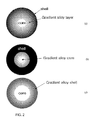
FIG. 2 , in a spherical nanocrystal structure of embodiments of the present invention, a corresponding alloy layer is shown in a gradient alloy structure, instead of a homogeneous alloy phase. See, for example,FIG. 2(a), (b), and (c) . -
FIG. 3 shows a structure of rod type interfused nanocrystals, according to embodiments of the present invention. In the generally two-dimensional shapes of rods, when two or more materials are longitudinally connected and grown, a first rod, an alloy interlayer, and a second rod may be sequentially formed. See, for example,FIG. 3(a) . In addition, the alloy interlayer may be in the form of a gradient alloy layer, instead of a homogenous alloy phase. See, for example,FIG. 3(b) . Even in the rod shape, when the two or more materials are longitudinally connected and grown, in the cases where the first rod is short or the second rod is more rapidly diffused into the first rod, the alloy layer may be diffused up to the end of the first rod, thereby forming an alloy rod-second rod structure. See, for example,FIG. 3(c) . -
FIG. 4 shows a structure of tripod type interfused nanocrystals, according to embodiments of the present invention. In the tripod shape, a first rod, a second rod, and a third rod may be radially formed around a core, and an alloy interlayer may be formed at the interface of the core and the three rods. See, for example,FIG. 4(a) . In addition, the alloy interlayer may be in the form of a gradient alloy layer, instead of a homogenous alloy phase. See, for example,FIG. 4(b) . In addition, when two or more materials are connected in a thickness direction to grow them, a core rod, an alloy interlayer, and a shell rod may be formed. -
FIG. 5 shows a structure of tube type interfused nanocrystals, according to embodiments of the present invention. In the three-dimensional shapes of tubes, a core , an alloy interlayer, and a shell may be sequentially formed. See, for example,FIG. 5(a) . In addition, the alloy interlayer may be in the form of a gradient alloy layer, instead of a homogenous alloy phase. See, for example,FIG. 5(b) . When two or more materials are connected in a thickness direction to grow them, in the cases where the core rod has a small diameter or the shell (or sheath) is thin, or either the shell or the core has a more rapid diffusion rate, an alloy core rod-shell structure or a core rodalloy shell structure may be formed by the diffusion of the alloy layer. - Specifically, as shown in
FIG. 1(a) , the interfused nanocrystals may include a core, an alloy interlayer, and a shell, each of which is sequentially formed. Because the shell material or core material may diffuse into the adjacent core material or shell material, respectively, the actual size of a core for light emission decreases, and thus, an emission wavelength may be shifted into the blue light range. Even if a core having a relatively large size is used, it may emit light in the blue light range. The shift of the emission wavelength may result from the chemical composition of the core for emission varying with diffusion of the shell material or core material into the adjacent core material or shell material, respectively. - In addition, in the case where the shell material has a wider band gap than the core, luminous efficiency in the blue light range may be drastically increased, by virtue of quantum confinement effects and passivation by the shell.
- The alloy layer, which may be formed on the outer surface of the core, functions to decrease the difference in a lattice constant between the core and the shell and thereby increase the material stability.
- Each of the materials constituting the nanocrystals of embodiments of the present invention may be selected from the group consisting of Group II-VI semiconductor compounds, Group III-V semiconductor compounds, Group IV-VI semiconductor compounds, and mixtures thereof.
- Specifically, materials constituting the nanocrystals may include, for example, CdS, CdSe, CdTe, ZnS, ZnSe, ZnTe, HgS, HgSe, HgTe, PbS, PbSe, PbTe, AIN, AIP, AlAs, GaN, GaP, GaAs, InN, InP, InAs, or mixtures thereof.
- The shape of each of the interfused nanocrystals according to embodiments of the present invention may be selected from the group consisting of spheres, tetrahedra, cylinders, rods, triangles, discs, tripods, tetrapods, cubes, boxes, stars, and tubes, but is not limited thereto.
- Below, the interfused nanocrystals according to embodiments of the present invention are represented by "CdSe//ZnS", which means a CdSe nanocrystal and a ZnS nanocrystal having an alloy interlayer therebetween.
- In addition, another aspect of embodiments of the present invention pertains to a method of preparing the interfused nanocrystals.
- That is, a method of preparing the interfused nanocrystals of embodiments of the present invention includes (a) forming a first nanocrystal, (b) growing a second nanocrystal comprising a material different from that of the first nanocrystal on the surface of the first nanocrystal obtained in (a), and (c) forming an alloy layer at an interface between the first nanocrystal and the second nanocrystal through diffusion.
- Specifically, in a preparation method of embodiments of the present invention, the formation of the first nanocrystal in (a) may be conducted by adding a metal precursor and a precursor of a Group V or VI compound to a solvent and a dispersant, and then mixing together to react. Likewise, the formation of the second nanocrystal in (b) may be conducted by adding metal precursor and a precursor of a Group V or VI compound to a solvent and a dispersant, and then mixing together to react and grow on the first nanocrystal.
- That is, the metal precursor and the precursor of a Group V or VI compound may be added to the solvent and the dispersant, and mixed together to react, to prepare a predetermined first nanocrystal. Subsequently, the first nanocrystal thus prepared may be added to a solution, containing precursors for a second nanocrystal in the solvent and the dispersant, and mixed together to react. Thereby, the second nanocrystal may be grown on the surface of the first nanocrystal, and the alloy interlayer may be formed at the interface between the first nanocrystal and the second nanocrystal through diffusion.
- The alloy interlayer may be formed at the interface between the first nanocrystal and the second nanocrystal, through diffusion of the second nanocrystal material into the first nanocrystal material, or of the first nanocrystal material into the second nanocrystal material. Therefore, as one nanocrystal material diffuses into the other nanocrystal material, the amount of the one nanocrystal material is reduced, thus obtaining nanocrystals having a new structure comprising an alloy interlayer formed at an interface between the first nanocrystal and the second nanocrystal. Such an alloy layer may decrease the difference in a lattice constant of the materials constituting the nanocrystals, therefore increasing the material stability. In addition, when the amount of the one nanocrystal material is reduced and then disappears, a first nanocrystal-alloy layer structure or an alloy layer-second nanocrystal structure may be formed.
- In a preparation method of embodiments of the present invention, (b) and (c) are repeatedly conducted once or more. In the core-shell structure, when the interfused nanocrystals obtained through (b) and (c) are subjected again to (b), the crystal growth reaction occurs on the surface of the second nanocrystal material to form another layer. In this regard, the rod structure may be formed into tripods or tetrapods.
- In a method of preparing the interfused nanocrystals of embodiments of the present invention, the metal precursor used in (a) and (b) may include, for example, dimethyl zinc, diethyl zinc, zinc acetate, zinc acetylacetonate, zinc iodide, zinc bromide, zinc chloride, zinc fluoride, zinc carbonate, zinc cyanide, zinc nitrate, zinc oxide, zinc peroxide, zinc perchlorate, zinc sulfate, dimethyl cadmium, diethyl cadmium, cadmium acetate, cadmium acetylacetonate, cadmium iodide, cadmium bromide, cadmium chloride, cadmium fluoride, cadmium carbonate, cadmium nitrate, cadmium oxide, cadmium perchlorate, cadmium phosphide, cadmium sulfate, mercury acetate, mercury iodide, mercury bromide, mercury chloride, mercury fluoride, mercury cyanide, mercury nitrate, mercury oxide, mercury perchlorate, mercury sulfate, lead acetate, lead bromide, lead chloride, lead fluoride, lead oxide, lead perchlorate, lead nitrate, lead sulfate, lead carbonate, tin acetate, tin bisacetylacetonate, tin bromide, tin chloride, tin fluoride, tin oxide, tin sulfate, germanium tetrachloride, germanium oxide, germanium ethoxide, gallium acetylacetonate, gallium chloride, gallium fluoride, gallium oxide, gallium nitrate, gallium sulfate, indium chloride, indium oxide, indium nitrate, or indium sulfate, but is not limited thereto.
- In addition, in a method of preparing the interfused nanocrystals of embodiments of the present invention, the Group V or VI compound used in (a) and (b) may include, for example, alkyl thiol compounds, such as hexanethiol, octanethiol, decanethiol, dodecanethiol, hexadecanethiol or mercaptopropylsilane, sulfur-trioctylphosphine (S-TOP), sulfur-tributylphosphine (S-TBP), sulfur-triphenylphosphine (S-TPP), sulfur-trioctylamine (S-TOA), trimethylsilyl sulfur, ammonium sulfide, sodium sulfide, selenium-trioctylphosphine (Se-TOP), selenium-tributylphosphine (Se-TBP), selenium-triphenylphosphine (Se-TPP), tellurium-trioctylphosphine (Te-TOP), tellurium-tributylphosphine (Te-TBP), tellurium-triphenylphosphine (Te-TPP), trimethylsilyl phosphine, alkyl phosphines, such as triethyl phosphine, tributyl phosphine, tri octyl phosphine, triphenyl phosphine or tricyclohexyl phosphine, arsenic oxide, arsenic chloride, arsenic sulfate, arsenic bromide, arsenic iodide, nitric oxide, nitric acid, ammonium nitrate, etc.
- As such, it is preferable that the concentration and rate of addition of the precursor be appropriately controlled depending on the reactivity of the precursor, so that undesired side-reactions, such as the separation of metal in the form of particles or the formation of additional particles by the reaction between the metal and the precursor of the Group V or VI compound, do not occur.
- In addition, in a method of preparing the interfused nanocrystals of embodiments of the present invention, the solvent used in (a) and (b) may include, for example, primary alkyl amines having 6 to 22 carbons, secondary alkyl amines having 6 to 22 carbons, and tertiary alkyl amines having 6 to 22 carbons; primary alcohols having 6 to 22 carbons, secondary alcohols having 6 to 22 carbons, and tertiary alcohols having 6 to 22 carbons; ketones and esters, either of which have 6 to 22 carbons; a heterocyclic compound including nitrogen or sulfur, which has 6 to 22 carbons; alkanes having 6 to 22 carbons, alkenes having 6 to 22 carbons, and alkynes having 6 to 22 carbons; trioctylphosphine; and trioctylphosphine oxide.
- In addition, in a method of preparing the interfused nanocrystals of embodiments of the present invention, the dispersant used in (a) and (b) may include, for example, alkanes or alkenes having 6 to 22 carbons and a COOH group at a terminal end thereof; alkanes or alkenes having 6 to 22 carbons and a POOH group at a terminal end thereof; alkanes or alkenes having 6 to 22 carbons and an SOOH group at a terminal end thereof; or alkanes or alkenes having 6 to 22 carbons and an NH2 group at a terminal end thereof.
- Specifically, the dispersant is exemplified by, but not limited to, oleic acid, stearic acid, palmitic acid, hexyl phosphonic acid, n-octyl phosphonic acid, tetradecyl phosphonic acid, octadecyl phosphonic acid, n-octyl amine, and hexadecyl amine.
- In addition, in a method of preparing the interfused nanocrystals of embodiments of the present invention, (a) and (b) may each be conducted at 100°C to 460°C, preferably 120°C to 390°C, and more preferably 150°C to 360°C, to assure the stability of the solvent while easily growing the crystals.
- In addition, in a method of preparing the interfused nanocrystals of embodiments of the present invention, (a) and (b) may each be conducted for a time period from 5 sec to 4 hr, preferably from 10 sec to 3 hr, and more preferably, from 20 sec to 2 hr, to easily control the reaction rate.
- In addition, in a method of preparing the interfused nanocrystals of embodiments of the present invention, the diffusion rate in (c) may be controlled by varying the reaction temperature, the reaction time, and the concentration of the metal precursor of the second nanocrystal in (b). Thus, even if a first nanocrystal having a consistent size is used, a material having a different emission wavelength may be obtained. By the same principle, even if a first nanocrystal having a varying size is used, the diffusion rate is controlled, therefore obtaining a material emitting light at a same wavelength.
- Further, the diffusion rate in (c) may be controlled by stepwisely varying the reaction temperature in (b). Hence, even if a first nanocrystal having a consistent size is used, a material having a different emission wavelength may be obtained.
- In addition, in a method of preparing the interfused nanocrystals of embodiments of the present invention, the metal precursor used in (b) may have a concentration of 0.001 M to 2 M, and preferably 0.1 M to 1.6 M, to increase the luminous efficiency in the blue light wavelength range.
- In addition, in a method of preparing the interfused nanocrystals of embodiments of the present invention, the molar ratio of a metal precursor to a precursor of a Group V or VI compound used in (b) may range from 100:1 to 1:50, and preferably from 50:1 to 1:10, to increase the luminous efficiency in the blue light wavelength range.
- A further aspect of embodiments of the present invention pertains to interfused nanocrystals prepared using the above method. The shape of each of the nanocrystals may be selected from the group consisting of spheres, tetrahedra, cylinders, rods, triangles, discs, tripods, tetrapods, cubes, boxes, stars, and tubes, but is not limited thereto.
- The above nanocrystals may have an emission range from 350 nm to 700 nm, and preferably, from 380 nm to 490 nm and emit light with a maximum emission peak in the above range. The quantum efficiency of the nanocrystals is in the range of 0.1 % to 100%, and preferably, 20% to 100%.
- Interfused nanocrystals of embodiments of the present invention may be variously applied to displays, sensors, energy fields, etc., and, in particular, are useful in the formation of the light-emitting layer of a light-emitting diode for emitting blue light.
- Yet another aspect of embodiments of the present invention pertains to a diode including the interfused nanocrystals. Specifically, an organic-inorganic electrical light-emitting diode, in which the interfused nanocrystals are used as a light-emitting layer, may be provided.
- As is apparent from
FIG. 12 , an organic-inorganic electrical light-emitting diode of embodiments of the present invention may comprise asubstrate 10, a hole-injectingelectrode 20, a hole-transporting layer 30, a light-emitting layer 40, an electron-transportinglayer 50, and an electron-injectinglayer 60, each of which is sequentially formed. The light-emitting layer 40 may include interfused semiconductor nanocrystals of embodiments of the present invention. - Hole-transporting layer 30 and light-emitting layer 40 may be formed as a single layer. Also, electron-injecting
layer 60 may be formed of two or more layers. - Further, in embodiments of the present invention, a hole-inhibiting
layer 70 may be selectively formed between the light-emitting layer 40 and the electron-transportinglayer 50. - Specifically, the
substrate 10 used in the electrical light-emitting diode of embodiments of the present invention may include commonly used substrates, for example, a glass substrate or a transparent plastic substrate, having excellent transparency, surface evenness, ease of handling and waterproofness. More particularly, it is exemplified by a glass substrate, a polyethyleneterephthalate substrate, or a polycarbonate substrate. - In addition, a material for the hole-injecting
electrode 20 may include conductive metals or oxides thereof, for example, ITO (Indium Tin Oxide), IZO (Indium Zinc Oxide), nickel (Ni), platinum (Pt), gold (Au), silver (Ag), iridium (Ir). - In addition, a material for the hole-transporting layer 30 may include all commonly used materials, for example, poly(3,4-ethylenediophene) (PEDOT)/polystyrene p-sulfonate (PSS), poly-N-vinylcarbazole derivatives, polyphenylenevinylene derivatives, polyparaphenylene derivatives, polymethacrylate derivatives, poly(9,9-octylfluorene) derivatives, poly(spiro-fluorene) derivatives, or TPD (N,N'-bis-(3-methylphenyl)-N,N'-bis-(phenyl)-benzidine), but is not limited thereto. The hole-transporting layer 30 of embodiments of the present invention is preferably 10 to 100 nm thick.
- In addition, a material for the electron-transporting
layer 50 may include commonly used materials, for example, an oxazole compound, an iso-oxazole compound, a triazole compound, an iso-thiazole compound, an oxydiazole compound, a thiadiazole compound, a perylene compound, an aluminum complex, such as tris(8-hydroxyquinoline)-aluminum (Alq3), bis(2-methyl-8-quinolato)(p-phenylphenolato)aluminum (Balq), bis(2-methyl-8-quinolinato)(triphenylsiloxy)aluminum(III) (Salq), but is not limited thereto. In embodiments of the present invention, the electron-transportinglayer 50 is preferably 10 to 100 nm thick. - In addition, a material for the electron-injecting
electrode 60 may include metals having a low work function to easily inject an electron, for example, I, Ca, Ba, Ca/Al, LiF/Ca, LiF/Al, BaF2/Al, BaF2/Ca/Al, Al, Mg, Ag:Mg alloy, but is not limited thereto. In embodiments of the present invention, the electron-injectingelectrode 60 is preferably 50 to 300 nm thick. - Further, a material for the hole-inhibiting
layer 70 may include materials commonly used in the art, for example, 3-(4-biphenylyl)-4-phenyl-5-(4-tert-butylphenyl)-1,2,4-triazole (TAZ), 2,9-dimethyl-1,10-phenanthroline (BCP), a phenanthroline compound, an imidazole compound, a triazole compound, an oxadiazole compound, an aluminum complex, but is not limited thereto. In embodiments of the present invention, the hole-inhibitinglayer 70 is preferably 5 to 50 nm thick. - A better understanding of embodiments of the present invention may be obtained in light of the following examples, which are set forth to illustrate, but are not to be construed to limit embodiments of the present invention.
- 16 g of trioctylamine (TOA), 0.3 g of octadecyl phosphonic acid, and 0.4 mmol cadmium oxide were simultaneously loaded into a 125 ml flask equipped with a reflux condenser, and then the temperature of the reaction mixture was maintained at 300°C with stirring. Separately, a 2 M Se-TOP solution was prepared by dissolving Se powder in trioctylphosphine (TOP). 2 ml of the 2 M Se-TOP solution was rapidly added to the above stirred reaction mixture, and reacted for about 2 min. After completion of the reaction, the reaction mixture was cooled down to room temperature rapidly, and ethanol was added as a non-solvent. After centrifuging the obtained reaction solution, the supernatant of the solution was decanted, with the exception of the centrifuged precipitate, and the precipitate was dispersed in toluene, to prepare a CdSe nanocrystal solution.
- 8 g of TOA, 0.1 g of oleic acid, and 0.4 mmol zinc acetate were simultaneously loaded into a 125 ml flask equipped with a reflux condenser, and the reaction temperature was maintained at 300°C with stirring. Subsequently, the above-synthesized CdSe nanocrystal solution was added to the reaction mixture, and an S-TOP solution was slowly added. The reaction was performed for about 1 hr. After completion of the reaction, the reaction mixture was cooled down to room temperature rapidly, and ethanol was added as a non-solvent. After centrifuging the obtained reaction solution, the supernatant of the solution was decanted, with the exception of the centrifuged precipitate, and the precipitate was dispersed in toluene, to prepare CdSe//ZnS as interfused nanocrystals having a size of 5 nm.
- The nanocrystals thus obtained emitted blue light under a 365 nm UV lamp. The transmission electron micrograph of the interfused CdSe core and the CdSe//ZnS nanocrystals is shown in
FIG. 6 andFIG. 7 , respectively. A photoluminescence spectra, showing the excited light emission spectrum of the CdSe nad the CdSe//ZnS nanocrystals, is shown inFIG. 8 . As shown inFIG. 3 , maximum emission peaks of the interfused CdSe//ZnS nanocrystals and the CdSe core appeared at 470 nm and 496 nm, respectively. - 8 g of TOA, 0.1 g of oleic acid, and 0.4 mmol zinc acetate were simultaneously loaded into a 125 ml flask equipped with a reflux condenser, and the temperature of the reaction mixture was maintained at each of 220, 260, 300 and 320°C with stirring. Subsequently, the CdSe nanocrystal solution synthesized in Example 1 was added to the reaction mixture, and an S-TOP solution was slowly added thereto. The reaction was performed for about 1 hr. After completion of the reaction, the reaction mixture was cooled down to room temperature rapidly, and ethanol was added as a non-solvent. After centrifuging the obtained reaction solution, the supernatant of the solution was decanted, with the exception of the centrifuged precipitate, and the precipitate was dispersed in toluene, to prepare CdSe//ZnS as interfused nanocrystals having a size of 5 nm.
- The CdSe core had a maximum emission peak of 522 nm, and the interfused CdSe//ZnS nanocrystals emitted blue light at a wavelength that varied with the reaction temperature. The variation in emission peaks depending on the reaction temperature is summarized in Table 1, below.
Table 1 Emission Wavelength of CdSe/Zns Synthesized at Different Reaction Temperatures using CdSe Core Emitting Light at 522 nm Reaction Temperature (°C) Emission Wavelength (nm) 220 498 260 476 300 440 320 442 - 8 g of TOA, 0.1 g of oleic acid, and 0.4 mmol zinc acetate were simultaneously loaded into a 125 ml flask equipped with a reflux condenser, and the temperature of the reaction mixture was maintained at 300°C with stirring. Subsequently, the CdSe nanocrystal solution synthesized in Example 1 was added to the reaction mixture, and an S-TOP solution was slowly added thereto. The reaction was performed for each of 5 min, 20 min, 40 min, and 1 hr. After completion of the reaction, the reaction mixture was cooled down to room temperature rapidly, and ethanol was added as a non-solvent. After centrifuging the obtained reaction solution, the supernatant of the solution was decanted, with the exception of the centrifuged precipitate, and the precipitate was dispersed in toluene, to prepare CdSe//ZnS as interfused nanocrystals having a size of 5 nm.
- The nanocrystals thus obtained emitted blue light under a 365 nm UV lamp. The CdSe core had a maximum emission peak of 496 nm, and the interfused CdSe//ZnS nanocrystals emitted blue light at a wavelength that varied with the reaction time. The variation in emission peaks depending on the reaction time is summarized in Table 2, below.
Table 2 Emission Wavelength of CdSe//ZnS Synthesized for Different Reaction Times using CdSe Core Emitting Light at 496 nm Reaction Time (min) Emission Wavelength (nm) 0 496 5 484 20 476 40 464 60 440 - Into a 125 ml flask equipped with a reflux condenser, 8 g of TOA was loaded while oleic acid was added in varying amounts of 0.01, 0.05, and 0.1 g and zinc acetate in varying concentrations of 0.04, 0.2 and 0.4 mmol. The temperature of the reaction mixture was maintained at 300°C with stirring. Subsequently, the CdSe nanocrystal solution synthesized in Example 1 was added to the reaction mixture, and an S-TOP solution was slowly added thereto. The reaction was performed for about 30 min. After completion of the reaction, the reaction mixture was cooled down to room temperature rapidly, and ethanol was added as a non-solvent. After centrifuging the obtained reaction solution, the supernatant of the solution was decanted, with the exception of the centrifuged precipitate, and the precipitate was dispersed in toluene, to prepare CdSe//ZnS as interfused nanocrystals having a size of 5 nm.
- The CdSe core had a maximum emission peak of 496 nm, and the interfused CdSe//ZnS nanocrystals emitted blue light at a wavelength that varied with the concentration of the precursor. The variation in emission peaks depending on the concentration of the precursor is summarized in Table 3, below.
Table 3 Emission Wavelength of CdSe/rZns Synthesized at Different Precursor Concentrations for 30 min using CdSe Core Emitting Light at 496 nm Concentration of Zn Precursor in Synthesized Solution (mM) Emission Wavelength (nm) 4 474 20 468 40 459 - 16 g of TOA, 0.3 g of octadecyl phosphonic acid, and 0.4 mmol cadmium oxide were simultaneously loaded into a 125 ml flask equipped with a reflux condenser, and then the temperature of the reaction mixture was maintained at 300°C with stirring. Separately, a 2 M Se-TOP solution was prepared by dissolving Se powder in trioctylphosphine (TOP). 2 ml of the 2 M Se-TOP complex solution was rapidly added to the above stirred reaction mixture, and the reaction was performed for about 2 min. After completion of the reaction, the reaction mixture was cooled down to room temperature rapidly, and ethanol was added as a non-solvent. After centrifuging the obtained reaction solution, the supernatant of the solution was decanted, with the exception of the centrifuged precipitate, and the precipitate was dispersed in toluene, to prepare a CdSe nanocrystal solution.
- 8 g of TOA, 0.1 g of oleic acid, and 0.4 mmol zinc acetate were simultaneously loaded into a 125 ml flask equipped with a reflux condenser, and the temperature of the reaction mixture was maintained at 260°C with stirring. Subsequently, the above-synthesized CdSe nanocrystal solution was added to the reaction mixture, and an S-TOP solution was slowly added thereto. The reaction was performed for about 1 hr. Thereafter, the reaction temperature was slowly increased to 300°C, at which the reaction performed for about 1 hr. After completion of the reaction, the reaction mixture was cooled down to room temperature rapidly, and ethanol was added as a non-solvent. After centrifuging the obtained reaction solution, the supernatant of the solution was decanted, with the exception of the centrifuged precipitate, and the precipitate was dispersed in toluene, to prepare CdSe//ZnS as interfused nanocrystals having a size of 5 nm.
- A photoluminescence spectra, showing the excited light emission spectrum of the CdSe solution used as a core, the nanocrystal solution obtained through the reaction at 260°C for 1 hr, and the nanocrystal solution obtained through the reaction at 260°C for 1 hr and then 300°C for 1 hr, is shown in
FIG. 9 . As shown inFIG. 9 , maximum emission peaks appeared at 498, 492 and 466 nm, respectively. - 8 g of TOA, 0.1 g of oleic acid, and 0.4 mmol zinc acetate were simultaneously loaded into a 125 ml flask equipped with a reflux condenser, and the temperature of the reaction mixture was maintained at 300°C with stirring. Subsequently, the CdSe nanocrystal solution synthesized in Example 1 was added to the reaction mixture, and a Se-TOP complex solution was slowly added thereto. The reaction occurred for about 1 hr. After completion of the reaction, the reaction mixture was cooled down to room temperature rapidly, and ethanol was added as a non-solvent. After centrifuging the obtained reaction solution, the supernatant of the solution was decanted, with the exception of the centrifuged precipitate, and the precipitate was dispersed in toluene, to prepare CdSe//ZnSe as interfused nanocrystals having a size of 5 nm.
- The nanocrystals thus obtained emitted blue light under a 365 nm UV lamp. A photoluminescence spectra, showing the excited light emission spectrum of the above nanocrystal solution and the CdSe core, is shown in
FIG. 10 . As shown inFIG. 10 , maximum emission peaks appeared at 472 nm and 496 nm, respectively. - 16 g of TOA, 0.5 g of oleic acid, and 0.4 mmol cadmium oxide were simultaneously loaded into a 125 ml flask equipped with a reflux condenser, and then the reaction temperature was maintained at 300°C while the reaction mixture was stirred. Separately, a 0.25 M Se-TOP solution was prepared by dissolving Se powder in trioctylphosphine (TOP), and a 1.0 M S-TOP solution was prepared by dissolving S powder in trioctylphosphine (TOP). A mixture of 0.9 ml of the S-TOP solution and 0.1 ml of the Se-TOP solution were rapidly added to the above stirred reaction mixture, and further reacted for 4 min. After completion of the reaction, the reaction mixture was cooled down to room temperature rapidly, and ethanol was added as a non-solvent. After centrifuging the obtained reaction solution, the supernatant of the solution was decanted, with the exception of the centrifuged precipitate, and the precipitate was dispersed in toluene to obtain a 1 wt% solution, to prepare a CdSeS nanocrystal solution.
- 8 g of TOA, 0.1 g of oleic acid, and 0.4 mmol zinc acetate were simultaneously loaded into a 125 ml flask equipped with a reflux condenser, and the temperature of the reaction mixture was maintained at 300°C with stirring. Subsequently, the above synthesized CdSeS nanocrystal solution was added to the reaction mixture, and the S-TOP solution was slowly added thereto. The reaction was performed for about 1 hr. After completion of the reaction, the reaction mixture was cooled down to room temperature rapidly, and ethanol was added as a non-solvent. After centrifuging the obtained reaction solution, the supernatant of the solution was decanted, with the exception of the centrifuged precipitate, and the precipitate was dispersed in toluene, to prepare CdSeS//ZnS as interfused nanocrystals having a size of 5 nm.
- The nanocrystals thus obtained emitted blue light under a 365 nm UV lamp. A photoluminescence spectrum, showing the excited light emission spectrum of the above nanocrystal solution and the CdSeS core, is shown in
FIG. 11 . As is apparent fromFIG. 11 , maximum emission peaks appeared at 527 nm and 540 nm, respectively. - The present example is a preparative example of manufacturing an organic-inorganic hybrid electrical light emitting diode using the CdSe//ZnS nanocrystals prepared in Example 1 as a light emitting material of the electrical light emitting diode.
- A chloroform solution of 3 wt% N,N'-bis-(3-methylphenyl)-N,N'-bis-(phenyl)-benzidine (TPD) serving as a hole transporting material and a chloroform solution of 1 wt% CdSe//ZnS prepared in Example 1 were mixed and spin-coated on a patterned ITO layer, and then dried, to form a single hole transporting and light emitting layer.
- On the completely dried hole transporting and light emitting layer formed of nanocrystals, 3-(4-biphenylyl)-4-phenyl-5-(4-tert-butylphenyl)-1,2,4-triazole (TAZ) was deposited to a thickness of 10 nm, to form a hole inhibiting layer, on which tris-(8-hydroxyquinoline)aluminum (Alq3) serving as an electron transporting layer was deposited to a thickness of 30 nm. Subsequently, LiF was deposited to a thickness of 1 nm on the electron transporting layer, after which aluminum was deposited to a thickness of 200 nm to form a cathode, thereby completing an electrical light emitting diode.
- The structure of the organic-inorganic hybrid electrical light emitting diode thus manufactured is shown in
FIG. 12 , and the electrical light emitting spectrum thereof is shown inFIG. 13 . As is apparent fromFIG. 13 , the emission peak was about 470 nm, FWHM was about 36 nm, and brightness was 500 Cd/m2, and the efficiency of the device was 1.5 Cd/A. - As described hereinbefore, embodiments of the present invention provide interfused nanocrystals and a method of preparing the interfused nanocrystals. Interfused nanocrystals of embodiments of the present invention have an alloy layer between different crystals, thus increasing the material stability. Further, material having very excellent light emitting efficiency in the blue light range may be prepared.
- Various aspects of the present invention may be summarized by the following numbered paragraphs:
- 1. Interfused nanocrystals, comprising two or more materials, in which an alloy layer formed of the two or more materials is included.
- 2. The nanocrystals of
paragraph 1, wherein the alloy layer is an alloy interlayer formed at an interface between the two or more materials. - 3. The nanocrystals of
paragraph 1 or 2, wherein the alloy layer is a gradient alloy layer. - 4. The nanocrystals of paragraph claim 3, wherein one of the two or more materials is subsumed into the gradient alloy layer.
- 5. The nanocrystals of any of
paragraphs 1 to 4, wherein the alloy layer is an alloy layer formed from diffusion of a first material into a second material. - 6. The nanocrystals of any of
paragraphs 1 to 5, wherein each of the materials constituting the nanocrystals is, independently, selected from Group II-VI semiconductor compounds, Group III-V semiconductor compounds, Group IV-VI semiconductor compounds, and mixtures thereof. - 7. The nanocrystals of any of
paragraphs 1 to 5, wherein each of the materials constituting the nanocrystals is, independently, selected from CdS, CdSe, CdTe, ZnS, ZnSe, ZnTe, HgS, HgSe, HgTe, PbS, PbSe, PbTe, AIN, AIP, AlAs, GaN, GaP, GaAs, InN, InP, InAs, and mixtures thereof. - 8. The nanocrystals of any of
paragraphs 1 to 7, wherein a shape of each of the nanocrystals is selected from the group consisting of spheres, tetrahedra, cylinders, rods, triangles, discs, tripods, tetrapods, cubes, boxes, stars, and tubes. - 9. A method of preparing interfused nanocrystals, comprising:
- (a) forming a first nanocrystal;
- (b) growing a second nanocrystal comprising a material different from that of the first nanocrystal on a surface of the first nanocrystal formed in (a); and
- (c) forming an alloy layer at an interface between the first nanocrystal and the second nanocrystal through diffusion.
- 10. The method of paragraph 9, wherein (b) and (c) are conducted multiple times.
- 11. The method of
paragraph 9 or 10, wherein the forming of the first nanocrystal in (a) is conducted by adding a metal precursor and a precursor of a Group V or VI compound to a solvent and a dispersant, and then mixing together to react, and, wherein the forming of the second nanocrystal in (b) is conducted by adding a metal precursor and a precursor of a Group V or VI compound to a solvent and a dispersant, and then mixing together to react. - 12. The method of any of paragraphs 9 to 11, wherein the first nanocrystals are formed by adding a metal precursor and a precursor of a Group V or VI compound to a first solvent and a first dispersant, and then mixing together to react, and
wherein growing a second nanocrystal on a surface of the first nanocrystal comprises adding the first nanocrystal thus prepared to a solution containing precursors for a second nanocrystal in a second solvent and a second dispersant, and then mixing together to react. - 13. The method of any of paragraphs 9 to 12, wherein the alloy layer is an alloy interlayer comprising an alloy of the first nanocrystal and the second nanocrystal and being formed at the interface between the first nanocrystal and the second nanocrystal.
- 14. The method of any of paragraphs 9 to 13, wherein the alloy layer is a gradient alloy layer comprising an alloy of the first nanocrystal and the second nanocrystal.
- 15. The method of any of paragraphs 9 to 14, wherein the alloy layer is an alloy layer formed from diffusion of the second nanocrystal material into the first nanocrystal material.
- 16. The method of paragraph 15, wherein the first nanocrystal material is subsumed into the alloy layer.
- 17. The method of any of paragraphs 9 to 16, wherein the alloy layer is an alloy layer formed from diffusion of the first nanocrystal material into the second nanocrystal material.
- 18. The method of paragraph 17, wherein the second nanocrystal material is subsumed into the alloy layer.
- 19. The method of any of paragraphs 11 to 18, wherein the metal precursor is selected from dimethyl zinc, diethyl zinc, zinc acetate, zinc acetylacetonate, zinc iodide, zinc bromide, zinc chloride, zinc fluoride, zinc carbonate, zinc cyanide, zinc nitrate, zinc oxide, zinc peroxide, zinc perchlorate, zinc sulfate, dimethyl cadmium, diethyl cadmium, cadmium acetate, cadmium acetylacetonate, cadmium iodide, cadmium bromide, cadmium chloride, cadmium fluoride, cadmium carbonate, cadmium nitrate, cadmium oxide, cadmium perchlorate, cadmium phosphide, cadmium sulfate, mercury acetate, mercury iodide, mercury bromide, mercury chloride, mercury fluoride, mercury cyanide, mercury nitrate, mercury oxide, mercury perchlorate, mercury sulfate, lead acetate, lead bromide, lead chloride, lead fluoride, lead oxide, lead perchlorate, lead nitrate, lead sulfate, lead carbonate, tin acetate, tin bisacetylacetonate, tin bromide, tin chloride, tin fluoride, tin oxide, tin sulfate, germanium tetrachloride, germanium oxide, germanium ethoxide, gallium acetylacetonate, gallium chloride, gallium fluoride, gallium oxide, gallium nitrate, gallium sulfate, indium chloride, indium oxide, indium nitrate, and indium sulfate.
- 20. The method of any of paragraphs 11 to 19, wherein the Group V or VI compound is selected from alkyl thiol compounds, including hexanethiol, octanethiol, decanethiol, dodecanethiol, hexadecanethiol or mercaptopropylsilane, sulfur-trioctylphosphine (S-TOP), sulfur-tributylphosphine (S-TBP), sulfur-triphenylphosphine (S-TPP), sulfur-trioctylamine (S-TOA), trimethylsilyl sulfur, ammonium sulfide, sodium sulfide, selenium-trioctylphosphine (Se-TOP), selenium-tributylphosphine (Se-TBP), selenium-triphenylphosphine (Se-TPP), tellurium-trioctylphosphine (Te-TOP), tellurium-tributylphosphine (Te-TBP), tellurium-triphenylphosphine (Te-TPP), trimethylsilyl phosphine, alkyl phosphines, including triethyl phosphine, tributyl phosphine, trioctyl phosphine, triphenyl phosphine or tricyclohexyl phosphine, arsenic oxide, arsenic chloride, arsenic sulfate, arsenic bromide, arsenic iodide, nitric oxide, nitric acid, and ammonium nitrate.
- 21. The method of any of paragraphs 11 to 20, wherein the solvent is selected from primary alkyl amines, secondary alkyl amines, and tertiary alkyl amines, each of which has 6 to 22 carbons; primary alcohols, secondary alcohols, and tertiary alcohols, each of which has 6 to 22 carbons; ketones and esters, either of which have 6 to 22 carbons; a heterocyclic compound including nitrogen or sulfur, which has 6 to 22 carbons; alkanes, alkenes, and alkynes, each of which has 6 to 22 carbons; trioctylphosphine; and trioctylphosphine oxide.
- 22. The method of any of paragraphs 11 to 21, wherein the dispersant is selected from alkanes or alkenes having 6 to 22 carbons and a carboxylic acid functional group at a terminal end thereof, alkanes or alkenes having 6 to 22 carbons and a phosphonic acid functional group at a terminal end thereof, alkanes or alkenes having 6 to 22 carbons and a sulfonic acid functional group at a terminal end thereof, and alkanes or alkenes having 6 to 22 carbons and an amine (-NH2) group at a terminal end thereof.
- 23. The method of any of paragraphs 11 to 22, wherein the dispersant is selected from oleic acid, stearic acid, palmitic acid, hexyl phosphonic acid, n-octyl phosphonic acid, tetradecyl phosphonic acid, octadecyl phosphonic acid, n-octyl amine, and hexadecyl amine.
- 24. The method of any of paragraphs 9 to 23, wherein each of (a) and (b) is conducted at 100°C to 460°C.
- 25. The method of any of paragraphs 9 to 24, wherein each of (a) and (b) is conducted for a time period from 5 sec to 4 hr.
- 26. The method of any of paragraphs 9 to 25, wherein the reaction temperature of (b) increases or decreases stepwisely.
- 27. The method of any of paragraphs 9 to 26, wherein the metal precursor used in (b) has a concentration of 0.001 M to 2 M.
- 28. The method of any of paragraphs 9 to 27, wherein a molar ratio of the metal precursor to the precursor of a Group V or VI compound used in (b) ranges from 100:1 to 1:50.
- 29. The method of any of paragraphs 9 to 28, wherein the nanocrystals are formed in the shape of spheres, tetrahedra, cylinders, rods, triangles, discs, tripods, tetrapods, cubes, boxes, stars or tubes.
- 30. The method of any of paragraphs 9 to 29, wherein the nanocrystals have a maximum emission peak in a range of 350 nm to 700 nm and quantum efficiency of 0.1% to 100%.
- 31. A diode, comprising the interfused nanocrystals prepared by the method of any of paragraphs 9 to claim 30.
- 32. The diode of paragraph 31, wherein the diode is an organic-inorganic hybrid electrical light-emitting diode.
- 33. The diode of paragraph 32, wherein the organic-inorganic hybrid electrical light-emitting diode comprises:
- (i) a substrate;
- (ii) a hole-injecting electrode;
- (iii) a hole-transporting and light-emitting layer;
- (iv) an electron-transporting layer; and
- (v) an electron-injecting electrode,
wherein the light-emitting layer includes the interfused semiconductor nanocrystals. - 34. The diode of paragraph 32, wherein the organic-inorganic hybrid electrical light-emitting diode comprises:
- (i) a substrate;
- (ii) a hole-injecting electrode;
- (iii) a hole-transporting layer;
- (iv) a light-emitting layer;
- (v) an electron-transporting layer; and
- (vi) an electron-injecting electrode,
wherein the light-emitting layer includes the interfused semiconductor nanocrystals. - 35. The diode of paragraph 34, further comprising a hole-inhibiting layer between the light-emitting layer and the electron-transporting layer.
- 36. The diode of paragraph 34 or 35, wherein the substrate is selected from a glass substrate, a polyethyleneterephthalate substrate, and a polycarbonate substrate.
- 37. The diode of any of paragraphs 33 to 36, wherein the hole-injecting electrode comprises a material selected from the group consisting of conductive metals and oxides thereof, including ITO (Indium Tin Oxide), IZO (Indium Zinc Oxide), nickel (Ni), platinum (Pt), gold (Au), silver (Ag), or iridium (Ir).
- 38. The diode of any of paragraphs 33 to 37, wherein the hole-transporting layer comprises a material selected from poly(3,4-ethylenediophene) (PEDOT)/polystyrene p-sulfonate (PSS), poly-N-vinylcarbazole derivatives, polyphenylenevinylene derivatives, polyparaphenylene derivatives, polymethacrylate derivatives, poly(9,9-octylfluorene) derivatives, poly(spiro-fluorene) derivatives, or TPD (N,N'-bis-(3-methylphenyl)-N,N'-bis-(phenyl)-benzidine).
- 39. The diode of any of paragraphs 34 to 38, wherein the electron-transporting layer comprises a material selected from an oxazole compound, an iso-oxazole compound, a triazole compound, an iso-thiazole compound, an oxydiazole compound, a thiadiazole compound, a perylene compound, and an aluminum complex, including tris(8-hydroxyquinoline)-aluminum (Alq3), bis(2-methyl-8-quinolato)(p-phenylphenolato)aluminum (Balq) or bis(2-methyl-8-quinolinato)(triphenylsiloxy)aluminum(III) (Salq).
- 40. The diode of any of paragraphs 33 to 39, wherein the electron-injecting electrode comprises a material selected from I, Ca, Ba, Ca/Al, LiF/Ca, LiF/Al, BaF2/Al, BaF2/Ca/Al, Al, Mg, and Ag:Mg alloy.
- 41. The diode of any of paragraphs 35 to 40, wherein the hole-inhibiting layer comprises a material selected from 3-(4-biphenylyl)-4-phenyl-5-(4-tert-butylphenyl)-1,2,4-triazole (TAZ), 2,9-dimethyl-1,10-phenanthroline (BCP), a phenanthroline compound, an imidazole compound, a triazole compound, an oxadiazole compound, and an aluminum complex.
Claims (15)
- A method of preparing interfused nanocrystals, comprising:(a) forming a first nanocrystal;(b) growing a second nanocrystal comprising a material different from that of the first nanocrystal on a surface of the first nanocrystal formed in (a); and(c) forming an alloy layer at an interface between the first nanocrystal and the second nanocrystal through diffusion.
- The method as claimed in claim 1, wherein (b) and (c) are conducted multiple times.
- The method as claimed in claim 1 or 2, wherein the forming of the first nanocrystal in (a) is conducted by adding a metal precursor and a precursor of a Group V or VI compound to a solvent and a dispersant, and then mixing together to react, and, wherein the forming of the second nanocrystal in (b) is conducted by adding a metal precursor and a precursor of a Group V or VI compound to a solvent and a dispersant, and then mixing together to react.
- The method as claimed in any of claims 1 to 3, wherein the first nanocrystals are formed by adding a metal precursor and a precursor of a Group V or VI compound to a first solvent and a first dispersant, and then mixing together to react, and
wherein growing a second nanocrystal on a surface of the first nanocrystal comprises adding the first nanocrystal thus prepared to a solution containing precursors for a second nanocrystal in a second solvent and a second dispersant, and then mixing together to react. - The method as claimed in any of claims 1 to 4, wherein the alloy layer is an alloy interlayer comprising an alloy of the first nanocrystal and the second nanocrystal and being formed at the interface between the first nanocrystal and the second nanocrystal.
- The method as claimed in any of claims 1 to 5, wherein the alloy layer is a gradient alloy layer comprising an alloy of the first nanocrystal and the second nanocrystal.
- The method as claimed in any of claims 1 to 6, wherein the alloy layer is an alloy layer formed from diffusion of the second nanocrystal material into the first nanocrystal material or from diffusion of the first nanocrystal material into the second nanocrystal material.
- The method as claimed in any of claims 1 to 7, wherein the metal precursor is selected from dimethyl zinc, diethyl zinc, zinc acetate, zinc acetylacetonate, zinc iodide, zinc bromide, zinc chloride, zinc fluoride, zinc carbonate, zinc cyanide, zinc nitrate, zinc oxide, zinc peroxide, zinc perchlorate, zinc sulfate, dimethyl cadmium, diethyl cadmium, cadmium acetate, cadmium acetylacetonate, cadmium iodide, cadmium bromide, cadmium chloride, cadmium fluoride, cadmium carbonate, cadmium nitrate, cadmium oxide, cadmium perchlorate, cadmium phosphide, cadmium sulfate, mercury acetate, mercury iodide, mercury bromide, mercury chloride, mercury fluoride, mercury cyanide, mercury nitrate, mercury oxide, mercury perchlorate, mercury sulfate, lead acetate, lead bromide, lead chloride, lead fluoride, lead oxide, lead perchlorate, lead nitrate, lead sulfate, lead carbonate, tin acetate, tin bisacetylacetonate, tin bromide, tin chloride, tin fluoride, tin oxide, tin sulfate, germanium tetrachloride, germanium oxide, germanium ethoxide, gallium acetylacetonate, gallium chloride, gallium fluoride, gallium oxide, gallium nitrate, gallium sulfate, indium chloride, indium oxide, indium nitrate, and indium sulfate, and/or
wherein the Group V or VI compound is selected from alkyl thiol compounds, including hexanethiol, octanethiol, decanethiol, dodecanethiol, hexadecanethiol or mercaptopropylsilane, sulfur-trioctylphosphine (S-TOP), sulfur-tributylphosphine (S-TBP), sulfur-triphenylphosphine (S-TPP), sulfur-trioctylamine (S-TOA), trimethylsilyl sulfur, ammonium sulfide, sodium sulfide, selenium-trioctylphosphine (Se-TOP), selenium-tributylphosphine (Se-TBP), selenium-triphenylphosphine (Se-TPP), tellurium-trioctylphosphine (Te-TOP), tellurium-tributylphosphine (Te-TBP), tellurium-triphenylphosphine (Te-TPP), trimethylsilyl phosphine, alkyl phosphines, including triethyl phosphine, tributyl phosphine, trioctyl phosphine, triphenyl phosphine or tricyclohexyl phosphine, arsenic oxide, arsenic chloride, arsenic sulfate, arsenic bromide, arsenic iodide, nitric oxide, nitric acid, and ammonium nitrate, and/or
wherein the solvent is selected from primary alkyl amines, secondary alkyl amines, and tertiary alkyl amines, each of which has 6 to 22 carbons; primary alcohols, secondary alcohols, and tertiary alcohols, each of which has 6 to 22 carbons; ketones and esters, either of which have 6 to 22 carbons; a heterocyclic compound including nitrogen or sulfur, which has 6 to 22 carbons; alkanes, alkenes, and alkynes, each of which has 6 to 22 carbons; trioctylphosphine; and trioctylphosphine oxide, and/or
wherein the dispersant is selected from alkanes or alkenes having 6 to 22 carbons and a carboxylic acid functional group at a terminal end thereof, alkanes or alkenes having 6 to 22 carbons and a phosphonic acid functional group at a terminal end thereof, alkanes or alkenes having 6 to 22 carbons and a sulfonic acid functional group at a terminal end thereof, and alkanes or alkenes having 6 to 22 carbons and an amine (-NH2) group at a terminal end thereof, and wherein the dispersant is preferably selected from oleic acid, stearic acid, palmitic acid, hexyl phosphonic acid, n-octyl phosphonic acid, tetradecyl phosphonic acid, octadecyl phosphonic acid, n-octyl amine, and hexadecyl amine. - A diode, comprising the interfused nanocrystals prepared by the method of any of claims 1-8.
- The diode as claimed in claim 9, wherein the diode is an organic-inorganic hybrid electrical light-emitting diode.
- The diode as claimed in claim 10, wherein the organic-inorganic hybrid electrical light-emitting diode comprises:(i) a substrate;(ii) a hole-injecting electrode;(iii) a hole-transporting and light-emitting layer;(iv) an electron-transporting layer; and(v) an electron-injecting electrode,each of which is sequentially formed, and
wherein the light-emitting layer includes the interfused semiconductor nanocrystals. - The diode as claimed in claim 10, wherein the organic-inorganic hybrid electrical light-emitting diode comprises:(i) a substrate;(ii) a hole-injecting electrode;(iii) a hole-transporting layer;(iv) a light-emitting layer;(v) an electron-transporting layer; and(vi) an electron-injecting electrode,each of which is sequentially formed, and
wherein the light-emitting layer includes the interfused semiconductor nanocrystals. - The diode as claimed in claim 12, further comprising a hole-inhibiting layer between the light-emitting layer and the electron-transporting layer.
- The diode as claimed in any of claims 9 to 13, wherein the hole-injecting electrode comprises a material selected from the group consisting of conductive metals and oxides thereof, including ITO (Indium Tin Oxide), IZO (Indium Zinc Oxide), nickel (Ni), platinum (Pt), gold (Au), silver (Ag), or iridium (Ir); and/or
wherein the hole-transporting layer comprises a material selected from poly(3,4-ethylenediophene) (PEDOT)/polystyrene p-sulfonate (PSS), poly-N-vinylcarbazole derivatives, polyphenylenevinylene derivatives, polyparaphenylene derivatives, polymethacrylate derivatives, poly(9,9-octylfluorene) derivatives, poly(spiro-fluorene) derivatives, or TPD (N,N'-bis-(3-methylphenyl)-N,N'-bis-(phenyl)-benzidine); and/or
wherein the electron-transporting layer comprises a material selected from an oxazole compound, an iso-oxazole compound, a triazole compound, an iso-thiazole compound, an oxydiazole compound, a thiadiazole compound, a perylene compound, and an aluminum complex, including tris(8-hydroxyquinoline)-aluminum (Alq3), bis(2-methyl-8-quinolato)(p-phenyl-phenolato)aluminum (Balq) or bis(2-methyl-8-quinolinato)(triphenylsiloxy)aluminum(III) (Salq); wherein the electron-injecting electrode comprises a material selected from I, Ca, Ba, Ca/Al, LiF/Ca, LiF/Al, BaF2/Al, BaF2/Ca/Al, Al, Mg, and Ag:Mg alloy; and wherein the hole-inhibiting layer comprises a material selected from 3-(4-biphenylyl)-4-phenyl-5-(4-tert-butylphenyl)-1,2,4-triazole (TAZ), 2,9-dimethyl-1,10-phenanthroline (BCP), a phenanthroline compound, an imidazole compound, a triazole compound, an oxadiazole compound, and an aluminum complex. - Interfused nanocrystals, comprising two or more materials, in which an alloy layer formed of the two or more materials is included, and wherein the alloy layer is at least one of:- an alloy interlayer formed at an interface between the two or more materials;- a gradient alloy layer; and- an alloy layer formed from diffusion of a first material into a second material.
Applications Claiming Priority (3)
| Application Number | Priority Date | Filing Date | Title |
|---|---|---|---|
| KR20040091894 | 2004-11-11 | ||
| KR1020050079284A KR100722086B1 (en) | 2004-11-11 | 2005-08-29 | Interfused Nanocrystals and Method of Preparing Thereof |
| EP05256775.7A EP1666562B1 (en) | 2004-11-11 | 2005-11-02 | Interfused nanocrystals and method of preparing the same |
Related Parent Applications (2)
| Application Number | Title | Priority Date | Filing Date |
|---|---|---|---|
| EP05256775.7A Division-Into EP1666562B1 (en) | 2004-11-11 | 2005-11-02 | Interfused nanocrystals and method of preparing the same |
| EP05256775.7 Division | 2005-11-02 |
Publications (2)
| Publication Number | Publication Date |
|---|---|
| EP2292718A2 true EP2292718A2 (en) | 2011-03-09 |
| EP2292718A3 EP2292718A3 (en) | 2011-06-22 |
Family
ID=35998502
Family Applications (2)
| Application Number | Title | Priority Date | Filing Date |
|---|---|---|---|
| EP10186278A Withdrawn EP2292718A3 (en) | 2004-11-11 | 2005-11-02 | Interfused nanocrystals and method of preparing the same |
| EP05256775.7A Active EP1666562B1 (en) | 2004-11-11 | 2005-11-02 | Interfused nanocrystals and method of preparing the same |
Family Applications After (1)
| Application Number | Title | Priority Date | Filing Date |
|---|---|---|---|
| EP05256775.7A Active EP1666562B1 (en) | 2004-11-11 | 2005-11-02 | Interfused nanocrystals and method of preparing the same |
Country Status (3)
| Country | Link |
|---|---|
| US (2) | US20060236918A1 (en) |
| EP (2) | EP2292718A3 (en) |
| JP (1) | JP4800006B2 (en) |
Cited By (10)
| Publication number | Priority date | Publication date | Assignee | Title |
|---|---|---|---|---|
| CN108269927A (en) * | 2016-12-30 | 2018-07-10 | Tcl集团股份有限公司 | One kind inverts top emitting QLED devices and preparation method thereof |
| CN108269928A (en) * | 2016-12-30 | 2018-07-10 | Tcl集团股份有限公司 | A kind of positive bottom set transmitting QLED devices and preparation method thereof |
| CN108264900A (en) * | 2016-12-30 | 2018-07-10 | Tcl集团股份有限公司 | A kind of quantum dot composite material, preparation method and semiconductor devices |
| CN108269933A (en) * | 2016-12-30 | 2018-07-10 | Tcl集团股份有限公司 | One kind inverts bottom emitting QLED devices and preparation method thereof |
| CN108269929A (en) * | 2016-12-30 | 2018-07-10 | Tcl集团股份有限公司 | A kind of positive top set transmitting QLED devices and preparation method thereof |
| CN108269892A (en) * | 2016-12-30 | 2018-07-10 | Tcl集团股份有限公司 | Alloy material, preparation method and semiconductor devices with Quantum Well |
| CN108269926A (en) * | 2016-12-30 | 2018-07-10 | Tcl集团股份有限公司 | A kind of quantum dot composition and preparation method thereof |
| US20190006607A1 (en) * | 2016-12-30 | 2019-01-03 | Tcl Corporation | Quantum dot material, preparation method, and semiconductor device |
| US20190085238A1 (en) * | 2017-09-21 | 2019-03-21 | Raytheon Company | Process for producing quantum dots having broadened optical emission |
| US11168252B2 (en) | 2016-12-30 | 2021-11-09 | Tcl Technology Group Corporation | Quantum dot material, preparation method, and semiconductor device |
Families Citing this family (55)
| Publication number | Priority date | Publication date | Assignee | Title |
|---|---|---|---|---|
| RU2428502C2 (en) * | 2005-05-14 | 2011-09-10 | Атмос (1998) Лтд | Semi-conducting materials and procedures for their fabrication |
| WO2009035657A1 (en) * | 2007-09-12 | 2009-03-19 | Qd Vision, Inc. | Functionalized nanoparticles and method |
| US7972694B2 (en) * | 2006-01-30 | 2011-07-05 | Konica Minolta Medical & Graphic, Inc. | Triple-layer semiconductor nanoparticle and triple-layer semiconductor nanorod |
| WO2007143197A2 (en) | 2006-06-02 | 2007-12-13 | Qd Vision, Inc. | Light-emitting devices and displays with improved performance |
| WO2007145089A1 (en) * | 2006-06-14 | 2007-12-21 | Konica Minolta Medical & Graphic, Inc. | Three-layer semiconductor particle |
| KR100901947B1 (en) * | 2006-07-14 | 2009-06-10 | 삼성전자주식회사 | White Light-Emitting Diode using Semiconductor Nanocrystals and Preparation Method Thereof |
| WO2008085210A2 (en) | 2006-09-12 | 2008-07-17 | Qd Vision, Inc. | Electroluminescent display useful for displaying a predetermined pattern |
| WO2008133660A2 (en) | 2006-11-21 | 2008-11-06 | Qd Vision, Inc. | Nanocrystals including a group iiia element and a group va element, method, composition, device and other prodcucts |
| WO2008063657A2 (en) * | 2006-11-21 | 2008-05-29 | Qd Vision, Inc. | Light emitting devices and displays with improved performance |
| US8197720B2 (en) | 2007-01-22 | 2012-06-12 | Konica Minolta Medical & Graphic, Inc. | Core/shell type semiconductor nanoparticle and method for production thereof |
| JP4528985B2 (en) * | 2007-02-07 | 2010-08-25 | 国立大学法人 筑波大学 | ZnPd-based fine particles and method for producing the same |
| KR100841186B1 (en) | 2007-03-26 | 2008-06-24 | 삼성전자주식회사 | Multi shell nanocrystals and preparation method thereof |
| JP5773646B2 (en) | 2007-06-25 | 2015-09-02 | キユーデイー・ビジヨン・インコーポレーテツド | Compositions and methods comprising depositing nanomaterials |
| US8361823B2 (en) * | 2007-06-29 | 2013-01-29 | Eastman Kodak Company | Light-emitting nanocomposite particles |
| US20100289003A1 (en) * | 2007-10-29 | 2010-11-18 | Kahen Keith B | Making colloidal ternary nanocrystals |
| US7777233B2 (en) * | 2007-10-30 | 2010-08-17 | Eastman Kodak Company | Device containing non-blinking quantum dots |
| WO2009081918A1 (en) * | 2007-12-26 | 2009-07-02 | Idemitsu Kosan Co., Ltd. | Organic/inorganic hybrid electroluminescent element |
| WO2009084590A1 (en) * | 2007-12-28 | 2009-07-09 | Sumitomo Chemical Company, Limited | Polymer light-emitting device, method for manufacturing the same and polymer light-emitting display device |
| JP5019052B2 (en) * | 2007-12-28 | 2012-09-05 | 独立行政法人放射線医学総合研究所 | CdSe quantum dot and method for producing the same |
| WO2009094160A2 (en) * | 2008-01-23 | 2009-07-30 | Massachusetts Institute Of Technology | Semiconductor nanocrystals |
| US9525148B2 (en) | 2008-04-03 | 2016-12-20 | Qd Vision, Inc. | Device including quantum dots |
| WO2009123763A2 (en) | 2008-04-03 | 2009-10-08 | Qd Vision, Inc. | Light-emitting device including quantum dots |
| KR100973172B1 (en) * | 2008-08-05 | 2010-08-02 | 한국과학기술연구원 | AC-driven light emitting device having single active layer of consolidated core-shell structure |
| JP5170469B2 (en) * | 2010-02-25 | 2013-03-27 | 国立大学法人 筑波大学 | ZnPd-based fine particles and method for producing the same |
| KR101664180B1 (en) * | 2010-03-22 | 2016-10-12 | 삼성디스플레이 주식회사 | Method of manufacturing quantum dot |
| JP5744468B2 (en) * | 2010-10-20 | 2015-07-08 | シャープ株式会社 | Semiconductor nanoparticle phosphor |
| US8784703B2 (en) | 2011-10-18 | 2014-07-22 | Eastman Kodak Company | Method of making highly-confined semiconductor nanocrystals |
| WO2013058900A1 (en) * | 2011-10-18 | 2013-04-25 | Eastman Kodak Company | Highly-confined semiconductor nanocrystals |
| US20130112942A1 (en) | 2011-11-09 | 2013-05-09 | Juanita Kurtin | Composite having semiconductor structures embedded in a matrix |
| US20130112941A1 (en) | 2011-11-09 | 2013-05-09 | Juanita Kurtin | Semiconductor structure having nanocrystalline core and nanocrystalline shell with insulator coating |
| US9103009B2 (en) | 2012-07-04 | 2015-08-11 | Apple Inc. | Method of using core shell pre-alloy structure to make alloys in a controlled manner |
| WO2014039937A1 (en) | 2012-09-07 | 2014-03-13 | Cornell University | Metal chalcogenide synthesis method and applications |
| US20140117311A1 (en) | 2012-10-29 | 2014-05-01 | Juanita N. Kurtin | Semiconductor structure having nanocrystalline core and nanocrystalline shell pairing with compositional transition layer |
| CN104099095A (en) * | 2013-04-09 | 2014-10-15 | 海洋王照明科技股份有限公司 | Neodymium-and-ytterbium-codoped stannic fluoride glass up-conversion luminescent material, and preparation method and application thereof |
| KR102164628B1 (en) | 2013-08-05 | 2020-10-13 | 삼성전자주식회사 | Processes for synthesizing nanocrystals |
| KR20160102394A (en) * | 2013-10-17 | 2016-08-30 | 나노포토니카, 인크. | A quantum dot for emitting light and method for synthesizing same |
| US10065396B2 (en) | 2014-01-22 | 2018-09-04 | Crucible Intellectual Property, Llc | Amorphous metal overmolding |
| WO2016072806A2 (en) * | 2014-11-06 | 2016-05-12 | 포항공과대학교 산학협력단 | Perovskite nanocrystal particle light emitting body with core-shell structure, method for fabricating same, and light emitting element using same |
| CN105153807B (en) * | 2015-07-21 | 2016-10-19 | 京东方科技集团股份有限公司 | Quantum dot ink |
| CN105070848B (en) | 2015-09-11 | 2017-06-16 | 上海天马有机发光显示技术有限公司 | Display panel, organic luminescent device and preparation method thereof |
| CN108699434A (en) * | 2016-01-19 | 2018-10-23 | 纳米系统公司 | INP quantum dots and its manufacturing method with GaP and AlP shells |
| CN105800952A (en) * | 2016-02-28 | 2016-07-27 | 桂林理工大学 | Preparation method of CdSe nanocrystal photoelectric material |
| CN108269930B (en) | 2016-12-30 | 2020-05-26 | Tcl科技集团股份有限公司 | Alloy nano material, preparation method and semiconductor device |
| US10096743B1 (en) * | 2017-05-26 | 2018-10-09 | Unique Materials Co., Ltd. | Gigantic quantum dots |
| EP3733812B1 (en) * | 2017-12-29 | 2024-02-28 | TCL Technology Group Corporation | Quantum dot, preparation method therefor and use thereof |
| EP3511395B1 (en) | 2018-01-11 | 2020-05-13 | Samsung Electronics Co., Ltd. | Quantum dot and electronic device including the same |
| WO2019160165A1 (en) | 2018-02-13 | 2019-08-22 | 株式会社村田製作所 | Magnetic structure |
| WO2020050979A2 (en) * | 2018-08-21 | 2020-03-12 | Georgia Tech Research Corporation | Infrared-emitting quantum dots and methods for making same |
| US11262584B2 (en) | 2018-10-25 | 2022-03-01 | Facebook Technologies, Llc | Color foveated display devices and methods of making the same |
| US20220158108A1 (en) * | 2019-02-27 | 2022-05-19 | Sharp Kabushiki Kaisha | Light-emitting element and display device using light-emitting element |
| WO2021152720A1 (en) * | 2020-01-29 | 2021-08-05 | シャープ株式会社 | Light emitting element and method of producing light emitting element |
| TWI811582B (en) * | 2020-11-09 | 2023-08-11 | 優美特創新材料股份有限公司 | Semiconductor nanomaterial with high stability |
| KR102597304B1 (en) * | 2021-01-18 | 2023-11-02 | 주식회사 신아티앤씨 | Method of manufacturing a core-shell structured quantum dot particle, core-shell structured quantum dot particle manufactured thereby, population of the core-shell structured quantum dot particles, and display device including the same |
| WO2024018508A1 (en) * | 2022-07-19 | 2024-01-25 | シャープディスプレイテクノロジー株式会社 | Light emitting element, display device, light emitting element manufacturing method, and method for restoring light emitting characteristics of light emitting element |
| WO2024062628A1 (en) * | 2022-09-22 | 2024-03-28 | シャープディスプレイテクノロジー株式会社 | Light emitting element, display device, and method for producing light emitting element |
Citations (4)
| Publication number | Priority date | Publication date | Assignee | Title |
|---|---|---|---|---|
| US6207229B1 (en) | 1997-11-13 | 2001-03-27 | Massachusetts Institute Of Technology | Highly luminescent color-selective materials and method of making thereof |
| WO2002025745A2 (en) * | 2000-09-14 | 2002-03-28 | Yissum Research Development Company Of The Hebrew University Of Jerusalem | Semiconductor nanocrystalline materials and their uses |
| US20030039860A1 (en) * | 2001-08-16 | 2003-02-27 | Cheon Jin Woo | Method for synthesis of core-shell type and solid solution alloy type metallic nanoparticles via transmetalation reactions and applications of same |
| WO2003092043A2 (en) * | 2001-07-20 | 2003-11-06 | Quantum Dot Corporation | Luminescent nanoparticles and methods for their preparation |
Family Cites Families (17)
| Publication number | Priority date | Publication date | Assignee | Title |
|---|---|---|---|---|
| US6607829B1 (en) * | 1997-11-13 | 2003-08-19 | Massachusetts Institute Of Technology | Tellurium-containing nanocrystalline materials |
| GB2344265B (en) * | 1997-11-20 | 2003-07-16 | Xacct Technologies Inc | Network accounting and billing system and method |
| US7496670B1 (en) * | 1997-11-20 | 2009-02-24 | Amdocs (Israel) Ltd. | Digital asset monitoring system and method |
| US6797412B1 (en) * | 2000-04-11 | 2004-09-28 | University Of Connecticut | Full color display structures using pseudomorphic cladded quantum dot nanophosphor thin films |
| WO2002100805A2 (en) * | 2001-06-13 | 2002-12-19 | University Of Rochester | Colorimetric nanocrystal sensors, methods of making, and use thereof |
| US20030066998A1 (en) * | 2001-08-02 | 2003-04-10 | Lee Howard Wing Hoon | Quantum dots of Group IV semiconductor materials |
| US6710366B1 (en) * | 2001-08-02 | 2004-03-23 | Ultradots, Inc. | Nanocomposite materials with engineered properties |
| JP2005513471A (en) * | 2001-09-17 | 2005-05-12 | バイオクリスタル・リミテッド | Nanocrystal |
| US20030066938A1 (en) * | 2001-10-09 | 2003-04-10 | Zimmerman Arlen J. | Light string bracket |
| FR2838241B1 (en) * | 2002-04-09 | 2004-06-25 | Commissariat Energie Atomique | LUMINESCENT MATERIALS CONSISTING OF HEART / SHELL STRUCTURE NANOCRYSTALS AND PROCESS FOR THEIR PREPARATION |
| EP1537263B1 (en) * | 2002-08-13 | 2010-11-17 | Massachusetts Institute Of Technology | Semiconductor nanocrystal heterostructures |
| US7534488B2 (en) * | 2003-09-10 | 2009-05-19 | The Regents Of The University Of California | Graded core/shell semiconductor nanorods and nanorod barcodes |
| US7056471B1 (en) * | 2002-12-16 | 2006-06-06 | Agency For Science Technology & Research | Ternary and quarternary nanocrystals, processes for their production and uses thereof |
| US7767260B2 (en) * | 2003-01-22 | 2010-08-03 | The Board Of Trustees Of The University Of Arkansas | Monodisperse core/shell and other complex structured nanocrystals and methods of preparing the same |
| JP4740862B2 (en) * | 2003-05-07 | 2011-08-03 | インディアナ ユニヴァーシティ リサーチ アンド テクノロジー コーポレイション | Alloyed semiconductor quantum dots and alloyed concentration gradient quantum dots, series comprising these quantum dots, and methods relating thereto |
| KR100796122B1 (en) * | 2003-09-09 | 2008-01-21 | 삼성전자주식회사 | Improvement of Quantum Efficiency by Surface Treatment of Compound Semiconductor Nanocrystals |
| US7253452B2 (en) * | 2004-03-08 | 2007-08-07 | Massachusetts Institute Of Technology | Blue light emitting semiconductor nanocrystal materials |
-
2005
- 2005-11-02 EP EP10186278A patent/EP2292718A3/en not_active Withdrawn
- 2005-11-02 EP EP05256775.7A patent/EP1666562B1/en active Active
- 2005-11-07 JP JP2005322668A patent/JP4800006B2/en active Active
- 2005-11-09 US US11/269,685 patent/US20060236918A1/en not_active Abandoned
-
2007
- 2007-07-09 US US11/822,677 patent/US8247795B2/en active Active
Patent Citations (5)
| Publication number | Priority date | Publication date | Assignee | Title |
|---|---|---|---|---|
| US6207229B1 (en) | 1997-11-13 | 2001-03-27 | Massachusetts Institute Of Technology | Highly luminescent color-selective materials and method of making thereof |
| US6322901B1 (en) | 1997-11-13 | 2001-11-27 | Massachusetts Institute Of Technology | Highly luminescent color-selective nano-crystalline materials |
| WO2002025745A2 (en) * | 2000-09-14 | 2002-03-28 | Yissum Research Development Company Of The Hebrew University Of Jerusalem | Semiconductor nanocrystalline materials and their uses |
| WO2003092043A2 (en) * | 2001-07-20 | 2003-11-06 | Quantum Dot Corporation | Luminescent nanoparticles and methods for their preparation |
| US20030039860A1 (en) * | 2001-08-16 | 2003-02-27 | Cheon Jin Woo | Method for synthesis of core-shell type and solid solution alloy type metallic nanoparticles via transmetalation reactions and applications of same |
Cited By (20)
| Publication number | Priority date | Publication date | Assignee | Title |
|---|---|---|---|---|
| US20220064528A1 (en) * | 2016-12-30 | 2022-03-03 | Tcl Technology Group Corporation | Quantum dot composite material, preparation method, and semiconductor device |
| US11746293B2 (en) * | 2016-12-30 | 2023-09-05 | Tcl Technology Group Corporation | Quantum dot composite material, preparation method, and semiconductor device |
| CN108264900A (en) * | 2016-12-30 | 2018-07-10 | Tcl集团股份有限公司 | A kind of quantum dot composite material, preparation method and semiconductor devices |
| CN108269933A (en) * | 2016-12-30 | 2018-07-10 | Tcl集团股份有限公司 | One kind inverts bottom emitting QLED devices and preparation method thereof |
| CN108269929A (en) * | 2016-12-30 | 2018-07-10 | Tcl集团股份有限公司 | A kind of positive top set transmitting QLED devices and preparation method thereof |
| CN108269892A (en) * | 2016-12-30 | 2018-07-10 | Tcl集团股份有限公司 | Alloy material, preparation method and semiconductor devices with Quantum Well |
| CN108269926A (en) * | 2016-12-30 | 2018-07-10 | Tcl集团股份有限公司 | A kind of quantum dot composition and preparation method thereof |
| US20190071603A1 (en) * | 2016-12-30 | 2019-03-07 | Tcl Corporation | Quantum dot composite material, preparation method, and semiconductor device |
| US11795394B2 (en) | 2016-12-30 | 2023-10-24 | Tcl Technology Group Corporation | Quantum dot composite material, preparation method, and semiconductor device |
| CN108269928A (en) * | 2016-12-30 | 2018-07-10 | Tcl集团股份有限公司 | A kind of positive bottom set transmitting QLED devices and preparation method thereof |
| US20190006607A1 (en) * | 2016-12-30 | 2019-01-03 | Tcl Corporation | Quantum dot material, preparation method, and semiconductor device |
| CN108269892B (en) * | 2016-12-30 | 2021-06-22 | Tcl科技集团股份有限公司 | Alloy material with quantum well energy level structure, preparation method and semiconductor device |
| US11121338B2 (en) * | 2016-12-30 | 2021-09-14 | Tcl Technology Group Corporation | Quantum dot material, preparation method, and semiconductor device |
| US11168252B2 (en) | 2016-12-30 | 2021-11-09 | Tcl Technology Group Corporation | Quantum dot material, preparation method, and semiconductor device |
| US11203715B2 (en) * | 2016-12-30 | 2021-12-21 | Tcl Technology Group Corporation | Quantum dot composite material, preparation method, and semiconductor device |
| CN108269927A (en) * | 2016-12-30 | 2018-07-10 | Tcl集团股份有限公司 | One kind inverts top emitting QLED devices and preparation method thereof |
| US20220064530A1 (en) * | 2016-12-30 | 2022-03-03 | Tcl Technology Group Corporation | Quantum dot composite material, preparation method, and semiconductor device |
| US11746292B2 (en) * | 2016-12-30 | 2023-09-05 | Tcl Technology Group Corporation | Quantum dot composite material, preparation method, and semiconductor device |
| US20190085238A1 (en) * | 2017-09-21 | 2019-03-21 | Raytheon Company | Process for producing quantum dots having broadened optical emission |
| US10711188B2 (en) * | 2017-09-21 | 2020-07-14 | Raytheon Company | Process for producing quantum dots having broadened optical emission |
Also Published As
| Publication number | Publication date |
|---|---|
| EP1666562A3 (en) | 2007-06-13 |
| EP1666562A2 (en) | 2006-06-07 |
| EP2292718A3 (en) | 2011-06-22 |
| US20080029760A1 (en) | 2008-02-07 |
| JP2006186317A (en) | 2006-07-13 |
| EP1666562B1 (en) | 2018-03-07 |
| US8247795B2 (en) | 2012-08-21 |
| US20060236918A1 (en) | 2006-10-26 |
| JP4800006B2 (en) | 2011-10-26 |
Similar Documents
| Publication | Publication Date | Title |
|---|---|---|
| EP1666562B1 (en) | Interfused nanocrystals and method of preparing the same | |
| US10577716B2 (en) | Multilayer nanocrystal structure and method for producing the same | |
| US10202545B2 (en) | Interfused nanocrystals and method of preparing the same | |
| KR100722086B1 (en) | Interfused Nanocrystals and Method of Preparing Thereof | |
| US8247073B2 (en) | Core-shell nanocrystal comprising a non-semiconductor buffer layer, method for preparing the same and electronic device comprising the same | |
| US7658905B2 (en) | Method of preparing cadmium sulfide nanocrystals emitting light at multiple wavelengths, and cadmium sulfide nanocrystals prepared by the method | |
| US7455825B2 (en) | Method for manufacturing metal sulfide nanocrystals using thiol compound as sulfur precursor | |
| KR101738551B1 (en) | Semiconductor nanocrystal | |
| EP3760692B1 (en) | Red-emitting quantum dots having narrow full width at half maximum and emission wavelength for application to high-color-purity display, and preparation method therefor | |
| US7850943B2 (en) | Method of preparing cadmium sulfide nanocrystals emitting light at multiple wavelengths, and cadmium sulfide nanocrystals prepared by the method | |
| KR101981975B1 (en) | Blue luminescence quantum dot and preparing method the same | |
| US20230043487A1 (en) | Surface-modified quantum dots, preparation method thereof, and quantum dot-polymer composite and electronic device including the same | |
| KR20230021571A (en) | Surface-modified quantum dots, preparation method thereof, and quantum dot-polymer composite and electronic device including the same |
Legal Events
| Date | Code | Title | Description |
|---|---|---|---|
| PUAI | Public reference made under article 153(3) epc to a published international application that has entered the european phase |
Free format text: ORIGINAL CODE: 0009012 |
|
| AC | Divisional application: reference to earlier application |
Ref document number: 1666562 Country of ref document: EP Kind code of ref document: P |
|
| AK | Designated contracting states |
Kind code of ref document: A2 Designated state(s): DE FR GB |
|
| PUAL | Search report despatched |
Free format text: ORIGINAL CODE: 0009013 |
|
| AK | Designated contracting states |
Kind code of ref document: A3 Designated state(s): DE FR GB |
|
| 17P | Request for examination filed |
Effective date: 20111221 |
|
| 17Q | First examination report despatched |
Effective date: 20120229 |
|
| RAP1 | Party data changed (applicant data changed or rights of an application transferred) |
Owner name: SAMSUNG ELECTRONICS CO., LTD. |
|
| GRAP | Despatch of communication of intention to grant a patent |
Free format text: ORIGINAL CODE: EPIDOSNIGR1 |
|
| INTG | Intention to grant announced |
Effective date: 20170109 |
|
| STAA | Information on the status of an ep patent application or granted ep patent |
Free format text: STATUS: THE APPLICATION IS DEEMED TO BE WITHDRAWN |
|
| 18D | Application deemed to be withdrawn |
Effective date: 20170520 |