EP2325869A2 - Methods of fabricating silicon carbide devices having channel regions with a smooth surface - Google Patents
Methods of fabricating silicon carbide devices having channel regions with a smooth surface Download PDFInfo
- Publication number
- EP2325869A2 EP2325869A2 EP10196317A EP10196317A EP2325869A2 EP 2325869 A2 EP2325869 A2 EP 2325869A2 EP 10196317 A EP10196317 A EP 10196317A EP 10196317 A EP10196317 A EP 10196317A EP 2325869 A2 EP2325869 A2 EP 2325869A2
- Authority
- EP
- European Patent Office
- Prior art keywords
- region
- silicon carbide
- type
- buried
- conductivity
- Prior art date
- Legal status (The legal status is an assumption and is not a legal conclusion. Google has not performed a legal analysis and makes no representation as to the accuracy of the status listed.)
- Granted
Links
- 229910010271 silicon carbide Inorganic materials 0.000 title claims abstract description 271
- HBMJWWWQQXIZIP-UHFFFAOYSA-N silicon carbide Chemical compound [Si+]#[C-] HBMJWWWQQXIZIP-UHFFFAOYSA-N 0.000 title claims abstract description 233
- 238000000034 method Methods 0.000 title claims abstract description 76
- 230000003746 surface roughness Effects 0.000 claims abstract description 45
- 239000000758 substrate Substances 0.000 claims abstract description 38
- 230000009467 reduction Effects 0.000 claims abstract description 27
- 230000005669 field effect Effects 0.000 claims description 15
- 239000004065 semiconductor Substances 0.000 claims description 13
- 230000015572 biosynthetic process Effects 0.000 claims description 10
- 229910044991 metal oxide Inorganic materials 0.000 claims description 10
- 150000004706 metal oxides Chemical class 0.000 claims description 8
- 230000001419 dependent effect Effects 0.000 claims 1
- 108091006146 Channels Proteins 0.000 description 86
- 239000002019 doping agent Substances 0.000 description 32
- 230000008569 process Effects 0.000 description 21
- 238000002513 implantation Methods 0.000 description 11
- 239000007943 implant Substances 0.000 description 7
- VYPSYNLAJGMNEJ-UHFFFAOYSA-N Silicium dioxide Chemical compound O=[Si]=O VYPSYNLAJGMNEJ-UHFFFAOYSA-N 0.000 description 6
- XUIMIQQOPSSXEZ-UHFFFAOYSA-N Silicon Chemical compound [Si] XUIMIQQOPSSXEZ-UHFFFAOYSA-N 0.000 description 6
- 238000009792 diffusion process Methods 0.000 description 6
- 239000011810 insulating material Substances 0.000 description 6
- 238000004519 manufacturing process Methods 0.000 description 6
- 229910052710 silicon Inorganic materials 0.000 description 6
- 239000010703 silicon Substances 0.000 description 6
- 239000000126 substance Substances 0.000 description 5
- IJGRMHOSHXDMSA-UHFFFAOYSA-N Atomic nitrogen Chemical compound N#N IJGRMHOSHXDMSA-UHFFFAOYSA-N 0.000 description 4
- 239000000463 material Substances 0.000 description 4
- 229910052751 metal Inorganic materials 0.000 description 4
- 239000002184 metal Substances 0.000 description 4
- 238000005498 polishing Methods 0.000 description 4
- 229910052782 aluminium Inorganic materials 0.000 description 3
- XAGFODPZIPBFFR-UHFFFAOYSA-N aluminium Chemical compound [Al] XAGFODPZIPBFFR-UHFFFAOYSA-N 0.000 description 3
- 238000005530 etching Methods 0.000 description 3
- 239000012212 insulator Substances 0.000 description 3
- 238000005468 ion implantation Methods 0.000 description 3
- 239000000377 silicon dioxide Substances 0.000 description 3
- PXHVJJICTQNCMI-UHFFFAOYSA-N Nickel Chemical compound [Ni] PXHVJJICTQNCMI-UHFFFAOYSA-N 0.000 description 2
- MWUXSHHQAYIFBG-UHFFFAOYSA-N Nitric oxide Chemical compound O=[N] MWUXSHHQAYIFBG-UHFFFAOYSA-N 0.000 description 2
- -1 Silicon Carbide Metal-Oxide Chemical class 0.000 description 2
- 230000003213 activating effect Effects 0.000 description 2
- 230000004913 activation Effects 0.000 description 2
- 238000000137 annealing Methods 0.000 description 2
- 229910021421 monocrystalline silicon Inorganic materials 0.000 description 2
- 229910052757 nitrogen Inorganic materials 0.000 description 2
- 238000000059 patterning Methods 0.000 description 2
- 235000012239 silicon dioxide Nutrition 0.000 description 2
- UFHFLCQGNIYNRP-UHFFFAOYSA-N Hydrogen Chemical compound [H][H] UFHFLCQGNIYNRP-UHFFFAOYSA-N 0.000 description 1
- ZOKXTWBITQBERF-UHFFFAOYSA-N Molybdenum Chemical compound [Mo] ZOKXTWBITQBERF-UHFFFAOYSA-N 0.000 description 1
- 102000004129 N-Type Calcium Channels Human genes 0.000 description 1
- 108090000699 N-Type Calcium Channels Proteins 0.000 description 1
- OAICVXFJPJFONN-UHFFFAOYSA-N Phosphorus Chemical compound [P] OAICVXFJPJFONN-UHFFFAOYSA-N 0.000 description 1
- 229910001069 Ti alloy Inorganic materials 0.000 description 1
- 229910052799 carbon Inorganic materials 0.000 description 1
- 239000000969 carrier Substances 0.000 description 1
- 230000015556 catabolic process Effects 0.000 description 1
- 230000008859 change Effects 0.000 description 1
- 238000000151 deposition Methods 0.000 description 1
- 239000003989 dielectric material Substances 0.000 description 1
- 230000005684 electric field Effects 0.000 description 1
- 229910052739 hydrogen Inorganic materials 0.000 description 1
- 239000001257 hydrogen Substances 0.000 description 1
- 230000003116 impacting effect Effects 0.000 description 1
- 238000002347 injection Methods 0.000 description 1
- 239000007924 injection Substances 0.000 description 1
- 238000011835 investigation Methods 0.000 description 1
- 150000002500 ions Chemical class 0.000 description 1
- 229910052750 molybdenum Inorganic materials 0.000 description 1
- 239000011733 molybdenum Substances 0.000 description 1
- 229910052759 nickel Inorganic materials 0.000 description 1
- 229910052698 phosphorus Inorganic materials 0.000 description 1
- 239000011574 phosphorus Substances 0.000 description 1
- 238000007517 polishing process Methods 0.000 description 1
- 229910021420 polycrystalline silicon Inorganic materials 0.000 description 1
- 229920005591 polysilicon Polymers 0.000 description 1
- 230000002265 prevention Effects 0.000 description 1
- 238000009877 rendering Methods 0.000 description 1
Images


Classifications
-
- H—ELECTRICITY
- H01—ELECTRIC ELEMENTS
- H01L—SEMICONDUCTOR DEVICES NOT COVERED BY CLASS H10
- H01L29/00—Semiconductor devices adapted for rectifying, amplifying, oscillating or switching, or capacitors or resistors with at least one potential-jump barrier or surface barrier, e.g. PN junction depletion layer or carrier concentration layer; Details of semiconductor bodies or of electrodes thereof ; Multistep manufacturing processes therefor
- H01L29/66—Types of semiconductor device ; Multistep manufacturing processes therefor
- H01L29/68—Types of semiconductor device ; Multistep manufacturing processes therefor controllable by only the electric current supplied, or only the electric potential applied, to an electrode which does not carry the current to be rectified, amplified or switched
- H01L29/76—Unipolar devices, e.g. field effect transistors
- H01L29/772—Field effect transistors
- H01L29/78—Field effect transistors with field effect produced by an insulated gate
- H01L29/7801—DMOS transistors, i.e. MISFETs with a channel accommodating body or base region adjoining a drain drift region
- H01L29/7802—Vertical DMOS transistors, i.e. VDMOS transistors
-
- H—ELECTRICITY
- H01—ELECTRIC ELEMENTS
- H01L—SEMICONDUCTOR DEVICES NOT COVERED BY CLASS H10
- H01L29/00—Semiconductor devices adapted for rectifying, amplifying, oscillating or switching, or capacitors or resistors with at least one potential-jump barrier or surface barrier, e.g. PN junction depletion layer or carrier concentration layer; Details of semiconductor bodies or of electrodes thereof ; Multistep manufacturing processes therefor
- H01L29/02—Semiconductor bodies ; Multistep manufacturing processes therefor
- H01L29/06—Semiconductor bodies ; Multistep manufacturing processes therefor characterised by their shape; characterised by the shapes, relative sizes, or dispositions of the semiconductor regions ; characterised by the concentration or distribution of impurities within semiconductor regions
- H01L29/08—Semiconductor bodies ; Multistep manufacturing processes therefor characterised by their shape; characterised by the shapes, relative sizes, or dispositions of the semiconductor regions ; characterised by the concentration or distribution of impurities within semiconductor regions with semiconductor regions connected to an electrode carrying current to be rectified, amplified or switched and such electrode being part of a semiconductor device which comprises three or more electrodes
- H01L29/0843—Source or drain regions of field-effect devices
- H01L29/0847—Source or drain regions of field-effect devices of field-effect transistors with insulated gate
- H01L29/0852—Source or drain regions of field-effect devices of field-effect transistors with insulated gate of DMOS transistors
- H01L29/0873—Drain regions
- H01L29/0878—Impurity concentration or distribution
-
- H—ELECTRICITY
- H01—ELECTRIC ELEMENTS
- H01L—SEMICONDUCTOR DEVICES NOT COVERED BY CLASS H10
- H01L29/00—Semiconductor devices adapted for rectifying, amplifying, oscillating or switching, or capacitors or resistors with at least one potential-jump barrier or surface barrier, e.g. PN junction depletion layer or carrier concentration layer; Details of semiconductor bodies or of electrodes thereof ; Multistep manufacturing processes therefor
- H01L29/02—Semiconductor bodies ; Multistep manufacturing processes therefor
- H01L29/06—Semiconductor bodies ; Multistep manufacturing processes therefor characterised by their shape; characterised by the shapes, relative sizes, or dispositions of the semiconductor regions ; characterised by the concentration or distribution of impurities within semiconductor regions
- H01L29/08—Semiconductor bodies ; Multistep manufacturing processes therefor characterised by their shape; characterised by the shapes, relative sizes, or dispositions of the semiconductor regions ; characterised by the concentration or distribution of impurities within semiconductor regions with semiconductor regions connected to an electrode carrying current to be rectified, amplified or switched and such electrode being part of a semiconductor device which comprises three or more electrodes
- H01L29/0843—Source or drain regions of field-effect devices
- H01L29/0847—Source or drain regions of field-effect devices of field-effect transistors with insulated gate
- H01L29/0852—Source or drain regions of field-effect devices of field-effect transistors with insulated gate of DMOS transistors
- H01L29/0873—Drain regions
- H01L29/0886—Shape
-
- H—ELECTRICITY
- H01—ELECTRIC ELEMENTS
- H01L—SEMICONDUCTOR DEVICES NOT COVERED BY CLASS H10
- H01L29/00—Semiconductor devices adapted for rectifying, amplifying, oscillating or switching, or capacitors or resistors with at least one potential-jump barrier or surface barrier, e.g. PN junction depletion layer or carrier concentration layer; Details of semiconductor bodies or of electrodes thereof ; Multistep manufacturing processes therefor
- H01L29/02—Semiconductor bodies ; Multistep manufacturing processes therefor
- H01L29/12—Semiconductor bodies ; Multistep manufacturing processes therefor characterised by the materials of which they are formed
- H01L29/16—Semiconductor bodies ; Multistep manufacturing processes therefor characterised by the materials of which they are formed including, apart from doping materials or other impurities, only elements of Group IV of the Periodic System
- H01L29/1608—Silicon carbide
-
- H—ELECTRICITY
- H01—ELECTRIC ELEMENTS
- H01L—SEMICONDUCTOR DEVICES NOT COVERED BY CLASS H10
- H01L29/00—Semiconductor devices adapted for rectifying, amplifying, oscillating or switching, or capacitors or resistors with at least one potential-jump barrier or surface barrier, e.g. PN junction depletion layer or carrier concentration layer; Details of semiconductor bodies or of electrodes thereof ; Multistep manufacturing processes therefor
- H01L29/66—Types of semiconductor device ; Multistep manufacturing processes therefor
- H01L29/66007—Multistep manufacturing processes
- H01L29/66053—Multistep manufacturing processes of devices having a semiconductor body comprising crystalline silicon carbide
- H01L29/66068—Multistep manufacturing processes of devices having a semiconductor body comprising crystalline silicon carbide the devices being controllable only by the electric current supplied or the electric potential applied, to an electrode which does not carry the current to be rectified, amplified or switched, e.g. three-terminal devices
-
- Y—GENERAL TAGGING OF NEW TECHNOLOGICAL DEVELOPMENTS; GENERAL TAGGING OF CROSS-SECTIONAL TECHNOLOGIES SPANNING OVER SEVERAL SECTIONS OF THE IPC; TECHNICAL SUBJECTS COVERED BY FORMER USPC CROSS-REFERENCE ART COLLECTIONS [XRACs] AND DIGESTS
- Y10—TECHNICAL SUBJECTS COVERED BY FORMER USPC
- Y10S—TECHNICAL SUBJECTS COVERED BY FORMER USPC CROSS-REFERENCE ART COLLECTIONS [XRACs] AND DIGESTS
- Y10S438/00—Semiconductor device manufacturing: process
- Y10S438/931—Silicon carbide semiconductor
Definitions
- This invention relates to methods of fabricating power devices and the resulting devices and, more particularly, to silicon carbide power devices and methods of fabricating silicon carbide power devices.
- Power devices are widely used to carry large currents and support high voltages. Modem power devices are generally fabricated from monocrystalline silicon semiconductor material.
- One widely used power device is the power Metal Oxide Semiconductor Field Effect Transistor (MOSFET).
- MOSFET Metal Oxide Semiconductor Field Effect Transistor
- a control signal is supplied to a gate electrode that is separated from the semiconductor surface by an intervening insulator, which may be, but is not limited to, silicon dioxide.
- Current conduction occurs via transport of majority carriers, without the presence of minority carrier injection that is used in bipolar transistor operation.
- Power MOSFETs can provide an excellent safe operating area, and can be paralleled in a unit cell structure.
- power MOSFETs may include a lateral structure or a vertical structure.
- the drain, gate and source terminals are on the same surface of a substrate.
- the source and drain are on opposite surfaces of the substrate.
- DMOSFET double diffused MOSFET
- a p-base region and an n + source region are diffused through a common opening in a mask.
- the p-base region is driven in deeper than the n + source.
- the difference in the lateral diffusion between the p-base and n + source regions forms a surface channel region.
- SiC silicon carbide
- SiC silicon carbide
- a theoretical analysis of the superiority of silicon carbide devices over silicon devices is found in a publication by Bhatnagar et al. entitled “Comparison of 6H-SiC, 3C-SiC and Si for Power Devices", IEEE Transactions on Electron Devices, Vol. 40, 1993, pp. 645-655 .
- a power MOSFET fabricated in silicon carbide is described in U.S. Patent No. 5,506,421 to Palmour entitled "Power MOSFET in Silicon Carbide” and assigned to the assignee of the present invention.
- Silicon Carbide power devices are also described in U.S. Patent No. 6,107,142 to Suvorov et al. , entitled Self-Aligned Methods of Fabricating Silicon Carbide Power Devices by Implantation and Lateral Diffusion and U.S. Patent No. 6,100,169 to Suvorov et. al., entitled Methods of Fabricating Silicon Carbide Power Devices by Controlled Annealing, both of which are assigned to the assignee of the present invention.
- the double-diffused MOSFET is generally fabricated in silicon using a double diffusion process wherein the p-base region is driven in deeper than the n + source.
- DMOSFET double-diffused MOSFET
- the diffusion coefficients of conventional p and n-type dopants are small compared to silicon, so that it may be difficult to obtain the required depths of the p-base and n + source regions using acceptable diffusion times and temperatures. Ion implantation may also be used to implant the p-base and the n + source.
- Some embodiments of the present invention provide methods of forming silicon carbide power devices.
- An n - silicon carbide layer is provided on a silicon carbide substrate.
- a p-type silicon carbide well region is provided on the n - silicon carbide layer.
- a buried region of p + silicon carbide is provided on the p-type silicon carbide well region.
- An n + region of silicon carbide is provided on the buried region of p + silicon carbide.
- a channel region of the power device is adjacent the buried region of p + silicon carbide and the n + region of silicon carbide.
- An n - region is provided on the channel region and a portion of the n - region is removed from the channel region so that a portion of the n - region remains on the channel region to provide a reduction in a surface roughness of the channel region.
- a portion of the n - region may be removed using a chemical mechanical polishing (CMP) process that removes a portion of the n - region from the channel region.
- CMP chemical mechanical polishing
- the CMP process may remove all but from about 1000 to about 5000 ⁇ of the n - region.
- a portion of the n - region that is from about 2.0 to about 3.0 times a depth of the surface roughness of the channel region may be removed.
- about 1500 ⁇ of the n - region remains on the channel region after the CMP process.
- the reduction in the surface roughness may be a reduction in a root mean square (RMS) surface roughness of from at least about 28 ⁇ to less than about 1.0 ⁇ .
- RMS root mean square
- a sacrificial oxide layer having a thickness of from about 100 to about 1000 ⁇ may be formed on the remaining portion of the n - region on the channel region and removed.
- the RMS surface roughness may be further reduced by the formation and removal of the sacrificial oxide layer from less than about 1.0 ⁇ to about 0.70 ⁇ .
- the n - region may be an n - epitaxial layer that is grown on the channel region to a predetermined thickness such that a portion of the n - epitaxial layer remains on the channel region after removal of a portion of the n - epitaxial layer.
- the predetermined thickness of the n - epitaxial layer may be from about 1500 ⁇ to about 5000 ⁇ .
- the CMP process may be followed by selectively etching the n - region such that the n - region is removed from the n + region.
- the p-type silicon carbide well region may be formed by implanting p-type dopants in the n - silicon carbide layer.
- the buried region of p + silicon carbide may be formed by implanting p-type dopants in the p-type silicon carbide well region.
- the n + region of silicon carbide may be formed by implanting n-type dopants in the p-type silicon carbide well region on the buried region of p + silicon carbide.
- the implanted dopants may be activated by exposing the implanted dopants to a temperature of greater than about 1600 °C.
- the p-type silicon carbide well region may be a p-type epitaxial layer on the n - silicon carbide layer.
- the buried regions of p + silicon carbide may be formed by implanting p-type silicon carbide dopants on the p-type silicon carbide well region.
- the n + regions of silicon carbide may be formed by implanting n-type silicon carbide dopants in the p-type silicon carbide well region on the buried region of p + silicon carbide.
- an n-type region of silicon carbide may be formed in the p-type silicon carbide well region adjacent the channel region.
- the channel region may be defined between the buried region of p + silicon carbide and the n-type region of silicon carbide.
- the n-type region of silicon carbide may be a Junction Field Effect Transistor (JFET) region of the silicon carbide power device.
- JFET Junction Field Effect Transistor
- an n-type region of silicon carbide may be formed in the p-type silicon carbide well region adjacent the channel region.
- the channel region may be defined between the buried region of p + silicon carbide and the n-type region of silicon carbide.
- the n - region may only remain on the channel region.
- the substrate may be an n - substrate, which serves as a drift region of the silicon carbide power device.
- An n + drain region may be provided on the substrate opposite the n - silicon carbide layer.
- the n + drain region may be an implanted region or an epitaxial region.
- the silicon carbide power device may be a Metal Oxide Semiconductor Field Effect Transistor (MOSFET).
- MOSFET Metal Oxide Semiconductor Field Effect Transistor
- Some embodiments of the present invention provide methods of forming silicon carbide power devices.
- a silicon carbide epitaxial region is grown on a channel region of the power device.
- a portion of the silicon carbide epitaxial region is mechanically removed such that a remaining portion of the silicon carbide epitaxial region provides a reduction in a surface roughness of the channel region.
- the reduction in the surface roughness may be a reduction in the RMS surface roughness of from at least about 28 ⁇ to less than about 1.0 ⁇ .
- a sacrificial oxide layer may be formed on the silicon carbide epitaxial region and the sacrificial oxide layer may be removed to provide a further reduction in the surface roughness of the channel region.
- the RMS surface roughness may be further reduced by the formation and removal of the sacrificial oxide layer from less than about 1.0 ⁇ to about 0.70 ⁇ .
- first, second, etc. may be used herein to describe various elements, components, regions, layers and/or sections, these elements, components, regions, layers and/or sections should not be limited by these terms. These terms are only used to distinguish one element, component, region, layer or section from another element, component, region, layer or section. Thus, a first element, component, region, layer or section discussed below could be termed a second element, component, region, layer or section without departing from the teachings of the present invention.
- relative terms such as “lower” or “bottom” and “upper” or “top,” may be used herein to describe one element's relationship to another elements as illustrated in the Figures. It will be understood that relative terms are intended to encompass different orientations of the device in addition to the orientation depicted in the Figures. For example, if the device in the Figures is turned over, elements described as being on the “lower” side of other elements would then be oriented on “upper” sides of the other elements. The exemplary term “lower”, can therefore, encompass both an orientation of “lower” and “upper,” depending on the particular orientation of the figure.
- Embodiments of the present invention are described herein with reference to cross-section illustrations that are schematic illustrations of idealized embodiments of the present invention. As such, variations from the shapes of the illustrations as a result, for example, of manufacturing techniques and/or tolerances, are to be expected. Thus, embodiments of the present invention should not be construed as limited to the particular shapes of regions illustrated herein but are to include deviations in shapes that result, for example, from manufacturing. For example, an implanted region illustrated as a rectangle will, typically, have rounded or curved features and/or a gradient of implant concentration at its edges rather than a binary change from implanted to non implanted region.
- a buried region formed by implantation may result in some implantation in the region between the buried region and the surface through which the implantation takes place.
- the regions illustrated in the figures are schematic in nature and their shapes are not intended to illustrate the precise shape of a region of a device and are not intended to limit the scope of the present invention.
- Embodiments of the present invention are described with reference to a particular polarity conductivity type for various layers/regions. However, as will be appreciated by those of skill in the art, the polarity of the regions/layers may be inverted to provide an opposite polarity device.
- Some embodiments of the present invention prevention provide power Metal Oxide Semiconductor Field Effect Transistors (MOSFETs) and/or other power devices that may include doped regions of silicon carbide.
- MOSFETs Metal Oxide Semiconductor Field Effect Transistors
- doped regions of silicon carbide may be formed through epitaxial growth and/or through implantation.
- a p-type region of silicon carbide may be formed through epitaxial growth in the presence of a p-type dopant or through implantation of p-type dopants in an undoped, p-type or n-type epitaxial layer.
- the structure that results from epitaxial growth differs from that that results from implantation.
- epitaxial region and “implanted region” structurally distinguish differing regions of silicon carbide and may be used herein as a recitation of structural characteristics of the regions of silicon carbide and/or as recitations of methods of forming such regions of silicon carbide.
- embodiments of the present invention are described with reference to MOSFETs, embodiments of the present invention may be used in other devices, such as laterally-diffused MOSFETs (LDMOSFETs), Insulated Gate Bipolar Transistors (IGBTs) or other such MOS based devices as well as high voltage devices, such as Schottky and PiN diodes without departing from the scope of the present invention.
- LDMOSFETs laterally-diffused MOSFETs
- IGBTs Insulated Gate Bipolar Transistors
- high voltage devices such as Schottky and PiN diodes
- SiC silicon carbide
- the series of implantation steps and implant activation anneals may result in step-bunched surfaces across a channel of the device.
- the steps created on the surface of the device may be several hundred angstroms, which may cause increased on resistances and reduced reliability of the device.
- Methods according to some embodiments of the present invention may provide channel regions having reduced surface roughness so as to improve overall device performance.
- methods of fabricating power devices according to some embodiments of the present invention may provide an additional n - region on the channel region.
- an n - region may be formed on the channel region of the device, a portion of which is removed, such that a remaining portion of the n - region on the channel region provides a reduced surface roughness of the channel region.
- at least a portion of the step-bunched surface may be removed from the channel region to provide a smoother channel region, i.e., a channel region with reduced surface roughness.
- the removal process is performed using a chemical mechanical polishing process that may remove a portion of, or from about 1200 ⁇ to about 1400 ⁇ , of the n - region from the channel region.
- the remaining portion of the n - region may provide a reduction in a root mean square (RMS) surface roughness of the channel region of from about at least 28 ⁇ to less than about 1.0 ⁇ as will be discussed further below with respect to Figures 1 through 4 .
- RMS root mean square
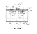
- FIG. 1 a cross section illustrating embodiments of a vertical power MOSFET according to some embodiments of the present invention will be discussed. It will be understood by those having skill in the art that the vertical silicon carbide MOSFETs are generally replicated in a unit cell. Such unit cells are illustrated between lines 100a and 100c or lines 100b and 100c. For ease of illustration, a two unit cell MOSFET will be described, however, as will be appreciated by those of skill in the art, additional unit cells may be incorporated into a MOSFET along one direction or along two, generally orthogonal directions, without departing from the scope of the present invention.
- a MOSFET includes an n + monocrystalline silicon carbide substrate 10, for example, 4H silicon carbide.
- An n - silicon carbide layer 12 is provided on a first face 10A of the substrate 10.
- p + " or "n + " refer to regions that are defined by higher carrier concentrations than are present in adjacent or other regions of the same or another layer or substrate.
- p - " or "n - " refer to regions that are defined by lower carrier concentrations than are present in adjacent or other regions of the same or another layer or substrate.
- an n - substrate could serve as an n - drift layer of the device.
- an n + drain region may be provided on a second face 10B of the n - substrate.
- the n + drain region may be provided by ion implantation or epitaxial growth without departing from the scope of the present invention.
- a p-type silicon carbide region 14 is provided on the n - silicon carbide layer 12 and may provide a p-well region of the MOSFET. It will be understood that the p-well region may be an epitaxial region or an implanted region without departing from the scope of the present invention.
- a buried region 18 of p + silicon carbide is provided in the p-well region 14 beneath an n + region 20 of silicon carbide that is also provided in the p-type region 14.
- the n + region 20 may provide a source region of the device.
- Adjacent and spaced apart from the n + source region 20 is an n-type silicon carbide region 21 that extends through the p-well region 14 to the n - silicon carbide layer 12. It will be understood that in embodiments of the present invention where the p-well region 14 is an epitaxial layer, the n-type silicon carbide region 21 may be termed a Junction Field Effect Transistor (JFET) region of the device.
- JFET Junction Field Effect Transistor
- the n-type silicon carbide region 21 may provide a portion of an n-type channel region 29.
- a surface of the n-type silicon carbide region 21 may include unwanted steps of up to several hundred angstroms each, which may cause increased on resistances and reduced reliability of the device.
- a surface of the p-type region 31 between the n-type silicon carbide region 21 and the buried region 18 of p + silicon carbide may also included these unwanted steps.
- an n - region 19' may be provided on the n-type silicon carbide region 21 and the p-type region 31, which may form a channel region 29 of the device.
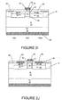
- an n-type epitaxial layer may be regrown on the n-type silicon carbide region 21, the p-type region 31 and other surfaces of the structure and selectively removed such that a portion of the n - region 19' remains on the n-type silicon carbide region 21 and the p-type region 31 of the device, but is removed from the n + source regions 20 as will be discussed further below with respect to Figures 2A through 2J .
- the presence of the n - region 19' on the n-type silicon carbide region 21 and the p-type region 31 may provide a reduction in a surface roughness of the channel region 29 (a combination of the n-type silicon carbide region 21, the p-type region 31 and the remaining portion of the n- region 19').
- the n - region 19' may fill in some of the peaks and valleys on the surface of the n-type silicon carbide region 21 and the p-type region 31 to provide a smoother interface 35 between the channel region 29 and the gate insulating layer 30 (discussed below).
- the channel region 29 may have a root mean square (RMS) surface roughness of less than about 1.0 ⁇ .
- a reduction in the RMS surface roughness of from at least about 28 ⁇ to less than about 1.0 ⁇ may be obtained, which will be discussed further below with respect to Figures 2A through 3C .
- an optional sacrificial oxide layer (not shown) may be provided on a surface of the channel region 29 and subsequently removed.
- the sacrificial oxide layer may have a thickness of from about 100 to about 1000 ⁇ , for example 500 ⁇ .
- the formation and removal of the sacrificial oxide layer may further reduce the RMS surface roughness of the surface of the channel region 29 to about 0.70 ⁇ .
- a gate contact 26 is provided on the gate layer opposite the channel region 29, including the n-type silicon carbide region 21, the p-type region 31 and the n- region 19' .
- Source contact 24 is provided between the n + source regions 20 and a drain contact 28 is provided on a second face 10B of the substrate 10 opposite the p-type region 14.
- the MOSFET may include a hybrid well structure as described in commonly assigned United States Patent Application Serial No. 10/873,394, filed June 22, 2004 , entitled Silicon Carbide Devices With Hybrid Well Regions And Methods Of Fabricating Silicon Carbide Devices With Hybrid Well Regions, the disclosure of which is incorporated herein by reference as if set forth fully herein.
- an n - epitaxial layer 12 is formed on a n + silicon carbide substrate 10, for example, a 4H silicon carbide substrate.
- the n - layer 12 may have a thickness of from about 5 to about 200 ⁇ m and a doping to provide a carrier concentration of from about 1x10 14 cm -3 to about 1x10 17 cm -1 .
- the n-layer 12 is about 12 ⁇ m thick and is doped to provide a carrier concentration of about 5x10 15 cm -3 .
- a p-type layer 14 is provided on the n - epitaxial layer 12.
- the p-type layer 14 may provide a p-well region of the device.
- the p-type layer 14 may be an epitxial region or an implanted region without departing from the scope of the present invention.
- p-type silicon carbide dopants may be implanted in the n - layer 12 to provide the p-type layer 14.
- the p-type layer 14 may be grown on the n - layer 12.
- the p-type layer 14 may have a thickness of from about 0.5 to about 3 ⁇ m and a doping to provide a carrier concentration of from about 2x10 16 cm -3 to about 5x10 17 cm -3 .
- the p-type layer 14 is about 0.5 ⁇ m thick and is doped to provide a carrier concentration of about 1x10 16 cm -3 .
- a mask layer 100 is formed on the p-type layer 14 and patterned to form openings corresponding to the source regions 20 and the buried p-type regions 18 of the device.
- the buried p-type regions 18 and the source regions 20 may be formed by patterning a mask layer 100 having openings corresponding to the location of the source regions 20.
- the buried p-type regions 18 are formed by ion implantation of p-type dopants using the patterned mask 100.
- the buried p-type regions 18 may extend to and, in some embodiments, into the drift region, for example, n - layer 12.
- the p-type dopant may be, for example, aluminum or other suitable p-type dopant.
- the p-type region 18 has a thickness of less than about the thickness to which the region 21 may be formed, for example, from about 0.2 ⁇ m to about 1 ⁇ m.
- the buried p-type regions 18 extend from a depth of about 0.2 ⁇ m to a depth of about 0.7 ⁇ m from the surface of the p-type layer 14.
- the p-type region 18 may be doped to provide a carrier concentration of from about 1 x 10 17 cm -3 to about 1 x 10 18 cm -3 .
- the source regions 20 are formed by implanting n-type dopants into the p-type layer 14 utilizing the patterned mask 100.
- the n-type dopant used for n-type implants may be, for example, nitrogen and/or phosphorus, however, other n-type dopants may also be used.
- the n-type source regions 20 may extend a distance of from about 0.2 ⁇ m to about 0.3 ⁇ m into the p-type layer.
- the n-type source regions 20 may be doped to provide a carrier concentration sufficient to allow for formation of a good ohmic contact.
- the n-type source regions extend to a depth of about 0.2 ⁇ m into the p-type layer and are doped to provide a carrier concentration of at least from about 1x10 19 cm -3 to about 1x10 20 cm -3 .
- the mask 100 may be removed and an n-type silicon carbide region 21 of the device may be provided in the p-well region 14.
- the n-type silicon carbide region 21 may be an implanted region or an epitaxial region without departing from the scope of the present invention.
- a second mask layer 120 may be patterned to have opening corresponding to the n-type silicon carbide region 21 of the device as illustrated in Figure 2D .
- the n-type silicon carbide region 21 may be termed a Junction Field Effect Transistor (JFET) region of the device.
- JFET Junction Field Effect Transistor
- the n-type silicon carbide region 21 may be formed by implanting n-type dopants in the p-type layer 14 utilizing the patterned mask 120 so as to form the n-type silicon carbide region 21 that extends through the p-type layer 14 to the drift region, for example, the n-type epitaxial layer 12. Any suitable n-type dopants may be used. In some embodiments of the present invention, nitrogen is used as the n-type dopant
- the n-type region 21 can provide a path from the MOS channel to the lightly doped drift region ( 12 ), allowing electrons to flow from source regions to drain regions.
- this n-channel region may be depleted of electrons from the reverse biased pn junction, which is formed on both sides of the channel region.
- the pn-junctions on both sides of the channel region may shield the MOS region from high electric fields at off state, which may result in a higher device reliability compared to trench devices, such as MOSFETS.
- Figure 2F illustrates the formation of an optional cap layer 140 of a deposited oxide and/or other passivating material.
- the cap layer 140 may have a thickness of from about 0.01 ⁇ m to about 1 ⁇ m.
- the device may be exposed to a high temperature anneal ranging from about 900°C to about 1800 °C and in some embodiments, about 1600 °C for several minutes, such as five minutes, so as to activate the n-type and p-type implants.
- the cap layer 140 may be removed and an n - silicon carbide epitaxial region 19 may be formed on the channel region 29 of the device.
- a depth of the n - silicon carbide epitaxial region 19 may be controlled so that only a portion of the n - region 19 may be removed from the channel region 29 in a subsequent processing step.
- the n - silicon carbide region may have a thickness of from about 1500 ⁇ to about 6000 ⁇ and a carrier concentration of about 5 x 10 15 cm -3 .
- n - region 19 As illustrated in Figure 2H , a portion of the n - region 19 is removed.
- the portion of the n - region 19' that remains on the n-type silicon carbide region 21 and the p-type region 31 may define the channel region 29 ( Figure 2I) of the device.
- the remaining portion of the n - region 19' may have a thickness of from about 1000 to about 5000 ⁇ . In some embodiments of the present invention, the remaining portion of the n - region 19' may have a thickness of from about 1500 ⁇ .
- the presence of the remaining portion of the n - region 19' on the channel region 29 may provide a reduction in a surface roughness of the channel region 29 at an interface 35 between the n-region 19' and the gate insulator 30, which will be discussed further below with respect to Figure 3 .
- the channel region 29 may be defined by the remaining portion of the n - region 19' and the portion of the p-well 31 between the n-type silicon carbide region 21 and the buried p-type regions 18 and the source regions 20. Accordingly, the n - region 19' may only remain on the portions of the p-well 31 between the n-type silicon carbide region 21 and the buried p-type regions 18 and the source regions 20 and not on the n-type silicon carbide region 21 without departing from the scope of the present invention.
- a chemical mechanical polishing (CMP) process may be performed that removes a portion of the n - region 19 from a surface of the channel region 29.
- the CMP process may remove a portion of the n - region 19 that is from about 2.0 to 3.0 times a depth of the surface roughness of the channel region 29.
- any conventional CMP process may be used as the CMP process discussed herein without departing from the scope of the present invention.
- the process discussed herein does not remove the entire n - region 19.
- implanted regions have a thickness of a few thousand angstroms and conventional CMP processes remove several microns of film during the CMP process to obtain the desired result.
- removal of several microns of film from the structure of Figure 2G would remove all of the implanted region rendering the device non-functional.
- some embodiments of the present invention use a CMP process that removes a portion of the n - region 19, leaving a portion of the n - region 19' remaining on the channel region 29.
- the CMP process may be performed for less than about 3 hours, for example, from about half an hour to about an hour.
- the remaining portion of the n - region may be from about 1000 to about 5000 ⁇ .
- the remaining portion of the n - region 19' on the n-type silicon carbide region 21 and the p-well region 31 become part of the channel region 29, i.
- the remaining portion of the n - region 19' may fill in the peaks and valleys on a surface of the n-type silicon carbide region 21 and the p-well region 31.
- a mask 130 may be provided on the remaining portion of the n - region 19' and the n - region 19' may be patterned according to the mask 130, removing portions of the n - region 19' on the source regions 20 as illustrated in Figure 2I.
- the n- region 19' may only remain on the p-well region 31 between the n-type silicon carbide region 21 and the source regions 20 and the buried p-type regions 18.
- providing the n - region 19' on the n-type region 21 and the p-well region 31 may provide a reduction in the surface roughness between the n - region 19' and the gate insulator 30.
- the surface of the n-type silicon carbide region 21 and the p-well region 31 may have many peaks and valleys after the anneal that activates the implanted regions. These peaks and valleys (several 100 angstroms) may cause suboptimal performance of the device.
- the root mean square (RMS) surface roughness of the channel region 29 may be reduced from at least about 28 ⁇ in Figure 3A to less than about 1.0 ⁇ in Figure 3B according to some embodiments of the present invention.
- an optional sacrificial oxide layer may be formed on a surface of the channel region 29 and removed.
- the formation and removal of the sacrificial oxide layer may further reduce the RMS surface roughness to about 0.70 ⁇ as illustrated in Figure 3C .
- a layer 30 of insulating material may be deposited on the device so as to provide a gate insulating material.
- the insulating material may be formed as described in United States Patent No. 6,610,366 , entitled Method of N 2 O annealing an oxide layer on a silicon carbide layer, United States Patent No. 6,767,843 , entitled Method of N 2 O growth of an oxide layer on a silicon carbide layer and/or United States Patent Application Publication No. US2002/0102358A1 , entitled Method of fabricating an oxide layer on a silicon carbide layer utilizing an anneal in a hydrogen environment, the disclosures of which are incorporated herein as if set forth in their entirety.
- the insulating material may be formed as described in Improved Inversion Channel Mobility for 4H-SiC MOSFETs Following High Temperature Anneals in Nitric Oxide to Chung et al., the disclosure of which is incorporated herein by reference as if set forth in its entirety.
- a gate contact 26 may be formed by forming a metal contact on the gate insulating material 30. Suitable gate contact materials include, but are not limited to, aluminum, polysilicon and molybdenum. Furthermore, as will be appreciated by those of skill in the art, a multi-layered gate contact may also be used.
- contact holes may be formed in the insulating material 30' and ohmic contacts may be formed in the contact holes to provide source contacts 24.
- an ohmic contact 28 may be formed on the substrate 10.
- Suitable ohmic contact materials include, but are not limited to, nickel, titanium alloy, and aluminum.
- the deposited metal contacts may then be annealed at a high temperature ranging from about 500 °C to about 1200 °C.
- An overlayer metal may also be deposited on the contacts, for example, to facilitate connection to the device.
- the n-type silicon carbide region 21 may be formed before forming the n + regions 20 without departing from the scope of the present invention.
- the buried p + regions 18 may be formed either before or after formation of the n + regions 20 or the n-type silicon carbide region 21.
- the contacts 24 may be formed by, for example, depositing and patterning a metal layer, and then the insulating layer 30' provided and openings in the insulating layer formed to the contacts 24. Accordingly, the present invention should not be construed as limited to the exact sequence of operations described herein but is intended to encompass other sequences of fabrication that will become apparent to those of skill in the art in light of the present disclosure.
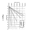
- FIG. 4 a chart illustrating a comparison of Drain Voltage (V) vs. Drain Current (A) for conventional devices and devices fabricated using methods according to some embodiments of the present invention will be discussed. As illustrated in Figure 4 , the drain currents of MOSFETs fabricated according to some embodiments of the present invention are higher than conventional MOSFETS at relative drain voltages.
Abstract
Description
- This invention relates to methods of fabricating power devices and the resulting devices and, more particularly, to silicon carbide power devices and methods of fabricating silicon carbide power devices.
- Power devices are widely used to carry large currents and support high voltages. Modem power devices are generally fabricated from monocrystalline silicon semiconductor material. One widely used power device is the power Metal Oxide Semiconductor Field Effect Transistor (MOSFET). In a power MOSFET, a control signal is supplied to a gate electrode that is separated from the semiconductor surface by an intervening insulator, which may be, but is not limited to, silicon dioxide. Current conduction occurs via transport of majority carriers, without the presence of minority carrier injection that is used in bipolar transistor operation. Power MOSFETs can provide an excellent safe operating area, and can be paralleled in a unit cell structure.
- As is well known to those having skill in the art, power MOSFETs may include a lateral structure or a vertical structure. In a lateral structure, the drain, gate and source terminals are on the same surface of a substrate. In contrast, in a vertical structure, the source and drain are on opposite surfaces of the substrate.
- One widely used silicon power MOSFET is the double diffused MOSFET (DMOSFET), which is fabricated using a double-diffusion process. In these devices, a p-base region and an n+ source region are diffused through a common opening in a mask. The p-base region is driven in deeper than the n+ source. The difference in the lateral diffusion between the p-base and n+ source regions forms a surface channel region. An overview of power MOSFETs including DMOSFETs may be found in the textbook entitled " Power Semiconductor Devices" by B.J. Baliga, published by PWS Publishing Company, 1996, and specifically in Chapter 7, entitled "Power MOSFET", the disclosure of which is hereby incorporated herein by reference.
- Development efforts in power devices have also included investigation of the use of silicon carbide (SiC) devices for power devices. Silicon carbide has a wide bandgap, a lower dielectric constant, a high breakdown field strength, a high thermal conductivity, and a high saturation electron drift velocity compared to silicon. These characteristics may allow silicon carbide power devices to operate at higher temperatures, higher power levels and with lower specific on-resistance than conventional silicon-based power devices. A theoretical analysis of the superiority of silicon carbide devices over silicon devices is found in a publication by Bhatnagar et al. entitled "Comparison of 6H-SiC, 3C-SiC and Si for Power Devices", IEEE Transactions on Electron Devices, Vol. 40, 1993, pp. 645-655. A power MOSFET fabricated in silicon carbide is described in
U.S. Patent No. 5,506,421 to Palmour entitled "Power MOSFET in Silicon Carbide" and assigned to the assignee of the present invention. Silicon Carbide power devices are also described inU.S. Patent No. 6,107,142 to Suvorov et al. , entitled Self-Aligned Methods of Fabricating Silicon Carbide Power Devices by Implantation and Lateral Diffusion andU.S. Patent No. 6,100,169 to Suvorov et. al., entitled Methods of Fabricating Silicon Carbide Power Devices by Controlled Annealing, both of which are assigned to the assignee of the present invention. - Notwithstanding these potential advantages, it may be difficult to fabricate power devices including power MOSFETs in silicon carbide. For example, as described above, the double-diffused MOSFET (DMOSFET) is generally fabricated in silicon using a double diffusion process wherein the p-base region is driven in deeper than the n+ source. Unfortunately, in silicon carbide, the diffusion coefficients of conventional p and n-type dopants are small compared to silicon, so that it may be difficult to obtain the required depths of the p-base and n+ source regions using acceptable diffusion times and temperatures. Ion implantation may also be used to implant the p-base and the n+ source. See, for example, " High-Voltage Double-Implanted Power MOSFET's in 6H-SiC" by Shenoy et al., IEEE Electron Device Letters, Vol. 18, No. 3, March 1997, pp. 93-95. However, it may be difficult to control the depth and lateral extent of ion implanted regions. Moreover, the need to form a surface channel surrounding the source region may require the use of two separate implantation masks. It may then be difficult to align the p-base and the source regions to one another, thereby potentially impacting the device performance. Furthermore, performing a series implants and implant activation anneals may result in step bunched surfaces across the channel of the MOSFET, which may diminish device performance in terms of, for example, increased on resistance and reduced reliability.
- Some embodiments of the present invention provide methods of forming silicon carbide power devices. An n- silicon carbide layer is provided on a silicon carbide substrate. A p-type silicon carbide well region is provided on the n-silicon carbide layer. A buried region of p+ silicon carbide is provided on the p-type silicon carbide well region. An n+ region of silicon carbide is provided on the buried region of p+ silicon carbide. A channel region of the power device is adjacent the buried region of p+ silicon carbide and the n+ region of silicon carbide. An n- region is provided on the channel region and a portion of the n- region is removed from the channel region so that a portion of the n- region remains on the channel region to provide a reduction in a surface roughness of the channel region.
- In further embodiments of the present invention, a portion of the n-region may be removed using a chemical mechanical polishing (CMP) process that removes a portion of the n-region from the channel region. The CMP process may remove all but from about 1000 to about 5000 Å of the n- region. A portion of the n-region that is from about 2.0 to about 3.0 times a depth of the surface roughness of the channel region may be removed. In certain embodiments of the present invention about 1500 Å of the n- region remains on the channel region after the CMP process.
- In still further embodiments of the present invention, the reduction in the surface roughness may be a reduction in a root mean square (RMS) surface roughness of from at least about 28 Å to less than about 1.0 Å. A sacrificial oxide layer having a thickness of from about 100 to about 1000 Å may be formed on the remaining portion of the n- region on the channel region and removed. The RMS surface roughness may be further reduced by the formation and removal of the sacrificial oxide layer from less than about 1.0 Å to about 0.70 Å.
- In some embodiments of the present invention, the n- region may be an n- epitaxial layer that is grown on the channel region to a predetermined thickness such that a portion of the n- epitaxial layer remains on the channel region after removal of a portion of the n- epitaxial layer. In certain embodiments of the present invention, the predetermined thickness of the n- epitaxial layer may be from about 1500 Å to about 5000 Å. The CMP process may be followed by selectively etching the n- region such that the n- region is removed from the n+ region.
- In further embodiments of the present invention, the p-type silicon carbide well region may be formed by implanting p-type dopants in the n- silicon carbide layer. The buried region of p+ silicon carbide may be formed by implanting p-type dopants in the p-type silicon carbide well region. The n+ region of silicon carbide may be formed by implanting n-type dopants in the p-type silicon carbide well region on the buried region of p+ silicon carbide. The implanted dopants may be activated by exposing the implanted dopants to a temperature of greater than about 1600 °C.
- In still further embodiments of the present invention, the p-type silicon carbide well region may be a p-type epitaxial layer on the n- silicon carbide layer. The buried regions of p+ silicon carbide may be formed by implanting p-type silicon carbide dopants on the p-type silicon carbide well region. The n+ regions of silicon carbide may be formed by implanting n-type silicon carbide dopants in the p-type silicon carbide well region on the buried region of p+ silicon carbide.
- In some embodiments of the present invention, an n-type region of silicon carbide may be formed in the p-type silicon carbide well region adjacent the channel region. The channel region may be defined between the buried region of p+ silicon carbide and the n-type region of silicon carbide. The n-type region of silicon carbide may be a Junction Field Effect Transistor (JFET) region of the silicon carbide power device.
- In further embodiments of the present invention, an n-type region of silicon carbide may be formed in the p-type silicon carbide well region adjacent the channel region. The channel region may be defined between the buried region of p+ silicon carbide and the n-type region of silicon carbide. The n- region may only remain on the channel region.
- In still further embodiments of the present invention, the substrate may be an n- substrate, which serves as a drift region of the silicon carbide power device. An n+ drain region may be provided on the substrate opposite the n- silicon carbide layer. The n+ drain region may be an implanted region or an epitaxial region. In certain embodiments of the present invention, the silicon carbide power device may be a Metal Oxide Semiconductor Field Effect Transistor (MOSFET).
- Some embodiments of the present invention provide methods of forming silicon carbide power devices. A silicon carbide epitaxial region is grown on a channel region of the power device. A portion of the silicon carbide epitaxial region is mechanically removed such that a remaining portion of the silicon carbide epitaxial region provides a reduction in a surface roughness of the channel region.
- In still further embodiments of the present invention, the reduction in the surface roughness may be a reduction in the RMS surface roughness of from at least about 28 Å to less than about 1.0 Å. In certain embodiments of the present invention, a sacrificial oxide layer may be formed on the silicon carbide epitaxial region and the sacrificial oxide layer may be removed to provide a further reduction in the surface roughness of the channel region. The RMS surface roughness may be further reduced by the formation and removal of the sacrificial oxide layer from less than about 1.0 Å to about 0.70 Å.
-
- 1. A method of forming a silicon carbide power device, comprising: forming an n-silicon carbide layer on a silicon carbide substrate; forming a p-type silicon carbide well region on the n- silicon carbide layer; forming a buried region of p+ silicon carbide in the p-type silicon carbide well region; forming an n+ region of silicon carbide on the buried region of p+ silicon carbide, a channel region of the power device being adjacent the buried region of p+ and n region of silicon carbide; forming an n- region on the channel region; and removing a portion of the n- region from the channel region so that a portion of the n- region remains on the channel region to provide a reduction in a surface roughness of the channel region.
- 2. The method of
Clause 1, wherein removing comprises performing a chemical mechanical polishing (CMP) process that removes a portion of the n- region from the channel region. - 3. The method of Clause 2, wherein the CMP process removes all but from about 1000 to about 5000 Å of the n- region from the channel region.
- 4. The method of Clause 2, wherein removing further comprises removing a portion of the n- region that is from about 2.0 to about 3.0 times a depth of the surface roughness of the channel region.
- 5. The method of Clause 4, wherein about 1500 Å of the n- region remains on the channel region after the CMP process.
- 6. The method of
Clause 1, wherein the reduction in the surface roughness is a reduction in a root mean square (RMS) surface roughness of from at least about 28 Å to less than about 1.0 Å. - 7. The method of Clause 6, wherein removing is followed by: forming a sacrificial oxide layer on the remaining portion of the n- region on the channel region, the sacrificial layer having a thickness of from about 100 to about 1000 Å; and removing the sacrificial oxide layer, wherein the RMS surface roughness is further reduced by the formation and removal of the sacrificial oxide layer from less than about 1.0 Å to about 0.70 Å.
- 8. The method of
Clause 1, wherein forming the n- region comprises growing an n- epitaxial layer on the channel region to a predetermined thickness such that a portion of the n- epitaxial layer remains on the channel region after removal of the portion of the n- epitaxial layer. - 9. The method of Clause 8, wherein the predetermined thickness of the n-epitaxial layer is from about 1500 Å to about 6000 Å.
- 10. The method of Clause 2, wherein performing the CMP process is followed by selectively etching the n- region such that the n+ region is removed from the n region.
- 11. The method of
Clause 1, wherein forming the p-type silicon carbide well region comprises implanting p-type dopants in the n silicon carbide layer; wherein forming the buried region of p+ silicon carbide comprises implanting p-type dopants in the p-type silicon carbide well region; and wherein forming the n+ region of silicon carbide comprises implanting n-type dopants in the p-type silicon carbide well region on the buried region of p+ silicon carbide. - 12. The method of Clause 11, further comprising activating the implanted dopants by exposing the implanted dopants to a temperature of greater than about 1600°C.
- 13. The method of Clause 2 wherein forming the p-type silicon carbide well region comprises forming a p-type epitaxial layer on the n- silicon carbide layer; wherein forming the buried region of p+ silicon carbide comprises implanting p-type silicon carbide dopants in the p-type silicon carbide well region; and wherein forming the n+ region of silicon carbide comprises implanting n-type silicon carbide dopants in the p-type silicon carbide well region on the first and second p+ regions of silicon carbide.
- 14. The method of Clause 13, further comprising forming an n-type region of silicon carbide in the p-type silicon carbide well region adjacent the channel region, wherein the channel region is defmed between the buried region of p+ silicon carbide and the n-type region of silicon carbide and wherein the n-type region of silicon carbide is a Junction Field Effect Transistor (JFET) region of the silicon carbide power device.
- 15. The method of
Clause 1, further comprising forming an n-type region of silicon carbide in the p-type silicon carbide well region adjacent the channel region, wherein the channel region is defined between the buried region of p+ silicon carbide and the n-type region of silicon carbide and wherein the n- region only remains on the channel region. - 16. The method of
Clause 1, wherein the substrate comprises an n- substrate which serves as a drift region of the silicon carbide power device, the method further comprising forming an n+ drain region on the substrate opposite the n- silicon carbide layer. - 17. The method of Clause 16, wherein forming the n+ drain region comprises at least one of implanting the n+ drain region in the n- substrate or growing the n+ drain region on the n- substrate.
- 18. The method of
Clause 1, wherein the silicon carbide power device comprises a Metal Oxide Semiconductor Field Effect Transistor (MOSFET). - 19. A method of forming a silicon carbide power device, comprising: growing a silicon carbide epitaxial region on a channel region of the power device; and mechanically removing a portion of the silicon carbide epitaxial region such that a remaining portion of the silicon carbide epitaxial region on the channel region provides a reduction in a surface roughness of the channel region.
- 20. The method of
Clause 19, wherein the reduction in the surface roughness is a reduction in a root mean square (RMS) surface roughness of from at least about 28 Å to less than about 1.0 Å. - 21. The method of
Clause 20, further comprising: forming a sacrificial oxide layer on the remaining portion of the silicon carbide epitaxial region, the sacrificial oxide layer having a thickness of from about 100 to about 1000 Å; and removing the sacrificial oxide layer to provide a further reduction in the surface roughness of the channel region. - 22. The method of
Clause 21 , wherein the RMS surface roughness is further reduced by the formation and removal of the sacrificial oxide layer from less than about 1.0 Å to about 0.70 Å. - 23. The method of
Clause 19, wherein mechanically removing comprises performing a chemical mechanical polishing (CMP) process that removes a portion of the silicon carbide epitaxial region from the channel region. - 24. The method of Clause 23 , wherein a remaining portion of the silicon carbide epitaxial region after the CMP process has a thickness of from about 1000 to about 5000 Å.
- 25. The method of
Clause 19, wherein mechanically removing further comprises mechanically removing a portion of the silicon carbide epitaxial region that is from about 2 to about 3 times a depth of the surface roughness of the channel region. - 26. The method of Clause 25, wherein a remaining portion of the silicon carbide epitaxial region has a thickness of from about 1500 Å.
- 27. The method of
Clause 19, wherein the silicon carbide epitaxial region has a thickness from about 1500 Å to about 6000 Å. - 28. The method of
Clause 19, wherein mechanically removing is followed by selectively etching the silicon carbide epitaxial region to expose an underlying region while a portion of the silicon carbide epitaxial region remains on the channel region of the power device. - 29. The method of
Clause 19, further comprising: forming an n- silicon carbide layer on a silicon carbide substrate; forming a p-type silicon carbide well region on the n-silicon carbide layer; forming first and second spaced apart buried regions of p+ silicon carbide in the p-type silicon carbide well region; and forming first and second spaced apart n+ regions of silicon carbide on the first and second p+ regions of silicon carbide, respectively, such that the channel region of the power device is defined between the first p+ and n+ regions of silicon carbide and the second p+ and n+ regions of silicon carbide. - 30. The method of
Clause 29, wherein forming the p-type silicon carbide well region comprises implanting p-type dopants in the n- silicon carbide layer; wherein forming the first and second spaced apart buried regions of p+ silicon carbide comprises implanting p-type dopants in the p-type silicon carbide well region; and wherein forming the first and second spaced apart n+ regions of silicon carbide comprises implanting n-type dopants in the p-type silicon carbide well region on the first and second p+ regions of silicon carbide. - 31. The method of
Clause 30, further comprising activating the implanted dopants by exposing the implanted dopants to a temperature of greater than about 1600°C. -
-
Figure 1 is a cross section illustrating power MOSFETs according to some embodiments of the present invention. -
Figures 2A through 2J are cross sections illustrating processing steps in the fabrication of the power MOSFETs ofFigure 1 according to some embodiments of the present invention. -
Figures 3A through 3C are images of channels of MOSFETS fabricated using methods according to some embodiments of the present invention. -
Figure 4 is a chart illustrating a comparison of Drain Voltage (V) vs. Drain Current (A) for conventional devices and devices fabricated using methods according to some embodiments of the present invention. - The present invention now will be described more fully hereinafter with reference to the accompanying drawings, in which embodiments of the invention are shown. This invention may, however, be embodied in many different forms and should not be construed as limited to the embodiments set forth herein. Rather, these embodiments are provided so that this disclosure will be thorough and complete, and will fully convey the scope of the invention to those skilled in the art. In the drawings, the size and relative sizes of layers and regions may be exaggerated for clarity. It will be understood that when an element or layer is referred to as being "on", "connected to" or "coupled to" another element or layer, it can be directly on, connected or coupled to the other element or layer or intervening elements or layers may be present. In contrast, when an element is referred to as being "directly on," "directly connected to" or "directly coupled to" another element or layer, there are no intervening elements or layers present. Like numbers refer to like elements throughout. As used herein, the term "and/or" includes any and all combinations of one or more of the associated listed items.
- It will be understood that, although the terms first, second, etc. may be used herein to describe various elements, components, regions, layers and/or sections, these elements, components, regions, layers and/or sections should not be limited by these terms. These terms are only used to distinguish one element, component, region, layer or section from another element, component, region, layer or section. Thus, a first element, component, region, layer or section discussed below could be termed a second element, component, region, layer or section without departing from the teachings of the present invention.
- Furthermore, relative terms, such as "lower" or "bottom" and "upper" or "top," may be used herein to describe one element's relationship to another elements as illustrated in the Figures. It will be understood that relative terms are intended to encompass different orientations of the device in addition to the orientation depicted in the Figures. For example, if the device in the Figures is turned over, elements described as being on the "lower" side of other elements would then be oriented on "upper" sides of the other elements. The exemplary term "lower", can therefore, encompass both an orientation of "lower" and "upper," depending on the particular orientation of the figure. Similarly, if the device in one of the figures is turned over, elements described as "below" or "beneath" other elements would then be oriented "above" the other elements. The exemplary terms "below" or "beneath" can, therefore, encompass both an orientation of above and below.
- Embodiments of the present invention are described herein with reference to cross-section illustrations that are schematic illustrations of idealized embodiments of the present invention. As such, variations from the shapes of the illustrations as a result, for example, of manufacturing techniques and/or tolerances, are to be expected. Thus, embodiments of the present invention should not be construed as limited to the particular shapes of regions illustrated herein but are to include deviations in shapes that result, for example, from manufacturing. For example, an implanted region illustrated as a rectangle will, typically, have rounded or curved features and/or a gradient of implant concentration at its edges rather than a binary change from implanted to non implanted region. Likewise, a buried region formed by implantation may result in some implantation in the region between the buried region and the surface through which the implantation takes place. Thus, the regions illustrated in the figures are schematic in nature and their shapes are not intended to illustrate the precise shape of a region of a device and are not intended to limit the scope of the present invention.
- Embodiments of the present invention are described with reference to a particular polarity conductivity type for various layers/regions. However, as will be appreciated by those of skill in the art, the polarity of the regions/layers may be inverted to provide an opposite polarity device.
- Some embodiments of the present invention prevention provide power Metal Oxide Semiconductor Field Effect Transistors (MOSFETs) and/or other power devices that may include doped regions of silicon carbide. As is known to those of skill in the art, doped regions of silicon carbide may be formed through epitaxial growth and/or through implantation. For example, a p-type region of silicon carbide may be formed through epitaxial growth in the presence of a p-type dopant or through implantation of p-type dopants in an undoped, p-type or n-type epitaxial layer. The structure that results from epitaxial growth differs from that that results from implantation. Thus, the terms "epitaxial region" and "implanted region" structurally distinguish differing regions of silicon carbide and may be used herein as a recitation of structural characteristics of the regions of silicon carbide and/or as recitations of methods of forming such regions of silicon carbide.
- While embodiments of the present invention are described with reference to MOSFETs, embodiments of the present invention may be used in other devices, such as laterally-diffused MOSFETs (LDMOSFETs), Insulated Gate Bipolar Transistors (IGBTs) or other such MOS based devices as well as high voltage devices, such as Schottky and PiN diodes without departing from the scope of the present invention.
- Surface morphology is a concern in the development of commercial silicon carbide (SiC) power devices, such as SiC power MOSFETs. The series of implantation steps and implant activation anneals may result in step-bunched surfaces across a channel of the device. The steps created on the surface of the device may be several hundred angstroms, which may cause increased on resistances and reduced reliability of the device. Methods according to some embodiments of the present invention may provide channel regions having reduced surface roughness so as to improve overall device performance. In particular, methods of fabricating power devices according to some embodiments of the present invention may provide an additional n- region on the channel region. In particular, an n- region may be formed on the channel region of the device, a portion of which is removed, such that a remaining portion of the n- region on the channel region provides a reduced surface roughness of the channel region. Thus, at least a portion of the step-bunched surface may be removed from the channel region to provide a smoother channel region, i.e., a channel region with reduced surface roughness. In some embodiments, the removal process is performed using a chemical mechanical polishing process that may remove a portion of, or from about 1200 Å to about 1400 Å, of the n- region from the channel region. The remaining portion of the n- region may provide a reduction in a root mean square (RMS) surface roughness of the channel region of from about at least 28 Å to less than about 1.0 Å as will be discussed further below with respect to
Figures 1 through 4 . - Referring now to
Figure 1 , a cross section illustrating embodiments of a vertical power MOSFET according to some embodiments of the present invention will be discussed. It will be understood by those having skill in the art that the vertical silicon carbide MOSFETs are generally replicated in a unit cell. Such unit cells are illustrated betweenlines lines - As illustrated in
Figure 1 , a MOSFET according to some embodiments of the present invention includes an n+ monocrystallinesilicon carbide substrate 10, for example, 4H silicon carbide. An n-silicon carbide layer 12 is provided on afirst face 10A of thesubstrate 10. As used herein, "p+ " or "n+ " refer to regions that are defined by higher carrier concentrations than are present in adjacent or other regions of the same or another layer or substrate. Similarly, "p- " or "n-" refer to regions that are defined by lower carrier concentrations than are present in adjacent or other regions of the same or another layer or substrate. - In some embodiments of the present invention, an n- substrate could serve as an n- drift layer of the device. In these embodiments of the present invention, an n+ drain region may be provided on a
second face 10B of the n- substrate. The n+ drain region may be provided by ion implantation or epitaxial growth without departing from the scope of the present invention. - A p-type
silicon carbide region 14 is provided on the n-silicon carbide layer 12 and may provide a p-well region of the MOSFET. It will be understood that the p-well region may be an epitaxial region or an implanted region without departing from the scope of the present invention. - A buried
region 18 of p+ silicon carbide is provided in the p-well region 14 beneath an n+ region 20 of silicon carbide that is also provided in the p-type region 14. The n+ region 20 may provide a source region of the device. Adjacent and spaced apart from the n+ source region 20 is an n-typesilicon carbide region 21 that extends through the p-well region 14 to the n-silicon carbide layer 12. It will be understood that in embodiments of the present invention where the p-well region 14 is an epitaxial layer, the n-typesilicon carbide region 21 may be termed a Junction Field Effect Transistor (JFET) region of the device. - The n-type
silicon carbide region 21 may provide a portion of an n-type channel region 29. A surface of the n-typesilicon carbide region 21 may include unwanted steps of up to several hundred angstroms each, which may cause increased on resistances and reduced reliability of the device. Furthermore, a surface of the p-type region 31 between the n-typesilicon carbide region 21 and the buriedregion 18 of p+ silicon carbide may also included these unwanted steps. Thus, as illustrated inFigure 1 , an n- region 19' according to some embodiments of the present invention may be provided on the n-typesilicon carbide region 21 and the p-type region 31, which may form achannel region 29 of the device. In particular, an n-type epitaxial layer may be regrown on the n-typesilicon carbide region 21, the p-type region 31 and other surfaces of the structure and selectively removed such that a portion of the n- region 19' remains on the n-typesilicon carbide region 21 and the p-type region 31 of the device, but is removed from the n+ source regions 20 as will be discussed further below with respect toFigures 2A through 2J . - Regrowth is discussed in detail in commonly assigned United States Patent Application Publication No.
US 2004/0211980 entitled Silicon Carbide Power Devices With Self-Aligned Source And Well Regions and Methods Of Fabricating Same, filed on April 24, 2003; United States Patent Application Publication No.US 2004/0119076 entitled Vertical JFET Limited Silicon Carbide Power Metal-Oxide Semiconductor Field Effect Transistors and Methods of Fabricating Vertical JFET Limited Silicon Carbide Metal-Oxide Semiconductor Field Effect Transistors, filed on October 30, 2003; and United States Patent Application Publication No.US 2002/0038891 entitled Silicon Carbide Power Metal-Oxide Semiconductor Field Effect Transistors Having a Shorting Channel and Methods of Fabricating Silicon Carbide Metal-Oxide Semiconductor Field Effect Transistors Having a Shorting Channel, filed June 24, 2001, the disclosures of which are hereby incorporated herein by reference as if set forth in their entirety. - The presence of the n- region 19' on the n-type
silicon carbide region 21 and the p-type region 31 may provide a reduction in a surface roughness of the channel region 29 (a combination of the n-typesilicon carbide region 21, the p-type region 31 and the remaining portion of the n- region 19'). In other words, the n-region 19' may fill in some of the peaks and valleys on the surface of the n-typesilicon carbide region 21 and the p-type region 31 to provide asmoother interface 35 between thechannel region 29 and the gate insulating layer 30 (discussed below). According to some embodiments of the present invention, thechannel region 29 may have a root mean square (RMS) surface roughness of less than about 1.0 Å. Thus, according to some embodiments of the present invention, a reduction in the RMS surface roughness of from at least about 28 Å to less than about 1.0 Å may be obtained, which will be discussed further below with respect toFigures 2A through 3C . According to some embodiments of the present invention, an optional sacrificial oxide layer (not shown) may be provided on a surface of thechannel region 29 and subsequently removed. The sacrificial oxide layer may have a thickness of from about 100 to about 1000 Å, for example 500 Å. The formation and removal of the sacrificial oxide layer may further reduce the RMS surface roughness of the surface of thechannel region 29 to about 0.70 Å. - A
gate insulating layer 30 of a suitable dielectric material, such as silicon dioxide (SiO2), extends over thechannel region 29 and to the n+ source regions 20. Agate contact 26 is provided on the gate layer opposite thechannel region 29, including the n-typesilicon carbide region 21, the p-type region 31 and the n- region 19'.Source contact 24 is provided between the n+ source regions 20 and adrain contact 28 is provided on asecond face 10B of thesubstrate 10 opposite the p-type region 14. - It will be understood that although embodiments of the present invention are discussed with respect to the MOSFET structure illustrated in
Figure 1 , embodiments of the present invention are not limited to this configuration. For example, in some embodiments of the present invention, the MOSFET may include a hybrid well structure as described in commonly assigned United States Patent Application Serial No.10/873,394, filed June 22, 2004 - Referring now to
Figures 2A through 2J , processing steps in the fabrication of power devices, for example, MOSFETS, according to some embodiments of the present invention will be discussed. As illustrated inFigure 2A , an n- epitaxial layer 12 is formed on a n+silicon carbide substrate 10, for example, a 4H silicon carbide substrate. The n- layer 12 may have a thickness of from about 5 to about 200 µm and a doping to provide a carrier concentration of from about 1x1014 cm-3 to about 1x1017 cm-1. In particular embodiments of the present invention, the n-layer 12 is about 12 µm thick and is doped to provide a carrier concentration of about 5x1015 cm-3 . - A p-
type layer 14 is provided on the n- epitaxial layer 12. As discussed above, the p-type layer 14 may provide a p-well region of the device. The p-type layer 14 may be an epitxial region or an implanted region without departing from the scope of the present invention. In particular, in embodiments of the present invention where the p-type layer 14 is an implanted region, p-type silicon carbide dopants may be implanted in the n- layer 12 to provide the p-type layer 14. In embodiments of the present invention where the p-type layer 14 is an epitaxial layer, the p-type layer 14 may be grown on the n- layer 12. The p-type layer 14 may have a thickness of from about 0.5 to about 3 µm and a doping to provide a carrier concentration of from about 2x1016 cm-3 to about 5x1017 cm-3. In particular embodiments of the present invention, the p-type layer 14 is about 0.5 µm thick and is doped to provide a carrier concentration of about 1x1016 cm-3. As further illustrated inFigure 2A , amask layer 100 is formed on the p-type layer 14 and patterned to form openings corresponding to thesource regions 20 and the buried p-type regions 18 of the device. - As illustrated in
Figures 2B and2C , the buried p-type regions 18 and thesource regions 20 may be formed by patterning amask layer 100 having openings corresponding to the location of thesource regions 20. The buried p-type regions 18 are formed by ion implantation of p-type dopants using the patternedmask 100. The buried p-type regions 18 may extend to and, in some embodiments, into the drift region, for example, n- layer 12. The p-type dopant may be, for example, aluminum or other suitable p-type dopant. In certain embodiments of the present invention, the p-type region 18 has a thickness of less than about the thickness to which theregion 21 may be formed, for example, from about 0.2 µm to about 1 µm. In particular embodiments of the present invention, the buried p-type regions 18 extend from a depth of about 0.2 µm to a depth of about 0.7 µm from the surface of the p-type layer 14. Furthermore, the p-type region 18 may be doped to provide a carrier concentration of from about 1 x 1017 cm-3 to about 1 x 1018 cm-3. - As illustrated in
Figure 2C , thesource regions 20 are formed by implanting n-type dopants into the p-type layer 14 utilizing the patternedmask 100. The n-type dopant used for n-type implants may be, for example, nitrogen and/or phosphorus, however, other n-type dopants may also be used. The n-type source regions 20 may extend a distance of from about 0.2 µm to about 0.3 µm into the p-type layer. The n-type source regions 20 may be doped to provide a carrier concentration sufficient to allow for formation of a good ohmic contact. As used herein the term "ohmic contact" refers to contacts where an impedance associated therewith is substantially given by the relationship of Impedance = V/I, where V is a voltage across the contact and I is the current, at substantially all expected operating frequencies (i.e., the impedance associated with the ohmic contact is substantially the same at all operating frequencies) and currents. In particular embodiments of the present invention, the n-type source regions extend to a depth of about 0.2 µm into the p-type layer and are doped to provide a carrier concentration of at least from about 1x1019 cm-3 to about 1x1020 cm-3. - While embodiments of the present invention are described herein using the same windows in the patterned
mask 100 for implantation of both the p-type regions 18 and thesource regions 20, in some embodiments of the present invention different size windows may be used to compensate for straggle in the implantation. - As illustrated in
Figures 2D through 2E , themask 100 may be removed and an n-typesilicon carbide region 21 of the device may be provided in the p-well region 14. The n-typesilicon carbide region 21 may be an implanted region or an epitaxial region without departing from the scope of the present invention. In embodiments of the present invention where the n-typesilicon carbide region 21 is an implanted region, asecond mask layer 120 may be patterned to have opening corresponding to the n-typesilicon carbide region 21 of the device as illustrated inFigure 2D . It will be understood that in embodiments of the present invention where the p-well region 14 is an epitaxial layer, the n-typesilicon carbide region 21 may be termed a Junction Field Effect Transistor (JFET) region of the device. - As illustrated in
Figure 2E , the n-typesilicon carbide region 21 may be formed by implanting n-type dopants in the p-type layer 14 utilizing the patternedmask 120 so as to form the n-typesilicon carbide region 21 that extends through the p-type layer 14 to the drift region, for example, the n-type epitaxial layer 12. Any suitable n-type dopants may be used. In some embodiments of the present invention, nitrogen is used as the n-type dopant - When the device is turned-on, the n-
type region 21 can provide a path from the MOS channel to the lightly doped drift region (12), allowing electrons to flow from source regions to drain regions. In the off-state, this n-channel region may be depleted of electrons from the reverse biased pn junction, which is formed on both sides of the channel region. The pn-junctions on both sides of the channel region may shield the MOS region from high electric fields at off state, which may result in a higher device reliability compared to trench devices, such as MOSFETS. -
Figure 2F illustrates the formation of anoptional cap layer 140 of a deposited oxide and/or other passivating material. Thecap layer 140 may have a thickness of from about 0.01 µm to about 1 µm. In any event, whether acap layer 140 is utilized or not, the device may be exposed to a high temperature anneal ranging from about 900°C to about 1800 °C and in some embodiments, about 1600 °C for several minutes, such as five minutes, so as to activate the n-type and p-type implants. - As illustrated in
Figure 2G , thecap layer 140 may be removed and an n- siliconcarbide epitaxial region 19 may be formed on thechannel region 29 of the device. A depth of the n-siliconcarbide epitaxial region 19 may be controlled so that only a portion of the n- region 19 may be removed from thechannel region 29 in a subsequent processing step. In some embodiments of the present invention, the n-silicon carbide region may have a thickness of from about 1500 Å to about 6000 Å and a carrier concentration of about 5 x 1015 cm-3. - As illustrated in
Figure 2H , a portion of the n- region 19 is removed. The portion of the n- region 19' that remains on the n-typesilicon carbide region 21 and the p-type region 31 may define the channel region 29(Figure 2I) of the device. The remaining portion of the n- region 19' may have a thickness of from about 1000 to about 5000 Å. In some embodiments of the present invention, the remaining portion of the n- region 19' may have a thickness of from about 1500 Å. The presence of the remaining portion of the n- region 19' on thechannel region 29 may provide a reduction in a surface roughness of thechannel region 29 at aninterface 35 between the n-region 19' and thegate insulator 30, which will be discussed further below with respect toFigure 3 . - It will be understood that that the
channel region 29 may be defined by the remaining portion of the n- region 19' and the portion of the p-well 31 between the n-typesilicon carbide region 21 and the buried p-type regions 18 and thesource regions 20. Accordingly, the n- region 19' may only remain on the portions of the p-well 31 between the n-typesilicon carbide region 21 and the buried p-type regions 18 and thesource regions 20 and not on the n-typesilicon carbide region 21 without departing from the scope of the present invention. - In some embodiments of the present invention, a chemical mechanical polishing (CMP) process may be performed that removes a portion of the n- region 19 from a surface of the
channel region 29. In certain embodiments of the present invention, the CMP process may remove a portion of the n- region 19 that is from about 2.0 to 3.0 times a depth of the surface roughness of thechannel region 29. It will be understood that any conventional CMP process may be used as the CMP process discussed herein without departing from the scope of the present invention. However, the process discussed herein does not remove the entire n- region 19. Typically, implanted regions have a thickness of a few thousand angstroms and conventional CMP processes remove several microns of film during the CMP process to obtain the desired result. However, as will be understood by those having skill in the art, removal of several microns of film from the structure ofFigure 2G would remove all of the implanted region rendering the device non-functional. - Accordingly, some embodiments of the present invention use a CMP process that removes a portion of the n- region 19, leaving a portion of the n- region 19' remaining on the
channel region 29. For example, in some embodiments of the present invention, the CMP process may be performed for less than about 3 hours, for example, from about half an hour to about an hour. In other words, after the CMP process from about 1000 to about 5000 Å of the n-region 19 may remain on thechannel region 29 of the device. Thus, the remaining portion of the n-region may be from about 1000 to about 5000 Å. The remaining portion of the n- region 19' on the n-typesilicon carbide region 21 and the p-well region 31 become part of thechannel region 29, i. e., the remaining portion of the n-region 19' may fill in the peaks and valleys on a surface of the n-typesilicon carbide region 21 and the p-well region 31. As further illustrated inFigure 2H , amask 130 may be provided on the remaining portion of the n- region 19' and the n-region 19' may be patterned according to themask 130, removing portions of the n- region 19' on thesource regions 20 as illustrated inFigure 2I. As discussed above, in some embodiments of the present invention the n- region 19' may only remain on the p-well region 31 between the n-typesilicon carbide region 21 and thesource regions 20 and the buried p-type regions 18. - As discussed above, providing the n- region 19' on the n-
type region 21 and the p-well region 31 may provide a reduction in the surface roughness between the n- region 19' and thegate insulator 30. For example, as illustrated inFigure 3A , the surface of the n-typesilicon carbide region 21 and the p-well region 31 may have many peaks and valleys after the anneal that activates the implanted regions. These peaks and valleys (several 100 angstroms) may cause suboptimal performance of the device. After the forming of the n- region 19 on the n-typesilicon carbide region 21 and the p-well region 31 and the removal of a portion of the n- region from the n-typesilicon carbide region 21 and the p-well region 31 according to some embodiments of the present invention, many of the peaks and valleys may be removed by the presence of the remaining portion of the n- region 19' as illustrated inFigure 3 B. In particular, the root mean square (RMS) surface roughness of thechannel region 29 may be reduced from at least about 28 Å inFigure 3A to less than about 1.0 Å inFigure 3B according to some embodiments of the present invention. Furthermore, in some embodiments of the present invention, an optional sacrificial oxide layer (not shown) may be formed on a surface of thechannel region 29 and removed. The formation and removal of the sacrificial oxide layer may further reduce the RMS surface roughness to about 0.70 Å as illustrated inFigure 3C . - As illustrated in
Figure 2I, alayer 30 of insulating material may be deposited on the device so as to provide a gate insulating material. In some embodiments of the present invention, the insulating material may be formed as described in United States Patent No.6,610,366 , entitled Method of N2O annealing an oxide layer on a silicon carbide layer, United States Patent No.6,767,843 , entitled Method of N2O growth of an oxide layer on a silicon carbide layer and/or United States Patent Application Publication No.US2002/0102358A1 , entitled Method of fabricating an oxide layer on a silicon carbide layer utilizing an anneal in a hydrogen environment, the disclosures of which are incorporated herein as if set forth in their entirety. In certain embodiments of the present invention, the insulating material may be formed as described in Improved Inversion Channel Mobility for 4H-SiC MOSFETs Following High Temperature Anneals in Nitric Oxide to Chung et al., the disclosure of which is incorporated herein by reference as if set forth in its entirety. As further illustrated inFigure 2I , agate contact 26 may be formed by forming a metal contact on thegate insulating material 30. Suitable gate contact materials include, but are not limited to, aluminum, polysilicon and molybdenum. Furthermore, as will be appreciated by those of skill in the art, a multi-layered gate contact may also be used. - As is illustrated in
Figure 2 J, contact holes may be formed in the insulating material 30' and ohmic contacts may be formed in the contact holes to providesource contacts 24. Similarly, anohmic contact 28 may be formed on thesubstrate 10. Suitable ohmic contact materials include, but are not limited to, nickel, titanium alloy, and aluminum. The deposited metal contacts may then be annealed at a high temperature ranging from about 500 °C to about 1200 °C. An overlayer metal may also be deposited on the contacts, for example, to facilitate connection to the device. - It will be understood by those having skill in the art that the order of steps in
Figures 2A through 2J may be changed. Thus, for example, the n-typesilicon carbide region 21 may be formed before forming the n+ regions 20 without departing from the scope of the present invention. Similarly, the buried p+ regions 18 may be formed either before or after formation of the n+ regions 20 or the n-typesilicon carbide region 21. Similarly, thecontacts 24 may be formed by, for example, depositing and patterning a metal layer, and then the insulating layer 30' provided and openings in the insulating layer formed to thecontacts 24. Accordingly, the present invention should not be construed as limited to the exact sequence of operations described herein but is intended to encompass other sequences of fabrication that will become apparent to those of skill in the art in light of the present disclosure. - Referring now to
Figure 4 , a chart illustrating a comparison of Drain Voltage (V) vs. Drain Current (A) for conventional devices and devices fabricated using methods according to some embodiments of the present invention will be discussed. As illustrated inFigure 4 , the drain currents of MOSFETs fabricated according to some embodiments of the present invention are higher than conventional MOSFETS at relative drain voltages. - In the drawings and specification, there have been disclosed typical preferred embodiments of the invention and, although specific terms are employed, they are used in a generic and descriptive sense only and not for purposes of limitation, the scope of the invention being set forth in the following claims.
Claims (16)
- A power device, comprising:a p-type conductivity well region;a buried p+ conductivity region in the p-type conductivity well region;an n+ conductivity region on the buried p+ conductivity region; anda channel region of the power device adjacent the buried p+ conductivity region and n+ conductivity region, the channel region of the power device having a root mean square (RMS) surface roughness of less than about 1.0 Å.
- The device of Claim 1:
wherein the p-type conductivity well region comprises a p-type silicon carbide well region;
wherein the buried p+ conductivity region comprises a buried region of p+ silicon carbide in the p-type silicon carbide well region; and
wherein the n+ conductivity region comprises an n+ region of silicon carbide on the buried region of p+ silicon carbide. - A Metal Oxide Semiconductor Field Effect Transistor (MOSFET) device comprising a channel region having a root mean square (RMS) surface roughness of less than about 1.0 Å.
- The device of Claim 2 or claim 3, further comprising a sacrificial oxide layer on a surface of the channel region having a thickness of from about 100 to about 1000 Å, herein the RMS surface roughness of the channel region is reduced to about 0.70 Å after formation of the sacrificial oxide layer.
- The device of Claim 2 or claim 3, further comprising an n- silicon carbide region on the channel region of the power device, the presence of the n- silicon carbide region providing a reduction in a surface roughness of the channel region, wherein the reduction in the surface roughness is a reduction in a root mean square (RMS) surface roughness of from at least about 28 Å to less than about 1.0 Å.
- The device of Claim 2 or claim 3, further comprising an n- silicon carbide region on the channel region of the power device, the presence of the n- silicon carbide region providing a reduction in a surface roughness of the channel region, wherein n-region of silicon carbide on the channel region has a thickness of from about 1000 to about 5000 Å and wherein the thickness of the n- region of silicon carbide on the channel region is about 1500 Å
- The device of Claim 5, further comprising an n- silicon carbide region on the channel region of the power device, the presence of the n- silicon carbide region providing a reduction in a surface roughness of the channel region, wherein the n- region comprises a remaining portion of an n- epitaxial layer on the channel region after removal of a removed portion of the n- epitaxial layer and wherein the n- epitaxial layer has a thickness of from about 1500 Å to about 6000 Å before removal of the removed portion thereof.
- The device of Claim 5 when dependent upon claim 2, further comprising an n- silicon carbide region on the channel region of the power device, the presence of the n- silicon carbide region providing a reduction in a surface roughness of the channel region further comprising an n-type region of silicon carbide in the p-type silicon carbide well region adjacent the channel region, wherein the channel region is defined between the buried region of p+ silicon carbide and the n-type region of silicon carbide and wherein the n- region only remains on the channel region.
- The device of Claim 2, further comprising;
a silicon carbide substrate, wherein the p-type silicon carbide well region is provided on the silicon carbide substrate; and
an n- silicon carbide layer between the silicon carbide substrate and the p-type silicon carbide well region,
wherein the p-type silicon carbide well region comprises an implanted region of p-type silicon carbide in the n- silicon carbide layer;
wherein the buried region of p+ silicon carbide comprises an implanted region of p+ silicon carbide in the p-type silicon carbide well region; and
wherein the n+ region of silicon carbide comprises an implanted n-type region in the p-type silicon carbide well region on the buried region of p+ silicon carbide. - The device of Claim 2, further comprising:a silicon carbide substrate, wherein the p-type silicon carbide well region is provided on the silicon carbide substrate; andan n- silicon carbide layer between the silicon carbide substrate and the p-type silicon carbide well region,wherein the p-type silicon carbide well region comprises a p-type epitaxial layer on the n- silicon carbide layer;
wherein the buried region of p+ silicon carbide comprises an implanted region of p-type silicon carbide in the p-type silicon carbide well region; and
wherein the n+ region of silicon carbide comprises an implanted region of n-type silicon carbide in the p-type silicon carbide well region on the p+ region of silicon carbide. - The device of Claim 2, further comprising an n-type region of silicon carbide in the p-type silicon carbide well region adjacent the channel region, wherein the channel region is defined between the buried region of p+ silicon carbide and the n-type region of silicon carbide and wherein the n-type region of silicon carbide is a Junction Field Effect Transistor (JFET) region of the power device.
- The device of Claim 2, further comprising:a silicon carbide substrate, wherein the p-type silicon carbide well region is provided on the silicon carbide substrate; andan n- silicon carbide layer between the silicon carbide substrate and the p-type silicon carbide well region,wherein the substrate comprises an n- substrate which serves as a drift region of the power device, the device further comprising an n+ drain region on the substrate opposite the n- silicon carbide layer
- The device of Claim 12, wherein the n+ drain region comprises an implanted n+ drain region in the n- substrate or an epitaxial n+ drain region on the n-substrate.
- The device of Claim 2, wherein the power device comprises a Metal Oxide Semiconductor Field Effect Transistor (MOSFET).
- A method of forming a power device, comprising:providing a p-type conductivity well region;providing a buried p+ conductivity region in the p-type conductivity well region;providing an n+ conductivity region on the buried p+ conductivity region;providing a channel region of the power device adjacent the buried p+ conductivity region and n+ conductivity region; andproviding an n- conductivity region on the channel region of the power device, the presence of the n- conductivity region providing a reduction in a surface roughness of the channel region.
- The method of Claim 15:
wherein the p-type conductivity well region comprises a p-type silicon carbide well region;
wherein the buried p+ conductivity region comprises a buried region of p+ silicon carbide in the p-type silicon carbide well region;
wherein the n+ conductivity region comprises an n+ region of silicon carbide on the buried region of p+ silicon carbide; and
wherein the n- conductivity region comprises an n- silicon carbide region.
Applications Claiming Priority (3)
| Application Number | Priority Date | Filing Date | Title |
|---|---|---|---|
| US11/136,057 US7528040B2 (en) | 2005-05-24 | 2005-05-24 | Methods of fabricating silicon carbide devices having smooth channels |
| EP06738542.7A EP1883951B1 (en) | 2005-05-24 | 2006-03-16 | Methods of fabricating silicon carbide devices having smooth channels |
| PCT/US2006/009493 WO2006127093A2 (en) | 2005-05-24 | 2006-03-16 | Methods of fabricating silicon carbide devices having a smooth surface of the channel regions |
Related Parent Applications (3)
| Application Number | Title | Priority Date | Filing Date |
|---|---|---|---|
| EP06738542.7A Division-Into EP1883951B1 (en) | 2005-05-24 | 2006-03-16 | Methods of fabricating silicon carbide devices having smooth channels |
| EP06738542.7A Division EP1883951B1 (en) | 2005-05-24 | 2006-03-16 | Methods of fabricating silicon carbide devices having smooth channels |
| EP06738542.7 Division | 2006-03-16 |
Publications (3)
| Publication Number | Publication Date |
|---|---|
| EP2325869A2 true EP2325869A2 (en) | 2011-05-25 |
| EP2325869A3 EP2325869A3 (en) | 2012-01-25 |
| EP2325869B1 EP2325869B1 (en) | 2020-01-01 |
Family
ID=36753949
Family Applications (2)
| Application Number | Title | Priority Date | Filing Date |
|---|---|---|---|
| EP10196317.1A Active EP2325869B1 (en) | 2005-05-24 | 2006-03-16 | Methods of fabricating silicon carbide devices having channel regions with a smooth surface |
| EP06738542.7A Active EP1883951B1 (en) | 2005-05-24 | 2006-03-16 | Methods of fabricating silicon carbide devices having smooth channels |
Family Applications After (1)
| Application Number | Title | Priority Date | Filing Date |
|---|---|---|---|
| EP06738542.7A Active EP1883951B1 (en) | 2005-05-24 | 2006-03-16 | Methods of fabricating silicon carbide devices having smooth channels |
Country Status (5)
| Country | Link |
|---|---|
| US (4) | US7528040B2 (en) |
| EP (2) | EP2325869B1 (en) |
| JP (2) | JP5199072B2 (en) |
| TW (2) | TWI404131B (en) |
| WO (1) | WO2006127093A2 (en) |
Cited By (1)
| Publication number | Priority date | Publication date | Assignee | Title |
|---|---|---|---|---|
| CN107331621A (en) * | 2017-07-14 | 2017-11-07 | 欧阳慧琳 | A kind of vertical bilateral diffusion field-effect tranisistor and preparation method thereof |
Families Citing this family (40)
| Publication number | Priority date | Publication date | Assignee | Title |
|---|---|---|---|---|
| US7569900B2 (en) * | 2004-11-16 | 2009-08-04 | Kabushiki Kaisha Toshiba | Silicon carbide high breakdown voltage semiconductor device |
| US8367510B2 (en) * | 2005-09-14 | 2013-02-05 | Central Research Institute Of Electric Power Industry | Process for producing silicon carbide semiconductor device |
| WO2008005092A2 (en) * | 2006-06-29 | 2008-01-10 | Cree, Inc. | Silicon carbide switching devices including p-type channels and methods of forming the same |
| US8272781B2 (en) * | 2006-08-01 | 2012-09-25 | Intel Corporation | Dynamic power control of a memory device thermal sensor |
| US8432012B2 (en) | 2006-08-01 | 2013-04-30 | Cree, Inc. | Semiconductor devices including schottky diodes having overlapping doped regions and methods of fabricating same |
| US7728402B2 (en) * | 2006-08-01 | 2010-06-01 | Cree, Inc. | Semiconductor devices including schottky diodes with controlled breakdown |
| WO2008020911A2 (en) * | 2006-08-17 | 2008-02-21 | Cree, Inc. | High power insulated gate bipolar transistors |
| JP5071763B2 (en) * | 2006-10-16 | 2012-11-14 | 独立行政法人産業技術総合研究所 | Silicon carbide semiconductor device and manufacturing method thereof |
| US7781312B2 (en) * | 2006-12-13 | 2010-08-24 | General Electric Company | Silicon carbide devices and method of making |
| US8835987B2 (en) | 2007-02-27 | 2014-09-16 | Cree, Inc. | Insulated gate bipolar transistors including current suppressing layers |
| JP4700045B2 (en) * | 2007-11-13 | 2011-06-15 | Okiセミコンダクタ株式会社 | Manufacturing method of semiconductor device |
| US7795691B2 (en) * | 2008-01-25 | 2010-09-14 | Cree, Inc. | Semiconductor transistor with P type re-grown channel layer |
| TWI364798B (en) * | 2008-03-21 | 2012-05-21 | Vanguard Int Semiconduct Corp | Semiconductor device and fabrication method thereof |
| US8232558B2 (en) | 2008-05-21 | 2012-07-31 | Cree, Inc. | Junction barrier Schottky diodes with current surge capability |
| US8294507B2 (en) | 2009-05-08 | 2012-10-23 | Cree, Inc. | Wide bandgap bipolar turn-off thyristor having non-negative temperature coefficient and related control circuits |
| US8193848B2 (en) | 2009-06-02 | 2012-06-05 | Cree, Inc. | Power switching devices having controllable surge current capabilities |
| US8629509B2 (en) * | 2009-06-02 | 2014-01-14 | Cree, Inc. | High voltage insulated gate bipolar transistors with minority carrier diverter |
| US8541787B2 (en) * | 2009-07-15 | 2013-09-24 | Cree, Inc. | High breakdown voltage wide band-gap MOS-gated bipolar junction transistors with avalanche capability |
| WO2011010608A1 (en) * | 2009-07-24 | 2011-01-27 | 三菱電機株式会社 | Method for manufacturing silicon carbide semiconductor device |
| US8354690B2 (en) | 2009-08-31 | 2013-01-15 | Cree, Inc. | Solid-state pinch off thyristor circuits |
| US9117739B2 (en) | 2010-03-08 | 2015-08-25 | Cree, Inc. | Semiconductor devices with heterojunction barrier regions and methods of fabricating same |
| US8415671B2 (en) | 2010-04-16 | 2013-04-09 | Cree, Inc. | Wide band-gap MOSFETs having a heterojunction under gate trenches thereof and related methods of forming such devices |
| US9029945B2 (en) | 2011-05-06 | 2015-05-12 | Cree, Inc. | Field effect transistor devices with low source resistance |
| US9142662B2 (en) | 2011-05-06 | 2015-09-22 | Cree, Inc. | Field effect transistor devices with low source resistance |
| US8680587B2 (en) | 2011-09-11 | 2014-03-25 | Cree, Inc. | Schottky diode |
| US9640617B2 (en) | 2011-09-11 | 2017-05-02 | Cree, Inc. | High performance power module |
| US9373617B2 (en) | 2011-09-11 | 2016-06-21 | Cree, Inc. | High current, low switching loss SiC power module |
| US8664665B2 (en) | 2011-09-11 | 2014-03-04 | Cree, Inc. | Schottky diode employing recesses for elements of junction barrier array |
| WO2013036370A1 (en) | 2011-09-11 | 2013-03-14 | Cree, Inc. | High current density power module comprising transistors with improved layout |
| US8618582B2 (en) | 2011-09-11 | 2013-12-31 | Cree, Inc. | Edge termination structure employing recesses for edge termination elements |
| DE102013010187A1 (en) | 2012-06-27 | 2014-01-02 | Fairchild Semiconductor Corp. | Schottky barrier device with locally planarized surface and associated semiconductor product |
| JP5961563B2 (en) * | 2013-01-25 | 2016-08-02 | 株式会社豊田中央研究所 | Manufacturing method of semiconductor device |
| JP2015041644A (en) * | 2013-08-20 | 2015-03-02 | 富士電機株式会社 | Method of manufacturing mos type semiconductor device |
| JP6347188B2 (en) * | 2014-09-08 | 2018-06-27 | 富士電機株式会社 | Silicon carbide semiconductor device manufacturing method and silicon carbide semiconductor device |
| KR102258644B1 (en) * | 2014-12-26 | 2021-05-28 | 페어차일드 세미컨덕터 코포레이션 | A SILICON CARBIDE (SiC) DEVICE WITH IMPROVED GATE DIELECTRIC SHIELDING |
| CN108292686B (en) * | 2015-12-02 | 2021-02-12 | 三菱电机株式会社 | Silicon carbide epitaxial substrate and silicon carbide semiconductor device |
| JP6237845B1 (en) * | 2016-08-24 | 2017-11-29 | 富士電機株式会社 | Vertical MOSFET and manufacturing method of vertical MOSFET |
| EP3358626B1 (en) * | 2017-02-02 | 2022-07-20 | Nxp B.V. | Method of making a semiconductor switch device |
| CN110718452A (en) | 2018-07-12 | 2020-01-21 | 创能动力科技有限公司 | Silicon carbide device and method for manufacturing same |
| CN113381599B (en) * | 2021-06-29 | 2022-11-29 | 哈尔滨工业大学 | Parallel SiC MOSFET safety working domain calculation method |
Citations (9)
| Publication number | Priority date | Publication date | Assignee | Title |
|---|---|---|---|---|
| US5506421A (en) | 1992-11-24 | 1996-04-09 | Cree Research, Inc. | Power MOSFET in silicon carbide |
| US6100169A (en) | 1998-06-08 | 2000-08-08 | Cree, Inc. | Methods of fabricating silicon carbide power devices by controlled annealing |
| US6107142A (en) | 1998-06-08 | 2000-08-22 | Cree Research, Inc. | Self-aligned methods of fabricating silicon carbide power devices by implantation and lateral diffusion |
| US20020038891A1 (en) | 2000-10-03 | 2002-04-04 | Sei-Hyung Ryu | Silicon carbide power metal-oxide semiconductor field effect transistors having a shorting channel and methods of fabricating silicon carbide metal-oxide semiconductor field effect transistors having a shorting channel |
| US20020102358A1 (en) | 2000-10-03 | 2002-08-01 | Das Mrinal Kanti | Method of fabricating an oxide layer on a silicon carbide layer utilizing an anneal in a hydrogen environment |
| US6610366B2 (en) | 2000-10-03 | 2003-08-26 | Cree, Inc. | Method of N2O annealing an oxide layer on a silicon carbide layer |
| US20040119076A1 (en) | 2002-12-20 | 2004-06-24 | Sei-Hyung Ryu | Vertical JFET limited silicon carbide power metal-oxide semiconductor field effect transistors and methods of fabricating vertical JFET limited silicon carbide metal- oxide semiconductor field effect transistors |
| US6767843B2 (en) | 2000-10-03 | 2004-07-27 | Cree, Inc. | Method of N2O growth of an oxide layer on a silicon carbide layer |
| US20040211980A1 (en) | 2003-04-24 | 2004-10-28 | Sei-Hyung Ryu | Silicon carbide power devices with self-aligned source and well regions and methods of fabricating same |
Family Cites Families (100)
| Publication number | Priority date | Publication date | Assignee | Title |
|---|---|---|---|---|
| US3629011A (en) | 1967-09-11 | 1971-12-21 | Matsushita Electric Ind Co Ltd | Method for diffusing an impurity substance into silicon carbide |
| US4466172A (en) | 1979-01-08 | 1984-08-21 | American Microsystems, Inc. | Method for fabricating MOS device with self-aligned contacts |
| JPS58175872A (en) * | 1982-04-08 | 1983-10-15 | Toshiba Corp | Insulated gate field effect transistor |
| US4779126A (en) | 1983-11-25 | 1988-10-18 | International Rectifier Corporation | Optically triggered lateral thyristor with auxiliary region |
| JPS63132481A (en) * | 1986-11-22 | 1988-06-04 | Toshiba Corp | Manufacture of field effect transistor |
| US4811065A (en) | 1987-06-11 | 1989-03-07 | Siliconix Incorporated | Power DMOS transistor with high speed body diode |
| JPH01117363A (en) | 1987-10-30 | 1989-05-10 | Nec Corp | Vertical insulated gate field effect transistor |
| US5111253A (en) | 1989-05-09 | 1992-05-05 | General Electric Company | Multicellular FET having a Schottky diode merged therewith |
| JPH0766971B2 (en) | 1989-06-07 | 1995-07-19 | シャープ株式会社 | Silicon carbide semiconductor device |
| JPH0334466A (en) | 1989-06-30 | 1991-02-14 | Nippon Telegr & Teleph Corp <Ntt> | Vertical-type double diffused mosfet |
| JPH03157974A (en) | 1989-11-15 | 1991-07-05 | Nec Corp | Vertical type field effect transistor |
| JP2542448B2 (en) | 1990-05-24 | 1996-10-09 | シャープ株式会社 | Field effect transistor and method of manufacturing the same |
| US5270554A (en) | 1991-06-14 | 1993-12-14 | Cree Research, Inc. | High power high frequency metal-semiconductor field-effect transistor formed in silicon carbide |
| US5242841A (en) | 1992-03-25 | 1993-09-07 | Texas Instruments Incorporated | Method of making LDMOS transistor with self-aligned source/backgate and photo-aligned gate |
| US5459107A (en) | 1992-06-05 | 1995-10-17 | Cree Research, Inc. | Method of obtaining high quality silicon dioxide passivation on silicon carbide and resulting passivated structures |
| US6344663B1 (en) | 1992-06-05 | 2002-02-05 | Cree, Inc. | Silicon carbide CMOS devices |
| US5629531A (en) | 1992-06-05 | 1997-05-13 | Cree Research, Inc. | Method of obtaining high quality silicon dioxide passivation on silicon carbide and resulting passivated structures |
| US5726463A (en) | 1992-08-07 | 1998-03-10 | General Electric Company | Silicon carbide MOSFET having self-aligned gate structure |
| JP3146694B2 (en) | 1992-11-12 | 2001-03-19 | 富士電機株式会社 | Silicon carbide MOSFET and method of manufacturing silicon carbide MOSFET |
| JPH0799312A (en) | 1993-02-22 | 1995-04-11 | Texas Instr Inc <Ti> | Semiconductor device and its manufacturing process |
| US5539217A (en) | 1993-08-09 | 1996-07-23 | Cree Research, Inc. | Silicon carbide thyristor |
| US6162665A (en) | 1993-10-15 | 2000-12-19 | Ixys Corporation | High voltage transistors and thyristors |
| US5510630A (en) | 1993-10-18 | 1996-04-23 | Westinghouse Electric Corporation | Non-volatile random access memory cell constructed of silicon carbide |
| JP3210510B2 (en) | 1993-12-17 | 2001-09-17 | 株式会社東芝 | Method for manufacturing semiconductor device |
| US5396085A (en) | 1993-12-28 | 1995-03-07 | North Carolina State University | Silicon carbide switching device with rectifying-gate |
| US5385855A (en) | 1994-02-24 | 1995-01-31 | General Electric Company | Fabrication of silicon carbide integrated circuits |
| JPH08213607A (en) | 1995-02-08 | 1996-08-20 | Ngk Insulators Ltd | Semiconductor device and its manufacturing method |
| US5510281A (en) | 1995-03-20 | 1996-04-23 | General Electric Company | Method of fabricating a self-aligned DMOS transistor device using SiC and spacers |
| JP3521246B2 (en) | 1995-03-27 | 2004-04-19 | 沖電気工業株式会社 | Field effect transistor and method of manufacturing the same |
| SE9501310D0 (en) | 1995-04-10 | 1995-04-10 | Abb Research Ltd | A method for introducing an impurity dopant into SiC, a semiconductor device formed by the method and using a highly doped amorphous layer as a source for dopant diffusion into SiC |
| US5734180A (en) | 1995-06-02 | 1998-03-31 | Texas Instruments Incorporated | High-performance high-voltage device structures |
| US5967795A (en) | 1995-08-30 | 1999-10-19 | Asea Brown Boveri Ab | SiC semiconductor device comprising a pn junction with a voltage absorbing edge |
| DE19636302C2 (en) | 1995-09-06 | 1998-08-20 | Denso Corp | Silicon carbide semiconductor device and manufacturing method |
| JP3385938B2 (en) * | 1997-03-05 | 2003-03-10 | 株式会社デンソー | Silicon carbide semiconductor device and method of manufacturing the same |
| US6573534B1 (en) * | 1995-09-06 | 2003-06-03 | Denso Corporation | Silicon carbide semiconductor device |
| JPH11261061A (en) | 1998-03-11 | 1999-09-24 | Denso Corp | Silicon carbide semiconductor device and its manufacture |
| US5972801A (en) | 1995-11-08 | 1999-10-26 | Cree Research, Inc. | Process for reducing defects in oxide layers on silicon carbide |
| US6133587A (en) | 1996-01-23 | 2000-10-17 | Denso Corporation | Silicon carbide semiconductor device and process for manufacturing same |
| JPH09205202A (en) | 1996-01-26 | 1997-08-05 | Matsushita Electric Works Ltd | Semiconductor device |
| US5663580A (en) | 1996-03-15 | 1997-09-02 | Abb Research Ltd. | Optically triggered semiconductor device |
| SE9601174D0 (en) | 1996-03-27 | 1996-03-27 | Abb Research Ltd | A method for producing a semiconductor device having a semiconductor layer of SiC and such a device |
| CN1163969C (en) | 1996-04-15 | 2004-08-25 | 罗姆股份有限公司 | Image sensor chip, method for manufacturing the same, and image sensor |
| US5763905A (en) | 1996-07-09 | 1998-06-09 | Abb Research Ltd. | Semiconductor device having a passivation layer |
| SE9602745D0 (en) | 1996-07-11 | 1996-07-11 | Abb Research Ltd | A method for producing a channel region layer in a SiC layer for a voltage controlled semiconductor device |
| US6002159A (en) | 1996-07-16 | 1999-12-14 | Abb Research Ltd. | SiC semiconductor device comprising a pn junction with a voltage absorbing edge |
| US5917203A (en) | 1996-07-29 | 1999-06-29 | Motorola, Inc. | Lateral gate vertical drift region transistor |
| US5837572A (en) | 1997-01-10 | 1998-11-17 | Advanced Micro Devices, Inc. | CMOS integrated circuit formed by using removable spacers to produce asymmetrical NMOS junctions before asymmetrical PMOS junctions for optimizing thermal diffusivity of dopants implanted therein |
| US6180958B1 (en) | 1997-02-07 | 2001-01-30 | James Albert Cooper, Jr. | Structure for increasing the maximum voltage of silicon carbide power transistors |
| JP3206727B2 (en) | 1997-02-20 | 2001-09-10 | 富士電機株式会社 | Silicon carbide vertical MOSFET and method of manufacturing the same |
| DE19809554B4 (en) | 1997-03-05 | 2008-04-03 | Denso Corp., Kariya | silicon carbide semiconductor device |
| US5877041A (en) | 1997-06-30 | 1999-03-02 | Harris Corporation | Self-aligned power field effect transistor in silicon carbide |
| DE19832329A1 (en) | 1997-07-31 | 1999-02-04 | Siemens Ag | Silicon carbide semiconductor structure manufacturing method |
| US5976801A (en) * | 1997-08-08 | 1999-11-02 | Incyte Pharamceuticals, Inc. | Human reticulocalbin isoforms |
| JP3180895B2 (en) | 1997-08-18 | 2001-06-25 | 富士電機株式会社 | Method for manufacturing silicon carbide semiconductor device |
| EP1010204A1 (en) | 1997-08-20 | 2000-06-21 | Siemens Aktiengesellschaft | Semiconductor structure comprising an alpha silicon carbide zone, and use of said semiconductor structure |
| US6239463B1 (en) | 1997-08-28 | 2001-05-29 | Siliconix Incorporated | Low resistance power MOSFET or other device containing silicon-germanium layer |
| SE9704150D0 (en) | 1997-11-13 | 1997-11-13 | Abb Research Ltd | Semiconductor device of SiC with insulating layer a refractory metal nitride layer |
| JPH11191559A (en) | 1997-12-26 | 1999-07-13 | Matsushita Electric Works Ltd | Manufacture of mosfet |
| JPH11251592A (en) | 1998-01-05 | 1999-09-07 | Denso Corp | Carbon silicon semiconductor device |
| JP3216804B2 (en) | 1998-01-06 | 2001-10-09 | 富士電機株式会社 | Manufacturing method of silicon carbide vertical FET and silicon carbide vertical FET |
| JPH11266017A (en) | 1998-01-14 | 1999-09-28 | Denso Corp | Silicon carbide semiconductor device and manufacture thereof |
| JPH11238742A (en) | 1998-02-23 | 1999-08-31 | Denso Corp | Manufacture of silicon carbide semiconductor device |
| JP3893725B2 (en) | 1998-03-25 | 2007-03-14 | 株式会社デンソー | Method for manufacturing silicon carbide semiconductor device |
| JP4123636B2 (en) | 1998-06-22 | 2008-07-23 | 株式会社デンソー | Silicon carbide semiconductor device and manufacturing method thereof |
| JP3959856B2 (en) | 1998-07-31 | 2007-08-15 | 株式会社デンソー | Silicon carbide semiconductor device and manufacturing method thereof |
| US6221700B1 (en) | 1998-07-31 | 2001-04-24 | Denso Corporation | Method of manufacturing silicon carbide semiconductor device with high activation rate of impurities |
| JP2000106371A (en) | 1998-07-31 | 2000-04-11 | Denso Corp | Fabrication of silicon carbide semiconductor device |
| US6246076B1 (en) | 1998-08-28 | 2001-06-12 | Cree, Inc. | Layered dielectric on silicon carbide semiconductor structures |
| JP4186337B2 (en) | 1998-09-30 | 2008-11-26 | 株式会社デンソー | Silicon carbide semiconductor device and manufacturing method thereof |
| US6228720B1 (en) | 1999-02-23 | 2001-05-08 | Matsushita Electric Industrial Co., Ltd. | Method for making insulated-gate semiconductor element |
| US6448160B1 (en) | 1999-04-01 | 2002-09-10 | Apd Semiconductor, Inc. | Method of fabricating power rectifier device to vary operating parameters and resulting device |
| US6420225B1 (en) | 1999-04-01 | 2002-07-16 | Apd Semiconductor, Inc. | Method of fabricating power rectifier device |
| US6399996B1 (en) | 1999-04-01 | 2002-06-04 | Apd Semiconductor, Inc. | Schottky diode having increased active surface area and method of fabrication |
| US6238967B1 (en) | 1999-04-12 | 2001-05-29 | Motorola, Inc. | Method of forming embedded DRAM structure |
| US6137139A (en) | 1999-06-03 | 2000-10-24 | Intersil Corporation | Low voltage dual-well MOS device having high ruggedness, low on-resistance, and improved body diode reverse recovery |
| JP4192353B2 (en) | 1999-09-21 | 2008-12-10 | 株式会社デンソー | Silicon carbide semiconductor device and manufacturing method thereof |
| US6303508B1 (en) | 1999-12-16 | 2001-10-16 | Philips Electronics North America Corporation | Superior silicon carbide integrated circuits and method of fabricating |
| US6429041B1 (en) | 2000-07-13 | 2002-08-06 | Cree, Inc. | Methods of fabricating silicon carbide inversion channel devices without the need to utilize P-type implantation |
| DE10036208B4 (en) | 2000-07-25 | 2007-04-19 | Siced Electronics Development Gmbh & Co. Kg | Semiconductor structure with buried island area and contact area |
| JP2003158075A (en) * | 2001-08-23 | 2003-05-30 | Sumitomo Mitsubishi Silicon Corp | Method for manufacturing semiconductor substrate, method for manufacturing field effect transistor, semiconductor substrate and field effect transistor |
| US6593620B1 (en) | 2000-10-06 | 2003-07-15 | General Semiconductor, Inc. | Trench DMOS transistor with embedded trench schottky rectifier |
| US6958508B2 (en) | 2000-10-17 | 2005-10-25 | Matsushita Electric Industrial Co., Ltd. | Ferroelectric memory having ferroelectric capacitor insulative film |
| EP1204145B1 (en) | 2000-10-23 | 2011-12-28 | Panasonic Corporation | Semiconductor element |
| JP3881840B2 (en) | 2000-11-14 | 2007-02-14 | 独立行政法人産業技術総合研究所 | Semiconductor device |
| JP4792645B2 (en) * | 2001-03-12 | 2011-10-12 | 株式会社デンソー | Method for manufacturing silicon carbide semiconductor device |
| DE10214150B4 (en) | 2001-03-30 | 2009-06-18 | Denso Corporation, Kariya | Silicon carbide semiconductor device and method of manufacturing the same |
| WO2002084745A2 (en) | 2001-04-11 | 2002-10-24 | Silicon Wireless Corporation | Power semiconductor devices and methods of forming same |
| JP3908128B2 (en) | 2001-09-07 | 2007-04-25 | 株式会社半導体エネルギー研究所 | Method for manufacturing semiconductor device |
| EP1306890A2 (en) | 2001-10-25 | 2003-05-02 | Matsushita Electric Industrial Co., Ltd. | Semiconductor substrate and device comprising SiC and method for fabricating the same |
| JP2003234301A (en) * | 2001-10-25 | 2003-08-22 | Matsushita Electric Ind Co Ltd | Semiconductor substrate, semiconductor element and method for manufacturing the same |
| SE520968C2 (en) | 2001-10-29 | 2003-09-16 | Okmetic Oyj | High-resistance monocrystalline silicon carbide and its method of preparation |
| ATE335872T1 (en) | 2003-04-24 | 2006-09-15 | Norstel Ab | DEVICE AND METHOD FOR PRODUCING SINGLE CRYSTALS BY VAPOR PHASE DEPOSITION |
| US6979863B2 (en) | 2003-04-24 | 2005-12-27 | Cree, Inc. | Silicon carbide MOSFETs with integrated antiparallel junction barrier Schottky free wheeling diodes and methods of fabricating the same |
| US7247513B2 (en) | 2003-05-08 | 2007-07-24 | Caracal, Inc. | Dissociation of silicon clusters in a gas phase during chemical vapor deposition homo-epitaxial growth of silicon carbide |
| JP3784393B2 (en) * | 2003-07-02 | 2006-06-07 | 松下電器産業株式会社 | Semiconductor device and manufacturing method thereof |
| US7473929B2 (en) | 2003-07-02 | 2009-01-06 | Panasonic Corporation | Semiconductor device and method for fabricating the same |
| FR2857895B1 (en) * | 2003-07-23 | 2007-01-26 | Soitec Silicon On Insulator | PROCESS FOR PREPARING EPIREADY SURFACE ON SIN THIN FILMS |
| JP2005116896A (en) * | 2003-10-09 | 2005-04-28 | Matsushita Electric Ind Co Ltd | Semiconductor device and its manufacturing method |
| US7118970B2 (en) | 2004-06-22 | 2006-10-10 | Cree, Inc. | Methods of fabricating silicon carbide devices with hybrid well regions |
| JP4500928B2 (en) | 2004-10-25 | 2010-07-14 | アルプス電気株式会社 | Mold manufacturing method |
-
2005
- 2005-05-24 US US11/136,057 patent/US7528040B2/en active Active
-
2006
- 2006-03-16 TW TW095109031A patent/TWI404131B/en active
- 2006-03-16 EP EP10196317.1A patent/EP2325869B1/en active Active
- 2006-03-16 WO PCT/US2006/009493 patent/WO2006127093A2/en active Application Filing
- 2006-03-16 JP JP2008513462A patent/JP5199072B2/en active Active
- 2006-03-16 TW TW101149631A patent/TWI545640B/en active
- 2006-03-16 EP EP06738542.7A patent/EP1883951B1/en active Active
-
2009
- 2009-04-16 US US12/424,960 patent/US8188483B2/en active Active
-
2012
- 2012-05-14 US US13/470,600 patent/US8859366B2/en active Active
- 2012-05-15 JP JP2012111459A patent/JP6008571B2/en active Active
-
2014
- 2014-09-10 US US14/482,137 patent/US9142663B2/en active Active
Patent Citations (9)
| Publication number | Priority date | Publication date | Assignee | Title |
|---|---|---|---|---|
| US5506421A (en) | 1992-11-24 | 1996-04-09 | Cree Research, Inc. | Power MOSFET in silicon carbide |
| US6100169A (en) | 1998-06-08 | 2000-08-08 | Cree, Inc. | Methods of fabricating silicon carbide power devices by controlled annealing |
| US6107142A (en) | 1998-06-08 | 2000-08-22 | Cree Research, Inc. | Self-aligned methods of fabricating silicon carbide power devices by implantation and lateral diffusion |
| US20020038891A1 (en) | 2000-10-03 | 2002-04-04 | Sei-Hyung Ryu | Silicon carbide power metal-oxide semiconductor field effect transistors having a shorting channel and methods of fabricating silicon carbide metal-oxide semiconductor field effect transistors having a shorting channel |
| US20020102358A1 (en) | 2000-10-03 | 2002-08-01 | Das Mrinal Kanti | Method of fabricating an oxide layer on a silicon carbide layer utilizing an anneal in a hydrogen environment |
| US6610366B2 (en) | 2000-10-03 | 2003-08-26 | Cree, Inc. | Method of N2O annealing an oxide layer on a silicon carbide layer |
| US6767843B2 (en) | 2000-10-03 | 2004-07-27 | Cree, Inc. | Method of N2O growth of an oxide layer on a silicon carbide layer |
| US20040119076A1 (en) | 2002-12-20 | 2004-06-24 | Sei-Hyung Ryu | Vertical JFET limited silicon carbide power metal-oxide semiconductor field effect transistors and methods of fabricating vertical JFET limited silicon carbide metal- oxide semiconductor field effect transistors |
| US20040211980A1 (en) | 2003-04-24 | 2004-10-28 | Sei-Hyung Ryu | Silicon carbide power devices with self-aligned source and well regions and methods of fabricating same |
Non-Patent Citations (3)
| Title |
|---|
| B.J. BALIGA: "Power Semiconductor Devices", 1996, PWS PUBLISHING COMPANY |
| BHATNAGAR ET AL.: "Comparison of6H-SiC, 3C-SiC and Sifor Power Devices", IEEE TRANSACTIONS ON ELECTRON DEVICES, vol. 40, 1993, pages 645 - 655 |
| SHENOY ET AL.: "High-Voltage Double-Implanted Power MOSFET's in 6H-SiC", IEEE ELECTRON DEVICE LETTERS, vol. 18, no. 3, March 1997 (1997-03-01), pages 93 - 95 |
Cited By (1)
| Publication number | Priority date | Publication date | Assignee | Title |
|---|---|---|---|---|
| CN107331621A (en) * | 2017-07-14 | 2017-11-07 | 欧阳慧琳 | A kind of vertical bilateral diffusion field-effect tranisistor and preparation method thereof |
Also Published As
| Publication number | Publication date |
|---|---|
| JP2012178602A (en) | 2012-09-13 |
| US9142663B2 (en) | 2015-09-22 |
| EP2325869A3 (en) | 2012-01-25 |
| US8859366B2 (en) | 2014-10-14 |
| TWI404131B (en) | 2013-08-01 |
| EP1883951B1 (en) | 2019-10-16 |
| JP5199072B2 (en) | 2013-05-15 |
| WO2006127093A3 (en) | 2007-05-10 |
| TW200701358A (en) | 2007-01-01 |
| TW201314760A (en) | 2013-04-01 |
| JP6008571B2 (en) | 2016-10-19 |
| US8188483B2 (en) | 2012-05-29 |
| US20120228638A1 (en) | 2012-09-13 |
| WO2006127093A2 (en) | 2006-11-30 |
| EP1883951A2 (en) | 2008-02-06 |
| US20090261351A1 (en) | 2009-10-22 |
| JP2008543048A (en) | 2008-11-27 |
| EP2325869B1 (en) | 2020-01-01 |
| TWI545640B (en) | 2016-08-11 |
| US20060270103A1 (en) | 2006-11-30 |
| US7528040B2 (en) | 2009-05-05 |
| US20150028354A1 (en) | 2015-01-29 |
Similar Documents
| Publication | Publication Date | Title |
|---|---|---|
| EP2325869B1 (en) | Methods of fabricating silicon carbide devices having channel regions with a smooth surface | |
| EP1759418B1 (en) | Silicon carbide devices and fabricating methods therefor | |
| EP2198460B1 (en) | Insulated gate bipolar conduction transistors (ibcts) and related methods of fabrication | |
| US6429041B1 (en) | Methods of fabricating silicon carbide inversion channel devices without the need to utilize P-type implantation | |
| US9552997B2 (en) | Silicon carbide switching devices including P-type channels | |
| EP2412024B1 (en) | Methods of forming semiconductor devices including epitaxial layers and related structures | |
| US6979863B2 (en) | Silicon carbide MOSFETs with integrated antiparallel junction barrier Schottky free wheeling diodes and methods of fabricating the same | |
| US5506421A (en) | Power MOSFET in silicon carbide | |
| JP3941641B2 (en) | Silicon carbide semiconductor device manufacturing method and silicon carbide semiconductor device manufactured by the manufacturing method |
Legal Events
| Date | Code | Title | Description |
|---|---|---|---|
| PUAI | Public reference made under article 153(3) epc to a published international application that has entered the european phase |
Free format text: ORIGINAL CODE: 0009012 |
|
| AC | Divisional application: reference to earlier application |
Ref document number: 1883951 Country of ref document: EP Kind code of ref document: P |
|
| AK | Designated contracting states |
Kind code of ref document: A2 Designated state(s): AT BE BG CH CY CZ DE DK EE ES FI FR GB GR HU IE IS IT LI LT LU LV MC NL PL PT RO SE SI SK TR |
|
| PUAL | Search report despatched |
Free format text: ORIGINAL CODE: 0009013 |
|
| AK | Designated contracting states |
Kind code of ref document: A3 Designated state(s): AT BE BG CH CY CZ DE DK EE ES FI FR GB GR HU IE IS IT LI LT LU LV MC NL PL PT RO SE SI SK TR |
|
| RIC1 | Information provided on ipc code assigned before grant |
Ipc: H01L 21/04 20060101AFI20111220BHEP Ipc: H01L 29/08 20060101ALI20111220BHEP Ipc: H01L 29/16 20060101ALN20111220BHEP Ipc: H01L 29/78 20060101ALI20111220BHEP |
|
| 17P | Request for examination filed |
Effective date: 20120725 |
|
| 17Q | First examination report despatched |
Effective date: 20130207 |
|
| APBK | Appeal reference recorded |
Free format text: ORIGINAL CODE: EPIDOSNREFNE |
|
| APBN | Date of receipt of notice of appeal recorded |
Free format text: ORIGINAL CODE: EPIDOSNNOA2E |
|
| APBR | Date of receipt of statement of grounds of appeal recorded |
Free format text: ORIGINAL CODE: EPIDOSNNOA3E |
|
| APAF | Appeal reference modified |
Free format text: ORIGINAL CODE: EPIDOSCREFNE |
|
| APBT | Appeal procedure closed |
Free format text: ORIGINAL CODE: EPIDOSNNOA9E |
|
| GRAP | Despatch of communication of intention to grant a patent |
Free format text: ORIGINAL CODE: EPIDOSNIGR1 |
|
| STAA | Information on the status of an ep patent application or granted ep patent |
Free format text: STATUS: GRANT OF PATENT IS INTENDED |
|
| INTG | Intention to grant announced |
Effective date: 20190725 |
|
| GRAS | Grant fee paid |
Free format text: ORIGINAL CODE: EPIDOSNIGR3 |
|
| GRAA | (expected) grant |
Free format text: ORIGINAL CODE: 0009210 |
|
| STAA | Information on the status of an ep patent application or granted ep patent |
Free format text: STATUS: THE PATENT HAS BEEN GRANTED |
|
| AC | Divisional application: reference to earlier application |
Ref document number: 1883951 Country of ref document: EP Kind code of ref document: P |
|
| AK | Designated contracting states |
Kind code of ref document: B1 Designated state(s): AT BE BG CH CY CZ DE DK EE ES FI FR GB GR HU IE IS IT LI LT LU LV MC NL PL PT RO SE SI SK TR |
|
| REG | Reference to a national code |
Ref country code: GB Ref legal event code: FG4D |
|
| REG | Reference to a national code |
Ref country code: CH Ref legal event code: EP Ref country code: AT Ref legal event code: REF Ref document number: 1220847 Country of ref document: AT Kind code of ref document: T Effective date: 20200115 |
|
| REG | Reference to a national code |
Ref country code: DE Ref legal event code: R096 Ref document number: 602006059023 Country of ref document: DE |
|
| REG | Reference to a national code |
Ref country code: IE Ref legal event code: FG4D |
|
| REG | Reference to a national code |
Ref country code: NL Ref legal event code: MP Effective date: 20200101 |
|
| REG | Reference to a national code |
Ref country code: LT Ref legal event code: MG4D |
|
| PG25 | Lapsed in a contracting state [announced via postgrant information from national office to epo] |
Ref country code: PT Free format text: LAPSE BECAUSE OF FAILURE TO SUBMIT A TRANSLATION OF THE DESCRIPTION OR TO PAY THE FEE WITHIN THE PRESCRIBED TIME-LIMIT Effective date: 20200527 Ref country code: LT Free format text: LAPSE BECAUSE OF FAILURE TO SUBMIT A TRANSLATION OF THE DESCRIPTION OR TO PAY THE FEE WITHIN THE PRESCRIBED TIME-LIMIT Effective date: 20200101 Ref country code: CZ Free format text: LAPSE BECAUSE OF FAILURE TO SUBMIT A TRANSLATION OF THE DESCRIPTION OR TO PAY THE FEE WITHIN THE PRESCRIBED TIME-LIMIT Effective date: 20200101 Ref country code: NL Free format text: LAPSE BECAUSE OF FAILURE TO SUBMIT A TRANSLATION OF THE DESCRIPTION OR TO PAY THE FEE WITHIN THE PRESCRIBED TIME-LIMIT Effective date: 20200101 Ref country code: FI Free format text: LAPSE BECAUSE OF FAILURE TO SUBMIT A TRANSLATION OF THE DESCRIPTION OR TO PAY THE FEE WITHIN THE PRESCRIBED TIME-LIMIT Effective date: 20200101 |
|
| PG25 | Lapsed in a contracting state [announced via postgrant information from national office to epo] |
Ref country code: BG Free format text: LAPSE BECAUSE OF FAILURE TO SUBMIT A TRANSLATION OF THE DESCRIPTION OR TO PAY THE FEE WITHIN THE PRESCRIBED TIME-LIMIT Effective date: 20200401 Ref country code: GR Free format text: LAPSE BECAUSE OF FAILURE TO SUBMIT A TRANSLATION OF THE DESCRIPTION OR TO PAY THE FEE WITHIN THE PRESCRIBED TIME-LIMIT Effective date: 20200402 Ref country code: LV Free format text: LAPSE BECAUSE OF FAILURE TO SUBMIT A TRANSLATION OF THE DESCRIPTION OR TO PAY THE FEE WITHIN THE PRESCRIBED TIME-LIMIT Effective date: 20200101 Ref country code: SE Free format text: LAPSE BECAUSE OF FAILURE TO SUBMIT A TRANSLATION OF THE DESCRIPTION OR TO PAY THE FEE WITHIN THE PRESCRIBED TIME-LIMIT Effective date: 20200101 Ref country code: IS Free format text: LAPSE BECAUSE OF FAILURE TO SUBMIT A TRANSLATION OF THE DESCRIPTION OR TO PAY THE FEE WITHIN THE PRESCRIBED TIME-LIMIT Effective date: 20200501 |
|
| REG | Reference to a national code |
Ref country code: DE Ref legal event code: R097 Ref document number: 602006059023 Country of ref document: DE |
|
| PG25 | Lapsed in a contracting state [announced via postgrant information from national office to epo] |
Ref country code: ES Free format text: LAPSE BECAUSE OF FAILURE TO SUBMIT A TRANSLATION OF THE DESCRIPTION OR TO PAY THE FEE WITHIN THE PRESCRIBED TIME-LIMIT Effective date: 20200101 Ref country code: MC Free format text: LAPSE BECAUSE OF FAILURE TO SUBMIT A TRANSLATION OF THE DESCRIPTION OR TO PAY THE FEE WITHIN THE PRESCRIBED TIME-LIMIT Effective date: 20200101 Ref country code: DK Free format text: LAPSE BECAUSE OF FAILURE TO SUBMIT A TRANSLATION OF THE DESCRIPTION OR TO PAY THE FEE WITHIN THE PRESCRIBED TIME-LIMIT Effective date: 20200101 Ref country code: EE Free format text: LAPSE BECAUSE OF FAILURE TO SUBMIT A TRANSLATION OF THE DESCRIPTION OR TO PAY THE FEE WITHIN THE PRESCRIBED TIME-LIMIT Effective date: 20200101 Ref country code: SK Free format text: LAPSE BECAUSE OF FAILURE TO SUBMIT A TRANSLATION OF THE DESCRIPTION OR TO PAY THE FEE WITHIN THE PRESCRIBED TIME-LIMIT Effective date: 20200101 Ref country code: RO Free format text: LAPSE BECAUSE OF FAILURE TO SUBMIT A TRANSLATION OF THE DESCRIPTION OR TO PAY THE FEE WITHIN THE PRESCRIBED TIME-LIMIT Effective date: 20200101 |
|
| REG | Reference to a national code |
Ref country code: CH Ref legal event code: PL |
|
| PLBE | No opposition filed within time limit |
Free format text: ORIGINAL CODE: 0009261 |
|
| STAA | Information on the status of an ep patent application or granted ep patent |
Free format text: STATUS: NO OPPOSITION FILED WITHIN TIME LIMIT |
|
| REG | Reference to a national code |
Ref country code: AT Ref legal event code: MK05 Ref document number: 1220847 Country of ref document: AT Kind code of ref document: T Effective date: 20200101 |
|
| 26N | No opposition filed |
Effective date: 20201002 |
|
| REG | Reference to a national code |
Ref country code: BE Ref legal event code: MM Effective date: 20200331 |
|
| PG25 | Lapsed in a contracting state [announced via postgrant information from national office to epo] |
Ref country code: LU Free format text: LAPSE BECAUSE OF NON-PAYMENT OF DUE FEES Effective date: 20200316 |
|
| PG25 | Lapsed in a contracting state [announced via postgrant information from national office to epo] |
Ref country code: CH Free format text: LAPSE BECAUSE OF NON-PAYMENT OF DUE FEES Effective date: 20200331 Ref country code: IE Free format text: LAPSE BECAUSE OF NON-PAYMENT OF DUE FEES Effective date: 20200316 Ref country code: AT Free format text: LAPSE BECAUSE OF FAILURE TO SUBMIT A TRANSLATION OF THE DESCRIPTION OR TO PAY THE FEE WITHIN THE PRESCRIBED TIME-LIMIT Effective date: 20200101 Ref country code: FR Free format text: LAPSE BECAUSE OF NON-PAYMENT OF DUE FEES Effective date: 20200331 Ref country code: LI Free format text: LAPSE BECAUSE OF NON-PAYMENT OF DUE FEES Effective date: 20200331 |
|
| PG25 | Lapsed in a contracting state [announced via postgrant information from national office to epo] |
Ref country code: PL Free format text: LAPSE BECAUSE OF FAILURE TO SUBMIT A TRANSLATION OF THE DESCRIPTION OR TO PAY THE FEE WITHIN THE PRESCRIBED TIME-LIMIT Effective date: 20200101 Ref country code: BE Free format text: LAPSE BECAUSE OF NON-PAYMENT OF DUE FEES Effective date: 20200331 Ref country code: SI Free format text: LAPSE BECAUSE OF FAILURE TO SUBMIT A TRANSLATION OF THE DESCRIPTION OR TO PAY THE FEE WITHIN THE PRESCRIBED TIME-LIMIT Effective date: 20200101 |
|
| GBPC | Gb: european patent ceased through non-payment of renewal fee |
Effective date: 20200401 |
|
| PG25 | Lapsed in a contracting state [announced via postgrant information from national office to epo] |
Ref country code: GB Free format text: LAPSE BECAUSE OF NON-PAYMENT OF DUE FEES Effective date: 20200401 |
|
| PG25 | Lapsed in a contracting state [announced via postgrant information from national office to epo] |
Ref country code: TR Free format text: LAPSE BECAUSE OF FAILURE TO SUBMIT A TRANSLATION OF THE DESCRIPTION OR TO PAY THE FEE WITHIN THE PRESCRIBED TIME-LIMIT Effective date: 20200101 Ref country code: CY Free format text: LAPSE BECAUSE OF FAILURE TO SUBMIT A TRANSLATION OF THE DESCRIPTION OR TO PAY THE FEE WITHIN THE PRESCRIBED TIME-LIMIT Effective date: 20200101 |
|
| PGFP | Annual fee paid to national office [announced via postgrant information from national office to epo] |
Ref country code: IT Payment date: 20230321 Year of fee payment: 18 Ref country code: DE Payment date: 20230329 Year of fee payment: 18 |