EP2337165A2 - Methods and apparatus for reducing crosstalk in electrical connectors. - Google Patents
Methods and apparatus for reducing crosstalk in electrical connectors. Download PDFInfo
- Publication number
- EP2337165A2 EP2337165A2 EP10180151A EP10180151A EP2337165A2 EP 2337165 A2 EP2337165 A2 EP 2337165A2 EP 10180151 A EP10180151 A EP 10180151A EP 10180151 A EP10180151 A EP 10180151A EP 2337165 A2 EP2337165 A2 EP 2337165A2
- Authority
- EP
- European Patent Office
- Prior art keywords
- jack
- crosstalk
- plug
- contacts
- fext
- Prior art date
- Legal status (The legal status is an assumption and is not a legal conclusion. Google has not performed a legal analysis and makes no representation as to the accuracy of the status listed.)
- Withdrawn
Links
Images


Classifications
-
- H—ELECTRICITY
- H01—ELECTRIC ELEMENTS
- H01R—ELECTRICALLY-CONDUCTIVE CONNECTIONS; STRUCTURAL ASSOCIATIONS OF A PLURALITY OF MUTUALLY-INSULATED ELECTRICAL CONNECTING ELEMENTS; COUPLING DEVICES; CURRENT COLLECTORS
- H01R13/00—Details of coupling devices of the kinds covered by groups H01R12/70 or H01R24/00 - H01R33/00
- H01R13/646—Details of coupling devices of the kinds covered by groups H01R12/70 or H01R24/00 - H01R33/00 specially adapted for high-frequency, e.g. structures providing an impedance match or phase match
- H01R13/6461—Means for preventing cross-talk
- H01R13/6464—Means for preventing cross-talk by adding capacitive elements
- H01R13/6466—Means for preventing cross-talk by adding capacitive elements on substrates, e.g. printed circuit boards [PCB]
-
- H—ELECTRICITY
- H01—ELECTRIC ELEMENTS
- H01R—ELECTRICALLY-CONDUCTIVE CONNECTIONS; STRUCTURAL ASSOCIATIONS OF A PLURALITY OF MUTUALLY-INSULATED ELECTRICAL CONNECTING ELEMENTS; COUPLING DEVICES; CURRENT COLLECTORS
- H01R13/00—Details of coupling devices of the kinds covered by groups H01R12/70 or H01R24/00 - H01R33/00
- H01R13/66—Structural association with built-in electrical component
-
- H—ELECTRICITY
- H01—ELECTRIC ELEMENTS
- H01R—ELECTRICALLY-CONDUCTIVE CONNECTIONS; STRUCTURAL ASSOCIATIONS OF A PLURALITY OF MUTUALLY-INSULATED ELECTRICAL CONNECTING ELEMENTS; COUPLING DEVICES; CURRENT COLLECTORS
- H01R24/00—Two-part coupling devices, or either of their cooperating parts, characterised by their overall structure
- H01R24/60—Contacts spaced along planar side wall transverse to longitudinal axis of engagement
- H01R24/62—Sliding engagements with one side only, e.g. modular jack coupling devices
- H01R24/64—Sliding engagements with one side only, e.g. modular jack coupling devices for high frequency, e.g. RJ 45
-
- H—ELECTRICITY
- H05—ELECTRIC TECHNIQUES NOT OTHERWISE PROVIDED FOR
- H05K—PRINTED CIRCUITS; CASINGS OR CONSTRUCTIONAL DETAILS OF ELECTRIC APPARATUS; MANUFACTURE OF ASSEMBLAGES OF ELECTRICAL COMPONENTS
- H05K1/00—Printed circuits
- H05K1/02—Details
- H05K1/0213—Electrical arrangements not otherwise provided for
- H05K1/0216—Reduction of cross-talk, noise or electromagnetic interference
- H05K1/0228—Compensation of cross-talk by a mutually correlated lay-out of printed circuit traces, e.g. for compensation of cross-talk in mounted connectors
-
- H—ELECTRICITY
- H01—ELECTRIC ELEMENTS
- H01R—ELECTRICALLY-CONDUCTIVE CONNECTIONS; STRUCTURAL ASSOCIATIONS OF A PLURALITY OF MUTUALLY-INSULATED ELECTRICAL CONNECTING ELEMENTS; COUPLING DEVICES; CURRENT COLLECTORS
- H01R13/00—Details of coupling devices of the kinds covered by groups H01R12/70 or H01R24/00 - H01R33/00
- H01R13/66—Structural association with built-in electrical component
- H01R13/665—Structural association with built-in electrical component with built-in electronic circuit
- H01R13/6658—Structural association with built-in electrical component with built-in electronic circuit on printed circuit board
-
- H—ELECTRICITY
- H05—ELECTRIC TECHNIQUES NOT OTHERWISE PROVIDED FOR
- H05K—PRINTED CIRCUITS; CASINGS OR CONSTRUCTIONAL DETAILS OF ELECTRIC APPARATUS; MANUFACTURE OF ASSEMBLAGES OF ELECTRICAL COMPONENTS
- H05K1/00—Printed circuits
- H05K1/16—Printed circuits incorporating printed electric components, e.g. printed resistor, capacitor, inductor
- H05K1/162—Printed circuits incorporating printed electric components, e.g. printed resistor, capacitor, inductor incorporating printed capacitors
-
- H—ELECTRICITY
- H05—ELECTRIC TECHNIQUES NOT OTHERWISE PROVIDED FOR
- H05K—PRINTED CIRCUITS; CASINGS OR CONSTRUCTIONAL DETAILS OF ELECTRIC APPARATUS; MANUFACTURE OF ASSEMBLAGES OF ELECTRICAL COMPONENTS
- H05K2201/00—Indexing scheme relating to printed circuits covered by H05K1/00
- H05K2201/09—Shape and layout
- H05K2201/09209—Shape and layout details of conductors
- H05K2201/09654—Shape and layout details of conductors covering at least two types of conductors provided for in H05K2201/09218 - H05K2201/095
- H05K2201/09672—Superposed layout, i.e. in different planes
-
- H—ELECTRICITY
- H05—ELECTRIC TECHNIQUES NOT OTHERWISE PROVIDED FOR
- H05K—PRINTED CIRCUITS; CASINGS OR CONSTRUCTIONAL DETAILS OF ELECTRIC APPARATUS; MANUFACTURE OF ASSEMBLAGES OF ELECTRICAL COMPONENTS
- H05K2201/00—Indexing scheme relating to printed circuits covered by H05K1/00
- H05K2201/10—Details of components or other objects attached to or integrated in a printed circuit board
- H05K2201/10007—Types of components
- H05K2201/10189—Non-printed connector
-
- Y—GENERAL TAGGING OF NEW TECHNOLOGICAL DEVELOPMENTS; GENERAL TAGGING OF CROSS-SECTIONAL TECHNOLOGIES SPANNING OVER SEVERAL SECTIONS OF THE IPC; TECHNICAL SUBJECTS COVERED BY FORMER USPC CROSS-REFERENCE ART COLLECTIONS [XRACs] AND DIGESTS
- Y10—TECHNICAL SUBJECTS COVERED BY FORMER USPC
- Y10S—TECHNICAL SUBJECTS COVERED BY FORMER USPC CROSS-REFERENCE ART COLLECTIONS [XRACs] AND DIGESTS
- Y10S439/00—Electrical connectors
- Y10S439/941—Crosstalk suppression
Definitions
- the present invention relates to electrical connectors, and more particularly, to modular communication connectors that utilize compensation techniques to reduce net crosstalk generated by the combination of a plug and a jack of a connector assembly.
- Computer networks including local area networks (LAN) and wide area networks (WAN), are becoming increasingly prevalent as the number of computers and network devices in the workplace grows. These computer networks utilize data communication cables and electrical connectors to transmit information between various components attached to the network.
- the electrical connectors are typically configured to include a plug that is connectable to a jack mounted in the wall, or integrated into a panel or other telecommunication equipment.
- the jack typically includes a housing that holds an array of closely spaced parallel contacts for contacting corresponding conductors of the plug. The contacts of a jack are often mounted onto a printed circuit board.
- An RJ45 plug and jack connector assembly is one well known standard connector assembly having closely spaced contacts.
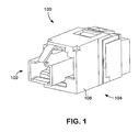
- FIG. 1 is a perspective view of a connector assembly embodying the principles of the present invention
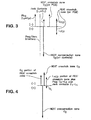
- FIG. 2 is a schematic diagram of the compensation technique to reduce crosstalk in the connector assembly of FIG. 1 ;
- FIG. 3 is a NEXT schematic vector diagram of the connector assembly of FIG. 1 ;
- FIG. 4 is a FEXT schematic vector diagram of the connector assembly of FIG. 1 ;
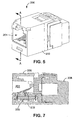
- FIG. 5 is a perspective view of an electrical jack embodying the principles of ' the present invention.
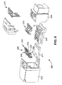
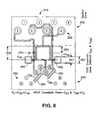
- FIG. 6 is an exploded view of the electrical jack of FIG. 5 ;
- FIG. 7 is a sectional view of the electrical jack of FIG. 5 taken along line AA of FIG. 5 ;
- FIG. 8 is a plan view of the printed circuit board of the electrical jack of FIG. 5 ;
- FIG. 9 is a plan view of an alternative printed circuit board of the electrical jack of FIG. 5 ;
- FIG. 10 is a sectional view of the printed circuit board of FIG. 9 taken along line A-A of FIG. 9 ;
- FIG. 11 is a sectional view of the printed circuit board of FIG. 9 taken along line B-B of FIG. 9 ;
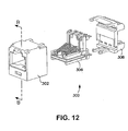
- FIG. 12 is a perspective exploded view of another electrical jack embodying the principles of the present invention.
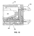
- FIG. 13 is a sectional view of the electrical jack of FIG. 12 taken along line B--B of FIG. 12 .
- FIG. 14 is a perspective view of one embodiment of a flexible circuit capacitor
- FIG. 15 is a bottom view of the flexible circuit capacitors attached to jack contacts, shown in the unformed state
- FIG. 16 is a top view of the flexible circuit capacitor of FIG. 14 ;
- FIG. 17 is a sectional view taken along line C-C of FIG. 16 ;
- FIG. 18 is a sectional view taken along line D-D of FIG. 16 ;
- FIG. 19 is a sectional view taken along line E-E of FIG. 16 ;
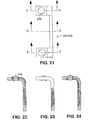
- FIG. 20 is a perspective view of another embodiment of a flexible circuit capacitor
- FIG. 21 is a top view of the flexible circuit capacitor of FIG. 20 ;
- FIG. 22 is a sectional view taken along line F-F of FIG. 21 ;
- FIG. 23 is a sectional view taken along line G-G of FIG. 21 ;
- FIG. 24 is a sectional view taken along line H-H of FIG. 21 ;
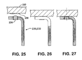
- FIGS. 25-27 are sectional views taken along lines F-F, G-G and H-H, respectively, of FIG. 21 , showing the flexible circuit capacitor being connected to a contact;
- FIG. 28 is a perspective view of a flexible circuit capacitor according to one embodiment of the present invention.
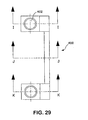
- FIG. 29 is a top view of the flexible circuit capacitor of FIG. 28 ;
- FIG. 30 is a sectional view taken along the line I-I of FIG. 29 ;
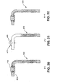
- FIG. 31 is a sectional view taken along the line J-J of FIG. 29 ;
- FIG. 32 is a sectional view taken along the line K-K of FIG. 29 ;
- FIGS. 33-35 are sectional views of a flexible capacitor showing a solder rivet being attached to a jack contact
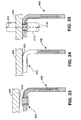
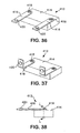
- FIG. 36 is a perspective view of a jack contact capacitor according to one embodiment of the present invention.
- FIG. 37 is a perspective view of a jack contact capacitor with bent contact strips
- FIG. 38 is a side view of the jack contact capacitor of FIG. 36 ;
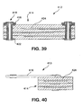
- FIG. 39 is a sectional view taken along the line L-L of FIG. 38 ;
- FIG. 40 is a side cutaway view of the jack contact capacitor of FIG. 36 ;
- FIG. 41 is a side cutaway view showing contact capacitors mounted to jack contacts in a sled in an unmated position
- FIG. 42 is a side cutaway view of the contact capacitors mounted to jack contacts in a sled of FIG. 41 showing the jack contacts in a mated position;
- FIG. 43 is a perspective view of a jack contact capacitor according to one embodiment of the present invention.
- FIG. 44 is a top view of the jack contact capacitor of FIG. 43 ;
- FIG. 45 is a sectional view taken along the line M-M of FIG. 44 ;
- FIG. 46 is a sectional view taken along the line N-N of FIG. 44 ;
- FIG. 47 is a sectional view taken along the line O-O of FIG. 44 ;
- FIG. 48 is a top view of jack contact capacitors attached to jack contacts
- FIG. 49 is a side view of jack contact capacitors attached to jack contacts
- FIG. 50 is a rear view of jack contact capacitors attached to jack contacts
- FIG. 51 is a side cutaway view of jack contact capacitors attached to jack contacts in a sled in an unmated position
- FIG. 52 is a side cutaway view of jack contact capacitors attached to jack contacts in a sled in a mated position
- FIG. 53a is a perspective view showing jack contact capacitors of one embodiment of the present invention mounted to jack contacts;
- FIG. 53b is a perspective view showing jack contact capacitors according to one embodiment of the present invention.
- FIG. 54 is a detail view of the detail "P" of FIG. 53b ;
- FIG. 55 is a side cutaway view showing jack contact capacitors attached to jack contacts mounted to a sled;
- FIG. 56 is a rear view of a jack-and-capacitar assembly according to the embodiment of FIG. 53a ;
- FIG. 57 is a side cutaway view of an adhesive area of a jack contact capacitor connected to a jack contact;
- FIG. 58 is a perspective view of a flexible circuit according to one embodiment of the present invention.
- FIG. 59 is a plan view of a flexible shunt according to one embodiment of the present invention.
- FIG. 60 is a side view of the flexible shunt of FIG. 59 ;
- FIG. 61 is a side view of a flexible shunt mounted between jack contacts and a printed circuit board
- FIG. 62 is a sectional view taken along the line Q-Q of FIG. 59 ;
- FIG. 63 is a perspective view of flexible circuit capacitors according to one embodiment of the present invention.
- FIG. 64 is a detail view of the detail "R" of FIG. 63 ;
- FIG. 65 is a top view of a flexible circuit capacitor of FIG. 63 ;
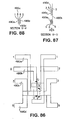
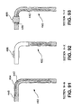
- FIG. 66 is a side view of a flexible circuit capacitor of FIG. 63 ;
- FIG. 67 is a perspective view of a flexible circuit capacitor of FIG. 63 attached to jack contacts;
- FIG. 68 is a perspective view of the flexible circuit capacitors of FIG. 63 attached to jack contacts;
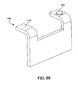
- FIG. 69 is a side view of the flexible circuit capacitors of FIG. 63 attached to jack contacts;
- FIG. 70 is a rear view of the flexible circuit capacitors of FIG. 63 attached to jack contacts;
- FIG. 71 is an end view showing the overlap of capacitive plates in a flexible circuit capacitor of FIG. 63 ;
- FIG. 72 is a plan view showing the overlap of capacitive plates in a flexible circuit capacitor of FIG. 63 ;
- FIG. 73 is a perspective view of a flexible printed circuit according to one embodiment of the present invention.
- FIG. 74 is a plan view of the flexible printed circuit of FIG. 73 ;
- FIG. 75 is a sectional view taken along the line S-S of FIG. 74 ;
- FIG. 76 is a sectional view taken along the line T-T of FIG. 74 ;
- FIGS. 77-80 are plan views respectively showing conductive pathways associated with first, second, third, and fifth conductors of an eight-conductor jack;
- FIGS. 81-84 are perspective views progressively showing conductive pathways of the flexible printed circuit of FIG. 73 ;
- FIG. 85 is a perspective view showing a dielectric layer according to one embodiment of the present invention.
- FIG. 86 is a plan view showing conductive pathways in the flexible printed circuit of FIG. 73 ;
- FIG. 87 is a sectional view taken along the line U-U of FIG. 86 ;
- FIG. 88 is a sectional view taken along the line V-V of FIG. 86 ;
- FIG. 89 is a perspective view of a flexible circuit capacitor according to one embodiment of the present invention.
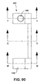
- FIG. 90 is a top view of the flexible circuit capacitor of FIG. 89 ;
- FIG. 91 is a sectional view taken along the line W-W of FIG. 90 ;
- FIG. 92 is a sectional view taken along the line X-X of FIG. 90 ;
- FIG. 93 is a sectional view taken along the line Y-Y of FIG. 90 ;
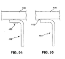
- FIG. 94 is a side view of the flexible circuit capacitor of FIG. 89 showing a rivet attached to a jack contact;
- FIG. 95 is a side view of the flexible circuit capacitor of FIG. 89 showing an adhesive area bonded to a jack contact;
- FIG. 96 is a perspective view of a NEXT compensation capacitor circuit according to one embodiment of the present invention.
- FIG. 97 is a plan view of conductive plates of the NEXT compensation capacitor circuit of FIG. 96 ;
- FIG. 98 is an end view along the view line "Z" of FIG. 97 ;
- FIGS. 99-104 are plan views of the interior of the NEXT compensation capacitor circuit of FIG. 96 showing the shapes of conductive plates;
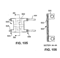
- FIG. 105 is a plan view of a flexible printed circuit according to one embodiment of the present invention.
- FIG. 106 is a sectional view taken along the line AA-AA of FIG. 105 ;
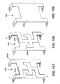
- FIGS. 107-109 are perspective views showing successive layers of the flexible printed circuit of FIG. 105 ;
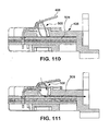
- FIG. 110 is a side cutaway view showing flexible printed circuits of FIG. 105 installed within a jack with jack contacts in an unmated position;
- FIG. 111 is a side cutaway view showing flexible printed circuits of FIG. 105 installed within a jack with jack contacts in a mated position;
- FIG. 112 is a plan view of a flexible printed circuit according to another embodiment of the present invention.
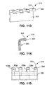
- FIG. 113 is a perspective view of a flexible PCB according to one embodiment of the present invention.
- FIG. 114 is a side view of the flexible PCB of FIG. 113 ;
- FIG. 115 is a front view of the flexible PCB of FIG. 113 ;
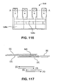
- FIG. 116 is another front view of the flexible PCB of FIG. 113 showing conductive pathways
- FIG. 117 is an end view toward the line A/A of FIG. 116 ;
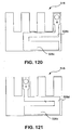
- FIGS. 118-121 are front views of the flexible PCB of FIG. 113 showing, respectively, capacitive plates associated with fifth, third, sixth, and fourth conductors of an eight-conductor jack.
- the communication connector assembly 100 includes a compensation technique that reduces net crosstalk in accordance with the principles of the present invention.
- the communication connector assembly 100 includes a plug 102 that is connectable to a jack 104.
- the jack 104 includes a housing 106 and a carrier portion to hold a printed circuit board (not shown).
- the housing 106 of the jack 104 holds an array of closely spaced parallel contacts for contacting corresponding contacts of the plug 102.
- Crosstalk is primarily generated in the connector assembly due to the closely spaced parallel conductors within the plug 102 and the jack 104. In general, cross-talk is a measure of undesirable signal coupling from one circuit pair to another.
- Near end crosstalk NEXT
- NEXT Near end crosstalk
- NEXT Signal Voltage due to (Capacitive Coupling (C) + Inductive Coupling (L)).
- Far end crosstalk FEXT is a measurement of crosstalk traveling in the same direction as a disturbing signal in a different circuit pair.
- FEXT Signal Voltage due to (Capacitive Coupling (C) - Inductive Coupling (L)).
- FIG 2 The major couplings which illustrate how a preferred embodiment functions are illustrated schematically in FIG 2 :
- the plug is primarily distributed inductive and capacitive coupling.
- the NEXT compensation zone is remote capacitive coupling.
- the jack contacts are primarily distributed inductive and capacitive coupling.
- the NEXT crosstalk zone is remote capacitive coupling.
- the FEXT crosstalk zone is a combination of distributed inductive and capacitive coupling and a remote capacitive coupling.
- NEXT is the reflected signal from any coupling back to the cable connection to the plug.
- the phase angle of each element of NEXT is dependent on the distance from said cable connection to and from said element.
- FEXT is the signal from any coupling that travels to the cable connection to the jack.
- All such signals from distributed couplings are in phase regardless of their location.
- the phase angle of the signal from each remote coupling is, however, dependent on the distance to and from the remote coupling to the current carrying conductors.
- conductors 3,6 form one wire pair and conductors 4,5 form another wire pair. It will be recognized that different wire pair combinations and other wire pairs can be utilized without departing from the spirit and scope of the present invention.
- the compensation scheme of the connector assembly 100 includes a NEXT compensation scheme and a FEXT compensation scheme.
- the NEXT compensation scheme preferably includes a NEXT compensation zone and a NEXT crosstalk zone.
- the NEXT compensation scheme reduces the NEXT of the plug and the jack to effectively zero at a selected null frequency.
- FIG. 3 is a vector representation of the NEXT compensation scheme implemented on the two wire pairs 3,6 and 4,5 according to the present invention.
- the plug 102 of the connector assembly 100 introduces offending NEXT onto the circuit pairs of the connector assembly 100.
- the offending NEXT of the plug 102 includes an inductive component from inductive coupling (Lp) and a capacitive component from capacitive coupling (Cp).
- the NEXT compensation zone of the connector assembly 100 introduces a compensation component from capacitive coupling (C2) on the circuit pairs of the connector.
- the magnitude of the capacitive coupling (C2) is preferably greater than the magnitude of the couplings of the plug (Cp + Lp), but with opposite polarity. In this embodiment, the magnitude of the capacitive coupling (C2) is approximately twice the magnitude of the offending couplings of the jack 104.
- the magnitude of the resultant NEXT is dependent on the magnitude of the phase angle between the coupling of the plug and the capacitive coupling (C2). The larger the phase angle, the larger the resultant NEXT. It is therefore desirable to minimize this phase angle. This phase angle is proportional to the distance between the effective center of the crosstalk coupling of the plug and the effective center of the NEXT compensation zone.
- the NEXT compensation zone introduces a capacitive compensation coupling (C2) on the circuit pairs of the jack to reduce the offending NEXT of the plug.
- C2 capacitive compensation coupling
- the NEXT compensation zone can be implemented in the jack 104 by connecting capacitors between selected jack contacts at or near but on the opposite sides of the electrical interface 110 of the jack 104 contacts and the plug 102 contacts. As a result, the phase angle between the offending NEXT of the plug and the compensation component introduced by the NEXT compensation zone is minimized.
- the capacitors of the NEXT crosstalk zone are connected between circuit paths 3 and 5, and 4 and 6 at or near the electrical interface 110 of the jack contacts and the plug contacts.
- the jack contacts of the connector assembly 100 introduce couplings onto circuit pairs of the connector assembly.
- the couplings of the jack contacts include an inductive component (L1) and a capacitive component (C1).
- the NEXT crosstalk coupling (C3) has the same polarity as the coupling of the plug 102, but has the opposite polarity of the capacitance compensation coupling (C2).
- the NEXT crosstalk zone is located at a particular phase angle at the null frequency from the NEXT compensation zone. In the preferred embodiment, since the phase angle between the coupling of the plug and the capacitive coupling (C2) of the NEXT compensation zone is relatively small, the phase angle between the capacitive coupling (C2) of the NEXT compensation zone and the capacitive coupling (C3) of the NEXT crosstalk zone is relatively small.
- the length of that portion of the jack contacts between the NEXT compensation zone and the NEXT crosstalk zone is relatively small.
- a preferred embodiment disclosed herein minimizes this length, separates them with air as much as feasible, and still provides adequate force between the jack contacts and the contacts of an installed plug.
- the NEXT crosstalk zone introduces the crosstalk coupling (C3) on the circuit paths of the connector.
- the NEXT crosstalk zone is preferably located at a particular phase angle at the null frequency from the cable connection to the plug.
- the NEXT crosstalk zone can be implemented in the jack 104, for example, by connecting capacitors between the input terminals of the printed circuit board (PCB) of the connector assembly 100. It will also be recognized that such capacitors could be connected between the contacts of the jack 104 at the same locations that the NEXT compensation zone capacitors are connected.
- the NEXT crosstalk zone capacitors could alternatively be connected to the jack contacts between the plug/jack contact interface and the cable connection to the jack.
- the crosstalk coupling (C3) of the NEXT crosstalk zone is introduced by capacitors whose leads are connected between circuit paths 3, 4 and 5, 6 at the input terminals of the PCB.
- the FEXT crosstalk zone includes a crosstalk coupling (C C ) and compensation couplings (L FCZ and C L ).
- the location of the effective center of the compensation couplings (L FCZ and C L ) and the effective center of the crosstalk coupling (C C ) of the FEXT crosstalk zone are preferably equidistant and equal in phase angle displacement from the electrical interface of the plug and jack.
- the NEXT components generated by capacitive coupling in the FEXT crosstalk zone are generated by C C and C L and the net of these couplings is C FCZ which is equal to C C -C L .
- the inductive compensation coupling in the FEXT crosstalk zone (L FCZ ) is preferably equal in magnitude and of opposite polarity to the crosstalk component (C FCZ ).
- C FCZ crosstalk component
- couplings C and L for a specification plug both create crosstalk which is designated as negative (-).
- the jack contacts have couplings C and L which both create crosstalk and which are also negative (-).
- NEXT is equal to the signal voltage due to couplings C + L and FEXT is equal to the signal voltage due to couplings C - L.
- the net capacitive coupling of the FEXT crosstalk zone is C FCZ and it is crosstalk and has a negative (-) sign.
- the inductive coupling of the FEXT crosstalk zone is L FCZ and it is compensation and has a positive sign (+).
- the magnitude of the net effect of the FEXT crosstalk zone on FEXT has been derived to be approximately equal to the loss of the net effect of the plug and jack contacts on FEXT compared to their effect on NEXT.
- phase angle displacement between the various elements is equal to two times the distance (in Phase Angle Displacement) from the signal path to the elements.
- these phase angles are relatively small, and therefore the FEXT is relatively small.
- the inductive coupling portion of the FEXT crosstalk zone, L FCZ is created by adjacent current carrying conductors on the PCB. It is not a design objective, but these conductors produce a minimal amount of capacitive coupling in addition to the inductive coupling. Both of these couplings have a polarity which is opposite to that of the couplings in the plug and which has been designated as positive. The designation of this capacitive coupling is C L .
- the main capacitive coupling portion of the FEXT crosstalk zone is created by capacitor plates which are an integral part of the PCB and which are connected by conductors to the current carrying conductors in the above described inductive coupling portion.
- the connecting conductors are connected at a selected location and are of a selected length to insure the phase angle displacement from the plug/jack contact interface is equal for L FCZ and C FCZ .
- the polarity of this capacitive coupling is negative, the same as the couplings in the plug.
- FEXT is the signal from any coupling that travels to the cable connection to the jack.
- all such signals from distributed couplings are in phase regardless of their location.
- the phase angle of the signal from each remote coupling is, however, dependent on the distance to and from the remote coupling to the current carrying conductors.
- the net plug vector is reduced in magnitude.
- the net jack contact vector is reduced in magnitude.
- the three components of the FEXT crosstalk zone no longer add up to zero. They are now effective.
- all the distributed couplings are in phase with each other and all the remote couplings have a phase angle which is lagging the distributed couplings.
- the FEXT crosstalk zone can be implemented in the printed circuit board of the jack by connecting selected magnitudes of capacitance between circuit paths and by creating mutual inductance between adjacent circuit paths.
- the inductive couplings of the FEXT crosstalk zone are generated in the printed circuit board by positioning circuit paths 3 and 5 in close proximity to each other for a selected distance, and positioning circuit paths 4 and 6 in close proximity to each other for a selected distance.
- capacitors are connected between pairs 3,6 and 4,5 at a selected distance from the input terminals of the printed circuit board.
- the NEXT generated by the FEXT crosstalk zone is self-canceling as described above.
- the effects of couplings on FEXT are determined by distributed couplings and by remote couplings in the same manner regardless of their positioning along signal paths. Therefore, the FEXT crosstalk zone can be positioned at any suitable distance from the NEXT compensation zone, without degrading NEXT or FEXT performance.
- the plug is a specification plug which must be used and it contains inductive and capacitive coupling.
- the contacts are designed to be short in length and mechanically sound. The result is that they contain inductive and capacitive crosstalk coupling. Longer and more complicated contacts could be designed to have minimal inductive coupling or inductive compensation coupling however such complications would not enhance the superior results of this invention.
- the NEXT compensation zone design provides the minimum phase angle change from the interface of the plug/jack contacts to the effective center of the NEXT compensation zone.
- the NEXT compensation zone coupling is all capacitive because simple alternate designs with inductive coupling would increase the phase angle change.
- the NEXT compensation zone design allows minimum NEXT to be achieved and it is one of the most important elements of this invention.
- the NEXT crosstalk zone provides only capacitive coupling. This is the optimum design because it provides the required balance to minimize NEXT and it has no detrimental affect on FEXT.
- the FEXT crosstalk zone is also one of the most important elements of this invention and in combination with the unique compensation zone, the synergy results in a very important technical achievement.
- the parameters of the FEXT crosstalk zone design provided herein results in a relatively small FEXT; however, it is contemplated that the FEXT could be reduced further by changing design parameters.
- C L which could be achieved by locating conductor 3 above 5 instead or adjacent to it and by locating conductor 6 above 4 instead of adjacent to it.
- C L With C L increased, C C would necessarily be increased. Since the phase angle of C C is more nearly 180° from the NEXT compensation zone C2 than C C , FEXT would be reduced.
- Another example is to increase the length of conductors 3,5 and 4,6 in combination with separating them to keep L FCZ the same. Since C C must be in the center of the FEXT crosstalk zone, the distance from the current paths to the remote Cc would necessarily be increased and this would change its phase angle which could be made optimum.
- the parameters of the components of the compensation scheme implemented by the connector assembly are provided as follows:
- the values of the components of the compensation scheme may be varied in magnitude about their initially determined values for purposes of fine tuning.
- the embodiment has been applied to pairs 3,6 and 4,5 of a connector assembly, it will be recognized that the principles described herein can be applied to other pair combinations of an electrical connector, such as a jack.
- the electrical connector is preferably a jack 200.
- the jack 200 minimizes the phase angle delay for introducing crosstalk compensation by introducing it at the plug/jack contact interface where the offending crosstalk is introduced to a jack by a mating plug (not shown).
- the jack 200 includes a housing 202 defining a plug receiving opening 204, a PCB and conductor carrying sled 206 and a wire containment cap 208.
- the jack 200 is an 8 contact type (i.e., 4 twisted pair) connector arrangement according to a wire pair industry standard (i.e., wires 4 and 5 comprising pair 1, wires 3 and 6 comprising pair 2, wires 1 and 2 comprising pair 3, and wires 7 and 8 comprising pair 4). It is contemplated that the jack can be any other type of suitable jack or connector.
- the contact carrier 206 of the jack 200 includes a printed circuit board (PCB) 210 and a plurality of contacts 220.
- the contacts 220 each have a first end portion 222 fixedly attached to the printed circuit board 210 and a second free end portion 224.
- Each contact 220 also has a contact portion 226 extending between its first and second end portions 222, 224.
- the plug introduces offending NEXT onto the jack conductors at the electrical interface of the contacts 220 and the plug.
- the jack 200 introduces a capacitive compensation coupling (C2) at said electrical interface.
- the capacitance compensation coupling (C2) of the NEXT compensation zone is preferably provided by flexible printed circuit capacitors 230 and 232 that are connected with flexible arms to the underside of the contact portions 226 of the contacts 220.
- the capacitors 230 and 232 are connected across contacts 220 associated with wire pair 1 (wires 3 and 5) and wire pair 2 (wires 4 and 6).
- the capacitors 230 and 232 are installed by electrically connecting flexible printed circuit capacitive plates to the respective contacts 220. It will be recognized that the capacitors can be implemented by any suitable capacitive element. Since the capacitance compensation component (C2) is connected at said plug/jack contact interface and since the distance from said plug/jack contact interface to the effective center of the capacitors is minimized, the phase angle between the offending NEXT of the plug and the NEXT compensation coupling (C2) is minimized.
- the printed circuit board 210 has a front portion 250 and a rear portion 252.
- the front portion 250 includes a plurality of front terminals 260 labeled 1-8 and the rear portion 252 of the printed circuit board 210 includes a plurality of rear terminals 262 labeled 1-8.
- the front terminals 260 labeled 3-6
- the rear terminals 262 labeled 3-6
- Insulation displacement contacts (IDCs) 270 are mounted to each of the rear terminals 262 as shown in FIG. 6 .
- the IDCs 270 are electrically connected through the circuit paths on the printed circuit board 210 to the front terminals 260.
- the jack 200 introduces a crosstalk or reverse compensation coupling (C3) at specific locations on the circuit paths of the connector 200 at the NEXT crosstalk zone.
- the capacitance compensation component C3 of the NEXT crosstalk zone of the jack 200 is introduced by capacitors 280 and 282 as shown in FIG. 8 .
- the capacitors 280 and 282 are connected across front terminals 3, 4 and terminals 5, 6, respectively, of the printed circuit board 210 of the jack 200 and are preferably formed by parallel conductive plates. It will be recognized that the capacitors 280 and 282 can be discrete components, such as a capacitor, or any other suitable capacitive element. For example, the capacitors can be formed on the same or different layers of the circuit board and the shape or type of the capacitors can be varied.
- the printed circuit board 210 of the jack 200 implements a FEXT crosstalk scheme or zone to reduce or cancel the FEXT of the plug/jack combination.
- the FEXT compensation scheme introduces a crosstalk capacitive coupling (C C ) and inductive and capacitive compensation couplings (L FCZ and C L ) onto the circuit paths of the printed circuit board 210.
- the capacitance compensation coupling C C of the FEXT crosstalk zone is introduced by capacitors 290 and 292, and the compensation couplings (L FCZ and C L ) are created by positioning the current carrying circuit paths in close proximity to each other. It is to be noted that the thickness or the cross-sectional dimension of the traces as well as the distance or spacing between the conductors or traces can also be adjusted to achieve the required couplings.
- the capacitors 290 and 292 are connected across terminals 3, 5 and 4, 6, respectively, near the front terminals of the printed circuit board 210 of the jack 200.
- Each of capacitors 290 and 292 are preferably formed by parallel conductive plates, but can be implemented by any suitable capacitor element.
- the locations of the effective center of the compensation couplings (L FCZ and C L ) and the effective center of the capacitance crosstalk coupling (C C ) of the crosstalk zone are preferably equidistant and equal in phase angle displacement from the electrical interface of the plug and jack.
- the generation of the inductive compensation coupling (L FCZ ) introduces a capacitive coupling (C L ) having the same polarity as the inductive coupling (L FCZ ).
- the magnitude of the compensation coupling (C C ) is designed to cancel the C L coupling out as well as the inductive coupling (L FCZ ) in the generation of NEXT.
- C FCZ C C -C L .
- the compensation couplings (L FCZ and C L ) are preferably equal in magnitude and of opposite polarity to the crosstalk component (C C ). Therefore, the two components (L FCZ ) and (C FCZ ) will cancel each out in the generation of NEXT.
- the IDCs have been designed so their effect on NEXT and FEXT is minimal. Their effect has been ignored.
- the layout illustrated in FIG. 8 is effective in compensating for forward FEXT without adversely affecting forward NEXT (i.e. NEXT observed when the driven signal is received from the cable connection to the plug). Because the effective center of the compensation couplings (L FCZ and C L ) and the effective center of the capacitance crosstalk coupling (C C ) of the crosstalk zone are designed to be equidistant from the electrical interface of the plug and jack, the resultant inductive and capacitive coupling vectors of the FEXT crosstalk zone are at the same phase angle location with regard to their effect on forward NEXT.
- FIG. 9 is a plan view of a layout for an alternative PCB 550 having couplings that are symmetrical from either direction, thereby providing FEXT compensation without adversely affecting forward or reverse NEXT.
- the PCB 550 includes a front portion 552 and a rear portion 554.
- the front portion 552 includes a plurality of front terminals 560 labeled 1-8 and the rear portion 554 includes a plurality of rear terminals 562 labeled 1-8.
- FIG. 8 only the circuit pathways between front terminals (labeled 3-6) and rear terminals (labeled 3-6) are shown.
- the NEXT crosstalk zone has been omitted from FIG. 9 for clarity.
- the FEXT crosstalk zone of PCB 550 utilizes distributed inductive couplings (i.e. where traces are placed in close horizontal or vertical proximity to one another).
- the PCB 550 utilizes distributed capacitive couplings 590, which take the form of partially overlapping traces widened to approximate distributed parallel plates.
- the coupling vectors are at the same phase angle location with regard to their effect on both forward and reverse NEXT.
- the FEXT compensation zone benefits FEXT while being neutral to both forward and reverse NEXT.
- FIGS. 10 and 11 are sectional views of the PCB 550 taken along lines A--A and B--B, respectively, of FIG. 9 .
- the traces corresponding to traces 3, 4, 5, and 6 are shown to each traverse one of four internal layers of the PCB 550. This stratification provides spacing for desired capacitive and inductive coupling effects to appropriate FEXT compensation.
- FIGS. 9-11 illustrate one possible implementation of a symmetrical FEXT compensation zone
- other implementations may also be used without departing from the intended scope of the invention.
- different lengths and arrangements of traces may be used.
- different shapes and configurations for distributed capacitances may be adopted.
- FIGS. 12 and 13 another electrical connector 300 implementing the same compensation scheme to reduce NEXT and FEXT according to the present invention is shown.
- the electrical connector 300 is substantially similar to the previously described electrical connector 200, except that the connection arrangement between the jack and the cable to which it is connected to is a "punch down" design.
- Components of the electrical connector 300 which generally correspond to those components of the electrical connector 200 of FIG. 5 are designated in the three-hundred series. As such, further description of the electrical connector 300 is unnecessary for a complete understanding of the present invention.
- the method and apparatus of the present invention provide a compensation technique to cancel or reduce the NEXT and FEXT produced by the electrical connector.
- the compensation scheme introduces compensation and crosstalk couplings into the electrical paths of the electrical connector to reduce or cancel the net crosstalk generated by the plug/jack combination.
- the capacitors 230 and 232 are connected across contacts 220 associated with wire pair 1 (wires 3 and 5) and wire pair 2 (wires 4 and 6).
- the capacitors 230 and 232 are installed by electrically connecting flexible printed circuit capacitive plates to the respective contacts 220. It will be recognized that the capacitors can be implemented by any suitable capacitive element. Since the capacitance compensation component (C 2 ) is connected at said interface and since the distance from said interface to the effective center of the capacitors is minimized, the phase angle between the offending NEXT of the plug and the NEXT compensation coupling (C 2 ) is minimized.
- FIGS. 14-19 illustrate one embodiment of the flexible printed circuit capacitors.
- These flexible circuit capacitors are made, for example, from a plated film of KAPTON® polyimide film manufactured by DuPont.
- the capacitors 230 and 232 include a pair of dome-shaped rivets and are attached opposite the plug/jack contact interface via electrical resistance or spot welding.
- FIGS. 20-27 illustrate a second embodiment of the flexible printed circuit capacitors 230 and 232. These capacitors include a solder "plug" 236 and are attached to the contacts 220 that may include a pre-tinned area 238.
- FIGS. 28-121 illustrate additional embodiments of capacitors according to the present invention.
- FIG. 28 shows a flexible circuit capacitor 400 having solder rivets 402.
- the solder rivets 402 are pre-formed and mechanically deformed into holes provided at the ends of the capacitor 400.
- the flexible circuit capacitor 400 attaches to jack contacts by a resistance weld process.
- FIG. 29 is a top view of the flexible circuit capacitor 400, and FIGS. 30, 31 , and 32 are, respectively, cross-sectional views taken along the lines I-I, J-J, and K-K of FIG. 29 .
- the solder rivet 402 is inserted in a plated through hole 404.
- the plated through hole 404 is provided with pads.
- the rivet 402 has a dome head 406 (shown in FIG. 31 ), and the rivet 402 is mechanically deformed on the underside as shown in FIGS. 30 and 32 .
- FIGS. 33 , 34 , and 35 are cross-sectional views of a flexible circuit capacitor 400 with a solder rivet 402 being attached to a jack contact 408.
- the jack contact 408 may be provided with a pre-tinned region 410 tinned with solder.
- the flexible circuit capacitor 400 is brought together with the jack contact 408 as shown in FIG. 34 so that the solder rivet 402 makes physical contact with the pre-tinned region 410.
- a welding tool 412 welds the rivet 402 to the contact 408, for example by resistance welding. The welding may be performed simultaneously on several rivet-contact interfaces.
- the centerline 412c shown in FIG. 35 is preferably located at the plug/jack contact interface.
- FIG. 36 shows an alternative PCB-type jack contact capacitor 413.
- the jack contact capacitor 413 can serve as a NEXT compensation zone.
- a printed circuit board 414 has contact strips 416 attached to it at eyelets 418.
- Contact mating areas 420 are also provided on the contact strips 416 for attachment, for example via welding, to contacts of a jack.
- FIG. 37 A similar construction is shown in FIG. 37 , with the contact strips 416 bent for alternative mounting of the contact capacitor to a contact.
- FIG. 38 is a side view of the jack contact capacitor 413 of FIG. 36
- FIG. 39 is a cross-sectional view taken along the line L-L of FIG. 38 .
- FIG. 39 shows the contact strip 416 held in place by the eyelet 418 and in electrical contact with a plated through hole 422.
- Conductors 424 are also in contact with the plated through hole 422 and allow capacitive coupling between contact strips 416 within a printed circuit board 414.
- FIG. 40 shows a side cutaway view illustrating varying widths of the conductors 424 within the printed circuit board 414.
- FIGS. 41 and 42 are side views of contact capacitors mounted to jack contacts 408 provided in a sled 426.
- the printed circuit boards 414 of the jack contact capacitors fit within capacitor guides 428 of the sled 426.
- a sled-mounted printed circuit board 430 may be provided within the sled 426.
- FIG. 41 shows the jack contacts 408 not mated to a plug and
- FIG. 42 shows the jack contacts 408 bent downwardly as they would be bent when mated to a plug.
- a centerline 430c shows the plug/jack contact interface.
- the contact strips 416 are welded to the contacts 408 directly beneath the plug/jack contact interface, along the centerline 430c.
- FIG. 43 another embodiment of a jack contact capacitor 432 for implementing a NEXT compensation zone is shown.
- a flexible printed circuit 434 is adapted for connection to jack contacts via rivets 436a and 436b.
- the rivets 436a and 436b are preferably provided with domed heads.
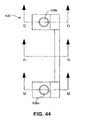
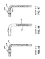
- FIG. 44 is a top view of the jack contact capacitor 432, and FIGS. 45-47 are, respectively, cross-sectional views taken along the lines M-M, N-N, and O-O of FIG. 44 .
- a plated through hole 438 allows for electrical connection between a first rivet 436a and a first conductive plate 440. Further, as shown in FIG.
- FIG. 46 shows a cross-sectional view of a region of capacitive coupling between the first conductive plate 440 and the second conductive plate 442.
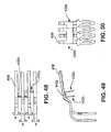
- FIGS. 48-50 show jack contact capacitors 432a and 432b attached to jack contacts 408.
- FIG. 48 is a top view of jack contacts 408 attached to jack contact capacitors 432a and 432b
- FIG. 49 is a side view of the assembly of FIG. 48
- FIG. 50 is a rear view of the assembly of FIG. 48 .
- Contacts 3, 4, 5, and 6 of an eight-contact jack are shown.
- a centerline 442c of the welding between the jack contacts 408 and the jack contact capacitors 432a and 432b aligns with a plug/jack contact interface.
- the jack contact capacitors 432a and 432b are welded to the jack contacts 408 at a side opposite the plug/jack contact interface.
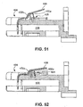
- Jack contact capacitors 432a and 432b can be attached to jack contacts 408 and mounted within a sled 426 as shown in FIGS. 51 and 52.
- FIG. 51 shows the position of jack contacts 408 when a plug is not mated to the jack contacts 408 and
- FIG. 52 shows the position of jack contacts mated with a plug.
- a printed circuit board 430 may be provided within the sled 426.
- Capacitor guides 428 are positioned to accept the jack contact capacitors 432a and 432b.
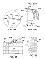
- FIGS. 53a -56 Another embodiment of a jack contact capacitor is shown in FIGS. 53a -56 .
- jack contact capacitors 444a and 444b are adhesively mounted to jack contacts 408.
- FIG. 53a shows jack contact capacitors 444a and 444b mounted to jack contacts 408.
- Jack contacts 3, 4, 5, and 6 of an eight-contact jack are shown.
- FIG. 53b shows the jack contact capacitors 444a and 444b separated from the jack contacts 408, and
- FIG. 54 is a detail view of the detail "P" of FIG. 53b .
- adhesive areas 446 are provided on contact strips 416 of the jack contact capacitors 444a and 444b.
- FIG. 56 is a rear view of a jack-and-capacitor assembly according to this embodiment of the invention.
- the jack contact capacitors 444a and 444b are formed with flexible printed circuits 448, as shown in FIG. 54 .
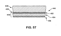
- FIG. 57 shows a side cutaway view of an adhesive area 446 of a jack contact capacitor 444 connected to a jack contact 408.
- Adhesive 450 is placed between a first dielectric layer 452, such as a layer of MYLAR® PET film manufactured by DuPont, and a jack contact 408.
- a conductor pattern 454 is layered between the first dielectric layer 452 and a second dielectric layer 456. The conductor pattern 454 is layered between the first and second dielectric layers 452 and 456 in a flexible printed circuit 448.
- the jack contact capacitors 444a and 444b are adhesively bonded to alternate jack contacts.
- jack contact capacitor 444a may be bonded to jack contact pair 3-5 and jack contact capacitor 444b may be bonded to jack contact pair 4-6.
- This construction creates a capacitor by means of the conductor material 454 in the laminate form and the contact 408 itself. Two contacts are then coupled by two capacitors in series. Total capacitance between contacts is 1 ⁇ 2 the value of each capacitor. The thickness and dielectric of the adhesive is included in the calculations.
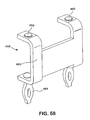
- FIGS. 58-61 show a NEXT compensation zone and flexible circuit contact shunt according to one embodiment of the present invention.
- a flexible NEXT compensation circuit 458 comprises a capacitor flexible circuit 460 adapted to connect to jack contacts via contact weld rivets 462 and further adapted to make electrical contact with a printed circuit board via printed-circuit-board compliant pins 464. In the embodiment shown in FIG. 58 , capacitive coupling between two contacts may be accomplished within a capacitor flexible circuit 460.
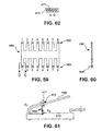
- FIG. 59 a flexible shunt 466 is shown. The flexible shunt 466 is provided with rivets 462 for connection to jack contacts and with PCB-compliant pins 464 for connection to a printed circuit board.
- FIG. 60 A side view of the flexible shunt 466 is shown in FIG. 60.
- FIG. 61 is a side view illustrating the placement of a flexible shunt 466 between jack contacts 468 and a printed circuit board 470. A segment of a plug 471 is shown, and the plug/jack contact interface 473 is directly above the location of attachment of the rivets 462 to the jack contacts 468.
- FIG. 62 is a cross-sectional view of the flexible shunt 466 along the line Q-Q of FIG. 59 .
- a conductive trace 472, such as a copper trace, is surrounded by a dielectric 474 such as KAPTON® polyimide film manufactured by DuPont.
- FIGS. 59-62 show a flexible shunt 466 providing electrical connection only, with no capacitor plates.
- the use of a flexible circuit shortens the current path from the plug 471 to the printed circuit board 470.
- the signal length x 2 shown in FIG. 61 is less than the signal length x 1 .
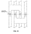
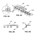
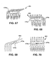
- FIGS. 63-72 show an alternative flexible circuit capacitor 476 for implementing a NEXT compensation zone.
- FIG. 63 is a perspective view of two flexible circuit capacitors 476a and 476b having domed rivets 478 for attachment to first through eighth jack contacts as labeled in FIG. 63.
- FIG. 64 is a detail view of the detail "R" of FIG. 63 showing a domed rivet 478 adapted for welded attachment to a jack contact and a plated through hole 480 for establishing electrical connection between a jack contact and capacitive plates 482, shown as dotted lines in FIG. 63.
- FIG. 65 is a top view of the flexible circuit capacitor 476 more clearly showing the arrangement of the capacitive plates 482 and FIG. 65 is a side view of the flexible circuit capacitor 476, showing a 90° bend 475.
- FIG. 67 is a perspective view showing a flexible circuit capacitor 476a attached to four jack contacts 484.
- FIG. 68 is another perspective view, showing an additional flexible circuit capacitor 476b attached to the other four jack contacts 484.
- the two flexible circuit capacitors 476a and 476b partially overlap each other.
- FIGS. 69 and 70 are respectively side and rear views showing the flexible circuit capacitors 476a and 476b attached to the jack contacts 484.
- a first flexible circuit capacitor 476a is attached to first, second, third, and fifth jack contacts 484, and a second flexible circuit capacitor 476b is attached to fourth, sixth, seventh, and eighth jack contacts 484 as shown in FIGS. 68 and 70 .
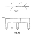
- FIGS. 71 and 72 show the overlap of capacitive plates within a flexible circuit capacitor 476.
- FIGS. 71 and 72 show the flexible circuit capacitor for connection to first, second, third, and fifth jack contacts; the capacitors connected to eighth, seventh, sixth, and fourth contacts are a mirror image of the illustrated capacitors. All pair combinations except for 1,2-7,8 are included.
- the flexible circuit capacitors 476a and 476b are welded to the bottom of jack contacts directly below the plug/jack contact interface.
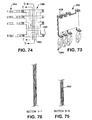
- FIG. 73 is a perspective view of a flexible printed circuit 486 with rivets 488 for connection to jack contacts and printed-circuit-board compliant pins 464 for connection to a printed circuit board.
- the flexible printed circuit 486 can flex between jack contacts and a printed circuit board when a plug is mated to jack contacts, and the rivets 488 are welded directly beneath a plug/jack contact interface.
- FIG. 74 is a plan view of a flexible printed circuit 486 showing conductive pathways 490 with dotted lines.
- a flexible printed circuit 486 for providing a NEXT compensation zone for conductors 1, 2, 3, and 5 is shown; a flexible printed circuit for providing a NEXT compensation zone for conductors 4, 6, 7, and 8 is a mirror image of the shown flexible printed circuit 486.
- Conductive pathways 490 are provided within the flexible printed circuit 486 such that the flexible printed circuit 486 provides both capacitive and inductive NEXT compensation on all conductor pairs except 1,2-7,8.
- FIG. 75 is a cross-sectional view along the line S-S of FIG. 74 and FIG. 76 is a cross-sectional view along the line T-T of FIG. 74 . These views show the positioning of conductive pathways 490 along first and second cross-sections of the flexible printed circuit 486.
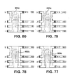
- FIGS. 77-80 are plan views respectively showing in solid lines the conductive pathways 490a-490d associated with first, second, third, and fifth conductors of an eight-conductor jack.
- FIGS. 81-84 progressively show conductive pathways 490 of the flexible printed circuit 486 as printed on the flexible printed circuit 486 from the lowermost to the uppermost conductive pathway.
- FIG. 81 shows the lowermost conductive pathway 490b associated with the second conductor.
- FIG. 82 shows the second lowermost conductive pathway 490d associated with the fifth conductor.
- FIG. 83 shows the second uppermost conductive pathway 490c associated with the third conductor.
- FIG. 84 shows the uppermost conductive pathway 490a associated with the first conductor.
- FIG. 85 shows a dielectric layer 474 such as a layer of Kapton polyimide film manufactured by DuPont.
- the flexible circuit 486 is formed by overlapping these layers.
- FIG. 86 is another plan view of the conductive pathways 490a-490d
- FIGS. 87 and 88 are respectively cutaway views along the lines U-U and V-V of FIG. 86 showing the overlapping of the conductive pathways 490a-d.
- Capacitive plates for the first conductor adjacent capacitive plates for the third conductor and capacitive plates for the second conductor adjacent capacitive plates for the fifth conductor may be added as required.
- FIG. 89 is a perspective view of a flexible circuit capacitor 492 adapted for both welding and adhesive attachment to jack contacts.
- a rivet 488 is provided for attachment to one jack contact and an adhesive area 446 is provided for attachment to another jack contact.
- FIG. 90 is a top view of the flexible circuit capacitor 492, and FIGS. 91-93 are, respectively, cross-sectional views of the flexible circuit capacitor 492 taken along the lines W-W, X-X, and Y-Y of FIG. 90 .
- a flexible dielectric material 494 overlays first and second conductive plates 440 and 442. The adhesive area 446 is shown in FIG.
- FIG. 94 is a side view showing the rivet 488 welded to a jack contact 408
- FIG. 95 is a side view of the adhesive area 446 bonded to a jack contact 408.
- capacitive coupling between the jack contact 408 and the flexible circuit capacitor 492 occurs at the adhesive bond area. Both the weld and the adhesive bond are placed directly beneath a plug/jack contact interface.
- FIGS. 96-104 a NEXT compensation capacitor circuit 496 for connection to all eight conductors of an eight-conductor jack is illustrated.
- the NEXT compensation capacitor circuit 496 is a flexible capacitor circuit.
- FIG. 96 is a perspective view of a NEXT compensation capacitor circuit 496. Rivets 497 are provided for welding to the bottoms of jack contacts at plug/jack contact interfaces.
- FIG. 97 is a plan view of conductive plates 498 associated with each of the eight contacts of a jack. The association between conductive plates 498a-498h with the respective first through eighth contacts is shown in FIG. 98 , which is a side view along the view line Z of FIG. 97 showing the overlap of the conductive plates 498a-498h.
- FIGS. 99-104 are plan views of the interior of the NEXT compensation capacitor circuit 496 showing the shapes of conductive plates 498a-498h.
- FIGS. 99-104 progress from FIG. 99 which shows the lowermost conductive plate 498a of FIG. 98 (associated with a first jack contact) to FIG. 104 which shows the uppermost conductive plate 498h of FIG. 98 (associated with an eighth jack contact).
- FIGS. 105-109 illustrate another flexible printed circuit 500 with capacitive and inductive NEXT compensation for attachment to contacts of a jack.
- FIG. 105 is a plan view of the flexible printed circuit 500 with dotted lines showing conductive pathways 502.
- a first end 504 of the flexible printed circuit 500 is attached to jack contacts via weld/solder pads 505 and a second end 506 is attached to a printed circuit board via PCB-compliant pins 464.
- the flexible printed circuit 500 is adapted for use with third and fifth contacts of an eight-contact jack; an identical flexible printed circuit 500 can also be used with fourth and sixth contacts.
- FIGS. 107-109 show successive layers of the flexible printed circuit 500.
- FIG. 107 shows a first dielectric layer 508a and a first conductive pathway 502a associated with a third jack contact.
- FIG. 108 shows a second dielectric layer 508b and a second conductive pathway 502b associated with a fifth jack contact.
- FIG. 109 shows a third dielectric layer 508c.
- the dielectric layers 508a-c may be comprised of KAPTON®.
- FIGS. 110 and 111 show flexible printed circuits 500 installed within a jack.
- Jack contacts 408 are mounted within a sled 426 and the flexible printed circuits 500 are welded to the jack contacts 408 beneath a plug/jack contact interface.
- the flexible printed circuits 500 are soldered to a PCB 509.
- FIG. 110 shows the jack contacts 408 in a position in which they are not mated to a plug
- FIG. 111 shows the jack contacts 408 in a position in which they are mated to a plug.
- the flexible printed circuits 500 flex as the jack contacts 408 move between the two positions.
- the arrows of FIG. 111 show a current path through the jack including the paths through the flexible printed circuits 500.
- FIG. 112 is a plan view of another flexible printed circuit 510 for providing capacitive and inductive NEXT compensation. Rivets 511 are provided for attachment to jack contacts.
- the flexible printed circuit 510 of FIG. 112 is adapted for attachment to third and fifth jack contacts, but a substantially identical flexible printed circuit can be used for attachment to fourth and sixth jack contacts of an eight-contact jack.
- Conductive pathways 512a and 512b are provided within the flexible printed circuit 510, and capacitor plates 514a and 514b are attached to each of the conductive pathways 512a and 512b.
- the vertical runs of the conductive pathways 512a and 512b are parallel but not collinear.
- Inductive segments 516a and 516b make up a portion of the vertical runs.
- the inductive segments 516a and 516b are adjacent current carrying conductors and/or transformers providing inductive compensation coupling.
- FIG. 113 is an upper right-side perspective view
- FIG. 114 is a side view
- FIG. 115 is a front elevational view of one embodiment of a flexible PCB 518 that may be utilized in accordance with the present invention to provide crosstalk compensation.
- the PCB 518 includes a main portion 520 and attachment fingers, such as the finger 522.
- the main portion 520 supports a plurality of capacitive plates (in this case, four plates, corresponding to plug interface contacts 3-6) to provide capacitive coupling.
- the leads to the capacitive plates provide an inductive coupling component as well.
- the fingers 522 serve as an attachment mechanism for attaching the PCB 518 to the plug interface contacts.
- a resistance weld rivet 524 is used.
- the rivet 524 acts as a contact post for the capacitive plates and their leads. This is illustrated in FIGS. 114-121 , which show four layers of capacitive plates 526 and leads (528a-d), through which the rivet 524 protrudes to make appropriate contact in the fingers 522.
- FIG. 116 is a front elevational view of the PCB 518 with the fingers in an unbent configuration, for ease of illustration.
- FIG. 117 is a cross-sectional view of the capacitive plates and leads as viewed upward from the bottom of the PCB 518 toward line A/A in FIG. 116 .
- Fig. 114 does not show portions of the PCB 518 that merely support the capacitive plates and leads or serve as a dielectric or insulator.
- FIGS. 116-121 show how the capacitive plates and leads are placed with respect to one another to result in a relatively high density of inductive coupling in a relatively short distance. For example, in FIG.
- the capacitive plate 526a and lead 528a for conductor 5 is the topmost plate and lead shown, having a sideways "U" shape. The same "U" shape, but with varying orientation, is used for conductors 3, 4, and 6, as shown by the dashed and solid lines of FIG. 116 .
- the physical placement and overlapping area of the capacitive plates determines the amount of capacitive coupling. Similarly, the separation of the leads from one another and the length of overlap determine the amount of inductive coupling.
- FIG. 117 also illustrates the relative direction of current flow due to inductive couplings in the respective leads, which provides a high density of inductive coupling.
- FIGS. 118-121 show, respectively, leads 528a-d and capacitive plates 526a-d associated with, respectively, fifth, third, sixth, and fourth conductors of an eight-conductor jack.
- a communication jack configured to receive a plug to form a communication connection, comprising: a plurality of jack contacts, which consist of metal cantilever beams, disposed in the jack, wherein each contact has at least a first surface and a second surface, wherein, upon the plug being received by the jack, a plurality of plug contacts interface with the first surface of the plurality of jack contacts; and a first capacitive coupling connected between two pairs of the plurality of jack contacts to compensate for near end crosstalk, wherein the first capacitive coupling is connected to the pairs of jack contacts along the second surface adjacent to where the plug contacts interface with the jack contacts.
- the first capacitive coupling is located on a first printed circuit board attached to the jack contacts with flexible electrical conductors.
- the first printed circuit board is flexible, allowing it to change shape upon insertion of the plug into the jack; or the first printed circuit board is attached to the second surface by welds, or the first printed circuit board is attached to the second surface by solder plugs, and preferably wherein at least a portion of the jack contacts is pre-tinned for soldering.
- the plug has an associated plug coupling having capacitive and inductive components, and wherein, at a first frequency, the first capacitive coupling is greater in magnitude than the plug coupling, but approximately opposite in polarity, and preferably the first frequency the first capacitive coupling has a magnitude approximately twice that of the plug coupling.
- the first capacitive coupling is connected to the jack contacts directly opposite where the plug contacts interface with the jack contacts.
- the first capacitive coupling is connected between circuit paths 3: 5 and 4: 6 of the jack.
- the communication jack further comprises a second capacitive coupling in electrical contact with the jack contacts, and preferably the plug has an associated plug coupling having capacitive and inductive components, and wherein the second capacitive coupling is approximately opposite in polarity to the first capacitive coupling and approximately identical in polarity to the plug coupling, or an electrical current path from the first capacitive coupling to where the plug contacts interface with the jack contacts is shorter than an electrical current path from the second capacitive coupling to where the plug contacts interface with the jack contacts, or the first capacitive coupling is connected between circuit paths 3: 5 and 4: 6 of the jack, and the second capacitive coupling is connected between circuit paths 3 : 4 and 5: 6 of the jack.
- the communication jack further comprises a far end crosstalk compensation zone comprising inductive and conductive trace patterns on a printed circuit board.
- a crosstalk compensation apparatus for a communication connector consisting of a jack and a plug, comprising a printed circuit that is mechanically and electrically connected to jack contacts by flexible members, each of which is attached on the opposite side of and adjacent to an interface between a jack contact and a corresponding contact of an installed plug, wherein the jack contacts consist of metal cantilever beams.
- the crosstalk compensation apparatus further comprises a Near End Crosstalk (NEXT) compensation zone or the printed circuit is a flexible printed circuit, or the printed circuit provides at least a segment of a network signal path to connectors connecting the jack to a network cable, and preferably the printed circuit provides capacitive compensation; or the printed circuit provides capacitive and inductive compensation.
- NXT Near End Crosstalk
- a crosstalk compensation apparatus for a jack/plug combination which includes a Far End Crosstalk (FEXT) zone wherein the net inductive and capacitive couplings are approximately equal in magnitude and of opposite polarity, and preferably the net capacitive coupling includes both distributed and remote capacitive coupling.
- FXT Far End Crosstalk
- a crosstalk compensation apparatus for a communication connector consisting of a jack and a plug, comprising a Far End Crosstalk (FEXT) zone which has virtually no effect on Near End Crosstalk (NEXT) but which reduces Far End Crosstalk (FEXT).
- FEXT Far End Crosstalk
- a communication jack configured to receive a plug to form a communication connection, comprising: a plurality of jack contacts which consist of metal cantilever beams disposed in the jack, wherein, upon the plug being received by the jack, a plurality of plug contacts interface with a first surface of the plurality of jack contacts at a plug/jack interface; electrical conductors which are mechanically and electrically connected to a second surface of the jack contacts on the opposite side of and adjacent to the plug/jack interface; and crosstalk compensation components connected to the electrical conductors.
- the crosstalk compensation components provide capacitive coupling, and preferably the capacitive coupling is adjacent to the jack contacts or, preferably according to said another alternative embodiment the electrical conductors carry the communication signal current of the plug contact to which they are electrically connected, and preferably the electrical conductors are bent adjacent to where they are connected to the jack contacts and become oriented in a direction which is diverging from the plane that includes the jack contacts at the plug/jack interface; or the electrical conductors are electrically connected to connectors to which an electrical communication cable is connected, or the only communication signal current that is conducted by the jack contacts is approximately normal to a plane that includes the jack contacts at the plug/jack interface, or the crosstalk compensation components include both capacitive and inductive couplings, and preferably wherein the couplings are adjacent to where the electrical conductors connect to the jack contacts.
- a communication jack comprising crosstalk compensation coupling which varies disproportionate to frequency compared to typical compensation couplings.
- the coupling provides near end crosstalk compensation, or, the coupling retards growth of crosstalk as frequency increases; and preferably the growth of crosstalk is retarded by retarding growth of the near end crosstalk compensation as frequency increases, or the coupling consists of a capacitive coupling electrically connected to jack contacts by leads that are placed in close proximity to one another, in order to provide inductive coupling in the leads, and preferably the leads result in a relatively high density of inductive coupling in a relatively short distance, or the leads connected to each pair of the jack contacts are all closely spaced and the leads of each pair are oriented in opposite directions to each other, and preferably each jack contact of each pair has a polarity that is of reverse phase with respect to the other jack contact of each pair, thereby causing a resultant current in one of the leads connected to each pair to be in-phase with the other lead connected to the same pair.
- the coupling is mechanically and electrically connected to jack contacts by flexible members attached on an opposite side of and adjacent to an interface of the jack contacts with contacts of an installed plug, wherein the jack contacts consist of metal cantilever beams, and the coupling and flexible members consist of a flexible printed circuit, or the flexible members are separated cantilever segments which are only as long as necessary to facilitate their connection to the jack contacts, and preferably the crosstalk compensation coupling is located immediately adjacent to the flexible members.
Abstract
Description
- This application claims priority to
U.S. Provisional Application Serial No. 60/544,050, filed on February 12, 2004 U.S. Provisional Application Serial No. 60/558,019, filed on March 31, 2004 U.S. Provisional Application Serial No. 60/559,867, filed on April 6, 2004 - The present invention relates to electrical connectors, and more particularly, to modular communication connectors that utilize compensation techniques to reduce net crosstalk generated by the combination of a plug and a jack of a connector assembly.
- Computer networks, including local area networks (LAN) and wide area networks (WAN), are becoming increasingly prevalent as the number of computers and network devices in the workplace grows. These computer networks utilize data communication cables and electrical connectors to transmit information between various components attached to the network. The electrical connectors are typically configured to include a plug that is connectable to a jack mounted in the wall, or integrated into a panel or other telecommunication equipment. The jack typically includes a housing that holds an array of closely spaced parallel contacts for contacting corresponding conductors of the plug. The contacts of a jack are often mounted onto a printed circuit board. An RJ45 plug and jack connector assembly is one well known standard connector assembly having closely spaced contacts.
- Over the past several years, advances in computer networking technology have facilitated a corresponding increase in the rate at which data can be transmitted through a network. Conventional connectors have been used to transmit low-frequency data signals without any significant crosstalk problems. However, when such connectors are used to transmit high-frequency data signals, crosstalk generated within the connector increases dramatically. This crosstalk is primarily due to the capacitive and inductive couplings between the closely spaced parallel conductors within the jack and/or the plug.
- A wide variety of improvements have been made in the design of electrical connectors to reduce crosstalk occurring within the connector. One example is disclosed in
U.S. Patent No. 6,305,950 , which is commonly assigned to Panduit Corporation. This type of connector uses a particular conductor configuration in conjunction with a multi-layered printed circuit board containing capacitors to achieve a reduction in the crosstalk effect. However, due to the high level of crosstalk occurring in the plug for this connector at very high-frequency signal rates, the tuning effect achievable by the capacitors can still be difficult to accomplish. As such, further improvements in the design of connectors are still needed to address such problems and provide improved crosstalk performance. -
FIG. 1 is a perspective view of a connector assembly embodying the principles of the present invention; -
FIG. 2 is a schematic diagram of the compensation technique to reduce crosstalk in the connector assembly ofFIG. 1 ; -
FIG. 3 is a NEXT schematic vector diagram of the connector assembly ofFIG. 1 ; -
FIG. 4 is a FEXT schematic vector diagram of the connector assembly ofFIG. 1 ; -
FIG. 5 is a perspective view of an electrical jack embodying the principles of ' the present invention; -
FIG. 6 is an exploded view of the electrical jack ofFIG. 5 ; -
FIG. 7 is a sectional view of the electrical jack ofFIG. 5 taken along line AA ofFIG. 5 ; -
FIG. 8 is a plan view of the printed circuit board of the electrical jack ofFIG. 5 ; -
FIG. 9 is a plan view of an alternative printed circuit board of the electrical jack ofFIG. 5 ; -
FIG. 10 is a sectional view of the printed circuit board ofFIG. 9 taken along line A-A ofFIG. 9 ; -
FIG. 11 is a sectional view of the printed circuit board ofFIG. 9 taken along line B-B ofFIG. 9 ; -
FIG. 12 is a perspective exploded view of another electrical jack embodying the principles of the present invention; -
FIG. 13 is a sectional view of the electrical jack ofFIG. 12 taken along line B--B ofFIG. 12 . -
FIG. 14 is a perspective view of one embodiment of a flexible circuit capacitor; -
FIG. 15 is a bottom view of the flexible circuit capacitors attached to jack contacts, shown in the unformed state; -
FIG. 16 is a top view of the flexible circuit capacitor ofFIG. 14 ; -
FIG. 17 is a sectional view taken along line C-C ofFIG. 16 ; -
FIG. 18 is a sectional view taken along line D-D ofFIG. 16 ; -
FIG. 19 is a sectional view taken along line E-E ofFIG. 16 ; -
FIG. 20 is a perspective view of another embodiment of a flexible circuit capacitor; -
FIG. 21 is a top view of the flexible circuit capacitor ofFIG. 20 ; -
FIG. 22 is a sectional view taken along line F-F ofFIG. 21 ; -
FIG. 23 is a sectional view taken along line G-G ofFIG. 21 ; -
FIG. 24 is a sectional view taken along line H-H ofFIG. 21 ; -
FIGS. 25-27 are sectional views taken along lines F-F, G-G and H-H, respectively, ofFIG. 21 , showing the flexible circuit capacitor being connected to a contact; -
FIG. 28 is a perspective view of a flexible circuit capacitor according to one embodiment of the present invention; -
FIG. 29 is a top view of the flexible circuit capacitor ofFIG. 28 ; -
FIG. 30 is a sectional view taken along the line I-I ofFIG. 29 ; -
FIG. 31 is a sectional view taken along the line J-J ofFIG. 29 ; -
FIG. 32 is a sectional view taken along the line K-K ofFIG. 29 ; -
FIGS. 33-35 are sectional views of a flexible capacitor showing a solder rivet being attached to a jack contact; -
FIG. 36 is a perspective view of a jack contact capacitor according to one embodiment of the present invention; -
FIG. 37 is a perspective view of a jack contact capacitor with bent contact strips; -
FIG. 38 is a side view of the jack contact capacitor ofFIG. 36 ; -
FIG. 39 is a sectional view taken along the line L-L ofFIG. 38 ; -
FIG. 40 is a side cutaway view of the jack contact capacitor ofFIG. 36 ; -
FIG. 41 is a side cutaway view showing contact capacitors mounted to jack contacts in a sled in an unmated position; -
FIG. 42 is a side cutaway view of the contact capacitors mounted to jack contacts in a sled ofFIG. 41 showing the jack contacts in a mated position; -
FIG. 43 is a perspective view of a jack contact capacitor according to one embodiment of the present invention; -
FIG. 44 is a top view of the jack contact capacitor ofFIG. 43 ; -
FIG. 45 is a sectional view taken along the line M-M ofFIG. 44 ; -
FIG. 46 is a sectional view taken along the line N-N ofFIG. 44 ; -
FIG. 47 is a sectional view taken along the line O-O ofFIG. 44 ; -
FIG. 48 is a top view of jack contact capacitors attached to jack contacts; -
FIG. 49 is a side view of jack contact capacitors attached to jack contacts; -
FIG. 50 is a rear view of jack contact capacitors attached to jack contacts; -
FIG. 51 is a side cutaway view of jack contact capacitors attached to jack contacts in a sled in an unmated position; -
FIG. 52 is a side cutaway view of jack contact capacitors attached to jack contacts in a sled in a mated position; -
FIG. 53a is a perspective view showing jack contact capacitors of one embodiment of the present invention mounted to jack contacts; -
FIG. 53b is a perspective view showing jack contact capacitors according to one embodiment of the present invention; -
FIG. 54 is a detail view of the detail "P" ofFIG. 53b ; -
FIG. 55 is a side cutaway view showing jack contact capacitors attached to jack contacts mounted to a sled; -
FIG. 56 is a rear view of a jack-and-capacitar assembly according to the embodiment ofFIG. 53a ; -
FIG. 57 is a side cutaway view of an adhesive area of a jack contact capacitor connected to a jack contact; -
FIG. 58 is a perspective view of a flexible circuit according to one embodiment of the present invention; -
FIG. 59 is a plan view of a flexible shunt according to one embodiment of the present invention; -
FIG. 60 is a side view of the flexible shunt ofFIG. 59 ; -
FIG. 61 is a side view of a flexible shunt mounted between jack contacts and a printed circuit board; -
FIG. 62 is a sectional view taken along the line Q-Q ofFIG. 59 ; -
FIG. 63 is a perspective view of flexible circuit capacitors according to one embodiment of the present invention; -
FIG. 64 is a detail view of the detail "R" ofFIG. 63 ; -
FIG. 65 is a top view of a flexible circuit capacitor ofFIG. 63 ; -
FIG. 66 is a side view of a flexible circuit capacitor ofFIG. 63 ; -
FIG. 67 is a perspective view of a flexible circuit capacitor ofFIG. 63 attached to jack contacts; -
FIG. 68 is a perspective view of the flexible circuit capacitors ofFIG. 63 attached to jack contacts; -
FIG. 69 is a side view of the flexible circuit capacitors ofFIG. 63 attached to jack contacts; -
FIG. 70 is a rear view of the flexible circuit capacitors ofFIG. 63 attached to jack contacts; -
FIG. 71 is an end view showing the overlap of capacitive plates in a flexible circuit capacitor ofFIG. 63 ; -
FIG. 72 is a plan view showing the overlap of capacitive plates in a flexible circuit capacitor ofFIG. 63 ; -
FIG. 73 is a perspective view of a flexible printed circuit according to one embodiment of the present invention; -
FIG. 74 is a plan view of the flexible printed circuit ofFIG. 73 ; -
FIG. 75 is a sectional view taken along the line S-S ofFIG. 74 ; -
FIG. 76 is a sectional view taken along the line T-T ofFIG. 74 ; -
FIGS. 77-80 are plan views respectively showing conductive pathways associated with first, second, third, and fifth conductors of an eight-conductor jack; -
FIGS. 81-84 are perspective views progressively showing conductive pathways of the flexible printed circuit ofFIG. 73 ; -
FIG. 85 is a perspective view showing a dielectric layer according to one embodiment of the present invention; -
FIG. 86 is a plan view showing conductive pathways in the flexible printed circuit ofFIG. 73 ; -
FIG. 87 is a sectional view taken along the line U-U ofFIG. 86 ; -
FIG. 88 is a sectional view taken along the line V-V ofFIG. 86 ; -
FIG. 89 is a perspective view of a flexible circuit capacitor according to one embodiment of the present invention; -
FIG. 90 is a top view of the flexible circuit capacitor ofFIG. 89 ; -
FIG. 91 is a sectional view taken along the line W-W ofFIG. 90 ; -
FIG. 92 is a sectional view taken along the line X-X ofFIG. 90 ; -
FIG. 93 is a sectional view taken along the line Y-Y ofFIG. 90 ; -
FIG. 94 is a side view of the flexible circuit capacitor ofFIG. 89 showing a rivet attached to a jack contact; -
FIG. 95 is a side view of the flexible circuit capacitor ofFIG. 89 showing an adhesive area bonded to a jack contact; -
FIG. 96 is a perspective view of a NEXT compensation capacitor circuit according to one embodiment of the present invention; -
FIG. 97 is a plan view of conductive plates of the NEXT compensation capacitor circuit ofFIG. 96 ; -
FIG. 98 is an end view along the view line "Z" ofFIG. 97 ; -
FIGS. 99-104 are plan views of the interior of the NEXT compensation capacitor circuit ofFIG. 96 showing the shapes of conductive plates; -
FIG. 105 is a plan view of a flexible printed circuit according to one embodiment of the present invention; -
FIG. 106 is a sectional view taken along the line AA-AA ofFIG. 105 ; -
FIGS. 107-109 are perspective views showing successive layers of the flexible printed circuit ofFIG. 105 ; -
FIG. 110 is a side cutaway view showing flexible printed circuits ofFIG. 105 installed within a jack with jack contacts in an unmated position; -
FIG. 111 is a side cutaway view showing flexible printed circuits ofFIG. 105 installed within a jack with jack contacts in a mated position; -
FIG. 112 is a plan view of a flexible printed circuit according to another embodiment of the present invention; -
FIG. 113 is a perspective view of a flexible PCB according to one embodiment of the present invention; -
FIG. 114 is a side view of the flexible PCB ofFIG. 113 ; -
FIG. 115 is a front view of the flexible PCB ofFIG. 113 ; -
FIG. 116 is another front view of the flexible PCB ofFIG. 113 showing conductive pathways; -
FIG. 117 is an end view toward the line A/A ofFIG. 116 ; and -
FIGS. 118-121 are front views of the flexible PCB ofFIG. 113 showing, respectively, capacitive plates associated with fifth, third, sixth, and fourth conductors of an eight-conductor jack. - Before explaining the present embodiments in detail, it should be understood that the invention is not limited in its application or use to the details of construction and arrangement of parts illustrated in the accompanying drawings and description. It will be recognized that the illustrative embodiments of the invention may be implemented or incorporated in other embodiments, variations and modifications, and may be practiced or carried out in various ways. Furthermore, unless otherwise indicated, the terms and expressions employed herein have been chosen for the purpose of describing the illustrative embodiments of the present invention for the convenience of the reader and are not for the purpose of limitation.
- Referring now to the drawings, and more particularly to
FIG. 1 , acommunication connector assembly 100 is illustrated. Thecommunication connector assembly 100 includes a compensation technique that reduces net crosstalk in accordance with the principles of the present invention. As shown inFIG. 1 , thecommunication connector assembly 100 includes aplug 102 that is connectable to ajack 104. Thejack 104 includes ahousing 106 and a carrier portion to hold a printed circuit board (not shown). Thehousing 106 of thejack 104 holds an array of closely spaced parallel contacts for contacting corresponding contacts of theplug 102. When electrical signals are transmitted through thecommunication connector assembly 100, crosstalk occurs within the connector assembly. - Crosstalk is primarily generated in the connector assembly due to the closely spaced parallel conductors within the
plug 102 and thejack 104. In general, cross-talk is a measure of undesirable signal coupling from one circuit pair to another. Several different measures of cross-talk have been developed to address concerns arising in communication connector assemblies. Near end crosstalk (NEXT) is a measurement of crosstalk traveling in the opposite direction as a disturbing signal in a different circuit pair. NEXT is calculated according to the following equation: NEXT = Signal Voltage due to (Capacitive Coupling (C) + Inductive Coupling (L)). Far end crosstalk (FEXT) is a measurement of crosstalk traveling in the same direction as a disturbing signal in a different circuit pair. FEXT is calculated according to the following equation: FEXT = Signal Voltage due to (Capacitive Coupling (C) - Inductive Coupling (L)). A further description of the principles of crosstalk within a connector is disclosed inU.S. patent no. 5,997,358 (the "358 patent"), which is hereby incorporated by reference. - There is distributed inductive and capacitive coupling between all signal current carrying conductors in a plug/jack combination from the cable connection to the plug to the cable connection to the jack. In addition, there is capacitive coupling between any conductive materials which are remote from the above conductors and which are connected electrically to the above conductors and between the conductive materials and the above conductors.
- The major couplings which illustrate how a preferred embodiment functions are illustrated schematically in
FIG 2 : - The plug is primarily distributed inductive and capacitive coupling.
- The NEXT compensation zone is remote capacitive coupling.
- The jack contacts are primarily distributed inductive and capacitive coupling.
- The NEXT crosstalk zone is remote capacitive coupling.
- The FEXT crosstalk zone is a combination of distributed inductive and capacitive coupling and a remote capacitive coupling.
- The distinction between distributed couplings and remote couplings is important because of their different effects on NEXT and FEXT.
- NEXT is the reflected signal from any coupling back to the cable connection to the plug. The phase angle of each element of NEXT is dependent on the distance from said cable connection to and from said element.
- FEXT is the signal from any coupling that travels to the cable connection to the jack. Thus, all such signals from distributed couplings are in phase regardless of their location. The phase angle of the signal from each remote coupling is, however, dependent on the distance to and from the remote coupling to the current carrying conductors.
- In the illustrated embodiment,
conductors conductors - The compensation scheme of the
connector assembly 100 includes a NEXT compensation scheme and a FEXT compensation scheme. The NEXT compensation scheme preferably includes a NEXT compensation zone and a NEXT crosstalk zone. The NEXT compensation scheme reduces the NEXT of the plug and the jack to effectively zero at a selected null frequency.FIG. 3 is a vector representation of the NEXT compensation scheme implemented on the twowire pairs - As shown in
FIG. 3 , theplug 102 of theconnector assembly 100 introduces offending NEXT onto the circuit pairs of theconnector assembly 100. The offending NEXT of theplug 102 includes an inductive component from inductive coupling (Lp) and a capacitive component from capacitive coupling (Cp). In order to reduce the offending NEXT of theplug 102, the NEXT compensation zone of theconnector assembly 100 introduces a compensation component from capacitive coupling (C2) on the circuit pairs of the connector. - The magnitude of the capacitive coupling (C2) is preferably greater than the magnitude of the couplings of the plug (Cp + Lp), but with opposite polarity. In this embodiment, the magnitude of the capacitive coupling (C2) is approximately twice the magnitude of the offending couplings of the
jack 104. The magnitude of the resultant NEXT is dependent on the magnitude of the phase angle between the coupling of the plug and the capacitive coupling (C2). The larger the phase angle, the larger the resultant NEXT. It is therefore desirable to minimize this phase angle. This phase angle is proportional to the distance between the effective center of the crosstalk coupling of the plug and the effective center of the NEXT compensation zone. - As shown in
FIG. 3 , the NEXT compensation zone introduces a capacitive compensation coupling (C2) on the circuit pairs of the jack to reduce the offending NEXT of the plug. As further described below, the NEXT compensation zone can be implemented in thejack 104 by connecting capacitors between selected jack contacts at or near but on the opposite sides of the electrical interface 110 of thejack 104 contacts and theplug 102 contacts. As a result, the phase angle between the offending NEXT of the plug and the compensation component introduced by the NEXT compensation zone is minimized. The capacitors of the NEXT crosstalk zone are connected betweencircuit paths - Referring again to
FIG. 3 , the jack contacts of theconnector assembly 100 introduce couplings onto circuit pairs of the connector assembly. The couplings of the jack contacts include an inductive component (L1) and a capacitive component (C1). - The NEXT crosstalk coupling (C3) has the same polarity as the coupling of the
plug 102, but has the opposite polarity of the capacitance compensation coupling (C2). The NEXT crosstalk zone is located at a particular phase angle at the null frequency from the NEXT compensation zone. In the preferred embodiment, since the phase angle between the coupling of the plug and the capacitive coupling (C2) of the NEXT compensation zone is relatively small, the phase angle between the capacitive coupling (C2) of the NEXT compensation zone and the capacitive coupling (C3) of the NEXT crosstalk zone is relatively small. In order to attain a relatively small phase angle between these capacitive couplings, the length of that portion of the jack contacts between the NEXT compensation zone and the NEXT crosstalk zone is relatively small. A preferred embodiment disclosed herein minimizes this length, separates them with air as much as feasible, and still provides adequate force between the jack contacts and the contacts of an installed plug. - As shown in
FIG. 2 , the NEXT crosstalk zone introduces the crosstalk coupling (C3) on the circuit paths of the connector. The NEXT crosstalk zone is preferably located at a particular phase angle at the null frequency from the cable connection to the plug. As further described below, the NEXT crosstalk zone can be implemented in thejack 104, for example, by connecting capacitors between the input terminals of the printed circuit board (PCB) of theconnector assembly 100. It will also be recognized that such capacitors could be connected between the contacts of thejack 104 at the same locations that the NEXT compensation zone capacitors are connected. They would, however, be connected between different conductors to reverse the polarity, and the length of the electrical conductors from the connection point to the NEXT crosstalk zone capacitors would be larger than the length of the electrical conductors from the connection point to the NEXT compensation zone capacitors. - The NEXT crosstalk zone capacitors could alternatively be connected to the jack contacts between the plug/jack contact interface and the cable connection to the jack. As shown in
FIG. 2 , the crosstalk coupling (C3) of the NEXT crosstalk zone is introduced by capacitors whose leads are connected betweencircuit paths - As further described below, the FEXT crosstalk zone includes a crosstalk coupling (CC) and compensation couplings (LFCZ and CL). The location of the effective center of the compensation couplings (LFCZ and CL) and the effective center of the crosstalk coupling (CC) of the FEXT crosstalk zone are preferably equidistant and equal in phase angle displacement from the electrical interface of the plug and jack. The NEXT components generated by capacitive coupling in the FEXT crosstalk zone are generated by CC and CL and the net of these couplings is CFCZ which is equal to CC -CL. The inductive compensation coupling in the FEXT crosstalk zone (LFCZ) is preferably equal in magnitude and of opposite polarity to the crosstalk component (CFCZ). As a result, since NEXT coupling is equal to C+L, the two components (LFCZ) and (CFCZ) will cancel each other out, and therefore, the FEXT crosstalk zone has little or no effect on NEXT.
- Referring to
FIG. 4 , couplings C and L for a specification plug both create crosstalk which is designated as negative (-). - In this jack design, the jack contacts have couplings C and L which both create crosstalk and which are also negative (-).
- As previously stated, NEXT is equal to the signal voltage due to couplings C + L and FEXT is equal to the signal voltage due to couplings C - L.
- Therefore, the net effect of the couplings due to the plug and the jack contacts is greatly reduced in their effect on FEXT compared to their effect on NEXT. Since the combined effects of the various couplings were extremely successful in minimizing NEXT, the same couplings result in an excessive FEXT.
- However, although the net effect of the FEXT crosstalk zone is zero on NEXT, it has a beneficial effect of reducing FEXT.
- In the example of the embodiment taught herein, the net capacitive coupling of the FEXT crosstalk zone is CFCZ and it is crosstalk and has a negative (-) sign.
- The inductive coupling of the FEXT crosstalk zone is LFCZ and it is compensation and has a positive sign (+).
- The couplings that affect NEXT = CFCZ + LFCZ = -.944 pF + .948 pF* = 0
- The couplings that affect FEXT = CFCZ - LFCZ = -.946 pF - .946 pF* = 1.892 pF *Equivalent pF to nH of LFCZ
- The magnitude of the net effect of the FEXT crosstalk zone on FEXT has been derived to be approximately equal to the loss of the net effect of the plug and jack contacts on FEXT compared to their effect on NEXT.
- In the creation of FEXT, the phase angle displacement between the various elements is equal to two times the distance (in Phase Angle Displacement) from the signal path to the elements. In this embodiment, these phase angles are relatively small, and therefore the FEXT is relatively small.
- The inductive coupling portion of the FEXT crosstalk zone, LFCZ is created by adjacent current carrying conductors on the PCB. It is not a design objective, but these conductors produce a minimal amount of capacitive coupling in addition to the inductive coupling. Both of these couplings have a polarity which is opposite to that of the couplings in the plug and which has been designated as positive. The designation of this capacitive coupling is CL.
- The main capacitive coupling portion of the FEXT crosstalk zone is created by capacitor plates which are an integral part of the PCB and which are connected by conductors to the current carrying conductors in the above described inductive coupling portion. The connecting conductors are connected at a selected location and are of a selected length to insure the phase angle displacement from the plug/jack contact interface is equal for LFCZ and CFCZ. The polarity of this capacitive coupling is negative, the same as the couplings in the plug.
- The designation of this capacitive coupling is CC.
- The magnitude of CC is such that CC - CL = CFCZ = Equivalent to magnitude of LFCZ in pF.
- Referring to
FIG. 2 , FEXT is the signal from any coupling that travels to the cable connection to the jack. Thus, all such signals from distributed couplings are in phase regardless of their location. The phase angle of the signal from each remote coupling is, however, dependent on the distance to and from the remote coupling to the current carrying conductors. - Again, referring to
FIG. 4 , as compared toFIG. 3 , the net plug vector is reduced in magnitude. The net jack contact vector is reduced in magnitude. The three components of the FEXT crosstalk zone no longer add up to zero. They are now effective. - Referring to
FIG. 4 , all the distributed couplings are in phase with each other and all the remote couplings have a phase angle which is lagging the distributed couplings. - The FEXT crosstalk zone can be implemented in the printed circuit board of the jack by connecting selected magnitudes of capacitance between circuit paths and by creating mutual inductance between adjacent circuit paths. The inductive couplings of the FEXT crosstalk zone are generated in the printed circuit board by positioning
circuit paths positioning circuit paths FIG. 8 , capacitors are connected betweenpairs - The NEXT generated by the FEXT crosstalk zone is self-canceling as described above. The effects of couplings on FEXT are determined by distributed couplings and by remote couplings in the same manner regardless of their positioning along signal paths. Therefore, the FEXT crosstalk zone can be positioned at any suitable distance from the NEXT compensation zone, without degrading NEXT or FEXT performance.
- The plug is a specification plug which must be used and it contains inductive and capacitive coupling.
- The contacts are designed to be short in length and mechanically sound. The result is that they contain inductive and capacitive crosstalk coupling. Longer and more complicated contacts could be designed to have minimal inductive coupling or inductive compensation coupling however such complications would not enhance the superior results of this invention.
- The NEXT compensation zone design provides the minimum phase angle change from the interface of the plug/jack contacts to the effective center of the NEXT compensation zone. The NEXT compensation zone coupling is all capacitive because simple alternate designs with inductive coupling would increase the phase angle change. The NEXT compensation zone design allows minimum NEXT to be achieved and it is one of the most important elements of this invention.
- The NEXT crosstalk zone provides only capacitive coupling. This is the optimum design because it provides the required balance to minimize NEXT and it has no detrimental affect on FEXT.
- The results of the above design are:
- It provides minimum NEXT; and
- It provides relatively large FEXT.
- This combination of results creates a problem, however the addition of the FEXT crosstalk zone solves this problem because it has no effect on NEXT and has a very beneficial effect on FEXT.
- The FEXT crosstalk zone is also one of the most important elements of this invention and in combination with the unique compensation zone, the synergy results in a very important technical achievement.
- The parameters of the FEXT crosstalk zone design provided herein results in a relatively small FEXT; however, it is contemplated that the FEXT could be reduced further by changing design parameters.
- One example is to increase CL which could be achieved by locating
conductor 3 above 5 instead or adjacent to it and by locatingconductor 6 above 4 instead of adjacent to it. With CL increased, CC would necessarily be increased. Since the phase angle of CC is more nearly 180° from the NEXT compensation zone C2 than CC, FEXT would be reduced. - Another example is to increase the length of
conductors - In one embodiment, the parameters of the components of the compensation scheme implemented by the connector assembly are provided as follows:
- Plug:
- Cp + Lp = Equivalent to -1.472pF
- Cp - Lp = Equivalent to -0.111pF
where Lp is the inductive coupling of standard plug and Cp is the capacitive coupling of standard plug.
- Jack Contacts:
- C1 + L1 = Equivalent to -0.791pF
- C1 - L1 = Equivalent to -0.071pF
where L1 is the inductive coupling of jack contacts and C1 is the capacitive coupling of jack contacts.
- NEXT compensation zone:
- If the effect of the jack contacts are ignored at 500 MHz null frequency, then C2 = 2.782pF; however, with adjustments for jack contacts:
- C2 = 3.574pF
where C2 is the capacitive coupling of NEXT compensation zone.
- NEXT crosstalk zone:
- C3 = -1.472pF
where C3 is the capacitive coupling of NEXT crosstalk zone.
- C3 = -1.472pF
- FEXT crosstalk zone:
- CFCZ = -0.944pF
- -LFCZ = +1.741 nH = Equivalent to + .944pF
- CC = -1.138 pF
- -CL = +0.194 pF
where:- LFCZ is the inductive coupling of FEXT crosstalk zone;
- CFCZ is the net capacitive coupling of FEXT crosstalk zone capacitors;
- CFCZ = CC -CL;
- CL is the capacitive coupling of FEXT crosstalk zone inductive coupling conductors; and
- CC is the capacitive coupling of FEXT crosstalk zone capacitors.
- As will be recognized by those skilled in the art, the values of the components of the compensation scheme may be varied in magnitude about their initially determined values for purposes of fine tuning. Although the embodiment has been applied to
pairs - Referring now to
FIGS. 5-7 , an electrical connector implementing a compensation scheme to reduce crosstalk according to the present invention is shown. The electrical connector is preferably ajack 200. Thejack 200 minimizes the phase angle delay for introducing crosstalk compensation by introducing it at the plug/jack contact interface where the offending crosstalk is introduced to a jack by a mating plug (not shown). - As shown in
FIGS. 5-7 , thejack 200 includes ahousing 202 defining aplug receiving opening 204, a PCB andconductor carrying sled 206 and awire containment cap 208. In the illustrated embodiment, thejack 200 is an 8 contact type (i.e., 4 twisted pair) connector arrangement according to a wire pair industry standard (i.e.,wires pair 1,wires pair 2,wires pair 3, andwires - The
contact carrier 206 of thejack 200 includes a printed circuit board (PCB) 210 and a plurality ofcontacts 220. Thecontacts 220 each have a first end portion 222 fixedly attached to the printedcircuit board 210 and a secondfree end portion 224. Eachcontact 220 also has acontact portion 226 extending between its first andsecond end portions 222, 224. When a plug is inserted into theopening 204 of thehousing 202, thecontact portions 226 of theconnector 200 make electrical contact with the contacts of the plug. - As described above, the plug introduces offending NEXT onto the jack conductors at the electrical interface of the
contacts 220 and the plug. As part of the compensation for the offending NEXT of the plug, thejack 200 introduces a capacitive compensation coupling (C2) at said electrical interface. As shown inFIGS. 6 and7 , the capacitance compensation coupling (C2) of the NEXT compensation zone is preferably provided by flexible printedcircuit capacitors contact portions 226 of thecontacts 220. - In the illustrated embodiment, the
capacitors contacts 220 associated with wire pair 1 (wires 3 and 5) and wire pair 2 (wires 4 and 6). Thecapacitors respective contacts 220. It will be recognized that the capacitors can be implemented by any suitable capacitive element. Since the capacitance compensation component (C2) is connected at said plug/jack contact interface and since the distance from said plug/jack contact interface to the effective center of the capacitors is minimized, the phase angle between the offending NEXT of the plug and the NEXT compensation coupling (C2) is minimized. - Referring now to
FIG. 8 , a preferred layout of the circuit conductors or traces in the printedcircuit board 210 of thejack 200 is shown. The printedcircuit board 210 has afront portion 250 and arear portion 252. Thefront portion 250 includes a plurality offront terminals 260 labeled 1-8 and therear portion 252 of the printedcircuit board 210 includes a plurality ofrear terminals 262 labeled 1-8. For explanation purposes, only the circuit pathways formed between front terminals 260 (labeled 3-6) and the rear terminals 262 (labeled 3-6) at therear portion 252 are shown. Insulation displacement contacts (IDCs) 270 are mounted to each of therear terminals 262 as shown inFIG. 6 . TheIDCs 270 are electrically connected through the circuit paths on the printedcircuit board 210 to thefront terminals 260. - Following the teachings of the '358 patent, the
jack 200 introduces a crosstalk or reverse compensation coupling (C3) at specific locations on the circuit paths of theconnector 200 at the NEXT crosstalk zone. The capacitance compensation component C3 of the NEXT crosstalk zone of thejack 200 is introduced bycapacitors FIG. 8 . - The
capacitors front terminals terminals circuit board 210 of thejack 200 and are preferably formed by parallel conductive plates. It will be recognized that thecapacitors - The printed
circuit board 210 of thejack 200 implements a FEXT crosstalk scheme or zone to reduce or cancel the FEXT of the plug/jack combination. - The FEXT compensation scheme introduces a crosstalk capacitive coupling (CC) and inductive and capacitive compensation couplings (LFCZ and CL) onto the circuit paths of the printed
circuit board 210. The capacitance compensation coupling CC of the FEXT crosstalk zone is introduced bycapacitors - As shown in
FIG. 8 , thecapacitors terminals circuit board 210 of thejack 200. Each ofcapacitors - The locations of the effective center of the compensation couplings (LFCZ and CL) and the effective center of the capacitance crosstalk coupling (CC) of the crosstalk zone are preferably equidistant and equal in phase angle displacement from the electrical interface of the plug and jack.
- It should be noted that the generation of the inductive compensation coupling (LFCZ) introduces a capacitive coupling (CL) having the same polarity as the inductive coupling (LFCZ). However, the magnitude of the compensation coupling (CC) is designed to cancel the CL coupling out as well as the inductive coupling (LFCZ) in the generation of NEXT. CFCZ = CC-CL. As a result, the compensation couplings (LFCZ and CL) are preferably equal in magnitude and of opposite polarity to the crosstalk component (CC). Therefore, the two components (LFCZ) and (CFCZ) will cancel each out in the generation of NEXT.
- The IDCs have been designed so their effect on NEXT and FEXT is minimal. Their effect has been ignored.
- The layout illustrated in
FIG. 8 is effective in compensating for forward FEXT without adversely affecting forward NEXT (i.e. NEXT observed when the driven signal is received from the cable connection to the plug). Because the effective center of the compensation couplings (LFCZ and CL) and the effective center of the capacitance crosstalk coupling (CC) of the crosstalk zone are designed to be equidistant from the electrical interface of the plug and jack, the resultant inductive and capacitive coupling vectors of the FEXT crosstalk zone are at the same phase angle location with regard to their effect on forward NEXT. - For reverse NEXT (i.e. NEXT observed when the driven signal is received through the IDCs from a cable connection to the end of the jack opposite the plug), the effective center of the compensation couplings (LFCZ and CL) and the effective center of the capacitance crosstalk coupling (CC) of the crosstalk zone will not be equidistant from the electrical interface of the plug and jack. This is due to the physical asymmetries in the trace layout of
FIG. 8 , caused by the use of remotecapacitive couplings -
FIG. 9 is a plan view of a layout for analternative PCB 550 having couplings that are symmetrical from either direction, thereby providing FEXT compensation without adversely affecting forward or reverse NEXT. ThePCB 550 includes afront portion 552 and arear portion 554. Thefront portion 552 includes a plurality offront terminals 560 labeled 1-8 and therear portion 554 includes a plurality ofrear terminals 562 labeled 1-8. As was the case forFIG. 8 , only the circuit pathways between front terminals (labeled 3-6) and rear terminals (labeled 3-6) are shown. In addition, the NEXT crosstalk zone has been omitted fromFIG. 9 for clarity. - Like the
PCB 210 ofFIG. 8 , the FEXT crosstalk zone ofPCB 550 utilizes distributed inductive couplings (i.e. where traces are placed in close horizontal or vertical proximity to one another). However, unlike thePCB 210, which used remote capacitive couplings (parallel-plate capacitors 290 and 292), thePCB 550 utilizes distributedcapacitive couplings 590, which take the form of partially overlapping traces widened to approximate distributed parallel plates. As a result, the coupling vectors are at the same phase angle location with regard to their effect on both forward and reverse NEXT. Thus, the FEXT compensation zone benefits FEXT while being neutral to both forward and reverse NEXT. -
FIGS. 10 and11 are sectional views of thePCB 550 taken along lines A--A and B--B, respectively, ofFIG. 9 . The traces corresponding totraces PCB 550. This stratification provides spacing for desired capacitive and inductive coupling effects to appropriate FEXT compensation. - While
FIGS. 9-11 illustrate one possible implementation of a symmetrical FEXT compensation zone, other implementations may also be used without departing from the intended scope of the invention. For example, different lengths and arrangements of traces may be used. Similarly, different shapes and configurations for distributed capacitances may be adopted. - Referring now to
FIGS. 12 and13 , anotherelectrical connector 300 implementing the same compensation scheme to reduce NEXT and FEXT according to the present invention is shown. Theelectrical connector 300 is substantially similar to the previously describedelectrical connector 200, except that the connection arrangement between the jack and the cable to which it is connected to is a "punch down" design. Components of theelectrical connector 300 which generally correspond to those components of theelectrical connector 200 ofFIG. 5 are designated in the three-hundred series. As such, further description of theelectrical connector 300 is unnecessary for a complete understanding of the present invention. - The method and apparatus of the present invention provide a compensation technique to cancel or reduce the NEXT and FEXT produced by the electrical connector. In particular, the compensation scheme introduces compensation and crosstalk couplings into the electrical paths of the electrical connector to reduce or cancel the net crosstalk generated by the plug/jack combination.
- In the illustrated embodiment, the
capacitors contacts 220 associated with wire pair 1 (wires 3 and 5) and wire pair 2 (wires 4 and 6). Thecapacitors respective contacts 220. It will be recognized that the capacitors can be implemented by any suitable capacitive element. Since the capacitance compensation component (C2) is connected at said interface and since the distance from said interface to the effective center of the capacitors is minimized, the phase angle between the offending NEXT of the plug and the NEXT compensation coupling (C2) is minimized. -
FIGS. 14-19 illustrate one embodiment of the flexible printed circuit capacitors. These flexible circuit capacitors are made, for example, from a plated film of KAPTON® polyimide film manufactured by DuPont. Thecapacitors -
FIGS. 20-27 illustrate a second embodiment of the flexible printedcircuit capacitors contacts 220 that may include apre-tinned area 238. -
FIGS. 28-121 illustrate additional embodiments of capacitors according to the present invention.FIG. 28 shows aflexible circuit capacitor 400 having solder rivets 402. The solder rivets 402 are pre-formed and mechanically deformed into holes provided at the ends of thecapacitor 400. Theflexible circuit capacitor 400 attaches to jack contacts by a resistance weld process.FIG. 29 is a top view of theflexible circuit capacitor 400, andFIGS. 30, 31 , and 32 are, respectively, cross-sectional views taken along the lines I-I, J-J, and K-K ofFIG. 29 . As shown inFIG. 30 , thesolder rivet 402 is inserted in a plated throughhole 404. The plated throughhole 404 is provided with pads. Therivet 402 has a dome head 406 (shown inFIG. 31 ), and therivet 402 is mechanically deformed on the underside as shown inFIGS. 30 and 32 . -
FIGS. 33 , 34 , and 35 are cross-sectional views of aflexible circuit capacitor 400 with asolder rivet 402 being attached to ajack contact 408. As shown inFIG. 33 , thejack contact 408 may be provided with apre-tinned region 410 tinned with solder. Theflexible circuit capacitor 400 is brought together with thejack contact 408 as shown inFIG. 34 so that thesolder rivet 402 makes physical contact with thepre-tinned region 410. Then, as shown inFIG. 35 , awelding tool 412 welds therivet 402 to thecontact 408, for example by resistance welding. The welding may be performed simultaneously on several rivet-contact interfaces. Thecenterline 412c shown inFIG. 35 is preferably located at the plug/jack contact interface. -
FIG. 36 shows an alternative PCB-typejack contact capacitor 413. Thejack contact capacitor 413 can serve as a NEXT compensation zone. In this embodiment, a printedcircuit board 414 has contact strips 416 attached to it ateyelets 418.Contact mating areas 420 are also provided on the contact strips 416 for attachment, for example via welding, to contacts of a jack. A similar construction is shown inFIG. 37 , with the contact strips 416 bent for alternative mounting of the contact capacitor to a contact.FIG. 38 is a side view of thejack contact capacitor 413 ofFIG. 36 , andFIG. 39 is a cross-sectional view taken along the line L-L ofFIG. 38 . - The cross-sectional view of
FIG. 39 shows thecontact strip 416 held in place by theeyelet 418 and in electrical contact with a plated throughhole 422.Conductors 424 are also in contact with the plated throughhole 422 and allow capacitive coupling between contact strips 416 within a printedcircuit board 414.FIG. 40 shows a side cutaway view illustrating varying widths of theconductors 424 within the printedcircuit board 414. -
FIGS. 41 and 42 are side views of contact capacitors mounted to jackcontacts 408 provided in asled 426. The printedcircuit boards 414 of the jack contact capacitors fit within capacitor guides 428 of thesled 426. A sled-mounted printedcircuit board 430 may be provided within thesled 426.FIG. 41 shows thejack contacts 408 not mated to a plug andFIG. 42 shows thejack contacts 408 bent downwardly as they would be bent when mated to a plug. Acenterline 430c shows the plug/jack contact interface. The contact strips 416 are welded to thecontacts 408 directly beneath the plug/jack contact interface, along thecenterline 430c. - Turning now to
FIG. 43 , another embodiment of ajack contact capacitor 432 for implementing a NEXT compensation zone is shown. In the embodiment ofFIG. 43 , a flexible printedcircuit 434 is adapted for connection to jack contacts viarivets rivets FIG. 44 is a top view of thejack contact capacitor 432, andFIGS. 45-47 are, respectively, cross-sectional views taken along the lines M-M, N-N, and O-O ofFIG. 44 . As shown inFIG. 45 , a plated throughhole 438 allows for electrical connection between afirst rivet 436a and a firstconductive plate 440. Further, as shown inFIG. 47 , another plated throughhole 438 allows for electrical connection between asecond rivet 436b and a secondconductive plate 442.FIG. 46 shows a cross-sectional view of a region of capacitive coupling between the firstconductive plate 440 and the secondconductive plate 442. -
FIGS. 48-50 showjack contact capacitors contacts 408.FIG. 48 is a top view ofjack contacts 408 attached tojack contact capacitors FIG. 49 is a side view of the assembly ofFIG. 48 and FIG. 50 is a rear view of the assembly ofFIG. 48 .Contacts centerline 442c of the welding between thejack contacts 408 and thejack contact capacitors jack contact capacitors jack contacts 408 at a side opposite the plug/jack contact interface.Jack contact capacitors contacts 408 and mounted within asled 426 as shown inFIGS. 51 and 52. FIG. 51 shows the position ofjack contacts 408 when a plug is not mated to thejack contacts 408 andFIG. 52 shows the position of jack contacts mated with a plug. A printedcircuit board 430 may be provided within thesled 426. Capacitor guides 428 are positioned to accept thejack contact capacitors - Another embodiment of a jack contact capacitor is shown in
FIGS. 53a -56 . According to this embodiment of the present invention,jack contact capacitors contacts 408.FIG. 53a showsjack contact capacitors contacts 408.Jack contacts FIG. 53b shows thejack contact capacitors jack contacts 408, andFIG. 54 is a detail view of the detail "P" ofFIG. 53b . As shown inFIG. 54 ,adhesive areas 446 are provided oncontact strips 416 of thejack contact capacitors adhesive areas 446 allow for an adhesive connection to be made between thejack contact capacitors jack contacts 408. The resulting assembly can be mounted on asled 426 as shown inFIG. 55 , with capacitor guides 428 accepting thejack contact capacitors adhesive areas 446 are located directly beneath a plug/jack contact interface.FIG. 56 is a rear view of a jack-and-capacitor assembly according to this embodiment of the invention. - According to one embodiment, the
jack contact capacitors circuits 448, as shown inFIG. 54 .FIG. 57 shows a side cutaway view of anadhesive area 446 of ajack contact capacitor 444 connected to ajack contact 408.Adhesive 450 is placed between a firstdielectric layer 452, such as a layer of MYLAR® PET film manufactured by DuPont, and ajack contact 408. Aconductor pattern 454 is layered between thefirst dielectric layer 452 and asecond dielectric layer 456. Theconductor pattern 454 is layered between the first and seconddielectric layers circuit 448. Thejack contact capacitors jack contact capacitor 444a may be bonded to jack contact pair 3-5 andjack contact capacitor 444b may be bonded to jack contact pair 4-6. This construction creates a capacitor by means of theconductor material 454 in the laminate form and thecontact 408 itself. Two contacts are then coupled by two capacitors in series. Total capacitance between contacts is ½ the value of each capacitor. The thickness and dielectric of the adhesive is included in the calculations. -
FIGS. 58-61 show a NEXT compensation zone and flexible circuit contact shunt according to one embodiment of the present invention. A flexibleNEXT compensation circuit 458 comprises a capacitorflexible circuit 460 adapted to connect to jack contacts via contact weld rivets 462 and further adapted to make electrical contact with a printed circuit board via printed-circuit-board compliant pins 464. In the embodiment shown inFIG. 58 , capacitive coupling between two contacts may be accomplished within a capacitorflexible circuit 460. Turning toFIG. 59 , aflexible shunt 466 is shown. Theflexible shunt 466 is provided withrivets 462 for connection to jack contacts and with PCB-compliant pins 464 for connection to a printed circuit board. A side view of theflexible shunt 466 is shown inFIG. 60. FIG. 61 is a side view illustrating the placement of aflexible shunt 466 betweenjack contacts 468 and a printedcircuit board 470. A segment of aplug 471 is shown, and the plug/jack contact interface 473 is directly above the location of attachment of therivets 462 to thejack contacts 468.FIG. 62 is a cross-sectional view of theflexible shunt 466 along the line Q-Q ofFIG. 59 . Aconductive trace 472, such as a copper trace, is surrounded by a dielectric 474 such as KAPTON® polyimide film manufactured by DuPont. The use of aflexible circuit shunt 466 shortens the current path from theplug 471 to thePCB 470.FIGS. 59-62 show aflexible shunt 466 providing electrical connection only, with no capacitor plates. The use of a flexible circuit shortens the current path from theplug 471 to the printedcircuit board 470. For example, the signal length x2 shown inFIG. 61 is less than the signal length x1. -
FIGS. 63-72 show an alternativeflexible circuit capacitor 476 for implementing a NEXT compensation zone.FIG. 63 is a perspective view of twoflexible circuit capacitors domed rivets 478 for attachment to first through eighth jack contacts as labeled inFIG. 63. FIG. 64 is a detail view of the detail "R" ofFIG. 63 showing adomed rivet 478 adapted for welded attachment to a jack contact and a plated throughhole 480 for establishing electrical connection between a jack contact andcapacitive plates 482, shown as dotted lines inFIG. 63. FIG. 65 is a top view of theflexible circuit capacitor 476 more clearly showing the arrangement of thecapacitive plates 482 andFIG. 65 is a side view of theflexible circuit capacitor 476, showing a 90°bend 475. -
FIG. 67 is a perspective view showing aflexible circuit capacitor 476a attached to fourjack contacts 484.FIG. 68 is another perspective view, showing an additionalflexible circuit capacitor 476b attached to the other fourjack contacts 484. The twoflexible circuit capacitors FIGS. 69 and 70 are respectively side and rear views showing theflexible circuit capacitors jack contacts 484. A firstflexible circuit capacitor 476a is attached to first, second, third, andfifth jack contacts 484, and a secondflexible circuit capacitor 476b is attached to fourth, sixth, seventh, andeighth jack contacts 484 as shown inFIGS. 68 and 70 . - The overlap of capacitive plates within a
flexible circuit capacitor 476 is shown inFIGS. 71 and 72. FIGS. 71 and 72 show the flexible circuit capacitor for connection to first, second, third, and fifth jack contacts; the capacitors connected to eighth, seventh, sixth, and fourth contacts are a mirror image of the illustrated capacitors. All pair combinations except for 1,2-7,8 are included. Theflexible circuit capacitors - Turning now to
FIGS. 73-88 , a flexible printedcircuit 486 with a capacitive and inductive NEXT compensation zone is shown.FIG. 73 is a perspective view of a flexible printedcircuit 486 withrivets 488 for connection to jack contacts and printed-circuit-boardcompliant pins 464 for connection to a printed circuit board. The flexible printedcircuit 486 can flex between jack contacts and a printed circuit board when a plug is mated to jack contacts, and therivets 488 are welded directly beneath a plug/jack contact interface.FIG. 74 is a plan view of a flexible printedcircuit 486 showingconductive pathways 490 with dotted lines. A flexible printedcircuit 486 for providing a NEXT compensation zone forconductors conductors circuit 486.Conductive pathways 490 are provided within the flexible printedcircuit 486 such that the flexible printedcircuit 486 provides both capacitive and inductive NEXT compensation on all conductor pairs except 1,2-7,8. -
FIG. 75 is a cross-sectional view along the line S-S ofFIG. 74 and FIG. 76 is a cross-sectional view along the line T-T ofFIG. 74 . These views show the positioning ofconductive pathways 490 along first and second cross-sections of the flexible printedcircuit 486. -
FIGS. 77-80 are plan views respectively showing in solid lines theconductive pathways 490a-490d associated with first, second, third, and fifth conductors of an eight-conductor jack. -
FIGS. 81-84 progressively showconductive pathways 490 of the flexible printedcircuit 486 as printed on the flexible printedcircuit 486 from the lowermost to the uppermost conductive pathway.FIG. 81 shows the lowermostconductive pathway 490b associated with the second conductor.FIG. 82 shows the second lowermostconductive pathway 490d associated with the fifth conductor.FIG. 83 shows the second uppermostconductive pathway 490c associated with the third conductor.FIG. 84 shows the uppermostconductive pathway 490a associated with the first conductor.FIG. 85 shows adielectric layer 474 such as a layer of Kapton polyimide film manufactured by DuPont. Theflexible circuit 486 is formed by overlapping these layers. -
FIG. 86 is another plan view of theconductive pathways 490a-490d, andFIGS. 87 and 88 are respectively cutaway views along the lines U-U and V-V ofFIG. 86 showing the overlapping of theconductive pathways 490a-d. Capacitive plates for the first conductor adjacent capacitive plates for the third conductor and capacitive plates for the second conductor adjacent capacitive plates for the fifth conductor may be added as required. - Flexible circuit boards according to some embodiments of the present invention may be attached to jack contacts using more than one method of attachment.
FIG. 89 is a perspective view of aflexible circuit capacitor 492 adapted for both welding and adhesive attachment to jack contacts. Arivet 488 is provided for attachment to one jack contact and anadhesive area 446 is provided for attachment to another jack contact.FIG. 90 is a top view of theflexible circuit capacitor 492, andFIGS. 91-93 are, respectively, cross-sectional views of theflexible circuit capacitor 492 taken along the lines W-W, X-X, and Y-Y ofFIG. 90 . A flexibledielectric material 494 overlays first and secondconductive plates adhesive area 446 is shown inFIG. 91 and arivet 488 extends through a plated throughhole 489 as shown inFIG. 93 .FIG. 94 is a side view showing therivet 488 welded to ajack contact 408 andFIG. 95 is a side view of theadhesive area 446 bonded to ajack contact 408. As described above, capacitive coupling between thejack contact 408 and theflexible circuit capacitor 492 occurs at the adhesive bond area. Both the weld and the adhesive bond are placed directly beneath a plug/jack contact interface. - Turning now to
FIGS. 96-104 , a NEXTcompensation capacitor circuit 496 for connection to all eight conductors of an eight-conductor jack is illustrated. The NEXTcompensation capacitor circuit 496 is a flexible capacitor circuit.FIG. 96 is a perspective view of a NEXTcompensation capacitor circuit 496.Rivets 497 are provided for welding to the bottoms of jack contacts at plug/jack contact interfaces.FIG. 97 is a plan view ofconductive plates 498 associated with each of the eight contacts of a jack. The association betweenconductive plates 498a-498h with the respective first through eighth contacts is shown inFIG. 98 , which is a side view along the view line Z ofFIG. 97 showing the overlap of theconductive plates 498a-498h. -
FIGS. 99-104 are plan views of the interior of the NEXTcompensation capacitor circuit 496 showing the shapes ofconductive plates 498a-498h.FIGS. 99-104 progress fromFIG. 99 which shows the lowermostconductive plate 498a ofFIG. 98 (associated with a first jack contact) toFIG. 104 which shows the uppermostconductive plate 498h ofFIG. 98 (associated with an eighth jack contact). -
FIGS. 105-109 illustrate another flexible printedcircuit 500 with capacitive and inductive NEXT compensation for attachment to contacts of a jack.FIG. 105 is a plan view of the flexible printedcircuit 500 with dotted lines showingconductive pathways 502. Afirst end 504 of the flexible printedcircuit 500 is attached to jack contacts via weld/solder pads 505 and asecond end 506 is attached to a printed circuit board via PCB-compliant pins 464. The flexible printedcircuit 500 is adapted for use with third and fifth contacts of an eight-contact jack; an identical flexible printedcircuit 500 can also be used with fourth and sixth contacts. -
FIGS. 107-109 show successive layers of the flexible printedcircuit 500.FIG. 107 shows afirst dielectric layer 508a and a firstconductive pathway 502a associated with a third jack contact.FIG. 108 shows asecond dielectric layer 508b and a secondconductive pathway 502b associated with a fifth jack contact.FIG. 109 shows a thirddielectric layer 508c. Thedielectric layers 508a-c may be comprised of KAPTON®. -
FIGS. 110 and 111 show flexible printedcircuits 500 installed within a jack. Jackcontacts 408 are mounted within asled 426 and the flexible printedcircuits 500 are welded to thejack contacts 408 beneath a plug/jack contact interface. The flexible printedcircuits 500 are soldered to aPCB 509.FIG. 110 shows thejack contacts 408 in a position in which they are not mated to a plug andFIG. 111 shows thejack contacts 408 in a position in which they are mated to a plug. The flexible printedcircuits 500 flex as thejack contacts 408 move between the two positions. The arrows ofFIG. 111 show a current path through the jack including the paths through the flexible printedcircuits 500. -
FIG. 112 is a plan view of another flexible printedcircuit 510 for providing capacitive and inductive NEXT compensation.Rivets 511 are provided for attachment to jack contacts. The flexible printedcircuit 510 ofFIG. 112 is adapted for attachment to third and fifth jack contacts, but a substantially identical flexible printed circuit can be used for attachment to fourth and sixth jack contacts of an eight-contact jack.Conductive pathways circuit 510, andcapacitor plates 514a and 514b are attached to each of theconductive pathways conductive pathways Inductive segments inductive segments -
FIG. 113 is an upper right-side perspective view,FIG. 114 is a side view, andFIG. 115 is a front elevational view of one embodiment of aflexible PCB 518 that may be utilized in accordance with the present invention to provide crosstalk compensation. ThePCB 518 includes amain portion 520 and attachment fingers, such as thefinger 522. Themain portion 520 supports a plurality of capacitive plates (in this case, four plates, corresponding to plug interface contacts 3-6) to provide capacitive coupling. As will be illustrated inFIGS. 116-121 , the leads to the capacitive plates provide an inductive coupling component as well. Thefingers 522 serve as an attachment mechanism for attaching thePCB 518 to the plug interface contacts. While any suitable attachment technique may be used, in the illustrated embodiment, aresistance weld rivet 524 is used. In addition to attaching thePCB 518 to the plug interface contacts (or another conductor connected to the plug interface contacts), therivet 524 acts as a contact post for the capacitive plates and their leads. This is illustrated inFIGS. 114-121 , which show four layers ofcapacitive plates 526 and leads (528a-d), through which therivet 524 protrudes to make appropriate contact in thefingers 522. -
FIG. 116 is a front elevational view of thePCB 518 with the fingers in an unbent configuration, for ease of illustration.FIG. 117 is a cross-sectional view of the capacitive plates and leads as viewed upward from the bottom of thePCB 518 toward line A/A inFIG. 116 . Note thatFig. 114 does not show portions of thePCB 518 that merely support the capacitive plates and leads or serve as a dielectric or insulator.FIGS. 116-121 show how the capacitive plates and leads are placed with respect to one another to result in a relatively high density of inductive coupling in a relatively short distance. For example, inFIG. 116 , thecapacitive plate 526a and lead 528a forconductor 5 is the topmost plate and lead shown, having a sideways "U" shape. The same "U" shape, but with varying orientation, is used forconductors FIG. 116 . The physical placement and overlapping area of the capacitive plates determines the amount of capacitive coupling. Similarly, the separation of the leads from one another and the length of overlap determine the amount of inductive coupling.FIG. 117 also illustrates the relative direction of current flow due to inductive couplings in the respective leads, which provides a high density of inductive coupling.FIGS. 118-121 show, respectively, leads 528a-d andcapacitive plates 526a-d associated with, respectively, fifth, third, sixth, and fourth conductors of an eight-conductor jack. - While the particular preferred embodiments of the present invention have been shown and described, it will be obvious to those skilled in the art that changes and modifications may be made without departing from the teachings of our invention. The matter set forth in the foregoing description and accompanying drawings is offered by way of illustration only and not as a limitation. The actual scope of the invention is intended to be defined in the following claims when viewed in their proper perspective based on the prior art.
- According to an embodiment there is provided a communication jack configured to receive a plug to form a communication connection, comprising: a plurality of jack contacts, which consist of metal cantilever beams, disposed in the jack, wherein each contact has at least a first surface and a second surface, wherein, upon the plug being received by the jack, a plurality of plug contacts interface with the first surface of the plurality of jack contacts; and a first capacitive coupling connected between two pairs of the plurality of jack contacts to compensate for near end crosstalk, wherein the first capacitive coupling is connected to the pairs of jack contacts along the second surface adjacent to where the plug contacts interface with the jack contacts.
- Preferably according to said embodiment the first capacitive coupling is located on a first printed circuit board attached to the jack contacts with flexible electrical conductors. Further preferably the first printed circuit board is flexible, allowing it to change shape upon insertion of the plug into the jack; or the first printed circuit board is attached to the second surface by welds, or the first printed circuit board is attached to the second surface by solder plugs, and preferably wherein at least a portion of the jack contacts is pre-tinned for soldering.
- Preferably according to said embodiment, the plug has an associated plug coupling having capacitive and inductive components, and wherein, at a first frequency, the first capacitive coupling is greater in magnitude than the plug coupling, but approximately opposite in polarity, and preferably the first frequency the first capacitive coupling has a magnitude approximately twice that of the plug coupling. Preferably, the first capacitive coupling is connected to the jack contacts directly opposite where the plug contacts interface with the jack contacts. Preferably, the first capacitive coupling is connected between circuit paths 3: 5 and 4: 6 of the jack.
- Preferably according to said embodiment, the communication jack further comprises a second capacitive coupling in electrical contact with the jack contacts, and preferably the plug has an associated plug coupling having capacitive and inductive components, and wherein the second capacitive coupling is approximately opposite in polarity to the first capacitive coupling and approximately identical in polarity to the plug coupling, or an electrical current path from the first capacitive coupling to where the plug contacts interface with the jack contacts is shorter than an electrical current path from the second capacitive coupling to where the plug contacts interface with the jack contacts, or the first capacitive coupling is connected between circuit paths 3: 5 and 4: 6 of the jack, and the second capacitive coupling is connected between circuit paths 3 : 4 and 5: 6 of the jack. Preferably, the communication jack further comprises a far end crosstalk compensation zone comprising inductive and conductive trace patterns on a printed circuit board.
- According to an alternative embodiment there is provided a crosstalk compensation apparatus for a communication connector consisting of a jack and a plug, comprising a printed circuit that is mechanically and electrically connected to jack contacts by flexible members, each of which is attached on the opposite side of and adjacent to an interface between a jack contact and a corresponding contact of an installed plug, wherein the jack contacts consist of metal cantilever beams.
- Preferably according to said alternative embodiment the crosstalk compensation apparatus further comprises a Near End Crosstalk (NEXT) compensation zone or the printed circuit is a flexible printed circuit, or the printed circuit provides at least a segment of a network signal path to connectors connecting the jack to a network cable, and preferably the printed circuit provides capacitive compensation; or the printed circuit provides capacitive and inductive compensation.
- According to a further alternative embodiment there is provided a crosstalk compensation apparatus for a jack/plug combination which includes a Far End Crosstalk (FEXT) zone wherein the net inductive and capacitive couplings are approximately equal in magnitude and of opposite polarity, and preferably the net capacitive coupling includes both distributed and remote capacitive coupling.
- According to a yet further alternative embodiment there is provided a crosstalk compensation apparatus for a communication connector consisting of a jack and a plug, comprising a Far End Crosstalk (FEXT) zone which has virtually no effect on Near End Crosstalk (NEXT) but which reduces Far End Crosstalk (FEXT).
- According to another alternative embodiment there is provide a communication jack configured to receive a plug to form a communication connection, comprising: a plurality of jack contacts which consist of metal cantilever beams disposed in the jack, wherein, upon the plug being received by the jack, a plurality of plug contacts interface with a first surface of the plurality of jack contacts at a plug/jack interface; electrical conductors which are mechanically and electrically connected to a second surface of the jack contacts on the opposite side of and adjacent to the plug/jack interface; and crosstalk compensation components connected to the electrical conductors.
- Preferably according to said another alternative embodiment the crosstalk compensation components provide capacitive coupling, and preferably the capacitive coupling is adjacent to the jack contacts or, preferably according to said another alternative embodiment the electrical conductors carry the communication signal current of the plug contact to which they are electrically connected, and preferably the electrical conductors are bent adjacent to where they are connected to the jack contacts and become oriented in a direction which is diverging from the plane that includes the jack contacts at the plug/jack interface; or the electrical conductors are electrically connected to connectors to which an electrical communication cable is connected, or the only communication signal current that is conducted by the jack contacts is approximately normal to a plane that includes the jack contacts at the plug/jack interface, or the crosstalk compensation components include both capacitive and inductive couplings, and preferably wherein the couplings are adjacent to where the electrical conductors connect to the jack contacts.
- According to yet another alternative embodiment there is provided a communication jack comprising crosstalk compensation coupling which varies disproportionate to frequency compared to typical compensation couplings.
- Preferably according to said yet another alternative the coupling provides near end crosstalk compensation, or, the coupling retards growth of crosstalk as frequency increases; and preferably the growth of crosstalk is retarded by retarding growth of the near end crosstalk compensation as frequency increases, or the coupling consists of a capacitive coupling electrically connected to jack contacts by leads that are placed in close proximity to one another, in order to provide inductive coupling in the leads, and preferably the leads result in a relatively high density of inductive coupling in a relatively short distance, or the leads connected to each pair of the jack contacts are all closely spaced and the leads of each pair are oriented in opposite directions to each other, and preferably each jack contact of each pair has a polarity that is of reverse phase with respect to the other jack contact of each pair, thereby causing a resultant current in one of the leads connected to each pair to be in-phase with the other lead connected to the same pair.
- Alternatively preferably according to said yet another alternative embodiment the coupling is mechanically and electrically connected to jack contacts by flexible members attached on an opposite side of and adjacent to an interface of the jack contacts with contacts of an installed plug, wherein the jack contacts consist of metal cantilever beams, and the coupling and flexible members consist of a flexible printed circuit, or the flexible members are separated cantilever segments which are only as long as necessary to facilitate their connection to the jack contacts, and preferably the crosstalk compensation coupling is located immediately adjacent to the flexible members.
Claims (7)
- A crosstalk compensation apparatus for a jack/plug combination which includes a Far End Crosstalk (FEXT) crosstalk zone, a net inductive coupling in the FEXT crosstalk zone being approximately equal in magnitude and of opposite polarity to a net capacitive coupling in the FEXT crosstalk zone wherein the net capacitive coupling of the FEXT crosstalk zone is of the same polarity as the net capacitance associated with the plug.
- The crosstalk compensation apparatus of claim 1, wherein the net capacitive coupling comprises a distributed capacitive coupling and a remote capacitive coupling.
- The crosstalk compensation apparatus of claim 1, wherein the FEXT crosstalk zone is symmetric with respect to conductors connected directly to the plug and conductors connected directly to the jack.
- The crosstalk compensation apparatus of claim 2, wherein the net inductive coupling comprises distributed inductive coupling.
- The crosstalk compensation apparatus of claim 2, wherein the net inductive coupling comprises distributed inductive coupling, and the net capacitive coupling is equal to the remote capacitive coupling minus the distributed capacitive coupling.
- A crosstalk compensation apparatus for a jack/plug combination which includes a Far End Crosstalk (FEXT) crosstalk zone, net inductive and capacitive couplings in the FEXT crosstalk zone being approximately equal in magnitude and of opposite polarity, wherein the phase angle displacement from a plug/jack interface to the net inductive coupling of the FEXT crosstalk zone is approximately equal to the phase angle displacement from the plug/jack interface to the net capacitive coupling of the FEXT crosstalk zone.
- A crosstalk compensation apparatus for a jack/plug combination which includes a Far End Crosstalk (FEXT) crosstalk zone, net inductive and capacitive couplings in the FEXT crosstalk zone being approximately equal in magnitude and of opposite polarity, wherein the FEXT crosstalk zone is symmetric with respect to conductors connected directly to the plug and conductors connected directly to the jack, and the inductive and capacitive couplings minimize the FEXT crosstalk zone effect on forward and reverse Near End Crosstalk (NEXT).
Applications Claiming Priority (6)
| Application Number | Priority Date | Filing Date | Title |
|---|---|---|---|
| US54405004P | 2004-02-12 | 2004-02-12 | |
| US55801904P | 2004-03-31 | 2004-03-31 | |
| US55987604P | 2004-04-06 | 2004-04-06 | |
| US11/055,344 US7179131B2 (en) | 2004-02-12 | 2005-02-10 | Methods and apparatus for reducing crosstalk in electrical connectors |
| EP05713549A EP1719215B1 (en) | 2004-02-12 | 2005-02-11 | Methods and apparatus for reducing crosstalk in electrical connectors |
| EP08016738A EP2073320A3 (en) | 2004-02-12 | 2005-02-11 | Methods and apparatus for reducing crosstalk in electrical connectors |
Related Parent Applications (2)
| Application Number | Title | Priority Date | Filing Date |
|---|---|---|---|
| EP05713549.3 Division | 2005-02-11 | ||
| EP08016738.0 Division | 2008-09-24 |
Publications (1)
| Publication Number | Publication Date |
|---|---|
| EP2337165A2 true EP2337165A2 (en) | 2011-06-22 |
Family
ID=34841891
Family Applications (3)
| Application Number | Title | Priority Date | Filing Date |
|---|---|---|---|
| EP08016738A Withdrawn EP2073320A3 (en) | 2004-02-12 | 2005-02-11 | Methods and apparatus for reducing crosstalk in electrical connectors |
| EP10180151A Withdrawn EP2337165A2 (en) | 2004-02-12 | 2005-02-11 | Methods and apparatus for reducing crosstalk in electrical connectors. |
| EP05713549A Not-in-force EP1719215B1 (en) | 2004-02-12 | 2005-02-11 | Methods and apparatus for reducing crosstalk in electrical connectors |
Family Applications Before (1)
| Application Number | Title | Priority Date | Filing Date |
|---|---|---|---|
| EP08016738A Withdrawn EP2073320A3 (en) | 2004-02-12 | 2005-02-11 | Methods and apparatus for reducing crosstalk in electrical connectors |
Family Applications After (1)
| Application Number | Title | Priority Date | Filing Date |
|---|---|---|---|
| EP05713549A Not-in-force EP1719215B1 (en) | 2004-02-12 | 2005-02-11 | Methods and apparatus for reducing crosstalk in electrical connectors |
Country Status (7)
| Country | Link |
|---|---|
| US (7) | US7179131B2 (en) |
| EP (3) | EP2073320A3 (en) |
| JP (1) | JP4828434B2 (en) |
| CN (1) | CN101107753B (en) |
| AT (1) | ATE413706T1 (en) |
| DE (1) | DE602005010830D1 (en) |
| WO (1) | WO2005081369A1 (en) |
Families Citing this family (86)
| Publication number | Priority date | Publication date | Assignee | Title |
|---|---|---|---|---|
| US7265300B2 (en) * | 2003-03-21 | 2007-09-04 | Commscope Solutions Properties, Llc | Next high frequency improvement using hybrid substrates of two materials with different dielectric constant frequency slopes |
| US7182649B2 (en) | 2003-12-22 | 2007-02-27 | Panduit Corp. | Inductive and capacitive coupling balancing electrical connector |
| US7179131B2 (en) * | 2004-02-12 | 2007-02-20 | Panduit Corp. | Methods and apparatus for reducing crosstalk in electrical connectors |
| EP1723702B1 (en) | 2004-03-12 | 2015-10-28 | Panduit Corporation | Methods and apparatus for reducing crosstalk in electrical connectors |
| US7153168B2 (en) | 2004-04-06 | 2006-12-26 | Panduit Corp. | Electrical connector with improved crosstalk compensation |
| US7190594B2 (en) | 2004-05-14 | 2007-03-13 | Commscope Solutions Properties, Llc | Next high frequency improvement by using frequency dependent effective capacitance |
| US7980900B2 (en) * | 2004-05-14 | 2011-07-19 | Commscope, Inc. Of North Carolina | Next high frequency improvement by using frequency dependent effective capacitance |
| EP2675022B1 (en) | 2004-07-13 | 2014-09-03 | Panduit Corporation | Communications connector with flexible printed circuit board |
| US7175476B2 (en) * | 2005-01-11 | 2007-02-13 | Daeun Electronics Co., Ltd. | Crosstalk canceling pattern for high-speed communications and modular jack having the same |
| US7285025B2 (en) * | 2005-07-14 | 2007-10-23 | Tyco Electronics Corporation | Enhanced jack with plug engaging printed circuit board |
| US7455538B2 (en) * | 2005-08-31 | 2008-11-25 | Leviton Manufacturing Co., Inc. | Electrical wiring devices with a protective shutter |
| US7335066B2 (en) * | 2005-12-16 | 2008-02-26 | James A. Carroll | Network connector and connection system |
| EP1987569A1 (en) * | 2006-02-13 | 2008-11-05 | Panduit Corp. | Connector with crosstalk compensation |
| US7381098B2 (en) | 2006-04-11 | 2008-06-03 | Adc Telecommunications, Inc. | Telecommunications jack with crosstalk multi-zone crosstalk compensation and method for designing |
| US7591686B2 (en) * | 2006-04-18 | 2009-09-22 | Commscope, Inc. Of North Carolina | Communications connectors with jackwire contacts and printed circuit boards |
| US7479043B2 (en) * | 2006-05-08 | 2009-01-20 | The Siemon Company | Targeted compensation in telecommunications connectors |
| US7686650B2 (en) * | 2006-05-17 | 2010-03-30 | Bel Fuse Ltd. | High speed modular jack with flexible compensation circuit |
| WO2008048467A2 (en) * | 2006-10-13 | 2008-04-24 | Adc Gmbh | Connecting hardware with multi-stage inductive and capacitive crosstalk compensation |
| DE102006056001B4 (en) * | 2006-11-24 | 2008-12-04 | Phoenix Contact Gmbh & Co. Kg | Field attachable circular connector for Ethernet |
| CN101584089B (en) | 2006-12-13 | 2012-06-13 | 泛达公司 | Communication jack having layered plug interface contacts |
| US7874878B2 (en) * | 2007-03-20 | 2011-01-25 | Panduit Corp. | Plug/jack system having PCB with lattice network |
| US7427218B1 (en) * | 2007-05-23 | 2008-09-23 | Commscope, Inc. Of North Carolina | Communications connectors with staggered contacts that connect to a printed circuit board via contact pads |
| CN201112941Y (en) * | 2007-06-11 | 2008-09-10 | 富士康(昆山)电脑接插件有限公司 | Electric connector |
| US7481678B2 (en) * | 2007-06-14 | 2009-01-27 | Ortronics, Inc. | Modular insert and jack including bi-sectional lead frames |
| CN101796694B (en) * | 2007-09-19 | 2013-09-11 | 立维腾制造有限公司 | Internal crosstalk compensation circuit formed on a flexible printed circuit board positioned within a communications outlet, and methods and systems relating to same |
| US7967645B2 (en) * | 2007-09-19 | 2011-06-28 | Leviton Manufacturing Co., Inc. | High speed data communications connector circuits, systems, and methods for reducing crosstalk in communications systems |
| US7736195B1 (en) * | 2009-03-10 | 2010-06-15 | Leviton Manufacturing Co., Inc. | Circuits, systems and methods for implementing high speed data communications connectors that provide for reduced modal alien crosstalk in communications systems |
| US7841909B2 (en) * | 2008-02-12 | 2010-11-30 | Adc Gmbh | Multistage capacitive far end crosstalk compensation arrangement |
| US7976348B2 (en) * | 2008-05-07 | 2011-07-12 | Ortronics, Inc. | Modular insert and jack including moveable reactance section |
| US7601034B1 (en) * | 2008-05-07 | 2009-10-13 | Ortronics, Inc. | Modular insert and jack including moveable reactance section |
| JP5362006B2 (en) * | 2008-08-13 | 2013-12-11 | パンドウィット・コーポレーション | Communication connector with multistage compensation |
| US7914345B2 (en) * | 2008-08-13 | 2011-03-29 | Tyco Electronics Corporation | Electrical connector with improved compensation |
| CA2734133C (en) * | 2008-08-20 | 2016-01-05 | Panduit Corp. | High-speed connector with multi-stage compensation |
| US7794286B2 (en) * | 2008-12-12 | 2010-09-14 | Hubbell Incorporated | Electrical connector with separate contact mounting and compensation boards |
| US7708603B1 (en) * | 2009-01-12 | 2010-05-04 | Hon Hai Precision Ind. Co., Ltd. | Electrical connector with improved crosstalk features |
| US8357013B2 (en) * | 2009-01-22 | 2013-01-22 | Hirose Electric Co., Ltd. | Reducing far-end crosstalk in electrical connectors |
| US8047879B2 (en) * | 2009-01-26 | 2011-11-01 | Commscope, Inc. Of North Carolina | Printed wiring boards and communication connectors having series inductor-capacitor crosstalk compensation circuits that share a common inductor |
| KR101135491B1 (en) * | 2009-02-13 | 2012-04-13 | 삼성에스디아이 주식회사 | Positive electrode for rechargeable lithium and rechargeable lithium battery comprising same |
| US7896672B2 (en) * | 2009-07-28 | 2011-03-01 | Tyco Electronics Corporation | EMI suppression for electrical connector |
| US7967644B2 (en) | 2009-08-25 | 2011-06-28 | Tyco Electronics Corporation | Electrical connector with separable contacts |
| US8128436B2 (en) * | 2009-08-25 | 2012-03-06 | Tyco Electronics Corporation | Electrical connectors with crosstalk compensation |
| US8435082B2 (en) | 2010-08-03 | 2013-05-07 | Tyco Electronics Corporation | Electrical connectors and printed circuits having broadside-coupling regions |
| US8016621B2 (en) | 2009-08-25 | 2011-09-13 | Tyco Electronics Corporation | Electrical connector having an electrically parallel compensation region |
| US7850492B1 (en) | 2009-11-03 | 2010-12-14 | Panduit Corp. | Communication connector with improved crosstalk compensation |
| US7967614B1 (en) * | 2010-04-28 | 2011-06-28 | Tyco Electronics Corporation | Plug connector and connector assembly having a pluggable board substrate |
| US8235731B1 (en) * | 2011-03-18 | 2012-08-07 | Leviton Manufacturing Co., Ltd. | Connector module and patch panel |
| CN103947055B (en) | 2011-11-23 | 2017-03-08 | 泛达公司 | Compensation network using quadrature compensation network |
| US9653847B2 (en) | 2013-01-11 | 2017-05-16 | Sentinel Connector System, Inc. | High speed communication jack |
| US9627816B2 (en) | 2012-02-13 | 2017-04-18 | Sentinel Connector System Inc. | High speed grounded communication jack |
| US9337592B2 (en) | 2012-02-13 | 2016-05-10 | Sentinel Connector Systems, Inc. | High speed communication jack |
| US8858266B2 (en) | 2012-02-13 | 2014-10-14 | Sentinel Connector Systems, Inc. | High speed communication jack |
| US9136647B2 (en) | 2012-06-01 | 2015-09-15 | Panduit Corp. | Communication connector with crosstalk compensation |
| US9147977B2 (en) | 2012-07-05 | 2015-09-29 | Leviton Manufacturing Co., Inc. | High density high speed data communications connector |
| US20140027155A1 (en) * | 2012-07-25 | 2014-01-30 | Ametek, Inc. | Differential mode signal connector and cable assembly |
| US8961238B2 (en) | 2012-09-07 | 2015-02-24 | Commscope, Inc. Of North Carolina | Communication jack with two jackwire contacts mounted on a finger of a flexible printed circuit board |
| CN103887659B (en) * | 2012-12-21 | 2016-11-23 | 富士康(昆山)电脑接插件有限公司 | Electric connector |
| US9246463B2 (en) | 2013-03-07 | 2016-01-26 | Panduit Corp. | Compensation networks and communication connectors using said compensation networks |
| US9413121B2 (en) * | 2013-03-13 | 2016-08-09 | Leviton Manufacturing Co., Inc. | Communication connectors having switchable electrical performance characteristics |
| US8894447B2 (en) | 2013-03-14 | 2014-11-25 | Commscope, Inc. Of North Carolina | Communication plug having a plurality of coupled conductive paths |
| US9257792B2 (en) | 2013-03-14 | 2016-02-09 | Panduit Corp. | Connectors and systems having improved crosstalk performance |
| EP2973884A4 (en) * | 2013-03-15 | 2017-03-22 | Tyco Electronics UK Ltd. | Connector with capacitive crosstalk compensation to reduce alien crosstalk |
| US9246274B2 (en) * | 2013-03-15 | 2016-01-26 | Panduit Corp. | Communication connectors having crosstalk compensation networks |
| US8864532B2 (en) | 2013-03-15 | 2014-10-21 | Commscope, Inc. Of North Carolina | Communications jacks having low crosstalk and/or solder-less wire connection assemblies |
| US9088106B2 (en) | 2013-05-14 | 2015-07-21 | Commscope, Inc. Of North Carolina | Communications jacks having flexible printed circuit boards with common mode crosstalk compensation |
| CN103390818B (en) * | 2013-08-09 | 2015-08-12 | 浙江一舟电子科技股份有限公司 | A kind of ultrahigh speed communication resistance to crosstalk interface circuit and comprise the socket of this interface circuit |
| CN108432064B (en) | 2014-06-05 | 2019-12-27 | 百富(澳门离岸商业服务)有限公司 | Network interface connector with proximity compensation |
| US9554455B2 (en) * | 2014-06-09 | 2017-01-24 | Hirose Electric Co., Ltd. | Method and apparatus for reducing far-end crosstalk in electrical connectors |
| US9735509B2 (en) * | 2014-07-15 | 2017-08-15 | Commscope Technologies Llc | Capacitive compensation |
| WO2016022701A1 (en) * | 2014-08-06 | 2016-02-11 | Molex Incorporated | Patch panel frame for circuit board module |
| US9485854B2 (en) | 2014-08-20 | 2016-11-01 | Intel Corporation | Absorbing termination in an interconnect |
| RU2017114931A (en) | 2014-10-01 | 2018-11-02 | Сентинл Коннектор Системз, Инк. | HIGH SPEED CONNECTOR |
| US9966703B2 (en) | 2014-10-17 | 2018-05-08 | Panduit Corp. | Communication connector |
| US10050383B2 (en) | 2015-05-19 | 2018-08-14 | Panduit Corp. | Communication connectors |
| US9912083B2 (en) | 2015-07-21 | 2018-03-06 | Sentinel Connector Systems, Inc. | High speed plug |
| EP3326246B1 (en) | 2015-07-21 | 2022-09-21 | Bel Fuse (Macao Commercial Offshore) Limited | Modular connector plug for high speed data transmission networks |
| WO2017019370A1 (en) * | 2015-07-29 | 2017-02-02 | Commscope, Inc. Of North Carolina | Low crosstalk printed circuit board based communications plugs and patch cords including such plugs |
| CN107949956B (en) * | 2015-09-10 | 2020-11-03 | 泰连德国有限公司 | Contact arrangement and method for reducing crosstalk |
| JP6895964B2 (en) | 2015-12-08 | 2021-06-30 | パンドウィット・コーポレーション | Jack with RJ45 shutter and related communication system |
| DE102016101039A1 (en) * | 2016-01-21 | 2017-07-27 | Wilhelm Rutenbeck Gmbh & Co. | Socket for telecommunications and / or data transmission systems |
| CA3021559A1 (en) | 2016-05-04 | 2017-11-09 | Sentinel Connector Systems, Inc. | Large conductor industrial plug |
| KR102467034B1 (en) * | 2016-05-17 | 2022-11-14 | 삼성전자주식회사 | Semiconductor package |
| WO2018081712A1 (en) | 2016-10-31 | 2018-05-03 | Commscope Technologies Llc | Connector with capacitive crosstalk compensation |
| US10732358B2 (en) * | 2016-11-09 | 2020-08-04 | Commscope Technologies Llc | Electrical-polarity switching hybrid interface |
| US20180189214A1 (en) * | 2016-12-30 | 2018-07-05 | Intel Corporation | Crosstalk cancellation transmission bridge |
| US10361514B2 (en) | 2017-03-02 | 2019-07-23 | Panduit Corp. | Communication connectors utilizing multiple contact points |
| US11811163B2 (en) | 2021-02-26 | 2023-11-07 | Leviton Manufacturing Co., Inc. | Mutoa and quad floating connector |
Citations (2)
| Publication number | Priority date | Publication date | Assignee | Title |
|---|---|---|---|---|
| US5997358A (en) | 1997-09-02 | 1999-12-07 | Lucent Technologies Inc. | Electrical connector having time-delayed signal compensation |
| US6305950B1 (en) | 2000-01-14 | 2001-10-23 | Panduit Corp. | Low crosstalk modular communication connector |
Family Cites Families (78)
| Publication number | Priority date | Publication date | Assignee | Title |
|---|---|---|---|---|
| US5163836A (en) | 1991-03-11 | 1992-11-17 | Apple Computer, Inc. | Integrated connector module with conductive elastomeric contacts |
| US5186647A (en) | 1992-02-24 | 1993-02-16 | At&T Bell Laboratories | High frequency electrical connector |
| US5299956B1 (en) | 1992-03-23 | 1995-10-24 | Superior Modular Prod Inc | Low cross talk electrical connector system |
| US5228872A (en) | 1992-05-05 | 1993-07-20 | Dan-Chief Enterprise Co., Ltd. | Shielded IDC type modular jack adapter |
| SG46385A1 (en) | 1992-11-16 | 1998-02-20 | Krone Ag | Electrical plug connector |
| US6464529B1 (en) | 1993-03-12 | 2002-10-15 | Cekan/Cdt A/S | Connector element for high-speed data communications |
| US5432486A (en) * | 1993-05-20 | 1995-07-11 | Northern Telecom Limited | Capacitive and inductive coupling connector |
| US5503572A (en) | 1994-05-17 | 1996-04-02 | Mod-Tap Corporation | Communications connectors |
| US5967831A (en) * | 1995-01-23 | 1999-10-19 | The Whitaker Corporation | Electrical connector assembly |
| US5586914A (en) | 1995-05-19 | 1996-12-24 | The Whitaker Corporation | Electrical connector and an associated method for compensating for crosstalk between a plurality of conductors |
| US5672074A (en) | 1995-06-22 | 1997-09-30 | Panduit Corp. | Connector mounting receptacles |
| US5791943A (en) | 1995-11-22 | 1998-08-11 | The Siemon Company | Reduced crosstalk modular outlet |
| US5769647A (en) | 1995-11-22 | 1998-06-23 | The Siemon Company | Modular outlet employing a door assembly |
| US5716237A (en) * | 1996-06-21 | 1998-02-10 | Lucent Technologies Inc. | Electrical connector with crosstalk compensation |
| US5779503A (en) | 1996-12-18 | 1998-07-14 | Nordx/Cdt, Inc. | High frequency connector with noise cancelling characteristics |
| US5797764A (en) | 1997-02-12 | 1998-08-25 | Homaco, Inc. | Low return loss and low crosstalk telecommunications electric circuit |
| DE19708798A1 (en) | 1997-03-05 | 1998-09-24 | Krone Ag | Arrangement of contact pairs to compensate for the near crosstalk |
| US5915989A (en) | 1997-05-19 | 1999-06-29 | Lucent Technologies Inc. | Connector with counter-balanced crosswalk compensation scheme |
| FR2768862B1 (en) | 1997-09-22 | 1999-12-24 | Infra Sa | LOW POWER SOCKET WITH ORGANIZER REAR CAP |
| WO1999030388A1 (en) | 1997-12-05 | 1999-06-17 | Lk A/S | A method of reducing high frequency coupling between pairs of conductors in a connector, and a connector for transferring differential signals |
| US5885111A (en) | 1998-01-13 | 1999-03-23 | Shiunn Yang Enterprise Co., Ltd. | Keystone jack for digital communication networks |
| AUPP224298A0 (en) | 1998-03-06 | 1998-04-02 | Power And Digital Instruments Pty. Ltd. | Improved manner of electrical connection |
| EP1072069A4 (en) | 1998-04-16 | 2002-01-09 | Thomas & Betts Int | Crosstalk reducing electrical jack and plug connector |
| DE19822630C1 (en) | 1998-05-20 | 2000-09-07 | Krone Gmbh | Arrangement of contact pairs to compensate for the near crosstalk for an electrical connector |
| US6057743A (en) | 1998-06-22 | 2000-05-02 | Hubbell Incorporation | Distributed noise reduction circuits in telecommunication system connector |
| US6371793B1 (en) | 1998-08-24 | 2002-04-16 | Panduit Corp. | Low crosstalk modular communication connector |
| US6356162B1 (en) | 1999-04-02 | 2002-03-12 | Nordx/Cdt, Inc. | Impedance compensation for a cable and connector |
| US6255593B1 (en) | 1998-09-29 | 2001-07-03 | Nordx/Cdt, Inc. | Method and apparatus for adjusting the coupling reactances between twisted pairs for achieving a desired level of crosstalk |
| EP1121727A4 (en) | 1998-10-14 | 2005-09-21 | Bel Fuse Ltd | Modular electrical connector assemblies with magnetic filter and/or visual indicator |
| US6379175B1 (en) | 1998-10-29 | 2002-04-30 | Nordx/Cdt. Inc. | Fixture for controlling the trajectory of wires to reduce crosstalk |
| GB2343558B (en) | 1998-11-04 | 2002-10-30 | Itt Mfg Enterprises Inc | Electrical connector |
| US6409547B1 (en) | 1998-12-02 | 2002-06-25 | Nordx/Cdt, Inc. | Modular connectors with compensation structures |
| US6155881A (en) | 1999-02-02 | 2000-12-05 | Lucent Technologies Inc. | Electrical connector with signal compensation |
| FR2791185B1 (en) | 1999-03-16 | 2001-06-01 | Infra Sa | LOW VOLTAGE CONNECTOR PROVIDED WITH AN ADAPTER AND ADAPTER FOR SUCH A CONNECTOR |
| US6079996A (en) * | 1999-04-15 | 2000-06-27 | Lucent Technologies Inc. | Selectable compatibility electrical connector jack |
| IL129883A0 (en) | 1999-05-10 | 2000-02-29 | Rit Techn Ltd | Cable organizer |
| US6168474B1 (en) | 1999-06-04 | 2001-01-02 | Lucent Technologies Inc. | Communications connector having crosstalk compensation |
| US6186834B1 (en) * | 1999-06-08 | 2001-02-13 | Avaya Technology Corp. | Enhanced communication connector assembly with crosstalk compensation |
| US6176742B1 (en) | 1999-06-25 | 2001-01-23 | Avaya Inc. | Capacitive crosstalk compensation arrangement for communication connectors |
| US6089923A (en) * | 1999-08-20 | 2000-07-18 | Adc Telecommunications, Inc. | Jack including crosstalk compensation for printed circuit board |
| US6196880B1 (en) * | 1999-09-21 | 2001-03-06 | Avaya Technology Corp. | Communication connector assembly with crosstalk compensation |
| DE69925126T2 (en) | 1999-10-29 | 2005-09-22 | Nexans | Modular telecommunication connector with crosstalk reduction |
| JP4455711B2 (en) | 2000-02-15 | 2010-04-21 | ヒロセ電機株式会社 | Modular jack connector |
| US6533618B1 (en) | 2000-03-31 | 2003-03-18 | Ortronics, Inc. | Bi-directional balance low noise communication interface |
| AU2001251547A1 (en) | 2000-04-14 | 2001-10-30 | Tyco Electronics Corporation | Electrical connector for reducing crosstalk |
| US6402560B1 (en) * | 2000-05-31 | 2002-06-11 | Avaya Technology Corp. | Communication connector with crosstalk compensation |
| ATE304264T1 (en) | 2000-06-14 | 2005-09-15 | Rambus Inc | METHOD AND DEVICE FOR DATA TRANSMISSION WITH REDUCED INTERFERENCE COUPLING |
| US6346010B1 (en) * | 2000-08-10 | 2002-02-12 | The Wiremold Company | Modular connector |
| DE10051097C2 (en) | 2000-08-17 | 2002-11-28 | Krone Gmbh | Electrical connector |
| US6379157B1 (en) | 2000-08-18 | 2002-04-30 | Leviton Manufacturing Co., Inc. | Communication connector with inductive compensation |
| US6350158B1 (en) | 2000-09-19 | 2002-02-26 | Avaya Technology Corp. | Low crosstalk communication connector |
| US6802743B2 (en) | 2000-09-29 | 2004-10-12 | Ortronics, Inc. | Low noise communication modular connector insert |
| WO2002073741A2 (en) | 2001-03-12 | 2002-09-19 | Nordx/Cdt, Inc. | Electrostatic discharge protected jack |
| FR2823606A1 (en) | 2001-04-17 | 2002-10-18 | Infra Sa | Low voltage female connector having holder receiving male connector and first circuit board contact pins/contact zone connected/second printed circuit board shorter path contact zone connected. |
| US6729899B2 (en) * | 2001-05-02 | 2004-05-04 | Ortronics, Inc. | Balance high density 110 IDC terminal block |
| US6464541B1 (en) | 2001-05-23 | 2002-10-15 | Avaya Technology Corp. | Simultaneous near-end and far-end crosstalk compensation in a communication connector |
| US6600865B2 (en) | 2001-06-21 | 2003-07-29 | Hon Hai Precision Ind. Co., Ltd. | Stacked GBIC guide rail assembly |
| IL145103A (en) | 2001-08-23 | 2010-05-17 | Rit Techn Ltd | High data rate interconnecting device |
| TW507971U (en) | 2001-09-13 | 2002-10-21 | Perfect Three Mfg Corp | Information connector with distribution terminal panel |
| GB2380334A (en) | 2001-09-28 | 2003-04-02 | Itt Mfg Enterprises Inc | Communication connector having crosstalk compensating means |
| US6881096B2 (en) | 2002-04-15 | 2005-04-19 | Lantronix, Inc. | Compact serial-to-ethernet conversion port |
| US6985370B2 (en) * | 2002-05-24 | 2006-01-10 | David Kerstetter | AC power line filter |
| FR2841394B1 (en) | 2002-06-24 | 2004-11-19 | Framatome Connectors Int | CONNECTION DEVICE FOR FLEXIBLE CIRCUIT |
| US6736681B2 (en) * | 2002-10-03 | 2004-05-18 | Avaya Technology Corp. | Communications connector that operates in multiple modes for handling multiple signal types |
| US6964587B2 (en) * | 2002-11-10 | 2005-11-15 | Bel Fuse Ltd. | High performance, high capacitance gain, jack connector for data transmission or the like |
| US7052328B2 (en) * | 2002-11-27 | 2006-05-30 | Panduit Corp. | Electronic connector and method of performing electronic connection |
| US7265300B2 (en) | 2003-03-21 | 2007-09-04 | Commscope Solutions Properties, Llc | Next high frequency improvement using hybrid substrates of two materials with different dielectric constant frequency slopes |
| US6769937B1 (en) | 2003-05-13 | 2004-08-03 | Molex Incorporated | Modular jack assembly for jack plugs with varying numbers of wires |
| US7150657B2 (en) | 2003-05-23 | 2006-12-19 | Nordx/Cdt Inc. | Wire lead guide and method for terminating a communications cable |
| US7182649B2 (en) * | 2003-12-22 | 2007-02-27 | Panduit Corp. | Inductive and capacitive coupling balancing electrical connector |
| US7179131B2 (en) * | 2004-02-12 | 2007-02-20 | Panduit Corp. | Methods and apparatus for reducing crosstalk in electrical connectors |
| US7187766B2 (en) | 2004-02-20 | 2007-03-06 | Adc Incorporated | Methods and systems for compensating for alien crosstalk between connectors |
| EP1723702B1 (en) | 2004-03-12 | 2015-10-28 | Panduit Corporation | Methods and apparatus for reducing crosstalk in electrical connectors |
| US7153168B2 (en) | 2004-04-06 | 2006-12-26 | Panduit Corp. | Electrical connector with improved crosstalk compensation |
| CA2464834A1 (en) | 2004-04-19 | 2005-10-19 | Nordx/Cdt Inc. | Connector |
| EP2675022B1 (en) | 2004-07-13 | 2014-09-03 | Panduit Corporation | Communications connector with flexible printed circuit board |
| WO2006081423A1 (en) * | 2005-01-28 | 2006-08-03 | Commscope Inc. Of North Carolina | Controlled mode conversion connector for reduced alien crosstalk |
| US7591686B2 (en) * | 2006-04-18 | 2009-09-22 | Commscope, Inc. Of North Carolina | Communications connectors with jackwire contacts and printed circuit boards |
-
2005
- 2005-02-10 US US11/055,344 patent/US7179131B2/en active Active
- 2005-02-11 WO PCT/US2005/004705 patent/WO2005081369A1/en active Application Filing
- 2005-02-11 EP EP08016738A patent/EP2073320A3/en not_active Withdrawn
- 2005-02-11 EP EP10180151A patent/EP2337165A2/en not_active Withdrawn
- 2005-02-11 EP EP05713549A patent/EP1719215B1/en not_active Not-in-force
- 2005-02-11 AT AT05713549T patent/ATE413706T1/en not_active IP Right Cessation
- 2005-02-11 CN CN2005800049464A patent/CN101107753B/en not_active Expired - Fee Related
- 2005-02-11 DE DE602005010830T patent/DE602005010830D1/en active Active
- 2005-02-11 JP JP2006553333A patent/JP4828434B2/en not_active Expired - Fee Related
-
2007
- 2007-01-16 US US11/623,578 patent/US7452246B2/en active Active
-
2008
- 2008-11-17 US US12/272,127 patent/US7874879B2/en not_active Expired - Fee Related
-
2010
- 2010-12-16 US US12/969,779 patent/US8262415B2/en active Active
-
2012
- 2012-09-07 US US13/606,420 patent/US8550850B2/en not_active Expired - Fee Related
-
2013
- 2013-10-07 US US14/047,629 patent/US8834207B2/en not_active Expired - Fee Related
-
2014
- 2014-09-15 US US14/486,273 patent/US9531128B2/en not_active Expired - Fee Related
Patent Citations (2)
| Publication number | Priority date | Publication date | Assignee | Title |
|---|---|---|---|---|
| US5997358A (en) | 1997-09-02 | 1999-12-07 | Lucent Technologies Inc. | Electrical connector having time-delayed signal compensation |
| US6305950B1 (en) | 2000-01-14 | 2001-10-23 | Panduit Corp. | Low crosstalk modular communication connector |
Also Published As
| Publication number | Publication date |
|---|---|
| JP2007524207A (en) | 2007-08-23 |
| JP4828434B2 (en) | 2011-11-30 |
| US8262415B2 (en) | 2012-09-11 |
| EP1719215A1 (en) | 2006-11-08 |
| EP2073320A2 (en) | 2009-06-24 |
| EP1719215B1 (en) | 2008-11-05 |
| US20120329326A1 (en) | 2012-12-27 |
| US20050181676A1 (en) | 2005-08-18 |
| US8834207B2 (en) | 2014-09-16 |
| WO2005081369A1 (en) | 2005-09-01 |
| US20150004849A1 (en) | 2015-01-01 |
| DE602005010830D1 (en) | 2008-12-18 |
| US20090075523A1 (en) | 2009-03-19 |
| CN101107753B (en) | 2010-05-26 |
| US7874879B2 (en) | 2011-01-25 |
| EP2073320A3 (en) | 2009-11-25 |
| US7452246B2 (en) | 2008-11-18 |
| ATE413706T1 (en) | 2008-11-15 |
| CN101107753A (en) | 2008-01-16 |
| US20110086549A1 (en) | 2011-04-14 |
| US20140038461A1 (en) | 2014-02-06 |
| US8550850B2 (en) | 2013-10-08 |
| US7179131B2 (en) | 2007-02-20 |
| US20070117469A1 (en) | 2007-05-24 |
| US9531128B2 (en) | 2016-12-27 |
Similar Documents
| Publication | Publication Date | Title |
|---|---|---|
| EP1719215B1 (en) | Methods and apparatus for reducing crosstalk in electrical connectors | |
| JP4758422B2 (en) | Electrical connector with improved crosstalk | |
| US7544088B2 (en) | Communications connector with crimped contacts | |
| US20050201065A1 (en) | Preferential ground and via exit structures for printed circuit boards | |
| JP2003522368A (en) | Crosstalk reducing electrical jack and plug connector | |
| CN101635416B (en) | Methods and apparatus for reducing crosstalk in electrical connectors | |
| US20030003799A1 (en) | Double-deck electrical connector with cross-talk compensation |
Legal Events
| Date | Code | Title | Description |
|---|---|---|---|
| PUAI | Public reference made under article 153(3) epc to a published international application that has entered the european phase |
Free format text: ORIGINAL CODE: 0009012 |
|
| AC | Divisional application: reference to earlier application |
Ref document number: 1719215 Country of ref document: EP Kind code of ref document: P Ref document number: 2073320 Country of ref document: EP Kind code of ref document: P |
|
| AK | Designated contracting states |
Kind code of ref document: A2 Designated state(s): AT BE BG CH CY CZ DE DK EE ES FI FR GB GR HU IE IS IT LI LT LU MC NL PL PT RO SE SI SK TR |
|
| STAA | Information on the status of an ep patent application or granted ep patent |
Free format text: STATUS: THE APPLICATION IS DEEMED TO BE WITHDRAWN |
|
| 18D | Application deemed to be withdrawn |
Effective date: 20120901 |