EP2366945A1 - Optical loss layer integrated in an illumination apparatus of a display - Google Patents
Optical loss layer integrated in an illumination apparatus of a display Download PDFInfo
- Publication number
- EP2366945A1 EP2366945A1 EP20110160299 EP11160299A EP2366945A1 EP 2366945 A1 EP2366945 A1 EP 2366945A1 EP 20110160299 EP20110160299 EP 20110160299 EP 11160299 A EP11160299 A EP 11160299A EP 2366945 A1 EP2366945 A1 EP 2366945A1
- Authority
- EP
- European Patent Office
- Prior art keywords
- optical
- propagation region
- light
- optical propagation
- layer
- Prior art date
- Legal status (The legal status is an assumption and is not a legal conclusion. Google has not performed a legal analysis and makes no representation as to the accuracy of the status listed.)
- Ceased
Links
Images


Classifications
-
- G—PHYSICS
- G02—OPTICS
- G02B—OPTICAL ELEMENTS, SYSTEMS OR APPARATUS
- G02B6/00—Light guides; Structural details of arrangements comprising light guides and other optical elements, e.g. couplings
- G02B6/0001—Light guides; Structural details of arrangements comprising light guides and other optical elements, e.g. couplings specially adapted for lighting devices or systems
- G02B6/0011—Light guides; Structural details of arrangements comprising light guides and other optical elements, e.g. couplings specially adapted for lighting devices or systems the light guides being planar or of plate-like form
- G02B6/0065—Manufacturing aspects; Material aspects
-
- G—PHYSICS
- G02—OPTICS
- G02B—OPTICAL ELEMENTS, SYSTEMS OR APPARATUS
- G02B6/00—Light guides; Structural details of arrangements comprising light guides and other optical elements, e.g. couplings
- G02B6/0001—Light guides; Structural details of arrangements comprising light guides and other optical elements, e.g. couplings specially adapted for lighting devices or systems
- G02B6/0011—Light guides; Structural details of arrangements comprising light guides and other optical elements, e.g. couplings specially adapted for lighting devices or systems the light guides being planar or of plate-like form
- G02B6/0033—Means for improving the coupling-out of light from the light guide
- G02B6/005—Means for improving the coupling-out of light from the light guide provided by one optical element, or plurality thereof, placed on the light output side of the light guide
- G02B6/0051—Diffusing sheet or layer
-
- F—MECHANICAL ENGINEERING; LIGHTING; HEATING; WEAPONS; BLASTING
- F21—LIGHTING
- F21S—NON-PORTABLE LIGHTING DEVICES; SYSTEMS THEREOF; VEHICLE LIGHTING DEVICES SPECIALLY ADAPTED FOR VEHICLE EXTERIORS
- F21S2/00—Systems of lighting devices, not provided for in main groups F21S4/00 - F21S10/00 or F21S19/00, e.g. of modular construction
-
- G—PHYSICS
- G02—OPTICS
- G02B—OPTICAL ELEMENTS, SYSTEMS OR APPARATUS
- G02B26/00—Optical devices or arrangements for the control of light using movable or deformable optical elements
- G02B26/001—Optical devices or arrangements for the control of light using movable or deformable optical elements based on interference in an adjustable optical cavity
-
- G—PHYSICS
- G02—OPTICS
- G02B—OPTICAL ELEMENTS, SYSTEMS OR APPARATUS
- G02B6/00—Light guides; Structural details of arrangements comprising light guides and other optical elements, e.g. couplings
- G02B6/0001—Light guides; Structural details of arrangements comprising light guides and other optical elements, e.g. couplings specially adapted for lighting devices or systems
- G02B6/0011—Light guides; Structural details of arrangements comprising light guides and other optical elements, e.g. couplings specially adapted for lighting devices or systems the light guides being planar or of plate-like form
- G02B6/0033—Means for improving the coupling-out of light from the light guide
- G02B6/005—Means for improving the coupling-out of light from the light guide provided by one optical element, or plurality thereof, placed on the light output side of the light guide
- G02B6/0053—Prismatic sheet or layer; Brightness enhancement element, sheet or layer
-
- G—PHYSICS
- G02—OPTICS
- G02B—OPTICAL ELEMENTS, SYSTEMS OR APPARATUS
- G02B6/00—Light guides; Structural details of arrangements comprising light guides and other optical elements, e.g. couplings
- G02B6/0001—Light guides; Structural details of arrangements comprising light guides and other optical elements, e.g. couplings specially adapted for lighting devices or systems
- G02B6/0011—Light guides; Structural details of arrangements comprising light guides and other optical elements, e.g. couplings specially adapted for lighting devices or systems the light guides being planar or of plate-like form
- G02B6/0033—Means for improving the coupling-out of light from the light guide
- G02B6/0056—Means for improving the coupling-out of light from the light guide for producing polarisation effects, e.g. by a surface with polarizing properties or by an additional polarizing elements
-
- G—PHYSICS
- G02—OPTICS
- G02F—OPTICAL DEVICES OR ARRANGEMENTS FOR THE CONTROL OF LIGHT BY MODIFICATION OF THE OPTICAL PROPERTIES OF THE MEDIA OF THE ELEMENTS INVOLVED THEREIN; NON-LINEAR OPTICS; FREQUENCY-CHANGING OF LIGHT; OPTICAL LOGIC ELEMENTS; OPTICAL ANALOGUE/DIGITAL CONVERTERS
- G02F1/00—Devices or arrangements for the control of the intensity, colour, phase, polarisation or direction of light arriving from an independent light source, e.g. switching, gating or modulating; Non-linear optics
- G02F1/01—Devices or arrangements for the control of the intensity, colour, phase, polarisation or direction of light arriving from an independent light source, e.g. switching, gating or modulating; Non-linear optics for the control of the intensity, phase, polarisation or colour
- G02F1/13—Devices or arrangements for the control of the intensity, colour, phase, polarisation or direction of light arriving from an independent light source, e.g. switching, gating or modulating; Non-linear optics for the control of the intensity, phase, polarisation or colour based on liquid crystals, e.g. single liquid crystal display cells
- G02F1/133—Constructional arrangements; Operation of liquid crystal cells; Circuit arrangements
- G02F1/1333—Constructional arrangements; Manufacturing methods
- G02F1/1335—Structural association of cells with optical devices, e.g. polarisers or reflectors
Definitions
- Microelectromechanical systems include micro mechanical elements, actuators, and electronics. Micromechanical elements may be created using deposition, etching, and/or other micromachining processes that etch away parts of substrates and/or deposited material layers or that add layers to form electrical and electromechanical devices.
- MEMS device One type of MEMS device is called an interferometric modulator.
- interferometric modulator or interferometric light modulator refers to a device that selectively absorbs and/or reflects light using the principles of optical interference.
- an interferometric modulator may comprise a pair of conductive plates, one or both of which may be transparent and/or reflective in whole or part and capable of relative motion upon application of an appropriate electrical signal.
- one plate may comprise a stationary layer deposited on a substrate and the other plate may comprise a metallic membrane separated from the stationary layer by an air gap.
- the position of one plate in relation to another can change the optical interference of light incident on the interferometric modulator.
- Such devices have a wide range of applications, and it would be beneficial in the art to utilize and/or modify the characteristics of these types of devices so that their features can be exploited in improving existing products and creating new products that have not yet been developed.
- a display device comprises an optical propagation region, at least one optical loss structure, an optical isolation layer, and a plurality of display elements.
- the optical propagation region comprises a light guide in which light is guided via total internal reflection.
- the optical propagation region further comprises turning features configured to redirect the light out of the optical propagation region.
- the at least one optical loss structure would disrupt the total internal reflection of at least some of the light guided within the optical propagation region if disposed directly adjacent thereto.
- the optical isolation layer comprises a non-gaseous material between the optical propagation region and the optical loss structure.
- the optical isolation layer is configured to increase an amount of light that is totally internal reflected in the optical propagation region.
- the plurality of display elements are positioned to receive the light redirected out of the optical propagation region.
- the optical loss structure is positioned between the plurality of display elements and the optical propagation region.
- a display device comprises means for guiding light via total internal reflection, means for disrupting the total internal reflection of at least some of the light guided within the light guiding means if the total internal reflection disrupting means is disposed directly adjacent to the light guiding means, means for optically isolating the light guiding means from the total internal reflection disrupting means, and means for displaying an image.
- the light guiding means comprises means for redirecting light out of the light guiding means and to the image displaying means.
- the optical isolating means comprises a non-gaseous material.
- the optical isolating means is disposed between the light guiding means and the total internal reflection disrupting means.
- the optically isolating means is configured to increase an amount of light that is totally internal reflected in the light guiding means.
- the image displaying means is positioned to receive light redirected out of the light guiding means.
- the total internal reflection disrupting means is positioned between the image displaying means and the light guiding means.
- a method of manufacturing a display device comprises providing a plurality of display elements, disposing an optical propagation region in proximity to said plurality of display elements, disposing an optical loss structure between the plurality of display elements and the optical propagation region, and disposing an optical isolation layer between the optical propagation region and the optical loss structure.
- the optical propagation region comprises a light guide in which light is guided via total internal reflection.
- the optical propagation region comprises turning features configured to redirect the light out of the optical propagation region.
- the optical loss structure would disrupt the total internal reflection of at least some of the light guided within the optical propagation region if disposed directly adjacent thereto.
- the optical isolation layer increases the amount of light that is totally internal reflected in the optical propagation region.
- an illumination apparatus comprises an optical propagation region comprising a light guide in which light is guided via total internal reflection and a layer coupled to the optical propagation region.
- the optical propagation region further comprises turning features configured to redirect the light out of the optical propagation region.
- the layer includes a matrix and a microstructure. At least a portion of the layer has an index of refraction less than an index of refraction of the optical propagation region. The layer is configured to increase an amount of light that is totally internal reflected in the optical propagation region.
- an illumination apparatus comprises an optical propagation region comprising a light guide in which light is guided via total internal reflection, at least one optical loss structure, and an optical isolation layer comprising a non-gaseous material between the optical propagation region and the optical loss structure.
- the optical propagation region further comprises turning features configured to redirect the light out of the optical propagation region.
- the at least one optical loss structure is selected from the group consisting of a diffuser, a polarizer, and a color filter.
- the optical isolation layer is configured to increase an amount of light that is totally internally reflected in the optical propagation region.
- a method of manufacturing a display device comprises providing an optical propagation region, providing an optical loss structure, and disposing an optical isolation layer between the optical propagation region and the optical loss structure.
- the optical propagation region comprises a light guide in which light is guided via total internal reflection.
- the optical propagation region comprises turning features configured to redirect the light out of the optical propagation region.
- the optical loss structure is selected from the group consisting of a diffuser, a polarizer, and a color filter.
- the optical isolation layer increases the amount of light that is totally internally reflected in the optical propagation region.
- FIG. 1 is an isometric view depicting a portion of one embodiment of an interferometric modulator display in which a movable reflective layer of a first interferometric modulator is in a relaxed position and a movable reflective layer of a second interferometric modulator is in an actuated position.
- FIG. 2 is a system block diagram illustrating one embodiment of an electronic device incorporating a 3x3 interferometric modulator display.
- FIG. 3 is a diagram of movable mirror position versus applied voltage for one exemplary embodiment of an interferometric modulator of FIG. 1 .
- FIG. 4 is an illustration of a set of row and column voltages that may be used to drive an interferometric modulator display.
- FIG. 5A illustrates one exemplary frame of display data in the 3x3 interferometric modulator display of FIG. 2 .
- FIG. 5B illustrates one exemplary timing diagram for row and column signals that may be used to write the frame of FIG. 5A .
- FIGS. 6A and 6B are system block diagrams illustrating an embodiment of a visual display device comprising a plurality of interferometric modulators.
- FIG. 7A is a cross section of the device of FIG. 1 .
- FIG. 7B is a cross section of an alternative embodiment of an interferometric modulator.
- FIG. 7C is a cross section of another alternative embodiment of an interferometric modulator.
- FIG. 7D is a cross section of yet another alternative embodiment of an interferometric modulator.
- FIG. 7E is a cross section of an additional alternative embodiment of an interferometric modulator.
- FIG. 8A is a cross section of a portion of a display device comprising a light guide adjacent to a diffuser.
- FIG. 8B is a cross section of a portion of a display device comprising a light guide spaced from a diffuser by an air gap.
- FIG. 9A is a cross section of a portion of an example embodiment of a display device comprising an optical propagation region of a light guide decoupled from a diffuser by an optical isolation layer.
- FIG. 9B is a cross section of a portion of another example embodiment of a display device comprising an optical propagation region, which is formed by a light guide and a substrate, decoupled from a diffuser by an optical isolation layer.
- FIG. 10A is a cross section of the embodiment of FIG. 9A comprising an optical propagation region decoupled from an optical loss layer (e.g. diffuser) by an optical isolation layer.
- an optical loss layer e.g. diffuser
- FIG. 10B illustrates an example ray of light propagating through an optical propagation region of the light guide at an angle of incidence, ⁇ i .
- FIG. 10C illustrates the average reflectivity at different angles of incidence for different example optical isolation layers.
- FIG. 11 is a cross section of a portion of another example embodiment of a display device wherein the optical loss layer and the an optical isolation layer are integrated together in a volume diffuser, optical isolation being provided by matrix material of the volume diffuser and optical loss being provided by scattering features in the matrix material.
- FIG. 12 is a cross section of a portion of yet another example embodiment of a display device wherein the optical loss layer comprises a surface diffuser having surface variation and the optical isolation layer comprises a layer that planarizes the surface variation.
- FIG. 13A is a cross section of a portion of still another example embodiment of a display device comprising a light guide having an optical propagation region decoupled from an optical loss layer by an optical isolation layer, wherein the optical isolation layer comprises a multi-layer stack.
- FIG. 13B is an expanded cross section of the multi-layer stack of FIG. 13A .
- FIG. 13C illustrates the photoptic reflectivity at different angles of incidence for an example embodiment of an optical propagation region.
- the embodiments may be implemented in or associated with a variety of electronic devices such as, but not limited to, mobile telephones, wireless devices, personal data assistants (PDAs), handheld or portable computers, GPS receivers/navigators, cameras, MP3 players, camcorders, game consoles, wrist watches, clocks, calculators, television monitors, flat panel displays, computer monitors, auto displays (e.g., odometer display, etc.), cockpit controls and/or displays, display of camera views (e.g., display of a rear view camera in a vehicle), electronic photographs, electronic billboards or signs, projectors, architectural structures, packaging, and aesthetic structures (e.g., display of images on a piece of jewelry).
- MEMS devices of similar structure to those described herein can also be used in non-display applications such as in electronic switching devices.
- optical isolation layer useful in the illumination assembly of a display device.
- the optical isolation layer is disposed between an optical propagation region of a light guide used for illumination and an optical loss structure or layer.
- optical loss structure or “optical loss layer” is to be given its broadest possible meaning, including, but not limited to, a feature that absorbs light or a feature that redirects the propagation of light into directions undesired for the purpose of propagating light in the optical propagation region.
- the optical loss structure would disrupt the total internal reflection of at least some of the light guided within the optical propagation region if disposed directly adjacent thereto.
- the optical loss structure or layer may comprise, without limitation, a diffuser, an absorber, a polarizer, a color filter, and the like.
- the optical propagation region has upper and lower interfaces that support propagation of light along the optical propagation region. Without the optical isolation layer, the lower interface might be formed by the optical propagation region and the optical loss layer. In such a configuration, the optical loss layer may disrupt reflection of light incident on the lower interface at grazing incidence.
- the optical isolation layer is used to separate the optical propagation region and the optical loss structure or layer, thereby promoting reflection at grazing incidence. In certain embodiments, for example, the optical isolation layer causes light directed at the lower interface of the optical propagation region at grazing incidence (e.g., angles greater than about 40°) to be reflected therefrom.
- optical propagation region may be used to describe a light guide film or plate, a light guide film stack, a substrate having a light guide film or a light guide film stack formed thereon, etc.
- film is to be given its broadest ordinary meaning, including, but not limited to, a material or plurality of materials having a thickness.
- the optical isolation layer comprises a material with a lower index of refraction than the optical propagation region, although the optical isolation layer may comprises material having an index of refraction than the optical propagation region.
- the optical isolation layer comprises a multi-layer interference stack.
- the optical loss structure and the optical isolation layer are integrated in a single layer.
- the layer comprises a material including a plurality of particles or microstructures therein. The microstructures can be designed to achieve selected optical functions (e.g., diffuser, color filter, polarizer, etc.).
- FIG. 1 One interferometric modulator display embodiment comprising an interferometric MEMS display element is illustrated in Figure 1 .
- the pixels are in either a bright or dark state.
- the display element In the bright ("on” or “open") state, the display element reflects a large portion of incident visible light to a user.
- the dark (“off” or “closed”) state When in the dark (“off” or “closed”) state, the display element reflects little incident visible light to the user.
- the light reflectance properties of the "on” and “off” states may be reversed.
- MEMS pixels can be configured to reflect predominantly at selected colors, allowing for a color display in addition to black and white.
- Figure 1 is an isometric view depicting two adjacent pixels in a series of pixels of a visual display, wherein each pixel comprises a MEMS interferometric modulator.
- an interferometric modulator display comprises a row/column array of these interferometric modulators.
- Each interferometric modulator includes a pair of reflective layers positioned at a variable and controllable distance from each other to form a resonant optical gap with at least one variable dimension.
- one of the reflective layers may be moved between two positions. In the first position, referred to herein as the relaxed position, the movable reflective layer is positioned at a relatively large distance from a fixed partially reflective layer.
- the movable reflective layer In the second position, referred to herein as the actuated position, the movable reflective layer is positioned more closely adjacent to the partially reflective layer. Incident light that reflects from the two layers interferes constructively or destructively depending on the position of the movable reflective layer, producing either an overall reflective or non-reflective state for each pixel.
- the depicted portion of the pixel array in Figure 1 includes two adjacent interferometric modulators 12a and 12b.
- a movable reflective layer 14a is illustrated in a relaxed position at a predetermined distance from an optical stack 16a, which includes a partially reflective layer.
- the movable reflective layer 14b is illustrated in an actuated position adjacent to the optical stack 16b.
- optical stack 16 typically comprise several fused layers, which can include an electrode layer, such as indium tin oxide (ITO), a partially reflective layer, such as chromium, and a transparent dielectric.
- ITO indium tin oxide
- the optical stack 16 is thus electrically conductive, partially transparent, and partially reflective, and may be fabricated, for example, by depositing one or more of the above layers onto a transparent substrate 20.
- the partially reflective layer can be formed from a variety of materials that are partially reflective such as various metals, semiconductors, and dielectrics.
- the partially reflective layer can be formed of one or more layers of materials, and each of the layers can be formed of a single material or a combination of materials.
- the layers of the optical stack 16 are patterned into parallel strips, and may form row electrodes in a display device as described further below.
- the movable reflective layers 14a, 14b may be formed as a series of parallel strips of a deposited metal layer or layers (orthogonal to the row electrodes of 16a, 16b) deposited on top of posts 18 and an intervening sacrificial material deposited between the posts 18. When the sacrificial material is etched away, the movable reflective layers 14a, 14b are separated from the optical stacks 16a, 16b by a defined gap 19.
- a highly conductive and reflective material such as aluminum may be used for the reflective layers 14, and these strips may form column electrodes in a display device.
- the gap 19 remains between the movable reflective layer 14a and optical stack 16a, with the movable reflective layer 14a in a mechanically relaxed state, as illustrated by the pixel 12a in Figure 1 .
- the capacitor formed at the intersection of the row and column electrodes at the corresponding pixel becomes charged, and electrostatic forces pull the electrodes together.
- the movable reflective layer 14 is deformed and is forced against the optical stack 16.
- a dielectric layer (not illustrated in this Figure) within the optical stack 16 may prevent shorting and control the separation distance between layers 14 and 16, as illustrated by pixel 12b on the right in Figure 1 .
- the behavior is the same regardless of the polarity of the applied potential difference. In this way, row/column actuation that can control the reflective vs. non-reflective pixel states is analogous in many ways to that used in conventional LCD and other display technologies.
- Figures 2 through 5B illustrate one exemplary process and system for using an array of interferometric modulators in a display application.
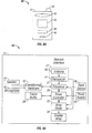
- FIG. 2 is a system block diagram illustrating one embodiment of an electronic device that may incorporate aspects of the invention.
- the electronic device includes a processor 21 which may be any general purpose single- or multi-chip microprocessor such as an ARM, Pentium ® , Pentium II ® , Pentium III ® , Pentium IV ® , Pentium ® Pro, an 8051, a MIPS ® , a Power PC ® , an ALPHA ® , or any special purpose microprocessor such as a digital signal processor, microcontroller, or a programmable gate array.
- the processor 21 may be configured to execute one or more software modules.
- the processor may be configured to execute one or more software applications, including a web browser, a telephone application, an email program, or any other software application.
- the processor 21 is also configured to communicate with an array driver 22.
- the array driver 22 includes a row driver circuit 24 and a column driver circuit 26 that provide signals to a display array or panel 30.
- the cross section of the array illustrated in Figure 1 is shown by the lines 1-1 in Figure 2 .
- the row/column actuation protocol may take advantage of a hysteresis property of these devices illustrated in Figure 3 . It may require, for example, a 10 volt potential difference to cause a movable layer to deform from the relaxed state to the actuated state. However, when the voltage is reduced from that value, the movable layer maintains its state as the voltage drops back below 10 volts.
- the movable layer does not relax completely until the voltage drops below 2 volts.
- a window of applied voltage about 3 to 7 V in the example illustrated in Figure 3 , within which the device is stable in either the relaxed or actuated state. This is referred to herein as the "hysteresis window” or "stability window.”
- the row/column actuation protocol can be designed such that during row strobing, pixels in the strobed row that are to be actuated are exposed to a voltage difference of about 10 volts, and pixels that are to be relaxed are exposed to a voltage difference of close to zero volts.
- each pixel sees a potential difference within the "stability window" of 3-7 volts in this example.
- This feature makes the pixel design illustrated in Figure 1 stable under the same applied voltage conditions in either an actuated or relaxed pre-existing state. Since each pixel of the interferometric modulator, whether in the actuated or relaxed state, is essentially a capacitor formed by the fixed and moving reflective layers, this stable state can be held at a voltage within the hysteresis window with almost no power dissipation. Essentially no current flows into the pixel if the applied potential is fixed.
- a display frame may be created by asserting the set of column electrodes in accordance with the desired set of actuated pixels in the first row.
- a row pulse is then applied to the row 1 electrode, actuating the pixels corresponding to the asserted column lines.
- the asserted set of column electrodes is then changed to correspond to the desired set of actuated pixels in the second row.
- a pulse is then applied to the row 2 electrode, actuating the appropriate pixels in row 2 in accordance with the asserted column electrodes.
- the row 1 pixels are unaffected by the row 2 pulse, and remain in the state they were set to during the row 1 pulse. This may be repeated for the entire series of rows in a sequential fashion to produce the frame.
- the frames are refreshed and/or updated with new display data by continually repeating this process at some desired number of frames per second.
- protocols for driving row and column electrodes of pixel arrays to produce display frames are also well known and may be used in conjunction with the present invention.
- Figures 4 , 5A, and 5B illustrate one possible actuation protocol for creating a display frame on the 3x3 array of Figure 2 .
- Figure 4 illustrates a possible set of column and row voltage levels that may be used for pixels exhibiting the hysteresis curves of Figure 3 .
- actuating a pixel involves setting the appropriate column to -V bias , and the appropriate row to + ⁇ V, which may correspond to - 5 volts and +5 volts, respectively Relaxing the pixel is accomplished by setting the appropriate column to +V bias , and the appropriate row to the same + ⁇ V, producing a zero volt potential difference across the pixel.
- the pixels are stable in whatever state they were originally in, regardless of whether the column is at +V bias , or -V bias .
- voltages of opposite polarity than those described above can be used, e.g., actuating a pixel can involve setting the appropriate column to +V bias , and the appropriate row to - ⁇ V.
- releasing the pixel is accomplished by setting the appropriate column to -V bias , and the appropriate row to the same - ⁇ V, producing a zero volt potential difference across the pixel.
- Figure 5B is a timing diagram showing a series of row and column signals applied to the 3x3 array of Figure 2 which will result in the display arrangement illustrated in Figure 5A , where actuated pixels are non-reflective.
- the pixels Prior to writing the frame illustrated in Figure 5A , the pixels can be in any state, and in this example, all the rows are at 0 volts, and all the columns are at +5 volts. With these applied voltages, all pixels are stable in their existing actuated or relaxed states.
- pixels (1,1), (1,2), (2,2), (3,2) and (3,3) are actuated.
- columns 1 and 2 are set to -5 volts, and column 3 is set to +5 volts. This does not change the state of any pixels, because all the pixels remain in the 3-7 volt stability window.
- Row 1 is then strobed with a pulse that goes from 0, up to 5 volts, and back to zero. This actuates the (1,1) and (1,2) pixels and relaxes the (1,3) pixel. No other pixels in the array are affected.
- column 2 is set to -5 volts, and columns 1 and 3 are set to +5 volts.
- Row 3 is similarly set by setting columns 2 and 3 to -5 volts, and column 1 to +5 volts.
- the row 3 strobe sets the row 3 pixels as shown in Figure 5A . After writing the frame, the row potentials are zero, and the column potentials can remain at either +5 or -5 volts, and the display is then stable in the arrangement of Figure 5A . It will be appreciated that the same procedure can be employed for arrays of dozens or hundreds of rows and columns.
- FIGS 6A and 6B are system block diagrams illustrating an embodiment of a display device 40.
- the display device 40 can be, for example, a cellular or mobile telephone.
- the same components of display device 40 or slight variations thereof are also illustrative of various types of display devices such as televisions and portable media players.
- the display device 40 includes a housing 41, a display 30, an antenna 43, a speaker 45, an input device 48, and a microphone 46.
- the housing 41 is generally formed from any of a variety of manufacturing processes as are well known to those of skill in the art, including injection molding and vacuum forming.
- the housing 41 may be made from any of a variety of materials, including, but not limited to, plastic, metal, glass, rubber, and ceramic, or a combination thereof.
- the housing 41 includes removable portions (not shown) that may be interchanged with other removable portions of different color, or containing different logos, pictures, or symbols.
- the display 30 of exemplary display device 40 may be any of a variety of displays, including a bi-stable display, as described herein.
- the display 30 includes a flat-panel display, such as plasma, EL, OLED, STN LCD, or TFT LCD as described above, or a non-flat-panel display, such as a CRT or other tube device, as is well known to those of skill in the art.
- the display 30 includes an interferometric modulator display, as described herein.
- the components of one embodiment of exemplary display device 40 are schematically illustrated in Figure 6B .
- the illustrated exemplary display device 40 includes a housing 41 and can include additional components at least partially enclosed therein.
- the exemplary display device 40 includes a network interface 27 that includes an antenna 43, which is coupled to a transceiver 47.
- the transceiver 47 is connected to a processor 21, which is connected to conditioning hardware 52.
- the conditioning hardware 52 may be configured to condition a signal (e.g., filter a signal).
- the conditioning hardware 52 is connected to a speaker 45 and a microphone 46.
- the processor 21 is also connected to an input device 48 and a driver controller 29.
- the driver controller 29 is coupled to a frame buffer 28 and to an array driver 22, which in turn is coupled to a display array 30.
- a power supply 50 provides power to all components as required by the particular exemplary display device 40 design.
- the network interface 27 includes the antenna 43 and the transceiver 47 so that the exemplary display device 40 can communicate with one or more devices over a network. In one embodiment, the network interface 27 may also have some processing capabilities to relieve requirements of the processor 21.
- the antenna 43 is any antenna known to those of skill in the art for transmitting and receiving signals. In one embodiment, the antenna transmits and receives RF signals according to the IEEE 802.11 standard, including IEEE 802.11(a), (b), or (g). In another embodiment, the antenna transmits and receives RF signals according to the BLUETOOTH standard. In the case of a cellular telephone, the antenna is designed to receive CDMA, GSM, AMPS, or other known signals that are used to communicate within a wireless cell phone network.
- the transceiver 47 pre-processes the signals received from the antenna 43 so that they may be received by and further manipulated by the processor 21.
- the transceiver 47 also processes signals received from the processor 21 so that they may be transmitted from the exemplary display device 40 via the antenna 43.
- the transceiver 47 can be replaced by a receiver.
- network interface 27 can be replaced by an image source, which can store or generate image data to be sent to the processor 21.
- the image source can be a digital video disc (DVD) or a hard-disc drive that contains image data, or a software module that generates image data.
- Processor 21 generally controls the overall operation of the exemplary display device 40.
- the processor 21 receives data, such as compressed image data from the network interface 27 or an image source, and processes the data into raw image data or into a format that is readily processed into raw image data.
- the processor 21 then sends the processed data to the driver controller 29 or to frame buffer 28 for storage.
- Raw data typically refers to the information that identifies the image characteristics at each location within an image. For example, such image characteristics can include color, saturation, and gray-scale level.
- the processor 21 includes a microcontroller, CPU, or logic unit to control operation of the exemplary display device 40.
- Conditioning hardware 52 generally includes amplifiers and filters for transmitting signals to the speaker 45, and for receiving signals from the microphone 46. Conditioning hardware 52 may be discrete components within the exemplary display device 40, or may be incorporated within the processor 21 or other components.
- the driver controller 29 takes the raw image data generated by the processor 21 either directly from the processor 21 or from the frame buffer 28 and reformats the raw image data appropriately for high speed transmission to the array driver 22. Specifically, the driver controller 29 reformats the raw image data into a data flow having a raster-like format, such that it has a time order suitable for scanning across the display array 30. Then the driver controller 29 sends the formatted information to the array driver 22.
- a driver controller 29, such as a LCD controller is often associated with the system processor 21 as a stand-alone Integrated Circuit (IC), such controllers may be implemented in many ways. They may be embedded in the processor 21 as hardware, embedded in the processor 21 as software, or fully integrated in hardware with the array driver 22.
- IC Integrated Circuit
- the array driver 22 receives the formatted information from the driver controller 29 and reformats the video data into a parallel set of waveforms that are applied many times per second to the hundreds and sometimes thousands of leads coming from the display's x-y matrix of pixels.
- driver controller 29 is a conventional display controller or a bi-stable display controller (e.g., an interferometric modulator controller).
- array driver 22 is a conventional driver or a bi-stable display driver (e.g., an interferometric modulator display).
- a driver controller 29 is integrated with the array driver 22.
- display array 30 is a typical display array or a bi-stable display array (e.g., a display including an array of interferometric modulators).
- the input device 48 allows a user to control the operation of the exemplary display device 40.
- input device 48 includes a keypad, such as a QWERTY keyboard or a telephone keypad, a button, a switch, a touch-sensitive screen, or a pressure- or heat-sensitive membrane.
- the microphone 46 is an input device for the exemplary display device 40. When the microphone 46 is used to input data to the device, voice commands may be provided by a user for controlling operations of the exemplary display device 40.
- Power supply 50 can include a variety of energy storage devices as are well known in the art.
- power supply 50 is a rechargeable battery, such as a nickel-cadmium battery or a lithium ion battery.
- power supply 50 is a renewable energy source, a capacitor, or a solar cell including a plastic solar cell, and solar-cell paint.
- power supply 50 is configured to receive power from a wall outlet.
- control programmability resides, as described above, in a driver controller which can be located in several places in the electronic display system. In some embodiments, control programmability resides in the array driver 22. Those of skill in the art will recognize that the above-described optimizations may be implemented in any number of hardware and/or software components and in various configurations.
- Figures 7A-7E illustrate five different embodiments of the movable reflective layer 14 and its supporting structures.
- Figure 7A is a cross section of the embodiment of Figure 1 , where a strip of metal material 14 is deposited on orthogonally extending supports 18.
- the moveable reflective layer 14 is attached to supports at the corners only, on tethers 32.
- the moveable reflective layer 14 is suspended from a deformable layer 34, which may comprise a flexible metal.
- the deformable layer 34 connects, directly or indirectly, to the substrate 20 around the perimeter of the deformable layer 34. These connections are herein referred to as support posts.
- the embodiment illustrated in Figure 7D has support post plugs 42 upon which the deformable layer 34 rests.
- the movable reflective layer 14 remains suspended over the gap, as in Figures 7A-7C , but the deformable layer 34 does not form the support posts by filling holes between the deformable layer 34 and the optical stack 16. Rather, the support posts are formed of a planarization material, which is used to form support post plugs 42.
- the embodiment illustrated in Figure 7E is based on the embodiment shown in Figure 7D , but may also be adapted to work with any of the embodiments illustrated in Figures 7A-7C , as well as additional embodiments not shown. In the embodiment shown in Figure 7E , an extra layer of metal or other conductive material has been used to form a bus structure 44. This allows signal routing along the back of the interferometric modulators, eliminating a number of electrodes that may otherwise have had to be formed on the substrate 20.
- the interferometric modulators function as direct-view devices, in which images are viewed from the front side of the transparent substrate 20, the side opposite to that upon which the modulator is arranged.
- the reflective layer 14 optically shields the portions of the interferometric modulator on the side of the reflective layer opposite the substrate 20, including the deformable layer 34. This allows the shielded areas to be configured and operated upon without negatively affecting the image quality.
- Such shielding allows the bus structure 44 in Figure 7E , which provides the ability to separate the optical properties of the modulator from the electromechanical properties of the modulator, such as addressing and the movements that result from that addressing.
- This separable modulator architecture allows the structural design and materials used for the electromechanical aspects and the optical aspects of the modulator to be selected and to function independently of each other.
- the embodiments shown in Figures 7C-7E have additional benefits deriving from the decoupling of the optical properties of the reflective layer 14 from its mechanical properties, which are carried out by the deformable layer 34. This allows the structural design and materials used for the reflective layer 14 to be optimized with respect to the optical properties, and the structural design and materials used for the deformable layer 34 to be optimized with respect to desired mechanical properties.
- An internal source of illumination may be provided for illumination of reflective display devices in dark ambient environments.
- integration of an illumination source in display devices comprising a plurality of display elements includes laminating a film or film stack providing some or all of the optical functions to a substrate. Light can be injected into this film or film stack and can propagate therein across the face of the display device.
- a light guide film or film stack may be laminated to a substrate using a light-diffusive pressure-sensitive adhesive (PSA).
- PSA light-diffusive pressure-sensitive adhesive
- the optical propagation region comprises a light guide film or film stack and does not include the substrate. In other embodiments, the optical propagation region comprises a light guide film or film stack and a substrate. Regardless of the particular configuration, the optical propagation region includes upper and lower interfaces that reflect light incident thereon at grazing incidence to support the propagation of light along the length of the light guide.
- the light guide includes a "turning film” (e.g., "prismatic film”) that forms the upper interface distal to the display elements that is configured to reflect (or "turn") rays propagating in the light guide towards the display elements.
- an optical isolation layer is introduced between the optical propagation region and the display elements in order to increase the reflectivity of the light at grazing incidence.
- the upper and lower interfaces separate the light guide from two materials which have refractive indices smaller than the smallest refractive index of the elements comprising the optical propagation region.
- grazing incidence is defined for rays propagating inside the optical propagation region at an angle that is larger than the largest of the two angles describing total internal reflection ("TIR") at each of the two interfaces, so that at grazing incidence the propagating rays experience total internal reflection at both the upper and lower interfaces of the optical propagation region.
- TIR total internal reflection
- the optical isolation layer is configured to reflect more than about 20%, about 25%, about 30%, about 35%, about 40%, about 45%, about 50%, about 55%, about 60%, about 65%, about 70%, about 75%, about 80%, about 85%, about 90%, about 95%, or higher of light incident on the optical isolation layer from within the optical propagation region at angles of incidence greater than about 40°, about 50°, about 55°, about 60°, about 65°, about 70°, about 75°, about 80°, about 85°, or higher relative to the normal to the lower interface of the optical propagation region.
- a "high" is configured to reflect more than about 20%, about 25%, about 30%, about 35%, about 40%, about 45%, about 50%, about 55%, about 60%, about 65%, about 70%, about 75%, about 80%, about 85%, about 90%, about 95%, or higher of light incident on the optical isolation layer from within the optical propagation region at angles of incidence greater than about 40°, about 50°, about 55°, about 60°, about 65°, about
- angle of incidence is, in some embodiments, at or above the largest TIR angle corresponding to the two interfaces (e.g., about 68° if the two TIR angles are about 39° and 68°) whereupon reflection of the incident light approaches 100%.
- Light at "lower" angles is partly reflected and partly refracted when it interacts with one of the interfaces of the optical propagation region where the angle of incidence is smaller than the total internal reflection angle of said interface.
- Other combinations of reflectivity of the optical isolation layer and angles of incidence are also possible.
- the optical isolation layer in addition to providing relatively high reflectivity for light rays at grazing incidence, is adapted to provide high transmittance of light rays at low angles of incidence (e.g., at the upper and/or lower interfaces).
- light for example redirected by a turning film or originating from the ambient, can pass freely through the optical isolation layer and into the display elements with reduced reflection from the surfaces of the optical isolation layer.
- light from the display elements e.g., reflected by interferometric modulators
- Interferometric modulators are generally specular in nature, so certain embodiments of display devices comprising interferometric modulators preferably comprise a light diffusive element (or "diffuser").
- a diffuser or other optical loss structure is adjacent to an optical light guide, light propagating through the light guide at grazing incidence, e.g., at angles greater than 40° (the "light guided modes"), which should be reflected within the light guide by total internal reflection, may instead be scattered one or multiple times and redirected into non-light guided modes, or absorbed due to the intrinsic material absorption of certain elements inside the optical system with which light may interact.
- Figure 8A schematically illustrates a cross-sectional portion of a display device 80 comprising an array of display elements 81 (e.g., interferometric modulators), a substrate 82 (e.g., comprising glass, plastic, etc.), an optical loss layer or structure 83 (e.g., comprising a diffuser, an absorber, a polarizer, a color filter, etc.), and a light guide 84. Because the light guide 84 is immediately adjacent to the optical loss layer 83, the reflectivity of light rays at grazing incidence on a lower interface of the optical propagation region between the light guide 84 and the optical loss layer 83 can be disadvantageously reduced.
- display elements 81 e.g., interferometric modulators
- a substrate 82 e.g., comprising glass, plastic, etc.
- an optical loss layer or structure 83 e.g., comprising a diffuser, an absorber, a polarizer, a color filter, etc.
- an example of the undesired effects that may be caused by adjacent optical loss layers 83 is that the light propagating in the light guide 84 may interact with an optical loss layer 83 having scattering properties, which may reduce the total amount of useful light carried by the light guide. Additionally, rays may be scattered at angles that are absorbed more strongly by certain components of the display device 80 (e.g., the display elements 81), which can reduce the illumination, brightness uniformity, color, and/or contrast of the display device 80.
- portions of the light scattered into the interferometric cavities may be absorbed regardless of the state of the interferometric modulators, which can result in a loss of light that reduces the brightness, uniformity, color, and/or contrast of the display device 80.
- the presence of an optical loss layer 83 directly adjacent to the light guide 84 can thereby cause unwanted scattering, which can disrupt the light propagation, or cause unwanted absorption, which can reduce uniformity and/or brightness.
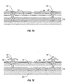
- FIG. 8B illustrates a portion of a display device 86 in which the optical loss layer 83 is separated from the light guide 84 by an air gap 85.
- the index of refraction of air is 1.0, which is less than the index of refraction of the light guide 84.
- an air gap 85 can increase the thickness of the display device 86 (e.g., by several hundred microns ( ⁇ m)) and can reduce the contrast of the display device 86. Forming the air gap 85 may involve increased complexity. Additionally, one or more anti-reflective coatings on one or more sides of the air gap 85 may be required (e.g., to achieve a certain contrast level), thereby significantly increasing the costs of manufacturing.
- an optical isolation layer (or "optical isolation region") comprising a film or a material is introduced between the optical propagation region and the optical loss layer (e.g., the diffuser) in order to increase the reflectivity of the light rays at grazing incidence.
- the index of refraction of the material of the optical isolation layer is different (e.g., lower) than the index of refraction of the optical propagation region
- an interface between the optical propagation region and the optical loss layer total internally reflects light incident thereon at grazing angles (e.g., angles greater than the critical angle).
- the optical propagation region comprises a planar or substantially flat light guide and the optical isolation layer is immediately adjacent to the light guide.
- the optical isolation layer is adapted to reflect more than about 20%, about 25%, about 30%, about 35%, about 40%, about 45%, about 50%, about 55%, about 60%, about 65%, about 70%, about 75 %, about 80%, about 85%, about 90%, about 95%, or higher of light incident on the optical isolation layer from within the optical propagation region at angles greater than about 40°, about 50°, about 55°, about 60°, about 65°, about 70°, about 75°, about 80°, about 85°, or higher relative to normal to the lower interface of the optical propagation region.
- the optical isolation layer is adapted to reflect more than about 40% of light incident on the lower interface at angles greater than about 70° relative to normal to the optical propagation region.
- the optical isolation layer is preferably between about 100 nanometers (nm) and 100 ⁇ m, more preferably between about 100 nm and 10 ⁇ m, or even more preferably between about 100 nm and 3 ⁇ m. Other thicknesses are also possible.
- the optical isolation layer in addition to providing relatively high reflectivity for light rays at grazing incidence, is adapted to provide high transmittance of light rays at low angles of incidence at the lower interface.
- the interface between the optical propagation region and the optical loss layer is essentially transparent for light incident thereon at lower angles (e.g., angles close to normal to the interface, such as turned towards the interface by a turning film or from the ambient) and has reduce Fresnel reflection.
- light for example redirected by a turning film at the upper interface or from the ambient propagating through the upper interface
- light for example redirected by a turning film at the upper interface or from the ambient propagating through the upper interface
- light for example redirected by a turning film on an upper interface or from the ambient propagating through the upper interface
- light from the display elements e.g., reflected by interferometric modulators
- decoupling an optical loss layer e.g., a diffusing layer or absorbing layer
- an optical loss layer e.g., a diffusing layer or absorbing layer
- an air gap e.g., using instead an optical isolation layer
- decoupling an optical loss layer from an optical propagation region without utilizing an air gap can advantageously increase the amount of light that propagates through the optical propagation region without substantially increasing thickness or significantly increasing the costs of manufacturing.
- such embodiments allow the efficient integration of a diffuser with a light guide, thereby enabling development of a light guide that performs independently of the state of the underlying display elements and/or optics.
- Other examples of optical parameters that can be changed without affecting the performance of the light guide include, for example, optical buffering the interferometric modulator, differences in the reflectivity of the interferometric modulator of different architectures, varying display content and brightness level, etc.
- the light guide can be treated as a "drop-in" module because the optical functionality of the light guide is decoupled from the state of the array of display elements onto which it is laminated or added.
- an illumination apparatus comprising an optical propagation region decoupled from an optical loss region (e.g., including polarizers, diffusers, color filters, absorbers, and the like) may be applied to a wide variety of display technologies (e.g., reflective liquid crystal, transmissive liquid crystal, transflective liquid crystal, electrophoretic, etc.).
- an optical propagation region decoupled from an optical loss region e.g., including polarizers, diffusers, color filters, absorbers, and the like
- display technologies e.g., reflective liquid crystal, transmissive liquid crystal, transflective liquid crystal, electrophoretic, etc.
- a diffuser When not optically decoupled from the optical propagation region, a diffuser can be responsible for a loss of optical energy in the optical propagation region (e.g., greater than about 25%, greater than about 50%, greater than about 75%, etc. depending on the length of the display device, the thickness of the diffuser, the thickness of the optical propagation region, and light diffusion strength (i.e., Haze level).
- a loss of optical energy in the optical propagation region e.g., greater than about 25%, greater than about 50%, greater than about 75%, etc. depending on the length of the display device, the thickness of the diffuser, the thickness of the optical propagation region, and light diffusion strength (i.e., Haze level).
- optically decoupling an optical propagation region from an optical loss layer is even higher because the combined optical losses of the light guided modes to both the optical loss layer (e.g., diffuser, absorbing layer) as well as the display elements (e.g., interferometric modulators) can be very severe, and decoupling the optical propagation region (e.g., light guide film or film stack, light guide plus substrate, etc.) from the optical isolation layer implicitly decouples the optical propagation region from the display elements, as well.
- the optical propagation region e.g., light guide film or film stack, light guide plus substrate, etc.
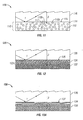
- Figure 9A illustrates a portion of a display device 90 comprising an array of display elements 91 (e.g., interferometric modulators), a substrate 92 (e.g., comprising glass, plastic, etc.), and an illumination apparatus comprising an optical loss layer 93 (e.g., comprising a diffuser, an absorber, a polarizer, a color filter, etc.), and an optical propagation region 97 comprising a light guide 94.
- the substrate 92 provides a means for supporting the display elements 91 and/or certain other layers during fabrication of the display elements 91.
- the illumination apparatus of the display device 90 further comprises an optical isolation layer 95 between the optical propagation region 97 and the optical loss layer 93.
- the optical isolation layer 95 comprises a material.
- the material is a solid. In some embodiments, the material is a liquid (e.g., a viscous liquid). In some embodiments, the material is gel-like.
- the optical isolation layer 95 is configured such that light propagating through the optical propagation region 97 at grazing incidence does not interact with the optical loss layer 93, but also such that light propagating through the optical propagation region 97 at low angles (e.g., due to being turned towards the array of display elements 91 by a turning film of the light guide 94 or from the ambient) may interact with the optical loss layer 93, the substrate 92, and the array of display elements 91,
- Integrating the optical isolation layer 95 within the display device 90 allows it to be formed before, during, and/or after manufacture of the display elements 91 on the substrate 92.
- the optical loss layer 93 may be deposited onto the substrate 92 as a first step of the manufacturing.
- the substrate 92 can act as a means for supporting the display elements 91 and/or certain other layers during fabrication in such embodiments. Coating processes including spin coating, blade coating, spray coating, fluid dispensing, film coating, etc. may be employed.
- Deposition may be by suitable deposition techniques, including, but not limited to, chemical vapor deposition (CVD) and/or physical vapor deposition (PVD).
- the optical loss layer 93 may also be laminated to the substrate 92 in certain embodiments.
- the optical isolation layer 95 is applied onto the light guide 94, and then the stack including the optical isolation layer 95 and the light guide 94 is applied onto the substrate 92.
- Pressure sensitive adhesive may be used.
- the optical loss layer 93 comprises a diffuser
- the diffuser comprises an adhesive matrix with scatter particles incorporated therein.
- the optical isolation layer 95 may be formed on the optical loss layer 93.
- the optical isolation layer 95 may be deposited or applied onto the optical loss layer 93 on the substrate 92.
- the substrate 92 can act as a means for supporting the display elements 91 and/or certain other layers during fabrication in such embodiments.
- each layer may be sequentially deposited.
- the optical isolation layer 95 may also be integrated with the optical loss layer 93, for example in the structure 98 of Figure 9A and the structure 118 described below with respect to Figure 11 .
- the integrated structure 98 comprising the optical isolation layer 95 and the optical loss layer 93 may be deposited onto the opposite side of the substrate 92 as the display elements 91.
- the substrate 92 can act as a means for supporting the display elements 91 and/or certain other layers during fabrication in such embodiments.
- the integrated structure 98 is applied onto the light guide 94, and then the stack including the integrated structure 98 and the light guide 94 is applied onto the substrate 92 or onto a display device comprising the substrate 92 and display elements 91.
- the integrated structure 98 has dual optical functionality: optical isolation and optical loss.
- the integrated structure 98 comprises a multi-functional pressure sensitive adhesive which attaches the light guide 94 to the side of the substrate 92 that is opposite from the display elements side 91.
- the optical isolation layer 95 After formation of the optical isolation layer 95, ordinary deposition and patterning steps used to form display elements (e.g., interferometric modulators, as described above) may be performed to fabricate the display elements 91 on the other side of the substrate 92, which can be used for structural support of the display elements 91 and/or certain other layers during fabrication.
- the light guide 94 may be attached (e.g., laminated, embossed, applied, etc.) to the opposite side of the substrate 92 on the optical isolation layer 95.
- the light guide 94 including a turning film may be laminated onto the substrate 92.
- the light guide 94 may be attached by first laminating a base film (or layer or multi-layer stack) to the substrate 92 and subsequently laminating a prismatic film to the base film.
- the light guide 94 may be attached by first laminating a prismatic film onto a base film (or layer or multi-layer stack) and subsequently laminating the base film with the prismatic film thereon onto the substrate 92.
- a different order of steps may be used.
- the display elements 91 e.g., interferometric modulators
- the display elements 91 can be formed prior to either or both the optical loss layer 93 and the optical isolation layer 95. Other variations are also possible.
- Figure 9B illustrates a portion of a display device 96 comprising an array of display elements 91 (e.g., interferometric modulators), and an illumination apparatus comprising a substrate 92 (e.g., comprising glass, plastic, etc.), an optical loss layer 93, and a light guide 94.
- the optical propagation region 97 comprises the light guide film or film stack 94 and the substrate 92.
- the substrate 92 provides a means for supporting the display elements 91 and/or certain other layers during fabrication of the display elements 91.
- the optical loss layer 93 is adjacent to the array of display elements 91, so the optical isolation layer 95 is between the substrate 92 and the optical loss layer 93.
- the embodiment illustrated in Figure 9B also comprises an optical propagation region 97 decoupled from an optical loss layer 93 and consequently also decoupled from the display elements 91.
- an illumination apparatus comprising a substrate 92 (e.g., comprising glass, plastic, etc.), an optical loss layer 93, and a light guide 94.
- a substrate 92 e.g., comprising glass, plastic, etc.
- an optical loss layer 93 e.g., comprising glass, plastic, etc.
- a light guide 94 e.g., a light guide
- the substrate 92 is configured such that light propagating through the optical light guide 94 at grazing incidence does not interact with the optical loss layer 93, but also such that light propagating through the light guide 94 at low angles may be transmitted through with the optical loss layer 93, the substrate 92, and be incident on the array of display elements 91.
- the substrate 92 comprises a material having an index of refraction that is lower than the index of refraction of the light guide 94.
- the substrate 92 may comprise quartz (having an index of refraction of about 1.45), aluminosilicate display glass (having an index of refraction of about 1.52), etc.
- the separate optical isolation layer 95 discussed above may be eliminated and the substrate may be used as the optical isolation layer, advantageously reducing costs.
- embodiments including a separate optical isolation layer 95 may provide more flexibility in selection of materials.
- the optical isolation layer 95 is formed on the light guide 94 so that the entire stack above the substrate 92 can be applied in one step to produce the display device 96.
- the optical isolation layer 95 is deposited onto the substrate 92 before the light guide 94 is applied onto the substrate 92. It will be appreciated that the substrate 92 can act as a means for supporting the display elements 91 and/or certain other layers during fabrication in such embodiments.
- each layer may be sequentially deposited.
- the optical loss layer 93 may be disposed on the optical isolation layer 95 using deposition or lamination techniques, for example, as described above.
- ordinary deposition and patterning steps used to form display elements e.g., interferometric modulators, as described above
- the light guide 94 may be attached (e.g., laminated, embossed, applied, etc.) on the opposite side of the substrate 92 either before, after, or during manufacturing the display elements 91.
- the light guide 94 including a turning film may be laminated onto the substrate 92.
- the light guide 94 may be attached by first laminating a base film (or layer or multi-layer stack) to the substrate 92 and subsequently laminating a prismatic film to the base film.
- the light guide 94 may be attached by first laminating a prismatic film onto a base film (or layer or multi-layer stack) and subsequently laminating the base film with the prismatic film thereon onto the substrate 92.
- the light guide 94 and the substrate 92 form the optical propagation region 97.
- the optical loss layer and/or the optical isolation layer are formed after forming the display elements (e.g., interferometric modulators).
- the optical isolation layer 95 may be integrated with the optical loss layer 93, for example in the structure 98 of Figures 9A and 9B and the structure 118 described below with respect to Figure 11 .
- the optical isolation layer integrated with the optical loss layer 98 may be deposited onto the same side of the substrate 92 as the display elements 91. It will be appreciated that the substrate 92 can act as a means for supporting the display elements 91 and/or certain other layers during fabrication in such embodiments.
- Figure 10A illustrates a portion of an example embodiment of an illumination apparatus 100 comprising an optical isolation layer 104 between an optical propagation region 106 and an optical loss layer 102.
- the optical loss layer 102 may comprise a diffuser, color filter, absorber, polarizer, or other type of layer.
- the optical isolation layer 104 comprises a material.
- the material is a solid.
- the material is a liquid (e.g., a viscous liquid).
- the material is gel-like.
- the optical isolation layer 104 comprises a substrate.
- the optical propagation region 106 may comprise, for example, a light guide (e.g., as illustrated in Figure 9A ), a light guide and a substrate (e.g., as illustrated in Figure 9B ), a light guide with a turning film laminated thereon, adhesive layers, and the like.
- the light guide film may comprise a material such as polycarbonate, glass (e.g., aluminosilicate, borosilicate, etc.), and the like.
- Polycarbonate has an index of refraction of about 1.59 at wavelengths in the visible spectrum
- glass typically has an index of refraction of about 1.52 at visible wavelengths.
- the optical isolation layer 104 has an index of refraction that is lower than the index of refraction of the optical propagation region 106.
- the difference in indices of refraction between the optical propagation region 106 and the optical isolation layer 104 causes light rays at grazing incidence to be totally internally reflected from the lower interface 105 between the optical propagation region 106 and the optical isolation layer 104.
- the optical isolation layer 104 may have an index of refraction lower than about 1.59, and when the optical propagation region 106 comprises glass, the optical isolation layer 104 may have an index of refraction lower than about 1.52.
- the optical isolation layer 104 may, for example, comprise silicones (e.g., optically clear silicone-based adhesives) having indices of refraction between 1.4 and 1.45, nanoporous glassy materials (e.g., nanoporous silica, spin-on glasses, etc.) having indices of refraction between 1.4 and 1.45, fluoropolymers (e.g., amorphous transparent fluoropolymers such as DuPont NC-211) having good adhesion to glass and plastics and indices of refraction between about 1.3 and 1.4, and others (e.g., aerogels having indices of refraction less than about 1.2 and acrylate-based materials having indices of refraction of about 1.47).
- silicones e.g., optically clear silicone-based adhesives
- nanoporous glassy materials e.g., nanoporous silica, spin-on glasses, etc.
- fluoropolymers e.g., amorph
- Acrylate-based materials are preferred for low costs and ease of integration, but materials with an index of refraction that is substantially less than the index of refraction of the optical propagation region 106 (e.g., having an index of refraction difference of about 0.1 or more) are preferred for optical characteristics, as described below with respect to Figure 10C . Other materials can also be used.
- Light propagating through the material of the optical isolation layer 104 at low angles of incidence preferably loses less than about 4% of its intensity or flux, more preferably loses less than about 2% of its intensity or flux, even more preferably loses less than about 1% of its intensity or flux, still more preferably loses less than about 0.6% of its intensity or flux, yet still more preferably loses less than about 0.2% of its intensity or flux, or yet even still more preferably loses less than about 0.1 % of its intensity or flux.
- This loss may be due, for example, to Fresnel reflection as a result of the mismatch in index of refraction.
- a polycarbonate optical propagation region 106 (having an index of refraction of about 1.59) coupled to an acrylate-based optical isolation layer 104 (having an index of refraction of about 1.47) has a polarization-averaged reflectivity of about 0.2%
- a polycarbonate optical propagation region 106 coupled to a fluoropolymer optical isolation layer 104 (having an index of refraction of about 1.37) has a polarization-averaged reflectivity of about 0.6%
- the material that comprises the optical isolation layer 106 may be modified.
- polymethyl methacrylate (PMMA) has an index of refraction of about 1.47, which, coupled to an aerogel optical isolation layer 104 has a polarization-averaged reflectivity of about 1%.
- PMMA optical propagation region 106 coupled to a fluoropolymer optical isolation layer 104 has a polarization-averaged reflectivity of about 0.1%.
- an illumination apparatus comprising an air gap 85 between the optical propagation region 84 and the optical loss layer 83 (e.g., as illustrated in Figure 8B )
- light propagating through the air gap 85 at low angles of incidence e.g., due to being turned by a light turning film of the optical propagation region 84 or from the ambient
- Figure 10B illustrates an angle of propagation, ⁇ i, (e.g., angle of incidence) propagating through an optical propagation region 106.
- the angle of incidence, ⁇ i is the angle from the normal to an interface 105 between the optical propagation region 106 and the optical isolation layer 104.
- Light at angles of grazing incidence are typically larger than about 40° from said normal to the interface.
- the material of the optical isolation layer 104 is selected at least in part by modeling with Fresnel equations, which describe the reflectivity between materials having different indices of refraction at different angles and light polarizations.
- Figure 10C depicts the average reflectivity for S and P polarizations of various substances in accordance with certain embodiments of the illumination apparatus 100 of Figure 10A , calculated for the interface with the smaller refractive index difference of the light guide (i.e., the interface 105 in embodiments in which the light guide 106 is adjacent to air at the interface comprising the turning features).
- Solid curve 107 depicts the average reflectivity of an optical propagation region 106 comprising polycarbonate having an index of refraction of about 1.59 and an optical isolation layer 104 comprising a fluoropolymer having an index of refraction of about 1.37. The difference in the indices of refraction is about 0.22 (1.59 - 1.37). The reflectivity for angles of incidence greater than about 58° is 100% and the reflectivity for angles of incidence below about 50° is nearly zero.
- Dotted curve 108 depicts the average reflectivity of an optical propagation region 106 comprising polycarbonate having an index of refraction of about 1.59 and an optical isolation layer 104 comprising silicone having an index of refraction of about 1.41.
- the difference in the indices of refraction is about 0.18 (1.59 - 1.41).
- the reflectivity for angles of incidence greater than about 62° is 100% and the reflectivity for angles of incidence below about 55° is nearly zero.
- Dashed curve 109 depicts the average reflectivity of an optical propagation region 106 comprising polycarbonate having an index of refraction of about 1.59 and an optical isolation layer 104 comprising an acrylate-based material having an index of refraction of about 1.47.
- the difference in the indices of refraction is about 0.12 (1.59 - 1.47).
- the reflectivity for angles of incidence greater than about 67° is 100% and the reflectivity for angles of incidence below about 60° is nearly zero.
- the other interface of the light guide assumed here to have a larger refractive index difference, exhibits a similar reflectivity behavior as function of incidence angle where total internal reflection starts at substantially smaller angles of incidence (e.g., 39° for polycarbonate-air) than the TIR angles shown in Figure 10C (e.g., about 60° or larger).
- Certain embodiments of the present invention increase (e.g., maximize) the range of angles which experience TIR at the upper and lower interfaces of the light guide 106 while minimizing the sum of the reflections at angles close to normal to the upper and lower interfaces.
- each of the curves 107, 108, 109 depicts the average reflectivity as asymptotically approaching about 0% at about 40°, it will be appreciated that the reflectivity may be affected by Fresnel reflection, as described above.
- the average reflectivity of the solid curve 107 at an angle of incidence of about 0° i.e., normal incidence to the interface 105
- the average reflectivity of the dotted curve 108 at an angle of incidence of about 0° is about 0.4%
- the average reflectivity of the dashed curve 109 at an angle of incidence of about 0° is about 0.2%.
- the average reflectivity at an angle of incidence of about 0° of a curve depicting the average reflectivity of an optical propagation region 84 comprising polycarbonate having an index of refraction of about 1.59 and an air gap 85 having an index of refraction of about 1.0 at an angle of incidence of about 0° is about 5.2%.
- the loss of intensity or flux in such an illumination apparatus at such angles is disadvantageously large in comparison to illumination apparatus comprising an optical isolation layer comprising, for example, material having a higher index than air and that more closely matches the index of the optical propagation region, in addition to the problems associated with increased thickness and manufacturing costs discussed above.
- Figure 11 is a cross section of a portion of another example embodiment of an illumination apparatus 110 comprising an optical propagation region 116 decoupled from an optical loss layer by an optical isolation layer comprising an engineered volume diffuser 118.
- the optical propagation region 116 may comprise, for example, a light guide (e.g., as illustrated in Figure 9A ), a light guide and a substrate (e.g., as illustrated in Figure 9B ), a light guide with a turning film laminated thereon, adhesive layers, and the like.
- the volume diffuser 118 is engineered so that light at grazing incidence in the light guide 116 (e.g., the ray 1 in Figure 11 ) is totally internal reflected and does not substantially.interact with the diffuser 118, while light at lower incidence angles in the light guide 116 (e.g., ray 2 in Figure 11 ) interacts with the diffuser 118 and is subsequently scattered.
- the engineered volume diffuser 118 can provide multiple optical functions: acting as an optical isolation layer for the light guide 116, reducing reflection for lower incidence light at the lower interface 115 of the light guide 116, and diffusing light turned by the light turning microstructure of the light guide 116 or originating from the ambient above the display 110.
- the engineered volume diffuser 118 comprises a base material (or "matrix") 114 and a filler (or "microstructure”) 112 disposed therein.
- the filler comprise particles or particulates or voids. These particulates or voids may have a size and/or geometry that scatters light. In some embodiments these particulates are absorbing. In various embodiments, for example, the particulates may absorb all of the visible spectrum and diffuse light. (In other embodiments, the particulates may absorb a portion of the visible spectrum and filter out color. In certain embodiments, the particulates are elongated and may be oriented similarly so as to polarize light.)
- the filler or microstructure 112 occupies about 10%, about 5%, or less by volume of the engineered volume diffuser 118.
- the base or matrix material 114 has an index of refraction lower than the index of refraction of the optical propagation region 116. Accordingly, the lower interface 115 between the optical propagation region 116 and the engineered volume diffuser 118 total internally reflects light incident thereon at grazing angles (e.g., angles greater than the critical angle relative to the interface 115 between the optical propagation region 116 and the matrix material 114 of the diffuser 118), while the interface 115 is essentially transparent for light incident thereon at higher angles (e.g., angles close to normal to the interface 115).
- the microstructurel 12 has an index of refraction that is higher and/or lower than the index of refraction of the base material 114.
- the feature 112a has an index of refraction lower than the index of refraction of the optical propagation region 116. Accordingly, the lower interface 115 between the optical propagation region 116 and the at least one microstructure 112a total internally reflects light incident thereon at grazing angles (e.g., angles greater than the critical angle), while the interface 115 is essentially transparent for light incident thereon at higher angles (e.g., angles close to normal to the interface 115).
- At least one microstructure 112a is not spaced from the interface 115, and the microstructure 112a does not have an index of refraction lower than the index of refraction of the optical propagation region 116. Accordingly, the light incident on the microstructure 112a at the lower interface at grazing angles (e.g., angles greater than the critical angle) may be affected. However, in embodiments in which a density of the features 112 is low such that there an area of microstructure 112a at the interface 115 is low with respect to the total area of the interface 115, such losses may be rendered insignificant (e.g., negligible).
- the volume diffuser 118 comprises an effective interface layer 117 (e.g., comprising material of the matrix 114) between the feature 112b and the interface 115.
- an effective interface layer 117 e.g., comprising material of the matrix 114
- the effective interface layer 117 becomes thicker, there is a reduced opportunity for interaction with the microstructures 112b. Accordingly, light incident on the interface 115 at grazing angles (e.g., angles greater than the critical angle) does not substantially interact with the microstructure 112b when the thickness of the layer 117 is sufficiently thick so that evanescent fields decay to negligible levels for the particular grazing angle.
- a thickness of the layer 117 is less than about 0.5 ⁇ m.
- a thickness of the layer 117 is less than about 1 ⁇ m. Other thicknesses are also possible and the thickness selected may in some embodiments depend on the indices of refraction of the optical propagation region 116 and the index of refraction of the matrix 114.
- the illumination apparatus 110 comprises an optical propagation region 116 including supplemental plastic films that are coated with a light diffusing coating and/or is fabricated on an interferometric modulator substrate glass.
- the optical propagation region 116 comprises a light guide (e.g., the optical propagation region 97 illustrated in Figure 9A ) and the optical isolation layer and optical loss layer are integrated in an engineered volume diffuser (e.g., the structure 98 illustrated in Figure 9A or the structure 118 illustrated in Figure 11 )
- the diffuser may comprise a light-diffusive pressure sensitive adhesive (PSA).
- PSA light-diffusive pressure sensitive adhesive
- the diffuser may comprise a particle-filled glass-like material (an "in-glass diffuser") on the same side of the substrate as the display elements.
- Glass-like materials include glasses obtained by heat treatment of organosilicon spin-on glasses, glasses obtained by heat treatment of sol-gel type materials, powdered glass dispersed in a binder, and others.
- the optical propagation region 116 comprises a light guide (e.g., the optical propagation region 97 illustrated in Figure 9A ) and the optical isolation layer and optical loss layer are integrated in an engineered volume diffuser (e.g., the structure 98 illustrated in Figure 9A or the structure 118 illustrated in Figure 11 )
- the diffuser may also comprise an in-glass diffuser on the opposite side of the substrate as the display elements.
- the illumination apparatus 110 comprises an optical propagation region 116 including interferometric modulator substrate glass and/or supplemental plastic films coated with a light diffusing formulation of an adhesive, such as a low-index PSA.
- Such embodiments may have reflectivity plots similar to those described above with respect to Figure 10C for the base material 114 versus the optical propagation region 116.
- the microstructures 112 may be any size or shape, and may be selected for certain properties of desired optical loss.
- the microstructures 112 may comprise light scattering features for embodiments in which the optical loss layer comprises an optical diffuser.
- the microstructures 112 may be configured to absorb light at certain wavelengths for embodiments in which the optical loss layer comprises a color filter.
- the microstructures 112 may be configured to absorb light at all visible wavelengths and a particular polarization for embodiments in which the optical loss layer comprises a diffuser or polarizer.
- the microstructures 112 are elongated (i.e., having a length greater than a width) and may be oriented along a preferred global direction for embodiments in which the optical loss layer comprises a polarizer.
- Figure 11 also illustrates an illumination apparatus 110 comprising an optical propagation region 116 and a layer 118.
- the optical propagation region 116 may comprise a light guide (e.g., as illustrated in Figure 9A ), a light guide and a substrate (e.g., as illustrated in Figure 9B ), a light guide with a turning film laminated thereon, adhesive layers, and the like.
- the turning features are configured to redirect light out of the optical propagation region 116 towards the interface 115.
- the layer 118 includes a matrix material 114 and microstructures 112 disposed in a matrix 114 with an index of refraction less than the smallest index of refraction of the layers comprising the optical propagation region 116.
- the layer 118 is configured to increase an amount of light that is totally internal reflected in the optical propagation region 116.
- the layer 118 may comprise a diffuser, for example where the microstructures are configured to scatter light.
- the layer 118 may comprise a color filter, for example where the microstructures are configured to absorb light at a selected wavelength.
- the layer 118 may comprise a polarizer, for example where the microstructures are elongated and/or are configured to absorb light at all visible wavelengths.
- the microstructures may have an index of refraction less than the index of refraction of the optical propagation region.
- the matrix may have an index of refraction less than the index of refraction of the optical propagation region.
- the optical isolation layer 118 of an illumination apparatus 110 comprises a volume hologram that changes the direction of light in either a controlled or uncontrolled manner.
- a hologram may comprise, for example, a holographic diffuser.
- This volume hologram may comprise matrix material having an index of refraction less than the index of refraction of the optical propagation region 116. Accordingly, light incident on the interface between the optical propagation region 116 and the hologram at oblique or grazing angles of incidence (greater than the critical angle) can be reflected by total internal reflection.
- light rays propagating through the light propagation region 116 at grazing incidence are contained via reflection within the optical propagation region 116, which has a higher refractive index than the engineered volume diffuser 118, while light originating in the ambient or turned by an illumination film at low angles of incidence are, for example, negligibly or minimally reflected.
- Figure 12 illustrates a portion of yet another example embodiment of an illumination apparatus 120 comprising an optical isolation layer 124 between an optical propagation region 126 and an optical loss layer 122 comprising a surface-structured optical element.
- the optical propagation region 126 may comprise, for example, a light guide (e.g., as illustrated in Figure 9A ), a light guide and a substrate (e.g., as illustrated in Figure 9B ), a light guide with a turning film laminated thereon, adhesive layers, and the like.
- the optical isolation layer 124 comprises a material having an index of refraction that is lower than the smallest index of refraction of the elements comprising the optical propagation region 126, thereby optically decoupling the optical propagation region 126 from the optical loss layer 122, e.g., via total internal reflection. Accordingly, the lower interface 125 between the optical propagation region 126 and the optical loss layer 122 total internally reflects light incident thereon at grazing angles (e.g., angles greater than the critical angle), while the interface 125 is essentially transparent for light incident thereon at lower angles (e.g., angles close to normal to the interface 125) so that light can interact with the optical element 122.
- the reflectivity plots of Figure 10C may also be applied to certain embodiments of the illumination apparatus illustrated in Figure 12 , as well.
- the optical loss layer 122 comprises a diffuser 122 including an engineered surface structure 123 having substantially spatially periodic, random, or spatially non-periodic features configured to diffuse light.
- a surface structure may comprise, for example, a holographic diffuser.
- the surface structure 123 of the diffuser 122 can be adjusted so that when the diffuser 122 is adjacent to the optical isolation layer 124 having a low index of refraction, the diffusion properties of the diffuser 122 are similar to when the diffusion properties of a diffuser 122 adjacent to air.
- the optical isolation layer 124 planarizes an interface 125 between the engineered surface structure 123 of the optical loss layer 122 and the rest of the illumination apparatus 120.
- Such a planar interface 125 may allow for better and/or easier attachment (e.g., lamination) of the optical loss layer 122 to the optical propagation region 126.
- attachment of the optical loss layer 122 to the optical propagation region 126 may otherwise include air gaps.
- the optical loss layer 122 may also comprise randomized holographic microstructured films (e.g., directional diffusers available from Physical Optics Corporation of Torrance, California, etc.), holographic gratings, and the like.
- the optical isolation layer 124 may be coupled to the optical loss layer 122 by, for example, wet coating the surface of the structured optical loss layer 122 in a roll-to-roll process so as to effectively planarize the surface relief 123.
- Figure 13A illustrates yet another example embodiment of an illumination apparatus 130 comprising an optical propagation region 136 decoupled from an optical loss layer 132 by an optical isolation layer 134 comprising low index material.
- the optical propagation region 136 may comprise, for example, a light guide (e.g., as illustrated in Figure 9A ), a light guide and a substrate (e.g., as illustrated in Figure 9B ), a light guide with a turning film laminated thereon, adhesive layers, and the like.
- the optical isolation layer 134 comprises a plurality of material layers in a multi-layer interference stack 134 that is configured to have a high reflectivity for light propagating through the optical propagation region 136 at grazing incidence and to have a low reflectivity for light at low angles of incidence (e.g., light turned by an illumination film or originating in the ambient).
- the plurality of material layers includes interference layers that utilize the properties of thin-film interference to obtain the desired reflection characteristics.
- the layers may include sub-wavelength (e.g., ⁇ /4) thin films of various materials (e.g., dielectric materials).
- the optical isolation layer 134 includes films having varying indices of refraction.
- films are provided that alternate between indices of refraction higher than the index of refraction of the optical propagation region 136 and lower than the index of refraction of the optical propagation region 136.
- the optical isolation layer 134 may include two films, one having an index of refraction higher than the index of refraction of the optical propagation region 136 and one having an index of refraction lower than the index of refraction of the optical propagation region 136.
- the multi-layer interference stack 134 can be used to decouple an optical propagation region 136 (e.g., a light guide film or film stack, a light guide film or film stack plus a substrate, etc.) from any variety of optical loss layer 132 (e.g., a diffuser, polarizer, colored filter, absorber, and the like). Accordingly, a lower. interface 137 between the optical propagation region 136 and the optical loss layer 132 total internally reflects light incident thereon at grazing angles (e.g., angles greater than the critical angle), while the interface 137 is essentially transparent for light incident thereon at higher angles (e.g., angles close to normal to the interface 137).
- optical loss layer 132 e.g., a diffuser, polarizer, colored filter, absorber, and the like.
- the optical isolation layer 134 can be physically provided (e.g., coated or deposited) on the optical propagation region 136, may be provided on a base film (or layer or multi-layer stack) that becomes part of the optical propagation region 136, or could be coated or deposited on the optical loss layer 132. Other methods of manufacturing are also possible.
- Figure 13B illustrates an example embodiment of a multi-layer interference stack 134 comprising a layer 131 of titanium dioxide (TiO 2 having an index of refraction of about 2.32, a layer 133 of magnesium fluoride (MgF 2 ) having an index of refraction of about 1.38, and a second layer 135 of titanium dioxide having an index of refraction of about 2.32.
- TiO 2 titanium dioxide
- MgF 2 magnesium fluoride
- At least one of the layers 131, 133, 135 comprises a material that has an index of refraction that is lower than the index of refraction of the optical propagation region 136, for example, magnesium fluoride in embodiments in which the optical propagation region 136 comprises glass having an index of refraction of about 1.52.
- Figure 13C graphically illustrates the photopic reflectivity of an example multi-layer interference stack 134 at different angles of incidence.
- Solid line 138 depicts the photopic reflectivity of an optical propagation region 136 comprising polycarbonate having an index of refraction of about 1.59 and a multi-layer interference stack 134 comprising 6.7 nm of titanium dioxide, 221.8 nm of magnesium fluoride, and 117.5 nm of titanium dioxide 131.
- the reflectivity for angles of incidence greater than about 70° is about 100% and the reflectivity of the angles of incidence below about 40° is nearly zero (e.g., due to Fresnel reflection, as described above).
- films, layers, components, and/or elements may be added, removed, or rearranged. Additionally, processing steps may be added, removed, or reordered.
- film and layer have been used herein, such terms as used herein may include film stacks and multilayers. Such film stacks and multilayers may be adhered to other structures using adhesives or may be formed on other structures using deposition or in other manners.
Abstract
Description
- This application claims priority benefit under 35 U.S.C. § 119(e) to
U.S. Provisional Application Serial No. 60/850,024, filed October 6, 2006 - Microelectromechanical systems (MEMS) include micro mechanical elements, actuators, and electronics. Micromechanical elements may be created using deposition, etching, and/or other micromachining processes that etch away parts of substrates and/or deposited material layers or that add layers to form electrical and electromechanical devices. One type of MEMS device is called an interferometric modulator. As used herein, the term interferometric modulator or interferometric light modulator refers to a device that selectively absorbs and/or reflects light using the principles of optical interference. In certain embodiments, an interferometric modulator may comprise a pair of conductive plates, one or both of which may be transparent and/or reflective in whole or part and capable of relative motion upon application of an appropriate electrical signal. In a particular embodiment, one plate may comprise a stationary layer deposited on a substrate and the other plate may comprise a metallic membrane separated from the stationary layer by an air gap. As described herein in more detail, the position of one plate in relation to another can change the optical interference of light incident on the interferometric modulator. Such devices have a wide range of applications, and it would be beneficial in the art to utilize and/or modify the characteristics of these types of devices so that their features can be exploited in improving existing products and creating new products that have not yet been developed.
- In certain embodiments, a display device comprises an optical propagation region, at least one optical loss structure, an optical isolation layer, and a plurality of display elements. The optical propagation region comprises a light guide in which light is guided via total internal reflection. The optical propagation region further comprises turning features configured to redirect the light out of the optical propagation region. The at least one optical loss structure would disrupt the total internal reflection of at least some of the light guided within the optical propagation region if disposed directly adjacent thereto. The optical isolation layer comprises a non-gaseous material between the optical propagation region and the optical loss structure. The optical isolation layer is configured to increase an amount of light that is totally internal reflected in the optical propagation region. The plurality of display elements are positioned to receive the light redirected out of the optical propagation region. The optical loss structure is positioned between the plurality of display elements and the optical propagation region.
- In certain embodiments, a display device comprises means for guiding light via total internal reflection, means for disrupting the total internal reflection of at least some of the light guided within the light guiding means if the total internal reflection disrupting means is disposed directly adjacent to the light guiding means, means for optically isolating the light guiding means from the total internal reflection disrupting means, and means for displaying an image. The light guiding means comprises means for redirecting light out of the light guiding means and to the image displaying means. The optical isolating means comprises a non-gaseous material. The optical isolating means is disposed between the light guiding means and the total internal reflection disrupting means. The optically isolating means is configured to increase an amount of light that is totally internal reflected in the light guiding means. The image displaying means is positioned to receive light redirected out of the light guiding means. The total internal reflection disrupting means is positioned between the image displaying means and the light guiding means.
- In certain embodiments, a method of manufacturing a display device comprises providing a plurality of display elements, disposing an optical propagation region in proximity to said plurality of display elements, disposing an optical loss structure between the plurality of display elements and the optical propagation region, and disposing an optical isolation layer between the optical propagation region and the optical loss structure. The optical propagation region comprises a light guide in which light is guided via total internal reflection. The optical propagation region comprises turning features configured to redirect the light out of the optical propagation region. The optical loss structure would disrupt the total internal reflection of at least some of the light guided within the optical propagation region if disposed directly adjacent thereto. The optical isolation layer increases the amount of light that is totally internal reflected in the optical propagation region.
- In certain embodiments, an illumination apparatus comprises an optical propagation region comprising a light guide in which light is guided via total internal reflection and a layer coupled to the optical propagation region. The optical propagation region further comprises turning features configured to redirect the light out of the optical propagation region. The layer includes a matrix and a microstructure. At least a portion of the layer has an index of refraction less than an index of refraction of the optical propagation region. The layer is configured to increase an amount of light that is totally internal reflected in the optical propagation region.
- In certain embodiments, an illumination apparatus comprises an optical propagation region comprising a light guide in which light is guided via total internal reflection, at least one optical loss structure, and an optical isolation layer comprising a non-gaseous material between the optical propagation region and the optical loss structure. The optical propagation region further comprises turning features configured to redirect the light out of the optical propagation region. The at least one optical loss structure is selected from the group consisting of a diffuser, a polarizer, and a color filter. The optical isolation layer is configured to increase an amount of light that is totally internally reflected in the optical propagation region.
- In certain embodiments, a method of manufacturing a display device comprises providing an optical propagation region, providing an optical loss structure, and disposing an optical isolation layer between the optical propagation region and the optical loss structure. The optical propagation region comprises a light guide in which light is guided via total internal reflection. The optical propagation region comprises turning features configured to redirect the light out of the optical propagation region. The optical loss structure is selected from the group consisting of a diffuser, a polarizer, and a color filter. The optical isolation layer increases the amount of light that is totally internally reflected in the optical propagation region.
-
FIG. 1 is an isometric view depicting a portion of one embodiment of an interferometric modulator display in which a movable reflective layer of a first interferometric modulator is in a relaxed position and a movable reflective layer of a second interferometric modulator is in an actuated position. -
FIG. 2 is a system block diagram illustrating one embodiment of an electronic device incorporating a 3x3 interferometric modulator display. -
FIG. 3 is a diagram of movable mirror position versus applied voltage for one exemplary embodiment of an interferometric modulator ofFIG. 1 . -
FIG. 4 is an illustration of a set of row and column voltages that may be used to drive an interferometric modulator display. -
FIG. 5A illustrates one exemplary frame of display data in the 3x3 interferometric modulator display ofFIG. 2 . -
FIG. 5B illustrates one exemplary timing diagram for row and column signals that may be used to write the frame ofFIG. 5A . -
FIGS. 6A and 6B are system block diagrams illustrating an embodiment of a visual display device comprising a plurality of interferometric modulators. -
FIG. 7A is a cross section of the device ofFIG. 1 . -
FIG. 7B . is a cross section of an alternative embodiment of an interferometric modulator. -
FIG. 7C is a cross section of another alternative embodiment of an interferometric modulator. -
FIG. 7D is a cross section of yet another alternative embodiment of an interferometric modulator. -
FIG. 7E is a cross section of an additional alternative embodiment of an interferometric modulator. -
FIG. 8A is a cross section of a portion of a display device comprising a light guide adjacent to a diffuser. -
FIG. 8B is a cross section of a portion of a display device comprising a light guide spaced from a diffuser by an air gap. -
FIG. 9A is a cross section of a portion of an example embodiment of a display device comprising an optical propagation region of a light guide decoupled from a diffuser by an optical isolation layer. -
FIG. 9B is a cross section of a portion of another example embodiment of a display device comprising an optical propagation region, which is formed by a light guide and a substrate, decoupled from a diffuser by an optical isolation layer. -
FIG. 10A is a cross section of the embodiment ofFIG. 9A comprising an optical propagation region decoupled from an optical loss layer (e.g. diffuser) by an optical isolation layer. -
FIG. 10B illustrates an example ray of light propagating through an optical propagation region of the light guide at an angle of incidence, θi. -
FIG. 10C illustrates the average reflectivity at different angles of incidence for different example optical isolation layers. -
FIG. 11 is a cross section of a portion of another example embodiment of a display device wherein the optical loss layer and the an optical isolation layer are integrated together in a volume diffuser, optical isolation being provided by matrix material of the volume diffuser and optical loss being provided by scattering features in the matrix material. -
FIG. 12 is a cross section of a portion of yet another example embodiment of a display device wherein the optical loss layer comprises a surface diffuser having surface variation and the optical isolation layer comprises a layer that planarizes the surface variation. -
FIG. 13A is a cross section of a portion of still another example embodiment of a display device comprising a light guide having an optical propagation region decoupled from an optical loss layer by an optical isolation layer, wherein the optical isolation layer comprises a multi-layer stack. -
FIG. 13B is an expanded cross section of the multi-layer stack ofFIG. 13A . -
FIG. 13C illustrates the photoptic reflectivity at different angles of incidence for an example embodiment of an optical propagation region. - The following detailed description is directed to certain specific embodiments of the invention. However, the invention can be embodied in a multitude of different ways. In this description, reference is made to the drawings wherein like parts are designated with like numerals throughout. As will be apparent from the following description, the embodiments may be implemented in any device that is configured to display an image, whether in motion (e.g., video) or stationary (e.g., still image), and whether textual or pictorial. More particularly, it is contemplated that the embodiments may be implemented in or associated with a variety of electronic devices such as, but not limited to, mobile telephones, wireless devices, personal data assistants (PDAs), handheld or portable computers, GPS receivers/navigators, cameras, MP3 players, camcorders, game consoles, wrist watches, clocks, calculators, television monitors, flat panel displays, computer monitors, auto displays (e.g., odometer display, etc.), cockpit controls and/or displays, display of camera views (e.g., display of a rear view camera in a vehicle), electronic photographs, electronic billboards or signs, projectors, architectural structures, packaging, and aesthetic structures (e.g., display of images on a piece of jewelry). MEMS devices of similar structure to those described herein can also be used in non-display applications such as in electronic switching devices.
- An optical isolation layer useful in the illumination assembly of a display device is provided. The optical isolation layer is disposed between an optical propagation region of a light guide used for illumination and an optical loss structure or layer. As used herein, the term "optical loss structure" or "optical loss layer" is to be given its broadest possible meaning, including, but not limited to, a feature that absorbs light or a feature that redirects the propagation of light into directions undesired for the purpose of propagating light in the optical propagation region. For example, the optical loss structure would disrupt the total internal reflection of at least some of the light guided within the optical propagation region if disposed directly adjacent thereto. The optical loss structure or layer may comprise, without limitation, a diffuser, an absorber, a polarizer, a color filter, and the like. The optical propagation region has upper and lower interfaces that support propagation of light along the optical propagation region. Without the optical isolation layer, the lower interface might be formed by the optical propagation region and the optical loss layer. In such a configuration, the optical loss layer may disrupt reflection of light incident on the lower interface at grazing incidence. The optical isolation layer is used to separate the optical propagation region and the optical loss structure or layer, thereby promoting reflection at grazing incidence. In certain embodiments, for example, the optical isolation layer causes light directed at the lower interface of the optical propagation region at grazing incidence (e.g., angles greater than about 40°) to be reflected therefrom. Light is therefore guided along the optical propagation region without substantial disruption by the optical loss structure or layer. The optical isolation layer also causes light directed at the lower interface of the optical propagation region at low angles (e.g., angles greater than about 40°) to pass therethrough with little to no reflection (e.g., less than 4%, less than 2%, less than 1%). As used herein, the term "optical propagation region" may be used to describe a light guide film or plate, a light guide film stack, a substrate having a light guide film or a light guide film stack formed thereon, etc. As used herein, the term "film" is to be given its broadest ordinary meaning, including, but not limited to, a material or plurality of materials having a thickness. In some embodiments, the optical isolation layer comprises a material with a lower index of refraction than the optical propagation region, although the optical isolation layer may comprises material having an index of refraction than the optical propagation region. In some embodiments, the optical isolation layer comprises a multi-layer interference stack. In some embodiments, the optical loss structure and the optical isolation layer are integrated in a single layer. In certain such embodiments, the layer comprises a material including a plurality of particles or microstructures therein. The microstructures can be designed to achieve selected optical functions (e.g., diffuser, color filter, polarizer, etc.).
- One interferometric modulator display embodiment comprising an interferometric MEMS display element is illustrated in
Figure 1 . In these devices, the pixels are in either a bright or dark state. In the bright ("on" or "open") state, the display element reflects a large portion of incident visible light to a user. When in the dark ("off" or "closed") state, the display element reflects little incident visible light to the user. Depending on the embodiment, the light reflectance properties of the "on" and "off" states may be reversed. MEMS pixels can be configured to reflect predominantly at selected colors, allowing for a color display in addition to black and white. -
Figure 1 is an isometric view depicting two adjacent pixels in a series of pixels of a visual display, wherein each pixel comprises a MEMS interferometric modulator. In some embodiments, an interferometric modulator display comprises a row/column array of these interferometric modulators. Each interferometric modulator includes a pair of reflective layers positioned at a variable and controllable distance from each other to form a resonant optical gap with at least one variable dimension. In one embodiment, one of the reflective layers may be moved between two positions. In the first position, referred to herein as the relaxed position, the movable reflective layer is positioned at a relatively large distance from a fixed partially reflective layer. In the second position, referred to herein as the actuated position, the movable reflective layer is positioned more closely adjacent to the partially reflective layer. Incident light that reflects from the two layers interferes constructively or destructively depending on the position of the movable reflective layer, producing either an overall reflective or non-reflective state for each pixel. - The depicted portion of the pixel array in
Figure 1 includes two adjacentinterferometric modulators interferometric modulator 12a on the left, a movablereflective layer 14a is illustrated in a relaxed position at a predetermined distance from an optical stack 16a, which includes a partially reflective layer. In theinterferometric modulator 12b on the right, the movable reflective layer 14b is illustrated in an actuated position adjacent to theoptical stack 16b. - The
optical stacks 16a and 16b (collectively referred to as optical stack 16), as referenced herein, typically comprise several fused layers, which can include an electrode layer, such as indium tin oxide (ITO), a partially reflective layer, such as chromium, and a transparent dielectric. Theoptical stack 16 is thus electrically conductive, partially transparent, and partially reflective, and may be fabricated, for example, by depositing one or more of the above layers onto atransparent substrate 20. The partially reflective layer can be formed from a variety of materials that are partially reflective such as various metals, semiconductors, and dielectrics. The partially reflective layer can be formed of one or more layers of materials, and each of the layers can be formed of a single material or a combination of materials. - In some embodiments, the layers of the
optical stack 16 are patterned into parallel strips, and may form row electrodes in a display device as described further below. The movablereflective layers 14a, 14b may be formed as a series of parallel strips of a deposited metal layer or layers (orthogonal to the row electrodes of 16a, 16b) deposited on top ofposts 18 and an intervening sacrificial material deposited between theposts 18. When the sacrificial material is etched away, the movablereflective layers 14a, 14b are separated from theoptical stacks 16a, 16b by a definedgap 19. A highly conductive and reflective material such as aluminum may be used for thereflective layers 14, and these strips may form column electrodes in a display device. - With no applied voltage, the
gap 19 remains between the movablereflective layer 14a and optical stack 16a, with the movablereflective layer 14a in a mechanically relaxed state, as illustrated by thepixel 12a inFigure 1 . However, when a potential difference is applied to a selected row and column, the capacitor formed at the intersection of the row and column electrodes at the corresponding pixel becomes charged, and electrostatic forces pull the electrodes together. If the voltage is high enough, the movablereflective layer 14 is deformed and is forced against theoptical stack 16. A dielectric layer (not illustrated in this Figure) within theoptical stack 16 may prevent shorting and control the separation distance betweenlayers pixel 12b on the right inFigure 1 . The behavior is the same regardless of the polarity of the applied potential difference. In this way, row/column actuation that can control the reflective vs. non-reflective pixel states is analogous in many ways to that used in conventional LCD and other display technologies. -
Figures 2 through 5B illustrate one exemplary process and system for using an array of interferometric modulators in a display application. -
Figure 2 is a system block diagram illustrating one embodiment of an electronic device that may incorporate aspects of the invention. In the exemplary embodiment, the electronic device includes aprocessor 21 which may be any general purpose single- or multi-chip microprocessor such as an ARM, Pentium®, Pentium II®, Pentium III®, Pentium IV®, Pentium® Pro, an 8051, a MIPS®, a Power PC®, an ALPHA®, or any special purpose microprocessor such as a digital signal processor, microcontroller, or a programmable gate array. As is conventional in the art, theprocessor 21 may be configured to execute one or more software modules. In addition to executing an operating system, the processor may be configured to execute one or more software applications, including a web browser, a telephone application, an email program, or any other software application. - In one embodiment, the
processor 21 is also configured to communicate with anarray driver 22. In one embodiment, thearray driver 22 includes arow driver circuit 24 and acolumn driver circuit 26 that provide signals to a display array orpanel 30. The cross section of the array illustrated inFigure 1 is shown by the lines 1-1 inFigure 2 . For MEMS interferometric modulators, the row/column actuation protocol may take advantage of a hysteresis property of these devices illustrated inFigure 3 . It may require, for example, a 10 volt potential difference to cause a movable layer to deform from the relaxed state to the actuated state. However, when the voltage is reduced from that value, the movable layer maintains its state as the voltage drops back below 10 volts. In the exemplary embodiment ofFigure 3 , the movable layer does not relax completely until the voltage drops below 2 volts. Thus, there exists a window of applied voltage, about 3 to 7 V in the example illustrated inFigure 3 , within which the device is stable in either the relaxed or actuated state. This is referred to herein as the "hysteresis window" or "stability window." For a display array having the hysteresis characteristics ofFigure 3 , the row/column actuation protocol can be designed such that during row strobing, pixels in the strobed row that are to be actuated are exposed to a voltage difference of about 10 volts, and pixels that are to be relaxed are exposed to a voltage difference of close to zero volts. After the strobe, the pixels are exposed to a steady state voltage difference of about 5 volts such that they remain in whatever state the row strobe put them in. After being written, each pixel sees a potential difference within the "stability window" of 3-7 volts in this example. This feature makes the pixel design illustrated inFigure 1 stable under the same applied voltage conditions in either an actuated or relaxed pre-existing state. Since each pixel of the interferometric modulator, whether in the actuated or relaxed state, is essentially a capacitor formed by the fixed and moving reflective layers, this stable state can be held at a voltage within the hysteresis window with almost no power dissipation. Essentially no current flows into the pixel if the applied potential is fixed. - In typical applications, a display frame may be created by asserting the set of column electrodes in accordance with the desired set of actuated pixels in the first row. A row pulse is then applied to the
row 1 electrode, actuating the pixels corresponding to the asserted column lines. The asserted set of column electrodes is then changed to correspond to the desired set of actuated pixels in the second row. A pulse is then applied to therow 2 electrode, actuating the appropriate pixels inrow 2 in accordance with the asserted column electrodes. Therow 1 pixels are unaffected by therow 2 pulse, and remain in the state they were set to during therow 1 pulse. This may be repeated for the entire series of rows in a sequential fashion to produce the frame. Generally, the frames are refreshed and/or updated with new display data by continually repeating this process at some desired number of frames per second. A wide variety of protocols for driving row and column electrodes of pixel arrays to produce display frames are also well known and may be used in conjunction with the present invention. -
Figures 4 ,5A, and 5B illustrate one possible actuation protocol for creating a display frame on the 3x3 array ofFigure 2 .Figure 4 illustrates a possible set of column and row voltage levels that may be used for pixels exhibiting the hysteresis curves ofFigure 3 . In theFigure 4 embodiment, actuating a pixel involves setting the appropriate column to -Vbias, and the appropriate row to +ΔV, which may correspond to - 5 volts and +5 volts, respectively Relaxing the pixel is accomplished by setting the appropriate column to +Vbias, and the appropriate row to the same +ΔV, producing a zero volt potential difference across the pixel. In those rows where the row voltage is held at zero volts, the pixels are stable in whatever state they were originally in, regardless of whether the column is at +Vbias, or -Vbias. As is also illustrated inFigure 4 , it will be appreciated that voltages of opposite polarity than those described above can be used, e.g., actuating a pixel can involve setting the appropriate column to +Vbias, and the appropriate row to -ΔV. In this embodiment, releasing the pixel is accomplished by setting the appropriate column to -Vbias, and the appropriate row to the same -ΔV, producing a zero volt potential difference across the pixel. -
Figure 5B is a timing diagram showing a series of row and column signals applied to the 3x3 array ofFigure 2 which will result in the display arrangement illustrated inFigure 5A , where actuated pixels are non-reflective. Prior to writing the frame illustrated inFigure 5A , the pixels can be in any state, and in this example, all the rows are at 0 volts, and all the columns are at +5 volts. With these applied voltages, all pixels are stable in their existing actuated or relaxed states. - In the
Figure 5A frame, pixels (1,1), (1,2), (2,2), (3,2) and (3,3) are actuated. To accomplish this, during a "line time" forrow 1,columns column 3 is set to +5 volts. This does not change the state of any pixels, because all the pixels remain in the 3-7 volt stability window.Row 1 is then strobed with a pulse that goes from 0, up to 5 volts, and back to zero. This actuates the (1,1) and (1,2) pixels and relaxes the (1,3) pixel. No other pixels in the array are affected. To setrow 2 as desired,column 2 is set to -5 volts, andcolumns Row 3 is similarly set by settingcolumns column 1 to +5 volts. Therow 3 strobe sets therow 3 pixels as shown inFigure 5A . After writing the frame, the row potentials are zero, and the column potentials can remain at either +5 or -5 volts, and the display is then stable in the arrangement ofFigure 5A . It will be appreciated that the same procedure can be employed for arrays of dozens or hundreds of rows and columns. It will also be appreciated that the timing, sequence, and levels of voltages used to perform row and column actuation can be varied widely within the general principles outlined above, and the above example is exemplary only, and any actuation voltage method can be used with the systems and methods described herein. -
Figures 6A and 6B are system block diagrams illustrating an embodiment of adisplay device 40. Thedisplay device 40 can be, for example, a cellular or mobile telephone. However, the same components ofdisplay device 40 or slight variations thereof are also illustrative of various types of display devices such as televisions and portable media players. - The
display device 40 includes ahousing 41, adisplay 30, anantenna 43, aspeaker 45, aninput device 48, and amicrophone 46. Thehousing 41 is generally formed from any of a variety of manufacturing processes as are well known to those of skill in the art, including injection molding and vacuum forming. In addition, thehousing 41 may be made from any of a variety of materials, including, but not limited to, plastic, metal, glass, rubber, and ceramic, or a combination thereof. In one embodiment, thehousing 41 includes removable portions (not shown) that may be interchanged with other removable portions of different color, or containing different logos, pictures, or symbols. - The
display 30 ofexemplary display device 40 may be any of a variety of displays, including a bi-stable display, as described herein. In other embodiments, thedisplay 30 includes a flat-panel display, such as plasma, EL, OLED, STN LCD, or TFT LCD as described above, or a non-flat-panel display, such as a CRT or other tube device, as is well known to those of skill in the art. However, for purposes of describing the present embodiment, thedisplay 30 includes an interferometric modulator display, as described herein. - The components of one embodiment of
exemplary display device 40 are schematically illustrated inFigure 6B . The illustratedexemplary display device 40 includes ahousing 41 and can include additional components at least partially enclosed therein. For example, in one embodiment, theexemplary display device 40 includes anetwork interface 27 that includes anantenna 43, which is coupled to atransceiver 47. Thetransceiver 47 is connected to aprocessor 21, which is connected toconditioning hardware 52. Theconditioning hardware 52 may be configured to condition a signal (e.g., filter a signal). Theconditioning hardware 52 is connected to aspeaker 45 and amicrophone 46. Theprocessor 21 is also connected to aninput device 48 and adriver controller 29. Thedriver controller 29 is coupled to aframe buffer 28 and to anarray driver 22, which in turn is coupled to adisplay array 30. Apower supply 50 provides power to all components as required by the particularexemplary display device 40 design. - The
network interface 27 includes theantenna 43 and thetransceiver 47 so that theexemplary display device 40 can communicate with one or more devices over a network. In one embodiment, thenetwork interface 27 may also have some processing capabilities to relieve requirements of theprocessor 21. Theantenna 43 is any antenna known to those of skill in the art for transmitting and receiving signals. In one embodiment, the antenna transmits and receives RF signals according to the IEEE 802.11 standard, including IEEE 802.11(a), (b), or (g). In another embodiment, the antenna transmits and receives RF signals according to the BLUETOOTH standard. In the case of a cellular telephone, the antenna is designed to receive CDMA, GSM, AMPS, or other known signals that are used to communicate within a wireless cell phone network. Thetransceiver 47 pre-processes the signals received from theantenna 43 so that they may be received by and further manipulated by theprocessor 21. Thetransceiver 47 also processes signals received from theprocessor 21 so that they may be transmitted from theexemplary display device 40 via theantenna 43. - In an alternative embodiment, the
transceiver 47 can be replaced by a receiver. In yet another alternative embodiment,network interface 27 can be replaced by an image source, which can store or generate image data to be sent to theprocessor 21. For example, the image source can be a digital video disc (DVD) or a hard-disc drive that contains image data, or a software module that generates image data. -
Processor 21 generally controls the overall operation of theexemplary display device 40. Theprocessor 21 receives data, such as compressed image data from thenetwork interface 27 or an image source, and processes the data into raw image data or into a format that is readily processed into raw image data. Theprocessor 21 then sends the processed data to thedriver controller 29 or to framebuffer 28 for storage. Raw data typically refers to the information that identifies the image characteristics at each location within an image. For example, such image characteristics can include color, saturation, and gray-scale level. - In one embodiment, the
processor 21 includes a microcontroller, CPU, or logic unit to control operation of theexemplary display device 40.Conditioning hardware 52 generally includes amplifiers and filters for transmitting signals to thespeaker 45, and for receiving signals from themicrophone 46.Conditioning hardware 52 may be discrete components within theexemplary display device 40, or may be incorporated within theprocessor 21 or other components. - The
driver controller 29 takes the raw image data generated by theprocessor 21 either directly from theprocessor 21 or from theframe buffer 28 and reformats the raw image data appropriately for high speed transmission to thearray driver 22. Specifically, thedriver controller 29 reformats the raw image data into a data flow having a raster-like format, such that it has a time order suitable for scanning across thedisplay array 30. Then thedriver controller 29 sends the formatted information to thearray driver 22. Although adriver controller 29, such as a LCD controller, is often associated with thesystem processor 21 as a stand-alone Integrated Circuit (IC), such controllers may be implemented in many ways. They may be embedded in theprocessor 21 as hardware, embedded in theprocessor 21 as software, or fully integrated in hardware with thearray driver 22. - Typically, the
array driver 22 receives the formatted information from thedriver controller 29 and reformats the video data into a parallel set of waveforms that are applied many times per second to the hundreds and sometimes thousands of leads coming from the display's x-y matrix of pixels. - In one embodiment, the
driver controller 29,array driver 22, anddisplay array 30 are appropriate for any of the types of displays described herein. For example, in one embodiment,driver controller 29 is a conventional display controller or a bi-stable display controller (e.g., an interferometric modulator controller). In another embodiment,array driver 22 is a conventional driver or a bi-stable display driver (e.g., an interferometric modulator display). In one embodiment, adriver controller 29 is integrated with thearray driver 22. Such an embodiment is common in highly integrated systems such as cellular phones, watches, and other small area displays. In yet another embodiment,display array 30 is a typical display array or a bi-stable display array (e.g., a display including an array of interferometric modulators). - The
input device 48 allows a user to control the operation of theexemplary display device 40. In one embodiment,input device 48 includes a keypad, such as a QWERTY keyboard or a telephone keypad, a button, a switch, a touch-sensitive screen, or a pressure- or heat-sensitive membrane. In one embodiment, themicrophone 46 is an input device for theexemplary display device 40. When themicrophone 46 is used to input data to the device, voice commands may be provided by a user for controlling operations of theexemplary display device 40. -
Power supply 50 can include a variety of energy storage devices as are well known in the art. For example, in one embodiment,power supply 50 is a rechargeable battery, such as a nickel-cadmium battery or a lithium ion battery. In another embodiment,power supply 50 is a renewable energy source, a capacitor, or a solar cell including a plastic solar cell, and solar-cell paint. In another embodiment,power supply 50 is configured to receive power from a wall outlet. - In some embodiments, control programmability resides, as described above, in a driver controller which can be located in several places in the electronic display system. In some embodiments, control programmability resides in the
array driver 22. Those of skill in the art will recognize that the above-described optimizations may be implemented in any number of hardware and/or software components and in various configurations. - The details of the structure of interferometric modulators that operate in accordance with the principles set forth above may vary widely. For example,
Figures 7A-7E illustrate five different embodiments of the movablereflective layer 14 and its supporting structures.Figure 7A is a cross section of the embodiment ofFigure 1 , where a strip ofmetal material 14 is deposited on orthogonally extending supports 18. InFigure 7B , the moveablereflective layer 14 is attached to supports at the corners only, ontethers 32. InFigure 7C , the moveablereflective layer 14 is suspended from adeformable layer 34, which may comprise a flexible metal. Thedeformable layer 34 connects, directly or indirectly, to thesubstrate 20 around the perimeter of thedeformable layer 34. These connections are herein referred to as support posts. The embodiment illustrated inFigure 7D has support post plugs 42 upon which thedeformable layer 34 rests. The movablereflective layer 14 remains suspended over the gap, as inFigures 7A-7C , but thedeformable layer 34 does not form the support posts by filling holes between thedeformable layer 34 and theoptical stack 16. Rather, the support posts are formed of a planarization material, which is used to form support post plugs 42. The embodiment illustrated inFigure 7E is based on the embodiment shown inFigure 7D , but may also be adapted to work with any of the embodiments illustrated inFigures 7A-7C , as well as additional embodiments not shown. In the embodiment shown inFigure 7E , an extra layer of metal or other conductive material has been used to form abus structure 44. This allows signal routing along the back of the interferometric modulators, eliminating a number of electrodes that may otherwise have had to be formed on thesubstrate 20. - In embodiments such as those shown in
Figure 7 , the interferometric modulators function as direct-view devices, in which images are viewed from the front side of thetransparent substrate 20, the side opposite to that upon which the modulator is arranged. In these embodiments, thereflective layer 14 optically shields the portions of the interferometric modulator on the side of the reflective layer opposite thesubstrate 20, including thedeformable layer 34. This allows the shielded areas to be configured and operated upon without negatively affecting the image quality. Such shielding allows thebus structure 44 inFigure 7E , which provides the ability to separate the optical properties of the modulator from the electromechanical properties of the modulator, such as addressing and the movements that result from that addressing. This separable modulator architecture allows the structural design and materials used for the electromechanical aspects and the optical aspects of the modulator to be selected and to function independently of each other. Moreover, the embodiments shown inFigures 7C-7E have additional benefits deriving from the decoupling of the optical properties of thereflective layer 14 from its mechanical properties, which are carried out by thedeformable layer 34. This allows the structural design and materials used for thereflective layer 14 to be optimized with respect to the optical properties, and the structural design and materials used for thedeformable layer 34 to be optimized with respect to desired mechanical properties. - An internal source of illumination may be provided for illumination of reflective display devices in dark ambient environments. In certain embodiments, integration of an illumination source in display devices comprising a plurality of display elements (e.g., interferometric modulators) includes laminating a film or film stack providing some or all of the optical functions to a substrate. Light can be injected into this film or film stack and can propagate therein across the face of the display device. In certain embodiments, for example, a light guide film or film stack may be laminated to a substrate using a light-diffusive pressure-sensitive adhesive (PSA). The light guide film or film stack forms a "light guide" having an "optical propagation region" into which light is injected and through which the light propagates along the length of the light guide. In certain embodiments, the optical propagation region comprises a light guide film or film stack and does not include the substrate. In other embodiments, the optical propagation region comprises a light guide film or film stack and a substrate. Regardless of the particular configuration, the optical propagation region includes upper and lower interfaces that reflect light incident thereon at grazing incidence to support the propagation of light along the length of the light guide. In some embodiments, the light guide includes a "turning film" (e.g., "prismatic film") that forms the upper interface distal to the display elements that is configured to reflect (or "turn") rays propagating in the light guide towards the display elements.
- When the optical propagation region is immediately adjacent to display elements of a display device, the reflectivity of light rays directed at grazing incidence onto the lower interface between the optical propagation region and the display elements may be disadvantageously reduced. Such reduced reflectivity can result in reduced illumination, color, contrast, and/or brightness uniformity of the display device. Accordingly, in some embodiments, an optical isolation layer is introduced between the optical propagation region and the display elements in order to increase the reflectivity of the light at grazing incidence. The upper and lower interfaces separate the light guide from two materials which have refractive indices smaller than the smallest refractive index of the elements comprising the optical propagation region. In this application, grazing incidence is defined for rays propagating inside the optical propagation region at an angle that is larger than the largest of the two angles describing total internal reflection ("TIR") at each of the two interfaces, so that at grazing incidence the propagating rays experience total internal reflection at both the upper and lower interfaces of the optical propagation region.
- In various embodiments, the optical isolation layer is configured to reflect more than about 20%, about 25%, about 30%, about 35%, about 40%, about 45%, about 50%, about 55%, about 60%, about 65%, about 70%, about 75%, about 80%, about 85%, about 90%, about 95%, or higher of light incident on the optical isolation layer from within the optical propagation region at angles of incidence greater than about 40°, about 50°, about 55°, about 60°, about 65°, about 70°, about 75°, about 80°, about 85°, or higher relative to the normal to the lower interface of the optical propagation region. A "high". angle of incidence is, in some embodiments, at or above the largest TIR angle corresponding to the two interfaces (e.g., about 68° if the two TIR angles are about 39° and 68°) whereupon reflection of the incident light approaches 100%. Light at "lower" angles is partly reflected and partly refracted when it interacts with one of the interfaces of the optical propagation region where the angle of incidence is smaller than the total internal reflection angle of said interface. Other combinations of reflectivity of the optical isolation layer and angles of incidence are also possible.
- In some embodiments, in addition to providing relatively high reflectivity for light rays at grazing incidence, the optical isolation layer is adapted to provide high transmittance of light rays at low angles of incidence (e.g., at the upper and/or lower interfaces). Thus, light, for example redirected by a turning film or originating from the ambient, can pass freely through the optical isolation layer and into the display elements with reduced reflection from the surfaces of the optical isolation layer. In certain such embodiments, light from the display elements (e.g., reflected by interferometric modulators) can pass freely through the optical isolation layer and through the surfaces thereof without substantial Fresnel reflection (e.g., less than about 4%, 3%, 2%, 1%, 0.5%, 0.3%, 0.1%, etc.).
- Interferometric modulators are generally specular in nature, so certain embodiments of display devices comprising interferometric modulators preferably comprise a light diffusive element (or "diffuser"). When a diffuser or other optical loss structure is adjacent to an optical light guide, light propagating through the light guide at grazing incidence, e.g., at angles greater than 40° (the "light guided modes"), which should be reflected within the light guide by total internal reflection, may instead be scattered one or multiple times and redirected into non-light guided modes, or absorbed due to the intrinsic material absorption of certain elements inside the optical system with which light may interact.
Figure 8A schematically illustrates a cross-sectional portion of adisplay device 80 comprising an array of display elements 81 (e.g., interferometric modulators), a substrate 82 (e.g., comprising glass, plastic, etc.), an optical loss layer or structure 83 (e.g., comprising a diffuser, an absorber, a polarizer, a color filter, etc.), and alight guide 84. Because thelight guide 84 is immediately adjacent to theoptical loss layer 83, the reflectivity of light rays at grazing incidence on a lower interface of the optical propagation region between thelight guide 84 and theoptical loss layer 83 can be disadvantageously reduced. An example of the undesired effects that may be caused by adjacent optical loss layers 83 is that the light propagating in thelight guide 84 may interact with anoptical loss layer 83 having scattering properties, which may reduce the total amount of useful light carried by the light guide. Additionally, rays may be scattered at angles that are absorbed more strongly by certain components of the display device 80 (e.g., the display elements 81), which can reduce the illumination, brightness uniformity, color, and/or contrast of thedisplay device 80. In the case where thedisplay elements 81 comprise interferometric modulators, portions of the light scattered into the interferometric cavities may be absorbed regardless of the state of the interferometric modulators, which can result in a loss of light that reduces the brightness, uniformity, color, and/or contrast of thedisplay device 80. The presence of anoptical loss layer 83 directly adjacent to thelight guide 84 can thereby cause unwanted scattering, which can disrupt the light propagation, or cause unwanted absorption, which can reduce uniformity and/or brightness. - One way to increase the internal reflection of light propagating at angles of grazing incidence is to provide an air gap between the
optical loss layer 83 and thelight guide 84.Figure 8B illustrates a portion of adisplay device 86 in which theoptical loss layer 83 is separated from thelight guide 84 by anair gap 85. The index of refraction of air is 1.0, which is less than the index of refraction of thelight guide 84. Thus, light propagating through thelight guide 84 at grazing incidence undergoes total internal reflection and does not interact with an adjacentoptical loss layer 83. The light may thus reflect back into, and propagate through, thelight guide 84, thereby providing a moreilluminated display device 86. However, anair gap 85 can increase the thickness of the display device 86 (e.g., by several hundred microns (µm)) and can reduce the contrast of thedisplay device 86. Forming theair gap 85 may involve increased complexity. Additionally, one or more anti-reflective coatings on one or more sides of theair gap 85 may be required (e.g., to achieve a certain contrast level), thereby significantly increasing the costs of manufacturing. - Accordingly, in some embodiments, an optical isolation layer (or "optical isolation region") comprising a film or a material is introduced between the optical propagation region and the optical loss layer (e.g., the diffuser) in order to increase the reflectivity of the light rays at grazing incidence. In various embodiments in which the index of refraction of the material of the optical isolation layer is different (e.g., lower) than the index of refraction of the optical propagation region, an interface between the optical propagation region and the optical loss layer total internally reflects light incident thereon at grazing angles (e.g., angles greater than the critical angle).
- In certain embodiments, the optical propagation region comprises a planar or substantially flat light guide and the optical isolation layer is immediately adjacent to the light guide. In various embodiments, the optical isolation layer is adapted to reflect more than about 20%, about 25%, about 30%, about 35%, about 40%, about 45%, about 50%, about 55%, about 60%, about 65%, about 70%, about 75 %, about 80%, about 85%, about 90%, about 95%, or higher of light incident on the optical isolation layer from within the optical propagation region at angles greater than about 40°, about 50°, about 55°, about 60°, about 65°, about 70°, about 75°, about 80°, about 85°, or higher relative to normal to the lower interface of the optical propagation region. In certain embodiments, the optical isolation layer is adapted to reflect more than about 40% of light incident on the lower interface at angles greater than about 70° relative to normal to the optical propagation region. In various embodiments, the optical isolation layer is preferably between about 100 nanometers (nm) and 100 µm, more preferably between about 100 nm and 10 µm, or even more preferably between about 100 nm and 3 µm. Other thicknesses are also possible.
- In some embodiments, in addition to providing relatively high reflectivity for light rays at grazing incidence, the optical isolation layer is adapted to provide high transmittance of light rays at low angles of incidence at the lower interface. In embodiments in which the index of refraction of the material of the optical isolation layer is substantially close to, but is less than, the index of refraction of the optical propagation region, the interface between the optical propagation region and the optical loss layer is essentially transparent for light incident thereon at lower angles (e.g., angles close to normal to the interface, such as turned towards the interface by a turning film or from the ambient) and has reduce Fresnel reflection. Thus, light, for example redirected by a turning film at the upper interface or from the ambient propagating through the upper interface, can pass freely through the lower interface. In certain embodiments, light, for example redirected by a turning film on an upper interface or from the ambient propagating through the upper interface, can pass freely through the lower interface of the optical isolation layer and into display elements proximate to a side of the lower interface. In certain such embodiments, light from the display elements (e.g., reflected by interferometric modulators) can pass freely through the optical isolation layer and through the upper interface.
- In certain embodiments, decoupling an optical loss layer (e.g., a diffusing layer or absorbing layer) from an optical propagation region without utilizing an air gap (e.g., using instead an optical isolation layer) can advantageously increase the amount of light that propagates through the optical propagation region without substantially increasing thickness or significantly increasing the costs of manufacturing. By allowing light to propagate through an optical propagation region without losses due to an adjacent optical loss layer, the performance of the optical propagation region can be increased tremendously compared to illumination apparatuses in which the optical loss layer is directly optically coupled to the optical propagation region. Moreover, such embodiments allow the efficient integration of a diffuser with a light guide, thereby enabling development of a light guide that performs independently of the state of the underlying display elements and/or optics. Other examples of optical parameters that can be changed without affecting the performance of the light guide include, for example, optical buffering the interferometric modulator, differences in the reflectivity of the interferometric modulator of different architectures, varying display content and brightness level, etc. Accordingly, the light guide can be treated as a "drop-in" module because the optical functionality of the light guide is decoupled from the state of the array of display elements onto which it is laminated or added. Although described herein largely in terms of diffusers for display devices comprising interferometric modulators and light guides, it will be appreciated that an illumination apparatus comprising an optical propagation region decoupled from an optical loss region (e.g., including polarizers, diffusers, color filters, absorbers, and the like) may be applied to a wide variety of display technologies (e.g., reflective liquid crystal, transmissive liquid crystal, transflective liquid crystal, electrophoretic, etc.).
- When not optically decoupled from the optical propagation region, a diffuser can be responsible for a loss of optical energy in the optical propagation region (e.g., greater than about 25%, greater than about 50%, greater than about 75%, etc. depending on the length of the display device, the thickness of the diffuser, the thickness of the optical propagation region, and light diffusion strength (i.e., Haze level). However, the practical benefits of optically decoupling an optical propagation region from an optical loss layer is even higher because the combined optical losses of the light guided modes to both the optical loss layer (e.g., diffuser, absorbing layer) as well as the display elements (e.g., interferometric modulators) can be very severe, and decoupling the optical propagation region (e.g., light guide film or film stack, light guide plus substrate, etc.) from the optical isolation layer implicitly decouples the optical propagation region from the display elements, as well.
-
Figure 9A illustrates a portion of adisplay device 90 comprising an array of display elements 91 (e.g., interferometric modulators), a substrate 92 (e.g., comprising glass, plastic, etc.), and an illumination apparatus comprising an optical loss layer 93 (e.g., comprising a diffuser, an absorber, a polarizer, a color filter, etc.), and anoptical propagation region 97 comprising alight guide 94. In certain embodiments, thesubstrate 92 provides a means for supporting thedisplay elements 91 and/or certain other layers during fabrication of thedisplay elements 91. The illumination apparatus of thedisplay device 90 further comprises anoptical isolation layer 95 between theoptical propagation region 97 and theoptical loss layer 93. Theoptical isolation layer 95 comprises a material. In some embodiments, the material is a solid. In some embodiments, the material is a liquid (e.g., a viscous liquid). In some embodiments, the material is gel-like. Theoptical isolation layer 95 is configured such that light propagating through theoptical propagation region 97 at grazing incidence does not interact with theoptical loss layer 93, but also such that light propagating through theoptical propagation region 97 at low angles (e.g., due to being turned towards the array ofdisplay elements 91 by a turning film of thelight guide 94 or from the ambient) may interact with theoptical loss layer 93, thesubstrate 92, and the array ofdisplay elements 91, - Integrating the
optical isolation layer 95 within thedisplay device 90 allows it to be formed before, during, and/or after manufacture of thedisplay elements 91 on thesubstrate 92. For example, in manufacturing an interferometric modulator display, theoptical loss layer 93 may be deposited onto thesubstrate 92 as a first step of the manufacturing. It will be appreciated that thesubstrate 92 can act as a means for supporting thedisplay elements 91 and/or certain other layers during fabrication in such embodiments. Coating processes including spin coating, blade coating, spray coating, fluid dispensing, film coating, etc. may be employed. Deposition may be by suitable deposition techniques, including, but not limited to, chemical vapor deposition (CVD) and/or physical vapor deposition (PVD). Theoptical loss layer 93 may also be laminated to thesubstrate 92 in certain embodiments. In some embodiments, theoptical isolation layer 95 is applied onto thelight guide 94, and then the stack including theoptical isolation layer 95 and thelight guide 94 is applied onto thesubstrate 92. Pressure sensitive adhesive may be used. In some embodiments in which theoptical loss layer 93 comprises a diffuser, the diffuser comprises an adhesive matrix with scatter particles incorporated therein. - The
optical isolation layer 95 may be formed on theoptical loss layer 93. For example, in manufacturing an interferometric modulator display, theoptical isolation layer 95 may be deposited or applied onto theoptical loss layer 93 on thesubstrate 92. It will be appreciated that thesubstrate 92 can act as a means for supporting thedisplay elements 91 and/or certain other layers during fabrication in such embodiments. In embodiments in which theoptical isolation layer 95 comprises multiple layers of material, each layer may be sequentially deposited. - The
optical isolation layer 95 may also be integrated with theoptical loss layer 93, for example in thestructure 98 ofFigure 9A and thestructure 118 described below with respect toFigure 11 . For example, in manufacturing an interferometric modulator display, theintegrated structure 98 comprising theoptical isolation layer 95 and theoptical loss layer 93 may be deposited onto the opposite side of thesubstrate 92 as thedisplay elements 91. It will be appreciated that thesubstrate 92 can act as a means for supporting thedisplay elements 91 and/or certain other layers during fabrication in such embodiments. In some embodiments, theintegrated structure 98 is applied onto thelight guide 94, and then the stack including the integratedstructure 98 and thelight guide 94 is applied onto thesubstrate 92 or onto a display device comprising thesubstrate 92 anddisplay elements 91. In some embodiments, theintegrated structure 98 has dual optical functionality: optical isolation and optical loss. In certain such embodiments, theintegrated structure 98 comprises a multi-functional pressure sensitive adhesive which attaches thelight guide 94 to the side of thesubstrate 92 that is opposite from thedisplay elements side 91. - After formation of the
optical isolation layer 95, ordinary deposition and patterning steps used to form display elements (e.g., interferometric modulators, as described above) may be performed to fabricate thedisplay elements 91 on the other side of thesubstrate 92, which can be used for structural support of thedisplay elements 91 and/or certain other layers during fabrication. Upon completion of manufacturing thedisplay elements 91, thelight guide 94 may be attached (e.g., laminated, embossed, applied, etc.) to the opposite side of thesubstrate 92 on theoptical isolation layer 95. For example, thelight guide 94 including a turning film may be laminated onto thesubstrate 92. For another example, thelight guide 94 may be attached by first laminating a base film (or layer or multi-layer stack) to thesubstrate 92 and subsequently laminating a prismatic film to the base film. For yet another example, thelight guide 94 may be attached by first laminating a prismatic film onto a base film (or layer or multi-layer stack) and subsequently laminating the base film with the prismatic film thereon onto thesubstrate 92. In other embodiments, a different order of steps may be used. For example, in some embodiments, the display elements 91 (e.g., interferometric modulators) can be formed prior to either or both theoptical loss layer 93 and theoptical isolation layer 95. Other variations are also possible. -
Figure 9B illustrates a portion of adisplay device 96 comprising an array of display elements 91 (e.g., interferometric modulators), and an illumination apparatus comprising a substrate 92 (e.g., comprising glass, plastic, etc.), anoptical loss layer 93, and alight guide 94. In such an embodiment, theoptical propagation region 97 comprises the light guide film orfilm stack 94 and thesubstrate 92. In certain embodiments, thesubstrate 92 provides a means for supporting thedisplay elements 91 and/or certain other layers during fabrication of thedisplay elements 91. Theoptical loss layer 93 is adjacent to the array ofdisplay elements 91, so theoptical isolation layer 95 is between thesubstrate 92 and theoptical loss layer 93. As such, the embodiment illustrated inFigure 9B also comprises anoptical propagation region 97 decoupled from anoptical loss layer 93 and consequently also decoupled from thedisplay elements 91. - In certain embodiments, an illumination apparatus comprising a substrate 92 (e.g., comprising glass, plastic, etc.), an
optical loss layer 93, and alight guide 94. Such an apparatus would look likeFigure 9B if theoptical isolation layer 95 was removed and if thesubstrate 92 was thus adjacent to theoptical loss layer 93. Thesubstrate 92 is disposed between theoptical loss layer 93 and thelight guide 94 such that thesubstrate 92 acts as an optical isolation layer. For example, thesubstrate 92 is configured such that light propagating through the opticallight guide 94 at grazing incidence does not interact with theoptical loss layer 93, but also such that light propagating through thelight guide 94 at low angles may be transmitted through with theoptical loss layer 93, thesubstrate 92, and be incident on the array ofdisplay elements 91. In such embodiments, thesubstrate 92 comprises a material having an index of refraction that is lower than the index of refraction of thelight guide 94. For example, in embodiments in which thelight guide 94 has an index of refraction of about 1.59, thesubstrate 92 may comprise quartz (having an index of refraction of about 1.45), aluminosilicate display glass (having an index of refraction of about 1.52), etc. As discussed below with respect toFigure 10C , as the difference between the indices of refraction of thelight guide 94 and the optical isolation layer, which is thesubstrate 92 in this embodiment, increases, the range of angles of incidence that may be totally internally reflected increases. In such embodiments, the separateoptical isolation layer 95 discussed above may be eliminated and the substrate may be used as the optical isolation layer, advantageously reducing costs. However, embodiments including a separateoptical isolation layer 95 may provide more flexibility in selection of materials. - As described above, integrating the
optical isolation layer 95 within thedisplay device 96 allows it to be formed before, during, and/or after manufacture of thedisplay elements 91 on thesubstrate 92. In certain embodiments, theoptical isolation layer 95 is formed on thelight guide 94 so that the entire stack above thesubstrate 92 can be applied in one step to produce thedisplay device 96. In certain embodiments of manufacturing an interferometric modulator display device, theoptical isolation layer 95 is deposited onto thesubstrate 92 before thelight guide 94 is applied onto thesubstrate 92. It will be appreciated that thesubstrate 92 can act as a means for supporting thedisplay elements 91 and/or certain other layers during fabrication in such embodiments. In embodiments in which theoptical isolation layer 95 comprises multiple layers of material (e.g., a plurality of films), each layer may be sequentially deposited. After formation of theoptical isolation layer 95, theoptical loss layer 93 may be disposed on theoptical isolation layer 95 using deposition or lamination techniques, for example, as described above. After formation of theoptical loss layer 93, ordinary deposition and patterning steps used to form display elements (e.g., interferometric modulators, as described above) may be performed to fabricate thedisplay elements 91 on theoptical loss layer 93. Thelight guide 94 may be attached (e.g., laminated, embossed, applied, etc.) on the opposite side of thesubstrate 92 either before, after, or during manufacturing thedisplay elements 91. For example, thelight guide 94 including a turning film may be laminated onto thesubstrate 92. For another example, thelight guide 94 may be attached by first laminating a base film (or layer or multi-layer stack) to thesubstrate 92 and subsequently laminating a prismatic film to the base film. For yet another example, thelight guide 94 may be attached by first laminating a prismatic film onto a base film (or layer or multi-layer stack) and subsequently laminating the base film with the prismatic film thereon onto thesubstrate 92. Other variations are also possible. After formation of the light guide 94 (e.g., by attachment), thelight guide 94 and thesubstrate 92 form theoptical propagation region 97. Other approaches are possible. In certain embodiments, for example, the optical loss layer and/or the optical isolation layer are formed after forming the display elements (e.g., interferometric modulators). - As described above for the
structure 98 ofFigure 9A , theoptical isolation layer 95 may be integrated with theoptical loss layer 93, for example in thestructure 98 ofFigures 9A and 9B and thestructure 118 described below with respect toFigure 11 . For example, in manufacturing an interferometric modulator display, the optical isolation layer integrated with theoptical loss layer 98 may be deposited onto the same side of thesubstrate 92 as thedisplay elements 91. It will be appreciated that thesubstrate 92 can act as a means for supporting thedisplay elements 91 and/or certain other layers during fabrication in such embodiments. -
Figure 10A illustrates a portion of an example embodiment of anillumination apparatus 100 comprising anoptical isolation layer 104 between anoptical propagation region 106 and anoptical loss layer 102. Theoptical loss layer 102 may comprise a diffuser, color filter, absorber, polarizer, or other type of layer. Theoptical isolation layer 104 comprises a material. In some embodiments, the material is a solid. In some embodiments, the material is a liquid (e.g., a viscous liquid). In some embodiments, the material is gel-like. In some embodiments, theoptical isolation layer 104 comprises a substrate. Theoptical propagation region 106 may comprise, for example, a light guide (e.g., as illustrated inFigure 9A ), a light guide and a substrate (e.g., as illustrated inFigure 9B ), a light guide with a turning film laminated thereon, adhesive layers, and the like. When theoptical propagation region 106 comprises a light guide film, the light guide film may comprise a material such as polycarbonate, glass (e.g., aluminosilicate, borosilicate, etc.), and the like. Polycarbonate has an index of refraction of about 1.59 at wavelengths in the visible spectrum, and glass typically has an index of refraction of about 1.52 at visible wavelengths. In order to increase the reflection (e.g., by enabling total internal reflection) of light rays at grazing incidence into theoptical propagation region 106, theoptical isolation layer 104 has an index of refraction that is lower than the index of refraction of theoptical propagation region 106. The difference in indices of refraction between theoptical propagation region 106 and theoptical isolation layer 104 causes light rays at grazing incidence to be totally internally reflected from thelower interface 105 between theoptical propagation region 106 and theoptical isolation layer 104. Thus, when theoptical propagation region 106 comprises polycarbonate, theoptical isolation layer 104 may have an index of refraction lower than about 1.59, and when theoptical propagation region 106 comprises glass, theoptical isolation layer 104 may have an index of refraction lower than about 1.52. Theoptical isolation layer 104 may, for example, comprise silicones (e.g., optically clear silicone-based adhesives) having indices of refraction between 1.4 and 1.45, nanoporous glassy materials (e.g., nanoporous silica, spin-on glasses, etc.) having indices of refraction between 1.4 and 1.45, fluoropolymers (e.g., amorphous transparent fluoropolymers such as DuPont NC-211) having good adhesion to glass and plastics and indices of refraction between about 1.3 and 1.4, and others (e.g., aerogels having indices of refraction less than about 1.2 and acrylate-based materials having indices of refraction of about 1.47). Acrylate-based materials are preferred for low costs and ease of integration, but materials with an index of refraction that is substantially less than the index of refraction of the optical propagation region 106 (e.g., having an index of refraction difference of about 0.1 or more) are preferred for optical characteristics, as described below with respect toFigure 10C . Other materials can also be used. - Light propagating through the material of the
optical isolation layer 104 at low angles of incidence (e.g., due to being turned by a light turning film of theoptical propagation region 106 or from the ambient) preferably loses less than about 4% of its intensity or flux, more preferably loses less than about 2% of its intensity or flux, even more preferably loses less than about 1% of its intensity or flux, still more preferably loses less than about 0.6% of its intensity or flux, yet still more preferably loses less than about 0.2% of its intensity or flux, or yet even still more preferably loses less than about 0.1 % of its intensity or flux. This loss may be due, for example, to Fresnel reflection as a result of the mismatch in index of refraction. It will be appreciated that the greater the difference in indices of refraction between theoptical isolation layer 104 and theoptical propagation region 106, the greater the amount of reflectance of light at low angles of incidence. For example, a polycarbonate optical propagation region 106 (having an index of refraction of about 1.59) coupled to an acrylate-based optical isolation layer 104 (having an index of refraction of about 1.47) has a polarization-averaged reflectivity of about 0.2%, a polycarbonateoptical propagation region 106 coupled to a silicone optical isolation layer 104 (having an index of refraction of about 1.41) has a polarization-averaged reflectivity of about 0.4%, a polycarbonateoptical propagation region 106 coupled to a fluoropolymer optical isolation layer 104 (having an index of refraction of about 1.37) has a polarization-averaged reflectivity of about 0.6%, and a polycarbonateoptical propagation region 106 coupled to a plastic optical isolation layer 104 (having an index of refraction of about 1.3) has a polarization-averaged reflectivity of about 1%, but a polycarbonateoptical propagation region 106 coupled to an aerogel optical isolation layer 104 (having an index of refraction of about 1.2) has a polarization-averaged reflectivity of about 2%. In order to increase the amount of flux into the display elements when using an aerogeloptical isolation layer 104, the material that comprises theoptical isolation layer 106 may be modified. For example, polymethyl methacrylate (PMMA) has an index of refraction of about 1.47, which, coupled to an aerogeloptical isolation layer 104 has a polarization-averaged reflectivity of about 1%. Moreover, a PMMAoptical propagation region 106 coupled to a fluoropolymeroptical isolation layer 104 has a polarization-averaged reflectivity of about 0.1%. By contrast, in an illumination apparatus comprising anair gap 85 between theoptical propagation region 84 and the optical loss layer 83 (e.g., as illustrated inFigure 8B ), light propagating through theair gap 85 at low angles of incidence (e.g., due to being turned by a light turning film of theoptical propagation region 84 or from the ambient) loses at least about 5.2% of its intensity or flux each time it crosses the interface between a polycarbonate light guide 84 (having an index of refraction of about 1.59) and the air gap 85 (having an index of refraction of about 1.0). -
Figure 10B illustrates an angle of propagation, θi, (e.g., angle of incidence) propagating through anoptical propagation region 106. The angle of incidence, θi, is the angle from the normal to aninterface 105 between theoptical propagation region 106 and theoptical isolation layer 104. Light at angles of grazing incidence are typically larger than about 40° from said normal to the interface. - In some embodiments, the material of the
optical isolation layer 104 is selected at least in part by modeling with Fresnel equations, which describe the reflectivity between materials having different indices of refraction at different angles and light polarizations.Figure 10C depicts the average reflectivity for S and P polarizations of various substances in accordance with certain embodiments of theillumination apparatus 100 ofFigure 10A , calculated for the interface with the smaller refractive index difference of the light guide (i.e., theinterface 105 in embodiments in which thelight guide 106 is adjacent to air at the interface comprising the turning features).Solid curve 107 depicts the average reflectivity of anoptical propagation region 106 comprising polycarbonate having an index of refraction of about 1.59 and anoptical isolation layer 104 comprising a fluoropolymer having an index of refraction of about 1.37. The difference in the indices of refraction is about 0.22 (1.59 - 1.37). The reflectivity for angles of incidence greater than about 58° is 100% and the reflectivity for angles of incidence below about 50° is nearly zero.Dotted curve 108 depicts the average reflectivity of anoptical propagation region 106 comprising polycarbonate having an index of refraction of about 1.59 and anoptical isolation layer 104 comprising silicone having an index of refraction of about 1.41. The difference in the indices of refraction is about 0.18 (1.59 - 1.41). The reflectivity for angles of incidence greater than about 62° is 100% and the reflectivity for angles of incidence below about 55° is nearly zero. Dashedcurve 109 depicts the average reflectivity of anoptical propagation region 106 comprising polycarbonate having an index of refraction of about 1.59 and anoptical isolation layer 104 comprising an acrylate-based material having an index of refraction of about 1.47. The difference in the indices of refraction is about 0.12 (1.59 - 1.47). The reflectivity for angles of incidence greater than about 67° is 100% and the reflectivity for angles of incidence below about 60° is nearly zero. It will be appreciated that common fluoropolymers may not be easy to integrate into a certain display devices due to their low adhesion to glass and plastics. However, certain fluoropolymers (e.g., DuPont NC-211) have been developed that do have good adhesion to glass and plastics. As illustrated inFigure 10C , as the difference between the indices of refraction of theoptical propagation region 106 and theoptical isolation layer 104 increases, the range of angles of incidence that may be totally internally reflected (i.e., the length of the straight portion of thecurves Figure 10C (e.g., about 60° or larger). Certain embodiments of the present invention increase (e.g., maximize) the range of angles which experience TIR at the upper and lower interfaces of thelight guide 106 while minimizing the sum of the reflections at angles close to normal to the upper and lower interfaces. - Although each of the
curves solid curve 107 at an angle of incidence of about 0° (i.e., normal incidence to the interface 105) is about 0.6%, the average reflectivity of the dottedcurve 108 at an angle of incidence of about 0° is about 0.4%, and the average reflectivity of the dashedcurve 109 at an angle of incidence of about 0° is about 0.2%. By contrast, the average reflectivity at an angle of incidence of about 0° of a curve depicting the average reflectivity of anoptical propagation region 84 comprising polycarbonate having an index of refraction of about 1.59 and anair gap 85 having an index of refraction of about 1.0 at an angle of incidence of about 0° is about 5.2%. Thus, the loss of intensity or flux in such an illumination apparatus at such angles is disadvantageously large in comparison to illumination apparatus comprising an optical isolation layer comprising, for example, material having a higher index than air and that more closely matches the index of the optical propagation region, in addition to the problems associated with increased thickness and manufacturing costs discussed above. -
Figure 11 is a cross section of a portion of another example embodiment of anillumination apparatus 110 comprising anoptical propagation region 116 decoupled from an optical loss layer by an optical isolation layer comprising an engineeredvolume diffuser 118. Theoptical propagation region 116 may comprise, for example, a light guide (e.g., as illustrated inFigure 9A ), a light guide and a substrate (e.g., as illustrated inFigure 9B ), a light guide with a turning film laminated thereon, adhesive layers, and the like. Thevolume diffuser 118 is engineered so that light at grazing incidence in the light guide 116 (e.g., theray 1 inFigure 11 ) is totally internal reflected and does not substantially.interact with thediffuser 118, while light at lower incidence angles in the light guide 116 (e.g.,ray 2 inFigure 11 ) interacts with thediffuser 118 and is subsequently scattered. Thus, the engineeredvolume diffuser 118 can provide multiple optical functions: acting as an optical isolation layer for thelight guide 116, reducing reflection for lower incidence light at thelower interface 115 of thelight guide 116, and diffusing light turned by the light turning microstructure of thelight guide 116 or originating from the ambient above thedisplay 110. The engineeredvolume diffuser 118 comprises a base material (or "matrix") 114 and a filler (or "microstructure") 112 disposed therein. - In certain embodiments, the filler comprise particles or particulates or voids. These particulates or voids may have a size and/or geometry that scatters light. In some embodiments these particulates are absorbing. In various embodiments, for example, the particulates may absorb all of the visible spectrum and diffuse light. (In other embodiments, the particulates may absorb a portion of the visible spectrum and filter out color. In certain embodiments, the particulates are elongated and may be oriented similarly so as to polarize light.)
- In some embodiments, the filler or
microstructure 112 occupies about 10%, about 5%, or less by volume of the engineeredvolume diffuser 118. In certain embodiments, the base ormatrix material 114 has an index of refraction lower than the index of refraction of theoptical propagation region 116. Accordingly, thelower interface 115 between theoptical propagation region 116 and the engineeredvolume diffuser 118 total internally reflects light incident thereon at grazing angles (e.g., angles greater than the critical angle relative to theinterface 115 between theoptical propagation region 116 and thematrix material 114 of the diffuser 118), while theinterface 115 is essentially transparent for light incident thereon at higher angles (e.g., angles close to normal to the interface 115). In certain embodiments, the microstructurel 12 has an index of refraction that is higher and/or lower than the index of refraction of thebase material 114. - In some embodiments in which at least one
microstructure 112a is not spaced from theinterface 115, thefeature 112a has an index of refraction lower than the index of refraction of theoptical propagation region 116. Accordingly, thelower interface 115 between theoptical propagation region 116 and the at least onemicrostructure 112a total internally reflects light incident thereon at grazing angles (e.g., angles greater than the critical angle), while theinterface 115 is essentially transparent for light incident thereon at higher angles (e.g., angles close to normal to the interface 115). in certain embodiments, at least onemicrostructure 112a is not spaced from theinterface 115, and themicrostructure 112a does not have an index of refraction lower than the index of refraction of theoptical propagation region 116. Accordingly, the light incident on themicrostructure 112a at the lower interface at grazing angles (e.g., angles greater than the critical angle) may be affected. However, in embodiments in which a density of thefeatures 112 is low such that there an area ofmicrostructure 112a at theinterface 115 is low with respect to the total area of theinterface 115, such losses may be rendered insignificant (e.g., negligible). - In some embodiments in which at least one
microstructure 112b is spaced from theinterface 115, thevolume diffuser 118 comprises an effective interface layer 117 (e.g., comprising material of the matrix 114) between thefeature 112b and theinterface 115. As theeffective interface layer 117 becomes thicker, there is a reduced opportunity for interaction with themicrostructures 112b. Accordingly, light incident on theinterface 115 at grazing angles (e.g., angles greater than the critical angle) does not substantially interact with themicrostructure 112b when the thickness of thelayer 117 is sufficiently thick so that evanescent fields decay to negligible levels for the particular grazing angle. In some embodiments, a thickness of thelayer 117 is less than about 0.5 µm. In some embodiments, a thickness of thelayer 117 is less than about 1 µm. Other thicknesses are also possible and the thickness selected may in some embodiments depend on the indices of refraction of theoptical propagation region 116 and the index of refraction of thematrix 114. - In some embodiments, the
illumination apparatus 110 comprises anoptical propagation region 116 including supplemental plastic films that are coated with a light diffusing coating and/or is fabricated on an interferometric modulator substrate glass. For example, in embodiments in which theoptical propagation region 116 comprises a light guide (e.g., theoptical propagation region 97 illustrated inFigure 9A ) and the optical isolation layer and optical loss layer are integrated in an engineered volume diffuser (e.g., thestructure 98 illustrated inFigure 9A or thestructure 118 illustrated inFigure 11 ), the diffuser may comprise a light-diffusive pressure sensitive adhesive (PSA). For another example, in embodiments in which theoptical propagation region 116 comprises a light guide and a substrate (e.g., theoptical propagation region 97 illustrated inFigure 9B ) and the optical isolation layer and optical loss layer are integrated in an engineered volume diffuser (e.g., thestructure 98 illustrated inFigure 9B or thestructure 118 illustrated inFigure 11 ), the diffuser may comprise a particle-filled glass-like material (an "in-glass diffuser") on the same side of the substrate as the display elements. Glass-like materials include glasses obtained by heat treatment of organosilicon spin-on glasses, glasses obtained by heat treatment of sol-gel type materials, powdered glass dispersed in a binder, and others. It will be appreciated that in embodiments in which theoptical propagation region 116 comprises a light guide (e.g., theoptical propagation region 97 illustrated inFigure 9A ) and the optical isolation layer and optical loss layer are integrated in an engineered volume diffuser (e.g., thestructure 98 illustrated inFigure 9A or thestructure 118 illustrated inFigure 11 ), the diffuser may also comprise an in-glass diffuser on the opposite side of the substrate as the display elements. In some embodiments, theillumination apparatus 110 comprises anoptical propagation region 116 including interferometric modulator substrate glass and/or supplemental plastic films coated with a light diffusing formulation of an adhesive, such as a low-index PSA. Such embodiments may have reflectivity plots similar to those described above with respect toFigure 10C for thebase material 114 versus theoptical propagation region 116. - The
microstructures 112 may be any size or shape, and may be selected for certain properties of desired optical loss. As an example, themicrostructures 112 may comprise light scattering features for embodiments in which the optical loss layer comprises an optical diffuser. As another example, themicrostructures 112 may be configured to absorb light at certain wavelengths for embodiments in which the optical loss layer comprises a color filter. As yet another example, themicrostructures 112 may be configured to absorb light at all visible wavelengths and a particular polarization for embodiments in which the optical loss layer comprises a diffuser or polarizer. In certain such embodiments, themicrostructures 112 are elongated (i.e., having a length greater than a width) and may be oriented along a preferred global direction for embodiments in which the optical loss layer comprises a polarizer. -
Figure 11 also illustrates anillumination apparatus 110 comprising anoptical propagation region 116 and alayer 118. Theoptical propagation region 116 may comprise a light guide (e.g., as illustrated inFigure 9A ), a light guide and a substrate (e.g., as illustrated inFigure 9B ), a light guide with a turning film laminated thereon, adhesive layers, and the like. The turning features are configured to redirect light out of theoptical propagation region 116 towards theinterface 115. Thelayer 118 includes amatrix material 114 andmicrostructures 112 disposed in amatrix 114 with an index of refraction less than the smallest index of refraction of the layers comprising theoptical propagation region 116. Accordingly, thelayer 118 is configured to increase an amount of light that is totally internal reflected in theoptical propagation region 116. Thelayer 118 may comprise a diffuser, for example where the microstructures are configured to scatter light. Thelayer 118 may comprise a color filter, for example where the microstructures are configured to absorb light at a selected wavelength. Thelayer 118 may comprise a polarizer, for example where the microstructures are elongated and/or are configured to absorb light at all visible wavelengths. The microstructures may have an index of refraction less than the index of refraction of the optical propagation region. The matrix may have an index of refraction less than the index of refraction of the optical propagation region. - In certain alternative embodiments, the
optical isolation layer 118 of anillumination apparatus 110 comprises a volume hologram that changes the direction of light in either a controlled or uncontrolled manner. Such a hologram, may comprise, for example, a holographic diffuser. This volume hologram may comprise matrix material having an index of refraction less than the index of refraction of theoptical propagation region 116. Accordingly, light incident on the interface between theoptical propagation region 116 and the hologram at oblique or grazing angles of incidence (greater than the critical angle) can be reflected by total internal reflection. As described above, light rays propagating through thelight propagation region 116 at grazing incidence are contained via reflection within theoptical propagation region 116, which has a higher refractive index than the engineeredvolume diffuser 118, while light originating in the ambient or turned by an illumination film at low angles of incidence are, for example, negligibly or minimally reflected. -
Figure 12 illustrates a portion of yet another example embodiment of anillumination apparatus 120 comprising anoptical isolation layer 124 between anoptical propagation region 126 and anoptical loss layer 122 comprising a surface-structured optical element. Theoptical propagation region 126 may comprise, for example, a light guide (e.g., as illustrated inFigure 9A ), a light guide and a substrate (e.g., as illustrated inFigure 9B ), a light guide with a turning film laminated thereon, adhesive layers, and the like. Theoptical isolation layer 124 comprises a material having an index of refraction that is lower than the smallest index of refraction of the elements comprising theoptical propagation region 126, thereby optically decoupling theoptical propagation region 126 from theoptical loss layer 122, e.g., via total internal reflection. Accordingly, thelower interface 125 between theoptical propagation region 126 and theoptical loss layer 122 total internally reflects light incident thereon at grazing angles (e.g., angles greater than the critical angle), while theinterface 125 is essentially transparent for light incident thereon at lower angles (e.g., angles close to normal to the interface 125) so that light can interact with theoptical element 122. The reflectivity plots ofFigure 10C may also be applied to certain embodiments of the illumination apparatus illustrated inFigure 12 , as well. - The
optical loss layer 122 comprises adiffuser 122 including an engineeredsurface structure 123 having substantially spatially periodic, random, or spatially non-periodic features configured to diffuse light. Such a surface structure may comprise, for example, a holographic diffuser. Thesurface structure 123 of thediffuser 122 can be adjusted so that when thediffuser 122 is adjacent to theoptical isolation layer 124 having a low index of refraction, the diffusion properties of thediffuser 122 are similar to when the diffusion properties of adiffuser 122 adjacent to air. In certain embodiments, theoptical isolation layer 124 planarizes aninterface 125 between theengineered surface structure 123 of theoptical loss layer 122 and the rest of theillumination apparatus 120. Such aplanar interface 125 may allow for better and/or easier attachment (e.g., lamination) of theoptical loss layer 122 to theoptical propagation region 126. For example, attachment of theoptical loss layer 122 to theoptical propagation region 126 may otherwise include air gaps. Theoptical loss layer 122 may also comprise randomized holographic microstructured films (e.g., directional diffusers available from Physical Optics Corporation of Torrance, California, etc.), holographic gratings, and the like. Theoptical isolation layer 124 may be coupled to theoptical loss layer 122 by, for example, wet coating the surface of the structuredoptical loss layer 122 in a roll-to-roll process so as to effectively planarize thesurface relief 123. -
Figure 13A illustrates yet another example embodiment of anillumination apparatus 130 comprising anoptical propagation region 136 decoupled from anoptical loss layer 132 by anoptical isolation layer 134 comprising low index material. Theoptical propagation region 136 may comprise, for example, a light guide (e.g., as illustrated inFigure 9A ), a light guide and a substrate (e.g., as illustrated inFigure 9B ), a light guide with a turning film laminated thereon, adhesive layers, and the like. Theoptical isolation layer 134 comprises a plurality of material layers in amulti-layer interference stack 134 that is configured to have a high reflectivity for light propagating through theoptical propagation region 136 at grazing incidence and to have a low reflectivity for light at low angles of incidence (e.g., light turned by an illumination film or originating in the ambient). In certain embodiments, the plurality of material layers includes interference layers that utilize the properties of thin-film interference to obtain the desired reflection characteristics. For example, the layers may include sub-wavelength (e.g., λ/4) thin films of various materials (e.g., dielectric materials). In some embodiments, theoptical isolation layer 134 includes films having varying indices of refraction. In one such embodiment, films are provided that alternate between indices of refraction higher than the index of refraction of theoptical propagation region 136 and lower than the index of refraction of theoptical propagation region 136. For example, theoptical isolation layer 134 may include two films, one having an index of refraction higher than the index of refraction of theoptical propagation region 136 and one having an index of refraction lower than the index of refraction of theoptical propagation region 136. - Similar to the other optical isolation layers described herein, the
multi-layer interference stack 134 can be used to decouple an optical propagation region 136 (e.g., a light guide film or film stack, a light guide film or film stack plus a substrate, etc.) from any variety of optical loss layer 132 (e.g., a diffuser, polarizer, colored filter, absorber, and the like). Accordingly, a lower. interface 137 between theoptical propagation region 136 and theoptical loss layer 132 total internally reflects light incident thereon at grazing angles (e.g., angles greater than the critical angle), while theinterface 137 is essentially transparent for light incident thereon at higher angles (e.g., angles close to normal to the interface 137). Theoptical isolation layer 134 can be physically provided (e.g., coated or deposited) on theoptical propagation region 136, may be provided on a base film (or layer or multi-layer stack) that becomes part of theoptical propagation region 136, or could be coated or deposited on theoptical loss layer 132. Other methods of manufacturing are also possible. -
Figure 13B illustrates an example embodiment of amulti-layer interference stack 134 comprising alayer 131 of titanium dioxide (TiO2 having an index of refraction of about 2.32, alayer 133 of magnesium fluoride (MgF2) having an index of refraction of about 1.38, and asecond layer 135 of titanium dioxide having an index of refraction of about 2.32. Other materials are also possible. At least one of thelayers optical propagation region 136, for example, magnesium fluoride in embodiments in which theoptical propagation region 136 comprises glass having an index of refraction of about 1.52. -
Figure 13C graphically illustrates the photopic reflectivity of an examplemulti-layer interference stack 134 at different angles of incidence.Solid line 138 depicts the photopic reflectivity of anoptical propagation region 136 comprising polycarbonate having an index of refraction of about 1.59 and amulti-layer interference stack 134 comprising 6.7 nm of titanium dioxide, 221.8 nm of magnesium fluoride, and 117.5 nm oftitanium dioxide 131. The reflectivity for angles of incidence greater than about 70° is about 100% and the reflectivity of the angles of incidence below about 40° is nearly zero (e.g., due to Fresnel reflection, as described above). It will be appreciated that various structures (materials, thicknesses, number of layers, orientation of layers, uniformity, and the like) may impact the reflectivity curve, any may therefore be optimized to improve the optical decoupling.
A wide variety of different embodiments are also possible. Films, layers, components, and/or elements may be added, removed, or rearranged. Additionally, processing steps may be added, removed, or reordered. Also, although the terms "film" and "layer" have been used herein, such terms as used herein may include film stacks and multilayers. Such film stacks and multilayers may be adhered to other structures using adhesives or may be formed on other structures using deposition or in other manners. - The present invention comprises the aspects defined in the following clauses which form part of the present description, but are not claims:
- (1) A display device comprising: an optical propagation region comprising a light guide in which light is guided via total internal reflection, said optical propagation region further comprising turning features configured to redirect said light out of said optical propagation region; at least one optical loss structure that would disrupt the total internal reflection of at least some of the light guided within the optical propagation region if disposed directly adjacent thereto; an optical isolation layer comprising a non-gaseous material between the optical propagation region and the optical loss structure, the optical isolation layer configured to increase an amount of light that is totally internal reflected in said optical propagation region; and a plurality of display elements positioned to receive the light redirected out of the optical propagation region, wherein the optical loss structure is positioned between the plurality of display elements and the optical propagation region.
- (2) The display device of
clause 1, wherein the optical propagation region comprises a film or a slab. - (3) The display device of
clause 2, wherein the optical propagation region further comprises a substrate having said film or said sheet formed thereon. - (4) The display device of
clause 1, wherein the optical propagation region comprises a film stack. - (5) The display device of clause 4, wherein the optical propagation region further comprises a substrate having said film stack formed thereon.
- (6) The display device of
clause 1, further comprising a turning film or a diffractive optical element having said turning features formed therein. - (7) The display device of
clause 1, wherein the optical loss structure comprises a diffuser. - (8) The display device of clause 7, wherein the diffuser includes volume diffusing features.
- (9) The display device of clause 7, wherein the diffuser includes surface diffusing features.
- (10) The display device of
clause 1, wherein the optical loss structure comprises an absorber. - (11) The display device of
clause 1, wherein the optical loss structure comprises a polarizer or a color filter. - (12) The display device of
clause 1, wherein a thickness of the optical isolation layer is between about 100 nm and 100 µm. - (13) The display device of clause 12, wherein a thickness of the optical isolation layer is between about 100 nm and 10 µm.
- (14) The display device of clause 13, wherein a thickness of the optical isolation layer is between about 100 nm and 3 µm.
- (15) The display device of
clause 1, wherein a refractive index of said optical isolation layer is lower than a refractive index of said optical propagation region. - (16) The display device of clause 15, wherein the indices of refraction of said optical isolation layer and said optical propagation region are sufficiently close that Fresnel reflection at normal incidence is less than about 4%.
- (17) The display device of clause 15, wherein the indices of refraction of said optical isolation layer and said optical propagation region are sufficiently close that Fresnel reflection at normal incidence is less than about 2%.
- (18) The display device of clause 15, wherein the indices of refraction of said optical isolation layer and said optical propagation region sufficiently close that Fresnel reflection at normal incidence is less than about 1%.
- (19) The display device of
clause 1, wherein the optical isolation layer comprises a volume holographic optical element. - (20) The display device of
clause 19, wherein the index of refraction of a portion of the volume holographic optical element is lower than the index of refraction of a portion of the optical propagation region. - (21) The display device of
clause 19, wherein the optical propagation region comprises first and second interfaces, said turning features configured to redirect through said second interface, the optical isolation layer comprising at least one microstructure disposed in a matrix material, at least one of said microstructures being spaced from the second interface such that a layer of matrix material is disposed between the second interface and the at least one microstructure. - (22) The display device of
clause 19, wherein at least one of said microstructures has an index of refraction less than an index of refraction of the optical propagation region. - (23) The display device of
clause 19, wherein the matrix has an index of refraction less than an index of refraction of the optical propagation region. - (24) The display device of
clause 19, wherein the microstructures are configured to scatter light. - (25) The display device of
clause 19, wherein the microstructures are configured to absorb light at a selected wavelength. - (26) The display device of
clause 19, wherein the microstructures are elongated. - (27) The display device of
clause 19, wherein the microstructures are configured to absorb light at all visible wavelengths. - (28) The display device of
clause 1, wherein the optical isolation layer comprises at least one scatter feature. - (29) The display device of
clause 1, wherein the optical isolation layer comprises a multi-layer interference stack. - (30) The display device of
clause 29, wherein the multi-layer interference stack comprises a plurality of layers of materials each having a thickness less than about a visible wavelength. - (31) The display device of
clause 29, wherein the multi-layer interference stack comprises a plurality of optical films each having an index of refraction higher or lower than an index of refraction of the optical propagation region. - (32) The display device of
clause 29, wherein the multi-layer interference stack comprises: first and second layers comprising titanium dioxide; and a third layer comprising magnesium fluoride between the first and second layers. - (33) The display device of
clause 1, further comprising a light source disposed on an end of said optical propagation region to inject light therein. - (34) The display device of
clause 1, wherein the plurality of display elements form a reflective display. - (35) The display device of
clause 1, wherein the plurality of display elements comprises MEMS. - (36) The display device of
clause 1, wherein the plurality of display elements comprises a plurality of interferometric modulators. - (37) The display device of
clause 1, further comprising: a processor that is configured to communicate with said display elements, said processor being configured to process image data; and a memory device that is configured to communicate with said processor. - (38) The display device of clause 37, further comprising a driver circuit configured to send at least one signal to the display elements.
- (39) The display device of clause 38, further comprising a controller configured to send at least a portion of the image data to the driver circuit.
- (40) The display device of clause 37, further comprising an image source module configured to send said image data to said processor.
- (41) The display device of
clause 40, wherein the image source module comprises at least one of a receiver, transceiver, and transmitter. - (42) The display device of clause 37, further comprising an input device configured to receive input data and to communicate said input data to said processor.
- (43) A display device comprising: means for guiding light via total internal reflection, said light guiding means comprising means for redirecting light out of said light guiding means and to said image displaying means; means for disrupting the total internal reflection of at least some of the light guided within the light guiding means if said total internal reflection disrupting means is disposed directly adjacent to said light guiding means; means for optically isolating said light guiding means from said total internal reflection disrupting means, said optical isolating means comprising a non-gaseous material, said optical isolating means disposed between the light guiding means and the total internal reflection disrupting means, said optically isolating means configured to increase an amount of light that is totally internal reflected in said light guiding means; and means for displaying an image, said image displaying means positioned to receive the light redirected out of the light guiding means, wherein the total internal reflection disrupting means is positioned between the image displaying means and the light guiding means.
- (44) The display device of
clause 43, wherein said light guiding means comprises an optical propagation region. - (45) The display device of
clause 43, wherein said light redirecting means comprises turning features. - (46) The display device of
clause 43, wherein said total internal reflection disrupting means comprises an optical loss structure. - (47) The display device of
clause 43, wherein said optical isolating means comprises an optical isolation layer. - (48) The display device of
clause 43, wherein said image displaying means comprises a plurality of display elements. - (49) The display device of
clause 48, wherein said plurality of display elements comprises reflective display elements. - (50) The display device of
clause 48, wherein said plurality of display elements comprises MEMS structures. - (51) The display device of
clause 48, wherein said plurality of display elements comprises interferometric modulators. - (52) A method of manufacturing a display device, said method comprising: providing a plurality of display elements; disposing an optical propagation region in proximity to said plurality of display elements, said optical propagation region comprising a light guide in which light is guided via total internal reflection, said optical propagation region comprising turning features configured to redirect said light out of said optical propagation region; disposing an optical loss structure between the plurality of display elements and the optical propagation region, wherein the optical loss structure would disrupt the total internal reflection of at least some of the light guided within the optical propagation region if disposed directly adjacent thereto; and disposing an optical isolation layer between the optical propagation region and the optical loss structure, the optical isolation layer increasing the amount of light that is totally internal reflected in said optical propagation region.
- (53) The method of
clause 52, further comprising: providing a substrate having a first and a second side; forming the plurality of display elements over the first side of the substrate; and disposing the optical propagation region over the second side of the substrate. - (54) The method of clause 53, wherein the optical loss structure is disposed on the second side of the substrate.
- (55) The method of clause 53, wherein the optical loss structure is disposed on the first side of the substrate.
- (56) A display device fabricated by the method of
clause 52. - (57) An illumination apparatus comprising: an optical propagation region comprising a light guide in which light is guided via total internal reflection, said optical propagation region further comprising turning features configured to redirect said light out of said optical propagation region; and a layer coupled to the optical propagation region, the layer including a matrix and microstructure, at least a portion of the layer having an index of refraction less than an index of refraction of the optical propagation region, the layer configured to increase an amount of light that is totally internal reflected in said optical propagation region.
- (58) The illumination apparatus of clause 57, wherein the microstructure has an index of refraction less than an index of refraction of the optical propagation region.
- (59) The illumination apparatus of clause 57, wherein the matrix has an index of refraction less than an index of refraction of the optical propagation region.
- (60) The illumination apparatus of clause 57, wherein the microstructure is configured to scatter light.
- (61) The illumination apparatus of clause 57, wherein the microstructure is configured to absorb light at a selected range of wavelengths.
- (62) The illumination apparatus of clause 57, wherein the microstructures are elongated.
- (63) The illumination apparatus of clause 57, the microstructure further comprising a plurality of particulates, a first of the particulates differing in size from a second of the particulates.
- (64) An illumination apparatus comprising: an optical propagation region comprising a light guide in which light is guided via total internal reflection, said optical propagation region further comprising turning features configured to redirect said light out of said optical propagation region; at least one optical loss structure selected from the group consisting of a diffuser, a polarizer, and a color filter; and an optical isolation layer comprising a non-gaseous material between the optical propagation region and the optical loss structure, the optical isolation layer configured to increase an amount of light that is totally internal reflected in said optical propagation region.
- (65) A display device comprising: the illumination apparatus of clause 64; and a plurality of display elements, wherein the turning features are configured to direct light towards said display elements.
- (66) A method of manufacturing an illumination apparatus, said method comprising: providing an optical propagation region, said optical propagation region comprising a light guide in which light is guided via total internal reflection, said optical propagation region comprising turning features configured to redirect said light out of said optical propagation region; providing an optical loss structure selected from the group consisting of a diffuser, a polarizer, and a color filter; and disposing an optical isolation layer between the optical propagation region and the optical loss structure, the optical isolation layer increasing the amount of light that is totally internal reflected in said optical propagation region.
- Moreover, although this invention has been disclosed in the context of certain preferred embodiments and examples, it will be understood by those skilled in the art that the present invention extends beyond the specifically disclosed embodiments to other alternative embodiments and/or uses of the invention and obvious modifications and equivalents thereof. In addition, while several variations of the invention have been shown and described in detail, other modifications, which are within the scope of this invention, will be readily apparent to those of skill in the art based upon this disclosure. It is also contemplated that various combinations or sub-combinations of the specific features and aspects of the embodiments may be made and still fall within the scope of the invention. It should be understood that various features and aspects of the disclosed embodiments can be combined with, or substituted for, one another in order to form varying modes of the disclosed invention. Thus, it is intended that the scope of the present invention herein disclosed should not be limited by the particular disclosed embodiments described above, but should be determined only by a fair reading of the claims that follow.
Claims (15)
- An illumination apparatus comprising:an optical propagation region including a light guide in which light is guided via total internal reflection, the optical propagation region further including turning features;at least one optical loss structure that would disrupt the total internal reflection of at least some of the light guided within the optical propagation region if disposed directly adjacent thereto; anda substrate between the optical propagation region and the optical loss structure, the substrate acting as an optical isolation layer to cause the light to be guided via total internal reflection in the optical propagation region,wherein the turning features are configured to redirect the light out of the optical propagation region towards the optical loss structure.
- The illumination apparatus of claim 1, wherein the optical propagation region includes a film or a slab, and the substrate has the film or the slab formed thereon.
- The illumination apparatus of claim 1, wherein the optical propagation region includes a film stack, and the substrate has the film stack formed thereon.
- The illumination apparatus of any of claims 1 to 3, wherein the optical loss structure includes a diffuser.
- The illumination apparatus of claim 4, wherein the diffuser includes volume diffusing features.
- The illumination apparatus of claim 4, wherein the diffuser includes surface diffusing features.
- The illumination apparatus of claim 6, wherein the interface between the optical isolation layer and an optical loss layer includes the surface diffusing features.
- The illumination apparatus of any of claims 1 to 3, wherein the optical loss structure includes an absorber, a polarizer, or a color filter.
- The illumination apparatus of any of claims 1 to 8, wherein a refractive index of the substrate is lower than a refractive index of the optical propagation region and wherein the indices of refraction of the substrate and the optical propagation region are sufficiently close that Fresnel reflection at normal incidence is less than about 2%.
- A display device comprising:the illumination apparatus of any one of claims 1 to 9;a plurality of display elements positioned to receive the light redirected out of the optical propagation region, wherein the substrate is positioned between the plurality of display elements and the optical propagation region;a processor that is configured to communicate with the display elements, the processor being configured to process image data; anda memory device that is configured to communicate with the processor.
- The display of claim 10, wherein the display elements form a reflective display.
- The display of claim 10 or 11, wherein the display elements include interferometric modulators.
- A method of forming an illumination apparatus, the method comprising:providing an optical propagation region including a light guide in which light is guided via total internal reflection, the optical propagation region further including turning features configured to redirect the light out of the optical propagation region;providing at least one optical loss structure that would disrupt the total internal reflection of at least some of the light guided within the optical propagation region if disposed directly adjacent thereto; anddisposing a substrate between the optical propagation region and the optical loss structure, the substrate acting as an optical isolation layer to cause the light to be guided via total internal reflection in the optical propagation region.
- The method of claim 13, wherein the at least one optical loss structure includes a diffuser.
- The method of claim 14, wherein the diffuser includes surface diffusing features formed at the interface between the optical isolation layer and an optical loss layer.
Applications Claiming Priority (2)
| Application Number | Priority Date | Filing Date | Title |
|---|---|---|---|
| US85002406P | 2006-10-06 | 2006-10-06 | |
| EP07838811A EP1943555B1 (en) | 2006-10-06 | 2007-09-24 | Optical loss structure integrated in an illumination apparatus of a display |
Related Parent Applications (1)
| Application Number | Title | Priority Date | Filing Date |
|---|---|---|---|
| EP07838811.3 Division | 2007-09-24 |
Publications (1)
| Publication Number | Publication Date |
|---|---|
| EP2366945A1 true EP2366945A1 (en) | 2011-09-21 |
Family
ID=39205209
Family Applications (7)
| Application Number | Title | Priority Date | Filing Date |
|---|---|---|---|
| EP20110160299 Ceased EP2366945A1 (en) | 2006-10-06 | 2007-09-24 | Optical loss layer integrated in an illumination apparatus of a display |
| EP20110160294 Not-in-force EP2366943B1 (en) | 2006-10-06 | 2007-09-24 | Optical loss structure integrated in an illumination apparatus of a display |
| EP07838811A Not-in-force EP1943555B1 (en) | 2006-10-06 | 2007-09-24 | Optical loss structure integrated in an illumination apparatus of a display |
| EP20110160289 Withdrawn EP2366942A1 (en) | 2006-10-06 | 2007-09-24 | Optical loss layer integrated in an illumination apparatus of a display |
| EP20110160304 Withdrawn EP2366946A1 (en) | 2006-10-06 | 2007-09-24 | Optical loss layer integrated in an illumination apparatus of a display |
| EP20080152870 Withdrawn EP2141408A3 (en) | 2006-10-06 | 2007-09-24 | Optical loss structure integrated in an illumination apparatus of a display |
| EP20110160297 Ceased EP2366944A1 (en) | 2006-10-06 | 2007-09-24 | Optical loss layer integrated in an illumination apparatus of a display |
Family Applications After (6)
| Application Number | Title | Priority Date | Filing Date |
|---|---|---|---|
| EP20110160294 Not-in-force EP2366943B1 (en) | 2006-10-06 | 2007-09-24 | Optical loss structure integrated in an illumination apparatus of a display |
| EP07838811A Not-in-force EP1943555B1 (en) | 2006-10-06 | 2007-09-24 | Optical loss structure integrated in an illumination apparatus of a display |
| EP20110160289 Withdrawn EP2366942A1 (en) | 2006-10-06 | 2007-09-24 | Optical loss layer integrated in an illumination apparatus of a display |
| EP20110160304 Withdrawn EP2366946A1 (en) | 2006-10-06 | 2007-09-24 | Optical loss layer integrated in an illumination apparatus of a display |
| EP20080152870 Withdrawn EP2141408A3 (en) | 2006-10-06 | 2007-09-24 | Optical loss structure integrated in an illumination apparatus of a display |
| EP20110160297 Ceased EP2366944A1 (en) | 2006-10-06 | 2007-09-24 | Optical loss layer integrated in an illumination apparatus of a display |
Country Status (8)
| Country | Link |
|---|---|
| US (2) | US9019183B2 (en) |
| EP (7) | EP2366945A1 (en) |
| JP (3) | JP2010510530A (en) |
| KR (4) | KR101460351B1 (en) |
| CN (2) | CN101600901A (en) |
| AT (1) | ATE556272T1 (en) |
| TW (2) | TW200827898A (en) |
| WO (1) | WO2008045200A2 (en) |
Cited By (4)
| Publication number | Priority date | Publication date | Assignee | Title |
|---|---|---|---|---|
| US8872085B2 (en) | 2006-10-06 | 2014-10-28 | Qualcomm Mems Technologies, Inc. | Display device having front illuminator with turning features |
| US9019590B2 (en) | 2004-02-03 | 2015-04-28 | Qualcomm Mems Technologies, Inc. | Spatial light modulator with integrated optical compensation structure |
| US9019183B2 (en) | 2006-10-06 | 2015-04-28 | Qualcomm Mems Technologies, Inc. | Optical loss structure integrated in an illumination apparatus |
| US9025235B2 (en) | 2002-12-25 | 2015-05-05 | Qualcomm Mems Technologies, Inc. | Optical interference type of color display having optical diffusion layer between substrate and electrode |
Families Citing this family (45)
| Publication number | Priority date | Publication date | Assignee | Title |
|---|---|---|---|---|
| US8928967B2 (en) | 1998-04-08 | 2015-01-06 | Qualcomm Mems Technologies, Inc. | Method and device for modulating light |
| KR100703140B1 (en) | 1998-04-08 | 2007-04-05 | 이리다임 디스플레이 코포레이션 | Interferometric modulation and its manufacturing method |
| US7508571B2 (en) * | 2004-09-27 | 2009-03-24 | Idc, Llc | Optical films for controlling angular characteristics of displays |
| US20060066586A1 (en) * | 2004-09-27 | 2006-03-30 | Gally Brian J | Touchscreens for displays |
| US7630123B2 (en) * | 2004-09-27 | 2009-12-08 | Qualcomm Mems Technologies, Inc. | Method and device for compensating for color shift as a function of angle of view |
| US7710636B2 (en) * | 2004-09-27 | 2010-05-04 | Qualcomm Mems Technologies, Inc. | Systems and methods using interferometric optical modulators and diffusers |
| US8721123B2 (en) * | 2008-01-18 | 2014-05-13 | Syncrolite, Llc | Pattern generator for a light fixture |
| US7916980B2 (en) | 2006-01-13 | 2011-03-29 | Qualcomm Mems Technologies, Inc. | Interconnect structure for MEMS device |
| US7603001B2 (en) * | 2006-02-17 | 2009-10-13 | Qualcomm Mems Technologies, Inc. | Method and apparatus for providing back-lighting in an interferometric modulator display device |
| US7845841B2 (en) | 2006-08-28 | 2010-12-07 | Qualcomm Mems Technologies, Inc. | Angle sweeping holographic illuminator |
| US7855827B2 (en) | 2006-10-06 | 2010-12-21 | Qualcomm Mems Technologies, Inc. | Internal optical isolation structure for integrated front or back lighting |
| US8107155B2 (en) * | 2006-10-06 | 2012-01-31 | Qualcomm Mems Technologies, Inc. | System and method for reducing visual artifacts in displays |
| EP1958010A2 (en) * | 2006-10-10 | 2008-08-20 | Qualcomm Mems Technologies, Inc | Display device with diffractive optics |
| US7864395B2 (en) * | 2006-10-27 | 2011-01-04 | Qualcomm Mems Technologies, Inc. | Light guide including optical scattering elements and a method of manufacture |
| US8068710B2 (en) | 2007-12-07 | 2011-11-29 | Qualcomm Mems Technologies, Inc. | Decoupled holographic film and diffuser |
| US7949213B2 (en) * | 2007-12-07 | 2011-05-24 | Qualcomm Mems Technologies, Inc. | Light illumination of displays with front light guide and coupling elements |
| WO2009102733A2 (en) | 2008-02-12 | 2009-08-20 | Qualcomm Mems Technologies, Inc. | Integrated front light diffuser for reflective displays |
| WO2009102731A2 (en) | 2008-02-12 | 2009-08-20 | Qualcomm Mems Technologies, Inc. | Devices and methods for enhancing brightness of displays using angle conversion layers |
| WO2009129264A1 (en) | 2008-04-15 | 2009-10-22 | Qualcomm Mems Technologies, Inc. | Light with bi-directional propagation |
| CN103149623A (en) * | 2008-05-28 | 2013-06-12 | 高通Mems科技公司 | Front light devices and methods of fabrication thereof |
| TW201007647A (en) | 2008-07-10 | 2010-02-16 | 3M Innovative Properties Co | Retroreflective articles and devices having viscoelastic lightguide |
| EP2313800A4 (en) | 2008-07-10 | 2014-03-19 | 3M Innovative Properties Co | Viscoelastic lightguide |
| EP2307914A4 (en) | 2008-07-10 | 2014-03-19 | 3M Innovative Properties Co | Retroreflective articles and devices having viscoelastic lightguide |
| CN102171593A (en) * | 2008-08-08 | 2011-08-31 | 3M创新有限公司 | Lightguide having a viscoelastic layer for managing light |
| KR20120090771A (en) * | 2009-05-29 | 2012-08-17 | 퀄컴 엠이엠에스 테크놀로지스, 인크. | Illumination devices and methods of fabrication thereof |
| PL2452332T3 (en) | 2009-07-07 | 2019-05-31 | Dolby Laboratories Licensing Corp | Edge-lit local dimming displays, display components and related methods |
| KR101822672B1 (en) | 2010-01-13 | 2018-01-26 | 쓰리엠 이노베이티브 프로퍼티즈 컴파니 | Illumination device having viscoelastic lightguide |
| CN102754003B (en) * | 2010-02-10 | 2014-06-18 | 3M创新有限公司 | Illumination device having viscoelastic layer |
| US8848294B2 (en) | 2010-05-20 | 2014-09-30 | Qualcomm Mems Technologies, Inc. | Method and structure capable of changing color saturation |
| CN103098223A (en) * | 2010-08-31 | 2013-05-08 | 康宁股份有限公司 | Process for particle doping of scattering superstrates |
| US8773477B2 (en) | 2010-09-15 | 2014-07-08 | Dolby Laboratories Licensing Corporation | Method and apparatus for edge lit displays |
| US20120120467A1 (en) * | 2010-11-17 | 2012-05-17 | Qualcomm Mems Technologies, Inc. | Hybrid light guide with faceted and holographic light turning features |
| US8902484B2 (en) | 2010-12-15 | 2014-12-02 | Qualcomm Mems Technologies, Inc. | Holographic brightness enhancement film |
| CA2885424A1 (en) * | 2012-09-19 | 2014-03-27 | Venntis Technologies LLC | Device for scattering light |
| CN204806291U (en) * | 2012-10-11 | 2015-11-25 | 斯沃奇集团研究和开发有限公司 | Information display subassembly that includes information display device that illuminates with help of light guide |
| US9229141B2 (en) * | 2012-12-13 | 2016-01-05 | 3M Innovative Properties Company | Optical assembly |
| KR20160030202A (en) | 2013-07-02 | 2016-03-16 | 쓰리엠 이노베이티브 프로퍼티즈 컴파니 | Flat light guide |
| US20150205033A1 (en) * | 2014-01-23 | 2015-07-23 | Qualcomm Mems Technologies, Inc. | Integrating color filters into frontlight for reflective display |
| US9500468B2 (en) | 2014-08-25 | 2016-11-22 | Board Of Trustees Of Michigan State University | Scanning interferometry technique for through-thickness evaluation in multi-layered transparent structures |
| KR102240020B1 (en) * | 2014-08-29 | 2021-04-14 | 삼성전자주식회사 | Electronic device having a color filter |
| KR102251512B1 (en) * | 2016-07-11 | 2021-05-17 | 한국전자통신연구원 | Optical modulator |
| KR102617343B1 (en) | 2017-01-04 | 2023-12-27 | 삼성디스플레이 주식회사 | Display device |
| CN107608012A (en) * | 2017-09-20 | 2018-01-19 | 京东方科技集团股份有限公司 | Pixel cell, display panel and display device |
| JP7349335B2 (en) | 2019-11-27 | 2023-09-22 | 丸善石油化学株式会社 | Method for producing complex compound |
| US11394461B2 (en) | 2020-08-04 | 2022-07-19 | SA Photonics, Inc. | Free space optical communication terminal with actuator system and optical relay system |
Citations (3)
| Publication number | Priority date | Publication date | Assignee | Title |
|---|---|---|---|---|
| US20050002175A1 (en) * | 2003-05-15 | 2005-01-06 | Yuki Matsui | Front light, reflective type of display, and light controlling method |
| US6879354B1 (en) * | 1997-03-28 | 2005-04-12 | Sharp Kabushiki Kaisha | Front-illuminating device and a reflection-type liquid crystal display using such a device |
| US20060077123A1 (en) * | 2004-09-27 | 2006-04-13 | Gally Brian J | Optical films for controlling angular characteristics of displays |
Family Cites Families (1069)
| Publication number | Priority date | Publication date | Assignee | Title |
|---|---|---|---|---|
| US5816677A (en) | 1905-03-01 | 1998-10-06 | Canon Kabushiki Kaisha | Backlight device for display apparatus |
| JP2539491Y2 (en) | 1991-10-09 | 1997-06-25 | 惠和商工株式会社 | Light diffusion sheet material |
| US2534846A (en) | 1946-06-20 | 1950-12-19 | Emi Ltd | Color filter |
| US2518647A (en) | 1948-01-07 | 1950-08-15 | Celanese Corp | Interferometer means for thickness measurements |
| US2677714A (en) | 1951-09-21 | 1954-05-04 | Alois Vogt Dr | Optical-electrical conversion device comprising a light-permeable metal electrode |
| US3247392A (en) | 1961-05-17 | 1966-04-19 | Optical Coating Laboratory Inc | Optical coating and assembly used as a band pass interference filter reflecting in the ultraviolet and infrared |
| DE1288651B (en) | 1963-06-28 | 1969-02-06 | Siemens Ag | Arrangement of electrical dipoles for wavelengths below 1 mm and method for producing such an arrangement |
| US3448334A (en) | 1966-09-30 | 1969-06-03 | North American Rockwell | Multicolored e.l. displays using external colored light sources |
| US3924929A (en) | 1966-11-14 | 1975-12-09 | Minnesota Mining & Mfg | Retro-reflective sheet material |
| FR1603131A (en) | 1968-07-05 | 1971-03-22 | ||
| US3653741A (en) | 1970-02-16 | 1972-04-04 | Alvin M Marks | Electro-optical dipolar material |
| US3813265A (en) | 1970-02-16 | 1974-05-28 | A Marks | Electro-optical dipolar material |
| US3725868A (en) | 1970-10-19 | 1973-04-03 | Burroughs Corp | Small reconfigurable processor for a variety of data processing applications |
| US3679313A (en) | 1970-10-23 | 1972-07-25 | Bell Telephone Labor Inc | Dispersive element for optical pulse compression |
| JPS5610977Y2 (en) | 1973-02-19 | 1981-03-12 | ||
| DE2336930A1 (en) | 1973-07-20 | 1975-02-06 | Battelle Institut E V | INFRARED MODULATOR (II.) |
| US3886310A (en) | 1973-08-22 | 1975-05-27 | Westinghouse Electric Corp | Electrostatically deflectable light valve with improved diffraction properties |
| JPS5610976Y2 (en) | 1975-02-20 | 1981-03-12 | ||
| US4099854A (en) | 1976-10-12 | 1978-07-11 | The Unites States Of America As Represented By The Secretary Of The Navy | Optical notch filter utilizing electric dipole resonance absorption |
| JPS573266Y2 (en) | 1977-10-29 | 1982-01-21 | ||
| US4389096A (en) | 1977-12-27 | 1983-06-21 | Matsushita Electric Industrial Co., Ltd. | Image display apparatus of liquid crystal valve projection type |
| US4287449A (en) | 1978-02-03 | 1981-09-01 | Sharp Kabushiki Kaisha | Light-absorption film for rear electrodes of electroluminescent display panel |
| US4445050A (en) | 1981-12-15 | 1984-04-24 | Marks Alvin M | Device for conversion of light power to electric power |
| US4663083A (en) | 1978-05-26 | 1987-05-05 | Marks Alvin M | Electro-optical dipole suspension with reflective-absorptive-transmissive characteristics |
| US4200472A (en) | 1978-06-05 | 1980-04-29 | The Regents Of The University Of California | Solar power system and high efficiency photovoltaic cells used therein |
| US4228437A (en) | 1979-06-26 | 1980-10-14 | The United States Of America As Represented By The Secretary Of The Navy | Wideband polarization-transforming electromagnetic mirror |
| JPS5688111A (en) | 1979-12-19 | 1981-07-17 | Citizen Watch Co Ltd | Liquid crystal display device with solar battery |
| NL8001281A (en) | 1980-03-04 | 1981-10-01 | Philips Nv | DISPLAY DEVICE. |
| DE3109653A1 (en) | 1980-03-31 | 1982-01-28 | Jenoptik Jena Gmbh, Ddr 6900 Jena | "RESONANCE ABSORBER" |
| US4421381A (en) | 1980-04-04 | 1983-12-20 | Yokogawa Hokushin Electric Corp. | Mechanical vibrating element |
| US4377324A (en) | 1980-08-04 | 1983-03-22 | Honeywell Inc. | Graded index Fabry-Perot optical filter device |
| US4375312A (en) | 1980-08-07 | 1983-03-01 | Hughes Aircraft Company | Graded index waveguide structure and process for forming same |
| US4441791A (en) | 1980-09-02 | 1984-04-10 | Texas Instruments Incorporated | Deformable mirror light modulator |
| US4378567A (en) | 1981-01-29 | 1983-03-29 | Eastman Kodak Company | Electronic imaging apparatus having means for reducing inter-pixel transmission nonuniformity |
| FR2506026A1 (en) | 1981-05-18 | 1982-11-19 | Radant Etudes | METHOD AND DEVICE FOR ANALYZING A HYPERFREQUENCY ELECTROMAGNETIC WAVE RADIATION BEAM |
| US4400577A (en) | 1981-07-16 | 1983-08-23 | Spear Reginald G | Thin solar cells |
| NL8103377A (en) | 1981-07-16 | 1983-02-16 | Philips Nv | DISPLAY DEVICE. |
| US4863224A (en) | 1981-10-06 | 1989-09-05 | Afian Viktor V | Solar concentrator and manufacturing method therefor |
| JPS58115781U (en) | 1982-02-01 | 1983-08-08 | カルソニックカンセイ株式会社 | liquid crystal display device |
| NL8200354A (en) | 1982-02-01 | 1983-09-01 | Philips Nv | PASSIVE DISPLAY. |
| JPS5944763U (en) | 1982-09-13 | 1984-03-24 | 黒崎炉工業株式会社 | Walking beam furnace |
| US4633031A (en) | 1982-09-24 | 1986-12-30 | Todorof William J | Multi-layer thin film, flexible silicon alloy photovoltaic cell |
| JPS60153015A (en) | 1984-01-20 | 1985-08-12 | Nippon Kogaku Kk <Nikon> | Zoom lens barrel |
| DE3402746A1 (en) | 1984-01-27 | 1985-08-08 | Robert Bosch Gmbh, 7000 Stuttgart | Liquid crystal display |
| US4832459A (en) | 1984-02-06 | 1989-05-23 | Rogers Corporation | Backlighting for electro-optical passive displays and transflective layer useful therewith |
| JPS60165621A (en) | 1984-02-08 | 1985-08-28 | Nec Corp | Transmission type display element |
| JPS60147718U (en) | 1984-03-09 | 1985-10-01 | マツダ株式会社 | engine cooling system |
| JPS60242408A (en) | 1984-05-17 | 1985-12-02 | Seiko Epson Corp | Optical system of light source for light guide |
| US5345322A (en) | 1985-03-01 | 1994-09-06 | Manchester R&D Limited Partnership | Complementary color liquid crystal display |
| US4878741A (en) | 1986-09-10 | 1989-11-07 | Manchester R & D Partnership | Liquid crystal color display and method |
| JPS6247841A (en) | 1985-08-26 | 1987-03-02 | Matsushita Electric Ind Co Ltd | Storage carrier for optical information |
| JPS62119502A (en) | 1985-11-18 | 1987-05-30 | インタ−ナショナル ビジネス マシ−ンズ コ−ポレ−ション | Spectrum-filter |
| GB2186708B (en) | 1985-11-26 | 1990-07-11 | Sharp Kk | A variable interferometric device and a process for the production of the same |
| US5835255A (en) | 1986-04-23 | 1998-11-10 | Etalon, Inc. | Visible spectrum modulator arrays |
| GB8610129D0 (en) | 1986-04-25 | 1986-05-29 | Secr Defence | Electro-optical device |
| US4850682A (en) | 1986-07-14 | 1989-07-25 | Advanced Environmental Research Group | Diffraction grating structures |
| US4748366A (en) | 1986-09-02 | 1988-05-31 | Taylor George W | Novel uses of piezoelectric materials for creating optical effects |
| US4786128A (en) | 1986-12-02 | 1988-11-22 | Quantum Diagnostics, Ltd. | Device for modulating and reflecting electromagnetic radiation employing electro-optic layer having a variable index of refraction |
| GB2198867A (en) | 1986-12-17 | 1988-06-22 | Philips Electronic Associated | A liquid crystal display illumination system |
| EP0278038A1 (en) | 1987-02-13 | 1988-08-17 | Battelle-Institut e.V. | Active flat type display panel |
| US20050259302A9 (en) | 1987-09-11 | 2005-11-24 | Metz Michael H | Holographic light panels and flat panel display systems and method and apparatus for making same |
| JPH01108501U (en) | 1988-01-16 | 1989-07-21 | ||
| US4947291A (en) | 1988-06-17 | 1990-08-07 | Mcdermott Kevin | Lighting device |
| US4980775A (en) | 1988-07-21 | 1990-12-25 | Magnascreen Corporation | Modular flat-screen television displays and modules and circuit drives therefor |
| US5206747A (en) | 1988-09-28 | 1993-04-27 | Taliq Corporation | Polymer dispersed liquid crystal display with birefringence of the liquid crystal at least 0.23 |
| US5042921A (en) | 1988-10-25 | 1991-08-27 | Casio Computer Co., Ltd. | Liquid crystal display apparatus |
| JPH02151079A (en) | 1988-12-01 | 1990-06-11 | Sharp Corp | Manufacture of solar cell |
| US4982184A (en) | 1989-01-03 | 1991-01-01 | General Electric Company | Electrocrystallochromic display and element |
| US5192946A (en) | 1989-02-27 | 1993-03-09 | Texas Instruments Incorporated | Digitized color video display system |
| US5446479A (en) | 1989-02-27 | 1995-08-29 | Texas Instruments Incorporated | Multi-dimensional array video processor system |
| NL8900637A (en) | 1989-03-16 | 1990-10-16 | Philips Nv | DISPLAY FOR COLOR RENDERING. |
| US4961617A (en) | 1989-07-19 | 1990-10-09 | Ferrydon Shahidi | Fibre optic waveguide illuminating elements |
| US5022745A (en) | 1989-09-07 | 1991-06-11 | Massachusetts Institute Of Technology | Electrostatically deformable single crystal dielectrically coated mirror |
| JP2893599B2 (en) | 1989-10-05 | 1999-05-24 | セイコーエプソン株式会社 | Polarized light source and projection display |
| US5381253A (en) | 1991-11-14 | 1995-01-10 | Board Of Regents Of University Of Colorado | Chiral smectic liquid crystal optical modulators having variable retardation |
| US5124834A (en) | 1989-11-16 | 1992-06-23 | General Electric Company | Transferrable, self-supporting pellicle for elastomer light valve displays and method for making the same |
| US5037173A (en) | 1989-11-22 | 1991-08-06 | Texas Instruments Incorporated | Optical interconnection network |
| JPH03170911A (en) | 1989-11-30 | 1991-07-24 | Pioneer Electron Corp | Liquid crystal display device |
| US5235437A (en) | 1989-12-18 | 1993-08-10 | Sharp Kabushiki Kaisha | Analog/digital image processor apparatus with liquid crystal light modulator |
| EP0434041B1 (en) | 1989-12-20 | 1996-09-11 | Canon Kabushiki Kaisha | Polarized illuminating device |
| US5038224A (en) | 1989-12-22 | 1991-08-06 | Bell Communications Research, Inc. | Video imaging device in a teleconferencing system |
| US5500635A (en) | 1990-02-20 | 1996-03-19 | Mott; Jonathan C. | Products incorporating piezoelectric material |
| US5361190A (en) | 1990-02-20 | 1994-11-01 | K. W. Muth Co. Inc. | Mirror assembly |
| US5164858A (en) | 1990-03-07 | 1992-11-17 | Deposition Sciences, Inc. | Multi-spectral filter |
| JPH04230705A (en) | 1990-05-18 | 1992-08-19 | Canon Inc | Polarized light conversion device, polarized light illuminating device having this polarized light conversion device and projection type display device having polarized light illuminating device |
| GB9012099D0 (en) | 1990-05-31 | 1990-07-18 | Kodak Ltd | Optical article for multicolour imaging |
| US5153771A (en) | 1990-07-18 | 1992-10-06 | Northrop Corporation | Coherent light modulation and detector |
| FR2665270B1 (en) | 1990-07-27 | 1994-05-13 | Etat Francais Cnet | LIGHT SPACE MODULATOR DEVICE AND HIGH DYNAMIC CONOSCOPIC HOLOGRAPHY SYSTEM COMPRISING SUCH A MODULATOR DEVICE. |
| US5110370A (en) | 1990-09-20 | 1992-05-05 | United Solar Systems Corporation | Photovoltaic device with decreased gridline shading and method for its manufacture |
| US5050946A (en) | 1990-09-27 | 1991-09-24 | Compaq Computer Corporation | Faceted light pipe |
| US5044736A (en) | 1990-11-06 | 1991-09-03 | Motorola, Inc. | Configurable optical filter or display |
| JPH04190323A (en) | 1990-11-26 | 1992-07-08 | Hitachi Ltd | Liquid crystal display with solar battery cell |
| US5387953A (en) | 1990-12-27 | 1995-02-07 | Canon Kabushiki Kaisha | Polarization illumination device and projector having the same |
| JPH04238321A (en) | 1991-01-23 | 1992-08-26 | Mitsubishi Electric Corp | Liquid crystal display device |
| KR960002202B1 (en) | 1991-02-04 | 1996-02-13 | 가부시끼가이샤 한도다이 에네르기 겐뀨쇼 | Method of manufacturing liquid crystal electro-optical devices |
| US5233459A (en) | 1991-03-06 | 1993-08-03 | Massachusetts Institute Of Technology | Electric display device |
| US5142414A (en) | 1991-04-22 | 1992-08-25 | Koehler Dale R | Electrically actuatable temporal tristimulus-color device |
| US5226099A (en) | 1991-04-26 | 1993-07-06 | Texas Instruments Incorporated | Digital micromirror shutter device |
| US5555160A (en) | 1991-06-27 | 1996-09-10 | Nissen Chemitec Co., Ltd. | Light-guiding panel for surface lighting and a surface lighting body |
| US5221982A (en) | 1991-07-05 | 1993-06-22 | Faris Sadeg M | Polarizing wavelength separator |
| US5287215A (en) | 1991-07-17 | 1994-02-15 | Optron Systems, Inc. | Membrane light modulation systems |
| US5168406A (en) | 1991-07-31 | 1992-12-01 | Texas Instruments Incorporated | Color deformable mirror device and method for manufacture |
| FR2680882B1 (en) | 1991-08-06 | 1993-10-29 | Thomson Csf | ORPTIMIZED LIGHT EFFICIENCY IMAGE PROJECTOR. |
| US5151585A (en) | 1991-08-12 | 1992-09-29 | Hughes Danbury Optical Systems, Inc. | Coherent radiation detector |
| IL99420A (en) | 1991-09-05 | 2000-12-06 | Elbit Systems Ltd | Helmet mounted display |
| GB9121159D0 (en) | 1991-10-04 | 1991-11-13 | Marconi Gec Ltd | Colour display system |
| EP0539099A3 (en) | 1991-10-25 | 1993-05-19 | Optical Coating Laboratory, Inc. | Repositionable optical cover for monitors |
| US5515184A (en) | 1991-11-12 | 1996-05-07 | The University Of Alabama In Huntsville | Waveguide hologram illuminators |
| US5326426A (en) | 1991-11-14 | 1994-07-05 | Tam Andrew C | Undercut membrane mask for high energy photon patterning |
| US5233385A (en) | 1991-12-18 | 1993-08-03 | Texas Instruments Incorporated | White light enhanced color field sequential projection |
| US5356488A (en) | 1991-12-27 | 1994-10-18 | Rudolf Hezel | Solar cell and method for its manufacture |
| US5349503A (en) | 1991-12-31 | 1994-09-20 | At&T Bell Laboratories | Illuminated transparent display with microtextured back reflector |
| US6381022B1 (en) | 1992-01-22 | 2002-04-30 | Northeastern University | Light modulating device |
| US5231532A (en) | 1992-02-05 | 1993-07-27 | Texas Instruments Incorporated | Switchable resonant filter for optical radiation |
| JPH05241103A (en) | 1992-02-21 | 1993-09-21 | Nec Corp | Projection type liquid crystal display device |
| JPH05264904A (en) | 1992-03-18 | 1993-10-15 | Canon Inc | Illuminating optical system and projection type image display device using the system |
| US6002829A (en) | 1992-03-23 | 1999-12-14 | Minnesota Mining And Manufacturing Company | Luminaire device |
| US5528720A (en) | 1992-03-23 | 1996-06-18 | Minnesota Mining And Manufacturing Co. | Tapered multilayer luminaire devices |
| JPH05281479A (en) | 1992-03-31 | 1993-10-29 | Nippon Steel Corp | Display device |
| US5312513A (en) | 1992-04-03 | 1994-05-17 | Texas Instruments Incorporated | Methods of forming multiple phase light modulators |
| US6088941A (en) | 1992-04-06 | 2000-07-18 | A.D.P. Adaptive Visual Perception Ltd. | Transparency viewing apparatus |
| WO1993021663A1 (en) | 1992-04-08 | 1993-10-28 | Georgia Tech Research Corporation | Process for lift-off of thin film materials from a growth substrate |
| US5261970A (en) | 1992-04-08 | 1993-11-16 | Sverdrup Technology, Inc. | Optoelectronic and photovoltaic devices with low-reflectance surfaces |
| US5311360A (en) | 1992-04-28 | 1994-05-10 | The Board Of Trustees Of The Leland Stanford, Junior University | Method and apparatus for modulating a light beam |
| US5398170A (en) | 1992-05-18 | 1995-03-14 | Lee; Song S. | Optical-fiber display with intensive brightness |
| US5638084A (en) | 1992-05-22 | 1997-06-10 | Dielectric Systems International, Inc. | Lighting-independent color video display |
| JPH06214169A (en) | 1992-06-08 | 1994-08-05 | Texas Instr Inc <Ti> | Controllable optical and periodic surface filter |
| US5818095A (en) | 1992-08-11 | 1998-10-06 | Texas Instruments Incorporated | High-yield spatial light modulator with light blocking layer |
| GB2269697A (en) | 1992-08-11 | 1994-02-16 | Sharp Kk | Display device |
| US5293272A (en) | 1992-08-24 | 1994-03-08 | Physical Optics Corporation | High finesse holographic fabry-perot etalon and method of fabricating |
| JPH0695112A (en) | 1992-09-16 | 1994-04-08 | Hitachi Ltd | Prism plate and information display device formed by using this plate |
| GB9219671D0 (en) | 1992-09-17 | 1992-10-28 | Canterbury Park Limited | Ink |
| US5339179A (en) | 1992-10-01 | 1994-08-16 | International Business Machines Corp. | Edge-lit transflective non-emissive display with angled interface means on both sides of light conducting panel |
| US5648860A (en) | 1992-10-09 | 1997-07-15 | Ag Technology Co., Ltd. | Projection type color liquid crystal optical apparatus |
| US5604607A (en) | 1992-10-19 | 1997-02-18 | Eastman Kodak Company | Light concentrator system |
| KR0168879B1 (en) | 1992-12-25 | 1999-04-15 | 기따지마 요시또시 | Renticular lens, surface light source and liquid crystal display apparatus |
| US5671314A (en) | 1993-01-15 | 1997-09-23 | Sisters Of Prividence In Oregon | Illuminator devices for ultraviolet light delivery and methods of making same |
| EP0609812B1 (en) | 1993-02-01 | 1998-01-07 | Matsushita Electric Industrial Co., Ltd. | Waveguide-type image transmission device and fingerprint identification device |
| JP2823470B2 (en) | 1993-03-09 | 1998-11-11 | シャープ株式会社 | Optical scanning device, display device using the same, and image information input / output device |
| US6674562B1 (en) | 1994-05-05 | 2004-01-06 | Iridigm Display Corporation | Interferometric modulation of radiation |
| US5418631A (en) | 1993-05-14 | 1995-05-23 | Kaiser Optical Systems, Inc. | Edge-lit holographic diffusers for flat-panel displays |
| GB2278222A (en) | 1993-05-20 | 1994-11-23 | Sharp Kk | Spatial light modulator |
| US5481385A (en) | 1993-07-01 | 1996-01-02 | Alliedsignal Inc. | Direct view display device with array of tapered waveguide on viewer side |
| US5365283A (en) | 1993-07-19 | 1994-11-15 | Texas Instruments Incorporated | Color phase control for projection display using spatial light modulator |
| US5673139A (en) | 1993-07-19 | 1997-09-30 | Medcom, Inc. | Microelectromechanical television scanning device and method for making the same |
| CA2168107C (en) | 1993-07-27 | 2001-02-13 | Joel Petersen | Light source destructuring and shaping device |
| FR2710161B1 (en) | 1993-09-13 | 1995-11-24 | Suisse Electronique Microtech | Miniature array of light shutters. |
| JP3382683B2 (en) | 1993-10-22 | 2003-03-04 | オリンパス光学工業株式会社 | Concentric optical system |
| EP0727823B1 (en) | 1993-11-05 | 2007-03-21 | Citizen Watch Co. Ltd. | Solar battery device and its manufacture |
| US5398125A (en) | 1993-11-10 | 1995-03-14 | Minnesota Mining And Manufacturing Company | Liquid crystal projection panel having microlens arrays, on each side of the liquid crystal, with a focus beyond the liquid crystal |
| EP0729598B1 (en) | 1993-11-15 | 1999-04-28 | AlliedSignal Inc. | Optical element for use in an array of optical elements in a display arrangement |
| US5517347A (en) | 1993-12-01 | 1996-05-14 | Texas Instruments Incorporated | Direct view deformable mirror device |
| NL9302091A (en) | 1993-12-02 | 1995-07-03 | R & S Renewable Energy Systems | Photovoltaic solar panel and method for its manufacture. |
| BE1007993A3 (en) | 1993-12-17 | 1995-12-05 | Philips Electronics Nv | LIGHTING SYSTEM FOR A COLOR IMAGE PROJECTION DEVICE AND circular polarizer SUITABLE FOR USE IN SUCH A LIGHTING SYSTEM AND COLOR IMAGE PROJECTION DEVICE CONTAINING SUCH LIGHTING SYSTEM WITH circular polarizer. |
| US5659410A (en) | 1993-12-28 | 1997-08-19 | Enplas Corporation | Surface light source device and liquid crystal display |
| US5448314A (en) | 1994-01-07 | 1995-09-05 | Texas Instruments | Method and apparatus for sequential color imaging |
| US5500761A (en) | 1994-01-27 | 1996-03-19 | At&T Corp. | Micromechanical modulator |
| JP2765471B2 (en) | 1994-02-15 | 1998-06-18 | 日本電気株式会社 | Projection type liquid crystal display |
| TW334523B (en) | 1994-03-02 | 1998-06-21 | Toso Kk | Back light |
| DE4407067C2 (en) | 1994-03-03 | 2003-06-18 | Unaxis Balzers Ag | Dielectric interference filter system, LCD display and CCD arrangement as well as method for producing a dielectric interference filter system |
| US5982540A (en) * | 1994-03-16 | 1999-11-09 | Enplas Corporation | Surface light source device with polarization function |
| US6028649A (en) | 1994-04-21 | 2000-02-22 | Reveo, Inc. | Image display systems having direct and projection viewing modes |
| US6040937A (en) | 1994-05-05 | 2000-03-21 | Etalon, Inc. | Interferometric modulation |
| US7460291B2 (en) | 1994-05-05 | 2008-12-02 | Idc, Llc | Separable modulator |
| US7138984B1 (en) | 2001-06-05 | 2006-11-21 | Idc, Llc | Directly laminated touch sensitive screen |
| US6680792B2 (en) | 1994-05-05 | 2004-01-20 | Iridigm Display Corporation | Interferometric modulation of radiation |
| US20010003487A1 (en) | 1996-11-05 | 2001-06-14 | Mark W. Miles | Visible spectrum modulator arrays |
| US7123216B1 (en) | 1994-05-05 | 2006-10-17 | Idc, Llc | Photonic MEMS and structures |
| US5805117A (en) | 1994-05-12 | 1998-09-08 | Samsung Electronics Co., Ltd. | Large area tiled modular display system |
| EP0765491B1 (en) | 1994-06-01 | 2006-08-02 | Koninklijke Philips Electronics N.V. | High-efficiency illumination device and image projection apparatus comprising such a device |
| US5497172A (en) | 1994-06-13 | 1996-03-05 | Texas Instruments Incorporated | Pulse width modulation for spatial light modulator with split reset addressing |
| US5671994A (en) | 1994-06-08 | 1997-09-30 | Clio Technologies, Inc. | Flat and transparent front-lighting system using microprisms |
| EP0724174A4 (en) | 1994-07-15 | 1998-12-09 | Matsushita Electric Ind Co Ltd | Head-up display apparatus, liquid crystal display panel and production method thereof |
| US5636052A (en) | 1994-07-29 | 1997-06-03 | Lucent Technologies Inc. | Direct view display based on a micromechanical modulation |
| US5647036A (en) | 1994-09-09 | 1997-07-08 | Deacon Research | Projection display with electrically-controlled waveguide routing |
| US5703710A (en) | 1994-09-09 | 1997-12-30 | Deacon Research | Method for manipulating optical energy using poled structure |
| US5544268A (en) | 1994-09-09 | 1996-08-06 | Deacon Research | Display panel with electrically-controlled waveguide-routing |
| WO1996008833A1 (en) | 1994-09-15 | 1996-03-21 | Panocorp Display Systems, Inc. | Electronic fluorescent display system with simplified multiple electrode structure and its processing |
| JP3219943B2 (en) | 1994-09-16 | 2001-10-15 | 株式会社東芝 | Planar direct-view display device |
| JPH0894992A (en) | 1994-09-22 | 1996-04-12 | Casio Comput Co Ltd | Liquid crystal display element |
| US5619059A (en) | 1994-09-28 | 1997-04-08 | National Research Council Of Canada | Color deformable mirror device having optical thin film interference color coatings |
| US6560018B1 (en) | 1994-10-27 | 2003-05-06 | Massachusetts Institute Of Technology | Illumination system for transmissive light valve displays |
| JPH08136910A (en) | 1994-11-07 | 1996-05-31 | Hitachi Ltd | Color liquid crystal display device and its production |
| JP3412293B2 (en) | 1994-11-17 | 2003-06-03 | 株式会社デンソー | Semiconductor yaw rate sensor and method of manufacturing the same |
| US5474865A (en) | 1994-11-21 | 1995-12-12 | Sematech, Inc. | Globally planarized binary optical mask using buried absorbers |
| US5815229A (en) | 1994-11-21 | 1998-09-29 | Proxima Corporation | Microlens imbedded liquid crystal projection panel including thermal insulation layer |
| KR0164463B1 (en) | 1994-11-25 | 1999-03-20 | 이헌조 | Optical apparatus of liquid crystal projector |
| JP2916887B2 (en) | 1994-11-29 | 1999-07-05 | キヤノン株式会社 | Electron emitting element, electron source, and method of manufacturing image forming apparatus |
| TW373116B (en) | 1994-12-15 | 1999-11-01 | Sharp Kk | Lighting apparatus |
| US5550373A (en) | 1994-12-30 | 1996-08-27 | Honeywell Inc. | Fabry-Perot micro filter-detector |
| JP3251452B2 (en) | 1995-01-31 | 2002-01-28 | シャープ株式会社 | Backlight device for liquid crystal display device |
| JP3429384B2 (en) | 1995-02-03 | 2003-07-22 | 株式会社エンプラス | Sidelight type surface light source device |
| US5650865A (en) | 1995-03-21 | 1997-07-22 | Hughes Electronics | Holographic backlight for flat panel displays |
| JPH08271874A (en) | 1995-03-31 | 1996-10-18 | Sony Corp | Liquid crystal display device and its production |
| US5751388A (en) | 1995-04-07 | 1998-05-12 | Honeywell Inc. | High efficiency polarized display |
| US5886688A (en) | 1995-06-02 | 1999-03-23 | National Semiconductor Corporation | Integrated solar panel and liquid crystal display for portable computer or the like |
| US6046840A (en) | 1995-06-19 | 2000-04-04 | Reflectivity, Inc. | Double substrate reflective spatial light modulator with self-limiting micro-mechanical elements |
| US5835256A (en) | 1995-06-19 | 1998-11-10 | Reflectivity, Inc. | Reflective spatial light modulator with encapsulated micro-mechanical elements |
| EP0834231B1 (en) | 1995-06-20 | 2003-04-16 | Thomson Consumer Electronics, Inc. | Back lit electronic viewfinder |
| US6712481B2 (en) | 1995-06-27 | 2004-03-30 | Solid State Opto Limited | Light emitting panel assemblies |
| JP3540444B2 (en) | 1995-07-06 | 2004-07-07 | 三菱レイヨン株式会社 | Backlight and liquid crystal display device using the same |
| JP3575024B2 (en) | 1995-07-17 | 2004-10-06 | セイコーエプソン株式会社 | Reflective color liquid crystal device and electronic equipment using the same |
| US5877874A (en) | 1995-08-24 | 1999-03-02 | Terrasun L.L.C. | Device for concentrating optical radiation |
| JP2728041B2 (en) | 1995-08-30 | 1998-03-18 | 日本電気株式会社 | LCD panel |
| US5932309A (en) | 1995-09-28 | 1999-08-03 | Alliedsignal Inc. | Colored articles and compositions and methods for their fabrication |
| US5739945A (en) | 1995-09-29 | 1998-04-14 | Tayebati; Parviz | Electrically tunable optical filter utilizing a deformable multi-layer mirror |
| US6324192B1 (en) | 1995-09-29 | 2001-11-27 | Coretek, Inc. | Electrically tunable fabry-perot structure utilizing a deformable multi-layer mirror and method of making the same |
| DE69636941T2 (en) | 1995-11-01 | 2008-01-10 | Matsushita Electric Industrial Co., Ltd., Kadoma | Output power control device, projection display device, infrared sensor and non-contact thermometer |
| WO1997016765A1 (en) | 1995-11-02 | 1997-05-09 | Philips Electronics N.V. | Picture display device |
| US7907319B2 (en) | 1995-11-06 | 2011-03-15 | Qualcomm Mems Technologies, Inc. | Method and device for modulating light with optical compensation |
| WO1997017628A1 (en) | 1995-11-06 | 1997-05-15 | Etalon, Inc. | Interferometric modulation |
| JPH09160032A (en) | 1995-12-12 | 1997-06-20 | Omron Corp | Illuminator, liquid crystal display device using the illuminator, portable terminal equipment, on board equipment and optical recognition device |
| US5933183A (en) | 1995-12-12 | 1999-08-03 | Fuji Photo Film Co., Ltd. | Color spatial light modulator and color printer using the same |
| JPH09182112A (en) | 1995-12-22 | 1997-07-11 | Sharp Corp | Projector device using small optical system |
| JP3799092B2 (en) | 1995-12-29 | 2006-07-19 | アジレント・テクノロジーズ・インク | Light modulation device and display device |
| US5771321A (en) | 1996-01-04 | 1998-06-23 | Massachusetts Institute Of Technology | Micromechanical optical switch and flat panel display |
| GB2309609A (en) | 1996-01-26 | 1997-07-30 | Sharp Kk | Observer tracking autostereoscopic directional display |
| EP0786911B1 (en) | 1996-01-26 | 2003-09-10 | Sharp Kabushiki Kaisha | Autostereoscopic display |
| KR19990082166A (en) | 1996-02-01 | 1999-11-25 | 다구치 에이치 | Surface light source element and liquid crystal display device, display device and traffic sign device using same |
| US6166834A (en) | 1996-03-15 | 2000-12-26 | Matsushita Electric Industrial Co., Ltd. | Display apparatus and method for forming hologram suitable for the display apparatus |
| JPH09260696A (en) | 1996-03-19 | 1997-10-03 | Daido Hoxan Inc | Solar cell |
| US6624944B1 (en) | 1996-03-29 | 2003-09-23 | Texas Instruments Incorporated | Fluorinated coating for an optical element |
| JP3869488B2 (en) | 1996-04-17 | 2007-01-17 | 大日本印刷株式会社 | Image display device using hologram color filter |
| JPH09288993A (en) | 1996-04-19 | 1997-11-04 | Sharp Corp | Lighting system, and display device utilizing it |
| JPH09307140A (en) | 1996-05-14 | 1997-11-28 | Matsushita Electron Corp | Semiconductor light emitting device |
| JP3506841B2 (en) | 1996-05-17 | 2004-03-15 | 松下電器産業株式会社 | Illumination device of reflective liquid crystal display device and reflective liquid crystal display device |
| WO1997044707A2 (en) | 1996-05-24 | 1997-11-27 | Digital D.J. Incorporated | Liquid crystal display device with integrated solar power source and antenna |
| JP2865618B2 (en) | 1996-05-31 | 1999-03-08 | 嶋田プレシジョン株式会社 | Light guide plate and light guide plate assembly |
| DE19622748A1 (en) | 1996-06-05 | 1997-12-11 | Forschungszentrum Juelich Gmbh | Interference filter based on porous silicon |
| US5751492A (en) | 1996-06-14 | 1998-05-12 | Eastman Kodak Company | Diffractive/Refractive lenslet array incorporating a second aspheric surface |
| US5782993A (en) | 1996-06-28 | 1998-07-21 | Ponewash; Jackie | Photovoltaic cells having micro-embossed optical enhancing structures |
| US5771124A (en) | 1996-07-02 | 1998-06-23 | Siliscape | Compact display system with two stage magnification and immersed beam splitter |
| KR100213968B1 (en) | 1996-07-15 | 1999-08-02 | 구자홍 | Liquid crystal display device |
| FR2751398B1 (en) | 1996-07-16 | 1998-08-28 | Thomson Csf | LIGHTING DEVICE AND APPLICATION TO THE LIGHTING OF A TRANSMISSION SCREEN |
| US5710656A (en) | 1996-07-30 | 1998-01-20 | Lucent Technologies Inc. | Micromechanical optical modulator having a reduced-mass composite membrane |
| GB2315902A (en) | 1996-08-01 | 1998-02-11 | Sharp Kk | LIquid crystal device |
| US5894359A (en) | 1996-08-21 | 1999-04-13 | Victor Company Of Japan, Ltd. | Color filter and color display apparatus |
| JP2000501858A (en) | 1996-09-23 | 2000-02-15 | フィリップス エレクトロニクス ネムローゼ フェンノートシャップ | Lighting device for flat panel image display |
| EP0878720B2 (en) | 1996-09-24 | 2011-06-22 | Seiko Epson Corporation | Illuminating device and display using the device |
| JP3402138B2 (en) | 1996-09-27 | 2003-04-28 | 株式会社日立製作所 | Liquid crystal display |
| US5975703A (en) | 1996-09-30 | 1999-11-02 | Digital Optics International | Image projection system |
| US5854872A (en) | 1996-10-08 | 1998-12-29 | Clio Technologies, Inc. | Divergent angle rotator system and method for collimating light beams |
| JPH09189910A (en) | 1996-10-28 | 1997-07-22 | Seiko Epson Corp | Color display device |
| AU5156198A (en) | 1996-10-29 | 1998-05-22 | Xeotron Corporation | Optical device utilizing optical waveguides and mechanical light-switches |
| US6486862B1 (en) | 1996-10-31 | 2002-11-26 | Kopin Corporation | Card reader display system |
| US6094285A (en) | 1996-12-04 | 2000-07-25 | Trw Inc. | All optical RF signal channelizer |
| US5868480A (en) | 1996-12-17 | 1999-02-09 | Compaq Computer Corporation | Image projection apparatus for producing an image supplied by parallel transmitted colored light |
| JPH10186249A (en) | 1996-12-24 | 1998-07-14 | Casio Comput Co Ltd | Display device |
| GB2325330B (en) | 1997-01-16 | 2001-06-20 | Motorola Inc | Ambient illuminated electro-optic display device |
| GB2321532A (en) | 1997-01-22 | 1998-07-29 | Sharp Kk | Multi-colour reflector device and display |
| US5981112A (en) | 1997-01-24 | 1999-11-09 | Eastman Kodak Company | Method of making color filter arrays |
| JPH10202948A (en) | 1997-01-29 | 1998-08-04 | Canon Inc | Image-forming apparatus and image formation method for image-forming apparatus |
| US6266473B1 (en) | 1997-02-07 | 2001-07-24 | Alliedsignal Inc. | Reflective display |
| JPH10293212A (en) | 1997-02-18 | 1998-11-04 | Dainippon Printing Co Ltd | Backlight and liquid crystal display device |
| US5783614A (en) | 1997-02-21 | 1998-07-21 | Copytele, Inc. | Polymeric-coated dielectric particles and formulation and method for preparing same |
| US5913594A (en) | 1997-02-25 | 1999-06-22 | Iimura; Keiji | Flat panel light source device and passive display device utilizing the light source device |
| JPH10260405A (en) | 1997-03-18 | 1998-09-29 | Seiko Epson Corp | Lighting device, liquid-crystal display device, and electronic equipment |
| JP3666181B2 (en) | 1997-03-21 | 2005-06-29 | ソニー株式会社 | Reflective and transmissive display device |
| EP0867747A3 (en) | 1997-03-25 | 1999-03-03 | Sony Corporation | Reflective display device |
| JP3364592B2 (en) | 1998-09-16 | 2003-01-08 | シャープ株式会社 | Reflective liquid crystal display |
| JP3573938B2 (en) * | 1997-03-28 | 2004-10-06 | シャープ株式会社 | Forward illumination device and reflection type liquid crystal display device having the same |
| JP3706109B2 (en) | 1997-03-28 | 2005-10-12 | シャープ株式会社 | Front illumination device and reflective liquid crystal display device including the same |
| JP3231655B2 (en) | 1997-03-28 | 2001-11-26 | シャープ株式会社 | Forward illumination device and reflection type liquid crystal display device having the same |
| CN1294447C (en) | 1997-04-23 | 2007-01-10 | 夏普公司 | Reflective liquid crystal display device and touch plate integrated reflective liquid crystal display device made of it |
| EP0879991A3 (en) | 1997-05-13 | 1999-04-21 | Matsushita Electric Industrial Co., Ltd. | Illuminating system |
| TW574567B (en) | 1997-05-14 | 2004-02-01 | Seiko Epson Corp | Display and electronic device using the same |
| GB9710062D0 (en) | 1997-05-16 | 1997-07-09 | British Tech Group | Optical devices and methods of fabrication thereof |
| US6100952A (en) | 1997-06-04 | 2000-08-08 | Korry Electronics Co. | NVG-compatible AMLCD backlight having a ridged prismatic TIR with an embedded diffuser doped with an IR absorbing dye |
| JPH112764A (en) | 1997-06-10 | 1999-01-06 | Sharp Corp | Optical opening and closing device, display device and manufacture of optical opening and closing device |
| JP3787983B2 (en) | 1997-06-18 | 2006-06-21 | セイコーエプソン株式会社 | Optical switching element, image display device, and projection device |
| US5883684A (en) | 1997-06-19 | 1999-03-16 | Three-Five Systems, Inc. | Diffusively reflecting shield optically, coupled to backlit lightguide, containing LED's completely surrounded by the shield |
| JP3155232B2 (en) | 1997-07-30 | 2001-04-09 | セイコーインスツルメンツ株式会社 | Light scattering type liquid crystal display |
| US6259082B1 (en) | 1997-07-31 | 2001-07-10 | Rohm Co., Ltd. | Image reading apparatus |
| JPH1164882A (en) | 1997-08-12 | 1999-03-05 | Matsushita Electric Ind Co Ltd | Reflection type liquid crystal panel and its production |
| US6008449A (en) | 1997-08-19 | 1999-12-28 | Cole; Eric D. | Reflective concentrating solar cell assembly |
| JPH1164836A (en) | 1997-08-21 | 1999-03-05 | Matsushita Electron Corp | Image display device |
| US6031653A (en) | 1997-08-28 | 2000-02-29 | California Institute Of Technology | Low-cost thin-metal-film interference filters |
| FR2769382B1 (en) | 1997-10-03 | 2000-12-01 | Thomson Multimedia Sa | REAR LIGHTING SYSTEM FOR A TRANSMISSIBLE ELECTRO-OPTICAL MODULATOR USING THE LIGHT POLARIZATION EFFECT |
| US6863428B2 (en) | 1997-10-24 | 2005-03-08 | 3M Innovative Properties Company | Light guide illumination device appearing uniform in brightness along its length |
| US6088102A (en) | 1997-10-31 | 2000-07-11 | Silicon Light Machines | Display apparatus including grating light-valve array and interferometric optical system |
| US6273577B1 (en) | 1997-10-31 | 2001-08-14 | Sanyo Electric Co., Ltd. | Light guide plate, surface light source using the light guide plate, and liquid crystal display using the surface light source |
| US6285424B1 (en) | 1997-11-07 | 2001-09-04 | Sumitomo Chemical Company, Limited | Black mask, color filter and liquid crystal display |
| DE69730030T2 (en) | 1997-11-17 | 2005-07-21 | MAX-PLANCK-Gesellschaft zur Förderung der Wissenschaften e.V. | Confocal spectroscopy system and method |
| JP3808992B2 (en) | 1997-11-21 | 2006-08-16 | 三菱電機株式会社 | LCD panel module |
| JPH11160687A (en) | 1997-11-21 | 1999-06-18 | Sony Corp | Display device and method of manufacturing optical diffusion layer |
| US6028690A (en) | 1997-11-26 | 2000-02-22 | Texas Instruments Incorporated | Reduced micromirror mirror gaps for improved contrast ratio |
| JPH11167808A (en) | 1997-12-04 | 1999-06-22 | Hitachi Ltd | Lighting system and liquid crystal display with back light |
| US6492065B2 (en) | 1997-12-05 | 2002-12-10 | Victor Company Of Japan, Limited | Hologram color filter, production method of the same hologram color filter and space light modulating apparatus using the same hologram color filter |
| JPH11174234A (en) | 1997-12-05 | 1999-07-02 | Victor Co Of Japan Ltd | Hologram color filter, manufacture of hologram color filter and spatial light modulation device using the same |
| JPH11184387A (en) | 1997-12-24 | 1999-07-09 | Seiko Instruments Inc | Front light type lighting device and reflection type color display device with front light type lighting device |
| US6151089A (en) | 1998-01-20 | 2000-11-21 | Sony Corporation | Reflection type display with light waveguide with inclined and planar surface sections |
| US5914804A (en) | 1998-01-28 | 1999-06-22 | Lucent Technologies Inc | Double-cavity micromechanical optical modulator with plural multilayer mirrors |
| JPH11211999A (en) | 1998-01-28 | 1999-08-06 | Teijin Ltd | Optical modulating element and display device |
| JP3496806B2 (en) | 1998-02-17 | 2004-02-16 | 株式会社エンプラス | Sidelight type surface light source device and liquid crystal display device |
| US6897855B1 (en) | 1998-02-17 | 2005-05-24 | Sarnoff Corporation | Tiled electronic display structure |
| JPH11232919A (en) | 1998-02-17 | 1999-08-27 | Fuji Xerox Co Ltd | Front light lighting system and reflecting type display device |
| US6800378B2 (en) | 1998-02-19 | 2004-10-05 | 3M Innovative Properties Company | Antireflection films for use with displays |
| JP3831510B2 (en) | 1998-02-27 | 2006-10-11 | 三洋電機株式会社 | Reflective liquid crystal display |
| JPH11254752A (en) | 1998-03-13 | 1999-09-21 | Fuji Photo Film Co Ltd | Exposing element |
| US6195196B1 (en) | 1998-03-13 | 2001-02-27 | Fuji Photo Film Co., Ltd. | Array-type exposing device and flat type display incorporating light modulator and driving method thereof |
| JP3824290B2 (en) | 1998-05-07 | 2006-09-20 | 富士写真フイルム株式会社 | Array type light modulation element, array type exposure element, flat display, and method for driving array type light modulation element |
| JPH11258558A (en) | 1998-03-13 | 1999-09-24 | Fuji Photo Film Co Ltd | Planar display device |
| KR19990074812A (en) | 1998-03-14 | 1999-10-05 | 윤종용 | Compatible optical pickup device |
| EP0986109A4 (en) | 1998-03-25 | 2005-01-12 | Tdk Corp | SOLAR battery module |
| JP3279265B2 (en) | 1998-03-26 | 2002-04-30 | 株式会社エム・アール・システム研究所 | Image display device |
| US6167761B1 (en) | 1998-03-31 | 2001-01-02 | Hitachi, Ltd. And Hitachi Car Engineering Co., Ltd. | Capacitance type pressure sensor with capacitive elements actuated by a diaphragm |
| JP2986773B2 (en) | 1998-04-01 | 1999-12-06 | 嶋田プレシジョン株式会社 | Light guide plate for point light source |
| KR100703140B1 (en) | 1998-04-08 | 2007-04-05 | 이리다임 디스플레이 코포레이션 | Interferometric modulation and its manufacturing method |
| JP4106735B2 (en) | 1998-04-13 | 2008-06-25 | 凸版印刷株式会社 | Reflective display with solar cells |
| US6967779B2 (en) | 1998-04-15 | 2005-11-22 | Bright View Technologies, Inc. | Micro-lens array with precisely aligned aperture mask and methods of producing same |
| JP4066503B2 (en) | 1998-04-15 | 2008-03-26 | 凸版印刷株式会社 | Reflective display with solar cells |
| JP4520545B2 (en) | 1998-04-17 | 2010-08-04 | セイコーインスツル株式会社 | Reflective liquid crystal display device and manufacturing method thereof |
| JP3644476B2 (en) | 1998-04-30 | 2005-04-27 | 松下電器産業株式会社 | Portable electronic devices |
| JP3520494B2 (en) * | 1998-05-11 | 2004-04-19 | 日東電工株式会社 | Reflective liquid crystal display |
| JPH11326898A (en) | 1998-05-11 | 1999-11-26 | Toshiba Corp | Reflection type liquid crystal display device |
| US6282010B1 (en) | 1998-05-14 | 2001-08-28 | Texas Instruments Incorporated | Anti-reflective coatings for spatial light modulators |
| TW386175B (en) | 1998-05-19 | 2000-04-01 | Dainippon Printing Co Ltd | Light reflective panel for reflective liquid crystal panel |
| MY130221A (en) | 1998-06-02 | 2007-06-29 | Nissha Printing | Front light-combined transparent touch panel device |
| ATE344936T1 (en) | 1998-06-05 | 2006-11-15 | Seiko Epson Corp | LIGHT SOURCE AND DISPLAY DEVICE |
| EP1145072B1 (en) | 1998-06-22 | 2003-05-07 | E-Ink Corporation | Method of addressing microencapsulated display media |
| CN1129027C (en) | 1998-06-25 | 2003-11-26 | 时至准钟表股份有限公司 | Reflective colour liquid crystal display |
| US6377535B1 (en) | 1998-07-06 | 2002-04-23 | Read-Rite Corporation | High numerical aperture optical focusing device having a conical incident facet and a parabolic reflector for use in data storage systems |
| US6900868B2 (en) | 1998-07-07 | 2005-05-31 | Fujitsu Display Technologies Corporation | Liquid crystal display device |
| TW523627B (en) | 1998-07-14 | 2003-03-11 | Hitachi Ltd | Liquid crystal display device |
| JP2000056226A (en) | 1998-08-04 | 2000-02-25 | Olympus Optical Co Ltd | Display/image pickup device |
| GB2340281A (en) | 1998-08-04 | 2000-02-16 | Sharp Kk | A reflective liquid crystal display device |
| CA2305279C (en) | 1998-08-10 | 2003-02-11 | Sumitomo Osaka Cement Co., Ltd. | An optical waveguide modulator |
| US6034813A (en) | 1998-08-24 | 2000-03-07 | Southwall Technologies, Inc. | Wavelength selective applied films with glare control |
| JP2000075287A (en) | 1998-09-01 | 2000-03-14 | Toshiba Corp | Reflective liquid crystal display device |
| JP2000075293A (en) | 1998-09-02 | 2000-03-14 | Matsushita Electric Ind Co Ltd | Illuminator, touch panel with illumination and reflective liquid crystal display device |
| JP2000081848A (en) | 1998-09-03 | 2000-03-21 | Semiconductor Energy Lab Co Ltd | Electronic equipment mounting liquid crystal display device |
| US6113239A (en) | 1998-09-04 | 2000-09-05 | Sharp Laboratories Of America, Inc. | Projection display system for reflective light valves |
| JP4475813B2 (en) | 1998-09-14 | 2010-06-09 | エスビージー・ラボラトリーズ・インコーポレイテッド | Holographic illumination device |
| JP3119846B2 (en) * | 1998-09-17 | 2000-12-25 | 恵和株式会社 | Light diffusion sheet and backlight unit using the same |
| JP3259692B2 (en) | 1998-09-18 | 2002-02-25 | 株式会社日立製作所 | Concentrating photovoltaic module, method of manufacturing the same, and concentrating photovoltaic system |
| EP0992837B1 (en) | 1998-10-05 | 2010-06-16 | Semiconductor Energy Laboratory Co, Ltd. | Reflection type semiconductor display device |
| JP2000181367A (en) | 1998-10-05 | 2000-06-30 | Semiconductor Energy Lab Co Ltd | Reflection type semiconductor display device |
| US6323834B1 (en) | 1998-10-08 | 2001-11-27 | International Business Machines Corporation | Micromechanical displays and fabrication method |
| US6199989B1 (en) | 1998-10-29 | 2001-03-13 | Sumitomo Chemical Company, Limited | Optical plate having reflecting function and transmitting function |
| US6288824B1 (en) | 1998-11-03 | 2001-09-11 | Alex Kastalsky | Display device based on grating electromechanical shutter |
| JP2000147262A (en) | 1998-11-11 | 2000-05-26 | Nobuyuki Higuchi | Converging device and photovoltaic power generation system utilizing the device |
| TW422346U (en) | 1998-11-17 | 2001-02-11 | Ind Tech Res Inst | A reflector device with arc diffusion uint |
| JP3563618B2 (en) | 1998-11-20 | 2004-09-08 | コニカミノルタホールディングス株式会社 | Lighting equipment |
| US6208466B1 (en) * | 1998-11-25 | 2001-03-27 | 3M Innovative Properties Company | Multilayer reflector with selective transmission |
| CN1877191B (en) | 1998-11-27 | 2011-08-17 | 夏普株式会社 | Illuminator |
| JP3871176B2 (en) | 1998-12-14 | 2007-01-24 | シャープ株式会社 | Backlight device and liquid crystal display device |
| KR100329769B1 (en) | 1998-12-22 | 2002-07-18 | 박종섭 | method for forming titanium polycide gate electrode |
| JP2000193933A (en) | 1998-12-25 | 2000-07-14 | Matsushita Electric Works Ltd | Display device |
| US6188519B1 (en) | 1999-01-05 | 2001-02-13 | Kenneth Carlisle Johnson | Bigrating light valve |
| JP2000214804A (en) | 1999-01-20 | 2000-08-04 | Fuji Photo Film Co Ltd | Light modulation element, aligner, and planar display |
| US6630968B1 (en) | 1999-02-01 | 2003-10-07 | Seiko Epson Corporation | Display device, electronic apparatus using the same, and light guider for display devices |
| US6322236B1 (en) | 1999-02-09 | 2001-11-27 | 3M Innovative Properties Company | Optical film with defect-reducing surface and method for making same |
| US20050024849A1 (en) | 1999-02-23 | 2005-02-03 | Parker Jeffery R. | Methods of cutting or forming cavities in a substrate for use in making optical films, components or wave guides |
| US6827456B2 (en) | 1999-02-23 | 2004-12-07 | Solid State Opto Limited | Transreflectors, transreflector systems and displays and methods of making transreflectors |
| CN1296604A (en) | 1999-03-02 | 2001-05-23 | 松下电器产业株式会社 | Illuminating device and display device provided with the device |
| JP4377984B2 (en) | 1999-03-10 | 2009-12-02 | キヤノン株式会社 | Color filter, manufacturing method thereof, and liquid crystal element using the color filter |
| US6292504B1 (en) | 1999-03-16 | 2001-09-18 | Raytheon Company | Dual cavity laser resonator |
| JP3471001B2 (en) | 1999-04-16 | 2003-11-25 | 富士写真光機株式会社 | Illumination optical system and projection display device using the same |
| JP3434465B2 (en) | 1999-04-22 | 2003-08-11 | 三菱電機株式会社 | Backlight for liquid crystal display |
| JP4237331B2 (en) | 1999-04-26 | 2009-03-11 | 大日本印刷株式会社 | Reflective LCD |
| JP3594868B2 (en) | 1999-04-26 | 2004-12-02 | 日東電工株式会社 | Laminated polarizing plate and liquid crystal display |
| JP3657143B2 (en) | 1999-04-27 | 2005-06-08 | シャープ株式会社 | Solar cell and manufacturing method thereof |
| JP3527961B2 (en) | 1999-04-30 | 2004-05-17 | 株式会社日立製作所 | Front-light reflective liquid crystal display |
| TW477897B (en) | 1999-05-07 | 2002-03-01 | Sharp Kk | Liquid crystal display device, method and device to measure cell thickness of liquid crystal display device, and phase difference plate using the method thereof |
| US6323987B1 (en) | 1999-05-14 | 2001-11-27 | Agere Systems Optoelectronics Guardian Corp. | Controlled multi-wavelength etalon |
| JP4328919B2 (en) | 1999-05-21 | 2009-09-09 | 株式会社トプコン | Target device |
| JP3515426B2 (en) | 1999-05-28 | 2004-04-05 | 大日本印刷株式会社 | Anti-glare film and method for producing the same |
| FI107085B (en) | 1999-05-28 | 2001-05-31 | Ics Intelligent Control System | light Panel |
| US6201633B1 (en) | 1999-06-07 | 2001-03-13 | Xerox Corporation | Micro-electromechanical based bistable color display sheets |
| GB2350963A (en) | 1999-06-09 | 2000-12-13 | Secr Defence | Holographic Displays |
| DE19927359A1 (en) | 1999-06-16 | 2000-12-21 | Creavis Tech & Innovation Gmbh | Electrophoretic displays made of light-scattering carrier materials |
| US6597419B1 (en) | 1999-07-02 | 2003-07-22 | Minolta Co., Ltd. | Liquid crystal display including filter means with 10-70% transmittance in the selective reflection wavelength range |
| JP2001021883A (en) | 1999-07-06 | 2001-01-26 | Nec Corp | Reflective liquid crystal display device and electronic equipment |
| JP2001035222A (en) | 1999-07-23 | 2001-02-09 | Minebea Co Ltd | Surface lighting system |
| JP2001035230A (en) | 1999-07-26 | 2001-02-09 | Minebea Co Ltd | Flat lighting system |
| JP2001035225A (en) | 1999-07-26 | 2001-02-09 | Minebea Co Ltd | Surface lighting system |
| JP2001052518A (en) | 1999-08-16 | 2001-02-23 | Minebea Co Ltd | Plane-like lighting system |
| DE19939318A1 (en) | 1999-08-19 | 2001-02-22 | Bosch Gmbh Robert | Procedure for production of micro-mechanical structures such as rotation sensors has extra protective layer deposition and etching steps to protect the structure during processing of the reverse side of the substrate |
| KR20010107934A (en) | 1999-08-30 | 2001-12-07 | 마쯔시다 유키오 | Surface light-emitting device and light-emitting guide device |
| EP1081633A2 (en) | 1999-08-31 | 2001-03-07 | Daicel Chemical Industries, Ltd. | Touch panel and display device using the same |
| DE19942513A1 (en) | 1999-09-07 | 2001-03-08 | Gerhard Karl | Luminous body for images capable of screening |
| US6646772B1 (en) | 1999-09-14 | 2003-11-11 | Digilens, Inc. | Holographic illumination system |
| US6448709B1 (en) | 1999-09-15 | 2002-09-10 | Industrial Technology Research Institute | Field emission display panel having diode structure and method for fabricating |
| GB2354899A (en) | 1999-10-02 | 2001-04-04 | Sharp Kk | Optical device for projection display |
| WO2003007049A1 (en) | 1999-10-05 | 2003-01-23 | Iridigm Display Corporation | Photonic mems and structures |
| JP3457591B2 (en) | 1999-10-08 | 2003-10-20 | インターナショナル・ビジネス・マシーンズ・コーポレーション | Liquid crystal display |
| US7046905B1 (en) | 1999-10-08 | 2006-05-16 | 3M Innovative Properties Company | Blacklight with structured surfaces |
| DE60040011D1 (en) | 1999-10-19 | 2008-10-02 | Rolic Ag | TOPOLOGICALLY STRUCTURED POLYMER COATING |
| US6421104B1 (en) | 1999-10-22 | 2002-07-16 | Motorola, Inc. | Front illuminator for a liquid crystal display and method of making same |
| US6518944B1 (en) | 1999-10-25 | 2003-02-11 | Kent Displays, Inc. | Combined cholesteric liquid crystal display and solar cell assembly device |
| US6549338B1 (en) | 1999-11-12 | 2003-04-15 | Texas Instruments Incorporated | Bandpass filter to reduce thermal impact of dichroic light shift |
| JP3659139B2 (en) | 1999-11-29 | 2005-06-15 | セイコーエプソン株式会社 | RAM built-in driver and display unit and electronic device using the same |
| US6398389B1 (en) | 1999-12-03 | 2002-06-04 | Texas Instruments Incorporated | Solid state light source augmentation for SLM display systems |
| US6717348B2 (en) | 1999-12-09 | 2004-04-06 | Fuji Photo Film Co., Ltd. | Display apparatus |
| KR100679095B1 (en) | 1999-12-10 | 2007-02-05 | 엘지.필립스 엘시디 주식회사 | Transparent Type Display Device Using Micro Light Modulator |
| LT4842B (en) | 1999-12-10 | 2001-09-25 | Uab "Geola" | Universal digital holographic printer and method |
| JP3987257B2 (en) | 1999-12-10 | 2007-10-03 | ローム株式会社 | Liquid crystal display |
| JP3524831B2 (en) | 1999-12-15 | 2004-05-10 | シャープ株式会社 | Reflective and transmissive liquid crystal display |
| US6221687B1 (en) | 1999-12-23 | 2001-04-24 | Tower Semiconductor Ltd. | Color image sensor with embedded microlens array |
| JP2001188230A (en) | 1999-12-28 | 2001-07-10 | Fuji Photo Film Co Ltd | Liquid crystal display device |
| TW594072B (en) | 1999-12-28 | 2004-06-21 | Fujitsu Kasei Kk | Lighting apparatus |
| US6466358B2 (en) | 1999-12-30 | 2002-10-15 | Texas Instruments Incorporated | Analog pulse width modulation cell for digital micromechanical device |
| US6519073B1 (en) | 2000-01-10 | 2003-02-11 | Lucent Technologies Inc. | Micromechanical modulator and methods for fabricating the same |
| EP1143270B1 (en) | 2000-01-13 | 2007-03-14 | Nitto Denko Corporation | Optical film and liquid-crystal display device |
| JP2001194534A (en) | 2000-01-13 | 2001-07-19 | Nitto Denko Corp | Light transmission plate and its manufacturing method |
| JP2003519898A (en) | 2000-01-14 | 2003-06-24 | コーニンクレッカ フィリップス エレクトロニクス エヌ ヴィ | Display device |
| JP4614400B2 (en) | 2000-01-17 | 2011-01-19 | 日東電工株式会社 | ORGANIC EL LIGHT EMITTING DEVICE, POLARIZING PLANE LIGHT SOURCE DEVICE, AND LIQUID CRYSTAL DISPLAY DEVICE |
| DE10195052B3 (en) | 2000-01-25 | 2015-06-18 | Zygo Corp. | Method and devices for determining a geometric property of a test object and optical profile measuring system |
| JP4609962B2 (en) | 2000-02-02 | 2011-01-12 | 日東電工株式会社 | Optical film |
| JP2001215501A (en) | 2000-02-02 | 2001-08-10 | Fuji Photo Film Co Ltd | Illumining device and liquid crystal display device |
| JP4442836B2 (en) | 2000-02-02 | 2010-03-31 | 日東電工株式会社 | Optical film |
| DE10004972A1 (en) | 2000-02-04 | 2001-08-16 | Bosch Gmbh Robert | Display device |
| US6888678B2 (en) | 2000-02-16 | 2005-05-03 | Matsushita Electric Industrial Co., Ltd. | Irregular-shape body, reflection sheet and reflection-type liquid crystal display element, and production method and production device therefor |
| JP4015342B2 (en) | 2000-03-03 | 2007-11-28 | ローム株式会社 | LIGHTING DEVICE AND LIQUID CRYSTAL DISPLAY DEVICE HAVING THE SAME |
| JP2001267592A (en) | 2000-03-14 | 2001-09-28 | Nikon Corp | Manufacturing method for semiconductor device, manufacturing method for rear incidence-type light receiving device, semiconductor device and rear incidence-type light receiving device |
| JP2001283622A (en) | 2000-03-29 | 2001-10-12 | Matsushita Electric Ind Co Ltd | Illumination apparatus and reflector liquid crystal display |
| JP4856805B2 (en) | 2000-03-31 | 2012-01-18 | スリーエム イノベイティブ プロパティズ カンパニー | Optical laminate |
| JP3301752B2 (en) | 2000-03-31 | 2002-07-15 | 三菱電機株式会社 | Front light, reflective liquid crystal display device and portable information terminal |
| JP2001297615A (en) | 2000-04-12 | 2001-10-26 | Keiwa Inc | Optical sheet and backlight unit using the same |
| US6400738B1 (en) | 2000-04-14 | 2002-06-04 | Agilent Technologies, Inc. | Tunable Fabry-Perot filters and lasers |
| CN1203360C (en) | 2000-04-21 | 2005-05-25 | 精工爱普生株式会社 | Electrooptic device, projection type display and method for manufacturing electrooptic device |
| TW516328B (en) | 2000-04-21 | 2003-01-01 | Matsushita Electric Ind Co Ltd | Illumination device, picture display device using the same, liquid crystal television, liquid crystal monitor and liquid crystal information terminal equipment |
| IL152459A (en) | 2000-04-25 | 2005-12-18 | Honeywell Int Inc | Hollow cavity light guide for the distribution of collimated light to a liquid crystal display |
| JP2002014344A (en) | 2000-04-28 | 2002-01-18 | Minolta Co Ltd | Liquid crystal display device |
| US20010055076A1 (en) | 2000-04-28 | 2001-12-27 | Keizou Ochi | Reflective liquid crystal display apparatus |
| WO2001084228A1 (en) | 2000-05-04 | 2001-11-08 | Koninklijke Philips Electronics N.V. | Image display device and method of manufacturing a light conductor for such an image display device |
| TWI240788B (en) | 2000-05-04 | 2005-10-01 | Koninkl Philips Electronics Nv | Illumination system, light mixing chamber and display device |
| JP4197572B2 (en) | 2000-05-12 | 2008-12-17 | 日東電工株式会社 | Reflective liquid crystal display |
| JP4560890B2 (en) | 2000-05-16 | 2010-10-13 | 東レ株式会社 | Method for producing laminated light diffusing film |
| US6480634B1 (en) | 2000-05-18 | 2002-11-12 | Silicon Light Machines | Image projector including optical fiber which couples laser illumination to light modulator |
| KR20030013423A (en) | 2000-05-19 | 2003-02-14 | 코닌클리케 필립스 일렉트로닉스 엔.브이. | Polarized light-emitting waveguide plate |
| US6864882B2 (en) | 2000-05-24 | 2005-03-08 | Next Holdings Limited | Protected touch panel display system |
| JP2001345458A (en) | 2000-05-30 | 2001-12-14 | Kyocera Corp | Solar cell |
| JP2001343514A (en) | 2000-05-30 | 2001-12-14 | Victor Co Of Japan Ltd | Hologram color filter |
| JP4439084B2 (en) | 2000-06-14 | 2010-03-24 | 日東電工株式会社 | Liquid crystal display |
| JP2001356701A (en) | 2000-06-15 | 2001-12-26 | Fuji Photo Film Co Ltd | Optical element, light source unit and display device |
| US6598987B1 (en) | 2000-06-15 | 2003-07-29 | Nokia Mobile Phones Limited | Method and apparatus for distributing light to the user interface of an electronic device |
| EP1293532B1 (en) | 2000-06-15 | 2007-05-09 | Teijin Limited | Biaxially oriented polyester film for light diffuser plate and light diffuser plate |
| US6801270B2 (en) | 2000-06-26 | 2004-10-05 | Reveo, Inc. | Backlight for a liquid crystal display having high light-recycling efficiency |
| KR20020001594A (en) | 2000-06-26 | 2002-01-09 | 가마이 고로 | Light pipe, plane light source unit and reflection type liquid-crystal display device |
| JP2002071965A (en) | 2000-08-29 | 2002-03-12 | Nitto Denko Corp | Light guide plate, surface light source device, and reflection type liquid crystal display device |
| US7583335B2 (en) | 2000-06-27 | 2009-09-01 | Citizen Holdings Co., Ltd. | Liquid crystal display device |
| FR2811139B1 (en) | 2000-06-29 | 2003-10-17 | Centre Nat Rech Scient | OPTOELECTRONIC DEVICE WITH INTEGRATED WAVELENGTH FILTERING |
| JP3774616B2 (en) | 2000-06-29 | 2006-05-17 | 株式会社日立製作所 | Lighting device and light guide plate manufacturing method |
| JP2002023155A (en) | 2000-07-05 | 2002-01-23 | Nitto Denko Corp | Reflective liquid crystal display device |
| JP3700078B2 (en) | 2000-07-11 | 2005-09-28 | ミネベア株式会社 | Surface lighting device |
| JP2002025326A (en) | 2000-07-13 | 2002-01-25 | Seiko Epson Corp | Light source device, lighting device, liquid crystal device, and electronic device |
| US6677709B1 (en) | 2000-07-18 | 2004-01-13 | General Electric Company | Micro electromechanical system controlled organic led and pixel arrays and method of using and of manufacturing same |
| EP1303795B1 (en) | 2000-07-18 | 2006-08-30 | Optaglio Limited | Achromatic diffractive device |
| US6565225B2 (en) | 2000-07-19 | 2003-05-20 | Sanyo Electric Co., Ltd. | Bar-shaped light guide, beam lighting device using the bar-shaped light guide, and surface lighting device using the beam lighting device |
| JP3773818B2 (en) | 2000-07-19 | 2006-05-10 | 三洋電機株式会社 | Bar-shaped light guide, linear illumination device using the same, and planar illumination device using the linear illumination device |
| JP4460732B2 (en) | 2000-07-21 | 2010-05-12 | 富士フイルム株式会社 | Flat display device and exposure apparatus |
| JP2002124113A (en) | 2000-07-21 | 2002-04-26 | Hayashi Telempu Co Ltd | Flat lighting device |
| JP2002108227A (en) | 2000-07-26 | 2002-04-10 | Bridgestone Corp | Front light and liquid crystal display device |
| JP2002042525A (en) | 2000-07-26 | 2002-02-08 | Toyoda Gosei Co Ltd | Planar light source |
| KR20020010322A (en) | 2000-07-29 | 2002-02-04 | 구본준, 론 위라하디락사 | Display device using micro electro-mechanical system |
| JP4467840B2 (en) | 2000-07-31 | 2010-05-26 | 東芝モバイルディスプレイ株式会社 | Illumination device and light guide plate manufacturing method |
| US7525531B2 (en) | 2000-07-31 | 2009-04-28 | Toshiba Matsushita Display Technology Co., Ltd. | Method for manufacturing lighting device, image display, liquid crystal monitor, liquid crystal television, liquid crystal information terminal, and light guide plate |
| US6795605B1 (en) | 2000-08-01 | 2004-09-21 | Cheetah Omni, Llc | Micromechanical optical switch |
| JP2002062505A (en) | 2000-08-14 | 2002-02-28 | Canon Inc | Projection type display deice and interference modulation element used therefor |
| US6570681B1 (en) | 2000-08-25 | 2003-05-27 | Actuality Systems, Inc. | System and method for dynamic optical switching using a diffractive optical element |
| JP2002072284A (en) | 2000-08-28 | 2002-03-12 | Canon Inc | Light quantity adjusting device, lens device, and image pickup device |
| US6643069B2 (en) | 2000-08-31 | 2003-11-04 | Texas Instruments Incorporated | SLM-base color projection display having multiple SLM's and multiple projection lenses |
| JP4945861B2 (en) | 2000-09-05 | 2012-06-06 | 株式会社ニコン | Thermal displacement element and radiation detector using the same |
| JP2002075037A (en) | 2000-09-05 | 2002-03-15 | Minebea Co Ltd | Surface lighting equipment |
| JP4053220B2 (en) | 2000-09-06 | 2008-02-27 | スガツネ工業株式会社 | Torque hinge with adjustable turning resistance |
| US6792293B1 (en) | 2000-09-13 | 2004-09-14 | Motorola, Inc. | Apparatus and method for orienting an image on a display of a wireless communication device |
| JP3394025B2 (en) | 2000-09-13 | 2003-04-07 | 嶋田プレシジョン株式会社 | Front light light guide plate |
| US6466354B1 (en) | 2000-09-19 | 2002-10-15 | Silicon Light Machines | Method and apparatus for interferometric modulation of light |
| US6538813B1 (en) | 2000-09-19 | 2003-03-25 | Honeywell International Inc. | Display screen with metallized tapered waveguides |
| JP3561685B2 (en) | 2000-09-20 | 2004-09-02 | 三洋電機株式会社 | Linear light source device and lighting device using the same |
| TWI297093B (en) | 2000-09-25 | 2008-05-21 | Mitsubishi Rayon Co | Light source device |
| GB2371119A (en) | 2000-09-25 | 2002-07-17 | Marconi Caswell Ltd | Micro electro-mechanical systems |
| CN1811549A (en) | 2000-09-25 | 2006-08-02 | 三菱丽阳株式会社 | Light source device |
| US6778513B2 (en) | 2000-09-29 | 2004-08-17 | Arraycomm, Inc. | Method and apparatus for separting multiple users in a shared-channel communication system |
| JP4570228B2 (en) | 2000-10-11 | 2010-10-27 | 日東電工株式会社 | Glass substrate and liquid crystal display device |
| US6493475B1 (en) | 2000-10-19 | 2002-12-10 | Tellium, Inc. | Monolithic integration of signal-monitoring scheme in an optical switch |
| JP4371290B2 (en) | 2000-10-19 | 2009-11-25 | 大日本印刷株式会社 | Hologram light guide plate |
| US7072086B2 (en) | 2001-10-19 | 2006-07-04 | Batchko Robert G | Digital focus lens system |
| JP2002139630A (en) | 2000-10-31 | 2002-05-17 | Alps Electric Co Ltd | Light transmission plate, method for manufacturing the same, surface light-emitting device and liquid crystal display |
| US6611079B2 (en) | 2000-10-31 | 2003-08-26 | Kabushiki Kaisha Toshiba | Electrostatic actuator and camera module using the same |
| JP4374482B2 (en) | 2000-11-02 | 2009-12-02 | ミネベア株式会社 | Surface lighting device |
| US6556338B2 (en) | 2000-11-03 | 2003-04-29 | Intpax, Inc. | MEMS based variable optical attenuator (MBVOA) |
| JP2002148615A (en) | 2000-11-08 | 2002-05-22 | Nitto Denko Corp | Optical film and reflection type liquid crystal display device |
| US6580496B2 (en) | 2000-11-09 | 2003-06-17 | Canesta, Inc. | Systems for CMOS-compatible three-dimensional image sensing using quantum efficiency modulation |
| US6643067B2 (en) | 2000-11-22 | 2003-11-04 | Seiko Epson Corporation | Electro-optical device and electronic apparatus |
| US7307775B2 (en) | 2000-12-07 | 2007-12-11 | Texas Instruments Incorporated | Methods for depositing, releasing and packaging micro-electromechanical devices on wafer substrates |
| JP2002174780A (en) | 2000-12-08 | 2002-06-21 | Stanley Electric Co Ltd | Reflection type color display device |
| JP4266551B2 (en) | 2000-12-14 | 2009-05-20 | 三菱レイヨン株式会社 | Surface light source system and light deflection element used therefor |
| US7164224B2 (en) | 2000-12-14 | 2007-01-16 | Sharp Kabushiki Kaisha | Backlight having discharge tube, reflector and heat conduction member contacting discharge tube |
| IL140318A0 (en) | 2000-12-14 | 2002-02-10 | Planop Planar Optics Ltd | Compact dynamic crossbar switch by means of planar optics |
| JP2002184223A (en) | 2000-12-14 | 2002-06-28 | Alps Electric Co Ltd | Flat light emitting device and manufacturing method thereof, and liquid crystal display device |
| JP3551310B2 (en) | 2000-12-20 | 2004-08-04 | ミネベア株式会社 | Touch panel for display device |
| JP4361206B2 (en) | 2000-12-21 | 2009-11-11 | 日東電工株式会社 | Optical film and liquid crystal display device |
| KR100358181B1 (en) | 2000-12-22 | 2002-10-25 | 한국전자통신연구원 | Thermo-optic tunable optical attenuator |
| JP2002196151A (en) | 2000-12-25 | 2002-07-10 | Citizen Electronics Co Ltd | Light guide plate |
| JP2002196117A (en) | 2000-12-25 | 2002-07-10 | Nitto Denko Corp | Light diffusion layer, light diffusing sheet and optical element |
| CN1483150A (en) | 2000-12-28 | 2004-03-17 | ��ʿͨ��ʽ���� | Light guiding plate and liquid crystal display device with the light guiding plate |
| US6636653B2 (en) | 2001-02-02 | 2003-10-21 | Teravicta Technologies, Inc. | Integrated optical micro-electromechanical systems and methods of fabricating and operating the same |
| JP4074977B2 (en) | 2001-02-02 | 2008-04-16 | ミネベア株式会社 | Surface lighting device |
| JP2002229023A (en) | 2001-02-05 | 2002-08-14 | Rohm Co Ltd | Color liquid crystal display device |
| US6925313B2 (en) | 2001-02-07 | 2005-08-02 | Hyundai Curitel Inc. | Folder-type mobile communication terminal having double-sided LCD |
| JP4476505B2 (en) * | 2001-02-09 | 2010-06-09 | シャープ株式会社 | Liquid crystal display |
| KR100377359B1 (en) | 2001-02-14 | 2003-03-26 | 삼성전자주식회사 | Illumination system for a display appratus |
| JP2002245835A (en) | 2001-02-15 | 2002-08-30 | Minolta Co Ltd | Illumination device, display device, and electronic equipment |
| WO2002071132A2 (en) | 2001-03-02 | 2002-09-12 | Massachusetts Institute Of Technology | Methods and apparatus for diffractive optical processing using an actuatable structure |
| GB0105781D0 (en) | 2001-03-08 | 2001-04-25 | Dyson Ltd | Wand assembly for a vacuum cleaner |
| US6700695B2 (en) | 2001-03-14 | 2004-03-02 | 3M Innovative Properties Company | Microstructured segmented electrode film for electronic displays |
| EP1241514A3 (en) | 2001-03-16 | 2003-09-10 | Nitto Denko Corporation | Liquid-crystal display apparatus |
| JP3888075B2 (en) | 2001-03-23 | 2007-02-28 | セイコーエプソン株式会社 | Optical switching element, optical switching device, and image display apparatus |
| JP3713596B2 (en) | 2001-03-26 | 2005-11-09 | ミネベア株式会社 | Surface lighting device |
| JP2002297044A (en) | 2001-03-29 | 2002-10-09 | Toshiba Corp | Mobile display for narrow angle of view, manufacturing method for filter used in the display, and portable terminal device |
| US6630786B2 (en) | 2001-03-30 | 2003-10-07 | Candescent Technologies Corporation | Light-emitting device having light-reflective layer formed with, or/and adjacent to, material that enhances device performance |
| US6592234B2 (en) | 2001-04-06 | 2003-07-15 | 3M Innovative Properties Company | Frontlit display |
| US6678026B2 (en) | 2001-04-10 | 2004-01-13 | Seiko Epson Corporation | Liquid crystal device and electronic apparatus |
| JP3686348B2 (en) | 2001-04-10 | 2005-08-24 | 株式会社巴川製紙所 | Optical film and manufacturing method thereof |
| US6552842B2 (en) | 2001-04-13 | 2003-04-22 | Ut-Battelle, Llc | Reflective coherent spatial light modulator |
| JP2002313121A (en) | 2001-04-16 | 2002-10-25 | Nitto Denko Corp | Luminaire with touch panel and reflective liquid crystal display device |
| US6660997B2 (en) | 2001-04-26 | 2003-12-09 | Creo Srl | Absolute position Moiré type encoder for use in a control system |
| JP2002328313A (en) | 2001-05-01 | 2002-11-15 | Sony Corp | Optical switching element, its manufacturing method, and image display device |
| GB2375184A (en) | 2001-05-02 | 2002-11-06 | Marconi Caswell Ltd | Wavelength selectable optical filter |
| JP2002333618A (en) | 2001-05-07 | 2002-11-22 | Nitto Denko Corp | Reflection type liquid crystal display device |
| US7001058B2 (en) | 2001-05-16 | 2006-02-21 | Ben-Zion Inditsky | Ultra-thin backlight |
| US6583876B2 (en) | 2001-05-24 | 2003-06-24 | Therma-Wave, Inc. | Apparatus for optical measurements of nitrogen concentration in thin films |
| JP2002350840A (en) | 2001-05-28 | 2002-12-04 | Hitachi Ltd | Reflective liquid crystal display device |
| JP4049267B2 (en) | 2001-06-01 | 2008-02-20 | フィリップス ルミレッズ ライティング カンパニー リミテッド ライアビリティ カンパニー | Compact lighting system and display device |
| JP2002357717A (en) | 2001-06-01 | 2002-12-13 | Dainippon Printing Co Ltd | Wavelength selecting element and optical display device provided with the same |
| US6862121B2 (en) * | 2001-06-05 | 2005-03-01 | California Institute Of Technolgy | Method and apparatus for holographic recording of fast phenomena |
| JP2002365438A (en) | 2001-06-05 | 2002-12-18 | Mark:Kk | Linear light guiding body, display device and electronic apparatus using the same, production method for linear light guiding body |
| US7068948B2 (en) | 2001-06-13 | 2006-06-27 | Gazillion Bits, Inc. | Generation of optical signals with return-to-zero format |
| US6961045B2 (en) | 2001-06-16 | 2005-11-01 | Che-Chih Tsao | Pattern projection techniques for volumetric 3D displays and 2D displays |
| GB0114862D0 (en) | 2001-06-19 | 2001-08-08 | Secr Defence | Image replication system |
| JP4493884B2 (en) | 2001-06-25 | 2010-06-30 | 五洋紙工株式会社 | Laminated light guide plate |
| JP2003007114A (en) | 2001-06-26 | 2003-01-10 | Sharp Corp | Front light and reflection type display device using the same |
| US20030001985A1 (en) | 2001-06-28 | 2003-01-02 | Steve Doe | Electronic display |
| JP4526223B2 (en) | 2001-06-29 | 2010-08-18 | シャープ株式会社 | Wiring member, solar cell module and manufacturing method thereof |
| WO2003004931A2 (en) | 2001-06-30 | 2003-01-16 | Samsung Electro-Mechanics Co., Ltd. | Backlight using planar hologram for flat display device |
| US6903788B2 (en) | 2001-07-05 | 2005-06-07 | Nitto Denko Corporation | Optical film and a liquid crystal display using the same |
| JP3760810B2 (en) | 2001-07-06 | 2006-03-29 | ソニー株式会社 | Light modulation element, GLV device, and laser display |
| JP2003021821A (en) | 2001-07-09 | 2003-01-24 | Toshiba Corp | Liquid crystal unit and its driving method |
| JP2003031017A (en) | 2001-07-13 | 2003-01-31 | Minebea Co Ltd | Planar lighting device |
| KR100799156B1 (en) | 2001-07-13 | 2008-01-29 | 삼성전자주식회사 | Light guided panel and method for fabricating thereof and liquid crystal display device using the same |
| US6478432B1 (en) | 2001-07-13 | 2002-11-12 | Chad D. Dyner | Dynamically generated interactive real imaging device |
| JP3959678B2 (en) | 2001-07-13 | 2007-08-15 | ミネベア株式会社 | Touch panel for display device |
| US6594059B2 (en) | 2001-07-16 | 2003-07-15 | Axsun Technologies, Inc. | Tilt mirror fabry-perot filter system, fabrication process therefor, and method of operation thereof |
| JP3909812B2 (en) | 2001-07-19 | 2007-04-25 | 富士フイルム株式会社 | Display element and exposure element |
| US7263268B2 (en) | 2001-07-23 | 2007-08-28 | Ben-Zion Inditsky | Ultra thin radiation management and distribution systems with hybrid optical waveguide |
| TWI225916B (en) | 2001-07-27 | 2005-01-01 | Nissen Kagaku Kk | Planar lighting device |
| JP4213897B2 (en) | 2001-08-07 | 2009-01-21 | 株式会社日立製作所 | Method of manufacturing transfer pattern of microlens array |
| JP2003057652A (en) | 2001-08-20 | 2003-02-26 | Japan Science & Technology Corp | Picture display device, illuminator |
| JP2003057653A (en) | 2001-08-21 | 2003-02-26 | Citizen Watch Co Ltd | Liquid crystal display device |
| JP2003066236A (en) | 2001-08-27 | 2003-03-05 | Nitto Denko Corp | Light transmission plate, polarization surface light source device and reflective liquid crystal display device |
| JP2003066451A (en) | 2001-08-30 | 2003-03-05 | Matsushita Electric Ind Co Ltd | Liquid crystal display |
| JP4671562B2 (en) | 2001-08-31 | 2011-04-20 | 富士通株式会社 | Illumination device and liquid crystal display device |
| KR100432490B1 (en) | 2001-09-17 | 2004-05-22 | (주)니트 젠 | Optical fingerprint acquisition apparatus |
| TW574586B (en) | 2001-09-19 | 2004-02-01 | Optrex Kk | Liquid crystal display element |
| JP3928395B2 (en) | 2001-09-21 | 2007-06-13 | オムロン株式会社 | Surface light source device |
| WO2003028059A1 (en) | 2001-09-21 | 2003-04-03 | Hrl Laboratories, Llc | Mems switches and methods of making same |
| WO2003027569A1 (en) | 2001-09-26 | 2003-04-03 | Koninklijke Philips Electronics N.V. | Waveguide, edge-lit illumination arrangement and display comprising such |
| JP4050119B2 (en) | 2001-10-02 | 2008-02-20 | シャープ株式会社 | Liquid crystal display |
| KR20030029769A (en) | 2001-10-10 | 2003-04-16 | 엘지.필립스 엘시디 주식회사 | A liquid crystal display device having a light blocking metal layer |
| NZ514500A (en) | 2001-10-11 | 2004-06-25 | Deep Video Imaging Ltd | A multiplane visual display unit with a transparent emissive layer disposed between two display planes |
| WO2003034696A1 (en) | 2001-10-16 | 2003-04-24 | Koninklijke Philips Electronics N.V. | Electronic apparatus having a removable front-face element |
| JP4001736B2 (en) | 2001-10-23 | 2007-10-31 | アルプス電気株式会社 | Surface light emitting device and liquid crystal display device |
| JP2003202568A (en) * | 2001-10-24 | 2003-07-18 | Sharp Corp | Light guide, its manufacturing method, surface-like light source, and display device |
| JP2003131215A (en) | 2001-10-29 | 2003-05-08 | Optrex Corp | Reflection type display device |
| US6870581B2 (en) | 2001-10-30 | 2005-03-22 | Sharp Laboratories Of America, Inc. | Single panel color video projection display using reflective banded color falling-raster illumination |
| US6636285B2 (en) | 2001-11-01 | 2003-10-21 | Motorola, Inc. | Reflective liquid crystal display with improved contrast |
| JP2003140118A (en) | 2001-11-02 | 2003-05-14 | Nec Access Technica Ltd | Liquid crystal display device |
| JP2005531790A (en) | 2001-11-06 | 2005-10-20 | キーオティ | Image projection device |
| CN1602451A (en) | 2001-11-07 | 2005-03-30 | 应用材料有限公司 | Maskless photon-electron spot-grid array printer |
| JP3828402B2 (en) | 2001-11-08 | 2006-10-04 | 株式会社日立製作所 | BACKLIGHTING DEVICE, LIQUID CRYSTAL DISPLAY DEVICE USING SAME, AND LIGHTING METHOD FOR LIQUID CRYSTAL DISPLAY DEVICE |
| KR100774256B1 (en) | 2001-11-08 | 2007-11-08 | 엘지.필립스 엘시디 주식회사 | liquid crystal display devices |
| KR100827962B1 (en) | 2001-11-08 | 2008-05-08 | 엘지디스플레이 주식회사 | liquid crystal display devices and manufacturing method of the same |
| JP2003147351A (en) | 2001-11-09 | 2003-05-21 | Taiwan Lite On Electronics Inc | Manufacturing method of white light source |
| US7128459B2 (en) | 2001-11-12 | 2006-10-31 | Nidec Copal Corporation | Light-guide plate and method for manufacturing the same |
| JP2003149642A (en) | 2001-11-13 | 2003-05-21 | Matsushita Electric Works Ltd | Front light for liquid crystal |
| JP2003151331A (en) | 2001-11-15 | 2003-05-23 | Minebea Co Ltd | Sheet lighting system |
| JP2003149643A (en) | 2001-11-16 | 2003-05-21 | Goyo Paper Working Co Ltd | Front light for liquid crystal display |
| KR100440405B1 (en) | 2001-11-19 | 2004-07-14 | 삼성전자주식회사 | Device for controlling output of video data using double buffering |
| US20030095401A1 (en) | 2001-11-20 | 2003-05-22 | Palm, Inc. | Non-visible light display illumination system and method |
| US6802614B2 (en) | 2001-11-28 | 2004-10-12 | Robert C. Haldiman | System, method and apparatus for ambient video projection |
| JP3801032B2 (en) | 2001-11-29 | 2006-07-26 | 日本電気株式会社 | Light source and liquid crystal display device using the light source |
| JP2003167500A (en) | 2001-11-30 | 2003-06-13 | Art Nau:Kk | Method for making hologram |
| JP2003167132A (en) | 2001-11-30 | 2003-06-13 | Toyota Industries Corp | Wedge-shaped light guide plate for front light |
| US7253853B2 (en) | 2001-12-04 | 2007-08-07 | Rohm Co., Ltd. | Liquid crystal display and lighting unit having parabolic surface |
| JP2003173713A (en) | 2001-12-04 | 2003-06-20 | Rohm Co Ltd | Illumination device and liquid crystal display device |
| JP2003177336A (en) | 2001-12-11 | 2003-06-27 | Fuji Photo Film Co Ltd | Optical modulating element, optical modulating element array, and exposure device using the same |
| US7872394B1 (en) | 2001-12-13 | 2011-01-18 | Joseph E Ford | MEMS device with two axes comb drive actuators |
| JP3683212B2 (en) | 2001-12-14 | 2005-08-17 | Necアクセステクニカ株式会社 | Mobile phone |
| EP2420872A3 (en) | 2001-12-14 | 2012-05-02 | QUALCOMM MEMS Technologies, Inc. | Uniform illumination system |
| JP2003186008A (en) | 2001-12-14 | 2003-07-03 | Dainippon Printing Co Ltd | Sheet for front light and display device using the same |
| EP1554623A2 (en) | 2001-12-19 | 2005-07-20 | Actuality Systems, Inc. | A radiation conditioning system |
| US7515336B2 (en) | 2001-12-21 | 2009-04-07 | Bose Corporation | Selective reflecting |
| JP3893421B2 (en) | 2001-12-27 | 2007-03-14 | 富士フイルム株式会社 | Light modulation element, light modulation element array, and exposure apparatus using the same |
| US6998196B2 (en) | 2001-12-28 | 2006-02-14 | Wavefront Technology | Diffractive optical element and method of manufacture |
| US6577429B1 (en) | 2002-01-15 | 2003-06-10 | Eastman Kodak Company | Laser projection display system |
| US20030136759A1 (en) | 2002-01-18 | 2003-07-24 | Cabot Microelectronics Corp. | Microlens array fabrication using CMP |
| DE60229166D1 (en) | 2002-01-25 | 2008-11-13 | Tpo Hong Kong Holding Ltd | DISPLAY DEVICE |
| JP4039551B2 (en) | 2002-01-29 | 2008-01-30 | シチズン電子株式会社 | Phosphor chromaticity correction plate |
| KR100944680B1 (en) | 2002-02-04 | 2010-02-26 | 니치유 가부시키가이샤 | Pen-input device surface member, and pen-input device |
| JP4162900B2 (en) | 2002-02-05 | 2008-10-08 | アルプス電気株式会社 | Illumination device and liquid crystal display device |
| US7203002B2 (en) | 2002-02-12 | 2007-04-10 | Nitto Denko Corporation | Polarizer, polarizing plate, liquid crystal display, and image display, and a method for producing the polarizer |
| US6794119B2 (en) | 2002-02-12 | 2004-09-21 | Iridigm Display Corporation | Method for fabricating a structure for a microelectromechanical systems (MEMS) device |
| US7125121B2 (en) | 2002-02-25 | 2006-10-24 | Ricoh Company, Ltd. | Image display apparatus |
| JP2003248181A (en) | 2002-02-25 | 2003-09-05 | Ricoh Co Ltd | Reflective spatial light modulator |
| JP2003322824A (en) | 2002-02-26 | 2003-11-14 | Namco Ltd | Stereoscopic video display device and electronic apparatus |
| US6574033B1 (en) | 2002-02-27 | 2003-06-03 | Iridigm Display Corporation | Microelectromechanical systems device and method for fabricating same |
| JP2003255338A (en) | 2002-02-28 | 2003-09-10 | Mitsubishi Electric Corp | Liquid crystal display |
| WO2003075207A2 (en) | 2002-03-01 | 2003-09-12 | Planar Systems, Inc. | Reflection resistant touch screens |
| US7283112B2 (en) | 2002-03-01 | 2007-10-16 | Microsoft Corporation | Reflective microelectrical mechanical structure (MEMS) optical modulator and optical display system |
| JP2003255344A (en) | 2002-03-05 | 2003-09-10 | Citizen Electronics Co Ltd | Front light for color liquid crystal display |
| JP4317458B2 (en) | 2002-03-05 | 2009-08-19 | コーニンクレッカ フィリップス エレクトロニクス エヌ ヴィ | Illumination device combining diffuse uniform illumination and directional spot illumination |
| JP3773865B2 (en) | 2002-03-06 | 2006-05-10 | 三洋電機株式会社 | Light guide plate and display device |
| AU2003202766A1 (en) | 2002-03-08 | 2003-09-22 | Koninklijke Philips Electronics N.V. | Display device comprising a light guide |
| CN101261339A (en) * | 2002-03-14 | 2008-09-10 | 日本电气株式会社 | Optical modulating/display device, production method therefor and display apparatus equipped with the optical modulating/displaying device |
| KR100673680B1 (en) | 2002-03-18 | 2007-01-24 | 가부시키가이샤 니콘 | Diffraction optical element and method manufacturing the same, and optical device |
| US7145143B2 (en) | 2002-03-18 | 2006-12-05 | Honeywell International Inc. | Tunable sensor |
| US6768555B2 (en) | 2002-03-21 | 2004-07-27 | Industrial Technology Research Institute | Fabry-Perot filter apparatus with enhanced optical discrimination |
| US6965468B2 (en) | 2003-07-03 | 2005-11-15 | Reflectivity, Inc | Micromirror array having reduced gap between adjacent micromirrors of the micromirror array |
| US7428367B2 (en) | 2002-10-17 | 2008-09-23 | Brilliant Film Llc | Light control devices and methods of making same |
| JP2003295183A (en) | 2002-03-29 | 2003-10-15 | Citizen Watch Co Ltd | Plane illuminator of liquid crystal display device |
| TW554211B (en) | 2002-04-10 | 2003-09-21 | Au Optronics Corp | Light guiding plate of controlling light emission angle and its liquid crystal display apparatus |
| KR20030081662A (en) | 2002-04-12 | 2003-10-22 | 삼성에스디아이 주식회사 | Solar cell with double layer antireflection coating |
| JP2003315560A (en) * | 2002-04-23 | 2003-11-06 | Yuka Denshi Co Ltd | Light transmission body, surface light source device using the same, and liquid crystal display device |
| JP2003315694A (en) | 2002-04-25 | 2003-11-06 | Fuji Photo Film Co Ltd | Image display element and image display device using the same |
| GB2388236A (en) | 2002-05-01 | 2003-11-05 | Cambridge Display Tech Ltd | Display and driver circuits |
| US6717650B2 (en) | 2002-05-01 | 2004-04-06 | Anvik Corporation | Maskless lithography with sub-pixel resolution |
| CN1688917A (en) | 2002-05-06 | 2005-10-26 | 中佛罗里达大学 | Single cell gap transflective liquid crystal display with slanted reflector above transmissive pixels |
| JP2003322852A (en) | 2002-05-07 | 2003-11-14 | Nitto Denko Corp | Reflective liquid crystal display and optical film |
| DE10221301B4 (en) | 2002-05-14 | 2004-07-29 | Junghans Uhren Gmbh | Device with solar cell arrangement and liquid crystal display |
| KR100433229B1 (en) | 2002-05-17 | 2004-05-28 | 엘지.필립스 엘시디 주식회사 | Liquid Crystal Display and Method of Fabricating the same |
| US6689949B2 (en) | 2002-05-17 | 2004-02-10 | United Innovations, Inc. | Concentrating photovoltaic cavity converters for extreme solar-to-electric conversion efficiencies |
| US6862141B2 (en) | 2002-05-20 | 2005-03-01 | General Electric Company | Optical substrate and method of making |
| JP4123415B2 (en) | 2002-05-20 | 2008-07-23 | ソニー株式会社 | Solid-state imaging device |
| US7180672B2 (en) | 2002-05-20 | 2007-02-20 | General Electric Company | Optical substrate and method of making |
| JP2003344881A (en) | 2002-05-22 | 2003-12-03 | Alps Electric Co Ltd | Electrophoretic display device |
| US7010212B2 (en) | 2002-05-28 | 2006-03-07 | 3M Innovative Properties Company | Multifunctional optical assembly |
| JP4170677B2 (en) | 2002-06-07 | 2008-10-22 | 大日本印刷株式会社 | Light source device and display |
| JP4048844B2 (en) | 2002-06-17 | 2008-02-20 | カシオ計算機株式会社 | Surface light source and display device using the same |
| GB2389960A (en) | 2002-06-20 | 2003-12-24 | Suisse Electronique Microtech | Four-tap demodulation pixel |
| US6829258B1 (en) | 2002-06-26 | 2004-12-07 | Silicon Light Machines, Inc. | Rapidly tunable external cavity laser |
| DE10228946B4 (en) | 2002-06-28 | 2004-08-26 | Universität Bremen | Optical modulator, display, use of an optical modulator and method for producing an optical modulator |
| JP3977169B2 (en) | 2002-07-01 | 2007-09-19 | 松下電器産業株式会社 | Mobile terminal device |
| US6741377B2 (en) | 2002-07-02 | 2004-05-25 | Iridigm Display Corporation | Device having a light-absorbing mask and a method for fabricating same |
| US7019734B2 (en) | 2002-07-17 | 2006-03-28 | 3M Innovative Properties Company | Resistive touch sensor having microstructured conductive layer |
| US6738194B1 (en) | 2002-07-22 | 2004-05-18 | The United States Of America As Represented By The Secretary Of The Navy | Resonance tunable optical filter |
| KR100828531B1 (en) | 2002-07-26 | 2008-05-13 | 삼성전자주식회사 | Liquid crystal display |
| US7019876B2 (en) | 2002-07-29 | 2006-03-28 | Hewlett-Packard Development Company, L.P. | Micro-mirror with rotor structure |
| JP2004062099A (en) | 2002-07-31 | 2004-02-26 | Dainippon Printing Co Ltd | Visibility improving sheet, display using the same and a transmission type projection screen |
| TWI343376B (en) | 2002-07-31 | 2011-06-11 | Du Pont | Method for preparing 3-halo-4, 5-dihydro-1h-pyrazoles |
| WO2004015489A1 (en) | 2002-08-07 | 2004-02-19 | Koninklijke Philips Electronics N.V. | Display device with light guiding substrate |
| TWI266106B (en) | 2002-08-09 | 2006-11-11 | Sanyo Electric Co | Display device with a plurality of display panels |
| US7151532B2 (en) | 2002-08-09 | 2006-12-19 | 3M Innovative Properties Company | Multifunctional multilayer optical film |
| JP4126210B2 (en) | 2002-08-09 | 2008-07-30 | 株式会社日立製作所 | Liquid crystal display |
| KR100850589B1 (en) | 2002-08-19 | 2008-08-05 | 비오이 하이디스 테크놀로지 주식회사 | Fringe field switching mode liquid crystal display device |
| JP2004078613A (en) | 2002-08-19 | 2004-03-11 | Fujitsu Ltd | Touch panel system |
| JP4141766B2 (en) | 2002-08-23 | 2008-08-27 | 富士通株式会社 | Illumination device and liquid crystal display device |
| JP4076214B2 (en) | 2002-08-29 | 2008-04-16 | シチズン電子株式会社 | Double-sided lighting unit |
| JP4165509B2 (en) | 2002-08-30 | 2008-10-15 | 日立化成工業株式会社 | Light guide plate and backlight device |
| JP2004095390A (en) * | 2002-08-30 | 2004-03-25 | Fujitsu Display Technologies Corp | Lighting device and display device |
| US7106509B2 (en) | 2002-09-06 | 2006-09-12 | Colorlink, Inc. | Filter for enhancing vision and/or protecting the eyes and method of making a filter |
| JP4440523B2 (en) | 2002-09-19 | 2010-03-24 | 大日本印刷株式会社 | Organic EL display device by inkjet method, color filter manufacturing method, manufacturing device |
| JP4057871B2 (en) | 2002-09-19 | 2008-03-05 | 東芝松下ディスプレイテクノロジー株式会社 | Liquid crystal display |
| EP1554629A2 (en) | 2002-09-20 | 2005-07-20 | Honeywell International, Inc. | High efficiency viewing screen |
| JP2004133430A (en) | 2002-09-20 | 2004-04-30 | Sony Corp | Display element, display device, and micro lens array |
| JP2004126196A (en) | 2002-10-02 | 2004-04-22 | Toshiba Corp | Liquid crystal display device |
| US7406245B2 (en) | 2004-07-27 | 2008-07-29 | Lumitex, Inc. | Flat optical fiber light emitters |
| KR100883096B1 (en) | 2002-10-05 | 2009-02-11 | 삼성전자주식회사 | Optical member and method for fabricating the same and liquid crystal display device using the same |
| TW573170B (en) | 2002-10-11 | 2004-01-21 | Toppoly Optoelectronics Corp | Dual-sided display liquid crystal panel |
| TW557363B (en) | 2002-10-15 | 2003-10-11 | Optimax Tech Corp | Anti-glare film |
| JP4130115B2 (en) | 2002-10-16 | 2008-08-06 | アルプス電気株式会社 | Illumination device and liquid crystal display device |
| US6747785B2 (en) | 2002-10-24 | 2004-06-08 | Hewlett-Packard Development Company, L.P. | MEMS-actuated color light modulator and methods |
| JP4077297B2 (en) | 2002-10-25 | 2008-04-16 | アルプス電気株式会社 | Display device and portable information terminal device |
| US7370185B2 (en) | 2003-04-30 | 2008-05-06 | Hewlett-Packard Development Company, L.P. | Self-packaged optical interference display device having anti-stiction bumps, integral micro-lens, and reflection-absorbing layers |
| TW200413776A (en) | 2002-11-05 | 2004-08-01 | Matsushita Electric Ind Co Ltd | Display element and display using the same |
| US7929214B2 (en) | 2002-11-07 | 2011-04-19 | Sony Deutschland Gmbh | Illumination arrangement for a projection system |
| TW547670U (en) | 2002-11-08 | 2003-08-11 | Hon Hai Prec Ind Co Ltd | Backlight system and its light guide plate |
| US7063449B2 (en) | 2002-11-21 | 2006-06-20 | Element Labs, Inc. | Light emitting diode (LED) picture element |
| TWI252938B (en) | 2002-11-22 | 2006-04-11 | Hon Hai Prec Ind Co Ltd | Light guide plate and backlight system using the same |
| US6844959B2 (en) | 2002-11-26 | 2005-01-18 | Reflectivity, Inc | Spatial light modulators with light absorbing areas |
| JP4140499B2 (en) | 2002-11-29 | 2008-08-27 | カシオ計算機株式会社 | Communication terminal and program |
| US6811274B2 (en) | 2002-12-04 | 2004-11-02 | General Electric Company | Polarization sensitive optical substrate |
| WO2004053531A2 (en) | 2002-12-09 | 2004-06-24 | Oree, Advanced Illumination Solutions Inc. | Flexible optical device |
| JP2004199006A (en) | 2002-12-20 | 2004-07-15 | Koninkl Philips Electronics Nv | Light converging substrate, display device using the same and its manufacturing method |
| TWI289708B (en) | 2002-12-25 | 2007-11-11 | Qualcomm Mems Technologies Inc | Optical interference type color display |
| JP3983166B2 (en) | 2002-12-26 | 2007-09-26 | 日東電工株式会社 | Optical element, polarization plane light source using the same, and display device using the same |
| TW594155B (en) | 2002-12-27 | 2004-06-21 | Prime View Int Corp Ltd | Optical interference type color display and optical interference modulator |
| JP2004212673A (en) | 2002-12-27 | 2004-07-29 | Fuji Photo Film Co Ltd | Planar display device and its driving method |
| KR100624408B1 (en) | 2003-01-07 | 2006-09-18 | 삼성전자주식회사 | Backlight unit |
| KR100506088B1 (en) | 2003-01-14 | 2005-08-03 | 삼성전자주식회사 | Liquid crystal displaying apparatus |
| WO2004063695A1 (en) | 2003-01-15 | 2004-07-29 | Micronic Laser Systems Ab | A method to detect a defective pixel |
| JP2004219843A (en) | 2003-01-16 | 2004-08-05 | Seiko Epson Corp | Optical modulator, and display device and their manufacturing methods |
| US7042444B2 (en) | 2003-01-17 | 2006-05-09 | Eastman Kodak Company | OLED display and touch screen |
| US6930816B2 (en) | 2003-01-17 | 2005-08-16 | Fuji Photo Film Co., Ltd. | Spatial light modulator, spatial light modulator array, image forming device and flat panel display |
| JP4397394B2 (en) | 2003-01-24 | 2010-01-13 | ディジタル・オプティクス・インターナショナル・コーポレイション | High density lighting system |
| CN1742304A (en) | 2003-01-28 | 2006-03-01 | 皇家飞利浦电子股份有限公司 | Optimal subpixel arrangement for displays with more than three primary colors |
| TW200413810A (en) | 2003-01-29 | 2004-08-01 | Prime View Int Co Ltd | Light interference display panel and its manufacturing method |
| TW557395B (en) | 2003-01-29 | 2003-10-11 | Yen Sun Technology Corp | Optical interference type reflection panel and the manufacturing method thereof |
| TW577549U (en) | 2003-01-30 | 2004-02-21 | Toppoly Optoelectronics Corp | Back light module for flat display device |
| KR100519238B1 (en) | 2003-02-04 | 2005-10-07 | 화우테크놀러지 주식회사 | A Light Guide Panel With Guided-light Parts |
| KR100720426B1 (en) | 2003-02-18 | 2007-05-22 | 엘지.필립스 엘시디 주식회사 | back light unit |
| JP2004253199A (en) | 2003-02-19 | 2004-09-09 | Toyota Industries Corp | Planar luminescent device, its manufacturing method, and liquid crystal display device |
| JP2004258358A (en) * | 2003-02-26 | 2004-09-16 | Nitto Denko Corp | Reflective liquid crystal display device |
| CN100454087C (en) | 2003-02-28 | 2009-01-21 | 夏普株式会社 | Radiance converting element, producing method thereof and liquid-crystal displaying device |
| TW200417806A (en) | 2003-03-05 | 2004-09-16 | Prime View Int Corp Ltd | A structure of a light-incidence electrode of an optical interference display plate |
| CN2624220Y (en) | 2003-03-08 | 2004-07-07 | 鸿富锦精密工业(深圳)有限公司 | Light conducting plate, light-emitting module, light conducting module, and LCD |
| US6844953B2 (en) | 2003-03-12 | 2005-01-18 | Hewlett-Packard Development Company, L.P. | Micro-mirror device including dielectrophoretic liquid |
| US7064875B2 (en) | 2003-03-24 | 2006-06-20 | Fuji Xerox Co., Ltd. | Optical recording apparatus and optical recording/reproducing apparatus |
| US20040188150A1 (en) | 2003-03-25 | 2004-09-30 | 3M Innovative Properties Company | High transparency touch screen |
| JP4294992B2 (en) | 2003-03-31 | 2009-07-15 | シャープ株式会社 | Reflective liquid crystal display |
| DE10314525A1 (en) | 2003-03-31 | 2004-11-04 | Osram Opto Semiconductors Gmbh | Method of manufacturing a lighting device and lighting device |
| US20050120553A1 (en) | 2003-12-08 | 2005-06-09 | Brown Dirk D. | Method for forming MEMS grid array connector |
| US7382360B2 (en) | 2003-04-15 | 2008-06-03 | Synaptics Incorporated | Methods and systems for changing the appearance of a position sensor with a light effect |
| KR100506092B1 (en) | 2003-04-16 | 2005-08-04 | 삼성전자주식회사 | Light guide panel of edge light type backlight apparatus and edge light type backlight apparatus using the same |
| KR20040090667A (en) | 2003-04-18 | 2004-10-26 | 삼성전기주식회사 | light unit for displaying |
| JP3918765B2 (en) | 2003-04-21 | 2007-05-23 | セイコーエプソン株式会社 | Liquid crystal display device and electronic device |
| TW567355B (en) | 2003-04-21 | 2003-12-21 | Prime View Int Co Ltd | An interference display cell and fabrication method thereof |
| TWI226504B (en) | 2003-04-21 | 2005-01-11 | Prime View Int Co Ltd | A structure of an interference display cell |
| US7072093B2 (en) | 2003-04-30 | 2006-07-04 | Hewlett-Packard Development Company, L.P. | Optical interference pixel display with charge control |
| JP3829819B2 (en) | 2003-05-08 | 2006-10-04 | ソニー株式会社 | Holographic stereogram creation device |
| US7557935B2 (en) | 2003-05-19 | 2009-07-07 | Itzhak Baruch | Optical coordinate input device comprising few elements |
| TWI274178B (en) | 2003-05-22 | 2007-02-21 | Hitachi Chemical Co Ltd | Optical film and surface light source device using the same |
| US7196849B2 (en) | 2003-05-22 | 2007-03-27 | Optical Research Associates | Apparatus and methods for illuminating optical systems |
| WO2004106983A2 (en) | 2003-05-22 | 2004-12-09 | Optical Research Associates | Illumination in optical systems |
| US6811267B1 (en) | 2003-06-09 | 2004-11-02 | Hewlett-Packard Development Company, L.P. | Display system with nonvisible data projection |
| JP4222117B2 (en) | 2003-06-17 | 2009-02-12 | セイコーエプソン株式会社 | Color filter array and manufacturing method thereof, display device, and projection display device |
| US7268840B2 (en) | 2003-06-18 | 2007-09-11 | Citizen Holdings Co., Ltd. | Display device employing light control member and display device manufacturing method |
| US20050024890A1 (en) | 2003-06-19 | 2005-02-03 | Alps Electric Co., Ltd. | Light guide plate, surface light-emitting unit, and liquid crystal display device and method for manufacturing the same |
| JP2007027150A (en) | 2003-06-23 | 2007-02-01 | Hitachi Chem Co Ltd | Concentrating photovoltaic power generation system |
| US6822780B1 (en) | 2003-06-23 | 2004-11-23 | Northrop Grumman Corporation | Vertically stacked spatial light modulator with multi-bit phase resolution |
| US6917469B2 (en) | 2003-06-27 | 2005-07-12 | Japan Acryace Co., Ltd. | Light diffusing laminated plate |
| DE10329917B4 (en) | 2003-07-02 | 2005-12-22 | Schott Ag | Coated cover glass for photovoltaic modules |
| US6980347B2 (en) | 2003-07-03 | 2005-12-27 | Reflectivity, Inc | Micromirror having reduced space between hinge and mirror plate of the micromirror |
| CA2530987C (en) | 2003-07-03 | 2012-04-17 | Holotouch, Inc. | Holographic human-machine interfaces |
| US7112885B2 (en) | 2003-07-07 | 2006-09-26 | Board Of Regents, The University Of Texas System | System, method and apparatus for improved electrical-to-optical transmitters disposed within printed circuit boards |
| JP2005031219A (en) | 2003-07-09 | 2005-02-03 | Toppoly Optoelectronics Corp | Double-sided liquid crystal display |
| US20070201234A1 (en) | 2003-07-21 | 2007-08-30 | Clemens Ottermann | Luminous element |
| US7190380B2 (en) | 2003-09-26 | 2007-03-13 | Hewlett-Packard Development Company, L.P. | Generating and displaying spatially offset sub-frames |
| DE10336352B4 (en) | 2003-08-08 | 2007-02-08 | Schott Ag | Method for producing scattered light structures on flat light guides |
| WO2005017407A1 (en) | 2003-08-13 | 2005-02-24 | Fujitsu Limited | Illuminating device and liquid crystal display unit |
| TWI251712B (en) | 2003-08-15 | 2006-03-21 | Prime View Int Corp Ltd | Interference display plate |
| TW200506479A (en) | 2003-08-15 | 2005-02-16 | Prime View Int Co Ltd | Color changeable pixel for an interference display |
| TWI305599B (en) | 2003-08-15 | 2009-01-21 | Qualcomm Mems Technologies Inc | Interference display panel and method thereof |
| TW593127B (en) | 2003-08-18 | 2004-06-21 | Prime View Int Co Ltd | Interference display plate and manufacturing method thereof |
| US6880959B2 (en) | 2003-08-25 | 2005-04-19 | Timothy K. Houston | Vehicle illumination guide |
| US7025461B2 (en) | 2003-08-28 | 2006-04-11 | Brookhaven Science Associates | Interactive display system having a digital micromirror imaging device |
| US20050057442A1 (en) | 2003-08-28 | 2005-03-17 | Olan Way | Adjacent display of sequential sub-images |
| JP3979982B2 (en) | 2003-08-29 | 2007-09-19 | シャープ株式会社 | Interferometric modulator and display device |
| US20060286381A1 (en) | 2003-09-01 | 2006-12-21 | Nobuo Naito | Antireflection film for plasma display |
| JP2005084331A (en) | 2003-09-08 | 2005-03-31 | Fuji Photo Film Co Ltd | Display device, image display apparatus, and display method |
| JP2004086221A (en) | 2003-09-12 | 2004-03-18 | Sharp Corp | Front light and display device |
| KR20060135610A (en) | 2003-09-22 | 2006-12-29 | 코닌클리케 필립스 일렉트로닉스 엔.브이. | Touch input screen using a light guide |
| US6982820B2 (en) | 2003-09-26 | 2006-01-03 | Prime View International Co., Ltd. | Color changeable pixel |
| GB0322681D0 (en) | 2003-09-27 | 2003-10-29 | Koninkl Philips Electronics Nv | Multi-view display |
| GB0322682D0 (en) | 2003-09-27 | 2003-10-29 | Koninkl Philips Electronics Nv | Backlight for 3D display device |
| JP4577210B2 (en) | 2003-10-06 | 2010-11-10 | オムロン株式会社 | Surface light source device and display device |
| US20050073507A1 (en) | 2003-10-06 | 2005-04-07 | Richter Paul J. | Touch input sensing device |
| JP2005135899A (en) | 2003-10-06 | 2005-05-26 | Omron Corp | Surface light source apparatus and display apparatus |
| US7303645B2 (en) | 2003-10-24 | 2007-12-04 | Miradia Inc. | Method and system for hermetically sealing packages for optics |
| US7218812B2 (en) | 2003-10-27 | 2007-05-15 | Rpo Pty Limited | Planar waveguide with patterned cladding and method for producing the same |
| GB0326005D0 (en) * | 2003-11-07 | 2003-12-10 | Koninkl Philips Electronics Nv | Waveguide for autostereoscopic display |
| TW200524236A (en) | 2003-12-01 | 2005-07-16 | Nl Nanosemiconductor Gmbh | Optoelectronic device incorporating an interference filter |
| DE60322549D1 (en) | 2003-12-01 | 2008-09-11 | Asulab Sa | Transparent substrate with invisible electrodes and devices with this substrate |
| US7161728B2 (en) | 2003-12-09 | 2007-01-09 | Idc, Llc | Area array modulation and lead reduction in interferometric modulators |
| US7142346B2 (en) | 2003-12-09 | 2006-11-28 | Idc, Llc | System and method for addressing a MEMS display |
| US7456805B2 (en) | 2003-12-18 | 2008-11-25 | 3M Innovative Properties Company | Display including a solid state light device and method using same |
| US6972827B2 (en) | 2003-12-19 | 2005-12-06 | Eastman Kodak Company | Transflective film and display |
| ATE552521T1 (en) | 2003-12-19 | 2012-04-15 | Barco Nv | BROADBAND REFLECTIVE DISPLAY DEVICE |
| JP4079143B2 (en) | 2003-12-22 | 2008-04-23 | セイコーエプソン株式会社 | LIGHTING DEVICE, ELECTRO-OPTICAL DEVICE, AND ELECTRONIC DEVICE |
| CA2490603C (en) | 2003-12-24 | 2012-12-11 | National Research Council Of Canada | Optical off-chip interconnects in multichannel planar waveguide devices |
| TWI388876B (en) | 2003-12-26 | 2013-03-11 | Fujifilm Corp | Antireflection film, polarizing plate, method for producing them, liquid crystal display element, liquid crystal display device, and image display device |
| US20050271325A1 (en) | 2004-01-22 | 2005-12-08 | Anderson Michael H | Liquid crystal waveguide having refractive shapes for dynamically controlling light |
| US6964484B2 (en) | 2004-02-02 | 2005-11-15 | Hewlett-Packard Development Company, L.P. | Overfill reduction for an optical modulator |
| US7342705B2 (en) | 2004-02-03 | 2008-03-11 | Idc, Llc | Spatial light modulator with integrated optical compensation structure |
| US20060110090A1 (en) | 2004-02-12 | 2006-05-25 | Panorama Flat Ltd. | Apparatus, method, and computer program product for substrated/componentized waveguided goggle system |
| DE602004027548D1 (en) | 2004-02-13 | 2010-07-15 | Nokia Corp | MANUFACTURING METHOD OF A LIGHT GUIDE |
| CN100434988C (en) | 2004-02-16 | 2008-11-19 | 西铁城电子股份有限公司 | Light guide plate |
| JP4386749B2 (en) | 2004-02-16 | 2009-12-16 | シチズン電子株式会社 | Planar light source |
| JP2005235759A (en) | 2004-02-17 | 2005-09-02 | Seiko Instruments Inc | Illuminator and display using the same |
| TWI256941B (en) | 2004-02-18 | 2006-06-21 | Qualcomm Mems Technologies Inc | A micro electro mechanical system display cell and method for fabricating thereof |
| US20050195370A1 (en) | 2004-03-02 | 2005-09-08 | Gore Makarand P. | Transmissive/reflective light engine |
| US7706050B2 (en) | 2004-03-05 | 2010-04-27 | Qualcomm Mems Technologies, Inc. | Integrated modulator illumination |
| US7439965B2 (en) | 2004-03-05 | 2008-10-21 | Anderson Daryl E | Method for driving display device |
| TW200530669A (en) | 2004-03-05 | 2005-09-16 | Prime View Int Co Ltd | Interference display plate and manufacturing method thereof |
| US7855824B2 (en) | 2004-03-06 | 2010-12-21 | Qualcomm Mems Technologies, Inc. | Method and system for color optimization in a display |
| JP4452528B2 (en) | 2004-03-09 | 2010-04-21 | 日本Cmo株式会社 | Planar light generator, image display device |
| US20050207016A1 (en) | 2004-03-15 | 2005-09-22 | Fuji Photo Film Co., Ltd. | Antireflection film, polarizing plate and liquid crystal display |
| JP4195936B2 (en) | 2004-03-17 | 2008-12-17 | 独立行政法人産業技術総合研究所 | Reflective dimmer with a diffusive reflective surface |
| US20080285308A1 (en) | 2004-03-23 | 2008-11-20 | Donald Burris Clary | Light Guide and Apparatus For Using Light Guide |
| TWI293706B (en) | 2004-03-24 | 2008-02-21 | Au Optronics Corp | Backlight module |
| US7374327B2 (en) | 2004-03-31 | 2008-05-20 | Schexnaider Craig J | Light panel illuminated by light emitting diodes |
| US20050224694A1 (en) | 2004-04-08 | 2005-10-13 | Taiwan Semiconductor Manufacturing Co. Ltd. | High efficiency microlens array |
| JP2005308871A (en) | 2004-04-19 | 2005-11-04 | Aterio Design Kk | Interference color filter |
| JP4539160B2 (en) | 2004-04-28 | 2010-09-08 | 日立化成工業株式会社 | Optical element, optical element manufacturing method, and surface light source device |
| CA2579217C (en) | 2004-04-30 | 2014-04-29 | Oy Modilis Ltd. | Ultrathin lighting element |
| US7602369B2 (en) | 2004-05-04 | 2009-10-13 | Sharp Laboratories Of America, Inc. | Liquid crystal display with colored backlight |
| EP1748305A4 (en) | 2004-05-17 | 2009-01-14 | Nikon Corp | Optical element, combiner optical system, and image display unit |
| US6970031B1 (en) | 2004-05-28 | 2005-11-29 | Hewlett-Packard Development Company, L.P. | Method and apparatus for reducing charge injection in control of MEMS electrostatic actuator array |
| JP4020397B2 (en) | 2004-06-14 | 2007-12-12 | 惠次 飯村 | Surface light source using point light source |
| US20060002108A1 (en) * | 2004-06-30 | 2006-01-05 | Ouderkirk Andrew J | Phosphor based illumination system having a short pass reflector and method of making same |
| KR101148791B1 (en) | 2004-06-30 | 2012-05-24 | 엘지디스플레이 주식회사 | Tiled display device |
| US7213958B2 (en) | 2004-06-30 | 2007-05-08 | 3M Innovative Properties Company | Phosphor based illumination system having light guide and an interference reflector |
| US7412119B2 (en) | 2004-06-30 | 2008-08-12 | Poa Sana Liquidating Trust | Apparatus and method for making flexible waveguide substrates for use with light based touch screens |
| KR100606549B1 (en) | 2004-07-01 | 2006-08-01 | 엘지전자 주식회사 | Light guide plate of surface light emitting device and method for manufacturing the same |
| US7256922B2 (en) | 2004-07-02 | 2007-08-14 | Idc, Llc | Interferometric modulators with thin film transistors |
| US7528989B2 (en) | 2004-07-08 | 2009-05-05 | Fuji Xerox Co., Ltd | Image processing apparatus and image processing method |
| GB0415773D0 (en) | 2004-07-15 | 2004-08-18 | Koninkl Philips Electronics Nv | A flexible display device |
| US7092163B2 (en) | 2004-07-22 | 2006-08-15 | General Electric Company | Light collimating and diffusing film and system for making the film |
| JP2006039056A (en) | 2004-07-23 | 2006-02-09 | Hitachi Chem Co Ltd | Liquid crystal display device |
| CA2575314A1 (en) | 2004-07-29 | 2006-02-09 | Idc, Llc | System and method for micro-electromechanical operating of an interferometric modulator |
| US7436389B2 (en) | 2004-07-29 | 2008-10-14 | Eugene J Mar | Method and system for controlling the output of a diffractive light device |
| JPWO2006019016A1 (en) | 2004-08-18 | 2008-05-08 | ソニー株式会社 | Backlight device and color liquid crystal display device |
| JP2006093104A (en) | 2004-08-25 | 2006-04-06 | Seiko Instruments Inc | Lighting system, and display device using the same |
| CN101010714B (en) | 2004-08-27 | 2010-08-18 | 高通Mems科技公司 | Systems and methods of actuating MEMS display elements |
| US7499208B2 (en) | 2004-08-27 | 2009-03-03 | Udc, Llc | Current mode display driver circuit realization feature |
| US7889163B2 (en) | 2004-08-27 | 2011-02-15 | Qualcomm Mems Technologies, Inc. | Drive method for MEMS devices |
| WO2006026743A1 (en) * | 2004-08-31 | 2006-03-09 | Fusion Optix, Inc. | Enhanced light diffusing sheet |
| JP4285373B2 (en) | 2004-09-01 | 2009-06-24 | セイコーエプソン株式会社 | Microlens manufacturing method, microlens and microlens array, and electro-optical device and electronic apparatus |
| US20080043490A1 (en) | 2005-09-09 | 2008-02-21 | Fusion Optix Inc. | Enhanced Light Guide |
| US7278775B2 (en) * | 2004-09-09 | 2007-10-09 | Fusion Optix Inc. | Enhanced LCD backlight |
| US7212345B2 (en) | 2004-09-13 | 2007-05-01 | Eastman Kodak Company | Randomized patterns of individual optical elements |
| JP2006086075A (en) | 2004-09-17 | 2006-03-30 | Alps Electric Co Ltd | Surface-emitting device, back surface-lighting system and liquid crystal display |
| JP4238806B2 (en) | 2004-09-21 | 2009-03-18 | セイコーエプソン株式会社 | Light guide plate, lighting device, electro-optical device, and electronic device |
| US7349141B2 (en) | 2004-09-27 | 2008-03-25 | Idc, Llc | Method and post structures for interferometric modulation |
| US7310179B2 (en) | 2004-09-27 | 2007-12-18 | Idc, Llc | Method and device for selective adjustment of hysteresis window |
| US7920135B2 (en) | 2004-09-27 | 2011-04-05 | Qualcomm Mems Technologies, Inc. | Method and system for driving a bi-stable display |
| US8102407B2 (en) * | 2004-09-27 | 2012-01-24 | Qualcomm Mems Technologies, Inc. | Method and device for manipulating color in a display |
| US7843410B2 (en) | 2004-09-27 | 2010-11-30 | Qualcomm Mems Technologies, Inc. | Method and device for electrically programmable display |
| US7928928B2 (en) | 2004-09-27 | 2011-04-19 | Qualcomm Mems Technologies, Inc. | Apparatus and method for reducing perceived color shift |
| US20060077148A1 (en) | 2004-09-27 | 2006-04-13 | Gally Brian J | Method and device for manipulating color in a display |
| US7535466B2 (en) | 2004-09-27 | 2009-05-19 | Idc, Llc | System with server based control of client device display features |
| US7136213B2 (en) | 2004-09-27 | 2006-11-14 | Idc, Llc | Interferometric modulators having charge persistence |
| US7420725B2 (en) | 2004-09-27 | 2008-09-02 | Idc, Llc | Device having a conductive light absorbing mask and method for fabricating same |
| US20060066596A1 (en) | 2004-09-27 | 2006-03-30 | Sampsell Jeffrey B | System and method of transmitting video data |
| US8878825B2 (en) | 2004-09-27 | 2014-11-04 | Qualcomm Mems Technologies, Inc. | System and method for providing a variable refresh rate of an interferometric modulator display |
| US7405861B2 (en) | 2004-09-27 | 2008-07-29 | Idc, Llc | Method and device for protecting interferometric modulators from electrostatic discharge |
| US8031133B2 (en) | 2004-09-27 | 2011-10-04 | Qualcomm Mems Technologies, Inc. | Method and device for manipulating color in a display |
| US7586484B2 (en) | 2004-09-27 | 2009-09-08 | Idc, Llc | Controller and driver features for bi-stable display |
| US7898521B2 (en) | 2004-09-27 | 2011-03-01 | Qualcomm Mems Technologies, Inc. | Device and method for wavelength filtering |
| US7417783B2 (en) | 2004-09-27 | 2008-08-26 | Idc, Llc | Mirror and mirror layer for optical modulator and method |
| US7446927B2 (en) | 2004-09-27 | 2008-11-04 | Idc, Llc | MEMS switch with set and latch electrodes |
| US20060076631A1 (en) | 2004-09-27 | 2006-04-13 | Lauren Palmateer | Method and system for providing MEMS device package with secondary seal |
| US7911428B2 (en) | 2004-09-27 | 2011-03-22 | Qualcomm Mems Technologies, Inc. | Method and device for manipulating color in a display |
| US7750886B2 (en) | 2004-09-27 | 2010-07-06 | Qualcomm Mems Technologies, Inc. | Methods and devices for lighting displays |
| US7710636B2 (en) | 2004-09-27 | 2010-05-04 | Qualcomm Mems Technologies, Inc. | Systems and methods using interferometric optical modulators and diffusers |
| US7684104B2 (en) | 2004-09-27 | 2010-03-23 | Idc, Llc | MEMS using filler material and method |
| US7719500B2 (en) | 2004-09-27 | 2010-05-18 | Qualcomm Mems Technologies, Inc. | Reflective display pixels arranged in non-rectangular arrays |
| US7807488B2 (en) | 2004-09-27 | 2010-10-05 | Qualcomm Mems Technologies, Inc. | Display element having filter material diffused in a substrate of the display element |
| US7130104B2 (en) | 2004-09-27 | 2006-10-31 | Idc, Llc | Methods and devices for inhibiting tilting of a mirror in an interferometric modulator |
| US7710632B2 (en) | 2004-09-27 | 2010-05-04 | Qualcomm Mems Technologies, Inc. | Display device having an array of spatial light modulators with integrated color filters |
| US7564612B2 (en) | 2004-09-27 | 2009-07-21 | Idc, Llc | Photonic MEMS and structures |
| US7317568B2 (en) | 2004-09-27 | 2008-01-08 | Idc, Llc | System and method of implementation of interferometric modulators for display mirrors |
| US7630123B2 (en) | 2004-09-27 | 2009-12-08 | Qualcomm Mems Technologies, Inc. | Method and device for compensating for color shift as a function of angle of view |
| US7657242B2 (en) | 2004-09-27 | 2010-02-02 | Qualcomm Mems Technologies, Inc. | Selectable capacitance circuit |
| US7417735B2 (en) | 2004-09-27 | 2008-08-26 | Idc, Llc | Systems and methods for measuring color and contrast in specular reflective devices |
| US7561323B2 (en) | 2004-09-27 | 2009-07-14 | Idc, Llc | Optical films for directing light towards active areas of displays |
| US20060077126A1 (en) | 2004-09-27 | 2006-04-13 | Manish Kothari | Apparatus and method for arranging devices into an interconnected array |
| US7545550B2 (en) | 2004-09-27 | 2009-06-09 | Idc, Llc | Systems and methods of actuating MEMS display elements |
| US7626581B2 (en) | 2004-09-27 | 2009-12-01 | Idc, Llc | Device and method for display memory using manipulation of mechanical response |
| US8008736B2 (en) | 2004-09-27 | 2011-08-30 | Qualcomm Mems Technologies, Inc. | Analog interferometric modulator device |
| US7679627B2 (en) | 2004-09-27 | 2010-03-16 | Qualcomm Mems Technologies, Inc. | Controller and driver features for bi-stable display |
| US8362987B2 (en) | 2004-09-27 | 2013-01-29 | Qualcomm Mems Technologies, Inc. | Method and device for manipulating color in a display |
| US7492502B2 (en) | 2004-09-27 | 2009-02-17 | Idc, Llc | Method of fabricating a free-standing microstructure |
| US7653371B2 (en) | 2004-09-27 | 2010-01-26 | Qualcomm Mems Technologies, Inc. | Selectable capacitance circuit |
| US7184202B2 (en) | 2004-09-27 | 2007-02-27 | Idc, Llc | Method and system for packaging a MEMS device |
| US7813026B2 (en) | 2004-09-27 | 2010-10-12 | Qualcomm Mems Technologies, Inc. | System and method of reducing color shift in a display |
| US20060132383A1 (en) | 2004-09-27 | 2006-06-22 | Idc, Llc | System and method for illuminating interferometric modulator display |
| US7327510B2 (en) | 2004-09-27 | 2008-02-05 | Idc, Llc | Process for modifying offset voltage characteristics of an interferometric modulator |
| US7289256B2 (en) | 2004-09-27 | 2007-10-30 | Idc, Llc | Electrical characterization of interferometric modulators |
| US7355780B2 (en) | 2004-09-27 | 2008-04-08 | Idc, Llc | System and method of illuminating interferometric modulators using backlighting |
| US20060066557A1 (en) | 2004-09-27 | 2006-03-30 | Floyd Philip D | Method and device for reflective display with time sequential color illumination |
| US20060076632A1 (en) | 2004-09-27 | 2006-04-13 | Lauren Palmateer | System and method for display device with activated desiccant |
| US7369294B2 (en) | 2004-09-27 | 2008-05-06 | Idc, Llc | Ornamental display device |
| US7161730B2 (en) | 2004-09-27 | 2007-01-09 | Idc, Llc | System and method for providing thermal compensation for an interferometric modulator display |
| US20060176241A1 (en) | 2004-09-27 | 2006-08-10 | Sampsell Jeffrey B | System and method of transmitting video data |
| US7345805B2 (en) | 2004-09-27 | 2008-03-18 | Idc, Llc | Interferometric modulator array with integrated MEMS electrical switches |
| US7710629B2 (en) | 2004-09-27 | 2010-05-04 | Qualcomm Mems Technologies, Inc. | System and method for display device with reinforcing substance |
| US7551246B2 (en) | 2004-09-27 | 2009-06-23 | Idc, Llc. | System and method for display device with integrated desiccant |
| US7916103B2 (en) | 2004-09-27 | 2011-03-29 | Qualcomm Mems Technologies, Inc. | System and method for display device with end-of-life phenomena |
| US7304784B2 (en) | 2004-09-27 | 2007-12-04 | Idc, Llc | Reflective display device having viewable display on both sides |
| US20060176487A1 (en) | 2004-09-27 | 2006-08-10 | William Cummings | Process control monitors for interferometric modulators |
| US20060066586A1 (en) | 2004-09-27 | 2006-03-30 | Gally Brian J | Touchscreens for displays |
| US7369296B2 (en) | 2004-09-27 | 2008-05-06 | Idc, Llc | Device and method for modifying actuation voltage thresholds of a deformable membrane in an interferometric modulator |
| WO2006037044A1 (en) | 2004-09-27 | 2006-04-06 | Idc, Llc | Method and device for multistate interferometric light modulation |
| US7359066B2 (en) | 2004-09-27 | 2008-04-15 | Idc, Llc | Electro-optical measurement of hysteresis in interferometric modulators |
| US20060103643A1 (en) | 2004-09-27 | 2006-05-18 | Mithran Mathew | Measuring and modeling power consumption in displays |
| US7527995B2 (en) | 2004-09-27 | 2009-05-05 | Qualcomm Mems Technologies, Inc. | Method of making prestructure for MEMS systems |
| US7029944B1 (en) | 2004-09-30 | 2006-04-18 | Sharp Laboratories Of America, Inc. | Methods of forming a microlens array over a substrate employing a CMP stop |
| TWI254821B (en) | 2004-10-01 | 2006-05-11 | Delta Electronics Inc | Backlight module |
| KR20060030350A (en) | 2004-10-05 | 2006-04-10 | 삼성전자주식회사 | White light generating unit, backlight assembly having the same and liquid crystal display apparatus having the same |
| JP4445827B2 (en) | 2004-10-07 | 2010-04-07 | 大日本印刷株式会社 | Condensing sheet, surface light source device, and manufacturing method of condensing sheet |
| JP4728688B2 (en) | 2004-10-13 | 2011-07-20 | Nec液晶テクノロジー株式会社 | Light source device, display device, terminal device, and optical unit |
| TWI259313B (en) | 2004-10-19 | 2006-08-01 | Ind Tech Res Inst | Light-guide plate and method for manufacturing thereof |
| US7170697B2 (en) | 2004-10-20 | 2007-01-30 | Hewlett-Packard Development Company, L.P. | Programmable waveform for lamp ballast |
| JP4688131B2 (en) | 2004-10-21 | 2011-05-25 | 株式会社リコー | Optical deflection apparatus, optical deflection array, optical system, and image projection display apparatus |
| JP2006120571A (en) | 2004-10-25 | 2006-05-11 | Fujikura Ltd | Lighting system |
| US20060215958A1 (en) | 2004-11-17 | 2006-09-28 | Yeo Terence E | Enhanced electroluminescent sign |
| KR100735148B1 (en) | 2004-11-22 | 2007-07-03 | (주)케이디티 | Backlight unit by phosphorescent diffusion sheet |
| US8130210B2 (en) | 2004-11-30 | 2012-03-06 | Avago Technologies Ecbu Ip (Singapore) Pte. Ltd. | Touch input system using light guides |
| JP4634129B2 (en) | 2004-12-10 | 2011-02-16 | 三菱重工業株式会社 | Light scattering film and optical device using the same |
| KR100682907B1 (en) | 2004-12-14 | 2007-02-15 | 삼성전자주식회사 | Illumination apparatus for a display device using light guide plate |
| US20060130889A1 (en) | 2004-12-22 | 2006-06-22 | Motorola, Inc. | Solar panel with optical films |
| WO2006066380A1 (en) | 2004-12-23 | 2006-06-29 | Dolby Canada Corporation | Wide color gamut displays |
| JP4420813B2 (en) | 2004-12-28 | 2010-02-24 | 株式会社エンプラス | Surface light source device and display device |
| US7339635B2 (en) | 2005-01-14 | 2008-03-04 | 3M Innovative Properties Company | Pre-stacked optical films with adhesive layer |
| JP4547276B2 (en) | 2005-01-24 | 2010-09-22 | シチズン電子株式会社 | Planar light source |
| CN101576780A (en) | 2005-01-30 | 2009-11-11 | 史翠克有限公司 | Computer mouse peripheral |
| CA2597009A1 (en) | 2005-02-07 | 2006-08-10 | Rpo Pty Limited | Waveguide design incorporating reflective optics |
| TWI263098B (en) | 2005-02-16 | 2006-10-01 | Au Optronics Corp | Backlight module |
| US20060187676A1 (en) | 2005-02-18 | 2006-08-24 | Sharp Kabushiki Kaisha | Light guide plate, light guide device, lighting device, light guide system, and drive circuit |
| US20060209012A1 (en) | 2005-02-23 | 2006-09-21 | Pixtronix, Incorporated | Devices having MEMS displays |
| US7616368B2 (en) | 2005-02-23 | 2009-11-10 | Pixtronix, Inc. | Light concentrating reflective display methods and apparatus |
| US7356231B2 (en) | 2005-02-28 | 2008-04-08 | 3M Innovative Properties Company | Composite polymer fibers |
| US7224512B2 (en) | 2005-03-15 | 2007-05-29 | Motorola, Inc. | Microelectromechanical system optical apparatus and method |
| TWI255924B (en) | 2005-03-16 | 2006-06-01 | Au Optronics Corp | Backlight module and brightness enhancement film thereof |
| US7352501B2 (en) | 2005-03-31 | 2008-04-01 | Xerox Corporation | Electrophoretic caps prepared from encapsulated electrophoretic particles |
| KR100681521B1 (en) | 2005-04-06 | 2007-02-09 | (주)케이디티 | Backlight unit |
| US20060246233A1 (en) | 2005-04-28 | 2006-11-02 | Fuji Photo Film Co., Ltd. | Light diffusion film, anti-reflection film, polarizing plate and image display device |
| US7948457B2 (en) | 2005-05-05 | 2011-05-24 | Qualcomm Mems Technologies, Inc. | Systems and methods of actuating MEMS display elements |
| US7920136B2 (en) | 2005-05-05 | 2011-04-05 | Qualcomm Mems Technologies, Inc. | System and method of driving a MEMS display device |
| JP4743846B2 (en) | 2005-05-10 | 2011-08-10 | シチズン電子株式会社 | Optical communication apparatus and information equipment using the same |
| GB2426351A (en) | 2005-05-19 | 2006-11-22 | Sharp Kk | A dual view display |
| US20060291769A1 (en) | 2005-05-27 | 2006-12-28 | Eastman Kodak Company | Light emitting source incorporating vertical cavity lasers and other MEMS devices within an electro-optical addressing architecture |
| TW200641422A (en) | 2005-05-30 | 2006-12-01 | Polarlite Corp | Transparent type light guiding module |
| KR101176531B1 (en) | 2005-05-31 | 2012-08-24 | 삼성전자주식회사 | Backligh system and liquid crystal display apparatus employing the same |
| KR100647327B1 (en) | 2005-06-18 | 2006-11-23 | 삼성전기주식회사 | Back light unit for flat display device, and flat display apparatus having the same |
| US20060285356A1 (en) | 2005-06-21 | 2006-12-21 | K-Bridge Electronics Co., Ltd. | Side-edge backlight module dimming pack |
| US20100079711A1 (en) | 2005-06-23 | 2010-04-01 | TPO Hong Holding Limited | Liquid crystal display device equipped with a photovoltaic conversion function |
| US20060290253A1 (en) | 2005-06-23 | 2006-12-28 | Fusion Optix, Inc. | Enhanced Diffusing Plates, Films and Backlights |
| US7161136B1 (en) | 2005-07-06 | 2007-01-09 | Avago Technologies Ecbu Ip (Singapore) Pte. Ltd. | Light modulating input device for capturing user control inputs |
| EP2495212A3 (en) | 2005-07-22 | 2012-10-31 | QUALCOMM MEMS Technologies, Inc. | Mems devices having support structures and methods of fabricating the same |
| US7233722B2 (en) | 2005-08-15 | 2007-06-19 | General Display, Ltd. | System and method for fiber optics based direct view giant screen flat panel display |
| TW200712653A (en) | 2005-09-28 | 2007-04-01 | Jemitek Electronics Corp | Liquid crystal having function of micro-reflection |
| KR100784551B1 (en) | 2005-10-19 | 2007-12-11 | 엘지전자 주식회사 | A prism sheet employed in backlight unit |
| US7391558B2 (en) * | 2005-10-19 | 2008-06-24 | Raytheon Company | Laser amplifier power extraction enhancement system and method |
| KR100721009B1 (en) | 2005-10-27 | 2007-05-22 | 엘지전자 주식회사 | Backlight unit including a plurality of diffusion sheet and liquid crystal display device including the same |
| US7630114B2 (en) | 2005-10-28 | 2009-12-08 | Idc, Llc | Diffusion barrier layer for MEMS devices |
| JP2007122059A (en) | 2005-10-28 | 2007-05-17 | Samsung Electro Mech Co Ltd | Apparatus for adjusting applied voltage in display system using diffractive optical modulator |
| US7760197B2 (en) | 2005-10-31 | 2010-07-20 | Hewlett-Packard Development Company, L.P. | Fabry-perot interferometric MEMS electromagnetic wave modulator with zero-electric field |
| TWI312895B (en) | 2005-11-11 | 2009-08-01 | Chunghwa Picture Tubes Ltd | Backlight module structure for led chip holder |
| CN102011986A (en) | 2005-11-15 | 2011-04-13 | 松下电器产业株式会社 | Surface illuminator and liquid crystal display using same |
| JP2006065360A (en) | 2005-11-16 | 2006-03-09 | Omron Corp | Light guide and display apparatus |
| JP2007165284A (en) | 2005-11-18 | 2007-06-28 | Seiko Instruments Inc | Electroluminescent device and display using same |
| KR100747001B1 (en) | 2005-11-29 | 2007-08-07 | 한국생산기술연구원 | Light guiding panel using point lights and fabricating method thereof |
| US20070125415A1 (en) | 2005-12-05 | 2007-06-07 | Massachusetts Institute Of Technology | Light capture with patterned solar cell bus wires |
| US7924368B2 (en) | 2005-12-08 | 2011-04-12 | 3M Innovative Properties Company | Diffuse multilayer optical assembly |
| WO2007069179A2 (en) | 2005-12-14 | 2007-06-21 | Koninklijke Philips Electronics N.V. | Reflective display having improved brightness and contrast |
| WO2007073203A1 (en) | 2005-12-19 | 2007-06-28 | Renewable Energy Corporation Asa | Solar cell module |
| KR100761090B1 (en) * | 2005-12-30 | 2007-09-21 | 주식회사 두산 | Integrated light guide pannel and method of manufacturing the same |
| US7366393B2 (en) | 2006-01-13 | 2008-04-29 | Optical Research Associates | Light enhancing structures with three or more arrays of elongate features |
| US7545569B2 (en) | 2006-01-13 | 2009-06-09 | Avery Dennison Corporation | Optical apparatus with flipped compound prism structures |
| JP4046757B2 (en) | 2006-01-20 | 2008-02-13 | 日本写真印刷株式会社 | Capacitance-type light-emitting switch and light-emitting switch element used therefor |
| TWI345105B (en) | 2006-01-26 | 2011-07-11 | Chimei Innolux Corp | Backlight module and application thereof |
| TW200730951A (en) | 2006-02-10 | 2007-08-16 | Wintek Corp | Guide light module |
| US7603001B2 (en) | 2006-02-17 | 2009-10-13 | Qualcomm Mems Technologies, Inc. | Method and apparatus for providing back-lighting in an interferometric modulator display device |
| JP4639337B2 (en) | 2006-02-17 | 2011-02-23 | 国立大学法人長岡技術科学大学 | Solar cell and solar collector |
| US7684126B2 (en) | 2006-02-24 | 2010-03-23 | 3M Innovative Properties Company | Fresnel field lens |
| US20070201056A1 (en) | 2006-02-24 | 2007-08-30 | Eastman Kodak Company | Light-scattering color-conversion material layer |
| KR100678067B1 (en) | 2006-02-28 | 2007-02-02 | 삼성전자주식회사 | Touch sensor apparatus |
| US7450295B2 (en) | 2006-03-02 | 2008-11-11 | Qualcomm Mems Technologies, Inc. | Methods for producing MEMS with protective coatings using multi-component sacrificial layers |
| US7766531B2 (en) | 2006-03-29 | 2010-08-03 | 3M Innovative Properties Company | Edge-lit optical display with fluted optical plate |
| JP2007271865A (en) | 2006-03-31 | 2007-10-18 | Hitachi Displays Ltd | Liquid crystal display device |
| US7643203B2 (en) | 2006-04-10 | 2010-01-05 | Qualcomm Mems Technologies, Inc. | Interferometric optical display system with broadband characteristics |
| US20070241340A1 (en) | 2006-04-17 | 2007-10-18 | Pan Shaoher X | Micro-mirror based display device having an improved light source |
| US7417784B2 (en) | 2006-04-19 | 2008-08-26 | Qualcomm Mems Technologies, Inc. | Microelectromechanical device and method utilizing a porous surface |
| US8004743B2 (en) | 2006-04-21 | 2011-08-23 | Qualcomm Mems Technologies, Inc. | Method and apparatus for providing brightness control in an interferometric modulator (IMOD) display |
| US7369292B2 (en) | 2006-05-03 | 2008-05-06 | Qualcomm Mems Technologies, Inc. | Electrode and interconnect materials for MEMS devices |
| KR100794349B1 (en) * | 2006-05-11 | 2008-01-15 | 엘지전자 주식회사 | Illuminating system utilizing a optical pipe |
| JP2007311046A (en) | 2006-05-16 | 2007-11-29 | Seiko Epson Corp | Light-emitting device, method of manufacturing light-emitting device, and electronic equipment |
| US20080232135A1 (en) | 2006-05-31 | 2008-09-25 | 3M Innovative Properties Company | Light guide |
| US20070279935A1 (en) | 2006-05-31 | 2007-12-06 | 3M Innovative Properties Company | Flexible light guide |
| US7876489B2 (en) | 2006-06-05 | 2011-01-25 | Pixtronix, Inc. | Display apparatus with optical cavities |
| KR100794350B1 (en) * | 2006-06-07 | 2008-01-15 | 엘지전자 주식회사 | Illuminating system using optical guide |
| US7561773B2 (en) | 2006-06-19 | 2009-07-14 | Fuji Xerox Co., Ltd. | Optical waveguide, method of manufacturing the same and optical communication module |
| US8488242B2 (en) | 2006-06-20 | 2013-07-16 | Opsec Security Group, Inc. | Optically variable device with diffraction-based micro-optics, method of creating the same, and article employing the same |
| US7766498B2 (en) | 2006-06-21 | 2010-08-03 | Qualcomm Mems Technologies, Inc. | Linear solid state illuminator |
| JP4695626B2 (en) | 2006-06-30 | 2011-06-08 | 株式会社東芝 | Illumination device and liquid crystal display device |
| US8740443B2 (en) | 2006-07-03 | 2014-06-03 | Core Wireless Licensing S.A.R.L. | Changing graphics in an apparatus including user interface illumination |
| EP2045342B1 (en) | 2006-07-25 | 2012-09-05 | Tanaka Kikinzoku Kogyo K.K. | Noble metal alloy for spark plug and method for producing and processing the same |
| CN101122704B (en) | 2006-08-11 | 2010-11-10 | 鸿富锦精密工业(深圳)有限公司 | Optical board and the backlight module using same |
| US7845841B2 (en) | 2006-08-28 | 2010-12-07 | Qualcomm Mems Technologies, Inc. | Angle sweeping holographic illuminator |
| CN101361026B (en) | 2006-09-27 | 2013-07-24 | 凸版印刷株式会社 | Optical device, labeled article, optical kit and discrimination method |
| EP1943551A2 (en) | 2006-10-06 | 2008-07-16 | Qualcomm Mems Technologies, Inc. | Light guide |
| US7855827B2 (en) | 2006-10-06 | 2010-12-21 | Qualcomm Mems Technologies, Inc. | Internal optical isolation structure for integrated front or back lighting |
| EP1971884A2 (en) | 2006-10-06 | 2008-09-24 | Qualcomm Mems Technologies, Inc. | Thin light bar and method of manufacturing |
| WO2008045362A2 (en) | 2006-10-06 | 2008-04-17 | Qualcomm Mems Technologies, Inc. | Increasing collimation of light from light bar to light panel using tapering |
| EP2069840A1 (en) | 2006-10-06 | 2009-06-17 | Qualcomm Mems Technologies, Inc. | Apparatus and method for reducing back reflection from an illumination device |
| JP2010510530A (en) | 2006-10-06 | 2010-04-02 | クォルコム・メムズ・テクノロジーズ・インコーポレーテッド | Optical loss structure integrated into lighting equipment |
| US8107155B2 (en) | 2006-10-06 | 2012-01-31 | Qualcomm Mems Technologies, Inc. | System and method for reducing visual artifacts in displays |
| WO2008045311A2 (en) | 2006-10-06 | 2008-04-17 | Qualcomm Mems Technologies, Inc. | Illumination device with built-in light coupler |
| EP1958010A2 (en) | 2006-10-10 | 2008-08-20 | Qualcomm Mems Technologies, Inc | Display device with diffractive optics |
| TWI346813B (en) | 2006-10-14 | 2011-08-11 | Au Optronics Corp | Diffuser plate and backlight module using the same |
| EP2080045A1 (en) | 2006-10-20 | 2009-07-22 | Pixtronix Inc. | Light guides and backlight systems incorporating light redirectors at varying densities |
| US7864395B2 (en) | 2006-10-27 | 2011-01-04 | Qualcomm Mems Technologies, Inc. | Light guide including optical scattering elements and a method of manufacture |
| KR100951723B1 (en) | 2006-12-28 | 2010-04-07 | 제일모직주식회사 | Optical sheet for back light unit |
| TW200830000A (en) | 2007-01-15 | 2008-07-16 | Dynascan Technology Corp | LED backlight module |
| JP4667471B2 (en) | 2007-01-18 | 2011-04-13 | 日東電工株式会社 | Transparent conductive film, method for producing the same, and touch panel provided with the same |
| US7403180B1 (en) | 2007-01-29 | 2008-07-22 | Qualcomm Mems Technologies, Inc. | Hybrid color synthesis for multistate reflective modulator displays |
| US7777954B2 (en) | 2007-01-30 | 2010-08-17 | Qualcomm Mems Technologies, Inc. | Systems and methods of providing a light guiding layer |
| US8477315B2 (en) | 2007-02-09 | 2013-07-02 | Seiko Epson Corporation | Volume hologram, light source device, illumination device, monitor, and image display device |
| US7916378B2 (en) | 2007-03-08 | 2011-03-29 | Qualcomm Mems Technologies, Inc. | Method and apparatus for providing a light absorbing mask in an interferometric modulator display |
| US7494830B2 (en) | 2007-04-06 | 2009-02-24 | Taiwan Semiconductor Manufacturing Company | Method and device for wafer backside alignment overlay accuracy |
| JP5399372B2 (en) | 2007-04-06 | 2014-01-29 | アドレア エルエルシー | Reflective display panel and method of manufacturing such a display panel |
| WO2008125130A1 (en) | 2007-04-12 | 2008-10-23 | Nokia Corporation | Keypad |
| US7733439B2 (en) | 2007-04-30 | 2010-06-08 | Qualcomm Mems Technologies, Inc. | Dual film light guide for illuminating displays |
| US7507012B2 (en) | 2007-05-16 | 2009-03-24 | Rohm And Haas Denmark Finance A/S | LCD displays with light redirection |
| DE102007025092A1 (en) | 2007-05-30 | 2008-12-04 | Osram Opto Semiconductors Gmbh | LED chip |
| JPWO2008153139A1 (en) | 2007-06-15 | 2010-08-26 | 株式会社ブリヂストン | Optical filter for display, display having the same, and plasma display panel |
| EP2183623A1 (en) | 2007-07-31 | 2010-05-12 | Qualcomm Mems Technologies, Inc. | Devices for enhancing colour shift of interferometric modulators |
| US7477809B1 (en) | 2007-07-31 | 2009-01-13 | Hewlett-Packard Development Company, L.P. | Photonic guiding device |
| US8072402B2 (en) | 2007-08-29 | 2011-12-06 | Qualcomm Mems Technologies, Inc. | Interferometric optical modulator with broadband reflection characteristics |
| JP2011501874A (en) | 2007-09-14 | 2011-01-13 | クォルコム・メムズ・テクノロジーズ・インコーポレーテッド | Etching process used in MEMS manufacturing |
| JP5478493B2 (en) | 2007-09-17 | 2014-04-23 | クォルコム・メムズ・テクノロジーズ・インコーポレーテッド | Translucent / semi-transmissive light emitting interference device |
| JP4384214B2 (en) | 2007-09-27 | 2009-12-16 | 株式会社 日立ディスプレイズ | Surface light emitting device, image display device, and image display device using the same |
| EP2048779B1 (en) | 2007-10-08 | 2012-02-29 | Whirlpool Corporation | Capacitive touch switch and domestic appliance provided with such switch |
| CN101408628A (en) | 2007-10-10 | 2009-04-15 | 群康科技(深圳)有限公司 | Diffusion chip and manufacturing process thereof and backlight module unit and LCD device |
| WO2009052324A2 (en) | 2007-10-19 | 2009-04-23 | Qualcomm Mems Technologies, Inc. | Display with integrated photovoltaic device |
| US8058549B2 (en) | 2007-10-19 | 2011-11-15 | Qualcomm Mems Technologies, Inc. | Photovoltaic devices with integrated color interferometric film stacks |
| KR20100103467A (en) | 2007-10-23 | 2010-09-27 | 퀄컴 엠이엠스 테크놀로지스, 인크. | Adjustably transmissive mems-based devices |
| US20090293955A1 (en) | 2007-11-07 | 2009-12-03 | Qualcomm Incorporated | Photovoltaics with interferometric masks |
| JP5314039B2 (en) | 2007-11-16 | 2013-10-16 | クォルコム・メムズ・テクノロジーズ・インコーポレーテッド | Simultaneous focusing and illumination for active displays |
| US20090126792A1 (en) | 2007-11-16 | 2009-05-21 | Qualcomm Incorporated | Thin film solar concentrator/collector |
| US8941631B2 (en) | 2007-11-16 | 2015-01-27 | Qualcomm Mems Technologies, Inc. | Simultaneous light collection and illumination on an active display |
| US8068710B2 (en) | 2007-12-07 | 2011-11-29 | Qualcomm Mems Technologies, Inc. | Decoupled holographic film and diffuser |
| US7949213B2 (en) | 2007-12-07 | 2011-05-24 | Qualcomm Mems Technologies, Inc. | Light illumination of displays with front light guide and coupling elements |
| KR20100093590A (en) | 2007-12-17 | 2010-08-25 | 퀄컴 엠이엠스 테크놀로지스, 인크. | Photovoltaics with interferometric back side masks |
| US20090168459A1 (en) | 2007-12-27 | 2009-07-02 | Qualcomm Incorporated | Light guide including conjugate film |
| TWI368788B (en) | 2008-02-01 | 2012-07-21 | Au Optronics Corp | Backlight module and display apparatus having the same |
| US8654061B2 (en) | 2008-02-12 | 2014-02-18 | Qualcomm Mems Technologies, Inc. | Integrated front light solution |
| WO2009102731A2 (en) | 2008-02-12 | 2009-08-20 | Qualcomm Mems Technologies, Inc. | Devices and methods for enhancing brightness of displays using angle conversion layers |
| WO2009102733A2 (en) | 2008-02-12 | 2009-08-20 | Qualcomm Mems Technologies, Inc. | Integrated front light diffuser for reflective displays |
| CN101946334B (en) | 2008-02-12 | 2013-08-21 | 高通Mems科技公司 | Dual layer thin film holographic solar concentrator/collector |
| US7948672B2 (en) | 2008-03-07 | 2011-05-24 | Qualcomm Mems Technologies, Inc. | System and methods for tiling display panels |
| US8408775B1 (en) | 2008-03-12 | 2013-04-02 | Fusion Optix, Inc. | Light recycling directional control element and light emitting device using the same |
| US8851734B2 (en) | 2008-03-27 | 2014-10-07 | Skc Haas Display Films Co., Ltd. | Light guiding film having light extraction features |
| CN102017166A (en) | 2008-04-11 | 2011-04-13 | 高通Mems科技公司 | Method for improving PV aesthetics and efficiency |
| WO2009129264A1 (en) | 2008-04-15 | 2009-10-22 | Qualcomm Mems Technologies, Inc. | Light with bi-directional propagation |
| CN103149623A (en) | 2008-05-28 | 2013-06-12 | 高通Mems科技公司 | Front light devices and methods of fabrication thereof |
| US8390008B2 (en) | 2008-05-29 | 2013-03-05 | Global Oled Technology Llc | LED device structure to improve light output |
| JP2011526053A (en) * | 2008-06-04 | 2011-09-29 | クォルコム・メムズ・テクノロジーズ・インコーポレーテッド | Reduction method of edge shadow for prism front light |
| JP5216431B2 (en) | 2008-06-17 | 2013-06-19 | スタンレー電気株式会社 | Strobe reflector for camera |
| US8023167B2 (en) | 2008-06-25 | 2011-09-20 | Qualcomm Mems Technologies, Inc. | Backlight displays |
| US7768690B2 (en) | 2008-06-25 | 2010-08-03 | Qualcomm Mems Technologies, Inc. | Backlight displays |
| US20090323144A1 (en) | 2008-06-30 | 2009-12-31 | Qualcomm Mems Technologies, Inc. | Illumination device with holographic light guide |
| WO2010016557A1 (en) | 2008-08-07 | 2010-02-11 | 東洋紡績株式会社 | Anisotropic light-diffusing film, anisotropic light-diffusing laminate, anisotropic light-reflecting laminate, and uses thereof |
| TW201007288A (en) | 2008-08-11 | 2010-02-16 | Advanced Optoelectronic Tech | Edge lighting back light unit |
| US20100096006A1 (en) | 2008-10-16 | 2010-04-22 | Qualcomm Mems Technologies, Inc. | Monolithic imod color enhanced photovoltaic cell |
| US20100096011A1 (en) | 2008-10-16 | 2010-04-22 | Qualcomm Mems Technologies, Inc. | High efficiency interferometric color filters for photovoltaic modules |
| JP5232672B2 (en) | 2009-01-23 | 2013-07-10 | 日東電工株式会社 | Optical waveguide with light emitting element and optical touch panel |
| US20100195310A1 (en) | 2009-02-04 | 2010-08-05 | Qualcomm Mems Technologies, Inc. | Shaped frontlight reflector for use with display |
| US8172417B2 (en) | 2009-03-06 | 2012-05-08 | Qualcomm Mems Technologies, Inc. | Shaped frontlight reflector for use with display |
| US20100238529A1 (en) | 2009-03-23 | 2010-09-23 | Qualcomm Mems Technologies, Inc. | Dithered holographic frontlight |
| WO2010111306A1 (en) | 2009-03-25 | 2010-09-30 | Qualcomm Mems Technologies, Inc. | Em shielding for display devices |
| US9256007B2 (en) | 2009-04-21 | 2016-02-09 | Svv Technology Innovations, Inc. | Light collection and illumination systems employing planar waveguide |
| KR20120090771A (en) * | 2009-05-29 | 2012-08-17 | 퀄컴 엠이엠에스 테크놀로지스, 인크. | Illumination devices and methods of fabrication thereof |
| CN102449510A (en) | 2009-05-29 | 2012-05-09 | 高通Mems科技公司 | Illumination devices for reflective displays |
| WO2010141388A1 (en) | 2009-06-01 | 2010-12-09 | Qualcomm Mems Technologies, Inc. | Front light based optical touch screen |
| US8624853B2 (en) | 2009-06-01 | 2014-01-07 | Perceptive Pixel Inc. | Structure-augmented touch sensing with frustated total internal reflection |
| CN102483485A (en) | 2009-08-03 | 2012-05-30 | 高通Mems科技公司 | Microstructures For Light Guide Illumination |
| KR101861499B1 (en) | 2009-12-29 | 2018-05-28 | 퀄컴 엠이엠에스 테크놀로지스, 인크. | Illumination device with metalized light-turning features |
| JP4691205B1 (en) | 2010-09-03 | 2011-06-01 | 日東電工株式会社 | Method for producing optical film laminate including thin high-performance polarizing film |
| WO2012043396A1 (en) | 2010-09-27 | 2012-04-05 | 古河電気工業株式会社 | Backlight panel and reflection plate for backlight panel |
| US20120081406A1 (en) | 2010-09-30 | 2012-04-05 | Qualcomm Mems Technologies, Inc. | Integrated backlit frontlight for reflective display elements |
| US8902484B2 (en) | 2010-12-15 | 2014-12-02 | Qualcomm Mems Technologies, Inc. | Holographic brightness enhancement film |
| US20130106712A1 (en) | 2011-11-01 | 2013-05-02 | Qualcomm Mems Technologies, Inc. | Method of reducing glare from inner layers of a display and touch sensor stack |
| US20130127922A1 (en) | 2011-11-18 | 2013-05-23 | Qualcomm Mems Technologies, Inc | Structures for directing incident light onto the active areas of display elements |
| US20130328943A1 (en) | 2012-06-12 | 2013-12-12 | Qualcomm Mems Technologies, Inc. | Diffuser including particles and binder |
| US20130328838A1 (en) | 2012-06-12 | 2013-12-12 | Qualcomm Mems Technologies, Inc. | Diffusers for different color display elements |
-
2007
- 2007-09-24 JP JP2009531391A patent/JP2010510530A/en active Pending
- 2007-09-24 KR KR20097008951A patent/KR101460351B1/en not_active IP Right Cessation
- 2007-09-24 KR KR1020147007610A patent/KR101535805B1/en not_active IP Right Cessation
- 2007-09-24 EP EP20110160299 patent/EP2366945A1/en not_active Ceased
- 2007-09-24 KR KR1020157014574A patent/KR101628340B1/en not_active IP Right Cessation
- 2007-09-24 EP EP20110160294 patent/EP2366943B1/en not_active Not-in-force
- 2007-09-24 US US12/444,142 patent/US9019183B2/en not_active Expired - Fee Related
- 2007-09-24 KR KR20147035550A patent/KR20150014978A/en active IP Right Grant
- 2007-09-24 EP EP07838811A patent/EP1943555B1/en not_active Not-in-force
- 2007-09-24 WO PCT/US2007/020680 patent/WO2008045200A2/en active Application Filing
- 2007-09-24 CN CNA2007800372483A patent/CN101600901A/en active Pending
- 2007-09-24 EP EP20110160289 patent/EP2366942A1/en not_active Withdrawn
- 2007-09-24 EP EP20110160304 patent/EP2366946A1/en not_active Withdrawn
- 2007-09-24 AT AT07838811T patent/ATE556272T1/en active
- 2007-09-24 EP EP20080152870 patent/EP2141408A3/en not_active Withdrawn
- 2007-09-24 CN CN201310489163.6A patent/CN103558686B/en not_active Expired - Fee Related
- 2007-09-24 EP EP20110160297 patent/EP2366944A1/en not_active Ceased
- 2007-10-01 TW TW96136802A patent/TW200827898A/en unknown
- 2007-10-01 TW TW104122095A patent/TW201604638A/en unknown
-
2013
- 2013-09-09 JP JP2013186001A patent/JP5756503B2/en not_active Expired - Fee Related
-
2015
- 2015-04-24 US US14/695,533 patent/US20150301268A1/en not_active Abandoned
- 2015-05-28 JP JP2015108534A patent/JP2015156046A/en active Pending
Patent Citations (3)
| Publication number | Priority date | Publication date | Assignee | Title |
|---|---|---|---|---|
| US6879354B1 (en) * | 1997-03-28 | 2005-04-12 | Sharp Kabushiki Kaisha | Front-illuminating device and a reflection-type liquid crystal display using such a device |
| US20050002175A1 (en) * | 2003-05-15 | 2005-01-06 | Yuki Matsui | Front light, reflective type of display, and light controlling method |
| US20060077123A1 (en) * | 2004-09-27 | 2006-04-13 | Gally Brian J | Optical films for controlling angular characteristics of displays |
Cited By (4)
| Publication number | Priority date | Publication date | Assignee | Title |
|---|---|---|---|---|
| US9025235B2 (en) | 2002-12-25 | 2015-05-05 | Qualcomm Mems Technologies, Inc. | Optical interference type of color display having optical diffusion layer between substrate and electrode |
| US9019590B2 (en) | 2004-02-03 | 2015-04-28 | Qualcomm Mems Technologies, Inc. | Spatial light modulator with integrated optical compensation structure |
| US8872085B2 (en) | 2006-10-06 | 2014-10-28 | Qualcomm Mems Technologies, Inc. | Display device having front illuminator with turning features |
| US9019183B2 (en) | 2006-10-06 | 2015-04-28 | Qualcomm Mems Technologies, Inc. | Optical loss structure integrated in an illumination apparatus |
Also Published As
| Publication number | Publication date |
|---|---|
| EP2141408A2 (en) | 2010-01-06 |
| KR20150014978A (en) | 2015-02-09 |
| CN101600901A (en) | 2009-12-09 |
| CN103558686B (en) | 2017-03-01 |
| WO2008045200A3 (en) | 2008-08-21 |
| ATE556272T1 (en) | 2012-05-15 |
| KR101460351B1 (en) | 2014-11-10 |
| US20150301268A1 (en) | 2015-10-22 |
| EP2366946A1 (en) | 2011-09-21 |
| JP2013254224A (en) | 2013-12-19 |
| KR101628340B1 (en) | 2016-06-08 |
| US20100026727A1 (en) | 2010-02-04 |
| JP2010510530A (en) | 2010-04-02 |
| TW200827898A (en) | 2008-07-01 |
| EP2366943B1 (en) | 2013-04-17 |
| KR20150068496A (en) | 2015-06-19 |
| EP1943555B1 (en) | 2012-05-02 |
| EP2366944A1 (en) | 2011-09-21 |
| EP2366943A1 (en) | 2011-09-21 |
| WO2008045200A2 (en) | 2008-04-17 |
| TW201604638A (en) | 2016-02-01 |
| JP2015156046A (en) | 2015-08-27 |
| EP2366942A1 (en) | 2011-09-21 |
| US9019183B2 (en) | 2015-04-28 |
| CN103558686A (en) | 2014-02-05 |
| KR20140054336A (en) | 2014-05-08 |
| KR20090075851A (en) | 2009-07-09 |
| EP2141408A3 (en) | 2010-03-31 |
| KR101535805B1 (en) | 2015-07-09 |
| JP5756503B2 (en) | 2015-07-29 |
| EP1943555A2 (en) | 2008-07-16 |
Similar Documents
| Publication | Publication Date | Title |
|---|---|---|
| EP2366943B1 (en) | Optical loss structure integrated in an illumination apparatus of a display | |
| EP2068180B1 (en) | Decoupled holographic film and diffuser | |
| US8872085B2 (en) | Display device having front illuminator with turning features | |
| US8040589B2 (en) | Devices and methods for enhancing brightness of displays using angle conversion layers | |
| US7777954B2 (en) | Systems and methods of providing a light guiding layer | |
| WO2009154957A2 (en) | Front light devices and methods of fabrication thereof | |
| EP2069837A1 (en) | Internal optical isolation structure for integrated front or back lighting | |
| WO2009073555A1 (en) | Light illumination of displays with front light guide and coupling elements | |
| WO2009065069A1 (en) | Thin film planar sonar concentrator/ collector and diffusor used with an active display |
Legal Events
| Date | Code | Title | Description |
|---|---|---|---|
| PUAI | Public reference made under article 153(3) epc to a published international application that has entered the european phase |
Free format text: ORIGINAL CODE: 0009012 |
|
| AC | Divisional application: reference to earlier application |
Ref document number: 1943555 Country of ref document: EP Kind code of ref document: P |
|
| AK | Designated contracting states |
Kind code of ref document: A1 Designated state(s): AT BE BG CH CY CZ DE DK EE ES FI FR GB GR HU IE IS IT LI LT LU LV MC MT NL PL PT RO SE SI SK TR |
|
| 17P | Request for examination filed |
Effective date: 20120321 |
|
| 17Q | First examination report despatched |
Effective date: 20120522 |
|
| RIN1 | Information on inventor provided before grant (corrected) |
Inventor name: MIENKO, MAREK Inventor name: XU, GANG Inventor name: BITA, ION |
|
| STAA | Information on the status of an ep patent application or granted ep patent |
Free format text: STATUS: THE APPLICATION HAS BEEN REFUSED |
|
| 18R | Application refused |
Effective date: 20140705 |