EP2369635A2 - Substrat transparent muni d'une électrode - Google Patents
Substrat transparent muni d'une électrode Download PDFInfo
- Publication number
- EP2369635A2 EP2369635A2 EP20110170585 EP11170585A EP2369635A2 EP 2369635 A2 EP2369635 A2 EP 2369635A2 EP 20110170585 EP20110170585 EP 20110170585 EP 11170585 A EP11170585 A EP 11170585A EP 2369635 A2 EP2369635 A2 EP 2369635A2
- Authority
- EP
- European Patent Office
- Prior art keywords
- layer
- electrode
- substrate according
- substrate
- layers
- Prior art date
- Legal status (The legal status is an assumption and is not a legal conclusion. Google has not performed a legal analysis and makes no representation as to the accuracy of the status listed.)
- Granted
Links
- 239000000758 substrate Substances 0.000 title claims abstract description 38
- 239000011521 glass Substances 0.000 claims abstract description 32
- 229910052750 molybdenum Inorganic materials 0.000 claims abstract description 27
- ZOKXTWBITQBERF-UHFFFAOYSA-N Molybdenum Chemical compound [Mo] ZOKXTWBITQBERF-UHFFFAOYSA-N 0.000 claims abstract description 24
- 239000011733 molybdenum Substances 0.000 claims abstract description 24
- IJGRMHOSHXDMSA-UHFFFAOYSA-N Atomic nitrogen Chemical compound N#N IJGRMHOSHXDMSA-UHFFFAOYSA-N 0.000 claims description 38
- ATJFFYVFTNAWJD-UHFFFAOYSA-N Tin Chemical compound [Sn] ATJFFYVFTNAWJD-UHFFFAOYSA-N 0.000 claims description 25
- 230000004888 barrier function Effects 0.000 claims description 25
- 229910052751 metal Inorganic materials 0.000 claims description 25
- 239000002184 metal Substances 0.000 claims description 25
- 229910052581 Si3N4 Inorganic materials 0.000 claims description 18
- 229910052757 nitrogen Inorganic materials 0.000 claims description 18
- 150000004767 nitrides Chemical class 0.000 claims description 17
- 229910004298 SiO 2 Inorganic materials 0.000 claims description 12
- 239000011248 coating agent Substances 0.000 claims description 11
- 238000000576 coating method Methods 0.000 claims description 11
- 238000004737 colorimetric analysis Methods 0.000 claims description 10
- 239000006096 absorbing agent Substances 0.000 claims description 9
- 230000000295 complement effect Effects 0.000 claims description 7
- 239000000203 mixture Substances 0.000 claims description 7
- 230000003287 optical effect Effects 0.000 claims description 7
- DVRDHUBQLOKMHZ-UHFFFAOYSA-N chalcopyrite Chemical compound [S-2].[S-2].[Fe+2].[Cu+2] DVRDHUBQLOKMHZ-UHFFFAOYSA-N 0.000 claims description 5
- 229910052951 chalcopyrite Inorganic materials 0.000 claims description 5
- 239000003795 chemical substances by application Substances 0.000 claims description 5
- 150000002739 metals Chemical class 0.000 claims description 5
- 239000003989 dielectric material Substances 0.000 claims description 4
- HQVNEWCFYHHQES-UHFFFAOYSA-N silicon nitride Chemical compound N12[Si]34N5[Si]62N3[Si]51N64 HQVNEWCFYHHQES-UHFFFAOYSA-N 0.000 claims description 4
- 230000002745 absorbent Effects 0.000 claims description 3
- 239000002250 absorbent Substances 0.000 claims description 3
- 229910052715 tantalum Inorganic materials 0.000 claims description 3
- 150000001875 compounds Chemical class 0.000 claims description 2
- PMHQVHHXPFUNSP-UHFFFAOYSA-M copper(1+);methylsulfanylmethane;bromide Chemical compound Br[Cu].CSC PMHQVHHXPFUNSP-UHFFFAOYSA-M 0.000 claims description 2
- 229910052735 hafnium Inorganic materials 0.000 claims description 2
- 229910052758 niobium Inorganic materials 0.000 claims description 2
- 229910052719 titanium Inorganic materials 0.000 claims description 2
- 229910052726 zirconium Inorganic materials 0.000 claims description 2
- 229910052710 silicon Inorganic materials 0.000 claims 1
- 239000010703 silicon Substances 0.000 claims 1
- 239000010410 layer Substances 0.000 description 149
- 238000012360 testing method Methods 0.000 description 25
- 241001639412 Verres Species 0.000 description 18
- BUGBHKTXTAQXES-UHFFFAOYSA-N Selenium Chemical compound [Se] BUGBHKTXTAQXES-UHFFFAOYSA-N 0.000 description 11
- 239000010949 copper Substances 0.000 description 11
- 239000011669 selenium Substances 0.000 description 11
- VYPSYNLAJGMNEJ-UHFFFAOYSA-N Silicium dioxide Chemical compound O=[Si]=O VYPSYNLAJGMNEJ-UHFFFAOYSA-N 0.000 description 10
- XLOMVQKBTHCTTD-UHFFFAOYSA-N Zinc monoxide Chemical compound [Zn]=O XLOMVQKBTHCTTD-UHFFFAOYSA-N 0.000 description 10
- 229910052711 selenium Inorganic materials 0.000 description 10
- 229910000906 Bronze Inorganic materials 0.000 description 7
- 239000010974 bronze Substances 0.000 description 7
- KUNSUQLRTQLHQQ-UHFFFAOYSA-N copper tin Chemical compound [Cu].[Sn] KUNSUQLRTQLHQQ-UHFFFAOYSA-N 0.000 description 7
- 230000007547 defect Effects 0.000 description 7
- 239000000463 material Substances 0.000 description 7
- 238000000151 deposition Methods 0.000 description 6
- 238000009792 diffusion process Methods 0.000 description 6
- 229910052717 sulfur Inorganic materials 0.000 description 6
- DGAQECJNVWCQMB-PUAWFVPOSA-M Ilexoside XXIX Chemical compound C[C@@H]1CC[C@@]2(CC[C@@]3(C(=CC[C@H]4[C@]3(CC[C@@H]5[C@@]4(CC[C@@H](C5(C)C)OS(=O)(=O)[O-])C)C)[C@@H]2[C@]1(C)O)C)C(=O)O[C@H]6[C@@H]([C@H]([C@@H]([C@H](O6)CO)O)O)O.[Na+] DGAQECJNVWCQMB-PUAWFVPOSA-M 0.000 description 5
- BQCADISMDOOEFD-UHFFFAOYSA-N Silver Chemical compound [Ag] BQCADISMDOOEFD-UHFFFAOYSA-N 0.000 description 5
- NINIDFKCEFEMDL-UHFFFAOYSA-N Sulfur Chemical compound [S] NINIDFKCEFEMDL-UHFFFAOYSA-N 0.000 description 5
- 230000008021 deposition Effects 0.000 description 5
- 238000010438 heat treatment Methods 0.000 description 5
- 229910052708 sodium Inorganic materials 0.000 description 5
- 239000011734 sodium Substances 0.000 description 5
- 239000011593 sulfur Substances 0.000 description 5
- 229910052782 aluminium Inorganic materials 0.000 description 4
- 229910052681 coesite Inorganic materials 0.000 description 4
- 229910052802 copper Inorganic materials 0.000 description 4
- 229910052906 cristobalite Inorganic materials 0.000 description 4
- 239000000377 silicon dioxide Substances 0.000 description 4
- 229910052709 silver Inorganic materials 0.000 description 4
- 241000894007 species Species 0.000 description 4
- 238000004544 sputter deposition Methods 0.000 description 4
- 229910052682 stishovite Inorganic materials 0.000 description 4
- 229910052905 tridymite Inorganic materials 0.000 description 4
- 239000011787 zinc oxide Substances 0.000 description 4
- RYGMFSIKBFXOCR-UHFFFAOYSA-N Copper Chemical compound [Cu] RYGMFSIKBFXOCR-UHFFFAOYSA-N 0.000 description 3
- 229910052796 boron Inorganic materials 0.000 description 3
- 230000015556 catabolic process Effects 0.000 description 3
- 230000001186 cumulative effect Effects 0.000 description 3
- 238000006731 degradation reaction Methods 0.000 description 3
- 239000011261 inert gas Substances 0.000 description 3
- 239000004332 silver Substances 0.000 description 3
- XUIMIQQOPSSXEZ-UHFFFAOYSA-N Silicon Chemical compound [Si] XUIMIQQOPSSXEZ-UHFFFAOYSA-N 0.000 description 2
- 229910045601 alloy Inorganic materials 0.000 description 2
- 239000000956 alloy Substances 0.000 description 2
- 238000013459 approach Methods 0.000 description 2
- 239000004020 conductor Substances 0.000 description 2
- 230000006866 deterioration Effects 0.000 description 2
- 238000004519 manufacturing process Methods 0.000 description 2
- 238000005259 measurement Methods 0.000 description 2
- 238000000034 method Methods 0.000 description 2
- 238000005546 reactive sputtering Methods 0.000 description 2
- 229910052814 silicon oxide Inorganic materials 0.000 description 2
- 239000002356 single layer Substances 0.000 description 2
- ZOXJGFHDIHLPTG-UHFFFAOYSA-N Boron Chemical compound [B] ZOXJGFHDIHLPTG-UHFFFAOYSA-N 0.000 description 1
- 229910016001 MoSe Inorganic materials 0.000 description 1
- 229910000831 Steel Inorganic materials 0.000 description 1
- XAGFODPZIPBFFR-UHFFFAOYSA-N aluminium Chemical compound [Al] XAGFODPZIPBFFR-UHFFFAOYSA-N 0.000 description 1
- QVGXLLKOCUKJST-UHFFFAOYSA-N atomic oxygen Chemical compound [O] QVGXLLKOCUKJST-UHFFFAOYSA-N 0.000 description 1
- 230000000903 blocking effect Effects 0.000 description 1
- 229910052799 carbon Inorganic materials 0.000 description 1
- 229910052804 chromium Inorganic materials 0.000 description 1
- VNNRSPGTAMTISX-UHFFFAOYSA-N chromium nickel Chemical compound [Cr].[Ni] VNNRSPGTAMTISX-UHFFFAOYSA-N 0.000 description 1
- 239000003086 colorant Substances 0.000 description 1
- 239000013078 crystal Substances 0.000 description 1
- 230000000593 degrading effect Effects 0.000 description 1
- 230000032798 delamination Effects 0.000 description 1
- 238000005530 etching Methods 0.000 description 1
- 238000011156 evaluation Methods 0.000 description 1
- 230000000763 evoking effect Effects 0.000 description 1
- 239000005329 float glass Substances 0.000 description 1
- 229910052738 indium Inorganic materials 0.000 description 1
- APFVFJFRJDLVQX-UHFFFAOYSA-N indium atom Chemical compound [In] APFVFJFRJDLVQX-UHFFFAOYSA-N 0.000 description 1
- 238000009776 industrial production Methods 0.000 description 1
- 230000008018 melting Effects 0.000 description 1
- 238000002844 melting Methods 0.000 description 1
- 238000013508 migration Methods 0.000 description 1
- 230000005012 migration Effects 0.000 description 1
- 229910001120 nichrome Inorganic materials 0.000 description 1
- 229910052759 nickel Inorganic materials 0.000 description 1
- 230000006911 nucleation Effects 0.000 description 1
- 238000010899 nucleation Methods 0.000 description 1
- 229910052760 oxygen Inorganic materials 0.000 description 1
- 239000001301 oxygen Substances 0.000 description 1
- 239000002994 raw material Substances 0.000 description 1
- 239000005361 soda-lime glass Substances 0.000 description 1
- HUAUNKAZQWMVFY-UHFFFAOYSA-M sodium;oxocalcium;hydroxide Chemical compound [OH-].[Na+].[Ca]=O HUAUNKAZQWMVFY-UHFFFAOYSA-M 0.000 description 1
- 239000007921 spray Substances 0.000 description 1
- 239000010959 steel Substances 0.000 description 1
- 238000007669 thermal treatment Methods 0.000 description 1
- 238000011282 treatment Methods 0.000 description 1
Images
Classifications
-
- H—ELECTRICITY
- H01—ELECTRIC ELEMENTS
- H01L—SEMICONDUCTOR DEVICES NOT COVERED BY CLASS H10
- H01L31/00—Semiconductor devices sensitive to infrared radiation, light, electromagnetic radiation of shorter wavelength or corpuscular radiation and specially adapted either for the conversion of the energy of such radiation into electrical energy or for the control of electrical energy by such radiation; Processes or apparatus specially adapted for the manufacture or treatment thereof or of parts thereof; Details thereof
- H01L31/04—Semiconductor devices sensitive to infrared radiation, light, electromagnetic radiation of shorter wavelength or corpuscular radiation and specially adapted either for the conversion of the energy of such radiation into electrical energy or for the control of electrical energy by such radiation; Processes or apparatus specially adapted for the manufacture or treatment thereof or of parts thereof; Details thereof adapted as photovoltaic [PV] conversion devices
- H01L31/06—Semiconductor devices sensitive to infrared radiation, light, electromagnetic radiation of shorter wavelength or corpuscular radiation and specially adapted either for the conversion of the energy of such radiation into electrical energy or for the control of electrical energy by such radiation; Processes or apparatus specially adapted for the manufacture or treatment thereof or of parts thereof; Details thereof adapted as photovoltaic [PV] conversion devices characterised by at least one potential-jump barrier or surface barrier
- H01L31/072—Semiconductor devices sensitive to infrared radiation, light, electromagnetic radiation of shorter wavelength or corpuscular radiation and specially adapted either for the conversion of the energy of such radiation into electrical energy or for the control of electrical energy by such radiation; Processes or apparatus specially adapted for the manufacture or treatment thereof or of parts thereof; Details thereof adapted as photovoltaic [PV] conversion devices characterised by at least one potential-jump barrier or surface barrier the potential barriers being only of the PN heterojunction type
- H01L31/0749—Semiconductor devices sensitive to infrared radiation, light, electromagnetic radiation of shorter wavelength or corpuscular radiation and specially adapted either for the conversion of the energy of such radiation into electrical energy or for the control of electrical energy by such radiation; Processes or apparatus specially adapted for the manufacture or treatment thereof or of parts thereof; Details thereof adapted as photovoltaic [PV] conversion devices characterised by at least one potential-jump barrier or surface barrier the potential barriers being only of the PN heterojunction type including a AIBIIICVI compound, e.g. CdS/CulnSe2 [CIS] heterojunction solar cells
-
- H—ELECTRICITY
- H01—ELECTRIC ELEMENTS
- H01L—SEMICONDUCTOR DEVICES NOT COVERED BY CLASS H10
- H01L31/00—Semiconductor devices sensitive to infrared radiation, light, electromagnetic radiation of shorter wavelength or corpuscular radiation and specially adapted either for the conversion of the energy of such radiation into electrical energy or for the control of electrical energy by such radiation; Processes or apparatus specially adapted for the manufacture or treatment thereof or of parts thereof; Details thereof
- H01L31/02—Details
- H01L31/0224—Electrodes
- H01L31/022408—Electrodes for devices characterised by at least one potential jump barrier or surface barrier
- H01L31/022425—Electrodes for devices characterised by at least one potential jump barrier or surface barrier for solar cells
-
- H—ELECTRICITY
- H01—ELECTRIC ELEMENTS
- H01L—SEMICONDUCTOR DEVICES NOT COVERED BY CLASS H10
- H01L31/00—Semiconductor devices sensitive to infrared radiation, light, electromagnetic radiation of shorter wavelength or corpuscular radiation and specially adapted either for the conversion of the energy of such radiation into electrical energy or for the control of electrical energy by such radiation; Processes or apparatus specially adapted for the manufacture or treatment thereof or of parts thereof; Details thereof
- H01L31/0248—Semiconductor devices sensitive to infrared radiation, light, electromagnetic radiation of shorter wavelength or corpuscular radiation and specially adapted either for the conversion of the energy of such radiation into electrical energy or for the control of electrical energy by such radiation; Processes or apparatus specially adapted for the manufacture or treatment thereof or of parts thereof; Details thereof characterised by their semiconductor bodies
- H01L31/036—Semiconductor devices sensitive to infrared radiation, light, electromagnetic radiation of shorter wavelength or corpuscular radiation and specially adapted either for the conversion of the energy of such radiation into electrical energy or for the control of electrical energy by such radiation; Processes or apparatus specially adapted for the manufacture or treatment thereof or of parts thereof; Details thereof characterised by their semiconductor bodies characterised by their crystalline structure or particular orientation of the crystalline planes
- H01L31/0392—Semiconductor devices sensitive to infrared radiation, light, electromagnetic radiation of shorter wavelength or corpuscular radiation and specially adapted either for the conversion of the energy of such radiation into electrical energy or for the control of electrical energy by such radiation; Processes or apparatus specially adapted for the manufacture or treatment thereof or of parts thereof; Details thereof characterised by their semiconductor bodies characterised by their crystalline structure or particular orientation of the crystalline planes including thin films deposited on metallic or insulating substrates ; characterised by specific substrate materials or substrate features or by the presence of intermediate layers, e.g. barrier layers, on the substrate
- H01L31/03923—Semiconductor devices sensitive to infrared radiation, light, electromagnetic radiation of shorter wavelength or corpuscular radiation and specially adapted either for the conversion of the energy of such radiation into electrical energy or for the control of electrical energy by such radiation; Processes or apparatus specially adapted for the manufacture or treatment thereof or of parts thereof; Details thereof characterised by their semiconductor bodies characterised by their crystalline structure or particular orientation of the crystalline planes including thin films deposited on metallic or insulating substrates ; characterised by specific substrate materials or substrate features or by the presence of intermediate layers, e.g. barrier layers, on the substrate including AIBIIICVI compound materials, e.g. CIS, CIGS
-
- Y—GENERAL TAGGING OF NEW TECHNOLOGICAL DEVELOPMENTS; GENERAL TAGGING OF CROSS-SECTIONAL TECHNOLOGIES SPANNING OVER SEVERAL SECTIONS OF THE IPC; TECHNICAL SUBJECTS COVERED BY FORMER USPC CROSS-REFERENCE ART COLLECTIONS [XRACs] AND DIGESTS
- Y02—TECHNOLOGIES OR APPLICATIONS FOR MITIGATION OR ADAPTATION AGAINST CLIMATE CHANGE
- Y02E—REDUCTION OF GREENHOUSE GAS [GHG] EMISSIONS, RELATED TO ENERGY GENERATION, TRANSMISSION OR DISTRIBUTION
- Y02E10/00—Energy generation through renewable energy sources
- Y02E10/50—Photovoltaic [PV] energy
- Y02E10/541—CuInSe2 material PV cells
-
- Y—GENERAL TAGGING OF NEW TECHNOLOGICAL DEVELOPMENTS; GENERAL TAGGING OF CROSS-SECTIONAL TECHNOLOGIES SPANNING OVER SEVERAL SECTIONS OF THE IPC; TECHNICAL SUBJECTS COVERED BY FORMER USPC CROSS-REFERENCE ART COLLECTIONS [XRACs] AND DIGESTS
- Y02—TECHNOLOGIES OR APPLICATIONS FOR MITIGATION OR ADAPTATION AGAINST CLIMATE CHANGE
- Y02E—REDUCTION OF GREENHOUSE GAS [GHG] EMISSIONS, RELATED TO ENERGY GENERATION, TRANSMISSION OR DISTRIBUTION
- Y02E10/00—Energy generation through renewable energy sources
- Y02E10/50—Photovoltaic [PV] energy
- Y02E10/549—Organic PV cells
Definitions
- the invention relates to a substrate, in particular transparent, in particular glass, which is provided with an electrode.
- This conductive substrate is particularly intended to be part of solar cells.
- the solar cells integrate this type of conductive substrate, then coated with a layer of absorber agent, generally Cu copper chalcopyrite, indium In, and selenium Se and / or sulfur S
- a layer of absorber agent generally Cu copper chalcopyrite, indium In, and selenium Se and / or sulfur S
- This may be, for example, a material of the CuInSe 2 type.
- This type of material is known under the abbreviation CIS.
- the electrodes are most often based on molybdenum Mo, because this material has a number of advantages: it is a good electrical conductor (relatively low specific resistance of the order of 5.2 mW.cm). It can be subjected to the necessary high heat treatments because it has a high melting point (2610 ° C). It resists, to a certain extent, selenium and sulfur. Deposition of the absorber layer most often requires contact with an atmosphere containing selenium or sulfur which tends to deteriorate most metals. On the contrary, molybdenum reacts on the surface, with selenium in particular, forming MoSe 2 . But it keeps most of its properties, including electrical, and maintains adequate electrical contact with the CIS layer. Finally, it is a material that adheres well to CIS layers, it even tends to promote their crystal growth.
- Mo layers are usually deposited by sputtering (magnetic field assisted). But the targets of Mo are expensive. This is all the less negligible that to obtain the desired level of electrical conductivity (a resistance per square less than 2, and preferably less than 1 or 0.5 ohm.carred after treatment in an atmosphere containing S or Se), A thick Mo layer is required, generally of the order of 700 nm to 1 micrometer.
- the object of the invention is therefore to obtain a substrate provided with an electrode, intended for solar cells, which is of a simpler and / or less expensive fabrication than the known Mo electrodes, but whose performances particularly electrical, are equivalent or at least sufficient for the intended application.
- the invention firstly relates to a substrate, in particular transparent, in particular glass, provided with an electrode, in particular adapted for solar cells, and which comprises a conductive layer based on molybdenum Mo of at most 500 nm , in particular not more than 400 or not more than 300 or not more than 200 nm. It has a thickness which is preferably at least 20 nm, or at least 50 or 80 or 100 nm.
- the term "layer” is understood to be a continuous layer or a discontinuous layer, in particular having patterns (either by etching a continuous layer or by directly depositing the discontinuous layer in the desired pattern by a system mask for example). This applies to all layers in this application.
- the approach of the invention did not consist in completely removing the molybdenum in favor of another metal, because none has been deemed capable of withstanding sufficiently, especially in contact with selenium or sulfur and thermal treatments evoked above, without significant degradation (the problem of the possible degradation of Mo similarly affects the layer of absorber which covers it).
- the approach was to significantly reduce the thickness of molybdenum: it proved, against all expectations, that thicknesses much lower than those usually used, well below 1 micrometer, were entirely sufficient to obtain the desired electrical performance, with consequent appreciable gain in terms of raw material costs.
- Another advantage of reducing the thickness of the molybdenum layer is that it was possible to deposit these relatively thin layers by sputtering with deposition parameters leading to highly stressed layers without the problems delamination that can be encountered in this case with thick layers. Thinner layers also tend to have fewer defects known as "pinholes" (pinholes).
- the invention preferably uses, alternatively or cumulatively, several variants (which remain however optional).
- a layer called barrier layer is advantageously inserted between the substrate and the electrode. Its main function is to block the migration of diffusing species from the substrate to the electrode and up to the absorber layer (and optionally, reciprocally, scattering species from the electrode to the substrate).
- the substrate is made of glass
- the species capable of diffusing out of the glass and of degrading the electrode and the absorber agent layer are in particular the alkalis.
- Providing such a barrier layer makes it possible to use, as a substrate, the standard soda-lime float glass obtained by floating, without the risk of damaging the electrode or the layer of absorber agent in chalcopyrite. This is, in the context of the invention, all the more important that the molybdenum layer is thin, and degradation even on a small thickness would have a greater impact than on a much thicker layer.
- This barrier layer is advantageously based on a dielectric material chosen from at least one of the following compounds: silicon nitride or oxynitride, aluminum nitride or oxynitride, silicon oxide or oxynitride.
- Silicon nitride (optionally containing a minority metal of the Al or boron type) has proved particularly effective. It is a very inert material, insensitive to heat treatments and satisfactorily blocking the diffusion of alkalis.
- the barrier layer has a thickness of at least 20 nm, in particular at least 100 nm or 120 or 150 nm, and a thickness of at most 300 nm, especially at most 250 or 200 nm.
- the solution according to the invention consists in adding, in the electrode, to the layer based on Mo, at least one other conductive layer of different nature.
- This or these "complementary" conductive layers are advantageously chosen from materials that are less expensive to deposit in a thin layer than molybdenum (by sputtering).
- the complementary conductive layer or all the layers complementary conductors, if there are several, preferably has a thickness of at least 10 nm, in particular at least 40 nm. Preferably, it has a thickness of at most 300 nm, and is advantageously chosen in a range of 50 to 200 or 300 nm.
- the electrode comprises at least one complementary conductive layer called M based on metal or an alloy of at least two metals. It may be, in particular, the following metals or alloys: Cu, Ag, Al, Ta, Ni, Cr, NiCr, steel. It is advantageous to have this or these complementary metal layers below the molybdenum-based layer: in this configuration, the molybdenum layer isolates these metal layers from contact with selenium or sulfur, which are particularly corrosive and to which molybdenum resists in a correct way.
- the electrode comprises at least one complementary conductive layer called M'N based on a metal nitride; it is in particular a nitride of at least one of the following metals: Ta, Zr, Nb, Ti, Mo, Hf.
- This layer may be located below or above the molybdenum-based layer (or even be two, one below and the other above said layer).
- the nitride may be stoichiometric, substoichiometric or superstoichiometric to nitrogen. The stoichiometry can be adjusted, in particular by varying the percentage of nitrogen in the spray chamber when the layer is deposited by reactive sputtering from a metal target.
- a particularly advantageous embodiment consists in combining the two previous ones, by providing an M'N layer between a layer M and the layer based on Mo.
- the nitride layer M'N plays not only the role of conductive layer, but also that of a layer to prevent (or at least significantly reduce) any interdiffusion of species between the two metal layers (M and Mo).
- TiN, TaN, ZrN, NbN and MoN layers are effective in preventing the diffusion of copper to the molybdenum layer.
- HfN layers are particularly effective at preventing the diffusion of aluminum to the molybdenum layer (this type of formula HfN, etc ... does not prejudge the stoichiometry of the nitride, it may be also a sub- or superstoichiometric nitride, as for all other nitride formulas mentioned in this text).
- the sum of the thicknesses of the conductive layers of the electrode is less than or equal to 600 nm, in particular less than or equal to 500 or 400 nm.
- the electrode advantageously has a resistance per square smaller than or equal to 2 ⁇ /, in particular less than or equal to 1 ⁇ /, preferably less than or equal to 0.50 or 0.45 ⁇ /: these values are appropriate for solar cell electrodes.
- the invention has sought to improve the appearance of the solar cell. Indeed, when the solar cell equips facades or roofs of building, its appearance "inside" of the building (on the outside, the electrode makes a mirror) is not always very aesthetic. The colorimetry in reflection is susceptible of improvement.
- a first solution to this subsidiary problem according to the invention was to include the previously mentioned barrier layer in a multilayer coating for optical purpose "under" the electrode itself.
- the optical coating consists of at least two layers of dielectric materials of different refractive indices.
- This coating preferably comprises an alternation of high index layers (1.9 to 2.3 for example) and low index layers (1.4 to 1.7 for example).
- Embodiments of this coating are, for example: Si 3 N 4 / SiO 2 or Si 3 N 4 / SiO 2 / Si 3 N 4 .
- a second solution is to use electrodes containing at least one layer of nitride M'N and to modify (slightly) the stoichiometry of nitrogen. It has indeed been found that slightly under- or over-stoichiometric nitrides have the same electrical properties, but allowed to vary to a certain extent the colorimetry of the substrate. By combining the two solutions, the possibilities of adjusting the colorimetry are increased.
- a third solution alternative or cumulative with at least one of the first two solutions, consists in arranging, beneath the electrode, in particular interposed between the barrier layer and the electrode, a thin absorbent layer in the visible. It may for example be metal nitride layers, of the TiN type, and they preferably have a thickness limited to a range of 2 to 15 nm. Thus, a sequence of layers of the glass / barrier layer type such as Si 3 N 4 / thin absorbing layer such as TiN / SiO 2 / Mo can be obtained: in this case, the absorbent layer is "in the middle" of the optical coating Si 3 N 4 / SiO 2 .
- the subject of the invention is also the substrate previously defined and covered, above the electrode, by a layer of chalcopyrite absorber agent.
- Each example uses a clear silico-soda-lime glass substrate 2 mm thick. (The glasses generally have a thickness between 1 and 4 or between 1 and 3 mm.)
- this selenization test is actually much more "hard” than it is in reality. Indeed, the invention is here interested in not first make the electrodes. However, when making the solar cell as a whole, this selenization step is done once the CIS layer deposited: in the normal manufacturing cycle of a solar cell, the electrode is "protected” from direct contact with the selenium by the chalcopyrite layer.
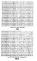
- the figure 1 is an enlargement a thousand times under microscope glass, after the step of selenization: the photo shows few defects, small size moreover. It is considered that the quality of the electrode is good.
- the figure 2 corresponds to a photo of an enlargement 1000 times using a microscope of this example 5, a portion of the layered glass after the selenization test: we see few defects, very small size. This is a snapshot quite comparable to the photo according to the figure 1 .
- Example 2 It corresponds to Example 2, with in addition a layer of TiN.
- Example 3 It corresponds to Example 3, with a layer of TiN in addition.
- the Si 3 N 4 barrier layers are effective, and prevent the deterioration of the sodium diffusion electrode, since in all the examples, the values of R (1) and R (2) are the same or almost the same. . They therefore also prevent the deterioration of the absorber layer type CIS.
- the molybdenum layer is in all these examples with a thickness of 400 nm or 500 nm. In terms of colorimetry on the glass side, it has no influence from the moment it is thick by at least 50 to 100 nm, since it is then a perfectly opaque mirror layer: the results would therefore be the same with a layer of Mo of 175 or 200 nm.
- the TiN layer being deposited by reactive sputtering in a reactive atmosphere containing 20% by volume of nitrogen.
- Example 8 has a slightly substoichiometric TiN layer, Example 8a has an approximately stoichiometric TiN layer, while Example 8ter tends to be superstoichiometric to nitrogen.
- the Si 3 N 4 barrier layer (refractive index of about 2) is associated with an additional layer based on SiO 2 (refractive index of about 1.45) to make a high optical coating. index / low index.
- the TiN layer is deposited in an atmosphere having 20% by volume of nitrogen.
- Example 9 is repeated, this time with 40% nitrogen in the TiN deposition atmosphere.
- Example 9 is repeated, this time with 70% nitrogen in the TiN deposition atmosphere.
- the NbN layer was deposited in an atmosphere containing 20% nitrogen.
- Example 10 is repeated, but here the NbN layer was deposited in an atmosphere containing 40% nitrogen.
- Example 10 is replicated, but here the NbN layer has been deposited in a atmosphere containing 70% nitrogen.
- the NbN is rather under or over-stoichiometric, the values of a * and b * are negative, which corresponds to an aesthetic blue-green color, whose intensity varies.
- This example shows the sequence of layers of Examples 10, 10bis, 10ter, but with different Si 3 N 4 and SiO 2 thicknesses.
- barrier layer in a high-index / low-index / high refractive index three-layer optical coating.
- This example has a color in blue-green, moreover not very intense.
Abstract
Description
- L'invention se rapporte à un substrat, notamment transparent, notamment en verre, qui est muni d'une électrode. Ce substrat conducteur est tout particulièrement destiné à faire partie de cellules solaires.
- En effet, de façon connue, les cellules solaires intègrent ce type de substrat conducteur, ensuite revêtu d'une couche d'agent absorbeur, généralement en chalcopyrite de cuivre Cu, d'indium In, et de sélénium Se et/ou de soufre S. Il peut s'agir, par exemple, d'un matériau du type CuInSe2. Ce type de matériau est connu sous l'abréviation CIS.
- Pour ce type d'application, les électrodes sont le plus souvent à base de molybdène Mo, car ce matériau présente un certain nombre d'avantages : c'est un bon conducteur électrique (résistance spécifique relativement faible de l'ordre de 5,2 mW.cm). Il peut être soumis aux traitements thermiques élevés nécessaires, car il a un point de fusion élevé (2610°C). Il résiste bien, dans une certaine mesure, au sélénium et au soufre. Le dépôt de la couche d'agent absorbeur impose le plus souvent un contact avec une atmosphère contenant du sélénium ou du soufre qui tend à détériorer la plupart des métaux. Au contraire, le molybdène réagit en surface, avec le sélénium notamment, formant du MoSe2. Mais il garde l'essentiel de ses propriétés, notamment électriques, et conserve un contact électrique adéquat avec la couche de CIS. Enfin, c'est un matériau qui adhère bien aux couches CIS, il tend même à en favoriser leur croissance cristalline.
- Cependant, il présente un inconvénient important quand on envisage une production industrielle : c'est un matériau coûteux. En effet, les couches en Mo sont habituellement déposées par pulvérisation cathodique (assistée par champ magnétique). Or les cibles de Mo sont onéreuses. Cela est d'autant moins négligeable que pour obtenir le niveau de conductivité électrique voulu (une résistance par carré inférieure à 2, et de préférence inférieure à 1 ou 0.5 ohm.carré après traitement dans une atmosphère contenant du S ou du Se), il faut une couche de Mo épaisse, généralement de l'ordre de 700 nm à 1 micromètre.
- L'invention a alors pour but l'obtention d'un substrat muni d'une électrode, destinée à des cellules solaires, qui soit d'une fabrication plus simple et/ou moins onéreuse que les électrodes de Mo connues, mais dont les performances, notamment électriques, soient équivalentes ou tout au moins suffisantes pour l'application envisagée.
- L'invention a tout d'abord pour objet un substrat, notamment transparent, notamment en verre, muni d'une électrode, notamment adaptée pour des cellules solaires, et qui comprend une couche conductrice à base de molybdène Mo d'au plus 500 nm, notamment d'au plus 400 ou d'au plus 300 ou d'au plus 200 nm. Elle a une épaisseur qui, de préférence, est d'au moins 20 nm, ou d'au moins 50 ou 80 ou 100 nm.
- Au sens de l'invention, on entend par couche soit une couche continue, soit une couche discontinue, présentant notamment des motifs (soit par gravure d'une couche continue, soit par dépôt directement de la couche discontinue au motif voulu, par un système de masque par exemple). Cela s'applique à toutes les couches dont il est question dans la présente demande.
- La démarche de l'invention n'a pas consisté à supprimer complètement le molybdène au profit d'un autre métal, car aucun n'a été jugé susceptible de résister suffisamment, notamment au contact avec le sélénium ou le soufre et aux traitements thermiques évoqué plus haut, sans dégradation importante (le problème de la dégradation possible du Mo touche de la même façon la couche d'agent absorbeur qui le recouvre). Par contre, la démarche a été de diminuer significativement l'épaisseur de molybdène : il s'est avéré, contre toutes attentes, que des épaisseurs bien inférieures à celles utilisées habituellement, bien inférieures à 1 micromètre, suffisaient tout-à-fait pour obtenir les performances électriques voulues, avec en conséquence un gain appréciable en termes de coût de matières premières. Diminuer l'épaisseur de la couche de molybdène présente un autre avantage: il s'est avéré que l'on pouvait se permettre de déposer ces couches relativement fines par pulvérisation cathodique avec des paramètres de dépôt conduisant à des couches fortement contraintes, sans les problèmes de délamination que l'on peut rencontrer dans ce cas-là avec des couches épaisses. Des couches plus minces tendent en outre à présenter moins de défauts connus sous le terme de "pinholes" (trous d'épingles).
- Pour garantir que des couches de molybdène plus minces gardent toute leur efficacité, l'invention a recours, de préférence, de façon alternative ou cumulative, à plusieurs variantes (qui restent cependant optionnelles).
- Selon une première variante, on insère avantageusement entre le substrat et l'électrode une couche dite couche-barrière. Sa fonction principale est de faire barrage à la migration d'espèces diffusantes hors du substrat vers l'électrode et jusqu'à la couche d'agent absorbeur (et éventuellement, réciproquement, des espèces diffusantes de l'électrode vers le substrat). Quand le substrat est en verre, les espèces susceptibles de diffuser hors du verre et de dégrader l'électrode et la couche d'agent absorbeur sont notamment les alcalins. Prévoir une telle couche-barrière permet d'utiliser comme substrat du verre standard silico-sodo-calcique obtenu par flottage, sans risquer de détériorer l'électrode, ni la couche d'agent absorbeur en chalcopyrite. Ceci est, dans le cadre de l'invention, d'autant plus important que la couche de molybdène est mince, et qu'une dégradation même sur une faible épaisseur aurait un impact plus important que sur une couche beaucoup plus épaisse.
- Cette couche-barrière, avantageusement, est à base de matériau diélectrique choisi parmi au moins l'un des composés suivantes : nitrure ou oxynitrure de silicium, nitrure ou oxynitrure d'aluminium, oxyde ou oxynitrure de silicium. Le nitrure de silicium (contenant éventuellement un métal minoritaire du type Al ou du bore) s'est avéré particulièrement efficace. C'est un matériau très inerte, peu sensible aux traitements thermiques et bloquant de manière satisfaisante la diffusion des alcalins.
- De préférence, la couche-barrière a une épaisseur d'au moins 20 nm, notamment d'au moins 100 nm ou 120 ou 150 nm, et une épaisseur d'au plus 300 nm, notamment d'au plus 250 ou 200 nm.
- Selon une seconde variante, on peut vouloir « compenser » la diminution d'épaisseur de la couche en Mo, pour obtenir une électrode qui, globalement, est aussi conductrice voire plus conductrice qu'une couche de Mo épaisse. La solution selon l'invention consiste à ajouter, dans l'électrode, à la couche à base de Mo, au moins une autre couche conductrice de nature différente. On choisit avantageusement cette ou ces couches conductrices « complémentaires » en des matériaux moins coûteux à déposer en couche mince que le molybdène (par pulvérisation cathodique).
- La couche conductrice complémentaire, ou l'ensemble des couches conductrices complémentaires s'il y en a plusieurs, a de préférence une épaisseur d'au moins 10 nm, notamment d'au moins 40 nm. De préférence, elle a une épaisseur d'au plus 300 nm, et on la choisit avantageusement dans une gamme allant de 50 à 200 ou 300 nm.
- Selon un premier mode de réalisation de cette seconde variante, l'électrode comprend au moins une couche conductrice complémentaire dite M à base de métal ou d'un alliage d'au moins deux métaux. Il peut s'agir, notamment des métaux ou alliages suivants : Cu, Ag, Al, Ta, Ni, Cr, NiCr, acier. On a avantage à disposer cette ou ces couches métalliques complémentaires en dessous de la couche à base de molybdène : dans cette configuration, la couche de molybdène isole ces couches métalliques du contact avec le sélénium ou le soufre, qui sont particulièrement corrosifs et auxquels le molybdène résiste de façon correcte.
- Selon un second mode de réalisation de la seconde variante, alternatif ou cumulatif avec le premier mode, l'électrode comprend au moins une couche conductrice complémentaire dite M'N à base d'un nitrure métallique ; il s'agit notamment d'un nitrure d'au moins un des métaux suivants : Ta, Zr, Nb, Ti, Mo, Hf. Cette couche peut être située en dessous ou au-dessus de la couche à base de molybdène (voire être au nombre de deux, l'une en dessous et l'autre au-dessus de ladite couche). Le nitrure peut être stoechiométrique, sous-stoechiométrique ou sur-stoechiométrique en azote. On peut ajuster la stoechiométrie, notamment en faisant varier le pourcentage d'azote dans la chambre de pulvérisation quand on dépose la couche par pulvérisation cathodique réactive à partir d'une cible métallique.
- Un mode de réalisation particulièrement avantageux consiste à cumuler les deux précédents, en prévoyant une couche M'N entre une couche M et la couche à base de Mo. Dans cette configuration, en effet, la couche de nitrure M'N joue non seulement le rôle de couche conductrice, mais également celui d'une couche venant empêcher (ou tout au moins diminuer significativement) toute interdiffusion d'espèces entre les deux couches métalliques (M et Mo). Ainsi, il s'est avéré que des couches de TiN, TaN, ZrN, NbN et MoN étaient efficaces pour empêcher la diffusion du cuivre vers la couche de molybdène. Il a été aussi montré que les couches de HfN étaient particulièrement efficaces pour empêcher la diffusion d'aluminium vers la couche de molybdène (ce type de formule HfN, etc... ne préjuge pas de la stoechiométrie du nitrure, il peut s'agir aussi d'un nitrure sous- ou sur-stoechiométrique, comme pour toutes les autres formules de nitrure mentionnées dans le présent texte).
- On peut avoir, par exemple, des configurations d'électrodes selon l'invention qui comprennent les séquences de couches suivantes :
- M/Mo/M'N
- M/M'N/Mo
- M/Mo
- M'N/Mo
- Mo/M'N
- Dans le cas où la couche de métal M est à base d'argent, il est préférable d'assurer sa bonne adhérence à la couche sous jacente (par exemple la couche-barrière du type Si3N4 dans une configuration :
- couche-barrière/couche M/couche M'N/couche Mo.
- De préférence, la somme des épaisseurs des couches conductrices de l'électrode est inférieure ou égale à 600 nm, notamment inférieure ou égale à 500 ou 400 nm.
- L'électrode a avantageusement une résistance par carré inférieure ou égale à 2Ω/, notamment inférieure ou égale à 1Ω/, de préférence inférieure ou égale à 0,50 ou 0,45Ω/ : ces valeurs sont appropriées pour des électrodes de cellule solaire.
- Selon une variante préférée, l'invention a cherché à améliorer l'aspect de la cellule solaire. En effet, quand la cellule solaire équipe des façades ou des toitures de bâtiment, son aspect « côté intérieur » du bâtiment (du côté extérieur, l'électrode fait un miroir) n'est pas toujours très esthétique. La colorimétrie en réflexion est susceptible d'amélioration.
- Une première solution à ce problème subsidiaire selon l'invention a consisté à inclure la couche-barrière précédemment évoquée dans un revêtement multicouches à but optique « sous » l'électrode à proprement dit. Le revêtement optique est constitué d'au moins deux couches de matériaux diélectriques d'indices de réfraction différents. En jouant sur les épaisseurs et les différences d'indices entre les couches, on peut ainsi régler assez finement la colorimétrie du substrat à couches en réflexion, par interférence.
- Ce revêtement, de préférence, comprend une alternance de couches à haut indice (1,9 à 2,3 par exemple) et des couches à bas indice (1,4 à 1,7 par exemple). Des modes de réalisation de ce revêtement sont, par exemple : Si3N4/SiO2 ou Si3N4/SiO2/Si3N4.
- Une seconde solution, alternative ou cumulative avec la première, consiste à utiliser des électrodes contenant au moins une couche à base de nitrure M'N et à modifier (légèrement) la stoechiométrie de l'azote. Il s'est en effet avéré que des nitrures légèrement sous-ou sur-stoechiométriques gardaient les mêmes propriétés électriques, mais permettaient de faire varier dans une certaine mesure la colorimétrie du substrat. En combinant les deux solutions, on augmente les possibilités d'ajustement de la colorimétrie.
- Une troisième solution, alternative ou cumulative avec l'une au moins des deux premières solutions, consiste à disposer sous l'électrode, notamment à interposer entre la couche-barrière et l'électrode, une fine couche absorbante dans le visible. Il peut par exemple s'agir de couches en nitrure de métal, du type TiN, et elles ont de préférence une épaisseur cantonnée à une gamme allant de 2 à 15 nm. On peut avoir ainsi une séquence de couches du type verre/ couche-barrière comme Si3N4/fine couche absorbante comme TiN/SiO2/Mo :dans ce cas, la couche absorbante se trouve "au milieu" du revêtement optique Si3N4/SiO2.
- On peut ainsi obtenir un substrat muni de ce revêtement et de l'électrode qui, en réflexion, a des valeurs de a* et b* négatives dans les systèmes de colorimétrie (L, a*, b*), ce qui correspond à des couleurs dans les bleus-verts, ou une valeur de a* légèrement positive et une valeur de b* négative, ce qui correspond à une couleur dans les rosés.
- L'invention a aussi pour objet le substrat précédemment défini et recouvert, au-dessus de l'électrode, par une couche d'agent absorbeur de chalcopyrite.
- Elle a aussi pour objet ledit substrat pour faire des cellules solaires.
- L'invention sera maintenant détaillée à l'aide d'exemples de réalisation, non limitatifs, d'électrodes pour cellules solaires illustrés aux
figures 1 et 2 par des photos d'agrandissement des verres à couches. - Chaque exemple utilise un substrat de verre silico-sodo-calcique clair de 2 mm d'épaisseur. (les verres ont généralement une épaisseur entre 1 et 4 ou entre 1 et 3 mm.)
- L'ensemble des couches est déposé sur les verres par pulvérisation cathodique assistée par champ magnétique :
- ™ les couches de métal à partir de la cible de métal correspondante, en atmosphère inerte,
- ™ les couches de nitrure de métal à partir de la cible de métal correspondante, en atmosphère réactive contenant un mélange de gaz inerte et d'azote,
- ™ les couches de nitrure de silicium à partir d'une cible de Si dopé (Al), en atmosphère réactive contenant un mélange de gaz inerte et d'azote,
- ™ les couches d'oxyde de silicium à partir d'une cible de Si (dopé Al) et d'une atmosphère réactive comprenant un mélange de gaz inerte et d'oxygène.
- Les couches sont testées de la façon suivante :
- ← - mesure de la résistance par carré R (1) par la méthode des quatre points après dépôt de toutes les couches,
- ↑ - test appelé « bronze test » : ce test consiste à chauffer le verre muni de toutes les couches à 350°C pendant 10 minutes à l'air. Il est destiné à vérifier s'il y a eu ou non diffusion du sodium du verre vers l'électrode. A la fin du test, on mesure la résistance par carré, R (2), toujours par la méthode des quatre points. On vérifie aussi au microscope (à des agrandissements x100 et x1000) si le traitement thermique a provoqué ou non des défauts (piqûres), ...
- → - test dit « test de sélénisation » : ce test consiste à chauffer à nouveau les verres munis de toutes les couches sous une atmosphère de sélénium pendant 10 minutes. La température du sélénium est entre 200 et 240°C, la température du verre est entre 325 et 365°C. A la fin du test, on mesure à nouveau la résistance par carré R (3) et on en déduit la différence de résistivité avant/après sélénisation Δ R (3).
- Il est à noter que ce test de sélénisation est en fait beaucoup plus "dur" qu'il ne l'est dans la réalité. En effet, l'invention est ici intéressée à ne fabriquer dans un premier temps que les électrodes. Cependant, quand on fabrique la cellule solaire dans son ensemble, cette étape de sélénisation se fait une fois la couche en CIS déposée : dans le cycle de fabrication normal d'une cellule solaire, l'électrode est « protégée » du contact direct avec le sélénium par la couche de chalcopyrite.
- Pour que les électrodes soient considérées comme satisfaisantes, il est jugé avantageux :
- ™ que le sodium du verre soit empêché de diffuser vers l'électrode,
- ™ que l'électrode ait une certaine résistance au « bronze test » et au « test de sélénisation » : peu de défauts, résistance par carré suffisante.
- ™ que l'électrode adhère bien aux couches du type CIS,
- ™ que l'électrode soit aisément gravable, notamment par laser.
- Cet exemple utilise une couche-barrière et une électrode mono-couche en molybdène, selon la séquence :
- Verre/Si3N4 (200 nm)/Mo (500 nm)
- La
figure 1 est un agrandissement à mille fois sous microscope du verre, après l'étape de sélénisation : la photo montre peu de défauts, de petite taille de surcroît. On considère que la qualité de l'électrode est bonne. - Cet exemple utilise le même empilement de couches qu'à l'exemple 1, mais avec une couche en Mo nettement plus mince, selon la séquence :
- Verre/Si3N4 (200nm)/Mo (200 nm)
- Cet exemple utilise une couche-barrière, et une électrode bi-couche, couche de métal M puis couche Mo, selon la séquence suivante :
- Verre/Si3N4 (200 nm)/Ag (50 nm)/Mo (175 nm)
- Cet exemple utilise la même configuration que l'exemple 2 , mais avec un autre type de couche métal M :
- Verre/Si3N4 (200 nm)/Al (100 nm)/Mo (175 nm)
- Cet exemple utilise une couche-barrière et une électrode tri-couche métal/nitrure métallique/Mo selon la séquence :
- Verre/Si3N4 (200 nm)/Cu (100 nm)/TiN (100 nm)/Mo (175 nm)
- C'est la même configuration que l'exemple 4, avec une épaisseur différente pour la couche de cuivre :
- Verre/Si3N4 (200 nm)/Cu (50 nm)/TiN (100 nm)/Mo (175 nm)
- La
figure 2 correspond à une photo d'un agrandissement 1000 fois à l'aide d'un microscope de cet exemple 5, d'une portion du verre à couches après le test de sélénisation : on voit peu de défauts, de taille très petite. C'est un cliché tout-à-fait comparable à la photo selon lafigure 1 . - Cet exemple utilise une couche-barière et une électrode tri-couche, selon la séquence suivante :
- Verre/Si3N4 (200 nm)/Ag (50 nm)/TiN (100 nm)/Mo (175 nm)
- Il correspond à l'exemple 2, avec en plus une couche de TiN.
- Cet exemple utilise toujours une couche-barrière et une électrode tri-couche, selon la séquence suivante :
- Verre/Si3N4 (200 nm)/Al (100 nm)/TiN (100 nm)/Mo (175 nm)
- Il correspond à l'exemple 3, avec une couche de TiN en plus.
- La tableau 1 ci-dessous regroupe, pour chacun des exemples 1 à 7, les valeurs de R (1), R (2), l'évaluation des défauts après le bronze test (" défauts ", et ΔR (3), ces termes ayant été explicités plus haut.
TABLEAU 1 EXEMPLES R (1) R (2) DEFAUTS Δ R (3), Ex. 1 0.37 0.37 Aucun 0 à - 5 % Si3N4/Mo Ex. 1 bis 0.98 0.96 Aucun 0 à - 3% Si3N4/Mo Ex. 2 0.42 0.42 Aucun -17% Si3N4/Ag/Mo Ex. 3 0.36 0.34 Aucun - Si3N4/Al/Mo Ex. 4 0.45 0.45 Aucun -9% Si3N4/Cu/TiN/Mo Ex. 5 0.44 0.44 Aucun - 10 % Si3N4/Cu/TiN/Mo Ex. 6 0.44 0.44 Aucun - 12 % Si3N4/Ag/TiN/Mo Ex. 7 0.38 0.36 Aucun - Si3N4/Al/TiN/Mo - De ces données peuvent être tirées les conclusions suivantes :
- On peut obtenir une valeur de R nettement inférieure à 1 ohm/carré avec moins de 200 nm de molybdène, que l'on associe avec une couche de nitrure métallique et/ou de métal d'épaisseurs raisonnables (en tout, les électrodes bi ou tri-couches restent d'une épaisseur globale inférieure à 400 ou 500 nm).
- Les couches-barrières en Si3N4 sont efficaces, et empêchent la détérioration de l'électrode par diffusion du sodium, puisque dans tous les exemples, les valeurs de R (1) et R (2) sont les mêmes ou quasiment les mêmes. Elles empêchent donc également la détérioration de la couche d'agent absorbeur type CIS.
- On peut choisir aussi d'avoir une électrode mono-couche en Mo (exemple 1, avec 500 nm et associée à une couche-barrière. Elle donne de bons résultats: On peut encore avoir une résistance par carré inférieure à 1 ohm.carré avec une électrode composée seulement de 200 nm de Mo. Cela prouve qu'il est inutile d'avoir recours à une couche de Mo bien plus épaisse comme cela a pu se faire jusqu'ici.
- Ces exemples ont pour but d'ajuster la colorimétrie de l'électrode en réflexion.
- La couche de molybdène est dans tous ces exemples d'une épaisseur de 400 nm ou 500 nm. Sur le plan de la colorimétrie côté verre, elle n'a pas d'influence à partir du moment où elle est épaisse d'au moins 50 à 100 nm, puisqu'elle est alors une couche-miroir parfaitement opaque : les résultats seraient donc les mêmes avec une couche de Mo de 175 ou 200 nm.
- Cet exemple utilise l'empilement suivant :
- Verre/Si3N4 (200 nm)/TiN (100 nm)/Mo (400 nm)
- La couche de TiN étant déposée par pulvérisation réactive dans une atmosphère réactive contenant 20 % en volume d'azote.
- Il s'agit de la même configuration qu'à l'exemple 8, mais ici la couche de TiN a été déposée dans une atmosphère contenant 40 % d'azote.
- Il s'agit de la même configuration qu'à l'exemple 8, mais ici la couche de TiN a été déposée dans une atmosphère contenant 70 % d'azote.
- Le tableau ci-dessous regroupe pour ces trois exemples des valeurs de a* et b*, selon le système de colorimétrie (L, a*, b*) mesurées côté verre, ainsi que les valeurs de R (mesures faites avant le « bronze » test)
EXEMPLES a* b* R (ohm.carré) Ex. 8 - 8,6 19,4 0,44 Ex. 8bis -9,2 1,5 0,38 Ex. 8ter -11,6 -3,6 0,35 - On constate que la variation dans la stoechiométrie au TiN (en fonction du taux de N2 lors du dépôt) ne modifie pas significativement les propriétés électriques de l'électrode. Par contre, elle permet de modifier beaucoup les valeurs de a*, et, plus encore, de b*: l'exemple 8 est ainsi coloré dans les rouges, avec un b* très positif, alors que l'exemple 8ter est dans les bleus-verts, avec un b* légèrement négatif.
- L'exemple 8 a une couche de TiN légèrement sous-stoechiométrique, l'exemple 8bis a une couche de TiN approximativement stoechiométrique, tandis que l'exemple 8ter a tendance à être sur-stoechiométrique en azote.
- Dans cet exemple, la couche-barrière en Si3N4 (indice de réfraction d'environ 2) est associée à une couche supplémentaire à base de SiO2 (indice de réfraction d'environ 1,45) pour faire un revêtement optique haut indice/bas indice.
- La configuration est la suivante :
- Verre/Si3N4 (200 nm)/SiO2 (20 nm)/TiN (100 nm)/Mo (400 nm)
- La couche de TiN est déposée dans une atmosphère ayant 20 % en volume d'azote.
- On réplique l'exemple 9, avec cette fois 40 % d'azote dans l'atmosphère de dépôt du TiN.
- On réplique l'exemple 9, avec cette fois 70 % d'azote dans l'atmosphère de dépôt du TiN.
- Le tableau ci-dessous regroupe pour ces 3 exemples, les valeurs de a*, b* et Rcarré explicitées plus haut.
EXEMPLES a* b* R (ohm.carré) Ex. 9 - 8,1 22,5 0,34 Ex. 9bis -10,6 -8,3 0,38 Ex. 9ter -14,0 5,5 0,35 - Cette fois, la couche de nitrure utilisée est en NbN, selon la configuration suivante :
- Verre/Si3N4 (200 nm)/SiO2 (30 nm/NbN (100 nm)/Mo (500 nm)
- La couche de NbN a été déposée dans une atmosphère contenant 20 % d'azote.
- On réplique l'exemple 10, mais ici la couche de NbN a été déposée dans une atmosphère contenant 40 % d'azote.
- On réplique l'exemple 10, mais ici la couche de NbN a été déposée dans une atmosphère contenant 70 % d'azote.
- Le tableau ci-dessous regroupe pour ces trois exemples les valeurs de a*, b* et Rcarré déjà explicitées :
EXEMPLES a* b* R (ohm/carré) Ex. 10 -14 -0,5 0,29 Ex. 10bis -10,6 -9,2 0,37 Ex. 10ter -17,6 -0,9 0,42 - Ici, que le NbN soit plutôt sous ou sur-stoechiométrique, les valeurs de a* et b* sont négatives, ce qui correspond à une couleur bleu-verte esthétique, dont l'intensité varie.
- Cet exemple reprend la séquence de couches des exemples 10, 10bis, 10ter, mais avec des épaisseurs de Si3N4 et de SiO2 différentes.
- La configuration est la suivante :
- Verre/Si3N4 (150 nm)/SiO2 (90 nm)/NbN (100 nm)/Mo (500 nm)
- Cet exemple réplique l'exemple 11, mais ici la couche de NbN a été déposée dans une atmosphère contenant 40 % d'azote.
- Cet exemple réplique l'exemple 11, mais ici la couche de NbN a été déposée dans une atmosphère contenant 70 % d'azote.
- Le tableau ci-dessous regroupe pour ces trois exemples les valeurs de a*, b* et Rcarré déjà explicitées :
EXEMPLES a* b* R (ohm/carré) Ex. 11 0,3 -7,6 0,34 Ex. 11 bis 2,8 -10,3 0,33 Ex. 11 ter 8,8 -14,2 0,28 - Ces exemples sont donc dans les rosés, couleur également jugée esthétique.
- Cet exemple présente la séquence de couches suivante :
- Verre/ Si3N4 (150 nm)/SiO2 (65 nm)/Si3N4 (15 nm)/Mo (500nm)
- Il intègre donc la couche-barrière dans un revêtement optique à trois couches haut indice/bas indice/haut indice de réfraction.
- Le tableau ci-dessous reprend les mêmes données pour cet exemple que dans les exemples précédents.
EXEMPLE a* b* R (ohm/carré) Ex. 12 - 4.1 -6.3 0,28 - Cet exemple a donc une couleur dans les bleus-verts, de surcroît peu intense.
- En conclusion, on peut donc ajuster finement la couleur des électrodes selon l'invention en jouant sur la stoechiométrie de la couche de nitrure et/ou en ajoutant un filtre à au moins deux couches incluant avantageusement la couche-barrière. On a par ailleurs vérifié que les valeurs de a* et b* de cette seconde série d'exemples variaient peu (moins de ± 2) une fois passé le « bronze » test.
Claims (15)
- Substrat, notamment transparent, notamment en verre, muni d'une électrode, notamment pour cellule solaire, caractérisé en ce que l'électrode comprend une couche conductrice à base de molybdène Mo d'au plus 500 nm d'épaisseur, notamment d'au plus 400 nm ou d'au plus 300 nm ou d'au plus 200 nm, en ce que le substrat est muni d'au moins une couche-barrière, notamment vis-à-vis des alcalins, insérée entre ledit substrat et ladite électrode, et en ce que la couche-barrière fait partie d'un revêtement multicouches à but optique, constitué d'au moins deux couches de matériaux diélectriques d'indices de réfraction différents.
- Substrat selon la revendication 1, caractérisé en ce que le revêtement multicouches à but optique comporte une alternance de couches à haut indice de réfraction, compris entre 1,9 et 2,3, et de couches à bas indice de réfraction, compris entre 1,4 et 1,7, notamment selon les séquences Si3N4/SiO2 ou Si3N4/SiO2/Si3N4.
- Substrat selon la revendication 1 ou 2, caractérisé en ce que la couche-barrière est à base de matériau diélectrique, choisi parmi au moins l'un des composés suivants : nitrure ou oxynitrure de silicium, nitrure ou oxynitrure d'aluminium, oxyde ou oxycarbure de silicium.
- Substrat selon l'une des revendications précédentes, caractérisé en ce que la couche-barrière a une épaisseur d'au moins 20 nm, notamment d'au moins 100 nm, et de préférence d'au plus 300 nm, notamment d'au plus 250 ou 200 nm.
- Substrat selon l'une des revendications précédentes, caractérisé en ce que la composition du revêtement optique règle au moins en partie la colorimétrie en réflexion du substrat, notamment dans les bleus-verts avec des valeurs de a* et de b* négatives ou dans les rosés avec des valeurs de a* légèrement positives et des valeurs de b* négatives.
- Substrat selon l'une des revendications précédentes, caractérisé en ce que la couche à base de molybdène a une épaisseur d'au moins 20 nm, notamment d'au moins 50 ou 80 nm.
- Substrat selon l'une des revendications précédentes, caractérisé en ce que l'électrode comprend au moins une couche conductrice complémentaire M'N à base d'un nitrure sous-stoechiométrique, stoechiométrique ou sur-stoechiométrique, en azote, d'au moins un des métaux suivants : Ta, Zr, Nb, Ti, Mo, Hf.
- Substrat selon la revendication 7, caractérisé en ce que la couche M'N est en-dessous de la couche à base de molybdène Mo.
- Substrat selon la revendication 8, caractérisé en ce que la stoechiométrie en azote de la couche en nitrure M'N règle au moins en partie la colorimétrie en réflexion du substrat, notamment dans les bleus-verts avec des valeurs de a* et b* négatives ou dans les rosés avec des valeurs de a* positives et des valeurs de b* négatives.
- Substrat selon la revendication 9, caractérisé en ce qu'une fine couche absorbante dans le visible, notamment en TiN et de préférence d'une épaisseur de 2 à 15 nm, est insérée entre la couche-barrière et l'électrode, de façon à régler, au moins en partie, la colorimétrie en réflexion du substrat, notamment dans les bleus-verts avec des valeurs de a* et b* négatives, ou dans les rosés avec des valeurs de a* légèrement positives et des valeurs de b* négatives.
- Substrat selon l'une des revendications précédentes, caractérisé en ce que la somme des épaisseurs des couches conductrices de l'électrode est inférieure ou égale à 600 nm, notamment inférieure ou égale à 500 nm.
- Substrat selon l'une des revendications précédentes, caractérisé en ce que l'électrode a une résistance par carré R inférieure ou égale à 2Ω/, notamment inférieure ou égale à 1Ω/, de préférence inférieure ou égale à 0,50 ou 0,45Ω/.
- Substrat selon l'une des revendications précédentes, caractérisé en ce qu'il comprend au-dessus de l'électrode une couche d'agent absorbeur de chalcopyrite.
- Utilisation du substrat selon la revendication 13 pour faire une cellule solaire.
- Cellule solaire, caractérisée en ce qu'elle comprend le substrat selon la revendication 13.
Applications Claiming Priority (2)
| Application Number | Priority Date | Filing Date | Title |
|---|---|---|---|
| FR0101292A FR2820241B1 (fr) | 2001-01-31 | 2001-01-31 | Substrat transparent muni d'une electrode |
| EP02700381A EP1356528A1 (fr) | 2001-01-31 | 2002-01-23 | Sustrat transparent muni d'une electrode |
Related Parent Applications (2)
| Application Number | Title | Priority Date | Filing Date |
|---|---|---|---|
| EP02700381A Division EP1356528A1 (fr) | 2001-01-31 | 2002-01-23 | Sustrat transparent muni d'une electrode |
| EP02700381.3 Division | 2002-01-23 |
Publications (3)
| Publication Number | Publication Date |
|---|---|
| EP2369635A2 true EP2369635A2 (fr) | 2011-09-28 |
| EP2369635A3 EP2369635A3 (fr) | 2014-10-08 |
| EP2369635B1 EP2369635B1 (fr) | 2017-06-14 |
Family
ID=8859441
Family Applications (5)
| Application Number | Title | Priority Date | Filing Date |
|---|---|---|---|
| EP02700381A Withdrawn EP1356528A1 (fr) | 2001-01-31 | 2002-01-23 | Sustrat transparent muni d'une electrode |
| EP11170582.8A Expired - Lifetime EP2369633B1 (fr) | 2001-01-31 | 2002-01-23 | Substrat transparent muni d'une electrode |
| EP11170584.4A Withdrawn EP2369634A3 (fr) | 2001-01-31 | 2002-01-23 | Substrat transparent muni d'une electrode |
| EP11170586.9A Withdrawn EP2369636A3 (fr) | 2001-01-31 | 2002-01-23 | Substrat transparent muni d'une electrode |
| EP11170585.1A Expired - Lifetime EP2369635B1 (fr) | 2001-01-31 | 2002-01-23 | Substrat transparent muni d'une électrode |
Family Applications Before (4)
| Application Number | Title | Priority Date | Filing Date |
|---|---|---|---|
| EP02700381A Withdrawn EP1356528A1 (fr) | 2001-01-31 | 2002-01-23 | Sustrat transparent muni d'une electrode |
| EP11170582.8A Expired - Lifetime EP2369633B1 (fr) | 2001-01-31 | 2002-01-23 | Substrat transparent muni d'une electrode |
| EP11170584.4A Withdrawn EP2369634A3 (fr) | 2001-01-31 | 2002-01-23 | Substrat transparent muni d'une electrode |
| EP11170586.9A Withdrawn EP2369636A3 (fr) | 2001-01-31 | 2002-01-23 | Substrat transparent muni d'une electrode |
Country Status (12)
| Country | Link |
|---|---|
| US (3) | US8148631B2 (fr) |
| EP (5) | EP1356528A1 (fr) |
| JP (3) | JP4537000B2 (fr) |
| KR (1) | KR100949600B1 (fr) |
| CN (1) | CN1327533C (fr) |
| AU (1) | AU2002233459A1 (fr) |
| BR (1) | BR0206785A (fr) |
| ES (1) | ES2627686T3 (fr) |
| FR (1) | FR2820241B1 (fr) |
| MX (1) | MXPA03006682A (fr) |
| PT (1) | PT2369633T (fr) |
| WO (1) | WO2002065554A1 (fr) |
Cited By (1)
| Publication number | Priority date | Publication date | Assignee | Title |
|---|---|---|---|---|
| EP2800145A1 (fr) * | 2013-05-03 | 2014-11-05 | Saint-Gobain Glass France | Substrat de contact arrière pour module ou cellule photovoltaïque |
Families Citing this family (100)
| Publication number | Priority date | Publication date | Assignee | Title |
|---|---|---|---|---|
| US20090111206A1 (en) | 1999-03-30 | 2009-04-30 | Daniel Luch | Collector grid, electrode structures and interrconnect structures for photovoltaic arrays and methods of manufacture |
| US8138413B2 (en) | 2006-04-13 | 2012-03-20 | Daniel Luch | Collector grid and interconnect structures for photovoltaic arrays and modules |
| US8222513B2 (en) | 2006-04-13 | 2012-07-17 | Daniel Luch | Collector grid, electrode structures and interconnect structures for photovoltaic arrays and methods of manufacture |
| US8664030B2 (en) | 1999-03-30 | 2014-03-04 | Daniel Luch | Collector grid and interconnect structures for photovoltaic arrays and modules |
| US7507903B2 (en) | 1999-03-30 | 2009-03-24 | Daniel Luch | Substrate and collector grid structures for integrated series connected photovoltaic arrays and process of manufacture of such arrays |
| US8198696B2 (en) | 2000-02-04 | 2012-06-12 | Daniel Luch | Substrate structures for integrated series connected photovoltaic arrays and process of manufacture of such arrays |
| JP3910072B2 (ja) * | 2002-01-30 | 2007-04-25 | 東洋アルミニウム株式会社 | ペースト組成物およびそれを用いた太陽電池 |
| WO2004032189A2 (fr) * | 2002-09-30 | 2004-04-15 | Miasolé | Appareil et procede de fabrication conçus pour produire a grande echelle de cellules solaires a film mince |
| US8623448B2 (en) | 2004-02-19 | 2014-01-07 | Nanosolar, Inc. | High-throughput printing of semiconductor precursor layer from chalcogenide microflake particles |
| US20070163641A1 (en) * | 2004-02-19 | 2007-07-19 | Nanosolar, Inc. | High-throughput printing of semiconductor precursor layer from inter-metallic nanoflake particles |
| US8372734B2 (en) * | 2004-02-19 | 2013-02-12 | Nanosolar, Inc | High-throughput printing of semiconductor precursor layer from chalcogenide nanoflake particles |
| US7604843B1 (en) | 2005-03-16 | 2009-10-20 | Nanosolar, Inc. | Metallic dispersion |
| US7663057B2 (en) * | 2004-02-19 | 2010-02-16 | Nanosolar, Inc. | Solution-based fabrication of photovoltaic cell |
| US20070163642A1 (en) * | 2004-02-19 | 2007-07-19 | Nanosolar, Inc. | High-throughput printing of semiconductor precursor layer from inter-metallic microflake articles |
| US8329501B1 (en) | 2004-02-19 | 2012-12-11 | Nanosolar, Inc. | High-throughput printing of semiconductor precursor layer from inter-metallic microflake particles |
| US20060060237A1 (en) * | 2004-09-18 | 2006-03-23 | Nanosolar, Inc. | Formation of solar cells on foil substrates |
| US20070163639A1 (en) * | 2004-02-19 | 2007-07-19 | Nanosolar, Inc. | High-throughput printing of semiconductor precursor layer from microflake particles |
| US8846141B1 (en) | 2004-02-19 | 2014-09-30 | Aeris Capital Sustainable Ip Ltd. | High-throughput printing of semiconductor precursor layer from microflake particles |
| US7605328B2 (en) * | 2004-02-19 | 2009-10-20 | Nanosolar, Inc. | Photovoltaic thin-film cell produced from metallic blend using high-temperature printing |
| US20070169809A1 (en) * | 2004-02-19 | 2007-07-26 | Nanosolar, Inc. | High-throughput printing of semiconductor precursor layer by use of low-melting chalcogenides |
| US7700464B2 (en) * | 2004-02-19 | 2010-04-20 | Nanosolar, Inc. | High-throughput printing of semiconductor precursor layer from nanoflake particles |
| US8309163B2 (en) * | 2004-02-19 | 2012-11-13 | Nanosolar, Inc. | High-throughput printing of semiconductor precursor layer by use of chalcogen-containing vapor and inter-metallic material |
| JP4695850B2 (ja) * | 2004-04-28 | 2011-06-08 | 本田技研工業株式会社 | カルコパイライト型太陽電池 |
| US7838868B2 (en) | 2005-01-20 | 2010-11-23 | Nanosolar, Inc. | Optoelectronic architecture having compound conducting substrate |
| US20090032108A1 (en) * | 2007-03-30 | 2009-02-05 | Craig Leidholm | Formation of photovoltaic absorber layers on foil substrates |
| JP2008514006A (ja) * | 2004-09-18 | 2008-05-01 | ナノソーラー インコーポレイテッド | 箔基板上の太陽電池の形成 |
| US7276724B2 (en) | 2005-01-20 | 2007-10-02 | Nanosolar, Inc. | Series interconnected optoelectronic device module assembly |
| US7732229B2 (en) | 2004-09-18 | 2010-06-08 | Nanosolar, Inc. | Formation of solar cells with conductive barrier layers and foil substrates |
| US8541048B1 (en) | 2004-09-18 | 2013-09-24 | Nanosolar, Inc. | Formation of photovoltaic absorber layers on foil substrates |
| JP4663300B2 (ja) * | 2004-11-18 | 2011-04-06 | 本田技研工業株式会社 | カルコパイライト型薄膜太陽電池の製造方法 |
| JP2006165386A (ja) * | 2004-12-09 | 2006-06-22 | Showa Shell Sekiyu Kk | Cis系薄膜太陽電池及びその作製方法 |
| JP4664060B2 (ja) * | 2004-12-21 | 2011-04-06 | 本田技研工業株式会社 | カルコパイライト型太陽電池 |
| US8927315B1 (en) | 2005-01-20 | 2015-01-06 | Aeris Capital Sustainable Ip Ltd. | High-throughput assembly of series interconnected solar cells |
| JP4969785B2 (ja) * | 2005-02-16 | 2012-07-04 | 本田技研工業株式会社 | カルコパイライト型太陽電池及びその製造方法 |
| JP3963924B2 (ja) * | 2005-07-22 | 2007-08-22 | 本田技研工業株式会社 | カルコパイライト型太陽電池 |
| JP2007096031A (ja) * | 2005-09-29 | 2007-04-12 | Showa Shell Sekiyu Kk | Cis系薄膜太陽電池モジュール及びその製造方法 |
| JP4918247B2 (ja) | 2005-10-31 | 2012-04-18 | 昭和シェル石油株式会社 | Cis系薄膜太陽電池モジュール及びその製造方法 |
| US8389852B2 (en) * | 2006-02-22 | 2013-03-05 | Guardian Industries Corp. | Electrode structure for use in electronic device and method of making same |
| US9236512B2 (en) | 2006-04-13 | 2016-01-12 | Daniel Luch | Collector grid and interconnect structures for photovoltaic arrays and modules |
| US8729385B2 (en) | 2006-04-13 | 2014-05-20 | Daniel Luch | Collector grid and interconnect structures for photovoltaic arrays and modules |
| US8884155B2 (en) | 2006-04-13 | 2014-11-11 | Daniel Luch | Collector grid and interconnect structures for photovoltaic arrays and modules |
| US9006563B2 (en) | 2006-04-13 | 2015-04-14 | Solannex, Inc. | Collector grid and interconnect structures for photovoltaic arrays and modules |
| US8822810B2 (en) | 2006-04-13 | 2014-09-02 | Daniel Luch | Collector grid and interconnect structures for photovoltaic arrays and modules |
| US9865758B2 (en) | 2006-04-13 | 2018-01-09 | Daniel Luch | Collector grid and interconnect structures for photovoltaic arrays and modules |
| US9147778B2 (en) * | 2006-11-07 | 2015-09-29 | First Solar, Inc. | Photovoltaic devices including nitrogen-containing metal contact |
| US20080302413A1 (en) * | 2007-03-30 | 2008-12-11 | Craig Leidholm | Formation of photovoltaic absorber layers on foil substrates |
| FR2922046B1 (fr) | 2007-10-05 | 2011-06-24 | Saint Gobain | Perfectionnements apportes a des elements capables de collecter de la lumiere |
| FR2924863B1 (fr) * | 2007-12-07 | 2017-06-16 | Saint Gobain | Perfectionnements apportes a des elements capables de collecter de la lumiere. |
| AT10578U1 (de) * | 2007-12-18 | 2009-06-15 | Plansee Metall Gmbh | Dunnschichtsolarzelle mit molybdan-haltiger ruckelektrodenschicht |
| US8981211B2 (en) * | 2008-03-18 | 2015-03-17 | Zetta Research and Development LLC—AQT Series | Interlayer design for epitaxial growth of semiconductor layers |
| US20090260678A1 (en) * | 2008-04-16 | 2009-10-22 | Agc Flat Glass Europe S.A. | Glass substrate bearing an electrode |
| US20100180927A1 (en) * | 2008-08-27 | 2010-07-22 | Stion Corporation | Affixing method and solar decal device using a thin film photovoltaic and interconnect structures |
| DE202008018125U1 (de) | 2008-09-08 | 2011-12-27 | Saint-Gobain Glass France | Verbesserungen an Elementen, die Licht aufnehmen können |
| US8115095B2 (en) * | 2009-02-20 | 2012-02-14 | Miasole | Protective layer for large-scale production of thin-film solar cells |
| JP2010212336A (ja) * | 2009-03-09 | 2010-09-24 | Fujifilm Corp | 光電変換素子とその製造方法、及び太陽電池 |
| US8134069B2 (en) | 2009-04-13 | 2012-03-13 | Miasole | Method and apparatus for controllable sodium delivery for thin film photovoltaic materials |
| US8247243B2 (en) | 2009-05-22 | 2012-08-21 | Nanosolar, Inc. | Solar cell interconnection |
| JP2010282997A (ja) * | 2009-06-02 | 2010-12-16 | Seiko Epson Corp | 太陽電池、太陽電池の製造方法 |
| CN101931011A (zh) * | 2009-06-26 | 2010-12-29 | 安泰科技股份有限公司 | 薄膜太阳能电池及其基带和制备方法 |
| JP5114683B2 (ja) * | 2009-09-07 | 2013-01-09 | 新日鐵住金株式会社 | 太陽電池用ガラス基板の裏面電極及びその製造方法 |
| US20110067998A1 (en) * | 2009-09-20 | 2011-03-24 | Miasole | Method of making an electrically conductive cadmium sulfide sputtering target for photovoltaic manufacturing |
| US20110162696A1 (en) * | 2010-01-05 | 2011-07-07 | Miasole | Photovoltaic materials with controllable zinc and sodium content and method of making thereof |
| US20110259395A1 (en) * | 2010-04-21 | 2011-10-27 | Stion Corporation | Single Junction CIGS/CIS Solar Module |
| FR2961954B1 (fr) * | 2010-06-25 | 2012-07-13 | Saint Gobain | Cellule comprenant un materiau photovoltaique a base de cadmium |
| JP5667027B2 (ja) * | 2010-11-02 | 2015-02-12 | 富士フイルム株式会社 | 太陽電池サブモジュール及びその製造方法、電極付き基板 |
| FR2969389A1 (fr) | 2010-12-21 | 2012-06-22 | Saint Gobain | Substrat conducteur a base de molybdène |
| KR101219948B1 (ko) * | 2011-01-27 | 2013-01-21 | 엘지이노텍 주식회사 | 태양광 발전장치 및 제조방법 |
| GB201101910D0 (en) * | 2011-02-04 | 2011-03-23 | Pilkington Group Ltd | Growth layer for the photovol taic applications |
| FR2977078B1 (fr) * | 2011-06-27 | 2013-06-28 | Saint Gobain | Substrat conducteur pour cellule photovoltaique |
| US8642884B2 (en) * | 2011-09-09 | 2014-02-04 | International Business Machines Corporation | Heat treatment process and photovoltaic device based on said process |
| FR2982422B1 (fr) | 2011-11-09 | 2013-11-15 | Saint Gobain | Substrat conducteur pour cellule photovoltaique |
| US10043921B1 (en) | 2011-12-21 | 2018-08-07 | Beijing Apollo Ding Rong Solar Technology Co., Ltd. | Photovoltaic cell with high efficiency cigs absorber layer with low minority carrier lifetime and method of making thereof |
| DE102012205375A1 (de) * | 2012-04-02 | 2013-10-02 | Robert Bosch Gmbh | Mehrschicht-Rückelektrode für eine photovoltaische Dünnschichtsolarzelle, Verwen-dung der Mehrschicht-Rückelektrode für die Herstellung von Dünnschichtsolarzellen und -modulen, photovoltaische Dünnschichtsolarzellen und -module enthaltend die Mehrschicht-Rückelektrode sowie ein Verfahren zur Herstellung photovoltaischer Dünnschichtsolarzellen und -module |
| DE102012205378A1 (de) * | 2012-04-02 | 2013-10-02 | Robert Bosch Gmbh | Verfahren zur Herstellung von Dünnschichtsolarmodulen sowie nach diesem Verfahren erhältliche Dünnschichtsolarmodule |
| DE102012205377A1 (de) * | 2012-04-02 | 2013-10-02 | Robert Bosch Gmbh | Mehrschicht-Rückelektrode für eine photovoltaische Dünnschichtsolarzelle, Verwendung der Mehrschicht-Rückelektrode für die Herstellung von Dünnschichtsolarzellen und -modulen, photovoltaische Dünnschichtsolarzellen und -module enthaltend die Mehrschicht-Rückelektrode sowie ein Verfahren zur Herstellung photovoltaischer Dünnschichtsolarzellen und -module |
| US9246025B2 (en) * | 2012-04-25 | 2016-01-26 | Guardian Industries Corp. | Back contact for photovoltaic devices such as copper-indium-diselenide solar cells |
| US9159850B2 (en) * | 2012-04-25 | 2015-10-13 | Guardian Industries Corp. | Back contact having selenium blocking layer for photovoltaic devices such as copper—indium-diselenide solar cells |
| US9419151B2 (en) | 2012-04-25 | 2016-08-16 | Guardian Industries Corp. | High-reflectivity back contact for photovoltaic devices such as copper—indium-diselenide solar cells |
| US8809674B2 (en) | 2012-04-25 | 2014-08-19 | Guardian Industries Corp. | Back electrode configuration for electroplated CIGS photovoltaic devices and methods of making same |
| US9935211B2 (en) | 2012-04-25 | 2018-04-03 | Guardian Glass, LLC | Back contact structure for photovoltaic devices such as copper-indium-diselenide solar cells |
| WO2013190898A1 (fr) * | 2012-06-19 | 2013-12-27 | 富士電機株式会社 | Élément de conversion photoélectrique de chalcopyrite, électrode arrière et procédé de production de ceux-ci |
| US9871155B2 (en) | 2012-06-20 | 2018-01-16 | Bengbu Design & Research Institute For Glass Industry | Layer system for thin-film solar cells having an NaxIn1SyClz buffer layer |
| WO2013189976A1 (fr) | 2012-06-20 | 2013-12-27 | Saint-Gobain Glass France | Système multicouche pour cellules solaires à films minces |
| EP2865012B1 (fr) | 2012-06-20 | 2023-01-18 | Cnbm Research Institute For Advanced Glass Materials Group Co., Ltd. | Système à couches pour cellules solaires à couche mince |
| ES2441428B1 (es) | 2012-07-04 | 2016-02-05 | Abengoa Solar New Technologies, S.A. | Formulación de tintas con base de nanopartículas cerámicas |
| JP2014049571A (ja) * | 2012-08-30 | 2014-03-17 | Toyota Central R&D Labs Inc | 光電素子 |
| WO2014175451A1 (fr) * | 2013-04-26 | 2014-10-30 | コニカミノルタ株式会社 | Conducteur transparent et dispositif électronique |
| EP2800144A1 (fr) * | 2013-05-03 | 2014-11-05 | Saint-Gobain Glass France | Substrat de contact arrière pour module ou cellule photovoltaïque |
| EP2800146A1 (fr) | 2013-05-03 | 2014-11-05 | Saint-Gobain Glass France | Substrat de contact arrière pour module ou cellule photovoltaïque |
| US20160163905A1 (en) | 2013-06-27 | 2016-06-09 | Saint-Gobain Glass France | Layer system for thin-film solar cells having a sodium indium sulfide buffer layer |
| EP2871681A1 (fr) | 2013-11-07 | 2015-05-13 | Saint-Gobain Glass France | Substrat conducteur à contact arrière pour une cellule photovoltaïque ou module |
| FR3013507B1 (fr) * | 2013-11-15 | 2015-11-20 | Saint Gobain | Substrat de contact arriere pour cellule photovoltaique |
| CN103966565A (zh) * | 2013-12-13 | 2014-08-06 | 云南师范大学 | 一种用于彩色薄膜太阳电池表面涂层的制备方法 |
| EP2887405A1 (fr) | 2013-12-23 | 2015-06-24 | Saint-Gobain Glass France | Système à couches pour cellules solaires à couche mince |
| WO2017047366A1 (fr) * | 2015-09-18 | 2017-03-23 | 旭硝子株式会社 | Substrat de verre pour cellules solaires, et cellule solaire |
| DE202015106923U1 (de) | 2015-12-18 | 2016-01-22 | Saint-Gobain Glass France | Elektronisch leitfähiges Substrat für Photovoltaikzellen |
| FR3080221B1 (fr) * | 2018-04-11 | 2020-03-13 | Sunpartner Technologies | Optimisation du contact electrique metal/metal dans un dispositif photovoltaique semi-transparent en couches minces |
| EP3627564A1 (fr) | 2018-09-22 | 2020-03-25 | (CNBM) Bengbu Design & Research Institute for Glass Industry Co., Ltd. | Procédé de traitement ultérieur d'une couche absorbante |
| CN110970524A (zh) * | 2018-09-30 | 2020-04-07 | 北京铂阳顶荣光伏科技有限公司 | 太阳能电池及其制备方法 |
| CN110028137B (zh) * | 2019-04-25 | 2021-11-30 | 郑州大学 | 一种去除水体低价离子和cod的电吸附材料及应用 |
Family Cites Families (42)
| Publication number | Priority date | Publication date | Assignee | Title |
|---|---|---|---|---|
| US3272986A (en) * | 1963-09-27 | 1966-09-13 | Honeywell Inc | Solar heat absorbers comprising alternate layers of metal and dielectric material |
| US4612411A (en) * | 1985-06-04 | 1986-09-16 | Atlantic Richfield Company | Thin film solar cell with ZnO window layer |
| US4798660A (en) * | 1985-07-16 | 1989-01-17 | Atlantic Richfield Company | Method for forming Cu In Se2 films |
| JPS6220381A (ja) * | 1985-07-16 | 1987-01-28 | シーメンス ソーラー インダストリーズ,エル.ピー. | 二セレン化インジウム銅半導体膜の製造方法 |
| JPS63242948A (ja) * | 1987-03-31 | 1988-10-07 | Asahi Glass Co Ltd | 熱線反射ガラス |
| JPH0645483B2 (ja) * | 1988-01-06 | 1994-06-15 | 株式会社半導体エネルギー研究所 | 液晶表示装置用基板およびその作製方法 |
| JP2587972B2 (ja) * | 1988-01-06 | 1997-03-05 | 株式会社半導体エネルギー研究所 | 薄膜構造 |
| US5141564A (en) * | 1988-05-03 | 1992-08-25 | The Boeing Company | Mixed ternary heterojunction solar cell |
| US4915745A (en) * | 1988-09-22 | 1990-04-10 | Atlantic Richfield Company | Thin film solar cell and method of making |
| US5028274A (en) * | 1989-06-07 | 1991-07-02 | International Solar Electric Technology, Inc. | Group I-III-VI2 semiconductor films for solar cell application |
| EP0460287A1 (fr) * | 1990-05-31 | 1991-12-11 | Siemens Aktiengesellschaft | Nouvelle cellule solaire en chalcopyrite |
| EP0468094B1 (fr) * | 1990-07-24 | 1995-10-11 | Siemens Aktiengesellschaft | Procédé de fabrication d'une cellule solaire en chalcopyrite |
| SE468372B (sv) | 1991-04-24 | 1992-12-21 | Stiftelsen Im Inst Foer Mikroe | Foerfarande foer tillverkning av tunnfilmssolceller varvid deponering av skikt paa substrat sker i roterbar (cylindrisk) baeranordning |
| JP3100692B2 (ja) * | 1991-08-19 | 2000-10-16 | 同和鉱業株式会社 | CuInSe2系光電変換素子の作製方法 |
| JPH0563224A (ja) * | 1991-09-02 | 1993-03-12 | Fuji Electric Co Ltd | 薄膜太陽電池の製造方法 |
| JPH05114749A (ja) * | 1991-10-23 | 1993-05-07 | Nikko Kyodo Co Ltd | 電子素子部材およびその製造方法 |
| JPH05315633A (ja) * | 1992-05-01 | 1993-11-26 | Dowa Mining Co Ltd | CuInSe2 系薄膜太陽電池およびその製法 |
| US5356839A (en) * | 1993-04-12 | 1994-10-18 | Midwest Research Institute | Enhanced quality thin film Cu(In,Ga)Se2 for semiconductor device applications by vapor-phase recrystallization |
| US5477088A (en) * | 1993-05-12 | 1995-12-19 | Rockett; Angus A. | Multi-phase back contacts for CIS solar cells |
| DE4333407C1 (de) * | 1993-09-30 | 1994-11-17 | Siemens Ag | Solarzelle mit einer Chalkopyritabsorberschicht |
| CZ279603B6 (cs) * | 1993-11-03 | 1995-05-17 | Vysoká Škola Chemicko-Technologická | Křišťálové bezolovnaté sklo s indexem lomu vyšším než 1,52 |
| US5962883A (en) * | 1994-03-23 | 1999-10-05 | Lucent Technologies Inc. | Article comprising an oxide layer on a GaAs-based semiconductor body |
| DE4413215C2 (de) * | 1994-04-15 | 1996-03-14 | Siemens Solar Gmbh | Solarmodul mit Dünnschichtaufbau und Verfahren zu seiner Herstellung |
| JPH08125206A (ja) * | 1994-10-27 | 1996-05-17 | Yazaki Corp | 薄膜太陽電池 |
| DE4442824C1 (de) * | 1994-12-01 | 1996-01-25 | Siemens Ag | Solarzelle mit Chalkopyrit-Absorberschicht |
| JPH08167728A (ja) * | 1994-12-14 | 1996-06-25 | Nippon Oil Co Ltd | 光起電力素子 |
| JPH08293543A (ja) * | 1995-04-25 | 1996-11-05 | Mitsubishi Electric Corp | 半導体装置及びその製造方法 |
| US5772431A (en) * | 1995-05-22 | 1998-06-30 | Yazaki Corporation | Thin-film solar cell manufacturing apparatus and manufacturing method |
| JPH0957892A (ja) * | 1995-08-24 | 1997-03-04 | Mitsui Toatsu Chem Inc | 透明導電性積層体 |
| US5730852A (en) * | 1995-09-25 | 1998-03-24 | Davis, Joseph & Negley | Preparation of cuxinygazsen (X=0-2, Y=0-2, Z=0-2, N=0-3) precursor films by electrodeposition for fabricating high efficiency solar cells |
| US5674555A (en) * | 1995-11-30 | 1997-10-07 | University Of Delaware | Process for preparing group Ib-IIIa-VIa semiconducting films |
| KR100408499B1 (ko) * | 1996-06-17 | 2004-03-12 | 삼성전자주식회사 | 실리콘태양전지 |
| JPH10135501A (ja) * | 1996-09-05 | 1998-05-22 | Yazaki Corp | 半導体装置及びその製造方法並びに太陽電池 |
| JP2904167B2 (ja) * | 1996-12-18 | 1999-06-14 | 日本電気株式会社 | 半導体装置の製造方法 |
| JPH1144887A (ja) * | 1997-07-28 | 1999-02-16 | Toppan Printing Co Ltd | 表示装置用反射電極基板 |
| JP2000012883A (ja) * | 1998-06-25 | 2000-01-14 | Yazaki Corp | 太陽電池の製造方法 |
| JP2000091603A (ja) * | 1998-09-07 | 2000-03-31 | Honda Motor Co Ltd | 太陽電池 |
| DE19958878B4 (de) * | 1999-12-07 | 2012-01-19 | Saint-Gobain Glass Deutschland Gmbh | Dünnschicht-Solarzelle |
| NL1013900C2 (nl) * | 1999-12-21 | 2001-06-25 | Akzo Nobel Nv | Werkwijze voor de vervaardiging van een zonnecelfolie met in serie geschakelde zonnecellen. |
| JP3705736B2 (ja) * | 2000-08-29 | 2005-10-12 | 株式会社リガク | 熱電気測定装置の試料組立体 |
| US7087309B2 (en) * | 2003-08-22 | 2006-08-08 | Centre Luxembourgeois De Recherches Pour Le Verre Et La Ceramique S.A. (C.R.V.C.) | Coated article with tin oxide, silicon nitride and/or zinc oxide under IR reflecting layer and corresponding method |
| JP5048141B2 (ja) | 2010-07-08 | 2012-10-17 | 日本特殊陶業株式会社 | プラズマジェット点火プラグ |
-
2001
- 2001-01-31 FR FR0101292A patent/FR2820241B1/fr not_active Expired - Fee Related
-
2002
- 2002-01-23 PT PT111705828T patent/PT2369633T/pt unknown
- 2002-01-23 AU AU2002233459A patent/AU2002233459A1/en not_active Abandoned
- 2002-01-23 EP EP02700381A patent/EP1356528A1/fr not_active Withdrawn
- 2002-01-23 EP EP11170582.8A patent/EP2369633B1/fr not_active Expired - Lifetime
- 2002-01-23 EP EP11170584.4A patent/EP2369634A3/fr not_active Withdrawn
- 2002-01-23 EP EP11170586.9A patent/EP2369636A3/fr not_active Withdrawn
- 2002-01-23 ES ES11170582.8T patent/ES2627686T3/es not_active Expired - Lifetime
- 2002-01-23 US US10/466,335 patent/US8148631B2/en not_active Expired - Fee Related
- 2002-01-23 EP EP11170585.1A patent/EP2369635B1/fr not_active Expired - Lifetime
- 2002-01-23 JP JP2002564768A patent/JP4537000B2/ja not_active Expired - Fee Related
- 2002-01-23 WO PCT/FR2002/000274 patent/WO2002065554A1/fr active Application Filing
- 2002-01-23 CN CNB02805525XA patent/CN1327533C/zh not_active Expired - Lifetime
- 2002-01-23 BR BR0206785-4A patent/BR0206785A/pt not_active IP Right Cessation
- 2002-01-23 KR KR1020037010022A patent/KR100949600B1/ko not_active IP Right Cessation
- 2002-01-23 MX MXPA03006682A patent/MXPA03006682A/es active IP Right Grant
-
2010
- 2010-03-10 JP JP2010053008A patent/JP5313948B2/ja not_active Expired - Fee Related
-
2011
- 2011-12-23 US US13/336,143 patent/US20120186646A1/en not_active Abandoned
- 2011-12-23 US US13/336,197 patent/US8809668B2/en not_active Expired - Fee Related
-
2012
- 2012-11-22 JP JP2012256761A patent/JP5592461B2/ja not_active Expired - Fee Related
Non-Patent Citations (1)
| Title |
|---|
| None |
Cited By (4)
| Publication number | Priority date | Publication date | Assignee | Title |
|---|---|---|---|---|
| EP2800145A1 (fr) * | 2013-05-03 | 2014-11-05 | Saint-Gobain Glass France | Substrat de contact arrière pour module ou cellule photovoltaïque |
| WO2014177621A1 (fr) * | 2013-05-03 | 2014-11-06 | Saint-Gobain Glass France | Substrat à contact repos pour une cellule ou un module photovoltaïque |
| CN105164813A (zh) * | 2013-05-03 | 2015-12-16 | 法国圣戈班玻璃厂 | 用于光伏电池或模块的背接触式基板 |
| CN105164813B (zh) * | 2013-05-03 | 2018-05-25 | 法国圣戈班玻璃厂 | 用于光伏电池或模块的背接触式基板 |
Also Published As
Similar Documents
| Publication | Publication Date | Title |
|---|---|---|
| EP2369635B1 (fr) | Substrat transparent muni d'une électrode | |
| CA2547465C (fr) | Substrat transparent utilisable alternativement ou cumulativement pour le controle thermique, le blindage electromagnetique et le vitrage chauffant | |
| CA2115320A1 (fr) | Substrats en verre revetus d'un empilement de couches minces, application a des vitrages a proprietes de reflexion dans l'infra-rouge et/ou a proprietes dans le domaine du rayonnement solaire | |
| FR2928913A1 (fr) | Substrat muni d'un empilement a proprietes thermiques | |
| FR2939240A1 (fr) | Element en couches et dispositif photovoltaique comprenant un tel element | |
| FR2919430A1 (fr) | Substrat de face avant de cellule photovoltaique et utilisation d'un substrat pour une face avant de cellule photovoltaique. | |
| EP2965367A1 (fr) | Support electroconducteur pour oled, oled l'incorporant, et sa fabrication. | |
| FR3103810A1 (fr) | Materiau comportant un empilement a sous-couche dielectrique fine d’oxide a base de zinc et procede de depot de ce materiau | |
| WO2014023885A1 (fr) | Support conducteur diffusant pour dispositif oled, ainsi que dispositif oled l'incorporant | |
| FR3111631A1 (fr) | Vitrage de controle solaire comprenant une couche a base de nitrure de titane et une couche a base d’ito | |
| WO2021105374A1 (fr) | Materiau comportant un empilement a sous-couche dielectrique fine d'oxide a base de zinc et procede de depot de ce materiau | |
| WO2021219961A1 (fr) | Materiau comportant un empilement a sous-couche dielectrique fine d'oxide a base de zinc et procede de depot de ce materiau | |
| WO2020234126A1 (fr) | Composite laminé pour éléments de couches à propriétés thermiques et transparents aux radiofréquences | |
| WO2021260297A1 (fr) | Materiau comportant un empilement a sous-couche dielectrique fine d'oxide a base de zinc et procede de depot de ce materiau | |
| FR3111892A1 (fr) | Materiau comportant un empilement a sous-couche dielectrique fine d’oxide a base de zinc et procede de depot de ce materiau |
Legal Events
| Date | Code | Title | Description |
|---|---|---|---|
| PUAI | Public reference made under article 153(3) epc to a published international application that has entered the european phase |
Free format text: ORIGINAL CODE: 0009012 |
|
| AC | Divisional application: reference to earlier application |
Ref document number: 1356528 Country of ref document: EP Kind code of ref document: P |
|
| AK | Designated contracting states |
Kind code of ref document: A2 Designated state(s): AT BE CH CY DE DK ES FI FR GB GR IE IT LI LU MC NL PT SE TR |
|
| AX | Request for extension of the european patent |
Extension state: AL LT LV MK RO SI |
|
| PUAL | Search report despatched |
Free format text: ORIGINAL CODE: 0009013 |
|
| AK | Designated contracting states |
Kind code of ref document: A3 Designated state(s): AT BE CH CY DE DK ES FI FR GB GR IE IT LI LU MC NL PT SE TR |
|
| AX | Request for extension of the european patent |
Extension state: AL LT LV MK RO SI |
|
| RIC1 | Information provided on ipc code assigned before grant |
Ipc: H01L 31/0392 20060101AFI20140901BHEP Ipc: H01L 31/0336 20060101ALI20140901BHEP Ipc: H01L 31/0749 20120101ALI20140901BHEP Ipc: H01L 31/0224 20060101ALI20140901BHEP |
|
| 17P | Request for examination filed |
Effective date: 20150408 |
|
| RBV | Designated contracting states (corrected) |
Designated state(s): AT BE CH CY DE DK ES FI FR GB GR IE IT LI LU MC NL PT SE TR |
|
| 17Q | First examination report despatched |
Effective date: 20151014 |
|
| GRAP | Despatch of communication of intention to grant a patent |
Free format text: ORIGINAL CODE: EPIDOSNIGR1 |
|
| INTG | Intention to grant announced |
Effective date: 20170109 |
|
| GRAS | Grant fee paid |
Free format text: ORIGINAL CODE: EPIDOSNIGR3 |
|
| GRAA | (expected) grant |
Free format text: ORIGINAL CODE: 0009210 |
|
| AC | Divisional application: reference to earlier application |
Ref document number: 1356528 Country of ref document: EP Kind code of ref document: P |
|
| AK | Designated contracting states |
Kind code of ref document: B1 Designated state(s): AT BE CH CY DE DK ES FI FR GB GR IE IT LI LU MC NL PT SE TR |
|
| REG | Reference to a national code |
Ref country code: GB Ref legal event code: FG4D Free format text: NOT ENGLISH |
|
| REG | Reference to a national code |
Ref country code: CH Ref legal event code: EP Ref country code: AT Ref legal event code: REF Ref document number: 901719 Country of ref document: AT Kind code of ref document: T Effective date: 20170615 |
|
| REG | Reference to a national code |
Ref country code: IE Ref legal event code: FG4D Free format text: LANGUAGE OF EP DOCUMENT: FRENCH |
|
| REG | Reference to a national code |
Ref country code: DE Ref legal event code: R096 Ref document number: 60248925 Country of ref document: DE |
|
| REG | Reference to a national code |
Ref country code: NL Ref legal event code: MP Effective date: 20170614 |
|
| PG25 | Lapsed in a contracting state [announced via postgrant information from national office to epo] |
Ref country code: FI Free format text: LAPSE BECAUSE OF FAILURE TO SUBMIT A TRANSLATION OF THE DESCRIPTION OR TO PAY THE FEE WITHIN THE PRESCRIBED TIME-LIMIT Effective date: 20170614 Ref country code: GR Free format text: LAPSE BECAUSE OF FAILURE TO SUBMIT A TRANSLATION OF THE DESCRIPTION OR TO PAY THE FEE WITHIN THE PRESCRIBED TIME-LIMIT Effective date: 20170915 Ref country code: ES Free format text: LAPSE BECAUSE OF FAILURE TO SUBMIT A TRANSLATION OF THE DESCRIPTION OR TO PAY THE FEE WITHIN THE PRESCRIBED TIME-LIMIT Effective date: 20170614 |
|
| REG | Reference to a national code |
Ref country code: AT Ref legal event code: MK05 Ref document number: 901719 Country of ref document: AT Kind code of ref document: T Effective date: 20170614 |
|
| PG25 | Lapsed in a contracting state [announced via postgrant information from national office to epo] |
Ref country code: SE Free format text: LAPSE BECAUSE OF FAILURE TO SUBMIT A TRANSLATION OF THE DESCRIPTION OR TO PAY THE FEE WITHIN THE PRESCRIBED TIME-LIMIT Effective date: 20170614 Ref country code: NL Free format text: LAPSE BECAUSE OF FAILURE TO SUBMIT A TRANSLATION OF THE DESCRIPTION OR TO PAY THE FEE WITHIN THE PRESCRIBED TIME-LIMIT Effective date: 20170614 |
|
| PG25 | Lapsed in a contracting state [announced via postgrant information from national office to epo] |
Ref country code: AT Free format text: LAPSE BECAUSE OF FAILURE TO SUBMIT A TRANSLATION OF THE DESCRIPTION OR TO PAY THE FEE WITHIN THE PRESCRIBED TIME-LIMIT Effective date: 20170614 |
|
| PG25 | Lapsed in a contracting state [announced via postgrant information from national office to epo] |
Ref country code: IT Free format text: LAPSE BECAUSE OF FAILURE TO SUBMIT A TRANSLATION OF THE DESCRIPTION OR TO PAY THE FEE WITHIN THE PRESCRIBED TIME-LIMIT Effective date: 20170614 |
|
| REG | Reference to a national code |
Ref country code: DE Ref legal event code: R097 Ref document number: 60248925 Country of ref document: DE |
|
| REG | Reference to a national code |
Ref country code: FR Ref legal event code: PLFP Year of fee payment: 17 |
|
| PLBE | No opposition filed within time limit |
Free format text: ORIGINAL CODE: 0009261 |
|
| STAA | Information on the status of an ep patent application or granted ep patent |
Free format text: STATUS: NO OPPOSITION FILED WITHIN TIME LIMIT |
|
| PG25 | Lapsed in a contracting state [announced via postgrant information from national office to epo] |
Ref country code: DK Free format text: LAPSE BECAUSE OF FAILURE TO SUBMIT A TRANSLATION OF THE DESCRIPTION OR TO PAY THE FEE WITHIN THE PRESCRIBED TIME-LIMIT Effective date: 20170614 |
|
| PGFP | Annual fee paid to national office [announced via postgrant information from national office to epo] |
Ref country code: DE Payment date: 20180110 Year of fee payment: 17 |
|
| 26N | No opposition filed |
Effective date: 20180315 |
|
| PGFP | Annual fee paid to national office [announced via postgrant information from national office to epo] |
Ref country code: FR Payment date: 20180416 Year of fee payment: 17 |
|
| REG | Reference to a national code |
Ref country code: CH Ref legal event code: PL |
|
| GBPC | Gb: european patent ceased through non-payment of renewal fee |
Effective date: 20180123 |
|
| PG25 | Lapsed in a contracting state [announced via postgrant information from national office to epo] |
Ref country code: LU Free format text: LAPSE BECAUSE OF NON-PAYMENT OF DUE FEES Effective date: 20180123 |
|
| REG | Reference to a national code |
Ref country code: IE Ref legal event code: MM4A |
|
| REG | Reference to a national code |
Ref country code: BE Ref legal event code: MM Effective date: 20180131 |
|
| PG25 | Lapsed in a contracting state [announced via postgrant information from national office to epo] |
Ref country code: LI Free format text: LAPSE BECAUSE OF NON-PAYMENT OF DUE FEES Effective date: 20180131 Ref country code: GB Free format text: LAPSE BECAUSE OF NON-PAYMENT OF DUE FEES Effective date: 20180123 Ref country code: BE Free format text: LAPSE BECAUSE OF NON-PAYMENT OF DUE FEES Effective date: 20180131 Ref country code: CH Free format text: LAPSE BECAUSE OF NON-PAYMENT OF DUE FEES Effective date: 20180131 |
|
| PG25 | Lapsed in a contracting state [announced via postgrant information from national office to epo] |
Ref country code: IE Free format text: LAPSE BECAUSE OF NON-PAYMENT OF DUE FEES Effective date: 20180123 |
|
| PG25 | Lapsed in a contracting state [announced via postgrant information from national office to epo] |
Ref country code: MC Free format text: LAPSE BECAUSE OF FAILURE TO SUBMIT A TRANSLATION OF THE DESCRIPTION OR TO PAY THE FEE WITHIN THE PRESCRIBED TIME-LIMIT Effective date: 20170614 |
|
| REG | Reference to a national code |
Ref country code: DE Ref legal event code: R119 Ref document number: 60248925 Country of ref document: DE |
|
| PG25 | Lapsed in a contracting state [announced via postgrant information from national office to epo] |
Ref country code: FR Free format text: LAPSE BECAUSE OF NON-PAYMENT OF DUE FEES Effective date: 20190131 Ref country code: DE Free format text: LAPSE BECAUSE OF NON-PAYMENT OF DUE FEES Effective date: 20190801 |
|
| PG25 | Lapsed in a contracting state [announced via postgrant information from national office to epo] |
Ref country code: TR Free format text: LAPSE BECAUSE OF FAILURE TO SUBMIT A TRANSLATION OF THE DESCRIPTION OR TO PAY THE FEE WITHIN THE PRESCRIBED TIME-LIMIT Effective date: 20170614 |
|
| PG25 | Lapsed in a contracting state [announced via postgrant information from national office to epo] |
Ref country code: PT Free format text: LAPSE BECAUSE OF FAILURE TO SUBMIT A TRANSLATION OF THE DESCRIPTION OR TO PAY THE FEE WITHIN THE PRESCRIBED TIME-LIMIT Effective date: 20170614 |
|
| PG25 | Lapsed in a contracting state [announced via postgrant information from national office to epo] |
Ref country code: CY Free format text: LAPSE BECAUSE OF FAILURE TO SUBMIT A TRANSLATION OF THE DESCRIPTION OR TO PAY THE FEE WITHIN THE PRESCRIBED TIME-LIMIT Effective date: 20170614 |