EP2369708A1 - Protective switch assembly for a solar module - Google Patents
Protective switch assembly for a solar module Download PDFInfo
- Publication number
- EP2369708A1 EP2369708A1 EP20110075082 EP11075082A EP2369708A1 EP 2369708 A1 EP2369708 A1 EP 2369708A1 EP 20110075082 EP20110075082 EP 20110075082 EP 11075082 A EP11075082 A EP 11075082A EP 2369708 A1 EP2369708 A1 EP 2369708A1
- Authority
- EP
- European Patent Office
- Prior art keywords
- voltage
- circuit
- mosfet
- gate
- transistor
- Prior art date
- Legal status (The legal status is an assumption and is not a legal conclusion. Google has not performed a legal analysis and makes no representation as to the accuracy of the status listed.)
- Withdrawn
Links
- 230000001681 protective effect Effects 0.000 title claims description 13
- 230000005669 field effect Effects 0.000 claims description 6
- 238000007689 inspection Methods 0.000 claims description 4
- 238000009434 installation Methods 0.000 claims description 3
- 239000003990 capacitor Substances 0.000 description 40
- 238000004804 winding Methods 0.000 description 35
- 210000004027 cell Anatomy 0.000 description 33
- 230000006870 function Effects 0.000 description 14
- 230000002441 reversible effect Effects 0.000 description 11
- 238000000034 method Methods 0.000 description 9
- 230000008569 process Effects 0.000 description 9
- 230000000903 blocking effect Effects 0.000 description 8
- 238000002955 isolation Methods 0.000 description 7
- 238000000926 separation method Methods 0.000 description 6
- 238000004146 energy storage Methods 0.000 description 4
- 230000002829 reductive effect Effects 0.000 description 3
- 230000008901 benefit Effects 0.000 description 2
- 230000007423 decrease Effects 0.000 description 2
- 238000010586 diagram Methods 0.000 description 2
- 238000005516 engineering process Methods 0.000 description 2
- 230000000670 limiting effect Effects 0.000 description 2
- 230000036962 time dependent Effects 0.000 description 2
- 230000007704 transition Effects 0.000 description 2
- XUIMIQQOPSSXEZ-UHFFFAOYSA-N Silicon Chemical compound [Si] XUIMIQQOPSSXEZ-UHFFFAOYSA-N 0.000 description 1
- 239000008186 active pharmaceutical agent Substances 0.000 description 1
- 230000004888 barrier function Effects 0.000 description 1
- 230000015556 catabolic process Effects 0.000 description 1
- 230000008859 change Effects 0.000 description 1
- 238000006243 chemical reaction Methods 0.000 description 1
- 230000000295 complement effect Effects 0.000 description 1
- 239000004020 conductor Substances 0.000 description 1
- 238000010276 construction Methods 0.000 description 1
- 230000008878 coupling Effects 0.000 description 1
- 238000010168 coupling process Methods 0.000 description 1
- 238000005859 coupling reaction Methods 0.000 description 1
- 230000003247 decreasing effect Effects 0.000 description 1
- 230000005347 demagnetization Effects 0.000 description 1
- 230000001419 dependent effect Effects 0.000 description 1
- 230000020169 heat generation Effects 0.000 description 1
- 238000009413 insulation Methods 0.000 description 1
- 238000012432 intermediate storage Methods 0.000 description 1
- 230000002427 irreversible effect Effects 0.000 description 1
- 238000012544 monitoring process Methods 0.000 description 1
- 230000010355 oscillation Effects 0.000 description 1
- 230000003071 parasitic effect Effects 0.000 description 1
- 230000036961 partial effect Effects 0.000 description 1
- 230000009467 reduction Effects 0.000 description 1
- 239000004065 semiconductor Substances 0.000 description 1
- 229910052710 silicon Inorganic materials 0.000 description 1
- 239000010703 silicon Substances 0.000 description 1
- 238000003860 storage Methods 0.000 description 1
- 230000001052 transient effect Effects 0.000 description 1
Images


Classifications
-
- H—ELECTRICITY
- H01—ELECTRIC ELEMENTS
- H01L—SEMICONDUCTOR DEVICES NOT COVERED BY CLASS H10
- H01L31/00—Semiconductor devices sensitive to infrared radiation, light, electromagnetic radiation of shorter wavelength or corpuscular radiation and specially adapted either for the conversion of the energy of such radiation into electrical energy or for the control of electrical energy by such radiation; Processes or apparatus specially adapted for the manufacture or treatment thereof or of parts thereof; Details thereof
- H01L31/02—Details
- H01L31/02016—Circuit arrangements of general character for the devices
- H01L31/02019—Circuit arrangements of general character for the devices for devices characterised by at least one potential jump barrier or surface barrier
- H01L31/02021—Circuit arrangements of general character for the devices for devices characterised by at least one potential jump barrier or surface barrier for solar cells
-
- H—ELECTRICITY
- H02—GENERATION; CONVERSION OR DISTRIBUTION OF ELECTRIC POWER
- H02H—EMERGENCY PROTECTIVE CIRCUIT ARRANGEMENTS
- H02H3/00—Emergency protective circuit arrangements for automatic disconnection directly responsive to an undesired change from normal electric working condition with or without subsequent reconnection ; integrated protection
- H02H3/02—Details
- H02H3/021—Details concerning the disconnection itself, e.g. at a particular instant, particularly at zero value of current, disconnection in a predetermined order
- H02H3/023—Details concerning the disconnection itself, e.g. at a particular instant, particularly at zero value of current, disconnection in a predetermined order by short-circuiting
-
- Y—GENERAL TAGGING OF NEW TECHNOLOGICAL DEVELOPMENTS; GENERAL TAGGING OF CROSS-SECTIONAL TECHNOLOGIES SPANNING OVER SEVERAL SECTIONS OF THE IPC; TECHNICAL SUBJECTS COVERED BY FORMER USPC CROSS-REFERENCE ART COLLECTIONS [XRACs] AND DIGESTS
- Y02—TECHNOLOGIES OR APPLICATIONS FOR MITIGATION OR ADAPTATION AGAINST CLIMATE CHANGE
- Y02E—REDUCTION OF GREENHOUSE GAS [GHG] EMISSIONS, RELATED TO ENERGY GENERATION, TRANSMISSION OR DISTRIBUTION
- Y02E10/00—Energy generation through renewable energy sources
- Y02E10/50—Photovoltaic [PV] energy
Definitions
- the invention relates to a protective switching device for a solar module, in which a plurality of solar cells is connected in series.
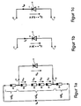
- Solar modules are well known and exist according to Fig. 1a usually from a series circuit of cells, which deliver a single voltage Uz of about 0.5 V to 1 V.
- Uz the voltage on the shaded cells reverses when loaded.
- the permissible reverse voltage of a solar cell is a few V up to a few 10 V.
- the permissible reverse voltage can be exceeded, resulting in local breakdown of the barrier layer and irreversible damage to the solar cell Cell can lead.
- To avoid this unacceptably high reverse voltage is known, ideally a so-called.
- Bypass diode to switch parallel to each cell. This effort is considerable and only in special applications, see eg space travel, portable.
- Fig. 1a Subgroups UG A , UG B , ... UG x formed by series-connected cells, eg 18 to 24, which are each protected by a bypass diode. These are connected via connection points 11, 12 with the respective subgroup. For the sake of clarity, is in FIG. 1a the bypass diode only for the subgroup UG B shown.
- the number of cells combined in a subgroup is selected so that in the worst case the permissible reverse voltage of the shaded single cell is not exceeded. This results in a typical number of about 18 to 24 cells per subgroup.
- the solar generator current I SG flows through the bypass diode and causes a voltage drop U D from about -0.4 V to more than -1 V.
- blocking voltage of +20 V and a forward voltage U D of -0.6 V where other values may occur.
- bypass diodes are usually housed in a junction box with the solar panel is exposed, and thus ambient temperatures of about -20 ° C to more than 85 ° C exposed. In one can, typically two or three diodes are accommodated for two or three subgroups UG A , UG B and UG C. To increase the permissible solar generator currents I SG and multiple bypass diodes can be connected in parallel.
- the invention is therefore based on the object to provide a protective switching device for a solar module, which performs the functions of a bypass diode, which provides little power loss and is simple in construction, and ensures a large and long reliability.
- a controllable electrical serving as a bypass element switching element
- the switching path parallel to the plurality of solar cells is connectable and that a supply circuit provides a control voltage for driving the control electrode
- a bypass circuit is provided, which can take over without difficulty the short-circuit or operating point current of the shaded solar cells.
- the controllable bypass element is controlled in its function so that little power loss occurs.
- the isolating circuit which is furthermore provided, the voltage lying in normal operation of the solar cells over the switching path of the switching element can be blocked to the supply circuit, while in the case of shading the isolating circuit switches the voltage lying across the switching path to the supply circuit.
- the supply circuit is designed as a charging circuit for an energy storage or has such that makes a boosting a voltage available in the event of shading in a higher voltage for driving the controllable bypass element.
- the supply voltage of -0.6 V available via the switching path in the event of shading can be used in order to control the controllable bypass element and possibly to supply further circuits.
- controllable bypass element is designed as a MOS field-effect transistor (MOSFET), wherein the inherent in the MOSFET body diode for a short time the solar generator current can take over completely and can be used permanently as a bypass diode for small solar generator currents.
- MOSFET MOS field-effect transistor
- controllable bypass element capacitance in the MOSFET used, the gate capacitance, used as energy storage of the supply circuit or charging circuit, so that no additional memory components are necessary.
- the isolation circuit is designed as an inversely operated bipolar transistor, since it is conventionally operated in collector mode during normal operation and thus can easily block the occurring in normal operation positive drain-source voltage of 20 V.
- the isolation circuit is advantageous to form as a field effect transistor, preferably as a self-conducting J-FET, since this has a low on-resistance, so that the subsequent circuit is almost lossless connected to the voltage of the switching path of the bypass element, the drain-source voltage of the MOSFET.
- the supply circuit and / or charging circuit has a transformer with a positive feedback winding and a first electronic switching element, wherein the switching element and the transformer perform a tilting operation similar to a blocking oscillator, in which the energy stored in the transformer is stored in the energy store, eg the gate capacitance. is transmitted.
- a blocking oscillator in which the energy stored in the transformer is stored in the energy store, eg the gate capacitance. is transmitted.
- the first electronic switching element is inversely connected, so that it simultaneously forms the separation circuit and no additional components for the separation are necessary.
- the first discharge circuit is a non-linear-acting active discharge circuit which is high-impedance above a threshold voltage and below the threshold voltage, the threshold voltage being determined by the required for the complete control of the bypass switching element voltage of its control electrode. As a result, the accumulated power loss within the MOSFET can be further reduced.
- the first discharge circuit with a self-conducting J-FET, which in normal operation connects the control electrode of the bypass switching element to a reference potential and thus an undesired switching on of the Bypass switching element prevents, and forms in Abschattungsfall together with a network of diode, capacitor and discharge resistor is a timer, which periodically shuts off the bypass switching element after a defined time.
- a network of diode, capacitor and discharge resistor is a timer, which periodically shuts off the bypass switching element after a defined time.
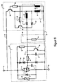
- protective switching device has as an essential part of a MOS field effect transistor 1, which is part of a switch unit 30, which will be described later in more detail.
- the drain-source path as a switching path is between the terminals 11 and 12, which are connected to the series connection of the solar cells of the solar module. In normal operation, a positive voltage of 20 V is present at the drain-source path, while in the case of shading a negative drain-source voltage of 0.6 V is present.
- the inherent body diode of the MOSFET 1 is denoted by 2.
- An isolating circuit 40 is connected, on the one hand, to the drain terminal of the MOSFET 1 and, on the other hand, to a supply and / or charging circuit 50 (hereinafter essentially referred to as a charging circuit), the isolating circuit 40, in normal operation, having the positive drain-source voltage of up to approx. 20 V, while in the event of shading it must forward the small negative voltage drop of 0.6 V or less to the subsequent charging circuit 50 with as little loss as possible.
- the charging circuit 50 converts the low negative direct voltage available in the shading case behind the isolating circuit 40 into a higher positive voltage required for driving the MOSFET 1 and / or for supplying further circuit parts.
- Concepts based on intermediate storage of energy in a choke coil or transformer and capacitive charge pumps may be used, with a preferred embodiment described later.
- the converted voltage is intermediately stored in an energy store 60, which is drawn here as a capacitor, wherein in a particularly advantageous manner, the gate capacitance of the MOSFET 1 is used directly as energy storage.
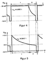
- the gate electrode G of the MOSFET 1 is controlled by a timer circuit 80 time-dependent, wherein the MOSFET is turned on for the most part of the cycle time to reduce the power loss, if necessary operates linearly over a shorter period and is completely blocked over a short period.
- the bypass current of the MOSFET 1 then flows through the body diode 2.
- the protective circuits according to FIGS. 3 . 6 and 7 is according to Fig. 5 in the first two time ranges discharges the gate capacitance of the MOSFET, while it is charged via the charging circuit at the end of the third time range.
- the discharge takes place according to Fig. 9 only in the time ranges 2 and 3, at the end of the fourth time range, the capacity is recharged via the charging circuit.
- a comparator 70 which monitors the drain-source voltage and in the allowable state gives a signal to a logic circuit 90, which also receives the signal from the timer circuit. Monitoring criteria of the comparator circuit 70, for example, the polarity and the height of the drain-source voltage of the MOSFET 1.
- a driver circuit 100 which is like all other circuits connected to the supply or charging circuit 50, controls the gate of the MOSFET 1 depending on the signal Logic circuit.
- FIG. 3 a first embodiment of the protection switching device according to the invention is shown with discrete components, wherein partially the function blocks are shown in dashed lines.
- the switch unit 30 has the MOSFET 1 with the body diode 2 as well as the inherently existing gate capacitance 3.
- a first zener diode 7 is connected in the forward direction to the gate terminal by the reference potential line connected to the terminal 12. It serves to limit the gate voltage to a permissible value of, for example, 15 V.
- a transistor 9 is connected with its switching path whose base is connected via a high-resistance resistor 10 to the drain terminal of the MOSFET 1 is.
- a further diode 4 may be connected, which conducts a part of or even the entire bypass current when the MOSFET 1 is not switched on.
- An overvoltage protection element 5, e.g. a varistor or TransZorb diode is connected in parallel with MOSFET 1 and limits extremely high short-time voltage pulses.
- the MOSFET with the body diode 2 inherently present is protected from excessive voltages at the drain-source path and the gate-source path.
- a quick shutdown required and continue to prevent unintentional switching of the MOSFET in normal operation.
- the transistor 9 At a positive drain-source voltage, ie the transition to normal operation, the transistor 9 is completely controlled by the high-impedance base resistor 10 and discharges the gate capacitance 3 of the MOSFET 1 via the low-impedance resistor 6 very fast (positive feedback). Furthermore, the transistor 9 keeps the gate-source voltage across the series resistor 6 in normal operation to almost 0 V. Thus, an unwanted switching, for example, by a gate voltage induced from the outside, reliably prevented. The effluent in normal operation on the base resistor 10 leakage current is negligible with appropriate dimensioning.
- MOSFETs are limited in avalanche-tight, i. if the maximum permissible drain-source voltage is briefly exceeded, e.g. greater than 60V, with a MOSFET specified for 40V, the MOSFET becomes conductive and limits the voltage spike without damage. In this mode of operation, however, the permissible working range can be left and the component can be subject to increased stress. Therefore, the MOSFET is selectively driven via its gate-source path via the zener diode 14 and the diode 13 when an excessive voltage occurs, the gate being raised to a positive potential when the zener voltage of the zener diode 14 is exceeded, and the MOSFET 1 in the linear range is operated. In order to be able to build up a positive gate voltage when the transistor 9 is conductive, the series resistor 6 is required.
- the capacitor is advantageously connected to the side facing away from the gate side of the series resistor 6, since then in the case of a transient overvoltage only the comparatively low gate capacitance 3 via the Zener diode 14 and the diode 13 must be loaded.
- the separation circuit 40 has the task to separate the normal operation positive drain-source voltage of 20 V from the subsequent circuit and the case of Abschattungsfall negative drain-source voltage of 0.6 V with low loss to the subsequent circuit parts forward.
- isolation circuit 40 has a N-channel self-conducting junction FET (J-FET) 28 whose source is connected to the drain terminal of the MOSFET 1 whose drain is connected to the subsequent supply or charging circuit 50 and the gate electrode via a high-resistance gate resistor 29 is connected to the reference potential line 32.
- This resistor 29 limits the current through the gate diodes at a positive gate-drain or gate-source voltage greater than 0.5 V, as occurs in Abschattungsfall.
- the low-resistance J-FET 28 requires a gate voltage of approximately 5 V, which is negative with respect to both drain and source. This is achieved directly in normal operation for the source-gate path. For the drain-gate path, however, this can only be achieved if the drain potential assumes a positive value. For this purpose, it is necessary that the subsequent supply or charging circuit 50 can receive a blocking voltage in the amount of the threshold voltage of the J-FET, ie about 5 V. This special property is ensured by the charging circuit 50 described below.
- a self-conducting MOSFET can be used, which have a similar behavior, but then a current limiting across the resistor 29 is not necessary, since the gate insulation can typically accommodate ⁇ 20V.
- the supply and / or charging circuit 50 has the task of converting a negative input voltage of 0.6 V into a sufficient for driving the MOSFET 1 positive output voltage of 15 V, for example. Taking into account the decreasing with increasing temperature voltage drop across the body diode 2 of the MOSFET 1 and possibly occurring voltage drops in the isolation circuit 40, a safe start must be ensured even at voltages of less than 0.4 V. Furthermore, the charging circuit must be very robust and with minimal effort to create. It additionally takes over the functions of the comparator 70 as well as partially of the time and driver circuits 80, 100 FIG. 2 ,
- the charging circuit 50 has a common-emitter transistor 24 whose emitter is connected to the drain terminal of the J-FET 28 and whose collector is connected to the primary winding 21 of a converter transformer 20.
- the base of the transistor 24 is connected via a series resistor 25 to a positive feedback winding 22.
- In series with the primary winding 21 is an output winding 21 ', whereby the converter transformer 20 is connected as an autotransformer.
- the collector of transistor 24 is connected between primary winding 21 and output winding 21 '.
- the output winding 21 ' is connected via a rectifier diode 23 and the series resistor 6 to the gate capacitance 3 or directly to the additional capacitor 8. Another diode 23 'connects the end of the primary winding to the additional capacitor 8.
- the charging circuit 50 has a transistor 26 whose emitter is connected to the drain terminal of the J-FET 28, whose collector between the diode 3 and the series resistor 6 and its base via a series resistor 27 to the terminal of the positive feedback winding 22.
- a discharge resistor 81 which may be part of a timer circuit 80 ', is between reference potential line 32 and gate control line 31 connected.
- the MOSFET 1 loaded on eg 15V. If the threshold voltage of the MOSFET 1 is reached at, for example, 5 V gate-source voltage, this goes from fully driven to linear region (region (2)), and the drain-source voltage increases accordingly FIG. 4 slowly. Without the recharging of the gate-source capacitance 3 described below via the charging circuit 50, the MOSFET 1 would go into the completely blocked state, in which case the solar generator current flows completely through the body diode 2, connected to a negative voltage drop of approx 0.4 V up to about 1 V.
- a sufficiently large base current flows in the transistor 24 to cause a significant collector current and thus current through the primary winding 21 of the transformer 20.
- a voltage is induced in the positive feedback winding 22, which adds due to the sense of winding to the voltage between the lines 32 and 34 and thus amplifies the base current, whereby a tilting operation begins.
- the transistor 24 is completely turned on and it builds up according to the inductance of the primary winding 21 and the applied voltage across the primary winding, which substantially corresponds to the voltage applied between the lines 32, 34, a time-increasing primary current.
- the core of the transformer 20 saturates, or if the base current of the transistor 24 is no longer sufficient for complete control, the positive feedback is reversed and the transistor 24 is abruptly blocked.
- the stored energy in the transformer inductance is transmitted through the primary winding 21 and the output winding 21 'and the rectifier diode 23 in the gate capacitance 3 and the additional capacitor 8. This is at the end of the range (3) or at the beginning of the range (1) of the FIGS. 4 and 5 to recognize.
- the MOSFET 1 thus turns on and has, as described, according to its internal resistance only a negative voltage drop of a few millivolts.
- the charging circuit 50 is then not sufficiently powered and is not active.
- the transformer 20 is dimensioned so that the energy stored in it is sufficient to charge the gate capacitance 3 or the capacitor 8 to the desired value of, for example, 15 V already with a converter clock cycle.
- the unavoidable stray inductance of the transformer winding 21 during rapid turn-off of the transistor 24 leads to an overvoltage peak on the transistor 24, which can damage it. Diode 23 'prevents this spike by allowing the current flowing in the transformer winding at the moment of turn-off to flow into the then-uncharged capacitor.
- clock always refers to the charging circuit 50
- cycle always refers to the overall circuit.
- the charge cycle consists of two phases: The first phase has been described above and it starts and extends over the duration of the range (3) of the total cycle. The tilting process itself only takes a few ⁇ s, the essential part of the time consists in the "slow” rise of the current to the end of the range (3). Then the second clock phase sets in, in which the energy is transferred from the transformer to the capacitors. This process is on the falling edge, ie partially in the range (3) and in the range (1) of the subsequent cycle. But this reloading process takes a total of only a few ⁇ s.
- the transistor 24 with its base-emitter path assumes not only the switching function but also the function of the comparator 70 FIG. 2 ie it only works if the applied drain-source voltage is high enough.
- the transistor 24 is therefore thermally coupled to the MOSFET 1. Since both components are based on silicon technology, the forward voltages of the body diode and also of the base-emitter diode change in the same direction, so that a safe function of the circuit is guaranteed at all temperatures.
- the tilting process or transducer cycle described above which is given by the area (3), not necessarily completely.
- the gate capacitance 3 of the MOSFET 1 or the capacitor 8 can not be fully charged, in particular in the case of small solar generator currents.
- the gate of the MOSFET 1 is discharged very quickly via the then turned-on transistor 26 when the tilting process starts, as is apparent FIG. 5 , Area (3) can be seen.
- the MOSFET 1 is momentarily blocking and the drain-source voltage is increasing accordingly Fig. 4 fast from approx. -0.4 V to the threshold value of the tilting process, to approx. -0.6 V, the forward voltage of the body diode 2.
- the transistor 26 thus creates an additional positive feedback.
- the transistor 26 is completely blocked by the then negative voltage at the positive feedback winding 22, so that the gate capacitor 3 and the capacitor 8 can be charged.
- FIGS. 4 and 5 The overall cycle of the circuit after FIG. 3 sits down accordingly FIGS. 4 and 5 from a first, long phase (100 ms) together, in which the MOSFET 1 is completely turned on, a second, shorter phase (20 ms), in which it enters the linear region and the drain-source voltage slowly increases to about -0.4 V and a third, short phase in which it is completely switched off by the positive feedback circuit for a short time (eg 1 ms).
- a short time eg 1 ms
- the drain-source voltage of the MOSFET increases to positive values of approx. 15 V to approx. 20 V.
- both its drain and its source must be positive by about 5 V with respect to the gate, otherwise an unallowable leakage current would flow into the charging circuit 50.
- the emitter bases of the positive voltage transistors 24 and 26 on the line 34 are reverse biased and they can also accept a reverse voltage of up to about 5V, the drain potential of the J-FET 28 may rise to 5V and the J-FET 28 with it, as required, completely lock.
- FIG. 6 is shown a further embodiment, which simplifies the in FIG. 3 shown circuit achieved in that the functions of the separation circuit 40 and the transistor 24 of the supply or charging circuit 50 are summarized. Otherwise, the circuit corresponds to the after FIG. 3 and also the voltage diagrams after FIG. 4 and FIG. 5 are applicable.
- the transistor 24 is operated inversely. If the emitter and the collector are swapped in a bipolar transistor, the basic principle remains Transistor properties obtained in reverse operation, however, the current gain decreases by about a factor of 30. This property is met with a correspondingly low-impedance base series resistor 25. In practice, the ohmic resistance of the positive feedback winding 22 may already be sufficient for limiting the current, so that no concentrated component 25 has to be used.
- the inverse operation of the transistor 24 has the great advantage that it is operated in collector mode during normal operation of the solar module, its base and also the emitter lying DC voltage on the reference potential 32.
- the transistor can easily pick up the 20V voltage that occurs, and it is also possible to use a voltage-proof type of transistor that better resists any overvoltage pulses.
- An oscillation of the supply or charging circuit is excluded because of the negative feedback winding 22 acting as negative feedback in this operating case.
- the transistor 26 continues to be operated conventionally and its function corresponds to that in FIG Fig. 3 , Its emitter, however, is connected to the emitter of the transistor 24.
- the gate of the MOSFET 1 can be discharged quickly via transistor 26, wherein it does not have to absorb negative reverse voltages in this type of interconnection in the Leitendphase of the MOSFET 1 and in normal operation of the module.
- the necessary energy to charge the gate capacitance 3 and the capacitor 8 in a single cycle ie in a single tilting operation of the converter transformer 20 and the transistor 24.
- the charging circuit can also transfer the energy in several cycles, where it charges the gate capacitance of the MOSFET 1 or an energy store in several cycles and then switches off.
- the already mentioned incomplete charging of the gate capacitance or of the capacitor 8 can also be achieved by an appropriate dimensioning, e.g. of the basic series resistor 25, are raised to the principle in order to achieve the permanently linear region of the MOSFET 1.
- the transistor 24 serves as a regulator for the drain-source voltage.
- the MOSFET 1 is not completely controlled in this case, but held over the transistor 24 as a regulator in linear operation.
- a negative voltage of approximately 0.3 V to 0.4 V drops across the drain-source path, which is sufficient to allow the supply or charging circuit 50 to run continuously.
- the losses within the MOSFET 1 are greater than with a fully switched MOSFET.
- the advantage, however, is that no jumps occur in the solar generator voltage or the solar generator current in this linearly operating MOSFET.
- FIG. 7 shows a circuit differing from the circuit FIG. 3 respectively.
- FIG. 6 by the discharge circuit designated 80 " FIG. 3 and FIG. 6 becomes the shutdown time of the MOSFET 1 is determined by the timer formed by its gate capacitance 3, the optional capacitor 8 and the discharge resistor 81.
- a non-linear active, active gate discharge circuit is used. This has the property that it is high-impedance above a certain threshold voltage, but falls significantly lower impedance when falling below the threshold voltage.
- a circuit with this property can be realized for example by a Schmitt trigger circuit. If the switching point of this trigger circuit, ie the flip-flop of the gate discharge circuit 80 "is set higher than the highest required for complete control of the MOSFET 1 gate voltage, for example to 6 V or greater, so this is after a charge through the Charging circuit 50 initially drop slowly to rapidly fall below the trigger or overturning threshold and trigger a new charging clock With such a circuit, the operation of the MOSFET 1 in the linear range, the in FIG. 4 and FIG. 5 With area (2) is called, avoided and lowered the power loss again.
- a small-signal MOSFET 87 is connected between gate control line 31 and reference potential line 32, whose gate terminal is connected to the collector of a transistor 83 whose emitter is in turn at the reference potential 32.
- the base terminal is connected to a voltage divider 84 85 is connected between gate control line 31 and reference potential line 32.
- a resistor 86 is connected between line 31 and gate terminal of MOSFET 87.
- a capacitor 88 is connected to the positive feedback winding 22.
- the transistor 83 through the voltage divider 84, 85 completely controlled. Its collector potential and thus also the gate potential of the MOSFET 87 are therefore close to the reference potential 32 and the MOSFET 87 is thus blocked.
- the gate capacitance 3 of the MOSFET 1 and the capacitor 8 are slowly discharged via the high-resistance resistors 84, 85 and 86. If the gate voltage from the MOSFET 1 drops below a minimum value, transistor 83 begins to block and the gate voltage of the MOSFET 87 rises. If its threshold voltage is e.g. reaches about 1 ... 2 V in a small-signal MOSFET 87, so its drain-source path is low-resistance and the gate capacitance 3 and the capacitor 8 are discharged quickly. As a result, the base current for the transistor 83 further decreases and it starts a tilting operation.
- the MOSFET 87 is completely blocked by means of the negative voltage jump at the positive feedback winding 22 transmitted by the capacitor 88, so that the gate capacitor 3 or the capacitor 8 can be charged again.
- FIG. 8 shows a further, particularly advantageous embodiment of the protection circuit. It essentially corresponds to the circuit Fig. 6 , wherein the transistor is omitted together with series resistor 10 and the passive discharge circuit 80 'by an active discharge circuit 80''' has been replaced.
- the core of the active discharge circuit 80 ''' is the normally-on J-FET 81'. It replaces the transistor 9 together with the series resistor 10 by connecting the gate of the MOSFET 1 via the series resistor 6 and the windings 21 'and 21 of the transformer to the reference potential conductor 32 in the normal operation of the solar module.
- unwanted switching of the MOSFET 1 is reliably prevented by externally induced gate voltages or leakage currents of the diodes 13 and 14.
- it allows optimal control of the MOSFET 1 according to Fig. 9 , which leads to a further reduction of the power loss in the bypass switching element.
- the circuit is after Fig. 8 the gate of the MOSFET 1 after the charging process is not discharged by a resistor, but the gate voltage U GS keeps according to Fig. 9 during the entire period 1 its full value. As a result, the MOSFET is very low in this time, and the power loss is correspondingly low.
- the shutdown time of the MOSFET 1 is determined by a time constant of the timer formed by capacitor 82 'and resistor 84'. In the charging phase of the capacitors 8 and 3 at the end of the period 4, the capacitor 82 'is also charged via the diode 83' to the sum of the voltages across the three windings 21, 21 'and 22, in this example to 17.5 V.
- the potential at the gate of the J-FET 81' jumps to a value of -17.5 V.
- the J-FET is thus completely blocked, and, ideally, no charge can flow away from the capacitors 8 and 3.
- the resistor 84 ' the capacitor 82' is discharged slowly, eg within 100 ms.
- the gate voltage of the J-FET 81 ' reaches its threshold voltage (2V in this example)
- the J-FET becomes low-resistance and discharges the capacitors 8 and 3 via the windings 21' and 21, thereby increasing the gate voltage U GS of the MOSFET 1 drops very fast, resulting in Fig.
- circuits can all be constructed with complementary semiconductor types.
- the MOSFET 1 as an additional function can also take over a short circuit of the solar generator voltage during installation, in the event of an inspection or in case of fire.
- the gate terminals of all MOSFETs within a solar generator with a control voltage applied so that the voltage of each individual module is short-circuited.
- Protective switching device for a solar module in which a plurality of partly working in normal operation and at the same time partly in Abschattungsfall solar cells are connected in series, with at least one controllable electrical, serving as a bypass element switching element, the switching path is connected parallel to the plurality of solar cells with a supply circuit 50 for providing a control voltage for driving the control electrode of the bypass element 1 and with an isolating circuit 40 for blocking the voltage across the switching path of the bypass element in normal operation to the supply circuit 50 and for switching through the voltage over the switching path in the case of parasitic case of at least one solar cell voltage to the supply circuit 50th
- the supply circuit is designed as a charging circuit 50 for an energy store 3, 8, 60, which carries out a conversion of the voltage available in the shading case into a voltage which is higher for driving the controllable bypass element.
- the controllable bypass element 1 is designed as a MOS field effect transistor.
- the energy store is designed as a capacitor 8 and / or as the controllable bypass element (1) inherent capacity 3.
- the isolation circuit 40 is designed as a field effect transistor, preferably as a J-FET or as a MOSFET.
- the isolation circuit is designed as an inversely operated bipolar transistor.
- a timer circuit 80 is provided, which predetermines a time cycle during which the controllable bypass element 1 is completely switched through over a first time range and a second time range is completely blocked, the energy store 3, 8, 60 being charged in the second time range.
- the time cycle has a third time range lying between the first and the second time range, in which the controllable bypass element 1 is operated in the linear state.
- the supply or charging circuit 50 has a control circuit 24, with which the controllable bypass element is constantly operable in the linear state.
- the supply or charging circuit 50 has to generate the voltage required for the control of the controllable bypass element 1 to a transformer or at least one coil or at least one capacitor for temporary storage of energy for the increase in the voltage available in the case of shading.
- the supply or charging circuit 50 has to generate the voltage required for the control of the controllable bypass element 1, a charge pump for increasing the voltage available in the case of shading on.
- the supply circuit 50 has a transformer 20 with a positive feedback winding 22 and a first electronic switching element 24, wherein switching element and transformer 20 similar to a blocking oscillator perform a tilting operation in which the stored energy in the transformer 20 in the energy storage 3, 8, 60 is transmitted.
- the first electronic switching element 24 is operated inversely and simultaneously forms the separating circuit 40.
- An additional output winding 21 'similar to an autotransformer is connected in series with the primary winding 21.
- the switching path of the first switching element 24 is connected to the primary winding 21 in series and the positive feedback winding 22 is connected to the control electrode of the first switching element 24.
- the control electrode of the controllable bypass element 1 is connected to a first discharge circuit 80 ', 80' ', 80' '', wherein the time constant of the first discharge circuit is selected such that the ratio of the time of conducting the bypass element 1 to the non-conducting is large, preferably> 5.
- the first discharge circuit has a resistor 81 connected in parallel to the inherent capacitance 3 of the bypass element 1 and optionally to a capacitor 8 connected in parallel with it.
- the supply circuit 50 has a fast discharge circuit 26, which quickly discharges the inherent capacitance 3 and possibly the auxiliary capacitor 8 connected in parallel at the onset of the tilting process.
- the quick discharge circuit has a second electronic switching element 26, whose control electrode is connected to the positive feedback winding and whose switching path, starting from the terminal of the control electrode of the bypass switching element 1 is parallel to the switching path of the first electronic switching element 24 or in series therewith.
- the first discharge circuit 80 is designed as a non-linear active discharge circuit, which is high-impedance above a threshold voltage and low below the threshold voltage, the threshold voltage is determined by the voltage required for the complete control of the bypass switching element 1 at its control electrode.
- the first discharge circuit 80 is designed as a Schmitt trigger circuit.
- the first discharge circuit 80 ''' has a normally-on J-FET and a network of diode 83', capacitor 82 'and discharge resistor 83', which form a timer for periodically switching off the bypass switching element after a defined time.
- the controllable bypass switching element is assigned a protection circuit 30 against overvoltage and against unwanted switching.
- control electrodes of the bypass elements is set to such a voltage that the bypass elements are turned on.
Abstract
Description
Die Erfindung betrifft eine Schutzschalteinrichtung für ein Solarmodul, bei dem eine Mehrzahl von Solarzellen in Reihe geschaltet ist.The invention relates to a protective switching device for a solar module, in which a plurality of solar cells is connected in series.
Solarmodule sind allgemein bekannt und bestehen gemäß
Im Folgenden wird unabhängig von der tatsächlichen Ursache der Spannungsumkehr immer der Begriff "Abschattungsfall" benutzt, für den nicht abgeschatteten Betrieb der Begriff "Normalbetrieb".In the following, regardless of the actual cause of the voltage reversal, the term "shading case" is always used, for the non-shaded operation the term "normal operation" is used.
Die zulässige Sperrspannung einer Solarzelle liegt bei einigen wenigen V bis zu einigen wenigen 10 V. Abhängig von der Anzahl der mit der abgeschatteten Zelle in Reihe geschalteten, nicht abgeschatteten Zellen kann die zulässige Sperrspannung überschritten werden, was zu lokalen Durchbrüchen der Sperrschicht und irreversiblen Schädigungen der Zelle führen kann. Zur Vermeidung dieser unzulässig hohen Sperrspannung ist bekannt, idealerweise eine sog. Bypassdiode parallel zu jeder einzelnen Zelle zu schalten. Dieser Aufwand ist erheblich und nur bei Sonderanwendungen, siehe z.B. die Raumfahrt, tragbar. In handelsüblichen Solarmodulen werden daher gemäß
Im Normalbetrieb liegt gemäß
Die Anzahl der in einer Untergruppe zusammengefassten Zellen wird so gewählt, dass im schlimmsten Fall die zulässige Sperrspannung der abgeschatteten Einzelzelle nicht überschritten wird. Dies führt zu einer typischen Anzahl von ca. 18 bis zu 24 Zellen pro Untergruppe.The number of cells combined in a subgroup is selected so that in the worst case the permissible reverse voltage of the shaded single cell is not exceeded. This results in a typical number of about 18 to 24 cells per subgroup.
Für die bekannte Bypassdiode ergeben sich somit folgende Betriebsbedingungen:The following operating conditions thus result for the known bypass diode:
In dem in
Die Bypassdioden sind üblicherweise in einer Anschlussdose untergebracht, die mit dem Solarmodul verbunden ist, und somit Umgebungstemperaturen von ca. -20 °C bis zu mehr als 85 °C ausgesetzt. In einer Dose sind typischerweise zwei oder drei Dioden untergebracht für zwei oder drei Untergruppen UGA, UGB und UGC. Zur Erhöhung der zulässigen Solargeneratorströme ISG können auch mehrere Bypassdioden parallel geschaltet sein.The bypass diodes are usually housed in a junction box with the solar panel is exposed, and thus ambient temperatures of about -20 ° C to more than 85 ° C exposed. In one can, typically two or three diodes are accommodated for two or three subgroups UG A , UG B and UG C. To increase the permissible solar generator currents I SG and multiple bypass diodes can be connected in parallel.
In den im Stand der Technik eingesetzten Bypassdioden entsteht im Falle einer Abschattung eine relativ große Verlustleistung. Eine solche Verlustleistung kann kurzfristig problemlos von der Diode aufgenommen werden, bei länger andauernden Abschattungen ist es jedoch schwierig, die entstehende Wärmemenge von der Diode und aus der Anschlussdose abzuführen. Dabei ist zusätzlich der Umstand zu berücksichtigen, dass die höchsten Belastungen, d.h. die höchsten Solarströme zumeist bei gleichzeitig hohen Umgebungs- bzw. Modultemperaturen auftreten. Das Problem verschärft sich mit größer werdenden Solarzellen, da diese einen proportional zur Zellfläche ansteigenden Kurzschluss- bzw. Nennstrom liefern.In the bypass diodes used in the prior art, a relatively large power loss occurs in the case of shading. Such a power loss can be easily absorbed by the diode in the short term, but with longer-lasting shadowing, it is difficult to dissipate the heat generated from the diode and the junction box. In addition, the fact that the highest loads, i. The highest solar currents usually occur at the same time high ambient or module temperatures. The problem is worsening with increasing solar cells, as these provide a proportional to the cell surface increasing short-circuit or rated current.
Der Erfindung liegt daher die Aufgabe zugrunde, eine Schutzschalteinrichtung für ein Solarmodul zu schaffen, die die Funktionen einer Bypassdiode übernimmt, wobei sie wenig Verlustleistung liefert und einfach aufgebaut ist, und eine große und lange Zuverlässigkeit gewährleistet.The invention is therefore based on the object to provide a protective switching device for a solar module, which performs the functions of a bypass diode, which provides little power loss and is simple in construction, and ensures a large and long reliability.
Diese Aufgabe wird erfindungsgemäß durch die Merkmale des Hauptanspruchs gelöst.This object is achieved by the features of the main claim.
Dadurch, dass ein steuerbares elektrisches, als Bypasselement dienendes Schaltelement vorgesehen ist, dessen Schaltstrecke parallel zu der Mehrzahl von Solarzellen anschließbar ist und dass eine Versorgungsschaltung eine Steuerspannung zur Ansteuerung der Steuerelektrode bereitstellt, wird eine Bypassschaltung zur Verfügung gestellt, die ohne Schwierigkeit den Kurzschluss- oder Arbeitspunktstrom der abgeschatteten Solarzellen übernehmen kann. Mittels der Versorgungsspannung wird das steuerbare Bypasselement in seiner Funktion so gesteuert, dass wenig Verlustleistung auftritt. Durch die weiterhin vorgesehene Trennschaltung kann die im Normalbetrieb der Solarzellen über der Schaltstrecke des Schaltelementes liegende Spannung zu der Versorgungsschaltung gesperrt werden, während im Abschattungsfall die Trennschaltung die über der Schaltstrecke liegende Spannung zu der Versorgungsschaltung durchschaltet.Characterized in that a controllable electrical, serving as a bypass element switching element is provided, the switching path parallel to the plurality of solar cells is connectable and that a supply circuit provides a control voltage for driving the control electrode, a bypass circuit is provided, which can take over without difficulty the short-circuit or operating point current of the shaded solar cells. By means of the supply voltage, the controllable bypass element is controlled in its function so that little power loss occurs. As a result of the isolating circuit which is furthermore provided, the voltage lying in normal operation of the solar cells over the switching path of the switching element can be blocked to the supply circuit, while in the case of shading the isolating circuit switches the voltage lying across the switching path to the supply circuit.
Durch die in den Unteransprüchen angegebenen Maßnahmen sind vorteilhafte Weiterbildungen und Verbesserungen möglich.The measures specified in the dependent claims advantageous refinements and improvements are possible.
Besonders vorteilhaft ist, dass die Versorgungsschaltung als Ladeschaltung für einen Energiespeicher ausgebildet ist oder eine solche aufweist, die eine Hochsetzung einer im Abschattungsfall zur Verfügung stehenden Spannung in eine zur Ansteuerung des steuerbaren Bypasselementes höhere Spannung vornimmt. Auf diese Weise kann die über die Schaltstrecke im Abschattungsfall zur Verfügung stehende Versorgungsspannung von -0,6 V verwendet werden, um das steuerbare Bypasselement anzusteuern und ggf. weitere Schaltungen zu versorgen.It is particularly advantageous that the supply circuit is designed as a charging circuit for an energy storage or has such that makes a boosting a voltage available in the event of shading in a higher voltage for driving the controllable bypass element. In this way, the supply voltage of -0.6 V available via the switching path in the event of shading can be used in order to control the controllable bypass element and possibly to supply further circuits.
In vorteilhafter Weise ist das steuerbare Bypasselement als MOS-Feldeffekttransistor (MOSFET) ausgebildet, wobei die in dem MOSFET inhärent vorhandene Body-Diode kurzzeitig den Solargeneratorstrom vollständig übernehmen kann und bei kleinen Solargeneratorströmen dauerhaft als Bypassdiode genutzt werden kann.Advantageously, the controllable bypass element is designed as a MOS field-effect transistor (MOSFET), wherein the inherent in the MOSFET body diode for a short time the solar generator current can take over completely and can be used permanently as a bypass diode for small solar generator currents.
In vorteilhafter Weise wird die dem steuerbaren Bypasselement inhärente Kapazität, bei dem verwendeten MOSFET die Gate-Kapazität, als Energiespeicher der Versorgungsschaltung bzw. Ladeschaltung verwendet, so dass keine zusätzlichen Speicher-Bauelemente notwendig sind.Advantageously, the inherent to the controllable bypass element capacitance, in the MOSFET used, the gate capacitance, used as energy storage of the supply circuit or charging circuit, so that no additional memory components are necessary.
In besonders vorteilhafter Weise ist die Trennschaltung als invers betriebener Bipolar-Transistor ausgebildet, da dieser im Normalbetrieb konventionell in Kollektorschaltung betrieben wird und somit die im Normalbetrieb auftretende positive Drain-Source-Spannung von 20 V problemlos sperren kann.In a particularly advantageous manner, the isolation circuit is designed as an inversely operated bipolar transistor, since it is conventionally operated in collector mode during normal operation and thus can easily block the occurring in normal operation positive drain-source voltage of 20 V.
Vorteilhaft ist, die Trennschaltung als Feldeffekttransistor, vorzugsweise als selbst leitenden J-FET auszubilden, da dieser einen geringen Einschaltwiderstand aufweist, so dass die nachfolgende Schaltung nahezu verlustfrei mit der Spannung der Schaltstrecke des Bypasselementes, der Drain-Source-Spannung des MOSFET verbunden ist.It is advantageous to form the isolation circuit as a field effect transistor, preferably as a self-conducting J-FET, since this has a low on-resistance, so that the subsequent circuit is almost lossless connected to the voltage of the switching path of the bypass element, the drain-source voltage of the MOSFET.
In vorteilhafter Weise weist die Versorgungsschaltung und/oder Ladeschaltung einen Transformator mit einer Mitkopplungswicklung und ein erstes elektronisches Schaltelement auf, wobei Schaltelement und Transformator ähnlich einem Sperrschwinger einen Kippvorgang ausüben, bei dem die im Transformator gespeicherte Energie in den Energiespeicher, z.B. die Gate-Kapazität, übertragen wird. Durch diese Maßnahme ist es möglich, aus der geringen Spannung im Abschattungsfall von ca. 0,6 V eine hohe Spannung von etwa 15 V zu erzeugen, wobei die notwenige Energie zur Ladung der Gate-Kapazität schnell, vorzugsweise in einem einzigen Takt, übertragen werden kann.In an advantageous manner, the supply circuit and / or charging circuit has a transformer with a positive feedback winding and a first electronic switching element, wherein the switching element and the transformer perform a tilting operation similar to a blocking oscillator, in which the energy stored in the transformer is stored in the energy store, eg the gate capacitance. is transmitted. By this measure, it is possible from the low voltage in Abschattungsfall of about 0.6 V, a high voltage of about 15 V, wherein the necessary energy for charging the gate capacitance can be transmitted quickly, preferably in a single clock.
In besonders vorteilhafter Weise ist das erste elektronische Schaltelement invers geschaltet, so dass es gleichzeitig die Trennschaltung bildet und keine zusätzlichen Bauelemente für die Trennung notwendig sind.In a particularly advantageous manner, the first electronic switching element is inversely connected, so that it simultaneously forms the separation circuit and no additional components for the separation are necessary.
Durch Vorsehen einer ersten Entladeschaltung, die mit der Steuerelektrode des steuerbaren Bypasselementes verbunden ist, wobei die Zeitkonstante der Entladeschaltung so gewählt ist, dass das Verhältnis der Zeit des Leitens des Bypasselementes zu der des Nicht-Leitens groß ist, vorzugsweise größer als 5, ist es möglich, das steuerbare Bypasselement so zu steuern, dass geringe Verlustleistungen auftreten und somit die Wärmeentwicklung gering ist.By providing a first discharge circuit connected to the control electrode of the controllable bypass element, wherein the time constant of the discharge circuit is selected such that the ratio of the time of conducting the bypass element to that of non-conducting is large, preferably greater than 5, it is possible to control the controllable bypass element so that low power losses occur and thus the heat generation is low.
Vorteilhaft ist, die erste Entladungsschaltung als nicht linear wirkende aktive Entladungsschaltung auszubilden, die oberhalb einer Schwellenspannung hochohmig und unterhalb der Schwellenspannung niederohmig ist, wobei die Schwellenspannung durch die für die vollständige Durchsteuerung des Bypassschaltelementes benötigte Spannung seiner Steuerelektrode bestimmt ist. Dadurch kann die anfallende Verlustleistung innerhalb des MOSFET weiter verringert werden.It is advantageous to form the first discharge circuit as a non-linear-acting active discharge circuit which is high-impedance above a threshold voltage and below the threshold voltage, the threshold voltage being determined by the required for the complete control of the bypass switching element voltage of its control electrode. As a result, the accumulated power loss within the MOSFET can be further reduced.
Besonders vorteilhaft ist es, die erste Entladeschaltung mit einem selbstleitenden J-FET zu realisieren, der im Normalbetrieb die Steuerelektrode des Bypassschaltelementes mit einem Referenzpotenzial verbindet und so ein ungewolltes Einschalten des Bypassschalt-elementes verhindert, und der im Abschattungsfall zusammen mit einem Netzwerk aus Diode, Kondensator und Entladewiderstand ein Zeitglied bildet, welches das Bypassschaltelement periodisch nach einer definierten Zeit abschaltet. Hierdurch kann die Steuerelektrode des Bypassschaltelementes im durchgeschalteten Zustand immer auf einem optimalen Wert aufgeladen bleiben, wodurch sich die Verlustleistung weiter reduziert.It is particularly advantageous to realize the first discharge circuit with a self-conducting J-FET, which in normal operation connects the control electrode of the bypass switching element to a reference potential and thus an undesired switching on of the Bypass switching element prevents, and forms in Abschattungsfall together with a network of diode, capacitor and discharge resistor is a timer, which periodically shuts off the bypass switching element after a defined time. As a result, the control electrode of the bypass switching element in the switched-through state can always remain charged to an optimum value, as a result of which the power loss is further reduced.
Ausführungsbeispiele der Erfindung sind in der Zeichnung dargestellt und werden in der nachfolgenden Beschreibung näher erläutert. Es zeigen:
Figur 1- die Verschaltung von Solarzellen und Bypassdioden gemäß dem Stand der Technik sowie die Diodenspannung im Normalbetrieb und bei Abschattung,
Figur 2- ein Blockschaltbild der erfindungsgemäßen Schutzschalteinrichtung,
Figur 3- eine erste schaltungsgemäße Ausgestaltung der erfindungsgemäßen Schutzschalteinrichtung,
Figur 4- den zeitlichen Verlauf der Drain-Source-Spannung des steuerbaren Bypasselementes,
Figur 5- den zeitlichen Verlauf der Gate-Source-Spannung,
- Figur 6
- eine zweite schaltungsgemäße Ausgestaltung der erfindungsgemäßen Schalteinrichtung und
- Figur 7
- eine dritte schaltungsgemäße Ausgestaltung der erfindungsgemäßen Schutzschalteinrichtung,
- Figur 8
- eine vierte schaltungsgemäße Ausgestaltung der Erfindung und
- Figur 9
- den zeitlichen Verlauf der Gate-Source-Spannung des steuerbaren Bypasselementes und der Gate-Source-Spannung des selbstleitenden J-FET sowie den zeitlichen Verlauf der Drain-Source-Spannung des steuerbaren Bypasselementes.
- FIG. 1
- the interconnection of solar cells and bypass diodes according to the prior art and the diode voltage in normal operation and shading,
- FIG. 2
- a block diagram of the protective switching device according to the invention,
- FIG. 3
- a first circuit-specific embodiment of the protective switching device according to the invention,
- FIG. 4
- the time profile of the drain-source voltage of the controllable bypass element,
- FIG. 5
- the time course of the gate-source voltage,
- FIG. 6
- a second circuit-specific embodiment of the switching device according to the invention and
- FIG. 7
- a third circuit configuration the protective switching device according to the invention,
- FIG. 8
- a fourth circuit configuration of the invention and
- FIG. 9
- the time profile of the gate-source voltage of the controllable bypass element and the gate-source voltage of the normally-on J-FET and the time course of the drain-source voltage of the controllable bypass element.
Die in
Die Ladeschaltung 50 setzt die im Abschattungsfall hinter der Trennschaltung 40 zur Verfügung stehende geringe negative Gleichspannung in eine zur Ansteuerung des MOSFET 1 und/oder zur Versorgung weiterer Schaltungsteile erforderliche höhere positive Spannung um. Hierbei können Konzepte beruhend auf einer Zwischenspeicherung von Energie in einer Drosselspule oder einem Transformator sowie kapazitiv arbeitende Ladungspumpen zum Einsatz kommen, wobei eine bevorzugte Ausführungsform später beschrieben wird. Die gewandelte Spannung wird in einen Energiespeicher 60, der hier als Kondensator gezeichnet ist, zwischengespeichert, wobei in einer besonders vorteilhaften Weise die Gate-Kapazität des MOSFET 1 direkt als Energiespeicher genutzt wird.The charging
Die Gate-Elektrode G des MOSFET 1 wird mittels einer Zeitgeberschaltung 80 zeitabhängig angesteuert, wobei der MOSFET über den größten Teil der Zykluszeit zur Verringerung der Verlustleistung durchgesteuert ist, ggf. über einen geringeren Zeitraum linear arbeitet und über einen kurzen Zeitraum vollständig gesperrt ist. Der Bypass-Strom des MOSFET 1 fließt dann durch die Body-Diode 2. Bei den Schutzschaltungen gemäß
Vorzugsweise ist ein Komparator 70 vorgesehen, der die Drain-Source-Spannung überwacht und im zulässigen Zustand ein Signal an eine Logikschaltung 90 gibt, die gleichfalls das Signal der Zeitgeberschaltung erhält. Überwachungskriterien der Komparatorschaltung 70 sind beispielsweise die Polarität sowie die Höhe der Drain-Source-Spannung des MOSFET 1. Eine Treiberschaltung 100, die wie alle übrigen Schaltungen mit der Versorgungs- oder Ladungsschaltung 50 verbunden ist, steuert das Gate des MOSFET 1 abhängig vom Signal der Logikschaltung an.Preferably, a
Die in der
In
Parallel zur inhärent vorhandenen Body-Diode 2 des MOSFET 1 kann eine weitere Diode 4 geschaltet sein, die bei nicht eingeschaltetem MOSFET 1 einen Teil des oder auch den gesamten Bypass-Strom leitet.Parallel to the inherent existing
Ein Überspannungs-Schutzelement 5, z.B. ein Varistor oder eine TransZorb-Diode, liegt parallel zum MOSFET 1 und begrenzt extrem hohe, kurzzeitige Spannungsimpulse.An
Mit dieser Schutzschaltung wird der MOSFET mit der inhärent vorhandenen Body-Diode 2 vor zu hohen Spannungen an der Drain-Source-Strecke und der Gate-Source-Strecke geschützt. Außerdem ist beim Übergang in den Normalbetrieb, d.h. bei einer positiven Drain-Source-Spannung, ein schnelles Abschalten erforderlich und weiterhin soll ein ungewolltes Einschalten des MOSFET im Normalbetrieb verhindert werden.With this protection circuit, the MOSFET with the
Bei einer positiven Drain-Source-Spannung, d.h. beim Übergang zum Normalbetrieb, wird der Transistor 9 über den hochohmigen Basis-Vorwiderstand 10 vollständig durchgesteuert und entlädt die Gate-Kapazität 3 des MOSFET 1 über den niederohmigen Vorwiderstand 6 sehr schnell (Mitkopplung). Weiterhin hält der Transistor 9 die Gate-Source-Spannung über den Vorwiderstand 6 im Normalbetrieb auf nahezu 0 V. Damit wird ein ungewolltes Einschalten, z.B. durch eine von außen induzierte Gate-Spannung, zuverlässig verhindert. Der im Normalbetrieb über den Basis-Vorwiderstand 10 abfließende Verluststrom ist bei entsprechender Dimensionierung vernachlässigbar klein.At a positive drain-source voltage, ie the transition to normal operation, the transistor 9 is completely controlled by the high-
Grundsätzlich sind MOSFET begrenzt Avalanche-fest, d.h. bei kurzzeitiger Überschreitung der maximal zulässigen Drain-Source-Spannung, z.B. größer als 60 V, bei einem für 40 V spezifizierten MOSFET wird der MOSFET leitend und begrenzt die Spannungsspitze ohne Schaden zu nehmen. Bei dieser Betriebsart kann aber der zulässige Arbeitsbereich verlassen werden und das Bauteil einem verstärkten Stress unterliegen. Daher wird über die Zenerdiode 14 und die Diode 13 der MOSFET beim Auftreten einer überhöhten Spannung gezielt über seine Gate-Source-Strecke angesteuert, wobei beim Überschreiten der Zenerspannung der Zenerdiode 14 das Gate auf ein positives Potential angehoben wird und der MOSFET 1 im linearen Bereich betrieben wird. Um bei leitendem Transistor 9 eine positive Gate-Spannung aufbauen zu können, ist der Vorwiderstand 6 erforderlich.Basically, MOSFETs are limited in avalanche-tight, i. if the maximum permissible drain-source voltage is briefly exceeded, e.g. greater than 60V, with a MOSFET specified for 40V, the MOSFET becomes conductive and limits the voltage spike without damage. In this mode of operation, however, the permissible working range can be left and the component can be subject to increased stress. Therefore, the MOSFET is selectively driven via its gate-source path via the
Der über den Vorwiderstand 6 zur inhärent vorhandenen Gate-Kapazität 3 parallel geschaltete Kondensator 8, der typischerweise eine höhere Kapazität als die Gate-Kapazität 3 aufweist, verringert die Störempfindlichkeit der Schaltung. Der Kondensator wird vorteilhafterweise auf der vom Gate abgewandten Seite des Vorwiderstandes 6 angeschlossen, da dann im Falle einer transienten Überspannung nur die vergleichsweise niedrige Gate-Kapazität 3 über die Zenerdiode 14 und die Diode 13 geladen werden muss.The on the series resistor 6 inherently existing
Wie schon oben ausgeführt, hat die Trennschaltung 40 die Aufgabe, die im Normalbetrieb positive Drain-Source-Spannung von 20 V von der nachfolgenden Schaltung zu trennen und die im Abschattungsfall negative Drain-Source-Spannung von 0,6 V verlustarm an die nachfolgenden Schaltungsteile weiterzuleiten. Die in
Anstelle des beschriebenen J-FETs 28 kann auch ein selbstleitender MOSFET eingesetzt werden, der ein ähnliches Verhalten aufweisen, wobei dann jedoch eine Strombegrenzung über den Widerstand 29 nicht notwendig ist, da die Gate-Isolation typischerweise ± 20 V aufnehmen kann.Instead of the described J-
Die Versorgungs- und/oder Ladeschaltung 50 hat zur Aufgabe, eine negative Eingangsspannung von 0,6 V in eine zur Ansteuerung des MOSFET 1 ausreichende positive Ausgangsspannung von z.B. 15 V umzusetzen. Unter Berücksichtigung des mit zunehmender Temperatur abnehmenden Spannungsabfalls über der Body-Diode 2 des MOSFET 1 sowie eventuell auftretender Spannungsabfälle in der Trennschaltung 40, muss ein sicherer Anlauf bereits bei Spannungen von sogar kleiner als 0,4 V gewährleistet sein. Weiterhin muss die Ladeschaltung sehr robust und mit minimalem Aufwand zu erstellen sein. Sie übernimmt zusätzlich die Funktionen des Komparators 70 sowie teilweise der Zeit- und Treiberschaltungen 80, 100 aus
Die Ladeschaltung 50 gemäß
Zusätzlich weist die Ladeschaltung 50 einen Transistor 26 auf, dessen Emitter am Drain-Anschluss des J-FET 28, dessen Kollektor zwischen Diode 3 und Vorwiderstand 6 und dessen Basis über einen Vorwiderstand 27 mit dem Anschluss der Mitkopplungswicklung 22 verbunden ist.In addition, the charging
Ein Entladewiderstand 81, der Bestandteil einer Zeitgeberschaltung 80' sein kann, ist zwischen Bezugspotentialleitung 32 und Gate-Steuerleitung 31 geschaltet.A
Die Funktionsweise, insbesondere der Versorgungs- oder Ladeschaltung, sowie das Schaltverhalten des MOSFET 1 wird unter Bezugnahme auf die zeitabhängigen Spannungsverläufe nach
Bei einer Spannung von ca. 0,3 V bis 0,4 V zwischen der Leitung 34 und der Bezugspotentialleitung 32, d.h. dem Drain-Anschluss der Trennschaltung 40, fließt ein ausreichend großer Basisstrom im Transistor 24, um einen merklichen Kollektorstrom und somit Strom durch die Primärwicklung 21 des Transformators 20 hervorzurufen. Hierdurch wird in der Mitkopplungswicklung 22 eine Spannung induziert, die sich aufgrund des Wicklungssinnes zu der Spannung zwischen den Leitungen 32 und 34 addiert und somit den Basisstrom verstärkt, wodurch ein Kippvorgang einsetzt. Der Transistor 24 wird vollständig durchgeschaltet und es baut sich entsprechend der Induktivität der Primärwicklung 21 und der über der Primärwicklung anliegenden Spannung, die im Wesentlichen der zwischen den Leitungen 32, 34 anliegenden Spannung entspricht, ein zeitlich zunehmender Primärstrom auf.At a voltage of about 0.3 V to 0.4 V between the
Gerät der Kern des Transformators 20 in die Sättigung oder reicht der Basisstrom des Transistors 24 nicht mehr zur vollständigen Durchsteuerung aus, so kehrt sich die Mitkopplung um und der Transistor 24 wird schlagartig gesperrt. Die in der Transformatorinduktivität gespeicherte Energie wird über die Primärwicklung 21 sowie die Ausgangswicklung 21' und die Gleichrichterdiode 23 in die Gate-Kapazität 3 sowie den zusätzlichen Kondensator 8 übertragen. Dies ist am Ende des Bereichs (3) bzw. am Anfang des Bereichs (1) der
Bei einem realen Transformator führt die unvermeidliche Streuinduktion der Transformatorwicklung 21 beim schnellen Abschalten des Transistors 24 zu einer Überspannungsspitze am Transistor 24, die diesen schädigen kann. Die Diode 23' verhindert diese Spitze, indem sie den im Abschaltaugenblick in der Transformatorwicklung fließenden Strom in den dann ungeladenen Kondensator weiter fließen lässt.In a real transformer, the unavoidable stray inductance of the transformer winding 21 during rapid turn-off of the
Es sei nochmals darauf hingewiesen, dass sich "Takt" immer auf die Ladeschaltung 50, der Begriff "Zyklus" sich immer auf die Gesamtschaltung bezieht. Der Ladetakt besteht aus zwei Phasen: Die erste Phase wurde oben beschrieben und sie beginnt und erstreckt sich über die Dauer des Bereichs (3) des Gesamtzyklus. Der Kippvorgang selbst dauert dabei nur wenige µs, der wesentliche Teil der Zeit besteht in dem "langsamen" Anstieg des Stromes bis zum Ende des Bereichs (3). Dann setzt die zweite Taktphase ein, in welcher die Energie aus dem Transformator zu den Kapazitäten übertragen wird. Dieser Vorgang liegt auf der abfallenden Flanke, also teilweise im Bereich (3) und im Bereich (1) des nachfolgenden Zyklus. Dieser Umladevorgang dauert aber insgesamt auch nur wenige µs.It should again be noted that "clock" always refers to the charging
Wie aus der oben beschriebenen Funktionsweise ersichtlich ist, übernimmt der Transistor 24 mit seiner Basis-Emitterstrecke neben der Schaltfunktion auch die Funktion des Komparators 70 aus
Wenn die negative Drain-Source-Spannung des MOSFET bzw. die der Ladeschaltung 50 gelieferte Spannung z.B. aufgrund des Innenwiderstandes der Trennschaltung 40 nicht ausreichend groß ist, läuft der oben beschriebene Kippvorgang bzw. Wandlertakt, der durch den Bereich (3) gegeben ist, nicht zwangsläufig vollständig ab. Damit kann, insbesondere bei kleinen Solargeneratorströmen, die Gate-Kapazität 3 des MOSFET 1 bzw. der Kondensator 8 nicht vollständig geladen werden.When the negative drain-source voltage of the MOSFET or the voltage supplied to the charging
Um einen stabilen Betrieb der Schutzschalteinrichtung zusätzlich sicherzustellen, wird beim Einsetzen des Kippvorgangs das Gate des MOSFET 1 über den dann eingeschalteten Transistor 26 sehr schnell entladen, wie aus
Der Gesamtzyklus der Schaltung nach
Wie schon mehrfach ausgeführt, steigt im Normalbetrieb des Moduls die Drain-Source-Spannung des MOSFET auf positive Werte von ca. 15 V bis ca. 20 V an. Damit der in der Trennschaltung 40 eingesetzte J-FET 28 sperrt, müssen sowohl dessen Drain- als auch dessen Source-Anschluss um ca. 5 V positiv gegenüber dem Gate-Anschluss sein, anderenfalls würde ein nicht zulässiger Verluststrom in die Ladeschaltung 50 fließen. Da bei der Schaltung nach
In
Wie zu erkennen ist, wird der Transistor 24 invers betrieben. Werden bei einem Bipolar-Transistor Emitter und Kollektor vertauscht, so bleiben die prinzipiellen Transistoreigenschaften erhalten, im inversen Betrieb vermindert sich jedoch die Stromverstärkung um etwa den Faktor 30. Diese Eigenschaft wird mit einem entsprechend niederohmigen Basis-Vorwiderstand 25 Rechnung getragen. In der Praxis reicht zur Strombegrenzung u.U. bereits der ohmsche Widerstand der Mitkopplungswicklung 22 aus, so dass kein konzentriertes Bauelement 25 eingesetzt werden muss. Der Inversbetrieb des Transistors 24 bringt den großen Vorteil mit sich, dass dieser im Normalbetrieb des Solarmoduls in Kollektorschaltung betrieben wird, wobei seine Basis und auch der Emitter gleichspannungsmäßig auf dem Bezugspotential 32 liegen. In dieser Betriebsart kann der Transistor problemlos die auftretende Spannung von 20 V aufnehmen, auch ist es möglich, einen spannungsfesten Transistortyp einzusetzen, der etwaigen Überspannungspulsen besser widersteht. Eine Oszillation der Versorgungs- oder Ladeschaltung ist wegen der in diesem Betriebsfall als Gegenkopplung wirkende Mitkopplungswicklung 22 ausgeschlossen.As can be seen, the
Der Transistor 26 wird weiterhin konventionell betrieben, und seine Funktion entspricht derjenigen in
Wie oben beschrieben, wird bei den Schaltungen entsprechend
Schließlich kann der schon erwähnte unvollständige Aufladevorgang der Gate-Kapazität bzw. des Kondensators 8 auch durch eine entsprechende Dimensionierung, z.B. des Basis-Vorwiderstandes 25, zum Prinzip erhoben werden, um den dauerhaft linearen Bereich des MOSFET 1 zu erreichen. In dieser Betriebsart dient der Transistor 24 als Regler für die Drain-Source-Spannung. Der MOSFET 1 wird hierbei nicht vollständig durchgesteuert, sondern über den Transistor 24 als Regler im linearen Betrieb gehalten. Dabei fällt im Abschattungsfall eine negative Spannung von ca. 0,3 V bis 0,4 V über der Drain-Source-Strecke ab, die ausreicht, die Versorgungs- oder Ladeschaltung 50 kontinuierlich laufen zu lassen. Bei diesem Konzept sind die Verluste innerhalb des MOSFET 1 größer als bei einem vollständig durchgeschalteten MOSFET. Von Vorteil ist aber, dass bei diesem linear arbeitendem MOSFET keine Sprünge in der Solargeneratorspannung bzw. dem Solargeneratorstrom auftreten.Finally, the already mentioned incomplete charging of the gate capacitance or of the capacitor 8 can also be achieved by an appropriate dimensioning, e.g. of the
Um die anfallende Verlustleistung innerhalb des MOSFET 1 weiter zu verringern, kann der zeitweilige Betrieb im linearen Bereich des MOSFET entsprechend dem Bereich (2) in
Bei dieser Schaltung 80" ist ein Kleinsignal-MOSFET 87 zwischen Gate-Steuerleitung 31 und Bezugspotentialleitung 32 geschaltet, dessen Gate-Anschluss mit dem Kollektor eines Transistors 83 verbunden ist, dessen Emitter wiederum auf dem Bezugspotential 32 liegt. Der Basisanschluss ist mit einem Spannungsteiler 84, 85 zwischen Gate-Steuerleitung 31 und Bezugspotentialleitung 32 verbunden. Schließlich ist ein Widerstand 86 zwischen Leitung 31 und Gate-Anschluss des MOSFET 87 geschaltet. Vom Kollektoranschluss des Transistors 83 ist ein Kondensator 88 mit der Mitkopplungswicklung 22 verbunden.In this
Bei hohen Gate-Spannungen des MOSFET 1 wird der Transistor 83 über den Spannungsteiler 84, 85 vollständig durchgesteuert. Sein Kollektorpotential und somit auch das Gate-Potential des MOSFET 87 liegen daher nahe beim Bezugspotential 32 und der MOSFET 87 ist somit gesperrt.At high gate voltages of the
Die Gate-Kapazität 3 des MOSFET 1 sowie der Kondensator 8 werden über die hochohmigen Widerstände 84, 85 sowie 86 langsam entladen. Unterschreitet die Gate-Spannung vom MOSFET 1 einen Mindestwert, so beginnt Transistor 83 zu sperren und die Gate-Spannung des MOSFET 87 steigt an. Wird dessen Schwellenspannung von z.B. ca. 1 ... 2 V bei einem Kleinsignal-MOSFET 87 erreicht, so wird seine Drain-Source-Strecke niederohmig und die Gate-Kapazität 3 bzw. der Kondensator 8 werden schnell entladen. Dadurch sinkt der Basisstrom für den Transistor 83 weiter und es setzt ein Kippvorgang ein. Dieser Kippvorgang wird dadurch unterstützt, dass ab einer bestimmten Drain-Source-Spannung des MOSFET 1 die Versorgungs- bzw. Ladeschaltung 50 wie oben beschrieben anläuft. Dabei steigt im ersten Taktabschnitt die Spannung an der Mitkopplungswicklung 22 auf positive Werte an. Dieser Anstieg überträgt sich über den Koppelkondensator 88 auf das Gate des MOSFET 87, wodurch der Mitkopplungsvorgang nochmals verstärkt wird und die Gate-Kapazität 3 bzw. der Kondensator 8 vollständig entladen werden. Hierdurch wird auch der MOSFET 1 sehr schnell vollständig gesperrt.The
Aufgrund der zusätzlichen Mitkopplung über den Kondensator 88 kann der in
In der zweiten Phase des Ladetaktes wird der MOSFET 87 über den mit dem Kondensator 88 übertragenen negativen Spannungssprung an der Mitkopplungswicklung 22 vollständig gesperrt, so dass die Gate-Kapazität 3 bzw. der Kondensator 8 wieder geladen werden können.In the second phase of the charging clock, the
Die
Kernpunkt der aktiven Entladeschaltung 80''' ist der selbstleitende J-FET 81'. Er ersetzt zum einen den Transistor 9 nebst Vorwiderstand 10, indem er im Normalbetrieb des Solarmoduls das Gate des MOSFET 1 über den Vorwiderstand 6 und die Wicklungen 21' und 21 des Transformators zum Bezugspotenzialleiter 32 hin verbindet. Hierdurch wird ein ungewolltes Einschalten des MOSFET 1 durch von außen induzierte Gate-Spannungen oder auch Leckströme der Dioden 13 und 14 sicher unterbunden. Zum anderen ermöglicht er eine optimale Ansteuerung des MOSFET 1 gemäß
Im Unterschied zu den zuvor beschriebenen Schaltungen wird in der Schaltung nach
Dadurch, dass der MOSFET 1 für den überwiegenden Teil der Zykluszeit vollständig durchgesteuert ist und der Zeitraum im sperrenden Zustand weniger als 1 % der Zykluszeit ausmacht, wird die Verlustleistung bei der Schaltung nach
Die beschriebenen Schaltungen können selbstverständlich alle mit komplementären Halbleitertypen aufgebaut werden.Of course, the described circuits can all be constructed with complementary semiconductor types.
Neben der Funktion als verlustarmes Bypass-Element kann der MOSFET 1 als Zusatzfunktion auch ein Kurzschließen der Solargeneratorspannung bei der Installation, im Falle einer Inspektion oder im Brandfall übernehmen. Hierzu werden beispielsweise über eine Steuerleitung die Gate-Anschlüsse aller MOSFET innerhalb eines Solargenerators mit einer Steuerspannung beaufschlagt, so dass die Spannung eines jeden einzelnen Moduls kurzgeschlossen wird. Hierdurch ist eine gefahrlose Berührung der spannungsführenden Teile und Leitungen des Solargenerators möglich.In addition to the function as a low-loss bypass element, the
Weitere Aspekte der Erfindung sind:Further aspects of the invention are:
Schutzschalteinrichtung für ein Solarmodul, bei dem eine Mehrzahl von zum Teil im Normalbetrieb und zur selben Zeit zum Teil im Abschattungsfall arbeitenden Solarzellen in Reihe geschaltet sind, mit mindestens einem steuerbaren elektrischen, als Bypasselement dienendes Schaltelement, dessen Schaltstrecke parallel zu der Mehrzahl von Solarzellen anschließbar ist, mit einer Versorgungsschaltung 50 zum Bereitstellen einer Steuerspannung zur Ansteuerung der Steuerelektrode des Bypasselementes 1 und mit einer Trennschaltung 40 zum Sperren der über die Schaltstrecke des Bypasselementes im Normalbetrieb liegenden Spannung zu der Versorgungsschaltung 50 und zum Durchschalten der über die Schaltstrecke im Abschattungsfall mindestens einer Solarzelle liegenden Spannung zu der Versorgungsschaltung 50.Protective switching device for a solar module, in which a plurality of partly working in normal operation and at the same time partly in Abschattungsfall solar cells are connected in series, with at least one controllable electrical, serving as a bypass element switching element, the switching path is connected parallel to the plurality of solar cells with a
Die Versorgungsschaltung ist als Ladeschaltung 50 für einen Energiespeicher 3, 8, 60 ausgebildet, die eine Umsetzung der im Abschattungsfall zur Verfügung stehenden Spannung in eine zur Ansteuerung des steuerbaren Bypasselementes höhere Spannung vornimmt.The supply circuit is designed as a charging
Das steuerbare Bypasselement 1 ist als MOS-Feldeffekttransistor ausgebildet.The
Der Energiespeicher ist als Kondensator 8 und/oder als die dem steuerbaren Bypasselement (1) inhärente Kapazität 3 ausgebildet.The energy store is designed as a capacitor 8 and / or as the controllable bypass element (1)
Die Trennschaltung 40 ist als Feldeffekttransistor, vorzugsweise als J-FET oder als MOSFET ausgebildet.The
Die Trennschaltung als invers betriebener Bipolar-transistor ausgebildet ist.The isolation circuit is designed as an inversely operated bipolar transistor.
Eine Zeitgeberschaltung 80 ist vorgesehen ist, die einen Zeitzyklus vorgibt, während dessen das steuerbare Bypasselement 1 über einen ersten Zeitbereich vollständig durchgeschaltet ist und einen zweiten Zeitbereich vollständig gesperrt ist, wobei im zweiten Zeitbereich der Energiespeicher 3, 8, 60 geladen wird.A
Der Zeitzyklus weist einen dritten, zwischen dem ersten und dem zweiten Zeitbereich liegenden Zeitbereich auf, bei dem das steuerbare Bypasselement 1 im linearen Zustand betrieben wird.The time cycle has a third time range lying between the first and the second time range, in which the
Die Versorgungs- oder Ladeschaltung 50 weist eine Regelschaltung 24 auf, mit der das steuerbare Bypasselement ständig im linearen Zustand betreibbar ist.The supply or charging
Die Versorgungs- oder Ladeschaltung 50 weist zur Erzeugung der zur Aussteuerung des steuerbaren Bypasselements 1 benötigten Spannung einen Transformator oder mindestens eine Spule oder mindestens einen Kondensator zur Zwischenspeicherung von Energie für die Hochsetzung der im Abschattungsfall zur Verfügung stehenden Spannung auf.The supply or charging
Die Versorgungs- oder Ladeschaltung 50 weist zur Erzeugung der zur Aussteuerung des steuerbaren Bypasselements 1 benötigten Spannung eine Ladungspumpe für die Hochsetzung der im Abschattungsfall zur Verfügung stehenden Spannung auf.The supply or charging
Die Versorgungsschaltung 50 weist einen Transformator 20 mit einer Mitkopplungswicklung 22 und ein erstes elektronisches Schaltelement 24 auf, wobei Schaltelement und Transformator 20 ähnlich einem Sperrschwinger einen Kippvorgang ausüben, bei dem die im Transformator 20 gespeicherte Energie in den Energiespeicher 3, 8, 60 übertragen wird.The
Das erste elektronische Schaltelement 24 wird invers betrieben und bildet gleichzeitig die Trennschaltung 40.The first
Eine zusätzliche Ausgangswicklung 21' ähnlich einem Spartransformator ist mit der Primärwicklung 21 in Reihe geschaltet.An additional output winding 21 'similar to an autotransformer is connected in series with the primary winding 21.
Die Schaltstrecke des ersten Schaltelementes 24 liegt mit der Primärwicklung 21 in Reihe und die Mitkopplungswicklung 22 ist mit der Steuerelektrode des ersten Schaltelementes 24 verbunden.The switching path of the
Die Steuerelektrode des steuerbaren Bypasselementes 1 ist mit einer ersten Entladeschaltung 80', 80'', 80''' verbunden, wobei die Zeitkonstante der ersten Entladeschaltung so gewählt ist, dass das Verhältnis der Zeit des Leitens des Bypasselementes 1 zu der des Nicht-Leitens groß ist, vorzugsweise >5.The control electrode of the
Die erste Entladeschaltung weist einen zur inhärenten Kapazität 3 des Bypasselementes 1 und ggf. zu einem parallel zu ihr geschalteten Kondensator 8 parallel geschalteten Widerstand 81 auf.The first discharge circuit has a
Die Versorgungsschaltung 50 weist eine Schnellentladeschaltung 26 auf, die bei Einsetzen des Kippvorgangs die inhärente Kapazität 3 und ggf. den parallel geschalteten Zusatzkondensator 8 schnell entlädt.The
Die Schnellentladeschaltung weist ein zweites elektronisches Schaltelement 26 auf, dessen Steuerelektrode mit der Mitkopplungswicklung verbunden ist und dessen Schaltstrecke ausgehend von dem Anschluss der Steuerelektrode des Bypassschaltelementes 1 parallel zur Schaltstrecke des ersten elektronischen Schaltelementes 24 oder in Reihe mit demselben liegt.The quick discharge circuit has a second
Die erste Entladeschaltung 80" ist als nicht-linear wirkende aktive Entladeschaltung ausgebildet, die oberhalb einer Schwellenspannung hochohmig und unterhalb der Schwellenspannung niederohmig ist, wobei die Schwellenspannung durch die für die vollständige Durchsteuerung des Bypassschaltelementes 1 benötigte Spannung an seiner Steuerelektrode bestimmt ist.The
Die erste Entladeschaltung 80'' ist als Schmitt-Trigger-Schaltung ausgebildet.The
Die erste Entladeschaltung 80''' weist einen selbstleitenden J-FET und ein Netzwerk aus Diode 83', Kondensator 82' und Entladewiderstand 83' auf, die ein Zeitglied zum periodischen Abschalten des Bypassschaltelements nach einer definierten Zeit bilden.The first discharge circuit 80 '''has a normally-on J-FET and a network of diode 83', capacitor 82 'and discharge resistor 83', which form a timer for periodically switching off the bypass switching element after a defined time.
Dem steuerbaren Bypassschaltelement ist eine Schutzschaltung 30 gegen Überspannung sowie gegenüber ungewolltem Einschalten zugeordnet.The controllable bypass switching element is assigned a
Zum Kurzschließen des Solarmoduls zum Zwecke der Inspektion oder im Brandfalle wird die Steuerelektroden der Bypasselemente auf eine solche Spannung gelegt, dass die Bypasselemente leitend geschaltet werden.For short-circuiting of the solar module for the purpose of inspection or in case of fire, the control electrodes of the bypass elements is set to such a voltage that the bypass elements are turned on.
Claims (4)
dadurch gekennzeichnet, dass das steuerbare Bypasselement (1) als Zusatzfunktion ein Kurzschließen der einzelnen Solarzelle oder der Mehrzahl von Solarzellen bei der Installation und/oder bei der Inspektion und/oder im Brandfalle übernehmen kann.Protective circuit device for a solar cell or a plurality of solar cells connected in series with at least one transistor (1) whose controlled current path is connected parallel to the single or the plurality of solar cells, and in the case of a shading of a solar cell or at least one of the plurality of Solar cells connected in series serve as a controllable bypass element,
characterized in that the controllable bypass element (1) can take over a short-circuiting of the individual solar cell or the plurality of solar cells during installation and / or during the inspection and / or fire as an additional function.
Applications Claiming Priority (3)
| Application Number | Priority Date | Filing Date | Title |
|---|---|---|---|
| DE102005024428 | 2005-05-24 | ||
| DE102005036153A DE102005036153B4 (en) | 2005-05-24 | 2005-07-25 | Protection switching device for a solar module |
| EP20060753908 EP1884008B1 (en) | 2005-05-24 | 2006-05-23 | Circuit breaker for a solar module |
Related Parent Applications (1)
| Application Number | Title | Priority Date | Filing Date |
|---|---|---|---|
| EP06753908.0 Division | 2006-05-23 |
Publications (1)
| Publication Number | Publication Date |
|---|---|
| EP2369708A1 true EP2369708A1 (en) | 2011-09-28 |
Family
ID=36838691
Family Applications (2)
| Application Number | Title | Priority Date | Filing Date |
|---|---|---|---|
| EP20110075082 Withdrawn EP2369708A1 (en) | 2005-05-24 | 2006-05-23 | Protective switch assembly for a solar module |
| EP20060753908 Active EP1884008B1 (en) | 2005-05-24 | 2006-05-23 | Circuit breaker for a solar module |
Family Applications After (1)
| Application Number | Title | Priority Date | Filing Date |
|---|---|---|---|
| EP20060753908 Active EP1884008B1 (en) | 2005-05-24 | 2006-05-23 | Circuit breaker for a solar module |
Country Status (8)
| Country | Link |
|---|---|
| US (1) | US7898114B2 (en) |
| EP (2) | EP2369708A1 (en) |
| JP (1) | JP4999839B2 (en) |
| CN (1) | CN101180781B (en) |
| AT (1) | ATE509415T1 (en) |
| DE (1) | DE102005036153B4 (en) |
| PT (1) | PT1884008E (en) |
| WO (1) | WO2006125664A1 (en) |
Cited By (1)
| Publication number | Priority date | Publication date | Assignee | Title |
|---|---|---|---|---|
| EP3242332A1 (en) * | 2016-05-04 | 2017-11-08 | LG Electronics, Inc. | Photovoltaic module and phtovoltaic system including the same |
Families Citing this family (119)
| Publication number | Priority date | Publication date | Assignee | Title |
|---|---|---|---|---|
| DE102005036153B4 (en) * | 2005-05-24 | 2007-03-22 | Fraunhofer-Gesellschaft zur Förderung der angewandten Forschung e.V. | Protection switching device for a solar module |
| US10693415B2 (en) | 2007-12-05 | 2020-06-23 | Solaredge Technologies Ltd. | Testing of a photovoltaic panel |
| US11881814B2 (en) | 2005-12-05 | 2024-01-23 | Solaredge Technologies Ltd. | Testing of a photovoltaic panel |
| US8319471B2 (en) | 2006-12-06 | 2012-11-27 | Solaredge, Ltd. | Battery power delivery module |
| US11309832B2 (en) | 2006-12-06 | 2022-04-19 | Solaredge Technologies Ltd. | Distributed power harvesting systems using DC power sources |
| US8473250B2 (en) | 2006-12-06 | 2013-06-25 | Solaredge, Ltd. | Monitoring of distributed power harvesting systems using DC power sources |
| US8816535B2 (en) | 2007-10-10 | 2014-08-26 | Solaredge Technologies, Ltd. | System and method for protection during inverter shutdown in distributed power installations |
| US8384243B2 (en) | 2007-12-04 | 2013-02-26 | Solaredge Technologies Ltd. | Distributed power harvesting systems using DC power sources |
| US8618692B2 (en) | 2007-12-04 | 2013-12-31 | Solaredge Technologies Ltd. | Distributed power system using direct current power sources |
| US9130401B2 (en) | 2006-12-06 | 2015-09-08 | Solaredge Technologies Ltd. | Distributed power harvesting systems using DC power sources |
| US8963369B2 (en) | 2007-12-04 | 2015-02-24 | Solaredge Technologies Ltd. | Distributed power harvesting systems using DC power sources |
| US11569659B2 (en) | 2006-12-06 | 2023-01-31 | Solaredge Technologies Ltd. | Distributed power harvesting systems using DC power sources |
| US11728768B2 (en) | 2006-12-06 | 2023-08-15 | Solaredge Technologies Ltd. | Pairing of components in a direct current distributed power generation system |
| US11296650B2 (en) | 2006-12-06 | 2022-04-05 | Solaredge Technologies Ltd. | System and method for protection during inverter shutdown in distributed power installations |
| US8947194B2 (en) | 2009-05-26 | 2015-02-03 | Solaredge Technologies Ltd. | Theft detection and prevention in a power generation system |
| US9112379B2 (en) | 2006-12-06 | 2015-08-18 | Solaredge Technologies Ltd. | Pairing of components in a direct current distributed power generation system |
| US11735910B2 (en) | 2006-12-06 | 2023-08-22 | Solaredge Technologies Ltd. | Distributed power system using direct current power sources |
| US11888387B2 (en) | 2006-12-06 | 2024-01-30 | Solaredge Technologies Ltd. | Safety mechanisms, wake up and shutdown methods in distributed power installations |
| US9088178B2 (en) | 2006-12-06 | 2015-07-21 | Solaredge Technologies Ltd | Distributed power harvesting systems using DC power sources |
| US11687112B2 (en) | 2006-12-06 | 2023-06-27 | Solaredge Technologies Ltd. | Distributed power harvesting systems using DC power sources |
| US8013472B2 (en) | 2006-12-06 | 2011-09-06 | Solaredge, Ltd. | Method for distributed power harvesting using DC power sources |
| US11855231B2 (en) | 2006-12-06 | 2023-12-26 | Solaredge Technologies Ltd. | Distributed power harvesting systems using DC power sources |
| US8319483B2 (en) | 2007-08-06 | 2012-11-27 | Solaredge Technologies Ltd. | Digital average input current control in power converter |
| WO2008134366A1 (en) * | 2007-04-30 | 2008-11-06 | Bristol, Inc. | Intrinsically safe (is) solar panel |
| US11264947B2 (en) | 2007-12-05 | 2022-03-01 | Solaredge Technologies Ltd. | Testing of a photovoltaic panel |
| EP2232690B1 (en) | 2007-12-05 | 2016-08-31 | Solaredge Technologies Ltd. | Parallel connected inverters |
| JP2011507465A (en) | 2007-12-05 | 2011-03-03 | ソラレッジ テクノロジーズ リミテッド | Safety mechanism, wake-up method and shutdown method in distributed power installation |
| US8049523B2 (en) | 2007-12-05 | 2011-11-01 | Solaredge Technologies Ltd. | Current sensing on a MOSFET |
| WO2009072075A2 (en) | 2007-12-05 | 2009-06-11 | Solaredge Technologies Ltd. | Photovoltaic system power tracking method |
| US20090184746A1 (en) * | 2008-01-22 | 2009-07-23 | Microsemi Corporation | Low Voltage Drop Unidirectional Electronic Valve |
| EP2269290B1 (en) | 2008-03-24 | 2018-12-19 | Solaredge Technologies Ltd. | Switch mode converter including active clamp for achieving zero voltage switching |
| EP2294669B8 (en) | 2008-05-05 | 2016-12-07 | Solaredge Technologies Ltd. | Direct current power combiner |
| IT1390778B1 (en) | 2008-07-01 | 2011-09-23 | St Microelectronics Srl | ARCHITECTURE FOR CELL BY-PASS DIODE IN SERIES OF A PHOTOVOLTAIC PANEL |
| SG160241A1 (en) * | 2008-09-15 | 2010-04-29 | Alternative Energy Technology | Photovoltaic cell circuit |
| DE102008052037B3 (en) * | 2008-10-16 | 2010-04-08 | Moeller Gmbh | solar module |
| US20100108119A1 (en) * | 2008-11-17 | 2010-05-06 | Applied Materials, Inc. | Integrated bypass diode assemblies for back contact solar cells and modules |
| US8050804B2 (en) * | 2008-12-15 | 2011-11-01 | Array Converter, Inc. | Detection and prevention of hot spots in a solar panel |
| US20100186795A1 (en) | 2009-01-28 | 2010-07-29 | Stephen Joseph Gaul | Connection systems and methods for solar cells |
| US9236504B2 (en) * | 2009-05-12 | 2016-01-12 | Ramot At Tel-Aviv University Ltd. | System and method for controlling a group of photovoltaic generators |
| EP2427915B1 (en) | 2009-05-22 | 2013-09-11 | Solaredge Technologies Ltd. | Electrically isolated heat dissipating junction box |
| EP2452363A1 (en) * | 2009-07-09 | 2012-05-16 | Microsemi Corporation | Low voltage drop closed loop unidirectional electronic valve |
| PT2457258E (en) | 2009-08-26 | 2016-02-26 | Fraunhofer Ges Zur Fã Rderung Der Angewandten Forschung E V | Bypass and protection circuit for a solar module and method for controlling a solar module |
| US8482156B2 (en) | 2009-09-09 | 2013-07-09 | Array Power, Inc. | Three phase power generation from a plurality of direct current sources |
| DE102009042084A1 (en) * | 2009-09-18 | 2011-06-22 | Gehrlicher Solar AG, 85609 | Low-maintenance electronic component to prevent backflow while protecting against overcurrents in photovoltaic systems |
| US8263920B2 (en) * | 2009-09-30 | 2012-09-11 | The Boeing Company | Diodeless terrestrial photovoltaic solar power array |
| US9324885B2 (en) | 2009-10-02 | 2016-04-26 | Tigo Energy, Inc. | Systems and methods to provide enhanced diode bypass paths |
| FR2951886B1 (en) | 2009-10-23 | 2016-02-05 | Commissariat Energie Atomique | CONTROL WITH SLOWDOWN OF THE OPENING OF AN ELECTRONIC SWITCH |
| KR101025795B1 (en) * | 2009-12-30 | 2011-04-04 | 안현구 | Electrical charge relay enhancer and solar cell system including the enhancer |
| FR2955209B1 (en) | 2010-01-12 | 2015-06-05 | Arnaud Thierry | SYSTEM FOR MANAGING AND CONTROLLING PHOTOVOLTAIC PANELS |
| JP4985795B2 (en) * | 2010-01-29 | 2012-07-25 | サンケン電気株式会社 | Solar power generation apparatus and solar power generation system |
| DE102010007495A1 (en) * | 2010-02-09 | 2011-08-11 | Wieland Electric GmbH, 96052 | Module bypass circuit for a photovoltaic module |
| US9425783B2 (en) | 2010-03-15 | 2016-08-23 | Tigo Energy, Inc. | Systems and methods to provide enhanced diode bypass paths |
| IT1400922B1 (en) * | 2010-05-14 | 2013-07-02 | St Microelectronics Srl | BY-PASS DIODE OR CIRCUIT BREAKER FOR DC SOURCE MADE WITH A LOW RESISTANCE CONDUCTING MOSFET AND ITS SELF-POWERED CONTROL CIRCUIT WITH MEANS OF DISABLING THE DC SOURCE IN THE EVENT OF FIRE OR OTHER RISK |
| IT1400921B1 (en) * | 2010-05-14 | 2013-07-02 | St Microelectronics Srl | BY-PASS DIODE OR SWITCH MADE WITH A LOW RESISTANCE CONDUCTING MOSFET AND ITS SELF-POWERED CONTROL CIRCUIT |
| DE102010023549B4 (en) | 2010-06-03 | 2016-03-24 | Dmos Gmbh | Photovoltaic generator with circuit system and method for protecting photovoltaic modules |
| US8665575B2 (en) | 2010-06-25 | 2014-03-04 | International Business Machines Corporation | Solar module with overheat protection |
| DE102010036816A1 (en) * | 2010-08-03 | 2012-02-09 | Newtos Ag | Method and device for monitoring and controlling a photovoltaic system |
| TWI437601B (en) * | 2010-10-08 | 2014-05-11 | Nexpower Technology Corp | Solar module with bimetal breaker |
| US10673222B2 (en) | 2010-11-09 | 2020-06-02 | Solaredge Technologies Ltd. | Arc detection and prevention in a power generation system |
| US10673229B2 (en) | 2010-11-09 | 2020-06-02 | Solaredge Technologies Ltd. | Arc detection and prevention in a power generation system |
| GB2485527B (en) | 2010-11-09 | 2012-12-19 | Solaredge Technologies Ltd | Arc detection and prevention in a power generation system |
| US10230310B2 (en) | 2016-04-05 | 2019-03-12 | Solaredge Technologies Ltd | Safety switch for photovoltaic systems |
| DE102010052009A1 (en) | 2010-11-19 | 2012-05-24 | Kostal Industrie Elektrik Gmbh | Photovoltaic system and photovoltaic module |
| DE102010053500A1 (en) * | 2010-11-23 | 2012-05-24 | Trimos Gmbh | Photovoltaic generator with protective circuit for photovoltaic modules |
| GB2486408A (en) | 2010-12-09 | 2012-06-20 | Solaredge Technologies Ltd | Disconnection of a string carrying direct current |
| GB2483317B (en) | 2011-01-12 | 2012-08-22 | Solaredge Technologies Ltd | Serially connected inverters |
| JP5626798B2 (en) * | 2011-02-04 | 2014-11-19 | シャープ株式会社 | Photovoltaic power generation system, switching system, and bypass device |
| US9716196B2 (en) * | 2011-02-09 | 2017-07-25 | Alta Devices, Inc. | Self-bypass diode function for gallium arsenide photovoltaic devices |
| CN102130630B (en) * | 2011-03-10 | 2013-02-20 | 苏州盖娅智能科技有限公司 | Parallel connection protection circuit for solar module |
| DE102012010083B4 (en) | 2011-05-23 | 2023-04-27 | Microsemi Corp. | Photovoltaic safety shutdown device |
| EP2528097A1 (en) | 2011-05-27 | 2012-11-28 | Nederlandse Organisatie voor toegepast -natuurwetenschappelijk onderzoek TNO | Photovoltaic device and method of manufacturing the same |
| US20130009483A1 (en) * | 2011-05-31 | 2013-01-10 | Kawate Keith W | Power generator module connectivity control |
| DE102011107297A1 (en) * | 2011-07-15 | 2013-01-17 | Kostal Industrie Elektrik Gmbh | Photovoltaic module and photovoltaic system |
| DE102011082160A1 (en) * | 2011-09-06 | 2013-03-07 | Robert Bosch Gmbh | Protective switching device, photovoltaic system and method for operating such |
| US8570005B2 (en) | 2011-09-12 | 2013-10-29 | Solaredge Technologies Ltd. | Direct current link circuit |
| US9112430B2 (en) | 2011-11-03 | 2015-08-18 | Firelake Acquisition Corp. | Direct current to alternating current conversion utilizing intermediate phase modulation |
| US8630077B2 (en) * | 2011-12-22 | 2014-01-14 | Sunpower Corporation | Circuits and methods for limiting open circuit voltage of photovoltaic strings |
| GB2498365A (en) * | 2012-01-11 | 2013-07-17 | Solaredge Technologies Ltd | Photovoltaic module |
| US9853565B2 (en) | 2012-01-30 | 2017-12-26 | Solaredge Technologies Ltd. | Maximized power in a photovoltaic distributed power system |
| GB2498791A (en) | 2012-01-30 | 2013-07-31 | Solaredge Technologies Ltd | Photovoltaic panel circuitry |
| GB2498790A (en) | 2012-01-30 | 2013-07-31 | Solaredge Technologies Ltd | Maximising power in a photovoltaic distributed power system |
| GB2499991A (en) | 2012-03-05 | 2013-09-11 | Solaredge Technologies Ltd | DC link circuit for photovoltaic array |
| US8901603B2 (en) | 2012-03-29 | 2014-12-02 | Steven Andrew Robbins | Surge protection circuit for power MOSFETs used as active bypass diodes in photovoltaic solar power systems |
| EP2651035B1 (en) * | 2012-04-11 | 2017-05-03 | Imec | Low voltage drop unidirectional smart bypass elements |
| US10115841B2 (en) | 2012-06-04 | 2018-10-30 | Solaredge Technologies Ltd. | Integrated photovoltaic panel circuitry |
| CN102916056B (en) * | 2012-09-25 | 2015-09-23 | 谢可勋 | Solar module protective circuit, solar junction box and solar power system |
| CN102916393B (en) * | 2012-10-09 | 2014-11-26 | 祝厉华 | Solar battery protector, solar battery pack and solar battery protective chip |
| US9548619B2 (en) | 2013-03-14 | 2017-01-17 | Solaredge Technologies Ltd. | Method and apparatus for storing and depleting energy |
| US9941813B2 (en) | 2013-03-14 | 2018-04-10 | Solaredge Technologies Ltd. | High frequency multi-level inverter |
| EP3506370B1 (en) | 2013-03-15 | 2023-12-20 | Solaredge Technologies Ltd. | Bypass mechanism |
| US9178353B2 (en) | 2013-03-27 | 2015-11-03 | Sunfield Semiconductor, Inc. | Active bypass diode circuit and solar power module with arc flash mitigation feature |
| CN104218929A (en) * | 2013-05-30 | 2014-12-17 | 快捷半导体(苏州)有限公司 | True reverse current blocking circuit, true reverse current blocking method, load switch and portable device |
| DE102013106808A1 (en) | 2013-06-28 | 2014-12-31 | Sma Solar Technology Ag | Circuit arrangement for inline power supply |
| JP6201182B2 (en) * | 2013-10-09 | 2017-09-27 | 国立研究開発法人宇宙航空研究開発機構 | Solar cell partial shadow compensation device with multiple stages of buck-boost converters |
| CN103560160B (en) * | 2013-11-06 | 2016-03-23 | 无锡清莲新能源科技有限公司 | Solar module |
| US9318974B2 (en) | 2014-03-26 | 2016-04-19 | Solaredge Technologies Ltd. | Multi-level inverter with flying capacitor topology |
| CN103972864B (en) * | 2014-05-15 | 2017-03-15 | 电子科技大学 | A kind of bypass circuit for solaode |
| CN104009713A (en) * | 2014-05-26 | 2014-08-27 | 扬州虹扬科技发展有限公司 | Circuit device capable of automatically recognizing hot spot effect of photovoltaic cell panel assembly |
| TWI562392B (en) * | 2014-08-15 | 2016-12-11 | Eosmem Corp | Low voltage drop unidirectional electronic valve and solar panel using the same |
| CN104916737B (en) * | 2014-12-09 | 2016-11-02 | 重庆平伟实业股份有限公司 | A kind of packaging technology of photovoltaic bypass module |
| US9496710B2 (en) * | 2014-12-29 | 2016-11-15 | Solarcity Corporation | Rapid shutdown solid state circuit for photovoltaic energy generation systems |
| DE102015103247A1 (en) * | 2015-03-05 | 2016-09-08 | Ge Energy Power Conversion Technology Limited | Switch module with short-circuit protection and power electronics module with this |
| EP3113232A1 (en) | 2015-06-30 | 2017-01-04 | Anton Naebauer | Optimised photovoltaic module with bypass network |
| JP6543133B2 (en) * | 2015-08-19 | 2019-07-10 | 株式会社東芝 | POWER SUPPLY DEVICE AND ITS CONTROL METHOD |
| DE102016102417B4 (en) * | 2016-02-11 | 2023-12-21 | Sma Solar Technology Ag | Protection circuit for a photovoltaic (PV) module, method for operating the protection circuit and photovoltaic (PV) system with such a protection circuit |
| US11081608B2 (en) | 2016-03-03 | 2021-08-03 | Solaredge Technologies Ltd. | Apparatus and method for determining an order of power devices in power generation systems |
| US10599113B2 (en) | 2016-03-03 | 2020-03-24 | Solaredge Technologies Ltd. | Apparatus and method for determining an order of power devices in power generation systems |
| CN107153212B (en) | 2016-03-03 | 2023-07-28 | 太阳能安吉科技有限公司 | Method for mapping a power generation facility |
| US11177663B2 (en) | 2016-04-05 | 2021-11-16 | Solaredge Technologies Ltd. | Chain of power devices |
| US11018623B2 (en) | 2016-04-05 | 2021-05-25 | Solaredge Technologies Ltd. | Safety switch for photovoltaic systems |
| DE102016213944A1 (en) | 2016-07-28 | 2018-02-01 | Ellenberger & Poensgen Gmbh | Method and device for driving a semiconductor switch |
| DE102016117229B4 (en) | 2016-09-13 | 2018-12-06 | Sma Solar Technology Ag | Solar module and power generation plant |
| CN106656033A (en) * | 2016-10-27 | 2017-05-10 | 上海电机学院 | Photovoltaic crystal plate online fault monitoring method |
| CN108695843B (en) * | 2017-03-29 | 2023-09-22 | 太阳能安吉科技有限公司 | Bypass circuit and method of bypassing power module in power system |
| CN107749742A (en) * | 2017-11-17 | 2018-03-02 | 无锡工赢智能科技有限公司 | A kind of solar energy bypass diode module |
| CN108111121A (en) * | 2017-12-14 | 2018-06-01 | 常州星海电子股份有限公司 | A kind of photovoltaic bypass diode |
| WO2020219995A1 (en) * | 2019-04-25 | 2020-10-29 | Aerovironment | System and method for solar cell array diagnostics in high altitude long endurance aircraft |
| DE102019008062A1 (en) * | 2019-11-20 | 2021-05-20 | JOKER Tech GmbH | Solar module with long strings of solar cells |
| US11500367B2 (en) * | 2020-09-23 | 2022-11-15 | Rockwell Automation Technologies, Inc. | Display for self-powered industrial automation component |
Citations (3)
| Publication number | Priority date | Publication date | Assignee | Title |
|---|---|---|---|---|
| JP2000174308A (en) * | 1998-12-01 | 2000-06-23 | Toshiba Corp | Solar battery power generation module |
| US6512458B1 (en) * | 1998-04-08 | 2003-01-28 | Canon Kabushiki Kaisha | Method and apparatus for detecting failure in solar cell module, and solar cell module |
| WO2003098703A2 (en) * | 2002-05-17 | 2003-11-27 | Roehrig Ruediger | Circuit arrangement for a photovoltaic system |
Family Cites Families (14)
| Publication number | Priority date | Publication date | Assignee | Title |
|---|---|---|---|---|
| DE3307202A1 (en) * | 1983-03-01 | 1984-09-06 | Siemens AG, 1000 Berlin und 8000 München | SOLAR CELL MODULE |
| US4718185A (en) * | 1986-11-07 | 1988-01-12 | Solar Signage, Inc. | Modular solar generating system |
| DE10331780B4 (en) | 2003-07-11 | 2005-06-09 | Günther Spelsberg GmbH & Co. KG | Electrical connection and connection box |
| US5131341A (en) * | 1990-12-03 | 1992-07-21 | Edwin Newman | Solar powered electric ship system |
| JPH09102622A (en) * | 1995-10-03 | 1997-04-15 | Nissin Electric Co Ltd | Failure detector of solar cell module of solar power generation system |
| DE19916742C1 (en) * | 1999-04-13 | 2000-08-24 | Angew Solarenergie Ase Gmbh | Solar cell current generation circuit has bypass diodes across each solar cell chain connected in series and bridged in groups by further diodes |
| JP2001068706A (en) * | 1999-08-25 | 2001-03-16 | Sanyo Electric Co Ltd | Solar cell device |
| FR2807882B1 (en) * | 2000-04-18 | 2002-05-24 | Centre Nat Rech Scient | ANTI-HOT SPOT DEVICE FOR PHOTOVOLTAIC MODULE AND PHOTOVOLTAIC MODULE PROVIDED WITH SUCH A DEVICE |
| JP2002010520A (en) | 2000-06-15 | 2002-01-11 | Casio Comput Co Ltd | Solar battery circuit |
| US6635817B2 (en) * | 2001-12-06 | 2003-10-21 | Koninklijke Philips Electronics N.V. | Solar cell array having lattice or matrix structure and method of arranging solar cells and panels |
| JP4111734B2 (en) * | 2002-03-27 | 2008-07-02 | シャープ株式会社 | Solar cell module |
| US7190531B2 (en) * | 2003-06-03 | 2007-03-13 | Rensselaer Polytechnic Institute | Concentrating type solar collection and daylighting system within glazed building envelopes |
| JP4080408B2 (en) * | 2003-10-07 | 2008-04-23 | 松下電器産業株式会社 | Battery protection IC and battery pack using the same |
| DE102005036153B4 (en) * | 2005-05-24 | 2007-03-22 | Fraunhofer-Gesellschaft zur Förderung der angewandten Forschung e.V. | Protection switching device for a solar module |
-
2005
- 2005-07-25 DE DE102005036153A patent/DE102005036153B4/en not_active Expired - Fee Related
-
2006
- 2006-05-23 EP EP20110075082 patent/EP2369708A1/en not_active Withdrawn
- 2006-05-23 CN CN2006800177537A patent/CN101180781B/en active Active
- 2006-05-23 PT PT06753908T patent/PT1884008E/en unknown
- 2006-05-23 US US11/914,679 patent/US7898114B2/en active Active
- 2006-05-23 WO PCT/EP2006/005051 patent/WO2006125664A1/en active Application Filing
- 2006-05-23 EP EP20060753908 patent/EP1884008B1/en active Active
- 2006-05-23 AT AT06753908T patent/ATE509415T1/en active
- 2006-05-23 JP JP2008512777A patent/JP4999839B2/en active Active
Patent Citations (3)
| Publication number | Priority date | Publication date | Assignee | Title |
|---|---|---|---|---|
| US6512458B1 (en) * | 1998-04-08 | 2003-01-28 | Canon Kabushiki Kaisha | Method and apparatus for detecting failure in solar cell module, and solar cell module |
| JP2000174308A (en) * | 1998-12-01 | 2000-06-23 | Toshiba Corp | Solar battery power generation module |
| WO2003098703A2 (en) * | 2002-05-17 | 2003-11-27 | Roehrig Ruediger | Circuit arrangement for a photovoltaic system |
Non-Patent Citations (1)
| Title |
|---|
| PATENT ABSTRACTS OF JAPAN vol. 2000, no. 9 13 October 2000 (2000-10-13) * |
Cited By (2)
| Publication number | Priority date | Publication date | Assignee | Title |
|---|---|---|---|---|
| EP3242332A1 (en) * | 2016-05-04 | 2017-11-08 | LG Electronics, Inc. | Photovoltaic module and phtovoltaic system including the same |
| US11108262B2 (en) | 2016-05-04 | 2021-08-31 | Lg Electronics Inc. | Photovoltaic module and photovoltaic system including the same |
Also Published As
| Publication number | Publication date |
|---|---|
| JP4999839B2 (en) | 2012-08-15 |
| PT1884008E (en) | 2011-07-25 |
| EP1884008B1 (en) | 2011-05-11 |
| US7898114B2 (en) | 2011-03-01 |
| DE102005036153B4 (en) | 2007-03-22 |
| CN101180781A (en) | 2008-05-14 |
| DE102005036153A1 (en) | 2006-12-07 |
| US20080198523A1 (en) | 2008-08-21 |
| WO2006125664A1 (en) | 2006-11-30 |
| ATE509415T1 (en) | 2011-05-15 |
| JP2008546183A (en) | 2008-12-18 |
| EP1884008A1 (en) | 2008-02-06 |
| CN101180781B (en) | 2010-06-30 |
Similar Documents
| Publication | Publication Date | Title |
|---|---|---|
| EP1884008B1 (en) | Circuit breaker for a solar module | |
| EP0108283B1 (en) | Electronic switch | |
| DE112017006120B4 (en) | BOOTSTRAP CAPACITOR OVERVOLTAGE MONITORING CIRCUIT FOR CONVERTERS BASED ON GAN TRANSISTORS | |
| DE102013217173B4 (en) | Circuit arrangement comprising a half-bridge and circuit arrangement for driving a high-side switch | |
| DE102011087368B4 (en) | Driver circuit, arrangement and method for bootstrapping a switch driver | |
| EP0423885B1 (en) | Current supply with inrush current limitation | |
| DE102019200112A1 (en) | Multi-stage buck converter with reverse charging capability | |
| DE102013218670B4 (en) | Reverse polarity protection for high-side switches in n-type substrate | |
| AT516601B1 (en) | Flyback Converter circuit | |
| EP0763272B1 (en) | Circuit for limiting current | |
| DE3914799A1 (en) | FLOW CONVERTER | |
| EP1867035B1 (en) | Method for operating a switched mode power supply with the recovery of primary scattered energy | |
| DE102009004225A1 (en) | Power supply device for a load | |
| DE2320128B2 (en) | Chopper | |
| DE102011087431A1 (en) | Arrangement and method for driving a cascode switch | |
| DE2809439A1 (en) | SWITCHING DEVICE FOR CONTROLLING THE BASE CURRENT OF A POWER TRANSISTOR OPERATED AS A SWITCHING TRANSISTOR | |
| DE4421249C2 (en) | Switching power supply unit with snubber circuit | |
| DE4215199A1 (en) | SEMICONDUCTOR DEVICE WITH BUILT-IN DRIVER POWER SOURCE | |
| DE10257908A1 (en) | Clocked power supply | |
| DE10314566A1 (en) | Piezoelectric element driving circuit for piezo injector for fuel injection has MOSFET that switches ON when capacitor is charged by battery, and which is arranged between DC-DC converter and piezoelectric element | |
| WO2001017098A1 (en) | Switched-mode mains supply unit, comprising a device for limiting the output voltage | |
| EP3317967A1 (en) | Circuit arrangement for controlling a transistor | |
| EP2675037A1 (en) | Operation control device and method for controlling the operation of a lighting arrangement with emergency lighting | |
| DE10035387B4 (en) | Current switching arrangement | |
| WO2000077933A1 (en) | Circuit comprising a disconnectable power semiconductor switch |
Legal Events
| Date | Code | Title | Description |
|---|---|---|---|
| PUAI | Public reference made under article 153(3) epc to a published international application that has entered the european phase |
Free format text: ORIGINAL CODE: 0009012 |
|
| AC | Divisional application: reference to earlier application |
Ref document number: 1884008 Country of ref document: EP Kind code of ref document: P |
|
| AK | Designated contracting states |
Kind code of ref document: A1 Designated state(s): AT BE BG CH CY CZ DE DK EE ES FI FR GB GR HU IE IS IT LI LT LU LV MC NL PL PT RO SE SI SK TR |
|
| 17P | Request for examination filed |
Effective date: 20120328 |
|
| STAA | Information on the status of an ep patent application or granted ep patent |
Free format text: STATUS: EXAMINATION IS IN PROGRESS |
|
| 17Q | First examination report despatched |
Effective date: 20180828 |
|
| GRAP | Despatch of communication of intention to grant a patent |
Free format text: ORIGINAL CODE: EPIDOSNIGR1 |
|
| STAA | Information on the status of an ep patent application or granted ep patent |
Free format text: STATUS: GRANT OF PATENT IS INTENDED |
|
| INTG | Intention to grant announced |
Effective date: 20200115 |
|
| STAA | Information on the status of an ep patent application or granted ep patent |
Free format text: STATUS: THE APPLICATION IS DEEMED TO BE WITHDRAWN |
|
| 18D | Application deemed to be withdrawn |
Effective date: 20200603 |