EP2375868A2 - Electronic pre-switching device with interface device - Google Patents
Electronic pre-switching device with interface device Download PDFInfo
- Publication number
- EP2375868A2 EP2375868A2 EP11159492A EP11159492A EP2375868A2 EP 2375868 A2 EP2375868 A2 EP 2375868A2 EP 11159492 A EP11159492 A EP 11159492A EP 11159492 A EP11159492 A EP 11159492A EP 2375868 A2 EP2375868 A2 EP 2375868A2
- Authority
- EP
- European Patent Office
- Prior art keywords
- signal
- control
- interface device
- signal path
- control information
- Prior art date
- Legal status (The legal status is an assumption and is not a legal conclusion. Google has not performed a legal analysis and makes no representation as to the accuracy of the status listed.)
- Granted
Links
Images

Classifications
-
- H—ELECTRICITY
- H05—ELECTRIC TECHNIQUES NOT OTHERWISE PROVIDED FOR
- H05B—ELECTRIC HEATING; ELECTRIC LIGHT SOURCES NOT OTHERWISE PROVIDED FOR; CIRCUIT ARRANGEMENTS FOR ELECTRIC LIGHT SOURCES, IN GENERAL
- H05B47/00—Circuit arrangements for operating light sources in general, i.e. where the type of light source is not relevant
- H05B47/10—Controlling the light source
- H05B47/175—Controlling the light source by remote control
- H05B47/18—Controlling the light source by remote control via data-bus transmission
Definitions
- the invention relates to an electronic ballast for operating a lamp, with an interface device, which has on the input side a connection device for receiving externally supplied brightness control information in the form of external control signals, and with a control device which is connected to the interface device for receiving brightness control information and configured to drive the brightness of the lamp in response to the received brightness control information, and a method of operating such a ballast.
- Such electronic ballasts are particularly suitable for the operation of gas discharge lamps, high-pressure discharge lamps or light-emitting diodes (LED), where they can be used flexibly due to the provision of the interface device.
- ECGs both as an independent light control device and as a ballast as a single component of a lighting system for operation one or more lamps are used.
- the brightness control information is usually generated by means of a switch or a button and transmitted to the TOE;
- the ECG can, for example, from a central system control digital control signals, in particular Receive signals according to the DALI (digital addressable lighting interface) standard and control the brightness of the lamp in response to this brightness control information.
- DALI digital addressable lighting interface
- Such a known electronic ballast is for example in the German patent application DE 197 57 295 A1 described.
- the interface device is designed to supply both control signals generated via a switch or pushbutton and digital control signals as external brightness control information to the same terminals of the control device.
- this increases the requirement on the functionality of the control device of the electronic ballast used, furthermore, despite increased functionality of the control device, it is not ensured in each case that the respective control signal is allocated and processed without error in the control device.
- the present invention has for its object to at least partially overcome the existing disadvantages of conventional electronic ballasts.
- the ECG according to the invention is characterized in that the interface device has a first signal path for guiding brightness control information, which is assigned to external digital control signals to a first input signal terminal of the control device and a second, from the first at least partially different signal path for guiding brightness control information, which external control signals designed as switching signals to a second, the first different input signal terminal of the control device, and that the interface device comprises means for detecting the control signal structure the externally supplied control signal and to open the signal path, which is associated with the detected signal structure, and / or blocking a signal path which is not associated with the detected signal structure.
- the received external control signal which is assigned to a brightness control information, i. represents such, is applied to an associated input port of the control device and subsequently with knowledge of the signal structure of the applied control signal, the processing of the associated control information can be performed.
- Control signals of a specific signal structure are thereby supplied to the associated input port of the control device, so that it no longer has to be designed to differentiate the various control signal structures.
- the interface device has means for detecting the different control signal structures of the externally supplied control signal, because in each case a signal structure is assigned to a specific signal path within the interface device. After the signal structure has been detected, the respective control signal can be guided in a targeted manner on the assigned and predetermined signal path and thus supplied to the assigned and predetermined input signal connection of the control device.
- the interface device of the electronic ballast according to the invention is not limited to two signal paths for external control signals, which are each assigned to a signal structure. It is also possible to include further such signal paths for differentiating different structures from external control signals, wherein the control device can then have a number of control inputs adapted to the number of signal paths.
- the assignment of brightness control information to the respective external control signals can be achieved, for example be realized that this control information is encoded in a predetermined manner in the associated external control signal. Accordingly, the associated brightness control information can be decoded from such a control signal or the control information can be derived from the control signal. Preferably, the brightness control information content of the signal is completely retained when it is carried on the associated, ie associated signal path within the interface device, wherein on this signal path, for example, a conversion or conversion of the signal can take place.
- the input-side connection device of the interface device for receiving externally supplied brightness control information i. for receiving the externally supplied control signals is designed as a two-wire connection, which simplifies the connection to the external control signal provision.
- both the control signals generated by a switch or a button and the digital control signals via the same input terminals of the terminal device, in particular via said two-wire connection to the ECG can be applied.
- either the control signals generated by a switch or a push button and thus designed as switching signals or the digital control signals are applied to the two-wire connection, depending on whether the inventive ballast used, for example, as an independent light control device or as a component in a lighting system is.
- the control signal received by the interface device is examined within the device with respect to its structure and assigned to one of the possible structures.
- the interface device on the said means for detecting the control signal structure of the externally supplied control signal is suitable to detect and differentiate in principle any parameter of the signal, for example the frequency response and / or the amplitude of the signal.
- the means for detecting the control signal structure of the externally supplied control signal and for opening the signal path which is associated with the detected signal structure, a device for threshold detection with associated switch, a microcontroller device for signal evaluation with associated and controlled by this switch device and / or a crossover, whereby the control signal can be passed via the associated signal path to the corresponding input signal terminal of the control device.
- the means for detecting the control signal structure of the externally supplied control signal and for opening the signal path associated with the control signal may comprise a zener diode which changes to the conducting state when a predetermined threshold voltage is present.
- a zener diode which changes to the conducting state when a predetermined threshold voltage is present.
- the interface device can have at least one switch which switches the respective signal path to the associated input port of the control device.
- a switch can be self-controlled, as in the described example of the zener diode. It is also possible to use a switch with a control input, which can be controlled in particular via the external control input signal of the interface device or via a signal derived therefrom.
- At least one switch is included for both the first and the second signal path, wherein both switches are in a non-conducting state in the idle state, in particular after an operational initialization of the ballast. This ensures that no signal path is opened before the detection of the signal structure of the external control signal, which in turn can ensure that not accidentally an external control signal at the wrong control signal input of the control device comes to rest.
- the delay element may be formed, for example, as an RC element, wherein the capacitor is charged by the applied external control signal or a signal derived therefrom and the voltage on the capacitor is used as a switching voltage for opening a signal path.
- ballast according to the invention is designed so that after opening one of the two signal paths of the other signal path is automatically blocked.
- At least one of the signal paths in the interface device has electronic components for transforming the control signal carried on this signal path.
- it may be provided to provide an optocoupler or a DC / DC converter for galvanic decoupling.
- a signal path signal shaping components such as an A / D converter or a V / f converter with subsequent digitization, so that, for example, an analogue probe signal, which is received by the interface device and which due Its signal structure one of the two signal paths in the interface device, so that a particular input signal terminal of the interface device is assigned and this is supplied, is converted in the course of its signal transmission by the interface device into a digital signal, which, however, with respect to its control information corresponds to the button signal of the switch.
- a signal path signal shaping components such as an A / D converter or a V / f converter with subsequent digitization
- both input signal connections to be set up on the control device for receiving digital control signals, wherein the digitized control signal is applied to the second input signal connection of the control device via the second signal path.
- the external control signals can be adapted to the respective control device.
- the switches used in the invention may be formed as semiconductor switches such as transistors.
- the invention solves the above object with a method for operating an electronic ballast for driving a lamp, with an interface device receiving externally supplied brightness control information on the input side in the form of control signals, and with a control device to which brightness control information is forwarded and which controls the brightness of the lamp in response to the received control information.
- the inventive method is characterized in that the control device at a first input signal terminal brightness control information, which external digital control signals is assigned via a first signal path of the interface device for processing and further at a second input signal terminal via a second signal path of the interface device brightness control information , which is associated with control signals designed as external switching signals, the signal structure of an external control signal being detected in the interface device and opened depending on the detected signal structure of the signal path associated with this signal structure and / or blocking a signal path which does not block the detected signal structure assigned.
- control signal over a first signal path means not only the original external digital control signal received from the interface device but also any derived, derived or converted signal from that external digital control signal. Such a conversion can be carried out, for example, via an A / D converter, a D / A converter, a DC / DC converter and / or via an optocoupler.
- control signal via a second signal path not only describes that at the interface device On the input side received, designed as a switching signal control signal, but also in the course of leadership on the second signal path, possibly derived therefrom control signal, which is guided over the second signal path to the associated second input signal terminal of the control device.
- the terms used in this context such as “first” and “second”, respectively, are for the purpose of differentiation only, but are not intended to limit the order or the like.
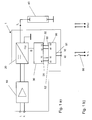
- Fig. 1a shows an inventively designed electronic ballast 1 in a schematic diagram.
- a mains-powered rectifier 10 which the mains voltage in a rectified DC link voltage converts and outputs to an inverter 20.
- the inverter 20 may be formed, for example, as a half-bridge with two switches connected in series between a positive supply voltage and ground, which are controlled via the control device designed as a microcontroller 30 alternately for closing and opening via the control line S.
- the load circuit connected to the inverter 20 has a discharge lamp 40 through which a lamp current i L flows after the ignition process.
- Essential to the present invention is the supply of external brightness control information to the microcontroller 30 via an interface device 50.
- the interface device 50 has an input port 51, which in the described embodiment is designed as a two-wire connection to the connections 51a, 51b. In an embodiment not shown, an input port may be provided with more than two ports.
- the interface device 50 is designed such that brightness control information can be applied to the input port 51 both in the form of control signals which are generated by means of a switch or a pushbutton and in the form of external digital control signals.
- Fig. 1b shows in a schematic diagram symbolizes two examples of the provision of such external control signals that can be applied to the port 51.
- a switch 60 connected to mains voltage N, L, external control signals are generated, i. for the duration of the closing of the switch 60, a sinusoidal mains current is emitted.
- a push-button instead of a switch, a push-button may be used, and the push-button or switch may also switch another voltage such as a constant voltage.
- the external control signal generated in this way is generally used in the electronic ballast according to the invention in those cases in which the electronic ballast is used as an independent light control device.
- the supplied external control signals are interpreted by the microcontroller 30 as brightness control information, for example for switching on or off or for dimming the lamp.
- Fig. 1b Right side, the application of an external digital control signal in the form of a DALI (digitally addressable lighting interface) signal indicated symbolized, via which the microcontroller 30 in such applications receives control information, for example, from a central light control device when the ECG as a single component in a lighting system is integrated.
- DALI signals may include, for example, the information for switching on or dimming the lamp or lamps connected to the ECG.
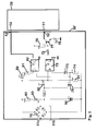
- the interface device 50 of the electronic ballast 10 is embodied such that the control information associated with the external digital control signals is fed to an input port 31 with corresponding input signal terminals 31a, b and the control information associated with the external switching signals is sent to another input port with other input signal terminals 32a, b of the control device 30 be guided.
- the interface device 50 has a first signal path for guiding the control information associated with the external digital control signals from the input port 51 to a first output port 52 having output ports 52a, b and further a second signal path for guiding the control information associated with the external switching signals from the input port 51 to a second output port 53 having output ports 53a, b.
- Each of these output ports 52, 53 is connected to an associated input port or input port 31, 32 of the microcontroller 30. This ensures that at one input port 31, the control information is present for further processing, which corresponds to the external digital control signals and at the other input signal port 32 of the microcontroller 30, the control information is applied, which is associated with the external switching signals, ie corresponding thereto.
- the signal associated with the external DALI signal passes through the phototransistor of the opto-coupler 72 after passing through a signal matching, which by the two resistors 75, 76, the transistor 77 and the diode 78 is realized, on the associated input port 31 of the microcontroller 30.
- the signal waveform described corresponds to the signal path within the interface device 50 on which the control signal is passed, which is the external digital control signal, which is applied to the input port 51 , corresponds.
- the zener diode 80 is designed so that its threshold voltage is greater than the maximum voltage amplitude of the digital signal applied to the input port 51, so that the diode blocks the other signal path for control signals. In the example described, the threshold voltage of the Zener diode is 24V.
- this signal is rectified via the component 70 and can open the second signal path on reaching the threshold voltage at the Zener diode 80, the further via the resistor 81, the photodiode of the optocoupler 82 and the resistor 74 runs.
- the signal associated with the external control signal passes via the phototransistor of the optocoupler 82 to the input port 32 of the microcontroller 30.
- the control information which is assigned to the external control signal and applied to the input port 51 of the interface device 50 is thus fed to the assigned input port 32 of the controller.
- the transistor 79 is turned on, whereby the transistor 71 blocks, so that the first-described signal path is interrupted is. If the external control signal has a sequence of rectangular voltage pulses with an amplitude which is greater than the threshold voltage of the zener diode 80, it is ensured at any time that only one of the two described signal paths to the input port 32 or to the input port 31 is opened.
- Fig. 3 illustrated embodiment of an electronic ballast according to the invention are used, wherein also in FIG. 3 For clarity of illustration only the components microcontroller 30 and the interface device 50 'are shown. Regarding Fig. 2 same components are in Fig. 3 provided with the same reference numerals.
- a normally-off transistor 90 is arranged in the current path which carries the signal associated with the external digital control signal.
- This transistor 90 is switched by a delay element, which is arranged parallel to the input port 51 and the resistor 92, the diode 93 and the integrator capacitor 94 includes, which can transfer the self-locking transistor 90 in the conductive state after a corresponding charge.
- both signal paths of the interface device 50 are initially locked.
- the signal path for the signal which is assigned to a switching signal in turn via the components 70, 80, 81, 82 and 74,79 or from the optocoupler 82 to the associated second Input signal port 32 of the microcontroller 30.
- the latter designates the signal path relevant here to the microcontroller for the brightness control information which is assigned to the external switching signals.
- the input signal received at the port 32 is guided via corresponding components to the reference ground.
- the signal path for the signal passes via the components 70, 90, 72, 73 and 74 or from the phototransistor of the opto-coupler 72 via the level adaptation formed by the components 75-78 to the first input port 31 of FIG Mikrocontrollers 30.
- the latter denotes the signal path relevant here to the microcontroller for the brightness control information, which is assigned to the external digital control signals.
- the signal received at the first input port 31 is internally guided via corresponding components to the reference ground within the controller.
- an external digital control signal for example a DALI signal
- the zener diode 80 blocks the non-normally-off switch 90 because the capacitor C1 initially has no voltage.
- the bridge rectifier 70 outputs an average positive voltage at which the capacitor C1 is charged. After the voltage across the capacitor has been reached in order to drive the transistor 90 for conduction, the signal path for the digital signal is enabled, ie opened, and thus lies against the input port 31 of the microcontroller 30.
- the amount of time necessary to turn on the normally-off transistor 90 depends on the time constant of the RC element and the structure of the digital signal itself. Also at the in Fig. 3 illustrated embodiment is as with reference to Fig. 2 explains, the threshold of the zener diode 80 is set so that it can not be reached when applying an external digital signal at the input port 51, so that the signal path associated with a switching signal is not open.
- the control signals input to the ECG at the input port 51 are switching signals. Will these switching signals as related to Fig. 1b described by switching mains voltage generated, thus is a network pulse train with a frequency of 50 Hz at the input port 51 at.
- This pulse sequence is rectified by means of the bridge 70.
- the capacitor 94 is charged via the resistor 92 and the diode 93.
- the time constant of the delay element is set accordingly.
- the switch 90 It is determined by the resistor 92 and the capacitor 94, and adjusted so that the switch 90 can not go into the conductive state before the threshold voltage of the zener diode 80 is reached and thus the signal path for the external switching signals associated signal is open. Due to the current flow through the resistor 74, the transistor 79 is turned on and thus discharges the capacitor 94, so that the transistor 90 can not go into the conductive state. In the manner described it is ensured that the switch 90 remains locked in any case when the described external switching signal is present at the input port 51. Thus it can be achieved that at no time a signal at the input port 31 of the microcontroller 30 is applied, so that undetermined states can be avoided in the controller.
- an AD converter can also be provided in the signal path which includes the optocoupler 82, so that the input port 32 of the microcontroller 30 in this case is designed to process digital signals.
Abstract
Description
Die Erfindung betrifft ein elektronisches Vorschaltgerät zum Betreiben einer Lampe, mit einer Schnittstellenvorrichtung, welche eingangsseitig eine Anschlusseinrichtung zum Empfang von extern zugeführten Helligkeits-Steuerinformation in Form von externen Steuersignalen aufweist, sowie mit einer Steuereinrichtung, welche mit der Schnittstellenvorrichtung zum Empfang von Helligkeits-Steuerinformation verbunden und zum Ansteuern der Helligkeit der Lampe in Abhängigkeit der empfangenen Helligkeits-Steuerinformation ausgebildet ist, sowie ein Verfahren, für den Betrieb eines solchen Vorschaltgerätes.The invention relates to an electronic ballast for operating a lamp, with an interface device, which has on the input side a connection device for receiving externally supplied brightness control information in the form of external control signals, and with a control device which is connected to the interface device for receiving brightness control information and configured to drive the brightness of the lamp in response to the received brightness control information, and a method of operating such a ballast.
Derartige elektronische Vorschaltgeräte (EVG) sind insbesondere für den Betrieb von Gasentladungslampen, Hochdruckentladungslampen oder Leuchtdioden (LED) geeignet, wobei sie aufgrund des Vorsehens der Schnittstellenvorrichtung flexibel einsetzbar sind. Dadurch, dass sie sowohl zum Empfang von externen Steuersignalen eingerichtet sind, welche durch Schalter bzw. Taster erzeugbar sind, als auch zum Empfang von externen digitalen Steuersignalen, können derartige EVGs sowohl als eigenständiges Lichtsteuergerät als auch als Vorschaltgerät als einzelne Komponente einer lichttechnischen Anlage zum Betrieb einer oder mehrerer Lampen eingesetzt werden. Bei der ersten Anwendung wird in der Regel die Helligkeits-Steuerinformation mittels eines Schalters oder eines Tasters erzeugt und an das EVG übermittelt; bei der zweiten Anwendung kann das EVG beispielsweise von einer zentralen Anlagensteuerung digitale Steuersignale, insbesondere Signale nach dem DALI- (digital addressable lighting interface) -Standard empfangen und in Abhängigkeit dieser Helligkeits-Steuerinformation die Helligkeit der Lampe steuern.Such electronic ballasts (ECG) are particularly suitable for the operation of gas discharge lamps, high-pressure discharge lamps or light-emitting diodes (LED), where they can be used flexibly due to the provision of the interface device. The fact that they are set up both for receiving external control signals which can be generated by switches or buttons, as well as for receiving external digital control signals, such ECGs both as an independent light control device and as a ballast as a single component of a lighting system for operation one or more lamps are used. In the first application, the brightness control information is usually generated by means of a switch or a button and transmitted to the TOE; In the second application, the ECG can, for example, from a central system control digital control signals, in particular Receive signals according to the DALI (digital addressable lighting interface) standard and control the brightness of the lamp in response to this brightness control information.
Ein solches bekanntes EVG ist beispielsweise in der deutschen Patentanmeldung
Der vorliegenden Erfindung liegt die Aufgabe zugrunde, die bestehenden Nachteile herkömmlicher elektronischer Vorschaltgeräte zumindest teilweise zu beheben.The present invention has for its object to at least partially overcome the existing disadvantages of conventional electronic ballasts.
Diese Aufgabe löst die vorliegende Erfindung vorrichtungsseitig schon mit einem elektronischen Vorschaltgerät mit den Merkmalen von Anspruch 1. Das erfindungsgemäße EVG zeichnet sich dadurch aus, dass die Schnittstellenvorrichtung einen ersten Signalpfad aufweist zum Führen von Helligkeits-Steuerinformation, welche externen digitalen Steuersignalen zugeordnet ist, an einen ersten Eingangssignalanschluss der Steuereinrichtung und einen zweiten, vom erster zumindest abschnittsweise unterschiedlichen Signalpfad zum Führen von Helligkeits-Steuerinformation, welche externen, als Schaltsignale ausgebildeten Steuersignalen an einen zweiten, zum ersten unterschiedlichen Eingangssignalanschluss der Steuereinrichtung, und dass die Schnittstellenvorrichtung ein Mittel aufweist zum Erkennen der Steuersignalstruktur des extern zugeführten Steuersignals sowie zum Öffnen des Signalpfades, welcher der erkannten Signalstruktur zugeordnet ist, und/oder zum Blockieren eines Signalpfades, welcher der erkannten Signalstruktur nicht zugeordnet ist.This object is achieved on the device side already with an electronic ballast having the features of claim 1. The ECG according to the invention is characterized in that the interface device has a first signal path for guiding brightness control information, which is assigned to external digital control signals to a first input signal terminal of the control device and a second, from the first at least partially different signal path for guiding brightness control information, which external control signals designed as switching signals to a second, the first different input signal terminal of the control device, and that the interface device comprises means for detecting the control signal structure the externally supplied control signal and to open the signal path, which is associated with the detected signal structure, and / or blocking a signal path which is not associated with the detected signal structure.
Mit der beschriebenen Gestaltung des erfindungsgemäßen EVGs wird erreicht, dass einerseits das empfangene externe Steuersignal, welches einer Helligkeits-Steuerinformation zugeordnet ist, d.h. eine solche darstellt, an einen zugeordneten Eingangsport der Steuereinrichtung angelegt wird und nachfolgend mit Kenntnis auf die Signalstruktur des anliegenden Steuersignals die Verarbeitung der zugeordneten Steuerinformation durchgeführt werden kann. Steuersignale einer bestimmten Signalstruktur werden dadurch dem zugeordneten Eingangsport der Steuereinrichtung zugeführt, sodass diese nicht mehr zur Differenzierung der verschiedenen Steuersignalstrukturen ausgelegt sein muss. Dabei weist die Schnittstellenvorrichtung Mittel zum Erkennen der verschiedenen Steuersignalstrukturen des extern zugeführten Steuersignals auf, weil jeweils eine Signalstruktur einem bestimmten Signalpfad innerhalb der Schnittstellenvorrichtung zugeordnet ist. Nach dem Erkennen der Signalstruktur kann das jeweilige Steuersignal gezielt auf dem zugeordneten und vorbestimmten Signalpfad geführt und damit dem zugeordneten und vorbestimmten Eingangssignalanschluss der Steuereinrichtung zugeführt werden kann.With the described design of the electronic ballast according to the invention it is achieved that, on the one hand, the received external control signal, which is assigned to a brightness control information, i. represents such, is applied to an associated input port of the control device and subsequently with knowledge of the signal structure of the applied control signal, the processing of the associated control information can be performed. Control signals of a specific signal structure are thereby supplied to the associated input port of the control device, so that it no longer has to be designed to differentiate the various control signal structures. In this case, the interface device has means for detecting the different control signal structures of the externally supplied control signal, because in each case a signal structure is assigned to a specific signal path within the interface device. After the signal structure has been detected, the respective control signal can be guided in a targeted manner on the assigned and predetermined signal path and thus supplied to the assigned and predetermined input signal connection of the control device.
Es sei darauf hingewiesen, dass die Schnittstellenvorrichtung des erfindungsgemäßen EVGs nicht auf zwei Signalpfade für externe Steuersignale beschränkt ist, die jeweils einer Signalstruktur zugeordnet sind. Es können auch weitere derartige Signalpfade zur Differenzierung unterschiedlicher Strukturen von externen Steuersignalen umfasst sein, wobei die Steuereinrichtung dann eine an die Zahl der Signalpfade angepasste Anzahl von Steuereingängen aufweisen kann.It should be noted that the interface device of the electronic ballast according to the invention is not limited to two signal paths for external control signals, which are each assigned to a signal structure. It is also possible to include further such signal paths for differentiating different structures from external control signals, wherein the control device can then have a number of control inputs adapted to the number of signal paths.
Die Zuordnung einer Helligkeits-Steuerinformation zu den jeweiligen externen Steuersignalen kann beispielsweise dadurch realisiert sein, dass diese Steuerinformation in einer vorgegebenen Weise im zugehörigen externen Steuersignal kodiert ist. Dementsprechend ist aus einem solchen Steuersignal die zugeordnete Helligkeits-Steuerinformation decodierbar bzw. die Steuerinformation lässt sich aus dem Steuersignal herleiten. Vorzugsweise bleibt der Helligkeits-Steuerinformationsgehalt des Signals vollständig erhalten, wenn es auf dem zugeordneten, d.h. zugehörigen Signalpfad innerhalb der Schnittstellenvorrichtung geführt wird, wobei auf diesem Signalpfad z.B. auch eine Umwandlung oder Umsetzung des Signals erfolgen kann.The assignment of brightness control information to the respective external control signals can be achieved, for example be realized that this control information is encoded in a predetermined manner in the associated external control signal. Accordingly, the associated brightness control information can be decoded from such a control signal or the control information can be derived from the control signal. Preferably, the brightness control information content of the signal is completely retained when it is carried on the associated, ie associated signal path within the interface device, wherein on this signal path, for example, a conversion or conversion of the signal can take place.
Besonders zweckmäßig ist es, wenn die eingangsseitige Anschlusseinrichtung der Schnittstelleneinrichtung zum Empfang von extern zugeführten Helligkeits-Steuerinformation, d.h. zum Empfang der extern zugeführten Steuersignale als Zweidraht-Anschluss ausgebildet ist, was den Anschluss an die externe Steuersignalbereitstellung vereinfacht. Besonders zweckmäßig ist es dabei, wenn sowohl die durch einen Schalter oder einen Taster erzeugten Steuersignale als auch die digitalen Steuersignale über die gleichen Eingangsanschlüsse der Anschlusseinrichtung, insbesondere über den besagten Zweidraht-Anschluss an das EVG anlegbar sind. In der Regel werden dabei entweder die durch einen Schalter oder einen Taster erzeugten und damit als Schaltsignale ausgebildeten Steuersignale oder die digitalen Steuersignale an den Zweidraht-Anschluss angelegt, je nachdem, ob das erfindungsgemäße EVG beispielsweise als eigenständiges Lichtsteuergerät oder als Komponente in einer lichttechnischen Anlage eingesetzt ist.It is particularly expedient if the input-side connection device of the interface device for receiving externally supplied brightness control information, i. for receiving the externally supplied control signals is designed as a two-wire connection, which simplifies the connection to the external control signal provision. It is particularly expedient if both the control signals generated by a switch or a button and the digital control signals via the same input terminals of the terminal device, in particular via said two-wire connection to the ECG can be applied. As a rule, either the control signals generated by a switch or a push button and thus designed as switching signals or the digital control signals are applied to the two-wire connection, depending on whether the inventive ballast used, for example, as an independent light control device or as a component in a lighting system is.
Das von der Schnittstellenvorrichtung empfangene Steuersignal wird innerhalb der Vorrichtung in Bezug auf seine Struktur untersucht und einer der möglichen Strukturen zugeordnet. Hierzu weist die Schnittstellenvorrichtung das besagte Mittel zum Erkennen der Steuersignalstruktur des extern zugeführten Steuersignals auf. Dieses Mittel ist geeignet, einen prinzipiell beliebigen Parameter des Signals zu erfassen und zu differenzieren, beispielsweise das Frequenzverhalten und/oder die Amplitude des Signals. Insofern kann es zweckmäßig sein, wenn das Mittel zum Erkennen der Steuersignalstruktur des extern zugeführten Steuersignals sowie zum Öffnen des Signalpfades, welcher der erkannten Signalstruktur zugeordnet ist, eine Einrichtung zur Schwellwerterkennung mit zugeordnetem Schalter, eine Mikrocontrollereinrichtung zur Signalauswertung mit zugeordneter und von dieser gesteuerter Schaltereinrichtung und/oder eine Frequenzweiche aufweist, wodurch das Steuersignal über den zugeordneten Signalpfad an den entsprechenden Eingangssignalanschluss der Steuereinrichtung geleitet werden kann.The control signal received by the interface device is examined within the device with respect to its structure and assigned to one of the possible structures. For this purpose, the interface device on the said means for detecting the control signal structure of the externally supplied control signal. This agent is suitable to detect and differentiate in principle any parameter of the signal, for example the frequency response and / or the amplitude of the signal. In this respect, it may be expedient if the means for detecting the control signal structure of the externally supplied control signal and for opening the signal path, which is associated with the detected signal structure, a device for threshold detection with associated switch, a microcontroller device for signal evaluation with associated and controlled by this switch device and / or a crossover, whereby the control signal can be passed via the associated signal path to the corresponding input signal terminal of the control device.
In einer besonders kostengünstige Ausführungsform kann das Mittel zum Erkennen der Steuersignalstruktur des extern zugeführten Steuersignals sowie zum Öffnen des dem Steuersignal zugeordneten Signalpfades eine Zenerdiode umfassen, welche beim Vorliegen einer vorgegebenen Schwellspannung in den leitenden Zustand übergeht. Eine solche Ausführungsform ist besonders dann zweckmäßig, wenn sich die zu differenzierenden Steuersignalstrukturen insbesondere in der Spannungsamplitude unterscheiden, sodass mit dem Vorsehen einer Zenerdiode festgelegt werden kann, dass erst beim Vorliegen einer Spannung die größer als die Schwellspannung der Zenerdiode ist, der entsprechende Signalpfad geöffnet wird. Einer Steuersignalstruktur, welche eine niedrigere Spannungsamplitude besitzt, bzw. einem Steuersignal mit einer solchen Signalstruktur, bleibt ein solcher, eine Zenerdiode aufweisender Signalpfad versperrt.In a particularly cost-effective embodiment, the means for detecting the control signal structure of the externally supplied control signal and for opening the signal path associated with the control signal may comprise a zener diode which changes to the conducting state when a predetermined threshold voltage is present. Such an embodiment is particularly expedient if the control signal structures to be differentiated differ in particular in the voltage amplitude, so that it can be determined by providing a zener diode that the corresponding signal path is opened only when a voltage greater than the threshold voltage of the zener diode is present , A control signal structure which has a lower voltage amplitude, or a control signal with such a signal structure, remains blocked by such a signal path having a Zener diode.
Zum Öffnen des jeweiligen, der erkannten Signalstruktur zugeordneten Signalpfades kann die Schnittstelleneinrichtung zumindest einen Schalter aufweisen, welcher den jeweiligen Signalpfad an den zugehörigen Eingangsport der Steuereinrichtung schaltet. Ein solcher Schalter kann, wie beim beschriebenen Beispiel der Zenerdiode selbstgesteuert sein. Es ist jedoch auch möglich, einen Schalter mit einem Steuereingang zu verwenden, wobei dieser insbesondere über das externe Steuereingangssignal der Schnittstellenvorrichtung oder über ein davon abgeleitetes Signal gesteuert sein kann.To open the respective signal path assigned to the recognized signal structure, the interface device can have at least one switch which switches the respective signal path to the associated input port of the control device. Such a switch can be self-controlled, as in the described example of the zener diode. It However, it is also possible to use a switch with a control input, which can be controlled in particular via the external control input signal of the interface device or via a signal derived therefrom.
Besonders zweckmäßig ist es, wenn sowohl für den ersten als auch für den zweiten Signalpfad jeweils zumindest ein Schalter umfasst ist, wobei sich beide Schalter im Ruhezustand, insbesondere nach einer Betriebsinitialisierung des Vorschaltgerätes, in einem nicht leitenden Zustand befinden. Damit ist sichergestellt, dass vor dem Erkennen der Signalstruktur des externen Steuersignals kein Signalpfad geöffnet ist, wodurch wiederum sichergestellt werden kann, dass nicht zufällig ein externes Steuersignal am falschen Steuersignaleingang der Steuereinrichtung zur Anlage kommt.It is particularly expedient if in each case at least one switch is included for both the first and the second signal path, wherein both switches are in a non-conducting state in the idle state, in particular after an operational initialization of the ballast. This ensures that no signal path is opened before the detection of the signal structure of the external control signal, which in turn can ensure that not accidentally an external control signal at the wrong control signal input of the control device comes to rest.
Um eine solche Fehlleitung des externen Steuersignals über einen diesem Signal, bzw. seiner Signalstruktur nicht zugeordneten Signalpfad und damit an einen nicht zugeordneten Steuersignaleingang der Steuereinrichtung zu vermeiden, kann es ferner, insbesondere beim Vorliegen von zeitlich veränderlichen Steuersignalen, wie einem Tastersignal mit einer Modulation von beispielsweise 50 Hz, 60 Hz oder 100 Hz vorteilhaft sein, wenn ein Schalter eines Signalpfades über ein Verzögerungsglied ansteuerbar ist, wobei zweckmäßigerweise am Verzögerungsglied das externe Steuersignal oder ein davon abgeleitetes Signal anliegt. Hierdurch können auch ansonsten kurzzeitig auftretende Fehlführungen des externen Steuersignals bzw. der diesem Signal zugeordnete Steuerinformation vermieden werden, was Fehlinterpretationen in der Steuereinrichtung verhindert. Bei einer solchen Ausführungsform kann das Verzögerungsglied beispielsweise als RC-Glied ausgebildet sein, wobei der Kondensator durch das anliegende externe Steuersignal oder ein daraus abgeleitetes Signal geladen wird und die Spannung am Kondensator als Schaltspannung zum Öffnen eines Signalpfades eingesetzt ist.In order to avoid such a misdirection of the external control signal via a signal path not assigned to this signal or its signal structure and thus to an unassigned control signal input of the control device, it can also, in particular in the presence of time-varying control signals, such as a push-button signal with a modulation of For example, 50 Hz, 60 Hz or 100 Hz be advantageous if a switch of a signal path can be controlled via a delay element, wherein expediently applied to the delay element, the external control signal or a signal derived therefrom. As a result, otherwise erroneous guides of the external control signal or the control information associated with this signal can be avoided, which prevents misinterpretations in the control device. In such an embodiment, the delay element may be formed, for example, as an RC element, wherein the capacitor is charged by the applied external control signal or a signal derived therefrom and the voltage on the capacitor is used as a switching voltage for opening a signal path.
Zur Vermeidung eines unerwünschten Zustandes an einem Eingangssignalanschluss der Steuereinrichtung kann es ferner zweckmäßig sein, wenn das erfindungsgemäße Vorschaltgerät so ausgebildet ist, dass nach dem Öffnen eines der beiden Signalpfade der andere Signalpfad automatisch blockiert wird.To avoid an undesirable state at an input signal terminal of the control device, it may also be useful if the ballast according to the invention is designed so that after opening one of the two signal paths of the other signal path is automatically blocked.
Vorteilhaft kann vorgesehen sein, dass zumindest einer der Signalpfade in der Schnittstellenvorrichtung elektronische Bauteile zur Umformung des auf diesem Signalpfad geführten Steuersignals ausgebildet ist. Beispielsweise kann vorgesehen sein, zur galvanischen Entkopplung einen Optokoppler oder einen DC/DC-Wandler vorzusehen. Darüber hinaus ist es jedoch auch möglich, in einem Signalpfad Signal-Umformbauteile zu verwenden, wie einen A/D-Wandler oder einen U/f-Wandler mit nachfolgender Digitalisierung, sodass beispielsweise ein analoges Tastersignal, das von der Schnittstellenvorrichtung empfangen wird und welches aufgrund seiner Signalstruktur einem der beiden Signalpfade in der Schnittstellenvorrichtung, damit einem bestimmten Eingangssignalanschluss der Schnittstellenvorrichtung zugeordnet ist und diesem zugeführt wird, im Laufe seiner Signaltransmission durch die Schnittstellenvorrichtung in ein digitales Signal umgewandelt wird, das jedoch bezüglich seiner Steuerinformation weiterhin dem Tastersignal des Schalters entspricht. Auf diese Weise ist es beispielsweise möglich, dass beide Eingangssignalanschlüsse an der Steuereinrichtung zum Aufnehmen von digitalen Steuersignalen eingerichtet sind, wobei über den zweiten Signalpfad das digitalisierte Steuersignal an den zweiten Eingangssignalanschluss der Steuereinrichtung angelegt ist. Durch eine derartige Umformung können die externen Steuersignale an die jeweilige Steuereinrichtung angepasst werden.Advantageously, it can be provided that at least one of the signal paths in the interface device has electronic components for transforming the control signal carried on this signal path. For example, it may be provided to provide an optocoupler or a DC / DC converter for galvanic decoupling. In addition, however, it is also possible to use in a signal path signal shaping components, such as an A / D converter or a V / f converter with subsequent digitization, so that, for example, an analogue probe signal, which is received by the interface device and which due Its signal structure one of the two signal paths in the interface device, so that a particular input signal terminal of the interface device is assigned and this is supplied, is converted in the course of its signal transmission by the interface device into a digital signal, which, however, with respect to its control information corresponds to the button signal of the switch. In this way it is possible, for example, for both input signal connections to be set up on the control device for receiving digital control signals, wherein the digitized control signal is applied to the second input signal connection of the control device via the second signal path. By such a transformation, the external control signals can be adapted to the respective control device.
Vorzugsweise können die im Rahmen der Erfindung verwendeten Schalter als Halbleiterschalter wie Transistoren ausgebildet sein.Preferably, the switches used in the invention may be formed as semiconductor switches such as transistors.
Verfahrensseitig löst die Erfindung die obige Aufgabe mit einem Verfahren zum Betrieb eines elektronischen Vorschaltgerätes zum Treiben einer Lampe, mit einer Schnittstellenvorrichtung, die eingangsseitig extern zugeführte Helligkeits-Steuerinformation in Form von Steuersignalen empfängt, sowie mit einer Steuereinrichtung, zu welcher Helligkeits-Steuerinformation weitergeleitet wird und welche die Helligkeit der Lampe in Abhängigkeit der empfangenen Steuerinformation steuert. Das erfindungsgemäße Verfahren zeichnet sich dadurch aus, dass die Steuereinrichtung an einem ersten Eingangssignalanschluss Helligkeits-Steuerinformation, welche externen digitalen Steuersignale zugeordnet ist, über einen ersten Signalpfad der Schnittstellenvorrichtung zur Verarbeitung empfängt und ferner an einem zweiten Eingangssignalanschluss über einen zweiten Signalpfad der Schnittstellenvorrichtung Helligkeits-Steuerinformation, welche als externe Schaltsignale ausgebildeten Steuersignalen zugeordnet ist, zur Verarbeitung empfängt, wobei in der Schnittstellenvorrichtung die Signalstruktur eines externen Steuersignals erkannt und in Abhängigkeit der erkannten Signalstruktur der dieser Signalstruktur zugeordnete Signalpfad geöffnet wird und/oder ein Signalpfad blockiert wird, welcher der erkannten Signalstruktur nicht zugeordnet ist.In terms of the method, the invention solves the above object with a method for operating an electronic ballast for driving a lamp, with an interface device receiving externally supplied brightness control information on the input side in the form of control signals, and with a control device to which brightness control information is forwarded and which controls the brightness of the lamp in response to the received control information. The inventive method is characterized in that the control device at a first input signal terminal brightness control information, which external digital control signals is assigned via a first signal path of the interface device for processing and further at a second input signal terminal via a second signal path of the interface device brightness control information , which is associated with control signals designed as external switching signals, the signal structure of an external control signal being detected in the interface device and opened depending on the detected signal structure of the signal path associated with this signal structure and / or blocking a signal path which does not block the detected signal structure assigned.
Soweit in der vorliegenden Anmeldung der Ausdruck "Steuersignal über einen ersten Signalpfad" verwendet wird, meint dieser nicht nur das ursprüngliche, von der Schnittstellenvorrichtung empfangene externe digitale Steuersignal, sondern auch ein eventuell aus diesem externen digitalen Steuersignal hergeleitetes, abgeleitetes oder umgewandeltes Signal. Eine solche Umwandlung kann beispielsweise über einen A/D-Wandler, einen D/A-Wandler, einen DC/DC-Wandler und/oder über einen Optokoppler durchgeführt werden. In gleicher Weise beschreibt die Bezeichnung "Steuersignal über einen zweiten Signalpfad" nicht nur das an der Schnittstellenvorrichtung eingangsseitig empfangene, als Schaltsignal ausgebildete Steuersignal, sondern auch das im Verlauf der Führung über den zweiten Signalpfad eventuell daraus abgeleitete Steuersignal, welches über dem zweiten Signalpfad zum zugeordneten zweiten Eingangssignalanschluss der Steuereinrichtung geführt ist. Darüber hinaus sei bemerkt, dass die in diesem Zusammenhang verwendeten Begriffe wie "erster" bzw. "zweiter" allein der Differenzierung dienen, jedoch keine Beschränkung in Bezug auf eine Reihenfolge oder dergleichen angeben.As used in this application, the term "control signal over a first signal path" means not only the original external digital control signal received from the interface device but also any derived, derived or converted signal from that external digital control signal. Such a conversion can be carried out, for example, via an A / D converter, a D / A converter, a DC / DC converter and / or via an optocoupler. In the same way, the term "control signal via a second signal path" not only describes that at the interface device On the input side received, designed as a switching signal control signal, but also in the course of leadership on the second signal path, possibly derived therefrom control signal, which is guided over the second signal path to the associated second input signal terminal of the control device. In addition, it should be noted that the terms used in this context, such as "first" and "second", respectively, are for the purpose of differentiation only, but are not intended to limit the order or the like.
Die Erfindung wird im Folgenden durch das Beschreiben mehrerer Ausführungsformen und weiterer erfindungswesentlicher Merkmale unter Bezugnahme auf die beiliegenden Zeichnungen erläutert, wobei
- Fig. 1a
- in einer Prinzipskizze ein erfindungsgemäß ausgebildetes elektronische Vorschaltgerät,
- Fig. 1b
- in einer Prinzipdarstellung zwei unterschiedliche externe Steuersignale symbolisiert,
- Fig. 2
- in einer Detailansicht eine Schnittstellenvorrichtung sowie den daran angeschlossenen Mikrocontroller einer Ausführungsform eines erfindungsgemäßen elektronischen Vorschaltgerätes und
- Fig. 3
- in einer Detailansicht eine Schnittstellenvorrichtung sowie den daran angeschlossenen Mikrocontroller einer weiteren Ausführungsform eines erfindungsgemäßes elektronischen Vorschaltgerätes,
- Fig. 1a
- in a schematic diagram of an inventively designed electronic ballast,
- Fig. 1b
- symbolizes two different external control signals in a schematic representation,
- Fig. 2
- in a detailed view of an interface device and the connected microcontroller of an embodiment of an electronic ballast according to the invention and
- Fig. 3
- in a detailed view of an interface device and the microcontroller connected thereto of a further embodiment of an inventive electronic ballast,
Für die vorliegende Erfindung wesentlich ist die Zuführung von externer Helligkeits-Steuerinformation an den Mikrocontroller 30 über eine Schnittstellenvorrichtung 50. Hierzu weist die Schnittstellenvorrichtung 50 einen Eingangsport 51 auf, der in der beschriebenen Ausführungsform als Zweidraht-Anschluss mit den Anschlüssen 51a, 51b ausgebildet ist. In einer nicht gezeigten Ausführungsform kann ein Eingangsport mit mehr als zwei Anschlüssen vorgesehen sein. Die Schnittstellenvorrichtung 50 ist erfindungsgemäß so ausgebildet, dass an den Eingangsport 51 Helligkeits-Steuerinformation sowohl in Form von Steuersignalen, welche mittels eines Schalters oder eines Tasters erzeugt werden, als auch in Form von externen, digitalen Steuersignale anlegbar sind.Essential to the present invention is the supply of external brightness control information to the
Beim linken Beispiel wird mittels eines Schalters 60, welcher an Netzspannung N,L angeschlossen ist, externe Steuersignale erzeugt, d.h. für die Dauer des Schließens des Schalters 60 wird ein sinusförmiger Netzstrom abgegeben. In einer anderen Ausführungsform kann statt eines Schalters ein Taster verwendet werden, ferner kann der Taster oder der Schalter auch eine andere Spannung wie beispielsweise eine konstante Spannung schalten. Das so erzeugte externe Steuersignal wird in der Regel bei dem erfindungsgemäßen EVG in solchen Fällen verwendet, bei welchen das EVG als selbstständiges Lichtsteuergerät Verwendung findet. Die zugeführten externen Steuersignale werden von dem Mikrocontroller 30 als Helligkeits-Steuerinformation interpretiert, beispielsweise zum Ein- bzw. Ausschalten oder auch zum Dimmen der Lampe.In the left example, by means of a
In
Die Schnittstellenvorrichtung 50 des erfindungsgemäßen EVGs 10 ist so ausgebildet, dass die den externen digitalen Steuersignalen zugeordnete Steuerinformation an einen Eingangsport 31 mit entsprechenden Eingangssignalanschlüssen 31a, b geführt und die den externen Schaltsignalen zugeordnet Steuerinformation an einen anderen Eingangsport mit anderen Eingangssignalanschlüssen 32a,b der Steuereinrichtung 30 geführt werden. Hierzu weist die Schnittstellenvorrichtung 50 einen ersten Signalpfad auf zum Führen der den externen digitalen Steuersignalen zugeordneten Steuerinformation vom Eingangsport 51 an einen ersten Ausgangsport 52 mit Ausgangsanschlüssen 52a, b und ferner einen zweiten Signalpfad zum Führen der den externen Schaltsignalen zugeordneten Steuerinformation vom Eingangsport 51 an einen zweiten Ausgangsport 53 mit Ausgangsanschlüssen 53a, b. Jeder dieser Ausgangsports 52, 53 ist mit einem zugeordneten Eingangsport oder Eingangsanschluss 31, 32 des Mikrocontrollers 30 verbunden. Damit ist sichergestellt, dass an dem einen Eingangsport 31 die Steuerinformation zur Weiterverarbeitung anliegt, welche den externen digitalen Steuersignalen entspricht und an dem anderen Eingangssignalport 32 des Mikrocontrollers 30 die Steuerinformation anliegt, welche den externen Schaltsignalen zugeordnet ist, d.h. diesen entspricht.The
Um eine Trennung der unterschiedlichen Steuersignale innerhalb der Schnittstellenvorrichtung 50 bereitzustellen, weist diese in der dargestellten Ausführungsform ein Mittel zum Erkennen der Steuersignalstruktur des extern zugeführten Steuersignals sowie zum Öffnen eines der beiden Signalpfade auf, welcher der erkannten Steuersignalstruktur zugeordnet ist. Ausführungsbeispiele hierzu werden nun mit Bezug auf die
Dabei wird davon ausgegangen, dass an dem Eingangsport 51 der Schnittstellenvorrichtung 50 die mit Bezug auf
Liegt jedoch am Eingangsport 51 das obenstehend mit Bezug auf
Um zu vermeiden, dass das anliegende externe Schaltsignal zu einem Signal am Eingangsport 31 des Mikrocontrollers 30 führt, wird mit dem Öffnen des zweiten Signalpfades der Transistor 79 leitend geschaltet, wodurch der Transistor 71 sperrt, sodass der erstbeschriebene Signalpfad unterbrochen ist. Wenn das externe Steuersignal eine Abfolge von rechteckförmigen Spannungspulsen aufweist mit einer Amplitude, die größer als die Schwellspannung der Zenerdiode 80 ist, ist zu jedem Zeitpunkt sichergestellt, dass jeweils nur einer der beiden beschriebenen Signalpfade zum Eingangsport 32 bzw. zum Eingangsport 31 geöffnet ist.In order to avoid that the applied external switching signal leads to a signal at the
Um ein gleichzeitiges Öffnen beider Signalpfade auch in solchen Fällen sicherzustellen, bei welchen das externe Steuersignal als Schaltsignal mit einer Abfolge von insbesondere sinusförmigen Spannungspulsen gebildet ist, kann die in
Der wesentliche Unterschied zwischen den Schnittstellenvorrichtungen 50 gemäß
Wird nun ein externes digitales Steuersignal, beispielsweise ein DALI-Signal an den Eingangsport 51 der Schnittstellenvorrichtung 50' angelegt, sind mit den obigen Erläuterungen zu den beiden Signalpfaden zunächst beide gesperrt. Die Zenerdiode 80 sperrt, da die Eingangsspannung geringer als die Schwellspannung ist, der nicht selbstleitende Schalter 90 gesperrt, da der Kondensator C1 zunächst keine Spannung aufweist. Unabhängig davon, ob das anliegende externe digitale Steuersignal monopolar oder bipolar aufgebaut ist, gibt der Brückengleichrichter 70 eine mittlere positive Spannung ab, mit welcher der Kondensator C1 geladen wird. Nachdem die Spannung am Kondensator erreicht ist, um den Transistor 90 zur Leitung anzusteuern, ist der Signalpfad für das digitale Signal freigeschaltet, d.h. geöffnet und liegt damit am Eingangsport 31 des Mikrocontrollers 30 an. Die Zeitdauer, welche notwendig ist, um den selbstsperrender Transistor 90 durchzuschalten, hängt von der Zeitkonstante des RC-Gliedes sowie dem Aufbau des digitalen Signals selbst ab. Auch bei der in
Wird dagegen das EVG eigenständig benutzt, sind die an das EVG am Eingangsport 51 eingegebenen Steuersignale Schaltsignale. Werden diese Schaltsignale wie mit Bezug auf
31 des Mikrocontrollers 30 anliegt, sodass unbestimmte Zustände im Controller vermieden werden können.If, however, the ECG is used independently, the control signals input to the ECG at the
31 of the
In nicht angegebenen Ausführungsformen können in den beiden Signalpfaden auch andere Signalumformungen vorgesehen werden. Beispielsweise kann in dem Signalpfad, welcher den Optokoppler 82 umfasst, auch ein AD-Wandler vorgesehen sein, sodass der Eingangsport 32 des Mikrocontrollers 30 in diesem Fall zum Verarbeiten von digitalen Signalen ausgebildet ist.In non-specified embodiments, other signal transformations can be provided in the two signal paths. By way of example, an AD converter can also be provided in the signal path which includes the
- 11
- elektronisches Vorschaltgerät EVGelectronic ballast electronic ballast
- 1010
- Gleichrichterrectifier
- 2020
- Wechselrichterinverter
- 3030
- Mikrocontrollermicrocontroller
- 3131
- erster Eingangsport des Mikrocontrollers / Eingangsanschlussfirst input port of the microcontroller / input port
- 31a,31b31a, 31b
- Eingangssignalanschlüsse des ersten EingangsportsInput signal terminals of the first input port
- 3232
- zweiter Eingangsport des Mikrocontrollers / Eingangsanschlusssecond input port of the microcontroller / input port
- 32a,32b32a, 32b
- Eingangsanschluss / Eingangssignalanschluss des zweiten EingangsportsInput port / input signal port of the second input port
- 4040
- Entladungslampe / LampeDischarge lamp / lamp
- 5050
- SchnittstellenvorrichtungInterface device
- 50'50 '
- SchnittstellenvorrichtungInterface device
- 5151
- Eingangsport der SchnittstellenvorrichtungInput port of the interface device
- 51a,51b51a, 51b
- Eingangssignalanschlüsse der SchnittstellenvorrichtungInput signal terminals of the interface device
- 5252
- erster Ausgangsportfirst exit port
- 52a52a
- Ausgangsanschlussoutput port
- 52b52b
- Ausgangsanschlussoutput port
- 5353
- zweiter Ausgangsportsecond output port
- 53a53a
- Ausgangsanschlussoutput port
- 53b53b
- Ausgangsanschlussoutput port
- 6060
- Schalterswitch
- 7070
- BrückengleichrichterBridge rectifier
- 7171
- selbstleitender Transistorself-conducting transistor
- 7272
- Optokoppleroptocoupler
- 7373
- ZenerdiodeZener diode
- 7474
- Widerstandresistance
- 7575
- Widerstandresistance
- 7676
- Widerstandresistance
- 7777
- Transistortransistor
- 7878
- ZenerdiodeZener diode
- 7979
- Transistortransistor
- 8080
- ZenerdiodeZener diode
- 8181
- Widerstandresistance
- 8282
- Optokoppleroptocoupler
- 9090
- selbstsperrender Transistorself-locking transistor
- 9191
- Widerstandresistance
- 9292
- Widerstandresistance
- 9393
- Diodediode
- 9494
- Kondensatorcapacitor
- iL i L
- Lampenstromlamp current
- (N,L)(N, L)
- Netzspannungmains voltage
- SS
- Steuerleitungcontrol line
Claims (16)
Applications Claiming Priority (1)
| Application Number | Priority Date | Filing Date | Title |
|---|---|---|---|
| DE102010014442A DE102010014442A1 (en) | 2010-04-09 | 2010-04-09 | Electronic ballast with interface device |
Publications (3)
| Publication Number | Publication Date |
|---|---|
| EP2375868A2 true EP2375868A2 (en) | 2011-10-12 |
| EP2375868A3 EP2375868A3 (en) | 2014-12-10 |
| EP2375868B1 EP2375868B1 (en) | 2016-06-15 |
Family
ID=44343757
Family Applications (1)
| Application Number | Title | Priority Date | Filing Date |
|---|---|---|---|
| EP11159492.5A Active EP2375868B1 (en) | 2010-04-09 | 2011-03-24 | Electronic pre-switching device with interface device |
Country Status (4)
| Country | Link |
|---|---|
| EP (1) | EP2375868B1 (en) |
| AU (1) | AU2011201614B2 (en) |
| BR (1) | BRPI1101876A2 (en) |
| DE (1) | DE102010014442A1 (en) |
Cited By (2)
| Publication number | Priority date | Publication date | Assignee | Title |
|---|---|---|---|---|
| CN109462395A (en) * | 2018-12-28 | 2019-03-12 | 常州朗奇威电器有限公司 | Interface multiplexes conversion circuit and multiplexing conversion method |
| EP3764746A1 (en) * | 2019-07-12 | 2021-01-13 | ERCO GmbH | Operating device |
Families Citing this family (1)
| Publication number | Priority date | Publication date | Assignee | Title |
|---|---|---|---|---|
| DE102019125445A1 (en) * | 2019-07-12 | 2021-01-14 | Erco Gmbh | Control gear |
Citations (1)
| Publication number | Priority date | Publication date | Assignee | Title |
|---|---|---|---|---|
| DE19757295A1 (en) | 1997-03-04 | 1998-09-10 | Tridonic Bauelemente | Electronic ballast |
Family Cites Families (5)
| Publication number | Priority date | Publication date | Assignee | Title |
|---|---|---|---|---|
| US5225765A (en) * | 1984-08-15 | 1993-07-06 | Michael Callahan | Inductorless controlled transition and other light dimmers |
| FI95985C (en) * | 1994-11-24 | 1996-04-10 | Helvar Oy | Method and circuit system for controlling an electronics lighting device |
| US5751118A (en) * | 1995-07-07 | 1998-05-12 | Magnetek | Universal input dimmer interface |
| WO2001052607A1 (en) * | 2000-01-14 | 2001-07-19 | Patent-Treuhand-Gesellschaft Für Elektrische Glüh Lampen Mbh | Device for controlling operating means for at least one electric illuminating means and a method for controlling operating means for at least one electric illuminating means |
| DE10319514A1 (en) * | 2003-04-30 | 2004-11-18 | Tridonicatco Gmbh & Co. Kg | Interface for digital and mains voltage signals |
-
2010
- 2010-04-09 DE DE102010014442A patent/DE102010014442A1/en not_active Ceased
-
2011
- 2011-03-24 EP EP11159492.5A patent/EP2375868B1/en active Active
- 2011-04-08 AU AU2011201614A patent/AU2011201614B2/en active Active
- 2011-04-08 BR BRPI1101876-3A patent/BRPI1101876A2/en not_active IP Right Cessation
Patent Citations (1)
| Publication number | Priority date | Publication date | Assignee | Title |
|---|---|---|---|---|
| DE19757295A1 (en) | 1997-03-04 | 1998-09-10 | Tridonic Bauelemente | Electronic ballast |
Cited By (3)
| Publication number | Priority date | Publication date | Assignee | Title |
|---|---|---|---|---|
| CN109462395A (en) * | 2018-12-28 | 2019-03-12 | 常州朗奇威电器有限公司 | Interface multiplexes conversion circuit and multiplexing conversion method |
| CN109462395B (en) * | 2018-12-28 | 2023-08-15 | 常州朗奇威电器有限公司 | Interface multiplexing conversion circuit and multiplexing conversion method |
| EP3764746A1 (en) * | 2019-07-12 | 2021-01-13 | ERCO GmbH | Operating device |
Also Published As
| Publication number | Publication date |
|---|---|
| DE102010014442A1 (en) | 2011-10-13 |
| EP2375868B1 (en) | 2016-06-15 |
| BRPI1101876A2 (en) | 2012-10-02 |
| EP2375868A3 (en) | 2014-12-10 |
| AU2011201614A1 (en) | 2011-10-27 |
| AU2011201614B2 (en) | 2013-08-29 |
Similar Documents
| Publication | Publication Date | Title |
|---|---|---|
| EP2154935B1 (en) | Interface circuit for transmitting digital data in a lighting device | |
| EP2554021A1 (en) | System-voltage transmission branch of an interface of an operating device for light-emitting means | |
| EP2375868B1 (en) | Electronic pre-switching device with interface device | |
| EP3183584A1 (en) | Supply voltage detection device and a method for detecting a supply voltage | |
| DE102013219153A1 (en) | Driver module with secondary-side detection of a primary-side electrical supply | |
| DE3428444C2 (en) | ||
| EP2638783B1 (en) | Interference-free light-emitting means control | |
| EP1954104B1 (en) | Interface for switch signals and digital signals with protective circuit | |
| DE10319514A1 (en) | Interface for digital and mains voltage signals | |
| DE10312704A1 (en) | Method for controlling and monitoring the function of a power semiconductor switch and device for carrying out the method | |
| EP1494507B1 (en) | Digital interface with a potentiometer | |
| WO2011107280A2 (en) | Controllable operational device for light-emitting diodes | |
| EP3603345B1 (en) | Circuit arrangement and method for operating lamps | |
| AT408392B (en) | Control device for an electronic service device | |
| EP2702838B1 (en) | Electronic ballast for an illumination device | |
| DE102007009520B4 (en) | Interface for digital signals and mains voltage signals, with switchable constant current source | |
| WO2015144351A1 (en) | Voltage supply circuit for operating leds | |
| AT508809A1 (en) | INTERFACE FOR A BULB OPERATING DEVICE | |
| DE102015118725B3 (en) | Circuit operating apparatus and method for controlling such a group circuit | |
| EP3895642B1 (en) | Device for coagulation and/or dissection of biological tissue and a method of operating a device. | |
| DE202012008421U1 (en) | Controllable operating device | |
| DE102019127697B4 (en) | Control module for a lamp operating device with a flexible control connection | |
| EP0855035B1 (en) | Operating process for an input circuit and corresponding input circuit | |
| EP2156455A1 (en) | Device and method for identifying the type of control for a voltage- or current-release switchgear | |
| DE19821539C1 (en) | Switching arrangement, and method for recognition and control, of attached electrical load |
Legal Events
| Date | Code | Title | Description |
|---|---|---|---|
| PUAI | Public reference made under article 153(3) epc to a published international application that has entered the european phase |
Free format text: ORIGINAL CODE: 0009012 |
|
| AK | Designated contracting states |
Kind code of ref document: A2 Designated state(s): AL AT BE BG CH CY CZ DE DK EE ES FI FR GB GR HR HU IE IS IT LI LT LU LV MC MK MT NL NO PL PT RO RS SE SI SK SM TR |
|
| AX | Request for extension of the european patent |
Extension state: BA ME |
|
| PUAL | Search report despatched |
Free format text: ORIGINAL CODE: 0009013 |
|
| AK | Designated contracting states |
Kind code of ref document: A3 Designated state(s): AL AT BE BG CH CY CZ DE DK EE ES FI FR GB GR HR HU IE IS IT LI LT LU LV MC MK MT NL NO PL PT RO RS SE SI SK SM TR |
|
| AX | Request for extension of the european patent |
Extension state: BA ME |
|
| RIC1 | Information provided on ipc code assigned before grant |
Ipc: H05B 37/02 20060101AFI20141104BHEP |
|
| 17P | Request for examination filed |
Effective date: 20150610 |
|
| RBV | Designated contracting states (corrected) |
Designated state(s): AL AT BE BG CH CY CZ DE DK EE ES FI FR GB GR HR HU IE IS IT LI LT LU LV MC MK MT NL NO PL PT RO RS SE SI SK SM TR |
|
| GRAP | Despatch of communication of intention to grant a patent |
Free format text: ORIGINAL CODE: EPIDOSNIGR1 |
|
| INTG | Intention to grant announced |
Effective date: 20160107 |
|
| GRAP | Despatch of communication of intention to grant a patent |
Free format text: ORIGINAL CODE: EPIDOSNIGR1 |
|
| INTG | Intention to grant announced |
Effective date: 20160318 |
|
| GRAS | Grant fee paid |
Free format text: ORIGINAL CODE: EPIDOSNIGR3 |
|
| GRAA | (expected) grant |
Free format text: ORIGINAL CODE: 0009210 |
|
| AK | Designated contracting states |
Kind code of ref document: B1 Designated state(s): AL AT BE BG CH CY CZ DE DK EE ES FI FR GB GR HR HU IE IS IT LI LT LU LV MC MK MT NL NO PL PT RO RS SE SI SK SM TR |
|
| REG | Reference to a national code |
Ref country code: CH Ref legal event code: EP Ref country code: GB Ref legal event code: FG4D Free format text: NOT ENGLISH |
|
| REG | Reference to a national code |
Ref country code: IE Ref legal event code: FG4D Free format text: LANGUAGE OF EP DOCUMENT: GERMAN |
|
| REG | Reference to a national code |
Ref country code: AT Ref legal event code: REF Ref document number: 807079 Country of ref document: AT Kind code of ref document: T Effective date: 20160715 |
|
| REG | Reference to a national code |
Ref country code: DE Ref legal event code: R096 Ref document number: 502011009959 Country of ref document: DE |
|
| REG | Reference to a national code |
Ref country code: LT Ref legal event code: MG4D |
|
| REG | Reference to a national code |
Ref country code: NL Ref legal event code: MP Effective date: 20160615 |
|
| PG25 | Lapsed in a contracting state [announced via postgrant information from national office to epo] |
Ref country code: FI Free format text: LAPSE BECAUSE OF FAILURE TO SUBMIT A TRANSLATION OF THE DESCRIPTION OR TO PAY THE FEE WITHIN THE PRESCRIBED TIME-LIMIT Effective date: 20160615 Ref country code: NO Free format text: LAPSE BECAUSE OF FAILURE TO SUBMIT A TRANSLATION OF THE DESCRIPTION OR TO PAY THE FEE WITHIN THE PRESCRIBED TIME-LIMIT Effective date: 20160915 Ref country code: LT Free format text: LAPSE BECAUSE OF FAILURE TO SUBMIT A TRANSLATION OF THE DESCRIPTION OR TO PAY THE FEE WITHIN THE PRESCRIBED TIME-LIMIT Effective date: 20160615 |
|
| PG25 | Lapsed in a contracting state [announced via postgrant information from national office to epo] |
Ref country code: LV Free format text: LAPSE BECAUSE OF FAILURE TO SUBMIT A TRANSLATION OF THE DESCRIPTION OR TO PAY THE FEE WITHIN THE PRESCRIBED TIME-LIMIT Effective date: 20160615 Ref country code: RS Free format text: LAPSE BECAUSE OF FAILURE TO SUBMIT A TRANSLATION OF THE DESCRIPTION OR TO PAY THE FEE WITHIN THE PRESCRIBED TIME-LIMIT Effective date: 20160615 Ref country code: SE Free format text: LAPSE BECAUSE OF FAILURE TO SUBMIT A TRANSLATION OF THE DESCRIPTION OR TO PAY THE FEE WITHIN THE PRESCRIBED TIME-LIMIT Effective date: 20160615 Ref country code: HR Free format text: LAPSE BECAUSE OF FAILURE TO SUBMIT A TRANSLATION OF THE DESCRIPTION OR TO PAY THE FEE WITHIN THE PRESCRIBED TIME-LIMIT Effective date: 20160615 Ref country code: GR Free format text: LAPSE BECAUSE OF FAILURE TO SUBMIT A TRANSLATION OF THE DESCRIPTION OR TO PAY THE FEE WITHIN THE PRESCRIBED TIME-LIMIT Effective date: 20160916 Ref country code: NL Free format text: LAPSE BECAUSE OF FAILURE TO SUBMIT A TRANSLATION OF THE DESCRIPTION OR TO PAY THE FEE WITHIN THE PRESCRIBED TIME-LIMIT Effective date: 20160615 |
|
| PG25 | Lapsed in a contracting state [announced via postgrant information from national office to epo] |
Ref country code: IT Free format text: LAPSE BECAUSE OF FAILURE TO SUBMIT A TRANSLATION OF THE DESCRIPTION OR TO PAY THE FEE WITHIN THE PRESCRIBED TIME-LIMIT Effective date: 20160615 Ref country code: RO Free format text: LAPSE BECAUSE OF FAILURE TO SUBMIT A TRANSLATION OF THE DESCRIPTION OR TO PAY THE FEE WITHIN THE PRESCRIBED TIME-LIMIT Effective date: 20160615 Ref country code: IS Free format text: LAPSE BECAUSE OF FAILURE TO SUBMIT A TRANSLATION OF THE DESCRIPTION OR TO PAY THE FEE WITHIN THE PRESCRIBED TIME-LIMIT Effective date: 20161015 Ref country code: EE Free format text: LAPSE BECAUSE OF FAILURE TO SUBMIT A TRANSLATION OF THE DESCRIPTION OR TO PAY THE FEE WITHIN THE PRESCRIBED TIME-LIMIT Effective date: 20160615 Ref country code: CZ Free format text: LAPSE BECAUSE OF FAILURE TO SUBMIT A TRANSLATION OF THE DESCRIPTION OR TO PAY THE FEE WITHIN THE PRESCRIBED TIME-LIMIT Effective date: 20160615 Ref country code: SK Free format text: LAPSE BECAUSE OF FAILURE TO SUBMIT A TRANSLATION OF THE DESCRIPTION OR TO PAY THE FEE WITHIN THE PRESCRIBED TIME-LIMIT Effective date: 20160615 |
|
| PG25 | Lapsed in a contracting state [announced via postgrant information from national office to epo] |
Ref country code: PL Free format text: LAPSE BECAUSE OF FAILURE TO SUBMIT A TRANSLATION OF THE DESCRIPTION OR TO PAY THE FEE WITHIN THE PRESCRIBED TIME-LIMIT Effective date: 20160615 Ref country code: SM Free format text: LAPSE BECAUSE OF FAILURE TO SUBMIT A TRANSLATION OF THE DESCRIPTION OR TO PAY THE FEE WITHIN THE PRESCRIBED TIME-LIMIT Effective date: 20160615 Ref country code: ES Free format text: LAPSE BECAUSE OF FAILURE TO SUBMIT A TRANSLATION OF THE DESCRIPTION OR TO PAY THE FEE WITHIN THE PRESCRIBED TIME-LIMIT Effective date: 20160615 Ref country code: PT Free format text: LAPSE BECAUSE OF FAILURE TO SUBMIT A TRANSLATION OF THE DESCRIPTION OR TO PAY THE FEE WITHIN THE PRESCRIBED TIME-LIMIT Effective date: 20161017 |
|
| REG | Reference to a national code |
Ref country code: DE Ref legal event code: R097 Ref document number: 502011009959 Country of ref document: DE |
|
| REG | Reference to a national code |
Ref country code: FR Ref legal event code: PLFP Year of fee payment: 7 |
|
| PLBE | No opposition filed within time limit |
Free format text: ORIGINAL CODE: 0009261 |
|
| STAA | Information on the status of an ep patent application or granted ep patent |
Free format text: STATUS: NO OPPOSITION FILED WITHIN TIME LIMIT |
|
| 26N | No opposition filed |
Effective date: 20170316 |
|
| PG25 | Lapsed in a contracting state [announced via postgrant information from national office to epo] |
Ref country code: DK Free format text: LAPSE BECAUSE OF FAILURE TO SUBMIT A TRANSLATION OF THE DESCRIPTION OR TO PAY THE FEE WITHIN THE PRESCRIBED TIME-LIMIT Effective date: 20160615 |
|
| PG25 | Lapsed in a contracting state [announced via postgrant information from national office to epo] |
Ref country code: SI Free format text: LAPSE BECAUSE OF FAILURE TO SUBMIT A TRANSLATION OF THE DESCRIPTION OR TO PAY THE FEE WITHIN THE PRESCRIBED TIME-LIMIT Effective date: 20160615 |
|
| REG | Reference to a national code |
Ref country code: CH Ref legal event code: PL |
|
| PG25 | Lapsed in a contracting state [announced via postgrant information from national office to epo] |
Ref country code: MC Free format text: LAPSE BECAUSE OF FAILURE TO SUBMIT A TRANSLATION OF THE DESCRIPTION OR TO PAY THE FEE WITHIN THE PRESCRIBED TIME-LIMIT Effective date: 20160615 |
|
| REG | Reference to a national code |
Ref country code: IE Ref legal event code: MM4A |
|
| PG25 | Lapsed in a contracting state [announced via postgrant information from national office to epo] |
Ref country code: LU Free format text: LAPSE BECAUSE OF NON-PAYMENT OF DUE FEES Effective date: 20170324 |
|
| PG25 | Lapsed in a contracting state [announced via postgrant information from national office to epo] |
Ref country code: IE Free format text: LAPSE BECAUSE OF NON-PAYMENT OF DUE FEES Effective date: 20170324 Ref country code: LI Free format text: LAPSE BECAUSE OF NON-PAYMENT OF DUE FEES Effective date: 20170331 Ref country code: CH Free format text: LAPSE BECAUSE OF NON-PAYMENT OF DUE FEES Effective date: 20170331 |
|
| REG | Reference to a national code |
Ref country code: BE Ref legal event code: MM Effective date: 20170331 |
|
| REG | Reference to a national code |
Ref country code: FR Ref legal event code: PLFP Year of fee payment: 8 |
|
| REG | Reference to a national code |
Ref country code: AT Ref legal event code: MM01 Ref document number: 807079 Country of ref document: AT Kind code of ref document: T Effective date: 20170324 |
|
| PG25 | Lapsed in a contracting state [announced via postgrant information from national office to epo] |
Ref country code: BE Free format text: LAPSE BECAUSE OF NON-PAYMENT OF DUE FEES Effective date: 20170331 |
|
| PG25 | Lapsed in a contracting state [announced via postgrant information from national office to epo] |
Ref country code: AT Free format text: LAPSE BECAUSE OF NON-PAYMENT OF DUE FEES Effective date: 20170324 |
|
| PG25 | Lapsed in a contracting state [announced via postgrant information from national office to epo] |
Ref country code: MT Free format text: LAPSE BECAUSE OF FAILURE TO SUBMIT A TRANSLATION OF THE DESCRIPTION OR TO PAY THE FEE WITHIN THE PRESCRIBED TIME-LIMIT Effective date: 20160615 |
|
| PG25 | Lapsed in a contracting state [announced via postgrant information from national office to epo] |
Ref country code: AL Free format text: LAPSE BECAUSE OF FAILURE TO SUBMIT A TRANSLATION OF THE DESCRIPTION OR TO PAY THE FEE WITHIN THE PRESCRIBED TIME-LIMIT Effective date: 20160615 |
|
| PG25 | Lapsed in a contracting state [announced via postgrant information from national office to epo] |
Ref country code: HU Free format text: LAPSE BECAUSE OF FAILURE TO SUBMIT A TRANSLATION OF THE DESCRIPTION OR TO PAY THE FEE WITHIN THE PRESCRIBED TIME-LIMIT; INVALID AB INITIO Effective date: 20110324 |
|
| PG25 | Lapsed in a contracting state [announced via postgrant information from national office to epo] |
Ref country code: BG Free format text: LAPSE BECAUSE OF FAILURE TO SUBMIT A TRANSLATION OF THE DESCRIPTION OR TO PAY THE FEE WITHIN THE PRESCRIBED TIME-LIMIT Effective date: 20160615 |
|
| PG25 | Lapsed in a contracting state [announced via postgrant information from national office to epo] |
Ref country code: CY Free format text: LAPSE BECAUSE OF NON-PAYMENT OF DUE FEES Effective date: 20160615 |
|
| PG25 | Lapsed in a contracting state [announced via postgrant information from national office to epo] |
Ref country code: MK Free format text: LAPSE BECAUSE OF FAILURE TO SUBMIT A TRANSLATION OF THE DESCRIPTION OR TO PAY THE FEE WITHIN THE PRESCRIBED TIME-LIMIT Effective date: 20160615 |
|
| PG25 | Lapsed in a contracting state [announced via postgrant information from national office to epo] |
Ref country code: TR Free format text: LAPSE BECAUSE OF FAILURE TO SUBMIT A TRANSLATION OF THE DESCRIPTION OR TO PAY THE FEE WITHIN THE PRESCRIBED TIME-LIMIT Effective date: 20160615 |
|
| REG | Reference to a national code |
Ref country code: GB Ref legal event code: 732E Free format text: REGISTERED BETWEEN 20230316 AND 20230322 |
|
| PGFP | Annual fee paid to national office [announced via postgrant information from national office to epo] |
Ref country code: FR Payment date: 20230322 Year of fee payment: 13 |
|
| PGFP | Annual fee paid to national office [announced via postgrant information from national office to epo] |
Ref country code: GB Payment date: 20230321 Year of fee payment: 13 Ref country code: DE Payment date: 20230321 Year of fee payment: 13 |
|
| REG | Reference to a national code |
Ref country code: DE Ref legal event code: R081 Ref document number: 502011009959 Country of ref document: DE Owner name: OPTOTRONIC GMBH, DE Free format text: FORMER OWNER: BAG ELECTRONICS GMBH, 59759 ARNSBERG, DE Ref country code: DE Ref legal event code: R082 Ref document number: 502011009959 Country of ref document: DE |