EP2390106A2 - Optically variable security device with a relief structure and a thin film reflection filter - Google Patents
Optically variable security device with a relief structure and a thin film reflection filter Download PDFInfo
- Publication number
- EP2390106A2 EP2390106A2 EP11174009A EP11174009A EP2390106A2 EP 2390106 A2 EP2390106 A2 EP 2390106A2 EP 11174009 A EP11174009 A EP 11174009A EP 11174009 A EP11174009 A EP 11174009A EP 2390106 A2 EP2390106 A2 EP 2390106A2
- Authority
- EP
- European Patent Office
- Prior art keywords
- thin film
- relief structure
- layer
- reflection filter
- optically variable
- Prior art date
- Legal status (The legal status is an assumption and is not a legal conclusion. Google has not performed a legal analysis and makes no representation as to the accuracy of the status listed.)
- Granted
Links
- 239000010409 thin film Substances 0.000 title claims abstract description 43
- 230000000694 effects Effects 0.000 claims abstract description 18
- 238000000034 method Methods 0.000 claims description 22
- 238000004519 manufacturing process Methods 0.000 claims description 10
- 239000010408 film Substances 0.000 claims description 8
- 230000001747 exhibiting effect Effects 0.000 claims description 2
- 239000010410 layer Substances 0.000 description 78
- 229910052751 metal Inorganic materials 0.000 description 38
- 239000002184 metal Substances 0.000 description 38
- 238000000576 coating method Methods 0.000 description 32
- 239000011248 coating agent Substances 0.000 description 26
- 239000011888 foil Substances 0.000 description 16
- 230000003287 optical effect Effects 0.000 description 16
- NIXOWILDQLNWCW-UHFFFAOYSA-M Acrylate Chemical compound [O-]C(=O)C=C NIXOWILDQLNWCW-UHFFFAOYSA-M 0.000 description 12
- 239000000853 adhesive Substances 0.000 description 7
- 230000001070 adhesive effect Effects 0.000 description 7
- 229910052782 aluminium Inorganic materials 0.000 description 7
- 239000004411 aluminium Substances 0.000 description 7
- XAGFODPZIPBFFR-UHFFFAOYSA-N aluminium Chemical compound [Al] XAGFODPZIPBFFR-UHFFFAOYSA-N 0.000 description 7
- 238000000151 deposition Methods 0.000 description 7
- 239000000178 monomer Substances 0.000 description 7
- 230000008021 deposition Effects 0.000 description 6
- PXHVJJICTQNCMI-UHFFFAOYSA-N Nickel Chemical compound [Ni] PXHVJJICTQNCMI-UHFFFAOYSA-N 0.000 description 5
- 238000013459 approach Methods 0.000 description 4
- 230000008859 change Effects 0.000 description 4
- 229910052804 chromium Inorganic materials 0.000 description 4
- 239000011651 chromium Substances 0.000 description 4
- 238000004049 embossing Methods 0.000 description 4
- 238000005516 engineering process Methods 0.000 description 4
- 239000004922 lacquer Substances 0.000 description 4
- 238000000059 patterning Methods 0.000 description 4
- 229920000728 polyester Polymers 0.000 description 4
- 229920000642 polymer Polymers 0.000 description 4
- 230000008569 process Effects 0.000 description 4
- 239000011253 protective coating Substances 0.000 description 4
- 230000001681 protective effect Effects 0.000 description 4
- 238000002310 reflectometry Methods 0.000 description 4
- 238000001228 spectrum Methods 0.000 description 4
- 239000000126 substance Substances 0.000 description 4
- 239000000758 substrate Substances 0.000 description 4
- VYZAMTAEIAYCRO-UHFFFAOYSA-N Chromium Chemical compound [Cr] VYZAMTAEIAYCRO-UHFFFAOYSA-N 0.000 description 3
- 239000004820 Pressure-sensitive adhesive Substances 0.000 description 3
- HEMHJVSKTPXQMS-UHFFFAOYSA-M Sodium hydroxide Chemical compound [OH-].[Na+] HEMHJVSKTPXQMS-UHFFFAOYSA-M 0.000 description 3
- 229910045601 alloy Inorganic materials 0.000 description 3
- 239000000956 alloy Substances 0.000 description 3
- 230000008901 benefit Effects 0.000 description 3
- 239000003086 colorant Substances 0.000 description 3
- 238000013461 design Methods 0.000 description 3
- 230000001066 destructive effect Effects 0.000 description 3
- 238000001704 evaporation Methods 0.000 description 3
- 239000000463 material Substances 0.000 description 3
- 229910044991 metal oxide Inorganic materials 0.000 description 3
- 150000004706 metal oxides Chemical class 0.000 description 3
- 150000002739 metals Chemical class 0.000 description 3
- 239000000203 mixture Substances 0.000 description 3
- 229910052759 nickel Inorganic materials 0.000 description 3
- 238000001771 vacuum deposition Methods 0.000 description 3
- 239000004831 Hot glue Substances 0.000 description 2
- KDLHZDBZIXYQEI-UHFFFAOYSA-N Palladium Chemical compound [Pd] KDLHZDBZIXYQEI-UHFFFAOYSA-N 0.000 description 2
- 238000003848 UV Light-Curing Methods 0.000 description 2
- 238000010521 absorption reaction Methods 0.000 description 2
- 239000012790 adhesive layer Substances 0.000 description 2
- 238000009833 condensation Methods 0.000 description 2
- 230000005494 condensation Effects 0.000 description 2
- 230000001143 conditioned effect Effects 0.000 description 2
- 239000003989 dielectric material Substances 0.000 description 2
- 230000002708 enhancing effect Effects 0.000 description 2
- 230000008020 evaporation Effects 0.000 description 2
- 230000000873 masking effect Effects 0.000 description 2
- 230000004048 modification Effects 0.000 description 2
- 238000012986 modification Methods 0.000 description 2
- BASFCYQUMIYNBI-UHFFFAOYSA-N platinum Chemical compound [Pt] BASFCYQUMIYNBI-UHFFFAOYSA-N 0.000 description 2
- -1 polypropylene Polymers 0.000 description 2
- 238000011160 research Methods 0.000 description 2
- 238000012552 review Methods 0.000 description 2
- 230000003595 spectral effect Effects 0.000 description 2
- 239000004215 Carbon black (E152) Substances 0.000 description 1
- 239000004743 Polypropylene Substances 0.000 description 1
- BQCADISMDOOEFD-UHFFFAOYSA-N Silver Chemical compound [Ag] BQCADISMDOOEFD-UHFFFAOYSA-N 0.000 description 1
- 150000001252 acrylic acid derivatives Chemical class 0.000 description 1
- NIXOWILDQLNWCW-UHFFFAOYSA-N acrylic acid group Chemical group C(C=C)(=O)O NIXOWILDQLNWCW-UHFFFAOYSA-N 0.000 description 1
- 239000002318 adhesion promoter Substances 0.000 description 1
- 230000002301 combined effect Effects 0.000 description 1
- 230000008878 coupling Effects 0.000 description 1
- 238000010168 coupling process Methods 0.000 description 1
- 238000005859 coupling reaction Methods 0.000 description 1
- 230000000593 degrading effect Effects 0.000 description 1
- 238000001227 electron beam curing Methods 0.000 description 1
- PCHJSUWPFVWCPO-UHFFFAOYSA-N gold Chemical compound [Au] PCHJSUWPFVWCPO-UHFFFAOYSA-N 0.000 description 1
- 229910052737 gold Inorganic materials 0.000 description 1
- 239000010931 gold Substances 0.000 description 1
- 229930195733 hydrocarbon Natural products 0.000 description 1
- 238000005286 illumination Methods 0.000 description 1
- 238000003384 imaging method Methods 0.000 description 1
- 239000012939 laminating adhesive Substances 0.000 description 1
- 238000000608 laser ablation Methods 0.000 description 1
- PBOSTUDLECTMNL-UHFFFAOYSA-N lauryl acrylate Chemical compound CCCCCCCCCCCCOC(=O)C=C PBOSTUDLECTMNL-UHFFFAOYSA-N 0.000 description 1
- 230000007246 mechanism Effects 0.000 description 1
- 238000001465 metallisation Methods 0.000 description 1
- 229910052763 palladium Inorganic materials 0.000 description 1
- 230000010363 phase shift Effects 0.000 description 1
- 239000004033 plastic Substances 0.000 description 1
- 229910052697 platinum Inorganic materials 0.000 description 1
- 229920001155 polypropylene Polymers 0.000 description 1
- 229920001296 polysiloxane Polymers 0.000 description 1
- 238000007639 printing Methods 0.000 description 1
- 230000001902 propagating effect Effects 0.000 description 1
- 239000011241 protective layer Substances 0.000 description 1
- 238000003908 quality control method Methods 0.000 description 1
- 239000004065 semiconductor Substances 0.000 description 1
- 229910052709 silver Inorganic materials 0.000 description 1
- 239000004332 silver Substances 0.000 description 1
- 238000012546 transfer Methods 0.000 description 1
- 239000002966 varnish Substances 0.000 description 1
Images


Classifications
-
- B—PERFORMING OPERATIONS; TRANSPORTING
- B42—BOOKBINDING; ALBUMS; FILES; SPECIAL PRINTED MATTER
- B42D—BOOKS; BOOK COVERS; LOOSE LEAVES; PRINTED MATTER CHARACTERISED BY IDENTIFICATION OR SECURITY FEATURES; PRINTED MATTER OF SPECIAL FORMAT OR STYLE NOT OTHERWISE PROVIDED FOR; DEVICES FOR USE THEREWITH AND NOT OTHERWISE PROVIDED FOR; MOVABLE-STRIP WRITING OR READING APPARATUS
- B42D25/00—Information-bearing cards or sheet-like structures characterised by identification or security features; Manufacture thereof
- B42D25/30—Identification or security features, e.g. for preventing forgery
- B42D25/324—Reliefs
-
- G—PHYSICS
- G03—PHOTOGRAPHY; CINEMATOGRAPHY; ANALOGOUS TECHNIQUES USING WAVES OTHER THAN OPTICAL WAVES; ELECTROGRAPHY; HOLOGRAPHY
- G03H—HOLOGRAPHIC PROCESSES OR APPARATUS
- G03H1/00—Holographic processes or apparatus using light, infrared or ultraviolet waves for obtaining holograms or for obtaining an image from them; Details peculiar thereto
- G03H1/02—Details of features involved during the holographic process; Replication of holograms without interference recording
- G03H1/0252—Laminate comprising a hologram layer
-
- B—PERFORMING OPERATIONS; TRANSPORTING
- B42—BOOKBINDING; ALBUMS; FILES; SPECIAL PRINTED MATTER
- B42D—BOOKS; BOOK COVERS; LOOSE LEAVES; PRINTED MATTER CHARACTERISED BY IDENTIFICATION OR SECURITY FEATURES; PRINTED MATTER OF SPECIAL FORMAT OR STYLE NOT OTHERWISE PROVIDED FOR; DEVICES FOR USE THEREWITH AND NOT OTHERWISE PROVIDED FOR; MOVABLE-STRIP WRITING OR READING APPARATUS
- B42D25/00—Information-bearing cards or sheet-like structures characterised by identification or security features; Manufacture thereof
- B42D25/30—Identification or security features, e.g. for preventing forgery
- B42D25/328—Diffraction gratings; Holograms
-
- B42D2035/24—
-
- G—PHYSICS
- G03—PHOTOGRAPHY; CINEMATOGRAPHY; ANALOGOUS TECHNIQUES USING WAVES OTHER THAN OPTICAL WAVES; ELECTROGRAPHY; HOLOGRAPHY
- G03H—HOLOGRAPHIC PROCESSES OR APPARATUS
- G03H1/00—Holographic processes or apparatus using light, infrared or ultraviolet waves for obtaining holograms or for obtaining an image from them; Details peculiar thereto
- G03H1/0005—Adaptation of holography to specific applications
- G03H1/0011—Adaptation of holography to specific applications for security or authentication
-
- G—PHYSICS
- G03—PHOTOGRAPHY; CINEMATOGRAPHY; ANALOGOUS TECHNIQUES USING WAVES OTHER THAN OPTICAL WAVES; ELECTROGRAPHY; HOLOGRAPHY
- G03H—HOLOGRAPHIC PROCESSES OR APPARATUS
- G03H1/00—Holographic processes or apparatus using light, infrared or ultraviolet waves for obtaining holograms or for obtaining an image from them; Details peculiar thereto
- G03H1/02—Details of features involved during the holographic process; Replication of holograms without interference recording
- G03H1/024—Hologram nature or properties
- G03H1/0244—Surface relief holograms
-
- G—PHYSICS
- G03—PHOTOGRAPHY; CINEMATOGRAPHY; ANALOGOUS TECHNIQUES USING WAVES OTHER THAN OPTICAL WAVES; ELECTROGRAPHY; HOLOGRAPHY
- G03H—HOLOGRAPHIC PROCESSES OR APPARATUS
- G03H1/00—Holographic processes or apparatus using light, infrared or ultraviolet waves for obtaining holograms or for obtaining an image from them; Details peculiar thereto
- G03H1/04—Processes or apparatus for producing holograms
- G03H1/18—Particular processing of hologram record carriers, e.g. for obtaining blazed holograms
- G03H2001/187—Trimming process, i.e. macroscopically patterning the hologram
- G03H2001/188—Demetallisation, i.e. removing the enhancing metallic layer
-
- G—PHYSICS
- G03—PHOTOGRAPHY; CINEMATOGRAPHY; ANALOGOUS TECHNIQUES USING WAVES OTHER THAN OPTICAL WAVES; ELECTROGRAPHY; HOLOGRAPHY
- G03H—HOLOGRAPHIC PROCESSES OR APPARATUS
- G03H2250/00—Laminate comprising a hologram layer
- G03H2250/12—Special arrangement of layers
-
- G—PHYSICS
- G03—PHOTOGRAPHY; CINEMATOGRAPHY; ANALOGOUS TECHNIQUES USING WAVES OTHER THAN OPTICAL WAVES; ELECTROGRAPHY; HOLOGRAPHY
- G03H—HOLOGRAPHIC PROCESSES OR APPARATUS
- G03H2250/00—Laminate comprising a hologram layer
- G03H2250/36—Conform enhancement layer
Definitions
- the invention relates to an optically variable security device for use, for example, for securing documents and articles against counterfeiting.
- optical multilayers These thin film structures often referred to as optical multilayers generally fall into two types; those which are purely dielectric and those which are composed of alternate dielectric (metal oxide or polymer) and metallic layers.
- the former has the advantage of being transparent and therefore suitable for over-laminate applications, however it requires a minimum of five layers to produce an iridescent device with acceptable luminosity and colour saturation (seen to best effect when located over a dark coloured substrate or background).
- the metallic combination functions well with only 3 layers and is therefore significantly cheaper to fabricate.
- the iridescent quality of the multi-layer is strongly influenced by the deposition technology.
- optically variable effects produced by thin film devices are fairly modest when compared to holograms and other diffraction based optically variable devices (DOVID's).
- DOE optically variable devices
- the observer will see the device replay one colour or hue, while tilting the device substantially within the plane of reflection will either increase or decrease the optical path length travelled by the light rays as they are reflected within the layers thereby causing the device to undergo a colour shift to a contrastingly different colour (in commercial examples a typical shift is from blue-green to gold or red to green) .
- an optically variable security device comprises a thin film reflection filter structure, which exhibits a first optically variable effect; and a relief structure on or in the thin film reflection filter structure, which exhibits a second optically variable effect.
- a method of manufacturing an optically variable security device comprises providing a relief structure on or in a thin film reflection filter structure, the relief structure and the thin film reflection film structure exhibiting different first and second optically variable effects.
- an iridescent reflection filter based security device is patterned with graphical elements/areas containing surface relief structures often referred to in the art as an optical microstructure, preferably a diffractive or holographic microstructure - particularly as 1st order diffractive iridescence has a very different appearance to that produced by thin film interference (in the former, the colour shifts are non-specular and evolve much more rapidly with changes in viewing geometry). Also the diffractive microstructure within the patterned areas can be originated to exhibit clear kinegraphic or spatial movement effects on tipping or rotating the device.
- the first way is to fabricate the security device such that the light it directs into the observer's eye has been subject to (and therefore conditioned by) both amplitude and wavefront division (coupled system) or to fabricate the device such that observed light has only been conditioned by either of these effects acting separately (de-coupled system).
- FIG. 1 which shows for simplicity a transparent layer 1 sandwiched between a semi-transparent metal layer 2 and an opaque metal layer 3.
- the layer 2 is a partially transparent metal coating
- the middle layer 1 is a dielectric (metal oxide or polymer)
- the layer 3 an opaque metal coating (usually A1).
- a monochromatic beam of light 4 is incident upon the first layer 2, its amplitude will be split or divided by partial reflection: the reflected wave front will propagate directly towards the observer whilst the second transmitted beam will travel an optical path length of 2ndcos ⁇ r, where n is the refractive index of the layer 1 before exiting the film and propagating towards the observer (it will also experience a double absorption on twice passing through the first metal layer 2).
- the path difference between all corresponding points on the two wavefronts must equal some integer multiple, p, of the incident wavelength.
- the thin film structure is to effectively function as an iridescent reflection filter then we require two things: firstly that the effects of constructive and destructive interfence are optimised to achieve a high degree of luminosity and spectral selectivity. Secondly the peak reflective wavelength (i.e. the colour) of the thin film system should visibly change as the observer changes the viewing geometry by a convenient amount, i.e. it must exhibit clear colour shifts when the plane of the device is tipped by around 10 degrees within the plane of reflection (as defined by the light source and observer).
- the peak reflective wavelength i.e. the colour
- the first condition requires that the amplitudes or intensities of the two reflected rays (5) and (6) are as large as possible (maximizes constructive interference) and ideally equal in amplitude so that they cancel each other when 180 degrees out of phase (complete destructive interference).
- this requires that the metals used for the semi-transparent and opaque metal coatings 2,3 should have the highest inate/bulk reflectivities.
- a metal with a bulk reflectivity approaching 100% when deposited as a semi-transparent coating (i.e. between 5-12nm depending on metal used) to create a specified partial reflection, will minimise the loss of light due to absorption.
- Metals which approach this ideal are Platinum, Palladium, Silver and Aluminium - since the first three are generally in commercial terms too costly this leaves aluminium as the metal used in fabricating the reflective opaque layer.
- Aluminium is not chemically stable when deposited at thicknesses less than 10nm tending to oxidise over time - this constrains us to look at metals such as chromium, Nickel and their alloys. Of these Chromium is the preferred choice.
- colour shift i.e. the rate at which the peak reflectance wavelength changes with observation geometry
- this is proportional to the optical path difference and therefore the product nd - the larger this value the more rapidly the colour of the reflection filter changes with viewing angle.
- this coupled system tends to have the most direct fabrication routes: one route would be to first emboss the holographic foil with holographic image generating microstructure, preferably in defined or selected areas. This microstructure is then vacuum coated with first the semi-transparent metal coating, then the dielectric layer, then the opaque metal layer, then (optionally) a protective coating for increased chemical durability and finally an adhesive coat.
- the dielectric layer is composed of a UV cured acrylate
- a semi-reflective metal coating onto the carrier foil which depending on application may or may not be release coated.
- e-beam cured/polymerised acrylate using the sequence of flash evaporation, condensation and u.v./e-beam irradiation described in CA-A-2,172,113 and then emboss the holographic generating structure directly into the back surface of the reflection filter (with the opaque metal coating, generally aluminium, facing the embossing die or shim).
- the opaque metal coating generally aluminium, facing the embossing die or shim.
- a preferred embodiment would be to confine the microstructure to a pattern of selected areas such that the reflection is decoratively patterned with holographic microstructure.
- the opaque metal coating is continuous - however we could modify the fabrication stage such that this layer was spatially pattern metallised to create transparent decorative shapes, meaningful forms of indicia (e.g. letters, numbers) or a halftone pattern of transparent dots.
- the fabrication of this discontinuous metal coating could be effected in a number of ways: one method would be to print an oil mask on to the dielectric layer before vacuum coating the metal layer (the metal would adhere only to the oil-free areas). A second method would be to print an etchant directly onto the back of the metal (in the case of aluminium, a suitable etchant would be sodium hydroxide). Alternatively a third method would be to print an etchant resistant mask on to back of the aluminium before uniformly coating with etchant. Note in methods two and three a final wash off stage will be required to remove etchant and dissolved metal.
- each region may define one or more of a crest, logo, character or indicia, or a, preferably elongate, shape through which moving patterns of diffractive light progress.
- one or more layers/coatings are provided between the holographic image generating structure and the thin film reflection filter that are substantially transparent. These would include one or more high refractory layers (dielectric or semiconductor) and one adhesive layer (preferably of high optical clarity).
- the refractory layer or layers should be composed (i.e. have the relative refractive indices and coating thicknesses) in such a way as to enhance the reflectivity or luminosity of the holographic image generating structure.
- the additional layers or coatings can be confined to only those areas that contain holographic image generating structure and typically may be in the form of crests, logos and the like as mentioned above in connection with opaque layers.
- ZODs zero order diffraction devices
- An example of one possible embodiment would be to compose the device such that for one orientation, the ZOD (microstructure grooves at right angles to the plane of reflection) and the reflection filter have been designed to reflect green/blue light and no decorative patterning will be evident; however on rotation by 90 degrees the ZOD areas will reveal themselves as a patterned areas of brown colour shift on a green/blue background.
- the patterning of the reflection filter with areas of ZOD microstructure can be made more visually complex by changing the orientation or pitch of the ZOD microstructure from area to area. Indeed in a further refinement within each of the selected areas the orientation/pitch of the ZOD microstructure can be modified to create a zero-order image within each area.
- an iridescent reflection filter is decoratively and intricately patterned (e.g. with logos, text, microtext etc.) with areas of random diffuse microstructure. This can be most simply achieved by directly embossing into a metal/polymer thin film system.
- the random microstructure will substantially suppress the specular iridescence created by the thin film structure and ideally replace it with one, which has a distinctive whitish hue.
- the security device can be used on a wide variety of documents and articles including visas, passports, licences, cheques, identity cards, plastic cards, bank notes, tickets, bonds, share certificates, vouchers, passes, permits, electrostatic photocopies electrostatic laser printed materials, brand authentication labels, serial numbering slips, quality control certificates, bills of lading and other shipping documentation, legal documents and tamper evident labels. It can also be used in embedded features such as security threads.
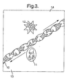
- FIG. 3 The appearance of a typical decoupled device is shown in Figure 3 in which the diffractive microstructure (holographic imagery) 10-12 is confined to patterned areas or domains that are opaquely metallised - the reflection filter acting as an iridescent background. Although not visible in Figure 3 , the background will exhibit different colours in the regions 13,14, the colours gradually merging when they meet.
- the diffractive microstructure holographic imagery
- These areas or domains 10-12 will have shapes which are aesthetically relevant to holographic imagery contained within them - they may be crests, logos, characters or elongated shapes through which moving patterns of diffracted light could progress.
- the decoupled device could be fabricated in several ways depending on the proposed application and composition of the reflection filter.
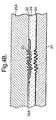
- the first way ( Figure 4A ) would be to first emboss the patterned areas of holographic imagery 20 into a 1-5 ⁇ m thick lacquer layer 21 of a holographic foil 26.
- the foil 26 also comprises a carrier 25, typically 12-25 ⁇ m thick polyester (PET), and a wax or silicone release layer 21A, typically 0.01-0.1 ⁇ m thick.
- An opaque metal coating 22A for example 20-50nm thick Al is then coated or applied to one or more selected regions, preferably in register with the microstructure 20, as shown. This can be achieved either by directly printing an oil mask prior to the metal coating or by applying the metal coating and the selectively demetallising.
- a semi-reflective coating 22, such as Cr, Ni or alloys such as Ni-chrome, 5-12 ⁇ m thick is applied.
- the complete area of the foil (on the microstructure side) is then successively coated, layer after layer to build up the desired thin film system 23.
- the dielectric layers may be metal oxides with thicknesses in the range 0.1-1 ⁇ m (preferably 0.2-0.5 ⁇ m) or acrylates (embossable) - typically these are created by flash evaporation of the monomer acrylate, followed by condensation onto the foil, followed by e-beam or UV curing. Suitable molecular weights for the monomer lie in the range 150-600 but especially 200-300. Thicknesses as for dielectrics.
- An example of a particular acrylate composition would be: Lauryl Monoacrylate 48.5% pbw Tricyclic hydrocarbon diacrylate 48.5% pbw Adhesion Promoters 30.0% pbw
- a fully reflective opaque metal layer 24 such as 30-50nm thick Al is then coated on the dielectric layer 23.
- a hot melt or pressure sensitive adhesive layer 27 is then coated on the layer 24 to a typical thickness of 0.5-20 ⁇ m.
- Figure 4B illustrates a modified form of the Figure 4A example in which the embossed lacquer layer is omitted, and the microstructure is embossed directly into the carrier 25A without an intermediate release layer.
- the carrier layer 25A is transparent to enable the device to be observed after it has been transferred on to a substrate.
- the carrier 25A may be 12-25 micron thick polyester but could also be polypropylene or PVC, with thicknesses in the range 10-60 ⁇ m.
- This structure is suitable for labels (with a pressure sensitive adhesive 27) or for threads with an optional heat activated adhesive.
- the remaining layers are provided in a similar manner to Figure 4A .
- an optional protective back coat could be provided between layers 24 and 27, particularly if the device will be used in a thread. This could be another UV curable acrylate provided in the same coating run as the layer 24.
- the second approach would be to take a prefabricated thin film system and coat it with an embossable lacquer and then repeat the above sequence of patterned embossing and demetallisation.
- the embossed lacquer is coated with a protective varnish (e.g. UV curing) and then finally laminated to a release coating carrier film (i.e. polyester) and adhesive coat.
- a protective varnish e.g. UV curing
- a release coating carrier film i.e. polyester
- the third approach would be simply to take the demetallised/pattern metallised embossed film (release coated carrier included if required) such as a therformable foil and laminate to it (using an optically clear adhesive) the prefabricated thin film system.
- the demetallised/pattern metallised embossed film release coated carrier included if required
- therformable foil and laminate to it (using an optically clear adhesive) the prefabricated thin film system.
- the monomer deposited acrylate layers described in CA-270113 are suitable.
- a therformable foil is embossed with the desired surface relief microstructure coated with one or more refractory (substantially transparent) layers, which may or may not be in register with the surface relief regions and then laminated to a thin film reflection filter structure.
- FIG. 5a illustrates an example of a decoupled system.
- a holographic foil 26 is embossed as in Figure 4A .
- the foil is provided with an additional protective coating 34 (which could also be used in Figure 4A ).
- This provides mechanical and chemical durability and is typically 1-5 ⁇ m thick.
- one or more reflective enhancing dielectric layers (only one shown in Figure 5A ) is applied. These layers could be coated in a spatially continuous manner over the entire area of the foil - or using masking techniques they could be applied/deposited over only the areas containing the holographic imaging or microstructure.
- a clear laminating adhesive layer 31 is coated onto the HRI layer 30, following which this structure is laminated to a previously fabricated reflection filter comprising a transparent, thin metal layer 32 of for example Cr or Ni, a thin film reflection filter layer 23, and an opaque metal layer 24. If required, an adhesive 27 is then applied. If desired, the HRI layer 30 can be confined to one or more regions between the microstructure 20 and the thin film reflection filter structure 23.
- Figure 5B illustrates a modification of the Figure 5A example, in which the microstructure 20 is embossed directly into the carrier 25B. In this case, the carrier 26 will not be removed from the device when it is transferred onto a substrate.
- Figure 5C illustrates another modification of Figure 5A in which the layer 30 is replaced by a discontinuous metal layer 50.
- the layer 50 is 30-50% demetallized.
- the layer 50 is registered with the microstructure 20 as well as having non-registered portions.
- Figure 6 illustrates a first example of a coupled system.
- a holographic foil 26 comprising a carrier 25 and release layer 21A, for example a hot stamping foil or a cold transfer foil, is used, and a protective coating 34, ideally composed of UV durable acrylate monomer is applied.
- a semi-reflective metal coating 22 is provided on the layer 34, the coating, as before, typically comprising 5-12nm thick chrome, Ni or alloy.
- a dielectric layer 23 is applied, this being a suitable UV curable acrylate monomer and then the dielectric layer 23 is coated with an opaque fully reflective metal layer 24, such as aluminium, having a thickness in the range of 30-50nm.
- This structure is then embossed with a surface relief microstructure 20 and finally an optional, adhesive coating 27 is applied, such as a hot melt or pressure sensitive adhesive.
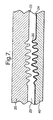
- Figure 7 is similar to the structure of Figure 6 , except that the release layer 21A and protective layer 34 are omitted, so that the carrier 25 will form part of the finished device. Further, the adhesive layer 27 is replaced by a protective coating 40, such as UV curable acrylate. This structure is suitable for use as a thread.
- Figure 8 illustrates a structure based on the Figure 6 example, and in which the layer 24 is patterned to match the microstructure regions 20.
Abstract
Description
- The invention relates to an optically variable security device for use, for example, for securing documents and articles against counterfeiting.
- The use of optical thin film structures to inhibit counterfeiting and illicit tampering is now a well established art. See for example
US-A-3858977 ,US-A-4721217 ,US-A-4930866 ,US-A-4994314 ,US-A-5009486 ,EP-A-0733919 and Dobrowolski, J.A, Ho, F.C., and Waldorf, A.J. "Research on Thin-Film Anticounterfeiting coatings at the National Research Council of Canada, Applied Optics, Vol 28, . These thin film structures often referred to as optical multilayers generally fall into two types; those which are purely dielectric and those which are composed of alternate dielectric (metal oxide or polymer) and metallic layers. The former has the advantage of being transparent and therefore suitable for over-laminate applications, however it requires a minimum of five layers to produce an iridescent device with acceptable luminosity and colour saturation (seen to best effect when located over a dark coloured substrate or background). Whereas the metallic combination functions well with only 3 layers and is therefore significantly cheaper to fabricate. However in both cases the iridescent quality of the multi-layer is strongly influenced by the deposition technology. - The optically variable effects produced by thin film devices, although attractive and distinctive, are fairly modest when compared to holograms and other diffraction based optically variable devices (DOVID's). For a full review of the various OVD technologies see "Optical Document Security", . Typically at a given viewing angle the observer will see the device replay one colour or hue, while tilting the device substantially within the plane of reflection will either increase or decrease the optical path length travelled by the light rays as they are reflected within the layers thereby causing the device to undergo a colour shift to a contrastingly different colour (in commercial examples a typical shift is from blue-green to gold or red to green) . Their appearance can be made more sophisticated by incorporating into them graphical design elements like logos and alphanumeric characters using techniques such as masking (during the vacuum deposition stage) or laser ablation to create voids within the layers, although these substantially add to the fabrication cost of the device and are limited in their scope. However in
CA-A-2,172, 113 where they teach the art of using UV or e-beam curable acrylate monomer technology to fabricate metallic reflection filters: various low cost non-vacuum methods are described to produce patterned changes in the thickness of the acrylate layer and therefore patterned areas of relative colour shift with the background or hue of the reflection filter. Though it should be said that a consideration of these methods strongly infers that only fairly coarse patterning is possible. In the case of iridescent metallic reflection filters the technique of producing demetallised shapes or indicia in the opaque metal layer, using a chemical etchant has also been used to produce more intricately patterned and therefore secure OVD's. - In accordance with a first aspect of the present invention, an optically variable security device comprises a thin film reflection filter structure, which exhibits a first optically variable effect; and a relief structure on or in the thin film reflection filter structure, which exhibits a second optically variable effect.
- In accordance with a second aspect of the present invention, a method of manufacturing an optically variable security device comprises providing a relief structure on or in a thin film reflection filter structure, the relief structure and the thin film reflection film structure exhibiting different first and second optically variable effects.
- We have devised a new security device which has a very characteristic appearance, and by virtue of combining two different technologies is inherently difficult to counterfeit. In preferred examples, an iridescent reflection filter based security device is patterned with graphical elements/areas containing surface relief structures often referred to in the art as an optical microstructure, preferably a diffractive or holographic microstructure - particularly as 1st order diffractive iridescence has a very different appearance to that produced by thin film interference (in the former, the colour shifts are non-specular and evolve much more rapidly with changes in viewing geometry). Also the diffractive microstructure within the patterned areas can be originated to exhibit clear kinegraphic or spatial movement effects on tipping or rotating the device.
- Now it should be appreciated that although thin film iridescence and diffraction are both interference phenomena, the former manifests this phenomena through amplitude division whereas the latter depends on the effect of wavefront division. This means the structures can be combined in two fundamentally different ways : the first way is to fabricate the security device such that the light it directs into the observer's eye has been subject to (and therefore conditioned by) both amplitude and wavefront division (coupled system) or to fabricate the device such that observed light has only been conditioned by either of these effects acting separately (de-coupled system).
- Consider
Figure 1 which shows for simplicity atransparent layer 1 sandwiched between asemi-transparent metal layer 2 and anopaque metal layer 3. Typically, thelayer 2 is a partially transparent metal coating, themiddle layer 1 is a dielectric (metal oxide or polymer) and thelayer 3 an opaque metal coating (usually A1). When a monochromatic beam oflight 4 is incident upon thefirst layer 2, its amplitude will be split or divided by partial reflection: the reflected wave front will propagate directly towards the observer whilst the second transmitted beam will travel an optical path length of 2ndcos Ør, where n is the refractive index of thelayer 1 before exiting the film and propagating towards the observer (it will also experience a double absorption on twice passing through the first metal layer 2). Clearly if the two wavefronts (or partial amplitudes) travelling towards the observer are to constructively interfere, thus enhancing the reflectivity of the thin film system at that wavelength, then the path difference between all corresponding points on the two wavefronts must equal some integer multiple, p, of the incident wavelength. - Now it can easily be shown that this optical path difference (OPD) is equal to 2nd cos Ør; therefore assuming there is the same reflective phase shift p at each interface then the condition for constructive interference is given by

- Conversely if the path difference OPD between the two wavefronts is equal to an odd multiple of half wavelengths (i.e. OPD = [ p +1/2 ] λ ) then they will destructively interfere -thus giving rise to reduced reflectance at that wavelength.
- If such a thin film structure is to effectively function as an iridescent reflection filter then we require two things: firstly that the effects of constructive and destructive interfence are optimised to achieve a high degree of luminosity and spectral selectivity. Secondly the peak reflective wavelength (i.e. the colour) of the thin film system should visibly change as the observer changes the viewing geometry by a convenient amount, i.e. it must exhibit clear colour shifts when the plane of the device is tipped by around 10 degrees within the plane of reflection (as defined by the light source and observer). The first condition requires that the amplitudes or intensities of the two reflected rays (5) and (6) are as large as possible (maximizes constructive interference) and ideally equal in amplitude so that they cancel each other when 180 degrees out of phase (complete destructive interference). Theoretically this requires that the metals used for the semi-transparent and
opaque metal coatings - With regard to colour shift, i.e. the rate at which the peak reflectance wavelength changes with observation geometry, this is proportional to the optical path difference and therefore the product nd - the larger this value the more rapidly the colour of the reflection filter changes with viewing angle. It should also be appreciated that as the thickness increases from say 100nm onwards (and assuming the refractive index of the dielectric layer to be 2.0), the device will initially function through first order interference (p=1). However at around 180-200nm the thin film structure supports both first order constructive interference at the red end of the spectrum and second order ( p=2 ) constructive interference at the blue end of the spectrum. We then have created a device which exhibits a red-orange to blue colour shift whereas a device permitting only first order interference will only exhibit continuous/gradual changes in colour, not a colour jump. If we take this further, and increase the layer thickness to around 350nm then the device will support both second and third order interference producing a red to green colour shift, which evolves more rapidly with angle than the preceding case.
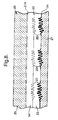
- Having outlined the fundamental design and manufacturing criteria for a metallic layer reflection filter we next consider the physics of coupling this system to a sinusoidal relief structure with a pitch of 1mm (see
Figure 2 ). Now the pitch of the relief structures that compose a security hologram or DOVID are normally designed or created such that the 1st order replay is approximately at right angles to the plane of the device when illuminated withwhite light 4. In practice this means holograms and other DOVIDs contain grating structures with periodicities ranging from 0.7. µm to 1.4. µm (hence the choice of 1 µm for inclusion inFigure 2 ). As regards the thickness d of the intermediate layer we choose this on the basis of previous discussion to be 0.2mm. - If we now consider rays incident at two different points, A and B, on the first (partially metallised)
interface 2. At each point we see that, as before, a fraction of the incident wavelet amplitude is directly diffracted/reflected into the observer's eye. It should be clear however from this scale drawing that this optical path is very different for the two points of incidence on the relief, i.e. the optical path at point A is twice that at point B. It therefore follows that if at some wavelength the partial amplitudes of the light ray diffracted from the upper and lower interface at point A are in phase, then those at point B may be near to being in antiphase and therefore cancel out. - Although to simplify the argument we chose two points of incidence on the relief profile that had markedly different path lengths, it is clear that for the periodicities that characterise most holograms or DOVIDs (less than 1.3um) the processes of diffraction (wavefront division) and thin film interference (amplitude division) will not in general couple efficiently together (i.e. the processes of constructive and destructive interference can never be optimised across all of the wavefront) leading to reduced luminosity and spectral selectivity.
- There will however be cases where it is desirable to suppress certain colours in the diffraction spectrum of a hologram/DOVID in which case the drawbacks of this coupled system become secondary. Also this coupled system tends to have the most direct fabrication routes: one route would be to first emboss the holographic foil with holographic image generating microstructure, preferably in defined or selected areas. This microstructure is then vacuum coated with first the semi-transparent metal coating, then the dielectric layer, then the opaque metal layer, then (optionally) a protective coating for increased chemical durability and finally an adhesive coat.
- However if the dielectric layer is composed of a UV cured acrylate, then we can take advantage of the fact that such a material is mechanically "non glassy" (i.e. ductile) and therefore embossable. We therefore fabricate our coupled device by, as before, first depositing a semi-reflective metal coating onto the carrier foil which depending on application may or may not be release coated. We next deposit our u.v. or e-beam cured/polymerised acrylate using the sequence of flash evaporation, condensation and u.v./e-beam irradiation described in
CA-A-2,172,113 and then emboss the holographic generating structure directly into the back surface of the reflection filter (with the opaque metal coating, generally aluminium, facing the embossing die or shim). Again a preferred embodiment would be to confine the microstructure to a pattern of selected areas such that the reflection is decoratively patterned with holographic microstructure. - We propose here further developing the above fabrication process by flash evaporating protective acrylic layers either before the deposition of the first semi-reflective metal coating or after the deposition of the final opaque reflective metal coating or in some cases both (though the former, acting as a protective overcoat is particularly pertinent to the case where carrier foil is simply a temporary substrate i.e. release layer present). In either case the molecular composition of the acrylate monomer can be adjusted to give the desired chemical or mechanical durability.
- Now it is known in the art (of vacuum coating science) that achieving optimal adhesion between two coatings requires that the structure remain under vacuum in between the respective coating stages. We therefore propose a refinement of the fabrication process in order to produce a more tamper evident iridescent device. Specifically this could be achieved in two ways: the simplest embodiment is to admit air into the vacuum chamber (i.e "breaking the vacuum") between the deposition of the first semi-transparent metal coating and the deposition of the dielectric layer or coating. Alternatively a molecular species can be introduced into the vacuum which adsorbs on to the surface of the first coating and then a second coating is deposited. We thereby creating a weak interface between the two coatings. Therefore in an attempt to remove the security device from the article it is protecting, this weak layer will fail before the adhesive and in failing irreparably and obviously change the appearance of the device.
- Finally in relation to the coupled device we have assumed that the opaque metal coating is continuous - however we could modify the fabrication stage such that this layer was spatially pattern metallised to create transparent decorative shapes, meaningful forms of indicia (e.g. letters, numbers) or a halftone pattern of transparent dots. The fabrication of this discontinuous metal coating could be effected in a number of ways: one method would be to print an oil mask on to the dielectric layer before vacuum coating the metal layer (the metal would adhere only to the oil-free areas). A second method would be to print an etchant directly onto the back of the metal (in the case of aluminium, a suitable etchant would be sodium hydroxide). Alternatively a third method would be to print an etchant resistant mask on to back of the aluminium before uniformly coating with etchant. Note in methods two and three a final wash off stage will be required to remove etchant and dissolved metal.
- So far we have proposed ways of fabricating coupled devices which redirect into the observers eye only that light which has been subject to the combined effect of the two iridescence generating structures (e.g. surface relief microstructure and thin film reflection filter). However as we have alluded to earlier their may be many cases where it is for example desirable to observe the full diffractive rainbow spectrum of the holographic generating structure, in which case we need to decouple the two iridescence generating mechanisms. Herein we propose two distinct approaches or arrangements for achieving this: in the first arrangement, one or more opaque regions, typically achieved through metallisation, may be provided between the holographic image generating structure and the thin film reflection filter structure. This provides a way of shielding the relief structure from the thin film reflection filter so that the holographic image can be viewed, despite the presence of the thin film reflection filter structure.
- Advantage can be taken of the presence of the opaque regions, to design them in predetermined shapes. In some examples each region may define one or more of a crest, logo, character or indicia, or a, preferably elongate, shape through which moving patterns of diffractive light progress.
- In another arrangement, one or more layers/coatings are provided between the holographic image generating structure and the thin film reflection filter that are substantially transparent. These would include one or more high refractory layers (dielectric or semiconductor) and one adhesive layer (preferably of high optical clarity). The refractory layer or layers should be composed (i.e. have the relative refractive indices and coating thicknesses) in such a way as to enhance the reflectivity or luminosity of the holographic image generating structure.
- As with the opaque layers mentioned above, the additional layers or coatings can be confined to only those areas that contain holographic image generating structure and typically may be in the form of crests, logos and the like as mentioned above in connection with opaque layers.
- So far we have made the assumption that the diffractive microstructure supports devices that are viewed in the first diffracted order. However, the above fabrication methods could equally apply to zero order diffraction devices (ZODs). These are devices in which the periodicity of the relief is around 0.4µm or less so that for visible light no first order diffractive effects exist at normal incidence illumination. The preferred shape of the relief is rectangular and the depth of the relief is ideally greater than or equal to the pitch. For a thorough review of the characteristics of these devices and their role in optical security, the reader is referred to Gale, M.T., Knop, K.., and Morf, R., "Zero-order diffractive microstructures for security applications" SPIE vol.1210 Optical Security and Anticounterfeiting Systems, Los Angeles 1990, pp83-89 and more recently in
chapter 12 of the publication "Optical Document Security" by R.L.van Renesse. What is relevant to this discussion is that their iridescence is superficially similar in appearance to conventional reflection filters with one significant difference, which is that their specular (i.e. zero order) reflection is rotationally variable. - Specifically rotation of the microstructure in its own plane leads to a major change in colour. For example, when the grating grooves lie at right angles to the plane of reflection (the normal viewing mode) the device may have been designed to appear green. When, however, the ZOD is rotated such that grooves lie in the plane of reflection the device will appear brown in hue. We herein propose combining this contrasting rotational behaviour between a ZOD and a thin film interference reflection filter with our general theme of confining the microstructure to selected areas or regions that our superposed over the reflection filter (e.g. patterning the reflection filter with microstructure) to create a new security device, which both in terms of optical variability and decorative effect, has a differential appearance.
- An example of one possible embodiment would be to compose the device such that for one orientation, the ZOD (microstructure grooves at right angles to the plane of reflection) and the reflection filter have been designed to reflect green/blue light and no decorative patterning will be evident; however on rotation by 90 degrees the ZOD areas will reveal themselves as a patterned areas of brown colour shift on a green/blue background. In other examples the patterning of the reflection filter with areas of ZOD microstructure can be made more visually complex by changing the orientation or pitch of the ZOD microstructure from area to area. Indeed in a further refinement within each of the selected areas the orientation/pitch of the ZOD microstructure can be modified to create a zero-order image within each area.
- We have already discussed the limitation, that for the 1 µm grating periodicity typical of a hologram/DOVID, multilayer enhancement is ineffective, degrading both the thin film interference and diffractive effects. However, at significantly longer periodicities such as 3 µm or more it can be shown graphically that every point on the wavefront travels a near equal (double pass) optical path length within the film. In other words a reflection filter will function efficiently when applied or conforming to relief structures with a periodicity ≥ 3 µm. Now if these relief structure are fabricated to be triangular profiles, and if they have a periodicity of 5 µm or more, then they will start to exhibit refractive/reflective characteristics as well as diffractive i.e. they will function as lenticular microprisms or micromirrors. We therefore propose directly embossing decoratively and securely patterned areas of this relief structure into a metal/polymer reflection filter - although direct deposition could also be use for "glassy, non-embossable dielectrics".
- It should be appreciated that the effect of impressing the think film structure with the profile of these coarse microprisms/micromirros will be to locally change the specular normal and therefore colour replayed by the thin film structure. We would therefore have a security device consisting of an iridescent reflection filter which at one orientation will be decoratively patterned with areas of a different iridescent hue or colour) prism grooves perpendicular to axis of reflection). When the observer rotates the device by 90 degrees these patterned areas will progressively transform into the same colour as the background (prism/grooves along axis of reflection).
- It is well known that the random surface relief created by holographically recording the speckle irradiances pattern generated by a suitable diffusing screen, will in turn, when embossed into metallised foil produce reflective diffuser with a whitish hue.
- In another example, therefore, we provide a device in which an iridescent reflection filter is decoratively and intricately patterned (e.g. with logos, text, microtext etc.) with areas of random diffuse microstructure. This can be most simply achieved by directly embossing into a metal/polymer thin film system. The random microstructure will substantially suppress the specular iridescence created by the thin film structure and ideally replace it with one, which has a distinctive whitish hue.
- The security device can be used on a wide variety of documents and articles including visas, passports, licences, cheques, identity cards, plastic cards, bank notes, tickets, bonds, share certificates, vouchers, passes, permits, electrostatic photocopies electrostatic laser printed materials, brand authentication labels, serial numbering slips, quality control certificates, bills of lading and other shipping documentation, legal documents and tamper evident labels. It can also be used in embedded features such as security threads.
- Some examples of security devices and methods according to the invention will now be described with reference to the accompanying drawings, in which:-
-
Figures 1 and 2 are schematic, cross-sections through devices to show the problems of combining thin film reflection filters with surface relief holographic image generating structures; -
Figure 3 is a plan of an example of a security device according to the invention; -
Figures 4A ,4B ,5A ,5B and5C are schematic cross-sections through first to fifth examples of decoupled security devices according to the invention; and, -
Figures 6 to 8 are schematic cross-sections through sixth to eighth examples of coupled security devices according to the invention. - The appearance of a typical decoupled device is shown in
Figure 3 in which the diffractive microstructure (holographic imagery) 10-12 is confined to patterned areas or domains that are opaquely metallised - the reflection filter acting as an iridescent background. Although not visible inFigure 3 , the background will exhibit different colours in theregions - These areas or domains 10-12 will have shapes which are aesthetically relevant to holographic imagery contained within them - they may be crests, logos, characters or elongated shapes through which moving patterns of diffracted light could progress.
- This decoupled device could be fabricated in several ways depending on the proposed application and composition of the reflection filter. The first way (
Figure 4A ) would be to first emboss the patterned areas ofholographic imagery 20 into a 1-5µmthick lacquer layer 21 of aholographic foil 26. Thefoil 26 also comprises acarrier 25, typically 12-25µm thick polyester (PET), and a wax orsilicone release layer 21A, typically 0.01-0.1µm thick. - An
opaque metal coating 22A, for example 20-50nm thick Al is then coated or applied to one or more selected regions, preferably in register with themicrostructure 20, as shown. This can be achieved either by directly printing an oil mask prior to the metal coating or by applying the metal coating and the selectively demetallising. - Next a
semi-reflective coating 22, such as Cr, Ni or alloys such as Ni-chrome, 5-12µm thick is applied. - The complete area of the foil (on the microstructure side) is then successively coated, layer after layer to build up the desired
thin film system 23. The dielectric layers may be metal oxides with thicknesses in the range 0.1-1µm (preferably 0.2-0.5µm) or acrylates (embossable) - typically these are created by flash evaporation of the monomer acrylate, followed by condensation onto the foil, followed by e-beam or UV curing. Suitable molecular weights for the monomer lie in the range 150-600 but especially 200-300. Thicknesses as for dielectrics. An example of a particular acrylate composition would be:Lauryl Monoacrylate 48.5% pbw Tricyclic hydrocarbon diacrylate 48.5% pbw Adhesion Promoters 30.0% pbw - A fully reflective
opaque metal layer 24 such as 30-50nm thick Al is then coated on thedielectric layer 23. A hot melt or pressure sensitiveadhesive layer 27 is then coated on thelayer 24 to a typical thickness of 0.5-20µm. - The materials and thicknesses mentioned above are also applicable to the examples to be described below where the same reference numerals are used to identify similar layers.
-
Figure 4B illustrates a modified form of theFigure 4A example in which the embossed lacquer layer is omitted, and the microstructure is embossed directly into thecarrier 25A without an intermediate release layer. In this case, thecarrier layer 25A is transparent to enable the device to be observed after it has been transferred on to a substrate. Thecarrier 25A may be 12-25 micron thick polyester but could also be polypropylene or PVC, with thicknesses in the range 10-60µm. This structure is suitable for labels (with a pressure sensitive adhesive 27) or for threads with an optional heat activated adhesive. The remaining layers are provided in a similar manner toFigure 4A . However, an optional protective back coat could be provided betweenlayers layer 24. - The second approach would be to take a prefabricated thin film system and coat it with an embossable lacquer and then repeat the above sequence of patterned embossing and demetallisation. Next, the embossed lacquer is coated with a protective varnish (e.g. UV curing) and then finally laminated to a release coating carrier film (i.e. polyester) and adhesive coat.
- The third approach would be simply to take the demetallised/pattern metallised embossed film (release coated carrier included if required) such as a therformable foil and laminate to it (using an optically clear adhesive) the prefabricated thin film system. For the layer 23A, the monomer deposited acrylate layers described in
CA-270113 are suitable. - In a further example, a therformable foil is embossed with the desired surface relief microstructure coated with one or more refractory (substantially transparent) layers, which may or may not be in register with the surface relief regions and then laminated to a thin film reflection filter structure.
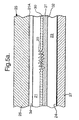
- In the examples described above, an
opaque metal layer 22A is provided between the microstructure and the thinfilm reflection structure 23.Figure 5a illustrates an example of a decoupled system. Aholographic foil 26 is embossed as inFigure 4A . In this case, the foil is provided with an additional protective coating 34 (which could also be used inFigure 4A ). This provides mechanical and chemical durability and is typically 1-5µm thick. Next one or more reflective enhancing dielectric layers (only one shown inFigure 5A ) is applied. These layers could be coated in a spatially continuous manner over the entire area of the foil - or using masking techniques they could be applied/deposited over only the areas containing the holographic imaging or microstructure. A clear laminatingadhesive layer 31 is coated onto theHRI layer 30, following which this structure is laminated to a previously fabricated reflection filter comprising a transparent,thin metal layer 32 of for example Cr or Ni, a thin filmreflection filter layer 23, and anopaque metal layer 24. If required, an adhesive 27 is then applied. If desired, theHRI layer 30 can be confined to one or more regions between themicrostructure 20 and the thin filmreflection filter structure 23. -
Figure 5B illustrates a modification of theFigure 5A example, in which themicrostructure 20 is embossed directly into the carrier 25B. In this case, thecarrier 26 will not be removed from the device when it is transferred onto a substrate. -
Figure 5C illustrates another modification ofFigure 5A in which thelayer 30 is replaced by adiscontinuous metal layer 50. In the preferred example, thelayer 50 is 30-50% demetallized. As can be seen, thelayer 50 is registered with themicrostructure 20 as well as having non-registered portions. - The examples described above are all decoupled systems.
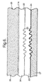
Figure 6 illustrates a first example of a coupled system. In this example, aholographic foil 26 comprising acarrier 25 andrelease layer 21A, for example a hot stamping foil or a cold transfer foil, is used, and aprotective coating 34, ideally composed of UV durable acrylate monomer is applied. Next asemi-reflective metal coating 22 is provided on thelayer 34, the coating, as before, typically comprising 5-12nm thick chrome, Ni or alloy. - A
dielectric layer 23 is applied, this being a suitable UV curable acrylate monomer and then thedielectric layer 23 is coated with an opaque fullyreflective metal layer 24, such as aluminium, having a thickness in the range of 30-50nm. This structure is then embossed with asurface relief microstructure 20 and finally an optional,adhesive coating 27 is applied, such as a hot melt or pressure sensitive adhesive. -
Figure 7 is similar to the structure ofFigure 6 , except that therelease layer 21A andprotective layer 34 are omitted, so that thecarrier 25 will form part of the finished device. Further, theadhesive layer 27 is replaced by aprotective coating 40, such as UV curable acrylate. This structure is suitable for use as a thread. - Finally,
Figure 8 illustrates a structure based on theFigure 6 example, and in which thelayer 24 is patterned to match themicrostructure regions 20.
Claims (15)
- An optically variable security device comprising a thin film reflection filter structure which exhibits a first optically variable effect; and a relief structure on or in the thin film reflection filter structure which exhibits a second optically variable effect, the relief structure having a periodicity of at least 3µm.
- A device according to claim 1, wherein the relief structure is a microstructure.
- A device according to claim 2, wherein the relief structure is a holographic image generating structure.
- A device according to claim 1, wherein the relief structure has a periodicity substantially greater than the (dielectric) layer or layers within the film structure, such that the thin film structure functions as a flat planar device.
- A device according to claim 4, wherein the relief structure functions as a set of lenticular microprisms or micromirrors.
- A device according to any of the preceding claims, wherein the periodicity is at least 5µm.
- A device according to any of the preceding claims, wherein the relief structure has a triangular profile.
- A device according to any of the preceding claims, wherein the thin film reflection filter comprises one or more dielectric layers and a reflective layer.
- A method of manufacturing an optically variable security device, the method comprising providing a relief structure on or in a thin film reflection filter structure, the relief structure and the thin film reflection filter structure exhibiting different first and second optically variable effects, and wherein the relief structure has a periodicity of at least 3µm.
- A method according to claim 9, wherein the relief structure is a microstructure.
- A method according to claim 10, wherein the relief structure is a holographic image generating structure.
- A method according to claim 9, wherein the relief structure has a periodicity substantially greater than the (dielectric) layer or layers within the film structure, such that the thin film structure functions as a flat planar device.
- A method according to claim 12, wherein the relief structure functions as a set of lenticular microprisms or micromirrors.
- A method according to any of claims 9 to 13, wherein the periodicity is at least 5µm.
- A method according to any of claims 9 to 14, wherein the relief structure has a triangular profile.
Applications Claiming Priority (2)
| Application Number | Priority Date | Filing Date | Title |
|---|---|---|---|
| GBGB0015873.3A GB0015873D0 (en) | 2000-06-28 | 2000-06-28 | Optically variable security device |
| EP01943671.6A EP1294575B1 (en) | 2000-06-28 | 2001-06-27 | Optically variable security device with a relief structure and with a thin film reflection filter and a method for its manufacture |
Related Parent Applications (3)
| Application Number | Title | Priority Date | Filing Date |
|---|---|---|---|
| EP01943671.6A Division-Into EP1294575B1 (en) | 2000-06-28 | 2001-06-27 | Optically variable security device with a relief structure and with a thin film reflection filter and a method for its manufacture |
| EP01943671.6A Division EP1294575B1 (en) | 2000-06-28 | 2001-06-27 | Optically variable security device with a relief structure and with a thin film reflection filter and a method for its manufacture |
| EP01943671.6 Division | 2001-06-27 |
Publications (3)
| Publication Number | Publication Date |
|---|---|
| EP2390106A2 true EP2390106A2 (en) | 2011-11-30 |
| EP2390106A3 EP2390106A3 (en) | 2011-12-21 |
| EP2390106B1 EP2390106B1 (en) | 2018-01-17 |
Family
ID=9894605
Family Applications (2)
| Application Number | Title | Priority Date | Filing Date |
|---|---|---|---|
| EP01943671.6A Revoked EP1294575B1 (en) | 2000-06-28 | 2001-06-27 | Optically variable security device with a relief structure and with a thin film reflection filter and a method for its manufacture |
| EP11174009.8A Expired - Lifetime EP2390106B1 (en) | 2000-06-28 | 2001-06-27 | Optically variable security devices, each with a relief structure and with a thin film reflection filter, and methods for their manufacture |
Family Applications Before (1)
| Application Number | Title | Priority Date | Filing Date |
|---|---|---|---|
| EP01943671.6A Revoked EP1294575B1 (en) | 2000-06-28 | 2001-06-27 | Optically variable security device with a relief structure and with a thin film reflection filter and a method for its manufacture |
Country Status (7)
| Country | Link |
|---|---|
| US (1) | US7054042B2 (en) |
| EP (2) | EP1294575B1 (en) |
| AU (1) | AU2001266209A1 (en) |
| CA (1) | CA2402134C (en) |
| CZ (1) | CZ299338B6 (en) |
| GB (1) | GB0015873D0 (en) |
| WO (1) | WO2002000445A1 (en) |
Cited By (4)
| Publication number | Priority date | Publication date | Assignee | Title |
|---|---|---|---|---|
| CN106573488A (en) * | 2014-09-03 | 2017-04-19 | 德国捷德有限公司 | Visually variable security element |
| WO2019219237A1 (en) | 2018-05-18 | 2019-11-21 | Giesecke+Devrient Currency Technology Gmbh | Optically variable security element having reflective area |
| EP3800063A1 (en) * | 2019-10-03 | 2021-04-07 | Hueck Folien Gesellschaft m.b.H. | Security element for securities or security papers |
| DE102020006902A1 (en) | 2020-11-10 | 2022-05-12 | Giesecke+Devrient Currency Technology Gmbh | Optically variable security element and method for producing an optically variable security element |
Families Citing this family (104)
| Publication number | Priority date | Publication date | Assignee | Title |
|---|---|---|---|---|
| US20070195392A1 (en) * | 1999-07-08 | 2007-08-23 | Jds Uniphase Corporation | Adhesive Chromagram And Method Of Forming Thereof |
| US7047883B2 (en) | 2002-07-15 | 2006-05-23 | Jds Uniphase Corporation | Method and apparatus for orienting magnetic flakes |
| US6761959B1 (en) * | 1999-07-08 | 2004-07-13 | Flex Products, Inc. | Diffractive surfaces with color shifting backgrounds |
| US7667895B2 (en) * | 1999-07-08 | 2010-02-23 | Jds Uniphase Corporation | Patterned structures with optically variable effects |
| US6987590B2 (en) * | 2003-09-18 | 2006-01-17 | Jds Uniphase Corporation | Patterned reflective optical structures |
| US11768321B2 (en) | 2000-01-21 | 2023-09-26 | Viavi Solutions Inc. | Optically variable security devices |
| WO2001053113A1 (en) * | 2000-01-21 | 2001-07-26 | Flex Products, Inc. | Optically variable security devices |
| US7625632B2 (en) * | 2002-07-15 | 2009-12-01 | Jds Uniphase Corporation | Alignable diffractive pigment flakes and method and apparatus for alignment and images formed therefrom |
| DE10150293B4 (en) * | 2001-10-12 | 2005-05-12 | Ovd Kinegram Ag | security element |
| WO2003053972A1 (en) * | 2001-12-20 | 2003-07-03 | Pharmacia & Upjohn Company | Pyridoquinoxaline antivirals |
| DE10226114A1 (en) * | 2001-12-21 | 2003-07-03 | Giesecke & Devrient Gmbh | Security element for security papers and documents of value |
| DE10163381A1 (en) | 2001-12-21 | 2003-07-03 | Giesecke & Devrient Gmbh | Security paper and method and device for its production |
| US7221512B2 (en) * | 2002-01-24 | 2007-05-22 | Nanoventions, Inc. | Light control material for displaying color information, and images |
| DE10207622A1 (en) † | 2002-02-22 | 2003-09-04 | Giesecke & Devrient Gmbh | Security document and security element for a security document |
| AU2003224248B2 (en) * | 2002-04-03 | 2006-01-19 | De La Rue International Limited | Optically variable security device |
| GB0207750D0 (en) * | 2002-04-03 | 2002-05-15 | Rue De Int Ltd | Optically variable security device and method |
| DE10216562C1 (en) * | 2002-04-05 | 2003-12-11 | Ovd Kinegram Ag Zug | Security element with micro and macro structures |
| US6982832B2 (en) | 2002-05-14 | 2006-01-03 | Leonard Kurz Gmbh & Co. Kg | Optically variable element comprising a sequence of thin-film layers |
| ATE534531T1 (en) | 2002-05-14 | 2011-12-15 | Leonhard Kurz Stiftung & Co Kg | OPTICALLY VARIABLE ELEMENT WITH PARTIAL TRANSPARENT ELEMENT |
| DE10222433A1 (en) * | 2002-05-22 | 2003-12-11 | Kurz Leonhard Fa | Strip-shaped security element |
| US11230127B2 (en) | 2002-07-15 | 2022-01-25 | Viavi Solutions Inc. | Method and apparatus for orienting magnetic flakes |
| US7934451B2 (en) * | 2002-07-15 | 2011-05-03 | Jds Uniphase Corporation | Apparatus for orienting magnetic flakes |
| DE10232245B4 (en) | 2002-07-17 | 2008-06-12 | Leonhard Kurz Gmbh & Co. Kg | Optically variable element with varying spacer layer thickness |
| AT413360B (en) | 2002-08-06 | 2006-02-15 | Hueck Folien Gmbh | METHOD FOR PRODUCING FAKE-SECURE IDENTIFICATION FEATURES |
| US8025952B2 (en) * | 2002-09-13 | 2011-09-27 | Jds Uniphase Corporation | Printed magnetic ink overt security image |
| US9164575B2 (en) * | 2002-09-13 | 2015-10-20 | Jds Uniphase Corporation | Provision of frames or borders around pigment flakes for covert security applications |
| US7645510B2 (en) * | 2002-09-13 | 2010-01-12 | Jds Uniphase Corporation | Provision of frames or borders around opaque flakes for covert security applications |
| US9458324B2 (en) | 2002-09-13 | 2016-10-04 | Viava Solutions Inc. | Flakes with undulate borders and method of forming thereof |
| US7674501B2 (en) * | 2002-09-13 | 2010-03-09 | Jds Uniphase Corporation | Two-step method of coating an article for security printing by application of electric or magnetic field |
| DE10254500B4 (en) * | 2002-11-22 | 2006-03-16 | Ovd Kinegram Ag | Optically variable element and its use |
| US20040099740A1 (en) * | 2002-11-25 | 2004-05-27 | Chresand Thomas J. | Merchandising components for authenticating products, and combinations and methods utilizing the same |
| US20040229065A1 (en) * | 2003-02-28 | 2004-11-18 | Toray Plastics (America), Inc. | High refractive index coated embossable film |
| FR2856339B1 (en) * | 2003-06-23 | 2006-05-26 | Banque De France | SECURITY BAND FOR DOCUMENTATION AND SECURE DOCUMENT |
| CN1597334B (en) | 2003-07-14 | 2011-03-30 | Jds尤尼费斯公司 | Counterfeiting line and method for manufacturing optical variable device |
| US20080019003A1 (en) * | 2003-07-14 | 2008-01-24 | Jds Uniphase Corporation | Vacuum Roll Coated Security Thin Film Interference Products With Overt And/Or Covert Patterned Layers |
| US7550197B2 (en) * | 2003-08-14 | 2009-06-23 | Jds Uniphase Corporation | Non-toxic flakes for authentication of pharmaceutical articles |
| DE102004016596B4 (en) | 2004-04-03 | 2006-07-27 | Ovd Kinegram Ag | Security element in the form of a multilayer film body and method for producing a security element |
| US7157135B2 (en) * | 2004-06-09 | 2007-01-02 | Toray Plastics (America), Inc. | Co-extruded high refractive index coated embossable film |
| EP1771758A2 (en) * | 2004-07-26 | 2007-04-11 | Applied Opsec, Inc. | Diffraction-based optical grating structure and method of creating the same |
| GB0417422D0 (en) * | 2004-08-05 | 2004-09-08 | Suisse Electronique Microtech | Security device |
| GB0422266D0 (en) * | 2004-10-07 | 2004-11-10 | Suisse Electronique Microtech | Security device |
| EP1652688A1 (en) | 2004-10-29 | 2006-05-03 | Arjowiggins Security | Security device |
| US7616332B2 (en) | 2004-12-02 | 2009-11-10 | 3M Innovative Properties Company | System for reading and authenticating a composite image in a sheeting |
| DE102004059798A1 (en) | 2004-12-10 | 2006-06-29 | Ovd Kinegram Ag | Optically variable element with electrically active layer |
| TWI402106B (en) * | 2005-04-06 | 2013-07-21 | Jds Uniphase Corp | Dynamic appearance-changing optical devices (dacod) printed in a shaped magnetic field including printable fresnel structures |
| DE102005017169B4 (en) * | 2005-04-13 | 2023-06-22 | Ovd Kinegram Ag | transfer film |
| US20070098959A1 (en) * | 2005-06-03 | 2007-05-03 | Daniel Lieberman | Substrates and articles having selective printed surface reliefs |
| US20060275625A1 (en) * | 2005-06-03 | 2006-12-07 | Daniel Lieberman | High and low refractive index and metallic surface relief coatings |
| AU2006202315B2 (en) * | 2005-06-17 | 2011-01-27 | Viavi Solutions Inc. | Covert security coating |
| DE602005025879D1 (en) * | 2005-09-26 | 2011-02-24 | Suisse Electronique Microtech | A diffractive security element |
| CA2564764C (en) * | 2005-10-25 | 2014-05-13 | Jds Uniphase Corporation | Patterned optical structures with enhanced security feature |
| AU2006249295A1 (en) * | 2005-12-15 | 2007-07-05 | Jds Uniphase Corporation | Security device with metameric features using diffractive pigment flakes |
| DE102005061749A1 (en) † | 2005-12-21 | 2007-07-05 | Giesecke & Devrient Gmbh | Optically variable security element for making valuable objects safe has an achromatic reflecting micro-structure taking the form of a mosaic made from achromatic reflecting mosaic elements |
| EP1977399A4 (en) * | 2006-01-16 | 2010-09-01 | Securency Int Pty Ltd | Data storage in a diffractive optical element |
| CA2580321C (en) * | 2006-03-06 | 2014-11-04 | Jds Uniphase Corporation | Security devices incorporating optically variable adhesive |
| KR101428956B1 (en) * | 2006-04-12 | 2014-08-12 | 도요세이칸 그룹 홀딩스 가부시키가이샤 | Structure, forming method of structure, structure forming device, structure color and/or diffraction light reading method, and truth/false discriminating method |
| RU2443004C2 (en) * | 2006-05-02 | 2012-02-20 | Холограм Индастрис | Optical security marking component, method of manufacturing such a component, system comprising such a component, and reader for checking such a component |
| EP1854642B1 (en) | 2006-05-12 | 2015-05-27 | JDS Uniphase Corporation | A security device formed by a hologram and a color shifting ink |
| CA2592667C (en) * | 2006-07-12 | 2014-05-13 | Jds Uniphase Corporation | Stamping a coating of cured field aligned special effect flakes and image formed thereby |
| US7835047B1 (en) * | 2006-07-13 | 2010-11-16 | Raiford Frank D | Bi-directional informational article within an optical variable devise |
| US7800825B2 (en) * | 2006-12-04 | 2010-09-21 | 3M Innovative Properties Company | User interface including composite images that float |
| DE102007039996B4 (en) * | 2007-02-07 | 2020-09-24 | Leonhard Kurz Stiftung & Co. Kg | Security element for a security document and method for its production |
| BE1017460A6 (en) * | 2007-02-09 | 2008-10-07 | Leo Vermeulen Consulting Lvc | LENTICULAR FOIL. |
| FI2165224T3 (en) | 2007-07-11 | 2024-01-11 | Thales Dis France Sas | Sheeting with composite image that floats |
| DE102007034716A1 (en) † | 2007-07-23 | 2009-01-29 | Giesecke & Devrient Gmbh | security element |
| AU2008301524B2 (en) * | 2007-09-20 | 2011-11-10 | Toppan Printing Co., Ltd. | Optical device, laminate and labelled article |
| US8586285B2 (en) * | 2007-11-27 | 2013-11-19 | 3M Innovative Properties Company | Methods for forming sheeting with a composite image that floats and a master tooling |
| DE102007061828A1 (en) | 2007-12-20 | 2009-06-25 | Giesecke & Devrient Gmbh | Security element and method for its production |
| DE102007061827A1 (en) | 2007-12-20 | 2009-06-25 | Giesecke & Devrient Gmbh | Security element and method for its production |
| DE102008005019B4 (en) | 2008-01-17 | 2010-08-05 | Ovd Kinegram Ag | Foil element and the use of this foil element |
| AU2008348659B2 (en) * | 2008-01-23 | 2014-04-03 | Opsec Security Group Inc. | Optically variable magnetic stripe assembly |
| JP2009193069A (en) | 2008-02-13 | 2009-08-27 | Jds Uniphase Corp | Medium for laser printing including optical special effect flake |
| DE102008009296A1 (en) | 2008-02-15 | 2009-08-20 | Giesecke & Devrient Gmbh | Security element and method for its production |
| DE102008013167A1 (en) * | 2008-03-07 | 2009-09-10 | Giesecke & Devrient Gmbh | Security element and method for its production |
| EP2161598B2 (en) | 2008-09-05 | 2021-06-09 | Viavi Solutions Inc. | An Optical Device Exhibiting Color Shift upon Rotation |
| US7995278B2 (en) * | 2008-10-23 | 2011-08-09 | 3M Innovative Properties Company | Methods of forming sheeting with composite images that float and sheeting with composite images that float |
| US8111463B2 (en) | 2008-10-23 | 2012-02-07 | 3M Innovative Properties Company | Methods of forming sheeting with composite images that float and sheeting with composite images that float |
| AT507647B1 (en) * | 2008-12-11 | 2011-06-15 | Hueck Folien Gmbh | TRANSPARENT SAFETY ELEMENT |
| ES2345651B2 (en) | 2009-03-27 | 2011-05-17 | Universidad Politecnica De Valencia | OPTICAL SECURITY BRAND THAT INCLUDES METAMATERIALS WITH MAGNETIC RESPONSE, AUTHENTICATION PROCEDURE USING THE BRAND AND USE OF THE MARK APPLIED IN AN ARTICLE. |
| EP2267686B1 (en) * | 2009-05-07 | 2013-11-20 | Hueck Folien Ges.m.b.H. | Safety label with authenticity and manipulation evidence |
| EP2264491B1 (en) * | 2009-06-15 | 2017-08-09 | CSEM Centre Suisse d'Electronique et de Microtechnique SA - Recherche et Développement | Zero-order diffractive filter and method for manufacturing thereof |
| DE102009041583A1 (en) | 2009-09-15 | 2011-03-17 | Giesecke & Devrient Gmbh | Thin-film element with interference layer structure |
| US20100194093A1 (en) * | 2009-12-23 | 2010-08-05 | Bank Of Canada | Security devices, their production and use |
| JP2011158788A (en) * | 2010-02-02 | 2011-08-18 | Sony Corp | Hologram-including medium, apparatus for producing hologram-including medium, and information authentication method |
| KR101662320B1 (en) * | 2010-04-15 | 2016-10-11 | 삼성전자주식회사 | Dual surface treated injection molding article and manufacturing method thereof |
| WO2012059861A1 (en) * | 2010-11-02 | 2012-05-10 | Kba-Notasys Sa | Device for irradiating substrate material in the form of a sheet or web and uses thereof |
| DE102010050895A1 (en) * | 2010-11-10 | 2012-05-10 | Giesecke & Devrient Gmbh | Thin-film element with multilayer structure |
| JP5929013B2 (en) | 2011-05-25 | 2016-06-01 | 凸版印刷株式会社 | Colored anti-counterfeit structure and colored anti-counterfeit medium |
| EP2538247B1 (en) | 2011-06-23 | 2018-04-11 | Viavi Solutions Inc. | Multi color-shifting security devices |
| RU2016144474A (en) | 2011-09-26 | 2018-12-18 | Крейн Секьюрити Текнолоджис, Инк. | METHOD FOR PRODUCING COMPOSITE TAPE AND PROTECTIVE PRODUCTS EXECUTED FROM COMPOSITE TAPE |
| WO2013065871A1 (en) * | 2011-11-02 | 2013-05-10 | Canon Kabushiki Kaisha | Recorded matter, recording method, and image processing method |
| ES2703755T3 (en) | 2012-01-12 | 2019-03-12 | Viavi Solutions Inc | Article with curved patterns formed by aligned pigment flakes |
| GB201301788D0 (en) * | 2013-02-01 | 2013-03-20 | Rue De Int Ltd | Security devices and methods of manufacture thereof |
| GB2510381B (en) | 2013-02-01 | 2015-11-04 | Rue De Int Ltd | Security devices and methods of manufacture thereof |
| GB201301790D0 (en) * | 2013-02-01 | 2013-03-20 | Rue De Int Ltd | Security devices and methods of manufacture thereof |
| US9110442B1 (en) | 2013-03-15 | 2015-08-18 | Frank D. Raiford | Information article having populated and laser ablated indicia in registration |
| KR20160024872A (en) * | 2013-06-27 | 2016-03-07 | 피코순 오와이 | Anti-counterfeit signature |
| GB201400910D0 (en) | 2014-01-20 | 2014-03-05 | Rue De Int Ltd | Security elements and methods of their manufacture |
| US9489604B2 (en) | 2014-06-03 | 2016-11-08 | IE-9 Technology Corp. | Optically variable data storage device |
| US11126902B2 (en) | 2014-06-03 | 2021-09-21 | IE-9 Technology Corp. | Optically variable data storage device |
| GB2555491B (en) | 2016-11-01 | 2019-03-27 | De La Rue Int Ltd | Security devices and methods of manufacture thereof |
| DE102017130588A1 (en) * | 2017-12-19 | 2019-06-19 | Giesecke+Devrient Currency Technology Gmbh | value document |
| CN108388060B (en) * | 2018-03-13 | 2022-05-13 | 京东方科技集团股份有限公司 | Light-emitting display substrate, display panel, control method of display panel and display device |
| WO2020122952A1 (en) * | 2018-12-14 | 2020-06-18 | Lawrence Livermore National Security, Llc | Directionally dependent optical features apparatus and method |
Citations (7)
| Publication number | Priority date | Publication date | Assignee | Title |
|---|---|---|---|---|
| CA270113A (en) | 1927-04-26 | Talbot Romine Robert | Portable platform | |
| US3858977A (en) | 1972-01-18 | 1975-01-07 | Canadian Patents Dev | Optical interference authenticating means |
| US4721217A (en) | 1986-08-07 | 1988-01-26 | Optical Coating Laboratory, Inc. | Tamper evident optically variable device and article utilizing the same |
| US4930866A (en) | 1986-11-21 | 1990-06-05 | Flex Products, Inc. | Thin film optical variable article and method having gold to green color shift for currency authentication |
| US4994314A (en) | 1989-02-03 | 1991-02-19 | Alcan International Limited | Color change devices incorporating thin anodic films |
| US5009486A (en) | 1984-06-08 | 1991-04-23 | Canadian Patents And Development Limited/Societe Canadienne Des Brevets Et D'exploitation Limitee | Form depicting, optical interference authenticating device |
| CA2172113A1 (en) | 1995-03-20 | 1996-09-21 | David G. Shaw | Multicolor interference coating |
Family Cites Families (19)
| Publication number | Priority date | Publication date | Assignee | Title |
|---|---|---|---|---|
| US3338730A (en) | 1964-02-18 | 1967-08-29 | Little Inc A | Method of treating reflective surfaces to make them multihued and resulting product |
| GB1189928A (en) * | 1967-09-27 | 1970-04-29 | Agfa Gevaert Ag | Process of Copying Holograms |
| CH670904A5 (en) | 1986-07-10 | 1989-07-14 | Landis & Gyr Ag | |
| US4779898A (en) * | 1986-11-21 | 1988-10-25 | Optical Coating Laboratory, Inc. | Thin film optically variable article and method having gold to green color shift for currency authentication |
| DE3932505C2 (en) * | 1989-09-28 | 2001-03-15 | Gao Ges Automation Org | Data carrier with an optically variable element |
| GB9025390D0 (en) * | 1990-11-22 | 1991-01-09 | De La Rue Thomas & Co Ltd | Security device |
| GB9106128D0 (en) * | 1991-03-22 | 1991-05-08 | Amblehurst Ltd | Article |
| AT403967B (en) | 1992-11-18 | 1998-07-27 | Oesterr Nationalbank | DOCUMENT AND FILM STRUCTURE FOR PRODUCING A DOCUMENT |
| GB9309673D0 (en) | 1993-05-11 | 1993-06-23 | De La Rue Holographics Ltd | Security device |
| US5700550A (en) * | 1993-12-27 | 1997-12-23 | Toppan Printing Co., Ltd. | Transparent hologram seal |
| US6294267B1 (en) * | 1994-06-27 | 2001-09-25 | Exxonmobil Oil Corporation | Core printed security documents |
| GB9507033D0 (en) * | 1995-04-05 | 1995-05-31 | Applied Holographics | Application of diffractive elements to substrates |
| US5886798A (en) | 1995-08-21 | 1999-03-23 | Landis & Gyr Technology Innovation Ag | Information carriers with diffraction structures |
| DE19541064A1 (en) * | 1995-11-03 | 1997-05-07 | Giesecke & Devrient Gmbh | Data carrier with an optically variable element |
| AU7624496A (en) | 1995-11-28 | 1997-06-19 | Electrowatt Technology Innovation Ag | Optical information carrier |
| GB9524862D0 (en) * | 1995-12-06 | 1996-02-07 | The Technology Partnership Plc | Colour diffractive structure |
| US6531230B1 (en) * | 1998-01-13 | 2003-03-11 | 3M Innovative Properties Company | Color shifting film |
| US6761959B1 (en) * | 1999-07-08 | 2004-07-13 | Flex Products, Inc. | Diffractive surfaces with color shifting backgrounds |
| US6545809B1 (en) * | 1999-10-20 | 2003-04-08 | Flex Products, Inc. | Color shifting carbon-containing interference pigments |
-
2000
- 2000-06-28 GB GBGB0015873.3A patent/GB0015873D0/en not_active Ceased
-
2001
- 2001-06-27 US US10/257,212 patent/US7054042B2/en not_active Expired - Lifetime
- 2001-06-27 CA CA002402134A patent/CA2402134C/en not_active Expired - Lifetime
- 2001-06-27 AU AU2001266209A patent/AU2001266209A1/en not_active Abandoned
- 2001-06-27 CZ CZ20024211A patent/CZ299338B6/en not_active IP Right Cessation
- 2001-06-27 EP EP01943671.6A patent/EP1294575B1/en not_active Revoked
- 2001-06-27 WO PCT/GB2001/002902 patent/WO2002000445A1/en active Application Filing
- 2001-06-27 EP EP11174009.8A patent/EP2390106B1/en not_active Expired - Lifetime
Patent Citations (8)
| Publication number | Priority date | Publication date | Assignee | Title |
|---|---|---|---|---|
| CA270113A (en) | 1927-04-26 | Talbot Romine Robert | Portable platform | |
| US3858977A (en) | 1972-01-18 | 1975-01-07 | Canadian Patents Dev | Optical interference authenticating means |
| US5009486A (en) | 1984-06-08 | 1991-04-23 | Canadian Patents And Development Limited/Societe Canadienne Des Brevets Et D'exploitation Limitee | Form depicting, optical interference authenticating device |
| US4721217A (en) | 1986-08-07 | 1988-01-26 | Optical Coating Laboratory, Inc. | Tamper evident optically variable device and article utilizing the same |
| US4930866A (en) | 1986-11-21 | 1990-06-05 | Flex Products, Inc. | Thin film optical variable article and method having gold to green color shift for currency authentication |
| US4994314A (en) | 1989-02-03 | 1991-02-19 | Alcan International Limited | Color change devices incorporating thin anodic films |
| CA2172113A1 (en) | 1995-03-20 | 1996-09-21 | David G. Shaw | Multicolor interference coating |
| EP0733919A2 (en) | 1995-03-20 | 1996-09-25 | Catalina Coatings, Inc. | Multicolor interference coating |
Non-Patent Citations (3)
| Title |
|---|
| DOBROWOLSKI, J.A, HO, F.C., WALDORF, A.J.: "Research on Thin-Film Anticounterfeiting coatings at the National Research Council of Canada", APPLIED OPTICS, vol. 28, no. 14, 1989, pages 2702 - 2717, XP000067178, DOI: doi:10.1364/AO.28.002702 |
| GALE, M.T., KNOP, K., MORF, R.: "Zero-order diffractive microstructures for security applications", SPIE, vol. 1210, 1990, pages 83 - 89, XP000987077, DOI: doi:10.1117/12.17917 |
| R.L.VAN RENESSE: "Optical Document Security" |
Cited By (5)
| Publication number | Priority date | Publication date | Assignee | Title |
|---|---|---|---|---|
| CN106573488A (en) * | 2014-09-03 | 2017-04-19 | 德国捷德有限公司 | Visually variable security element |
| WO2019219237A1 (en) | 2018-05-18 | 2019-11-21 | Giesecke+Devrient Currency Technology Gmbh | Optically variable security element having reflective area |
| EP3800063A1 (en) * | 2019-10-03 | 2021-04-07 | Hueck Folien Gesellschaft m.b.H. | Security element for securities or security papers |
| DE102020006902A1 (en) | 2020-11-10 | 2022-05-12 | Giesecke+Devrient Currency Technology Gmbh | Optically variable security element and method for producing an optically variable security element |
| WO2022100883A1 (en) | 2020-11-10 | 2022-05-19 | Giesecke+Devrient Currency Technology Gmbh | Optically variable security element and method for producing an optically variable security element |
Also Published As
| Publication number | Publication date |
|---|---|
| AU2001266209A1 (en) | 2002-01-08 |
| EP1294575B1 (en) | 2016-10-26 |
| GB0015873D0 (en) | 2000-08-23 |
| US7054042B2 (en) | 2006-05-30 |
| WO2002000445A1 (en) | 2002-01-03 |
| EP2390106B1 (en) | 2018-01-17 |
| US20030058491A1 (en) | 2003-03-27 |
| EP2390106A3 (en) | 2011-12-21 |
| EP1294575A1 (en) | 2003-03-26 |
| CZ20024211A3 (en) | 2003-06-18 |
| CA2402134C (en) | 2006-10-03 |
| CZ299338B6 (en) | 2008-06-25 |
| CA2402134A1 (en) | 2002-01-03 |
Similar Documents
| Publication | Publication Date | Title |
|---|---|---|
| EP2390106B1 (en) | Optically variable security devices, each with a relief structure and with a thin film reflection filter, and methods for their manufacture | |
| US20190346596A1 (en) | Optically variable security devices | |
| EP2289707B1 (en) | Optically variable security device and method | |
| US9789726B2 (en) | Optically variable areal pattern | |
| AU2005229561B2 (en) | Security element provided in the form of a multilayered film body | |
| KR101040095B1 (en) | Patterned reflective optical micro-structures | |
| US7667895B2 (en) | Patterned structures with optically variable effects | |
| US7405879B2 (en) | Optically variable element having a variable distance-layer thickness | |
| US20080067801A1 (en) | Security Document | |
| CN108466504B (en) | Optical anti-counterfeiting element and optical anti-counterfeiting product | |
| KR20050006251A (en) | Optically variable element comprising a partially transparent element | |
| CN108790469B (en) | Optical anti-counterfeiting element and anti-counterfeiting product | |
| WO2017182792A1 (en) | Security devices and methods of manufacture thereof | |
| JP6379547B2 (en) | Image display body and information medium | |
| JP2004151182A (en) | Light guide type diffraction grating display body | |
| US20230305202A1 (en) | Optically variable security devices | |
| AU679333B2 (en) | Diffractive device with enhanced anti-copying protection |
Legal Events
| Date | Code | Title | Description |
|---|---|---|---|
| PUAL | Search report despatched |
Free format text: ORIGINAL CODE: 0009013 |
|
| AC | Divisional application: reference to earlier application |
Ref document number: 1294575 Country of ref document: EP Kind code of ref document: P |
|
| AK | Designated contracting states |
Kind code of ref document: A2 Designated state(s): AT BE CH CY DE DK ES FI FR GB GR IE IT LI LU MC NL PT SE TR |
|
| AX | Request for extension of the european patent |
Extension state: AL LT LV MK RO SI |
|
| PUAI | Public reference made under article 153(3) epc to a published international application that has entered the european phase |
Free format text: ORIGINAL CODE: 0009012 |
|
| RIC1 | Information provided on ipc code assigned before grant |
Ipc: B42D 15/10 20060101AFI20111103BHEP |
|
| AK | Designated contracting states |
Kind code of ref document: A3 Designated state(s): AT BE CH CY DE DK ES FI FR GB GR IE IT LI LU MC NL PT SE TR |
|
| AX | Request for extension of the european patent |
Extension state: AL LT LV MK RO SI |
|
| 17P | Request for examination filed |
Effective date: 20120405 |
|
| 17Q | First examination report despatched |
Effective date: 20120509 |
|
| REG | Reference to a national code |
Ref country code: DE Ref legal event code: R079 Ref document number: 60150746 Country of ref document: DE Free format text: PREVIOUS MAIN CLASS: B42D0015100000 Ipc: B42D0025324000 |
|
| RIC1 | Information provided on ipc code assigned before grant |
Ipc: G03H 1/02 20060101ALI20160422BHEP Ipc: B42D 25/328 20140101ALI20160422BHEP Ipc: G03H 1/00 20060101ALI20160422BHEP Ipc: B42D 25/324 20140101AFI20160422BHEP Ipc: B42D 25/373 20140101ALI20160422BHEP Ipc: B42D 25/45 20140101ALI20160422BHEP Ipc: B42D 25/425 20140101ALI20160422BHEP |
|
| GRAP | Despatch of communication of intention to grant a patent |
Free format text: ORIGINAL CODE: EPIDOSNIGR1 |
|
| INTG | Intention to grant announced |
Effective date: 20160808 |
|
| GRAJ | Information related to disapproval of communication of intention to grant by the applicant or resumption of examination proceedings by the epo deleted |
Free format text: ORIGINAL CODE: EPIDOSDIGR1 |
|
| INTC | Intention to grant announced (deleted) | ||
| GRAP | Despatch of communication of intention to grant a patent |
Free format text: ORIGINAL CODE: EPIDOSNIGR1 |
|
| INTG | Intention to grant announced |
Effective date: 20170901 |
|
| GRAS | Grant fee paid |
Free format text: ORIGINAL CODE: EPIDOSNIGR3 |
|
| GRAA | (expected) grant |
Free format text: ORIGINAL CODE: 0009210 |
|
| AC | Divisional application: reference to earlier application |
Ref document number: 1294575 Country of ref document: EP Kind code of ref document: P |
|
| AK | Designated contracting states |
Kind code of ref document: B1 Designated state(s): AT BE CH CY DE DK ES FI FR GB GR IE IT LI LU MC NL PT SE TR |
|
| AX | Request for extension of the european patent |
Extension state: AL LT LV MK RO SI |
|
| REG | Reference to a national code |
Ref country code: GB Ref legal event code: FG4D |
|
| REG | Reference to a national code |
Ref country code: CH Ref legal event code: EP |
|
| REG | Reference to a national code |
Ref country code: IE Ref legal event code: FG4D |
|
| REG | Reference to a national code |
Ref country code: AT Ref legal event code: REF Ref document number: 964145 Country of ref document: AT Kind code of ref document: T Effective date: 20180215 |
|
| REG | Reference to a national code |
Ref country code: DE Ref legal event code: R096 Ref document number: 60150746 Country of ref document: DE |
|
| REG | Reference to a national code |
Ref country code: FR Ref legal event code: PLFP Year of fee payment: 18 |
|
| REG | Reference to a national code |
Ref country code: NL Ref legal event code: MP Effective date: 20180117 |
|
| REG | Reference to a national code |
Ref country code: LT Ref legal event code: MG9D |
|
| PG25 | Lapsed in a contracting state [announced via postgrant information from national office to epo] |
Ref country code: NL Free format text: LAPSE BECAUSE OF FAILURE TO SUBMIT A TRANSLATION OF THE DESCRIPTION OR TO PAY THE FEE WITHIN THE PRESCRIBED TIME-LIMIT Effective date: 20180117 |
|
| PG25 | Lapsed in a contracting state [announced via postgrant information from national office to epo] |
Ref country code: FI Free format text: LAPSE BECAUSE OF FAILURE TO SUBMIT A TRANSLATION OF THE DESCRIPTION OR TO PAY THE FEE WITHIN THE PRESCRIBED TIME-LIMIT Effective date: 20180117 Ref country code: ES Free format text: LAPSE BECAUSE OF FAILURE TO SUBMIT A TRANSLATION OF THE DESCRIPTION OR TO PAY THE FEE WITHIN THE PRESCRIBED TIME-LIMIT Effective date: 20180117 Ref country code: CY Free format text: LAPSE BECAUSE OF FAILURE TO SUBMIT A TRANSLATION OF THE DESCRIPTION OR TO PAY THE FEE WITHIN THE PRESCRIBED TIME-LIMIT Effective date: 20180117 |
|
| PG25 | Lapsed in a contracting state [announced via postgrant information from national office to epo] |
Ref country code: GR Free format text: LAPSE BECAUSE OF FAILURE TO SUBMIT A TRANSLATION OF THE DESCRIPTION OR TO PAY THE FEE WITHIN THE PRESCRIBED TIME-LIMIT Effective date: 20180418 Ref country code: SE Free format text: LAPSE BECAUSE OF FAILURE TO SUBMIT A TRANSLATION OF THE DESCRIPTION OR TO PAY THE FEE WITHIN THE PRESCRIBED TIME-LIMIT Effective date: 20180117 |
|
| REG | Reference to a national code |
Ref country code: DE Ref legal event code: R097 Ref document number: 60150746 Country of ref document: DE |
|
| PLBE | No opposition filed within time limit |
Free format text: ORIGINAL CODE: 0009261 |
|
| STAA | Information on the status of an ep patent application or granted ep patent |
Free format text: STATUS: NO OPPOSITION FILED WITHIN TIME LIMIT |
|
| PG25 | Lapsed in a contracting state [announced via postgrant information from national office to epo] |
Ref country code: DK Free format text: LAPSE BECAUSE OF FAILURE TO SUBMIT A TRANSLATION OF THE DESCRIPTION OR TO PAY THE FEE WITHIN THE PRESCRIBED TIME-LIMIT Effective date: 20180117 |
|
| 26N | No opposition filed |
Effective date: 20181018 |
|
| REG | Reference to a national code |
Ref country code: BE Ref legal event code: MM Effective date: 20180630 |
|
| PG25 | Lapsed in a contracting state [announced via postgrant information from national office to epo] |
Ref country code: MC Free format text: LAPSE BECAUSE OF FAILURE TO SUBMIT A TRANSLATION OF THE DESCRIPTION OR TO PAY THE FEE WITHIN THE PRESCRIBED TIME-LIMIT Effective date: 20180117 Ref country code: LU Free format text: LAPSE BECAUSE OF NON-PAYMENT OF DUE FEES Effective date: 20180627 |
|
| REG | Reference to a national code |
Ref country code: IE Ref legal event code: MM4A |
|
| PG25 | Lapsed in a contracting state [announced via postgrant information from national office to epo] |
Ref country code: IE Free format text: LAPSE BECAUSE OF NON-PAYMENT OF DUE FEES Effective date: 20180627 |
|
| PG25 | Lapsed in a contracting state [announced via postgrant information from national office to epo] |
Ref country code: BE Free format text: LAPSE BECAUSE OF NON-PAYMENT OF DUE FEES Effective date: 20180630 |
|
| PG25 | Lapsed in a contracting state [announced via postgrant information from national office to epo] |
Ref country code: TR Free format text: LAPSE BECAUSE OF FAILURE TO SUBMIT A TRANSLATION OF THE DESCRIPTION OR TO PAY THE FEE WITHIN THE PRESCRIBED TIME-LIMIT Effective date: 20180117 |
|
| REG | Reference to a national code |
Ref country code: AT Ref legal event code: UEP Ref document number: 964145 Country of ref document: AT Kind code of ref document: T Effective date: 20180117 |
|
| PG25 | Lapsed in a contracting state [announced via postgrant information from national office to epo] |
Ref country code: PT Free format text: LAPSE BECAUSE OF FAILURE TO SUBMIT A TRANSLATION OF THE DESCRIPTION OR TO PAY THE FEE WITHIN THE PRESCRIBED TIME-LIMIT Effective date: 20180117 |
|
| PGFP | Annual fee paid to national office [announced via postgrant information from national office to epo] |
Ref country code: CH Payment date: 20200616 Year of fee payment: 20 Ref country code: DE Payment date: 20200617 Year of fee payment: 20 Ref country code: FR Payment date: 20200512 Year of fee payment: 20 |
|
| PGFP | Annual fee paid to national office [announced via postgrant information from national office to epo] |
Ref country code: GB Payment date: 20200617 Year of fee payment: 20 Ref country code: IT Payment date: 20200512 Year of fee payment: 20 |
|
| PGFP | Annual fee paid to national office [announced via postgrant information from national office to epo] |
Ref country code: AT Payment date: 20200526 Year of fee payment: 20 |
|
| REG | Reference to a national code |
Ref country code: DE Ref legal event code: R071 Ref document number: 60150746 Country of ref document: DE |
|
| REG | Reference to a national code |
Ref country code: CH Ref legal event code: PL |
|
| REG | Reference to a national code |
Ref country code: GB Ref legal event code: PE20 Expiry date: 20210626 |
|
| REG | Reference to a national code |
Ref country code: AT Ref legal event code: MK07 Ref document number: 964145 Country of ref document: AT Kind code of ref document: T Effective date: 20210627 |
|
| PG25 | Lapsed in a contracting state [announced via postgrant information from national office to epo] |
Ref country code: GB Free format text: LAPSE BECAUSE OF EXPIRATION OF PROTECTION Effective date: 20210626 |